DOE/NASA/0059-1 NASA CR-167978 SRD-81-D88 NASA-CR-167978 19830002079 ac Moior COl1ililf'oUSIr iolf' Powered lBrlbsl1il Passenger Vehicles Steven C. Peak Corporate Research and Development General Electric Company September 1982 Prepared for NATIONAL AERONAUTICS AND SPACE ADMINISTRATION Lewis Research Center Under Contract DEN 3-59 for U.S. DEPARTMENT OF ENERGY Conservation and Renewable Energy Ofnce of Vehicle and Engine R&D CENTER LI3QARY, NASA H!,':2TOIJ L VIRGINIA 1111111111111 1111 11111111111111111111 11111111 NF01860

Welcome message from author
This document is posted to help you gain knowledge. Please leave a comment to let me know what you think about it! Share it to your friends and learn new things together.
Transcript
DOE/NASA/0059-1 NASA CR-167978 SRD-81-D88 NASA-CR-167978
19830002079
~m~rc"ed rransDs~oriled ac Moior COl1ililf'oUSIr iolf' ~attery Powered lBrlbsl1il IE~scilf'DC Passenger Vehicles
Steven C. Peak Corporate Research and Development General Electric Company
September 1982
Prepared for NATIONAL AERONAUTICS AND SPACE ADMINISTRATION Lewis Research Center Under Contract DEN 3-59
for U.S. DEPARTMENT OF ENERGY Conservation and Renewable Energy Ofnce of Vehicle and Engine R&D
L~.NGLEY R~S!::ARCH CENTER LI3QARY, NASA
H!,':2TOIJL VIRGINIA
1111111111111 1111 11111111111111111111 11111111 NF01860
NOTICE
This report was prepared to document work sponsored by the United States Government Neither the United States nor Its agent, the United States Department of Energy, nor any Federal employees, nor any of their contractors, subcontractors or their employees, makes any warranty, express or Implied, or assumes any legal liability or responsibility for the accuracy, completeness, or usefulness of any information, apparatus, product, or process disclosed, or represents that Its use would not Infringe privately owned rights

I mproved Transistorized ac Motor Controller for Battery Powered Urban Electric Passenger Vehicles
Steven C Peak Power Electronics Laboratory Corporate Research and Development General Electric Company Schenectady, New York 12345
September 1982
Prepared for National Aeronautics and Space Administration Lewis Research Center Cleveland, Ohio 44135 Under Contract DEN 3-59
for U S DEPARTMENT OF ENERGY Conservation and Renewable Energy Office of Vehicle and Engine R&D Washington, D.C. 20585 Under Interagency Agreement DE-AI01-77CS51 044
DOE/NASAl0059-1 NASA CR-167978 SRD-81-088

All Blank Pages I
Intt7ntionally Left Blank
To Keep Document Continuity
T ABLE OF CONTENTS
Section Page
SUMMARY
2 INTRODUCTION 2
2 1 Background 2 22 The AC PropulsIon System 2 23 ObJecttves 2 24 Scope 3
3 ANALYSIS AND DESIGN 4
3 1 PropulsIOn System ReqUIrements Review and AnalYSIS 4 32 Motor ReqUIrements Review and AnalYSIS 8
321 InductIOn Motor Charactensttcs 8 322 Motor Tractive Effort and Speed ReqUIrement 10 323 Motor Torque and Speed ReqUIrement 12 324 EqUIvalent Motor Rating 13
33 Motor Design 14 33 1 Motor DescnptlOn 14 332 Advantages of the GE Opttmlzed Motor 18
34 System Design and Controller ReqUIrements 19 341 System Voltage 19 342 Motonng Corner POint Speed 19 343 Motor Voltage and Current Schedules 19 344 Motor Performance 21 345 Effects of Pulse Width ModulatIOn (PWM) 24 346 Motor Leakage Reactance and HarmonIcs 29 347 Controller and Power Module ReqUIrements 30
35 Dnve System DescnptlOn 32 35 1 Control Strategy 32 352 Current-Controlled PWM 34 353 System Control 36 354 Power Inverter 40
36 Control ElectronIcs 41 361 Current Control Loop 45 362 Outer Loop Controls 46
362 1 Flux regulator 46 3622 Angle regulator 47 3623 Real current regulator 47
363 Motor Rever'img 48 364 Other Functions 49 j 6 5 Control Performance 49
37 Power Inverter 50 3 7 1 Power CIrCUIt 50 372 Inverter SWItching Frequency 54 373 Inverter Packaging 54 374 Power DarlIngton TranSistor Base Dnve 55 375 Power Darhngton TranSistor Snubber 57 376 Power Inverter Performance 59
v

T ABLE OF CONTENTS (Cont'd)
Section Page
38 Transistor Power Modules 60 381 A vallable Transistors 60 382 Power Darlington Chip 60 383 Power Darlington Subscrete 62 384 Thermal Resistance and Thermal Cycling 63 385 Electncal Performance 65 386 Power Module 66 387 Half-Phase Module Testmg 68
39 Controller Family ExpansIOn 70 391 AssumptIOns 70 392 Input Capacitor ScalIng 70
392 1 Summary 70 3922 Assumptions 71 3923 Calculations 71
393 Motor Parameter Scaling 73 393 1 Summary 73 3932 Assumptions 73 3933 CalculatIOns 73
394 Power Module Scalmg 75 3941 Summary 75 3942 AssumptIOns 75 3943 CalculatIOns 75
395 Power Module Snubber ScalIng 78 395 1 Summary 78 3952 AssumptIOns 78 3953 Calculations 78
396 Base Dnve Scalmg 80 396 1 Summary 80 3962 CalculatIOns 81
397 Base Dnve Power Supply ScalIng 83 397 1 Summary 83 3972 CalculatIOns 84
398 Control Scaling 85 398 1 Summary 85 3982 Control tImmg consideratIOns 86 3983 Dnver command and Jerk lImit 88 3984 Lockout and waveform generator 89 3985 Flux control 89 3986 Angle regulator 89 3987 Current magmtude, lImit, and controller 89 3988 Zero speed detector and protective CircUits 90 3989 Current mterface and summmg, and torque 90
399 LogiC Power SupplIes 90 3 10 Controller Family Life Cycle Cost Estimates 92
3 10 1 Life Cycle Cost Estimates Summary 92 3 102 Descnphon of Life Cycle Cost AnalysIs 93 3 103 Elements of Capital Cost 97
3 10 3 1 Power CircUit cost estimate summary 97 3 10 3 2 Control CircUit cost estimate summary 98
vi

Section
4
5
6
T ABLE OF CONTENTS (Cont'd)
3 103 3 Controller cost estimate summary 3 10 3 4 Salvage credit
3 10 4 Elements of Recurnng Cost 3 104 1 MalOtenance and repair costs 3 10 4 2 Controller weight
3 10 5 Economic Parameters 3 11 Battery Charger
3 IlIOn-Board Battery ChargIOg 3 11 2 Battery Charger Maximum Power SpecificatIOns 3 11 3 Boost Chopper Approach 3 11 4 Charger OperatIOn 3 11 5 Major Component SlZlng
3 11 5 1 Inductor 3 11 5 2 Transformer
3 11 6 Efficiency EstImates 3 11 6 1 Transformer 3 11 6 2 TranSistor switchIOg loss 3 11 6 3 TranSistor saturatIOn loss 3 11 6 4 BlockIOg dIOde loss 3 11 6 5 Inductor losses 3 11 6 6 Control power losses 3 11 6 7 Summary losses
TEST AND EVALUATION
41 Test Plan 4 1 1 Steady-State Tests 4 1 2 System CyclIc Tests
4 2 Test InstrumentatIOn 4 3 Controller Transfer FunctIOns 44 Motor No-Load EXCitatIOn 4 5 Motor Flux OperatIOg Po lOt 46 AC Current Waveforms 47 AC Voltage Waveforms 48 Power Module Waveforms 4 9 Controller Performance CharacterIzatIon 4 10 Controller Loss SeparatIOn 4 11 Efficiency MapplOg 4 12 Dnve System Performance RecordlOgs
RESULTS AND CONCLUSIONS
APPENDICES
Appendix A - ELECTRIC VEHICLE PERFORMANCE ANALYSIS AND SPECIFICATION
Appendix B - DESCRIPTION OF INDIVIDUAL CONTROL CARD OPERATION
vii
Page
99 100 100 100 100 102 103 103 103 104 105 107 107 110 110 111 111 111 112 112 112 113
114
114 114 114 116 123 130 131 132 137 141 144 147 149 163
166
169
169
177

T ABLE OF CONTENTS (Cont'd)
AppendIx C - SETUP INSTRUCTIONS FOR AC CONTROLLER OPERATION 185
AppendIX D - AC CONTROLLER DRAWINGS 189 AppendIX E - AC CONTROLLER PRODUCTION MODEL COSTING 215
7 DEFINITIONS 226
8 REFERENCES 228
viii

Section 1
SUMMARY
The objectIves of thIS NASA/DOE sponsored program for an Improved ac motor controller for battery powered urban electnc passenger vehIcles were the desIgn, fabncatIOn, test, evaluatIon and cost analysIs of an engIneenng model controller for an ac InductIOn motor dnve system, the InvestIgatIOn of a power level expanSIOn to a famtly of horsepower and battery system voltages, and the InvestIgatIOn of the apphcabIhty of the ac controller for use as an on-board battery charger and for provIdIng the functIOn of motor reversal
AddItIonal vehIcle specIficatIOns, e g , acceleratIOn and pulhng out of potholes, were added to the NASA vehIcle specIficatIOns. Then, a vehIcle performance analysIs was done to establIsh the vehIcle tractIve effort-speed reqUIrements These requIrements were then converted Into a set of ac motor and ac controller requIrements The General Electnc ac InductIOn motor used In the dnve IS optlmized to operate as a vehIcle tractIOn motor WIth a pulse WIdth modulated (PWM) Inverter as a power source The motor IS nomInally rated 20 hp and 41 hp peak The power Inverter deSIgn IS a three-phase transistonzed bndge configuratIOn WIth feedback dIOdes The transIstors are a specIal deSIgn General Electnc hIgh-power Darhngton transIstor rated 450 volts and 200 amps The battery system voltage chosen was 108 volts The control strategy IS a constant torque profile by PWM operatIOn to base speed and a constant horsepower profile by square-wave operatIOn to maXImum speed A gear ShIftIng transmIssIOn IS not reqUIred An advanced current-controlled PWM techmque IS used to control the motor voltage The pnmary feedback control IS a motor angle control, wlth voltage and torque outer loop controls These advanced controls do not reqUIre a tachometer, allow a transltIon from PWM to square wave operation, and reduce motor flux (open loop) at light load to optlmize motor effiCIency. ThIS dnve system approach IS scaled to a famtly of ac controllers over a range of 10-50 horsepower and 84-300 volts dc Motor reversal IS eastly accomphshed by electromc reversal of the Inverter phase sequence The battery chargIng functIOn can be Implemented WIth a boost chopper USIng two phases of the Inverter
The pnncipal results and conclusIOns are
• The feasIbIhty of the transistonzed ac Inverter-InductIon motor dnve was demonstrated • The current-controlled PWM method has Improved motor current waveforms. • The hfe cycle cost of the ac controller IS 2 4¢/km (3 9¢/mIle) • The ac controller cost, SIze, and effiCIency favor a hIgher system voltage • SUItable power transIstors are becomIng more readIly avatlable but are costly, however
market forces and volume productIOn are expected to alleVIate thIS In the future • Future development work should be dIrected toward snubbers, hIgh-voltage power
transIstors, Inverter packagIng, transIstor base dnves, and control deSIgn and hardware ImplementatIOn
1

Section 2
INTRODUCTION
2.1 BACKGROUND
A very large portIOn of the petroleum consumed m the United States IS used for transportatIOn The mtroductIon of electrIC vehicles could Significantly ShIft the transportatIon energy base to other energy sources, e.g., coal, nuclear, or solar sources.
In 1976, the Electnc and Hybnd VehIcle Program was mitIated wlthm the Energy Research and Development AdministratIOn (ERDA), now the Department of Energy (DOE) In September of that same year, Congress passed the ElectrIC and Hybnd VehIcle Research, Development, and DemonstratIon Act of 1976 (PublIc Law 94-413) ThIS Act and ItS amendments are mtended to accelerate the integratIon of electrIC and hybnd vehIcles mto our transportatIOn system and to stImulate growth m the electrIC vehIcle mdustry
The NASA Lewis Research Center has been gIven the authonty by DOE to Issue contracts for Research and Development of PropulsIOn Systems and Components for ElectrIC and HybrId VehIcles. ThIS contract was one element of parallel efforts mvolvmg transmIssIons, motors, controllers, and other propulsIon system components, as such, It represented the first step in the development of Improved and/or advanced vehIcle power tram technology
2.2 THE AC PROPULSION SYSTEM
Presently the dc motor and dc controller combination is the dommant electric vehIcle dnve system configuratIon, WIth only a few vehIcles usmg an ac system However, recent studIes comparing vanous electric vehicle propulsion system approaches have concluded that the most promising dnve system for near term electnc vehIcle use IS the ac mductIOn motor WIth a pulse Width modulated (PWM) tranSIstor mverter based controller (J) The dc dnve system has been the logIcal chOIce because of the matunty of the dc chopper technology, the performance avaIlable from well-understood control strategIes, and the SUItabIlIty of the dc motor to tractIOn drIves The Impetus behmd the ac dnve system IS the cost, mamtenance, SIze, relIabIlIty, and effiCIency advantages of the ac mductlon motor The SIze, cost, and compleXIty of the controller for thIS motor represent the technical challenge to the potentIal and deSIrable advantages of the ac mductIOn motor Much of the compleXity of the controller exists m the sIgnal level controls, where advances m mIcroelectronics technology WIll playa significant role in reducmg cost and parts count. The evolution and downward pnce trend m hIgh-power transistors WIll allow the power inverter to be economIcally feaSIble and relIable
2.3 OBJECTIVES
The specific objectives of the contract were.
1 To develop a cost-effective, lIghtweIght, effiCIent, and highly relIable engmeenng model controller for a vanable speed tractIOn ac polyphase mduction motor, usmg current mIcrocircuit lOgIC and the best state-of-the-art dc-to-ac mverter technology avaIlable
2. To mvestIgate expandmg the power level capabIlIty of the engmeerIng model controller by means of modulanzatIon and/or scalIng, and to define a family of controllers for conventional polyphase motor SIzes rangmg from 10 hp to 50 hp (nommal 60 Hz, synchronous speed ratings)
3. To examine and charactenze the applIcabIlity of the engineenng model controller for use as an on-board battery charger, and for proVIding the functIOn of motor reversal.
2

2.4 SCOPE
The scope of the work accomphshed consists of the design, fabncatlOn, test, evaluatIOn, and cost analYSIS of an engmeenng model controller for conventIOnal polyphase ac motors used m battery-powered electnc vehicle applicatIOns AdditIOnal work mcluded the mveshgahon and charactenzatlOn of the controller's potential for growth This program combmed design and hardware A set of general reqUirements were specified for a class, or famlly, of controllers applicable to a range of motor power ratmgs The design and fabncatlOn of a controller from thiS famlly to operate a specific motor size occurred durmg the hardware phase and the operation was demonstrated by tests on a dynamometer. The controller was further analyzed and evaluated relative to scaling for a wider power range, cost effectiveness, and Impact on overall motor-controller energy effiCiency
3
Section 3
ANALYSIS AND DESIGN
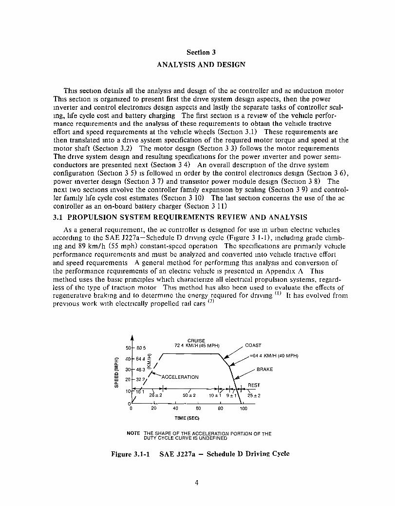
ThIS sectIOn detaIls all the analysIs and desIgn of the ac controller and ac mductIOn motor ThIs sectIOn IS orgaOlzed to present first the dnve system deSIgn aspects, then the power mverter and control electroOlcs deSIgn aspects and lastly the separate tasks of controller scalmg, lIfe cycle cost and battery charging The first sectIon IS a revIew of the vehIcle performance reqUIrements and the analYSIS of these reqUIrements to obtam the vehIcle tracttve effort and speed requIrements at the vehIcle wheels (SectIon 3.1) These reqUIrements are then translated mto a dnve system specIficatIOn of the reqUIred motor torque and speed at the motor shaft (SectIon 3.2) The motor deSIgn (SectIOn 3 3) follows the motor reqUIrements The dnve system deSIgn and resultmg specIficatIOns for the power mverter and power semIconductors are presented next (SectIon 3 4) An overall descnptIOn of the dnve system configuratIOn (SectIOn 3 5) IS followed m order by the control electroOlcs deSIgn (SectIOn 3 6), power mverter deSIgn (SectIOn 3 7) and transIstor power module deSIgn (SectIOn 3 8) The next two sectIons mvolve the controller famIly expanSIOn by scalIng (SectIOn 3 9) and controller famIly lIfe cycle cost estImates (SectIOn 3 10) The last sectIOn concerns the use of the ac controller as an on-board battery charger (SectIOn 3 11)
3.1 PROPULSION SYSTEM REQUIREMENTS REVIEW AND ANALYSIS
As a general reqUIrement, the ac controller IS deSIgned for use m urban electnc vehIcles accordmg to the SAE J227a-Schedule D dnvmg cycle (FIgure 3 I-I), mcludmg grade cltmbmg and 89 km/h (55 mph) constant-speed operatIOn The speCIficatIOns are pnmanly vehicle performance reqUIrements and must be analyzed and converted mto vehIcle tractIve effort and speed reqUIrements A general method for performmg thIS analYSIS and converSIOn of the performance reqUIrements of an electnc vehicle IS presented m AppendiX A ThiS method uses the baSIC prmclples whIch charactenze all electncal propulSIOn systems, regardless of the type of tractIOn motor ThiS method has also been used to evaluate the effects of regeneratIve brakmg and to determme the energy reqUIred for dnvmg (J) It has evolved from prevIOUS work With electrIcally propelled raIl cars (2)
£ Q.
~ c w w Q. en
CRUISE
50 805 72 4 KM/H (45 MPH) COAST
40 644 ~ "'644 KM/H (40 MPH)
483 g / 30 BRAKE
32;> r-ACCELERATION 20 I' 10
OL---~ ____ -L ____ -L ____ -L ____ ll-__
o 20 40 60 80 100
TIME (SEC)
NOTE THE SHAPE OF THE ACCELERATION PORTION OF THE DUTY CYCLE CURVE IS UNDEFINED
Figure 3.1-1 SAE J227a - Schedule D Driving Cycle
4

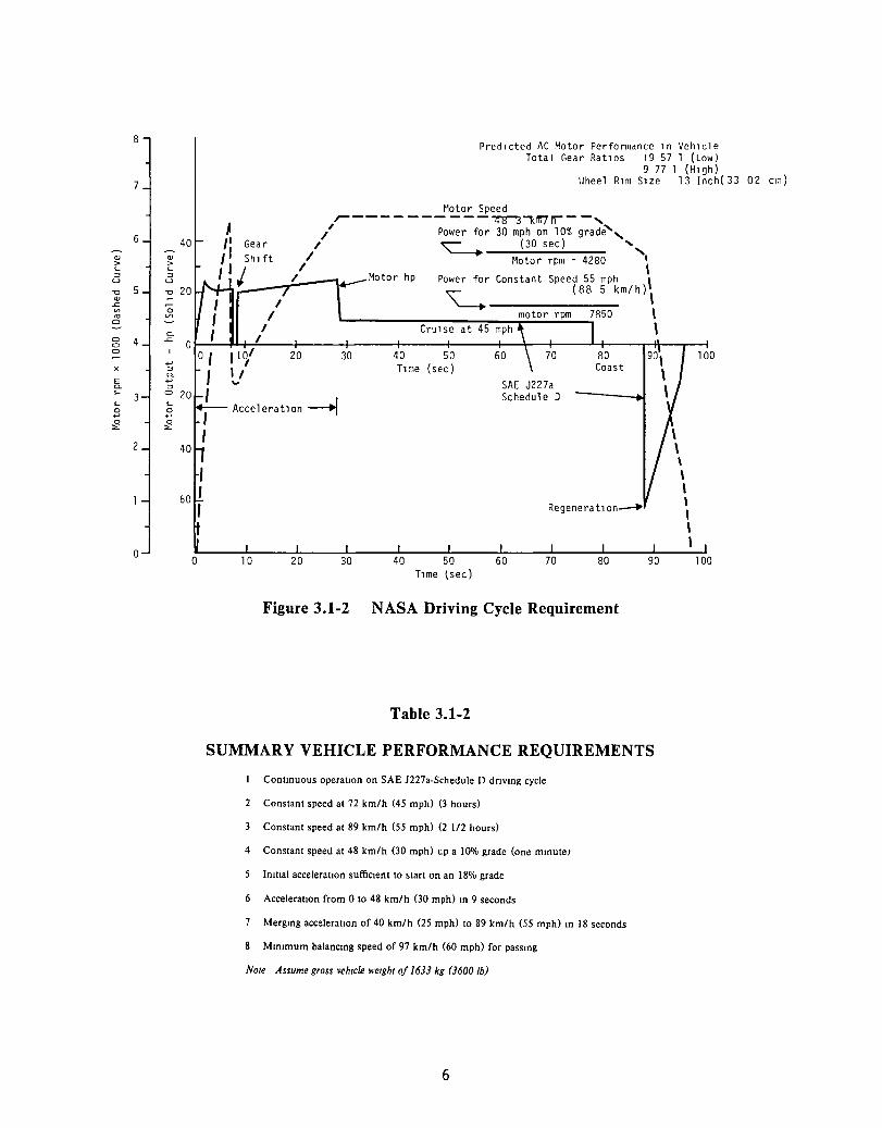
The NASA drIve system specificatIOns are presented In two parts The first IS entitled "Tentative Motor SpecIficatIons" Table 3 1-0 The second part of the specIficatIOn shows the power and speed requIrements for the ac motor to meet the SAE J227a - Schedule D drIVIng cycle (FIgure 3 1-2) ThIS cycle IS based on a vehIcle gross weIght of 1633 kg (3600 lb) and allows a two-speed transmISSIOn In addItIon, a practIcal electrIC vehIcle must satIsfy performance reqUIrements In excess of the J227a-D duty cycle In order to merge wIth traffic, start on a steep grade, pull out of a pothole, and pass AddItIonal specIficatIons have been added to the NASA specIficatIOns to account for these reqUIrements A summary of specIficatIOns IS shown In Table 3 1-2 The addItIonal specIficatIOns define the maXImum desIred vehIcle performance Several of these WIll occur only once or tWIce per battery charge The NASA specIficatIOns define the baSIC thermal ratIngs and performance These performance reqUIrements are analyzed In detatl In AppendIx A and the results of thIS analySIS are shown In FIgure 3 1-3 ThIS figure IS a vehIcle specIficatIOn of tractIve effort versus vehIcle speed at the vehIcle wheels
Table 3.1-1
TENTATIVE MOTOR SPECIFICATIONS
Frame S,ze NEMA 215TD (aluminum frame) or equIvalent
Type Three-phase, squlffel cage, induction
Horsepower 10 hp, nominal at 60 Hz, 1800 rpm
Voltage Rating 175/35 volts RMS dt 60 Hz (double Windings for series or parallel connected operatIOn)
Frequency 60 Hz, nominal
Speed Nominal 1800 rpm at 60 Hz
Speed Range 0 to 8000 rpm as per F,gure 3 1-2
Horsepower Range As per F,gure 3 1-2
InsulatIOn Class F
Duty Continuous driving cycle SAE 1227a, Schedule D, (2 hours)
Constant 72 km/h (45 mph) vehIcle speed (3 hours)
Constant 89 km/h (55 mph) vehIcle speed (2 112 hours)
Constant 48 km/h (30 mph), 10% grade (\ minute)
Cooling Forced aIr wIth external blower
Blower Rating 12 VDC, 120 W, 250 CFM thermostatIcally controlled
5
OJ > .. ::l
U
"0 OJ
.s:: Vl
'" Cl
C) C) C)
E c. .. .. o ..., o :.:
8
6
5
4
3
2
o
OJ > .. ::l
U
"0
o V>
40 Gear
Predlcted AC Motor Performance ln Vehlcle
t10tor Speed
Total Gear Ratlos 19 57 1 (Low) 9 77 1 (H1Dh)
Ilheel Rlm SlZe 13 Inch(33 02 em)
~----------~Km~--, /' Power for 30 mph on 10% grade',
/ ~ (30 sec) ..... I ~ " / Motor rpm = 4280 ,
/ Power for Constant Speed 55 mph , ' __ -r-- "'""" (88 5 km/h),
,/ ~ , c. I Crulse at 45 mph \
.s:: 0~~~~~/~--~------~----~------~----~--;---~--~~----1r~--~~ ..., ::l C. ..., ::l
C) 20 .. o ..., o :.:
o
II~' 1/ ..
20
Acce1eratlon ~
30 40 50 Tlme (sec)
Tlme (sec)
60 Coast
Regeneratlon~
Figure 3.1-2 NASA Driving Cycle Requirement
Table 3.1-2
SUMMARY VEHICLE PERFORMANCE REQUIREMENTS
Contlfiuous operatIOn on SAE 1227a-Schedule 0 dnvlfig cycle
Constant speed at 72 km/h (45 mph) (3 hours)
3 Constant speed at 89 km/h (55 mph) (2 112 hours)
4 Constant speed at 48 km/h (30 mph) up a 10% grade (one mlfiuteJ
Imtlal acceleratIOn sufficient to start on an 18% grade
6 AcceleratIOn from 0 to 48 km/h (30 mph) lfi 9 seconds
7 Merglfig acceleratIon of 40 km/h (25 mph) to 89 km/h (55 mph) lfi 18 seconds
8 MlfilmUm balanclfig speed of 97 km/h (60 mph) for passlfig
Note Assume gross vehicle weight of 1633 kg (3600 [b)
6
100
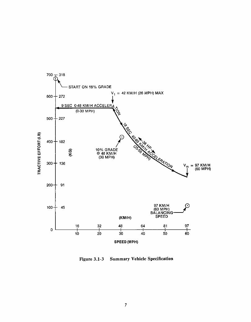
700 318
START ON 18% GRADE
272 V1 = 42 KM/H (26 MPH) MAX
• 600
9 SEC 0·48 KM/H ACCELERtl,>.
(0·30 MPH) "6 't-
500 227
iii' d. I- 400 182 a: 0 u. - 10% GRADE u. CJ w ~ @ 48 KM/H w -- (30 MPH) > j::: 300 136 0 Vm = 97 KM/H c:( a: (60 MPH) I-
200 91
100 45 97KM/H J (60 MPH)
BALANCING (KM/H) SPEED
16 32 48 64 81 97 0
10 20 30 40 50 60
SPEED(MPH)
Figure 3.1-3 Summary Vehicle Specification
7
3.2 MOTOR REQUIREMENTS REVIEW AND ANALYSIS
After a review of induction motor characteristics, this section takes the vehicle tractive effort and speed requirements at the vehicle wheels and translates them into the required motor torque and speed at the motor shaft.
3.2.1 Induction Motor Characteristics
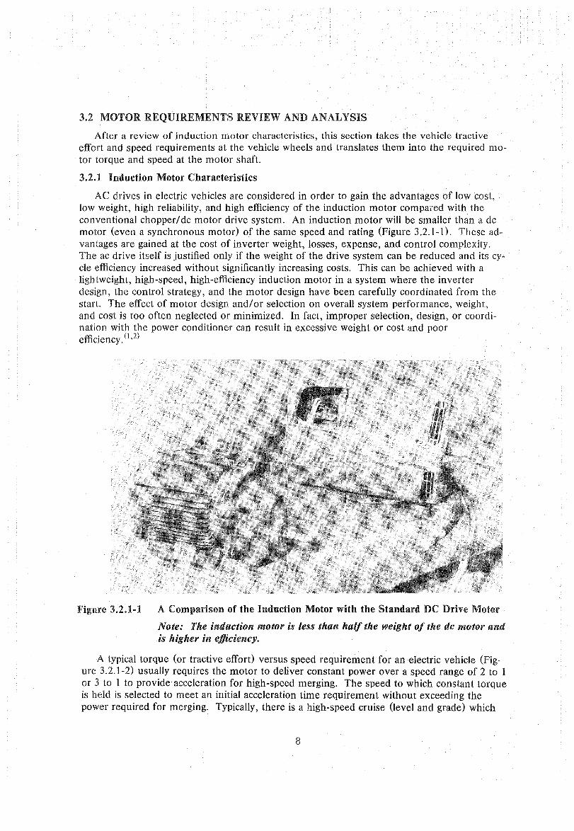
AC drives in electric vehicles are considered in order to gain the advantages of low cost, low weight, high reliability, and high efficiency of the induction motor compared with the conventional chopper/de motor drive system. An induction motor will be smaller than a dc motor (even a synchronous motor) of the same speed and rating (Figure 3.2.1-1). These advantages are gained at the cost of inverter weight, losses, expense, and control complexity. The ac drive itself is justified only if the weight of the drive system can be reduced and its cycle efficiency increased without significantly increasing costs. This can be achieved with a lightweight, high-speed, high-efficiency induction motor in a system where the inverter design, the control strategy, and the motor design have been carefully coordinated from the start. The effect of motor design and/or selection on overall system performance, weight, and cost is too often neglected or minimized. In fact, improper selection, design, or coordination with the power conditioner can result in excessive weight or cost and poor efficiency. (j,2)
Figure 3.2.1-1 A Comparison of the Induction Motor with the Standard DC Drive Motor
Note: The induction motor is less than half the weight of the dc motor and is higher in efficiency,
A typical torque (or tractive effort) versus speed requirement for an electric vehicle (Figure 3.2.1-2) usually requires the motor to deliver constant power over a speed range of 2 to 1 or 3 to 1 to provide acceleration for high-speed merging. The speed to which constant torque is held is selected to meet an initial acceleration time requirement without exceeding the power required for merging. Typically, there is a high-speed cruise (level and grade) which
8
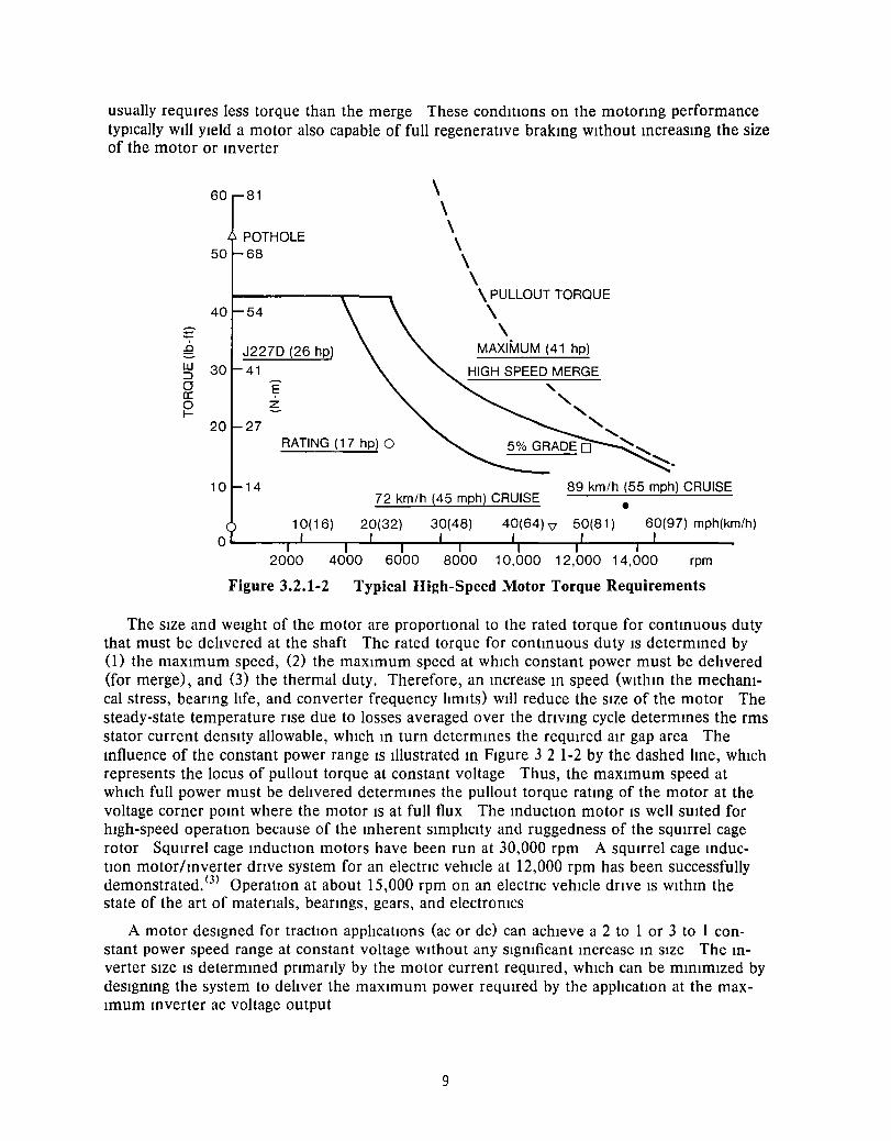
usually reqUIres less torque than the merge These conditions on the motorIng performance tYPically wIll YIeld a motor also capable of full regenerative brakIng wIthout IncreasIng the size of the motor or Inverter
60 81
POTHOLE 50 68
10 14
\ \ \ \ \ \
\ PULLOUT TORQUE
\ \
MAXIMUM (41 hpj
72 km/h (45 mph) CRUISE 89 km/h (55 mph) CRUISE
• 40(64) V'
O~----~----'-~--'---~-r----~----~~----'-~-------2000 4000 6000 8000 10,000 12,000 14,000 rpm
Figure 3.2.1-2 Typical High-Speed Motor Torque Requirements
The size and weight of the motor are proportIOnal to the rated torque for contInUOUS duty that must be delIvered at the shaft The rated torque for contInUOUS duty IS determIned by (1) the maximum speed, (2) the maximum speed at which constant power must be delIvered (for merge), and (3) the thermal duty. Therefore, an Increase In speed (withIn the mechamcal stress, bearIng lIfe, and converter frequency lImits) will reduce the size of the motor The steady-state temperature rIse due to losses averaged over the drIVIng cycle determInes the rms stator current density allowable, which In turn determInes the reqUIred air gap area The Influence of the constant power range IS Illustrated In Figure 3 2 1-2 by the dashed lIne, which represents the locus of pullout torque at constant voltage Thus, the maximum speed at which full power must be delIvered determInes the pullout torque ratIng of the motor at the voltage corner POInt where the motor IS at full flux The InductIOn motor IS well sUIted for high-speed operatIOn because of the Inherent simplIcity and ruggedness of the squIrrel cage rotor SquIrrel cage InductIOn motors have been run at 30,000 rpm A squIrrel cage InductIOn motorhnverter drIve system for an electrIc vehicle at 12,000 rpm has been successfully demonstratedYl OperatIOn at about 15,000 rpm on an electrIc vehicle drIve IS WithIn the state of the art of materIals, bearIngs, gears, and electronICS
A motor designed for tractIOn applIcatIOns (ac or dc) can achieve a 2 to 1 or 3 to 1 constant power speed range at constant voltage Without any slgmficant Increase In size The Inverter size IS determIned prImarIly by the motor current reqUIred, which can be mInimized by designIng the system to delIver the maximum power reqUired by the applIcation at the maxImum Inverter ac voltage output
9
The zero and low-speed torque may be Increased with a gearshIft, thus reducing the inverter current reqUired, but If the Inverter is sIzed by other consideratiOns (as It usually IS), there IS no advantage Even where there IS an advantage, studIes have shown that the weight-saving in the inverter and motor is largely negated by the added weIght of the gears (7)
Efficiency suffers because of the gear loss, especially at hIgh speeds, where lubncant pumping accounts for a sIgnificant portiOn of the loss
With proper deSIgn, the efficiency of the inductiOn motor will be hIgher than a dc motor whtle meeting the same performance reqUirements, as It must In order to compensate for the Inverter efficiency and motor harmonic losses A properly designed high-speed Induction motor will exhibit an almost constant, high efficiency over a wide speed range by keeping the magnetic, I2R, and mechanical losses In balance, as they can be With proper machine design, control strategy, and Inverter design To attain the hIghest effiCiency In the motor, It IS deSIrable to optimize the deSign at lower values of current and flux denSity, use lower resistance matenals for the rotor bars, and build With thinner lamInattons than normal SUitable matenals are commercially available for thiS type of design.
3.2.2 Motor Tractive Effort and Speed Requirement
The summary vehicle speCificatiOn In SectiOn 3.1 IS the vehicle tracllve effort and speed reqUirement at the vehicle wheels In order to establish the motor speCificatIons, It IS necessary to translate thiS reqUirement from the vehicle wheels to the motor shaft ThiS Involves including the rotary Inerlla effects of the dnve which must be dehvered by the dnve system, but do not appear at the wheels ThiS effect IS discussed In AppendiX A. USing those equations, the results show that the dnve system horsepower Increases to 41 hp and the maximum corner pOint speed reduces to 40 km/h (25 mph) The 10% gradablhty, inittal acceleration, and balancing speed specificatIOns are unchanged
The 40-89 km/h (25-55 mph) acceleratIOn requirement establIshes the dnve horsepower rating of 41 hp (Figure 3.22-1) ThiS sizes the power Inverter and motor The 10% gradabihty IS Inherently met If thiS acceleratIOn IS met (FIgure 3 2 2-D In fact, the actual performance would allow a 10% grade to be traversed at up to 58 km/h (36 mph), or a 13% grade could be clImbed at 48 km/h (30 mph).
The 0-48 km/h (0-30 mph) acceleratIOn reqUirement estabhshes the maximum corner pOint vehicle speed of 40 km/h (25 mph) The tractive effort at 40 km/h (25 mph) avaIlable from 41 hp IS 279 kg (615 lb) ThiS IS the constant tracttve effort aVailable from zero speed to the corner pOint The Inlllal acceleratton reqUires 309 kg (681 lb) of tracttve effort at zero speed If the motoring corner point IS reduced to 35 km/h (22 mph), the tractlve effort avallable from 41 hp IS 317 kg (698 lb). ThiS allows the InitIal acceleratIOn to be Inherently met and the 0-48 km/h (0-30 mph) acceleratiOn Will be shghtly better than 9 seconds This is accomplIshed at the expense of a Wider speed range for constant horsepower from the motor, but not sufficient to increase the motor size. Furthermore, thiS higher starting torque can be dehvered Without a higher current. The Inlttal acceleratIOn and 35 km/h (22 mph) corner pOint, VI> are shown In Figure 3.2.2-1.
If a constant horsepower speed range of 2 5 IS selected, then V2 = 86 km/h (55 mph) ThiS means the 97 km/h (60 mph) balanCing speed must be met With the dnve operatmg In RegIOn III, where the acceleration drops off as the reciprocal of speed squared ThiS pOint IS eastly met, as shown In Figure 3 2 2-1
The 72 and 86 km/h (45 and 55 mph) crUise requirements are also shown In Figure 3 22-1 They are found by using the methods discussed in AppendiX A.
10

The regeneratIve brakIng effort curves are shown In FIgure 3 2 2-1 The varIatIOn In ac current as a functIOn of battery charge, wIth the resultant varIation in brakIng effort, IS also shown The brakIng effort curves are a derIvatIve of the motorIng case and thus show the brakIng capabIlIty of the drIve relatIve to the deSIgned motorIng capabIlIty
800 363
700
..-600 I:C
:::::!. .... a: 500 227 0
u. a-u. w ~ w 400 182 > V2 = 89 KM/H (55 MPH) ~ 0 300 136 ~ a: 97 KM/H .... (60 MPH)
200 91 /BALANCING 72 KM/H (45 MPH) SPEED
100 45 (KM/H) CRUISE 7
£a9 KM~H (55 MPH) CRUISE 16 32 48 64 81 97
10 20 30 40 50 60
-100 -45 SPEED(MPH)
-200 -91
-300 -136 '" , ,
-400 -182 ~~~" ~~o ......
-500 -227 -<-~~~ ~~ .," ;;.'0 @ \';" '" ~s
~*"~;I' ~o~ -600 -272 <o~-, <o~~
~ / *-~ \l'~'i---700 -318 9 SEC 72-0 KM/H J227a-D
~/ 9:-~ @ ~ CYCLE <O:t-"<v 'l-X'
(45-0 MPH) 9:-~ ~'\ -800 -363 ::.<0
~~
-900 -409
Figure 3.2.2-1 Motor Tractive Effort and Speed Requirement
11
3.2.3 Motor Torque and Speed Requirement
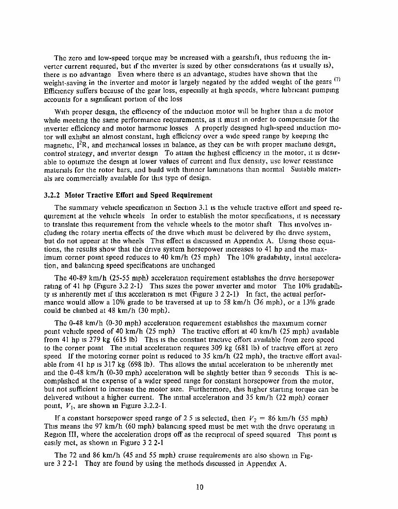
In order to establIsh the final motor speclficatlOn, It IS necessary to determme the motor speed as related to vehIcle speed The motor IS to be operated at about 15,000 rpm maxImum The mtegral gear box on the motor used to make the tractlOn motor compatible wIth standard automotlve axle geanng IS 2 923 to 1 Thus, 97 km/h (60 mph) whIch IS a gear box speed of 5000 rpm results m a motor speed of 14,615 rpm FIgure 323-1 shows the motor tractlve effort-speed reqUlrements of FIgure 3 2 2-1 converted to a motor torque-speed curve, assummg a gear box efficIency of 95%
50 68
45 61
40 54 START ON
18% GRADE
35 47 t=' LL ID 30 41 :::!. ::i w
25 ~ 34 ~ 0 II: 0 20 27 I-
0 15 20 17 HP
J227a D RATING
10 14 97 KM/H (60 MPH) BALANCING SPEED
0 0 5 7 0
72 KM/H (45 MPH) CRUISE 89 KM/H (55 MPH) CRUISE
0 2 3 4 5 6 7 8 9 10 11 12 13 14 15
-5 -7 SPEED (RPM - 1000)
-10 -14
-15 -20 , ,," , , -20 -27
, " ,,/
-2 -34 X. ,," \>-'f.: .. ~ .. "','0 ......
-30 -41 ~'O~".., :tS ,. ~~,," ~\>-'f..x.
-35 -47 ,," ",\'0 , 'l..~
J227a D CYCLE BRAKE ' ~ -40 -54
~,?-i-
-45 -61 MAX BRAKE
-50 -68
Figure 3.2.3-1 Motor Torque and Speed Requirement
12
The peak power and torque reqUIrements to meet the J227a-Schedule D dnvmg cycle are somewhat less severe than the maximum peak values, but must be met with a reduced battery voltage due to dnvmg with a nearly discharged battery When operatmg on the J227aSchedule D duty cycle, the vehicle must operate for a penod of time longer than the motor thermal time constant, thus, this operatIOn will define the contmuous thermal ratmg of the motor The maximum performance requIrements are for short-time overloads of the traction motor and thus Will not slgmficantly affect the steady state ratmg However, the motor must have enough peak torque capability to produce the desIred performance The maximum performance IS With a fully charged battery Full regenerative brakmg IS available and desIred for the J227-a - Schedule D duty cycle Some of the conditions will occur only once or tWice per battery charge
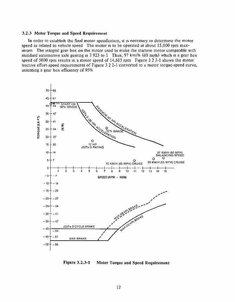
3.2.4 Equivalent Motor Rating
In order to calculate the ac motor current for thermal ratmg purposes, a schedule of voltage as a functIOn of speed IS reqUIred This schedule and the resultmg ac motor currents are descnbed m detaIl m SectIOn 3 4 Consldermg the J227a-D cycle, usmg this voltage and the requIred torque, the ac motor current can be calculated for the reqUIred duty cycle The results are shown m Figure 3 2 4-1 The rms value of the ac motor current over the total time of 122 seconds Yields an eqUIvalent power ratmg of 17 hp at 35 km/h (22 mph) The motor was bUIlt usmg a standard 180 frame, which IS smaller than the NASA-specified 215 frame The motor weight IS about 45 kg (100 lb)
400 r-
"in
MAX BATTERY (140 VDC) -----
FULL BATTERY (100 VDC)---
LOW BATTERY (75VDC) --------:;;
~ 300r\---------: r----' -
a: =» (J
a: o Io :E
200r--
100r--
o
i i . I i
- - - - ----------- ------ i i
I I i i 10 20 30 40 50 60 70 80 90 100 110 120 130
TIME (SEC)
Figure 3.2.4-1 AC Motor Current for J227a-Schedule D Duty Cycle
13

3.3 MOTOR DESIGN
The GE-optimizcd motor is designed to operate as a vehicle traction motor with a pulse width modulated inverter as a power source. The motor is designed to maximize drive train efficiency, minimize inverter size, eliminate excess gearing, and to be producible by automated manufacturing processes. To further this aim, a standard 180 motor frame and a conventional integral gear box are used to make the traction motor easily usable with standard automotive axle gearing. This section describes the motor design.
3.3.1 Motor Description
The design of a motor for use with an inverter power supply must take into account the presence of time harmonics in the voltage and current. (4,5) In some cases, it is possible to design the motor and inverter so that the harmonics will produce useful torque resulting in increased efficiency and lower weight. (6) Usually, however, the thermal capability of the motor must be increased to accommodate harmonic losses. Double-cage rotors are not needed; coffin-shaped bars are preferred for an inverter-powered motor. Other factors entering into the motor design include: end winding vibration due to harmonics, forces developed as a result of inverter shoot-through, torque pulsations, and voltage "pileup" due to high dV / dt.
The motor is shown in a disassembled view in Figure 3.3.1-1. It is a four-pole design and has a maximum frequency given by:
where
f = np Hz 60
n =the speed in rpm (14,615)
p = the number of pole pairs (2)
Therefore, f = 487 Hz.
Figure 3.3.1-1 The Optimized Induction Motor Disassembled
14

The double-cage rotors often supplied on standard InductIOn motors In this size range are not required SInce startIng will not be done on a fixed frequency lIne Indeed, the exotic and multitudInous vanetIes of double cages, saturable shunts, and rotor bar shapes that are supplied In the standard Inventones will lead to Increased harmOnIC losses In most cases The GE optimized motor uses coffin-shaped rotor bars, that IS, the teeth have parallel sides and the bars are wider at the top than at the bottom This achieves two objectives for Increased efficiency 1) the maximum conductor area In the rotor to reduce rotor loss, and 2) the rotor bar IS as Wide as pOSSible In the regIOn where harmOnIC currents are concentrated to reduce harmOnIC losses In addition, SInce startIng torque In the conventIOnal sense for a standard motor IS not reqUIred With the Inverter dnve, the rotor bars are high-conductivity copper
In cOmbInatIOn With the large conductor area, a very low rotor resistance for the fundamentaliS achieved In the GE optimized motor. The torque speed charactenstIc IS, as a result, very steep and operatIng slips are very low, hence, rotor slip loss IS reduced to a minImum The motor appears to operate almost as a synchronous motor
The stator copper IS also maximized to reduce losses A speCial lamInatIOn With large slots IS used A commercial motor deSign seeks to mInimize the amount of copper In comparIson to Iron In order to reduce materIal costs The amount of copper In the slot IS maximized by USIng a tightly packed WIndIng, thInly coated InsulatIOn, and a SIngle, rather than a dual, WIndIng Class H materIals are used for the turn, ground, and phase InsulatIOn In the stator The overall temperature ratIng IS Class F due to the ImpregnatIOn materIal
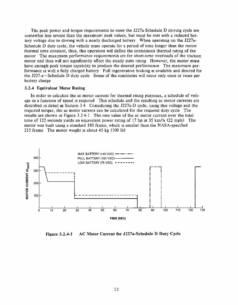
A cruCial and difficult Item IS the materIal and IntegrIty of the lamInatIOns In a commerCial offerIng, the stator lamInatIOn materIal IS most often a low carbon steel of 0 064 cm (0 025-Inch) thickness ThiS IS adequate for most applicatIOns where effiCIency IS not paramount In motors where high effiCiency IS demanded or where a serIOUS steady-state overheatIng problem has been encountered, a 2 6% SIlicon steel of 0 048 cm (0019 Inch) Will often be used Sometimes lamInatIOns as thIn as 0036 cm (0014 Inch) (at a premIUm prIce) may be used The GE optimized motor utilizes a high-quality 3 25% SIlicon non-orIented steel 0018 cm (0007-Inch) thick The high SIlicon content reduces hysteresIs loss and Increases the resistivity which, In conjunction With the small thickness, reduces eddy current loss ReductIOn of eddy current losses are relatively more Important In a varIable speed drIve SInce they vary as frequency squared, whereas, hysteresIs loss vanes directly WIth frequency High-frequency Inverter harmOnICs also must be conSidered Hence, It IS deSIrable to use the thInnest lamInatIOn consistent With low hysteresIs loss and economics It IS pOSSible to further reduce the core loss In the GE optimized motor by USIng a more expensive nIckelbased alloy or by redUCIng flux denSity (and IncreaSIng the weight) The flux denSity selected IS less than that used In commerCial offerIngs but still higher than the Ideal In order to stay WIthIn the 180 frame size At the selected flux density, the effiCiency IS, however, satisfactOrIly high over the speed range The stator and rotor punchIngs of the G E optimIzed motor are shown In Figure 332-2 They were made by an etchIng process
SInce the lamInatIOns are very thIn, conventIOnal varnIsh coatIngs would be unacceptably thiCk, leadIng to a very low stackIng factor, hence, a very thIn (less than 10-4 cm) glassy coat was utilized An added benefit IS a much higher temperature and dielectrIC capability ThiS coatIng had to be applied to the bulk materIal whIch In turn reqUIred extensive development of a speCial etchIng process Normal commercial machIne practice IS to utilize the natural OXide coat
15
Figure 3.3.1-2 The Stator and Rotor Punchings of the GE Optimized Motor
Note: The coffin shape of the rotor bar area.
In conventional machines, the rotor laminations are often made very thick and from the cheapest available materials since the bulk of the rotor iron is excited at very low (slip) frequency. However, a significant source of loss in the rotor is due to slot and mmf fluctuations at the rotor surface, which may be of relatively high frequency. Inverter harmonics will also cause high frequencies in the rotor. In order to reduce these losses, the rotor is made from the same material as the stator. This did not materially increase cost since the etching process developed allowed the rotor to be fabricated at the same time as the stator in the stator bore region, out of material that would be scrap in the normal production process.
The end windings of an inverter driven motor should be braced better than a conventional motor to withstand high-frequency excitations due to inverter harmonics. More importantly, the motor will be subjected to inverter "shoot-throughs" and "crowbars," which can result in extremely high forces in the end windings, as well as in the shaft.
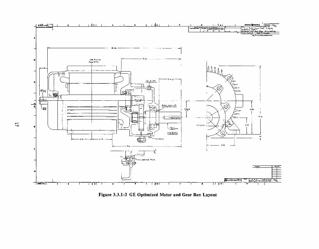
To reduce fabrication cost and time, the GE optimized motor utilizes a standard aluminum 180 frame and end bell. A special end bell with integral gear box is used to reduce the speed from 14,615 rpm to 5000 rpm to interface the standard applications. The layout of the motor and gearbox is shown to scale on drawing ESD-I96 (Figure 3.3.1-3). The principal dimensions of the motor outline and interface are also shown. The drive end bearing is lubricated from the gear box. However, as shown on the drawing, an end bell with a grease lubricated bearing may be used to provide a 15,000 rpm interface.
16
...... .......
...
•
E
p
H
£$6-, .. ,:--
".
:=.-:..,
1e"" F ..... _ .. I~-:- .... ""
,& ... ------ - ---
7
---------1
I'O.'----! I
~·'TI /,';" II (I * .. 11-5" ..
.s ..... , .,.,stJ, ....
~
-- ", ----------
~~\r-==~
H-",,,' X _ Yi*0
r------.,s
Figure 3.3.1-3 GE Optimized Motor and Gear Box Layout
II11IAL81umiC I=~E!- .,,<;Li'c:T>.l .. ,~·J!..t:.a ... Rcl.: ~ ~, f\
""·' ....... sD".'.,.~1

3.3.2 Advantages of the GE Optimized Motor
Advantages accrue m all areas of the electnc vehIcle and Its dnve system If a motor and power condItIoner are desIgned together both for a best match to each other and to the applIcatIon at hand Other consIderatIOns may mfluence the degree of matchmg and optImIzatIOn that can be done, such as the needs of automated mass productIOn or mterchangeabIlIty of components among vehIcles of differmg SIze and/or mISSIOn Such compromIses WIll always result m reduced performance and mcreased costs for moderate productIOn quantItIes, although economieS of scale and standardIzatIon may reduce costs m very large productIOn quantIties
In thIS case, It IS desIrable to optImIze the system as far as possible. There are a number of advantages to usmg the GE optimIzed motor rather than a standard Ime startmg mductIOn motor
• The mverter kVA ratmg IS reduced by 15% to 30%, whIch results in as much as a 2-to-l dIfference m mverter SIze and cost ThIS IS due to the motor bemg desIgned for an mverter power source, with an optImIzed motor-mverter voltage and current schedule, and reduced motor harmonIc loss, I2R loss and magnetIc loss
• The gearshift and clutch mechanIsm with ItS associated relIabilIty and loss problems are elImmated
• The motor SIze IS small and utIlIzes a 180 frame
• The motor efficIency IS maXImIzed.
• Inverter efficIency WIll be hIgher due to the restnctIOn of the PWM mode to about onethIrd of the speed range
18

3.4 SYSTEM DESIGN AND CONTROLLER REQUIREMENTS
The system desIgn dIrectly relates the motor charactenstics to the Inverter desIgn. ThIS sectIOn shows the motor performance and descnbes the effect of the motor on the Inverter desIgn The results are a set of Inverter specificatIOns, IncludIng system voltage, and a set of power semIconductor specificatIOns The use of a multIple speed transmISSIOn IS not requIred
The basIc factors to be consIdered In the system desIgn are
1. Battery system voltage
2 Motonng corner POInt speed
3 Use of a ShIftIng transmIssIOn
4 Motor pull-out slIp
5 Motor voltage and current schedules
3.4.1 System Voltage
The battery system voltage chOice IS based on vehIcle arguments and transIstor voltage capabIlIty From prevIOUS work on a dc dnve system of basIcally the same vehIcular performance reqUIrements, a 108 volt battery voltage was chosen (8) The GE power DarlIngton transIstors (CRD-3 chIp) used In that program were capable of sWItchIng about 220 volts (the breakdown voltage was 300 volts) Power zener dIodes were needed to clIp the overshoot voltage to that level The Improved verSIOn (ZJ504) IS capable of sWItchIng about 300 volts WIth the expected overshoot voltages dunng transIstor sWItchIng, a transIstor voltage reqUIrement of tWIce the maXImum battery voltage IS mandatory The use of a 108 volt battery (18, 6-volt umts) wIll gIve a maXImum dc voltage of about 140 volts dunng regeneratIve brakIng Thus, the 108 volt nomInal battery IS about the maXImum system voltage that can be used due to the expected voltage tranSIents of up to about 300 volts on the transIstors
3.4.2 Motoring Corner Point Speed
The motonng corner POInt IS chosen so that a ShIftIng transmIssIon IS unnecessary In order to achIeve thIS obJectIve, the startIng torque must not reqUIre a hIgher motor current than the full-power, hIgh-speed motonng current A corner POInt (maXImum speed at whIch constant torque IS possIble) of 35 km/h (22 mph) at maXImum battery charge wIll satIsfy thIS reqUIrement The motor torque capabIlIty must also be suffiCIent to allow two other condItIons to be met The first IS that constant maXImum power be avaIlable to 89 km/h (55 mph) at full battery voltage The second IS that the 1227a-D power be carned to 72 km/h (45 mph) at low battery voltage
3.4.3 Motor Voltage and Current Schedules
The motor voltage and current schedules, along WIth the corner POInt speed, optImIze the SIze of the Inverter and motor and ehmInate the need for a ShIftIng transmIssIOn The schedules are shown In FIgure 3.4.3-1 for a nommal dc battery system voltage of 108 volts The motor voltage IS pulse-wIdth-modulated to mcrease hnearly up to the maXImum square wave motor voltage, where It becomes constant over the remaInder of the speed range The motor voltage schedule vanatIOn WIth battery voltage IS apparent In FIgure 343-1, wIth the maXImum square wave motor voltage IncreaSIng from 59 to 109 volts rms as the battery ranges from 75 to 140 volts dc The voltages shown are hne-to-hne fundamental rms voltage
19

MOTOR CURRENT
(ARMs!
600
500
400
300
200
100
LINE TO LINE MOTOR
VOLTAGE (VRMs!
120
100
80
I
I
I I
I
VLL @ MAX BATTERY-BRAKING (140 VDC) ,------------------
/ VLL @ LOW BATTERY-BRAKING (115 VDC) 1-------------------/-______ ::.L!:.:~U_=~B.:":::.:~=_~<:.T~~~NG (100 VDC)
MAX PERFORMANCE CURRENT @ FULL OR MAX BATTERY - MOTORING OR BRAKING
60
40
I 20 I
I I
I I
I I
I I
I
16
10
I
I I
I
I I VLL @ LOW BATTERY-MOTORING (75 VDC) ------------ ---------
J227a D CURRENT@ LOW BATTERY-MOTORING
J227a D CURRENT@ FULL BATTERY-MOTORING
o 72 KM/H(45 MPH) CRUISE @ LOW BATTERY
o 72 KM/H(45 MPH) CRUISE @ FULL BATTERY (KM/H)
32 48 64 81 97
20 30 40 50 60
SPEED (MPH)
Figure 3.4.3-1 Motor Voltage and Current Schedules
The fundamental rms ac motor current can be calculated for motonng operatIOn from the following equation
lac = 078 EB.J3 TIM TlG PF
where,
Po =dnve system output power III watts
EB =battery voltage III volts
TIM =motor efficiency (090)
TlG =gear efficiency (095)
PF =motor power factor (080)
This equatIOn assumes some values for efficiency and power factor, and IS valId for a motor square wave voltage waveform The current schedules are also shown III Figure 3 4 3-1 In the motonng maximum performance case, the motor current IS 330 amps rms, based on the reqUIred 41 hp at full battery (IOO VDC) This motor current is, then, the current avaIlable for the regenerative braking maximum performance case. For the motonng portion of the J227a-D duty cycle reqUIrement, the motor current starts at 330 amps rms and drops off to 280 and 210 amps rms for low battery (75 VDC) and full battery (100 VDC) respectively, based on the reqUIred 26 hp.
20
These motor voltage and current schedules result In the motor performance as requued In FIgures 3 2 2-1 and 3 2 3-1 In the motonng maXImum performance case at full battery, the motor current IS held constant whIle the motor voltage Increases lInearly up to the motonng corner POInt speed of 35 Km/h (22 mph) In thIS case, the corner POInt occurs when the motor voltage reaches the maXImum square wave value Thus, the motor IS operated at constant volts/hertz up to the motonng corner POInt speed and the motor torque IS constant Thereafter, the motor current and voltage are both constant and the motor operates at a constant horsepower hmlt In the motorIng portlOn of the J227a-D duty cycle case, the motor current IS held constant whIle the motor voltage Increases lInearly up to the motonng corner POInt speed of 23 Km/h (14 mph) This agaIn results In a constant motor torque output In thIS case, the motonng corner POInt speed IS set by the reduced torque reqUIrement, rather than the motor reachIng maXImum square wave value Thereafter, a constant horsepower IS desired, so the motor current IS allowed to drop off as the motor voltage contInues to nse hnearly up to the square wave value at 26 Km/h (165 mph) or 35 Km/h (22 mph), dependIng on the battery voltage After thIS speed, the motor voltage and current are both constant, as before In regenerative brakIng maximum performance, the corner POInt moves up to 50 Km/h (31 mph) and the current IS held constant, SimIlar to the motorIng performance
The Inverter IS not reqUIred to operate In the pulse-wIdth modulatIOn mode over the hIghspeed portIOn of the speed range, thus considerably redUCIng the Inverter losses and IncreasIng system effiCiency The proper chOIce of the motor voltage schedule affects both Inverter SIze and motor SIze In addItion, the system effiCIency IS Increased by a SUItable chOIce of motor voltage schedule
3.4.4 Motor Performance
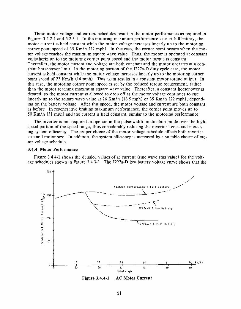
Figure 3 4 4-1 shows the detaIled values of ac current (sIne wave rms value) for the voltage schedules shown In Figure 343-1 The J227a-D low battery voltage curve shows that the
400
,/ MaXlmum Performance @ Full Battery ~/
----- \ -----V> 300 ::0::
'" "" -------------- '\ ... <=
J227a-O @ Low Battery '" .. .. =>
u .. 20G 0
'tJ227a-O @ Full Battery
... 0
::0::
'; ... <=
'" E
'" "0 <= 100 => ....
16 32 48 64 81 97 (km/h) 0
10 20 30 40 50 60 Speed - mph
Figure 3.4.4-1 AC Motor Current
21
current requIred IS a lower value than the maximum performance curve current Thus, the dnve will actually be able to dehver the reqUIred J227a-D performance wIth a battery which IS more than 80% discharged smce stIll more current can be delIvered The current mcrease at high speed on the maximum performance curve IS due to operatIOn very near to pUll-out motor slIp At lower speeds, there will be a signIficant percentage of harmonIc current which will add to the fundamental component of current shown m Figure 344-1 At higher speeds, the harmonIc currents wIll be reduced due to the higher frequency, thus, there will be more useable fundamental frequency mverter current capacity avaIlable to mamtam output power
Note that the maximum mverter current reqUIrement occurs at speeds over 40 km/h (25 mph) At these speeds, vehicle performance IS lImited by the peak power capacity of the mverter Use of a shlftmg transmiSSIOn will not reduce the reqUIrement for the high-speed current At low speeds, as long as the motor can delIver the reqUIred startmg torque Without a higher current, a shlftmg transmiSSIOn IS not reqUIred or desIrable
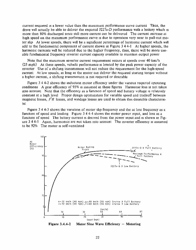
Figure 3 4 4-2 shows the mductlOn motor effiCiency under the vanous requIred operatmg conditIons A gear effiCiency of 95% IS assumed m these figures HarmonIc loss IS not taken mto account Note that the effiCiency as a functIOn of speed and battery voltage IS relatIvely constant at a high level Proper design optimizatIOn for vanable speed and tradeoff between magnetic losses, /2 R losses, and wmdage losses are used to obtam thiS desirable charactenstIc
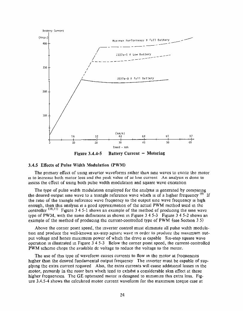
Figure 3 4 4-3 shows the vanatIOn of motor slIp frequency and the ac lIne frequency as a functIOn of speed and loadmg Figure 3 4 4-4 shows the motor power mput, and loss as a functIOn of speed The battery current IS denved from the power mput and IS shown m Figure 3 44-5 Agam, harmOnICS are not taken mto account The mverter effiCiency IS assumed to be 92% The motor IS self-ventilated
100
AC Motor Efflclency (%)
90
80
70
1 0
o~ 72 km/h X~ 72 km/h
16 I
10
Figure 3.4.4-2
L:. Motor Ratlng J227a-O @ Full Battery
pOln~t ___________ ~.i.. +
__ ---- Maxlmum Performance @
--,.......-- - _ --- _ / Full Battery ,""'-- - -- -- --~ ~ ..... ,--- --
J227a-O @ Low Battery
(45 mph) ,6-89 km/h (55 mph) Crulse @ Full Battery (45 mph),"'~89 km/h (55 mph) Crulse @ Low Battery
(km/h) 32 48 64 81
I I I I 20 30 40 50
Speed (mph)
Motor Sine Wave Efficiency - Motoring
22

50 25
L1ne Frequency ( hz)
S 11 P Frequency (Hz)
400 20
300 IS
L1ne Frequency Max1mum Performance @ Full Battery
MaX1mum Performance--~~~~---S11P Frequency
/ /
/ / /
I
/ /
.£L-~_-7/.!.-__ J227a-O@LowBattery //' 7 S11P Frequency
200 10 /' /
",/ /
100
Mo tor Power Input
(kW) 40
30
20
10
0
o
0
/ '" " ;/ / __ --___ 7'- - / / /-.,. Battery
32
(km/h)
48 64
W W E ~ Speed - ~h
81
50
Figure 3.4.4-3 Line and Slip Frequencies Motoring
Mo tor Loss (kWl 4
3
--- Motor Power Input
----- Motor Loss
MaX1mum Performance @ Full
" "
" " "
/
" / -" / I', ;'/. '.... - -- / " ,/ ........ _-- / / " / /
/ \"/ ,,//
/ \ ,,/
/
/ \ ..... '" I' _---@LowBattery-. -I "<- _
/ ~,-.....,." <" @ Full Battery...)'
21/ " l wlth harmon1cs j '~ (est1mated)
, --....... _-------- ------
16 32 (km/ h)
4 64 8
10 20 30 40 50 Speed - mph
/
/ /
/
J227a-0
Figure 3.4.4-4 Motor Power Input and Loss Motoring
23
97
60
9
60
Battery Current
(Amps)
400
300
200
100
a
I
16
10
I I
/ /
/
MaXlmum Performance @ Full Battery ----------/----- ------
J227a-D @ Low Battery __ -
/ ---------------------
J227a-D @ Full Battery
32
20
(km/h) 4B
30
Speed - mph
64
40
81
50
97
60
Figure 3.4.4-5 Battery Current - Motoring
3.4.5 Effects of Pulse Width Modulation (PWM)
The pnmary effect of usmg mverter waveforms rather than sme waves to excIte the motor IS to increase both motor loss and the peak value of ac Ime current An analysIs IS done to assess the effect of usmg both pulse WIdth modulatIOn and square wave excItatIOn
The type of pulse WIdth modulatIOn employed for the analysIs IS generated by companng the deSIred output sme wave to a trIangle reference wave whIch IS of a hIgher frequency (9) If the ratIo of the tnangle reference wave frequency to the output sme wave frequency IS hIgh enough, then thIs analYSIS IS a good approxImatIOn of the actual PWM method used m the controller (10,11) FIgure 345-1 shows an example of the method of producmg the sme wave type of PWM, WIth the same definItIons as shown m FIgure 345-3 FIgure 3 4 5-2 shows an example of the method of producmg the current-controlled type of PWM (see SectIon 3 5)
Above the corner pomt speed, the mverter control must elImmate all pulse WIdth modulatIon and produce the well-known six-step square wave m order to produce the maXImum output voltage and hence maXImum power of whIch the dnve IS capable SIx-step square wave operatIOn IS Illustrated m FIgure 3 4 5-3 Below the corner pomt speed, the current-controlled PWM scheme chops the avaIlable dc voltage to reduce the voltage to the motor.
The use of thIS type of waveform causes currents to flow m the motor at frequencIes hIgher than the deSIred fundamental output frequency The mverter must be capable of supplymg the extra current reqUIred Also, the extra currents wIll cause addItIonal losses m the motor, pnmanly in the rotor bars WhICh tend to exhIbIt a considerable skm effect at these higher frequencIes. The GE optImIzed motor IS deSIgned to mmImIze thIS extra loss. FIgure 3.4.5-4 shows the calculated motor current waveform for the maXImum torque case at
24

80% of the corner POInt speed (136 Hz) and full battery voltage The fundamental torque producIng component of ac current IS 328 amps rms and the peak current that the Inverter must commutate IS 592 amps The choppIng frequency IS twelve tImes the fundamental frequency of 136 Hz FIgure 3 4 5-5 shows a sample prInt out from the harmOnIC analysIs program shOWIng some of the detaIls avaIlable Note at the bottom of the pnnt-out the two effiCIency figures and the harmOnIC loss The effiCIency loss IS 1 4% and the harmOnIC loss IS 044 kW Figure 3 4 5-6 shows the effect of IncreaSIng the choppIng frequency to eighteen times the fundamental The current begInS to more closely approximate a SIne wave and the harmOnIC losses decrease to 034 kW ThIS demonstrates the convergence of the current waveshape of the SIne wave PWM analYSIS at high chOPPIng ratIOs With the current waveshape of the current-controlled PWM technIque The motor current for the six-step square wave operatIOn of the Inverter at the corner POInt speed of 180 Hz IS shown In FIgure 345-7 The results of thIS analYSIS Indicate that chOOSIng a maximum chOPPIng frequency of 3000 Hz WIll keep the peak currents to less than 600 amps and reduce the harmOnIC effiCiency loss to under 1% Motor currents and voltages under actual operatIOn are shown In SectIOns 4 6 and 47
Figure 3.4.5-1 Generation of Sine Wave PWM
25

/
REFERENCE WAVEFORM
ACTUAL CURRENT
Figure 3.4.5-2 Generation of Current-Controlled PWM
o
D [,
DD D
Figure 3.4.5-3 Generation of Six Step Square Wave
26

+700-- ----- - -- - -- - - -
/
o ~- --- - -:;. - - ---- -- -~--- - -- --....... ----,
-700---------- -
Figure 3.4.5-4 AC Motor Current for 12X PWM
COMfilTE-Itf'lRMUN 1 CS
COMPUTE LOSSES + 10ROUES VIIC= 108
PHASES= 3
I1E[f FAfi fiOTO~ [FFELT
COkE LOSS INCLUDED
HO 18
BAr~ WIDTHS B8= .099
SO .0123::;98
B9~- .187
MOTOfi FAfiAMETEfiS fi1 R~
2.96000E-03 1.44000E-03
K 11 AMPS
464
FILE FOfi CUfifiENT DK:IMHA7
I "115 TOT~ 34~ I Rt1S HAR= 96 I f\MS FUti" 3"0-_u
V ~MS FUN:- 36
HAI,I1 AMfL
.4768 50 -5.60000E-03 HAr,MONIC LOSS= .44 1\14
FO 180
LT .0~07::;
FF
.84::;1
HARMS TOTALS
SENSE
-1
VO 45
III .43
I~~*fi
WATTS 9::;7
81 1038
INF Ul 1\14
30.3 30.::;4
SlAT
146 .03
r,3 2.'16000(-06
I-~*fi !'-OT WATTS 363
157 519
TOT LOSS 1\14
1.05 ~.:!9
Figure 3.4.5-5 Harmonic Results for 12X PWM
27
r: 136.
4
LOfiF WHTl 5:?7
:!O5 733
FFFI
.93'1
.92~

+ 700 .- .... ------------------ --
i /
-/
a /
~ -700 ----
Figure 3.4.5-6
+700 - - ---- ---- - ----
" /
:
AC Motor Current for 18X PWM
a .- ------ ---------- ----- -----,--- -- ----- -----
-"'-i,_. '-..
',v
-700 -- -.-------- -- - ---- ----------- --- --- - -- -- -- ---- --- - ---- ------ - ---- - ---------- --,
Figure 3.4.5-7 AC Motor Current for Square Wave
28

3.4.6 Motor Leakage Reactance and Harmonics
The InductIOn motor eqUlvalent CIrCUlt for the fundamental frequency IS shown In FIgure 34.6-1a. ConslderIng the harmonIcs, the rotor reslstance at the fundamental frequency appears as a short circUlt, thus only the leakage Inductance and motor resIstance are In the circUlt to IImlt the harmonIc currents (FIgure 3.4 6-1b) The values for the motor parameters of FIgure 3.4.6-1 are
Rs =000298 n RR =000145 n LM =000024 H
Ls =000001269 H
LR =000001015 H
P =4 poles
Rs Ls Lr Rr
V SIN wT Rr C ;s)
S = SLIP FREQUENCY w = STATOR FREQUENCY
w
(A) FUNDAMENTAL FREQUENCY EQUIVALENT CIRCUIT
Rs Ls Lr Rr
wH = HARMONIC FREQUENCY
(8) HARMONIC FREQUENCY EQUIVALENT CIRCUIT
Figure 3.4.6-1 Induction Motor Equivalent Circuits
29

The harmonIc losses can be calculated from the folloWIng equatIOns
V" _ Vh Ih = -,-----------(Rs+RR) + }wlt (Ls+LR) - }W" (Ls+LR)
where,
V" = harmonIc voltage
I" = harmollic current
wit = harmonIc frequency
The GE optimIzed motor IS desIgned to supply constant torque wIth constant flux up to the corner POInt and constant power to near maxImum speed wIth constant voltage applIed The leakage Inductance IS maxImIzed consIstent WIth the constant power reqUIrements (I)
MaXImIZIng the leakage Inductance mInImIzes the harmOnIC currents, but lImIts the pUll-out torque and thus the maxImum speed for constant power output at constant applIed voltage The leakage Inductance IS Important also In the operatIOn of the current-controlled PWM techlllque (I J) The maxImum leakage Inductance IS gIven by (2)
o 0410E# LT ~
where,
LT =leakage Inductance In henrIes
EB =battery voltage In volts
Po =drIve system output power In watts
V2 =speed at end of constant power regIOn In mph
12 =motor frequency at V2 In hertz
3.4.7 Controller and Power Module Requirements
The controller reqUIrements are extracted from thIS system deSIgn and are shown In Table 3 4 7-1 SInce the power semIconductors In the Inverter have a very short (1 second) thermal time constant, they are SIzed for the peak Inverter currents The thermal ratIng of the Inverter must be larger than the J227a-D duty cycle ratIng, so It can handle the peak loads Its thermal tIme constant (several mInutes) IS faster than the motor time constant, and of the order of the duratIOn of the peak loads Therefore, the Inverter IS thermally deSIgned to operate nearly contInuously at the peak loadmg reqUIrements
30
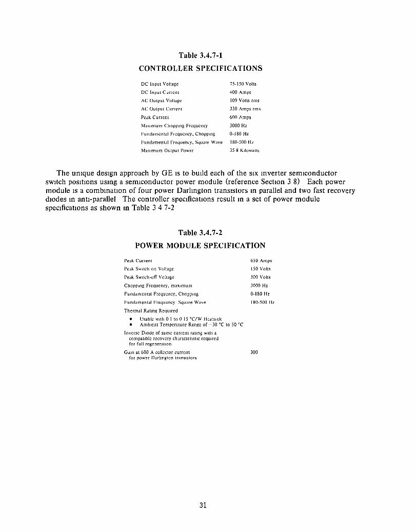
Table 3.4.7-1
CONTROLLER SPECIFICATIONS
DC Input Voltage 75-150 Volts
DC Input Current 400 Amps
AC Output Voltage 109 Volts rms
AC Output Current 330 Amps rms
Peak Current 600 Amps
Maximum Chopping Frequency 3000 Hz
Fundamental Frequency, Chopping 0-180 Hz
Fundamental Frequency, Square Wave 180-500 Hz
Maximum Output Power 358 Kilowatts
The umque desIgn approach by GE IS to bUIld each of the SIX mverter semIconductor sWItch posItions usmg a semIconductor power module (reference SectIOn 3 8) Each power module IS a combmatIOn of four power DarlIngton transIstors m parallel and two fast recovery dIodes m anti-parallel The controller specIficatIOns result m a set of power module specIficatIOns as shown m Table 347-2
Table 3.4.7-2
POWER MODULE SPECIFICATION
Peak Current
Peak Switch on Voltage
Peak Switch-off Voltage
Chopping Frequency, maximum
Fundamental Frequency, Chopping
Fundamental Frequency Square Wave
Thermal Rating Required
• Usable with 0 I to 0 15 °C/W HeJtslnk • Ambient Temperature Range of -30°C to 50°C
Inverse Diode of same current rating with a compatible recovery characterIStIC required for full regeneratIOn
GJIn at 600 A collector current for power Darlington tranSistors
31
650 Amps
150 Volts
300 Volts
3000 Hz
0-180 Hz
180-500 Hz
300
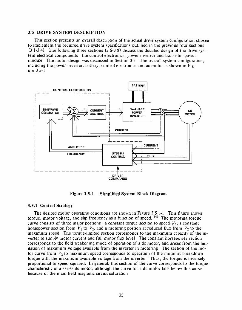
3.5 DRIVE SYSTEM DESCRIPTION
This sectIOn presents an overall descnptlOn of the actual dnve system configuration chosen to Implement the requlfed dnve system specificatIOns outlined In the prevIOus four sectIOns (3 1-34) The folloWIng three sectIOns (3 6-3 8) discuss the detailed design of the dnve system electncal components the control electronIcs, power Inverter and transistor power module The motor design was discussed In SectIOn 3 3 The overall system configuratIOn, IncludIng the power Inverter, battery, control electronICs and ac motor IS shown In Fig-ure 3 5-1
CONTROL ELECTRONICS I BATTERY I
I ---------------~ I 1 1 I I I I I 1
I I 1
1 1 I I 1-
~ SINEWAVE CURRENT GENERATOR CONTROL
~
" .I
/
AMPLITUDE
FREQUENCY
---------------
1 I I
'" 3-PHASE ,.....-f POWER ~
/ INVERTER 1
I 1
1 CURRENT
I - - - - - - /' 1 CURRENT
/' I
SYSTEM CONTROL ) I
if
" 1
- --~------' DRIVER
COMMANDS
FLUX
Figure 3.5-1 Simplified System Block Diagram
3.5.1 Control Strategy
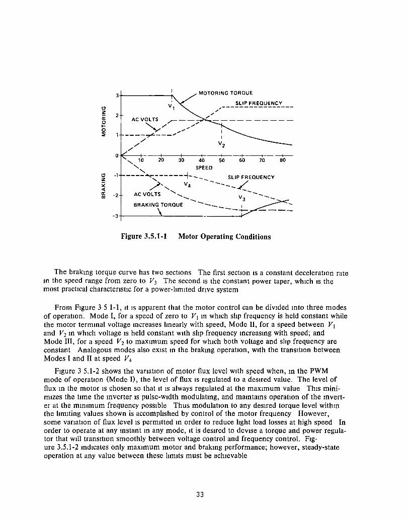
AC MOTOR
The deslfed motor operatIng conditions are shown In Figure 3 5 1-1 ThiS figure shows torque, motor voltage, and slip frequency as a functIOn of speed. (14) The motonng torque curve consists of three major portIOns a constant torque sectIOn to speed Vb a constant horsepower sectIOn from VI to Vb and a motorIng portIOn at reduced flux from V2 to the maximum speed The torque-limited sectIOn corresponds to the maximum capacity of the Inverter to supply motor current and full motor flux level The constant horsepower section corresponds to the field weakenIng mode of operation of a dc motor, and anses from the limItation of maXImum voltage available from the Inverter In motorIng The sectIOn of the motor curve from V2 to maXImum speed corresponds to operation of the motor at breakdown torque with the maXImum available voltage from the Inverter Thus, the torque IS Inversely proportIOnal to speed squared. In general, thiS sectIOn of the curve corresponds to the torque characteristic of a senes dc motor, although the curve for a de motor falls below thiS curve because of the maIn field magnetic CIrCUIt saturation
32
~ Z a:: o Io ~
~ z ~ < a: ell
J+------_+.. MOTORING TOROUE
2
0
-1
-2
-3
ACVOLTS ~ __
'v/ ........ "" ----7"'---"
/' /'
/'
SLIP FREQUENCY
I I ~--+-----+---+-- -----+-" 10 20 JO 40 50 60 70 80
" SPEED
---- ........ -------..,- SLIP FREQUENCY " -- .............. .,?', V4 ----L
ACVOLTS ........ , ---__ .............. _ V J -
BRAKING TORQUE - __
Figure 3.5.1-1 Motor Operating Conditions
The brakIng torque curve has two sectIOns The first sectIOn IS a constant deceleration rate In the speed range from zero to V3 The second IS the constant power taper, which IS the most practical charactenstIc for a power-lImited dnve system
From Figure 3 5 1-1, It IS apparent that the motor control can be diVided Into three modes of operatIOn. Mode I, for a speed of zero to VI In which slIp frequency is held constant while the motor termInal voltage Increases lInearly with speed, Mode II, for a speed between VI and V2 In which voltage IS held constant with slIp frequency IncreaSIng with speed; and Mode III, for a speed V2 to maximum speed for which both voltage and slIp frequency are constant Analogous modes also eXist In the brakIng operation, with the transItion between Modes I and II at speed V4
FIgure 3 5.1-2 shows the vanatIOn of motor flux level wIth speed when, In the PWM mode of operation (Mode I), the level of flux IS regulated to a desired value. The level of flux In the motor IS chosen so that It IS always regulated at the maximum value ThIS minimIzes the tIme the Inverter IS pulse-wIdth modulatIng, and maIntaInS operatIOn of the Inverter at the mInImUm frequency possIble Thus modulation to any desIred torque level withIn the lImiting values shown is accomplIshed by control of the motor frequency However, some vanatIOn of flux level IS permitted In order to reduce lIght load losses at high speed In order to operate at any Instant In any mode, It is desIred to devise a torque and power regulator that WIll tranSItIon smoothly between voltage control and frequency control. FIg-ure 3.5.1-2 IndIcates only maXImum motor and brakIng performance; however, steady-state operation at any value between these lImits must be achievable
33

3 +-------;.. V1
(;1 z 2 ------~ a: ,
',<", FLUX
I "
o I-o ~
PWM -,- SQUARE - ........ <:::: -WAVE ---___ _
o t------...-. ---+-. ----+---- --+-- -- - -+-- - - - -- - ---+--~ ~ ~ ~ ~ ro ~ 10
SPEED __ -
(;1 -1 1---__ PWM ---.J~I"_- SQUARE ~'---------.... z WAVE_-;::.-;;r-r-
:II: FLUX V4 ",,-i -2 ---_L __ ..v .... TORQUE
-3~----~---------~
Figure 3.5.1-2 Relative Torque and Flux
3.5.2 Current-Controlled PWM
In order to Implement the control strategy descnbed In SectIOn 3 5 1 and because the power Inverter wIll operate from a nomInally fixed dc source voltage, a PWM method to vary the motor voltage must be chosen. There are a number of PWM methods which could be used (9,18,19,20)
One method presently In wide use dates back to the ongInal paper of Schonung and Stemmler (I8) Figure 3 4 5-1 IS an IllustratIOn of the method of generatIng the Inverter sWitchIng waveforms and the resultant output voltage waveform across the motor line to neutral connectIOn This voltage waveform causes motor current npple which adds to the motor losses and reqUires extra Inverter current handling capability In addition, because the waveform IS a voltage waveform, a small Imbalance In the motor voltage, due to the small motor stator reSistance, can cause a relatively large current Imbalance In the motor current An Imbalance In phase voltages WIll translate to a motor frequency npple In the dc link, and SInce the motor frequency vanes from 0 to 500 Hz, any resonances In the dc lInk filter tend to be eXCited In additIOn, It IS possible to generate dc currents In the motor which will cause extra heatIng In the motor and torque npple In the motor output
All of these PWM methods(9,18,19,20) have In common two dIsadvantages The first, dIScussed above, that these methods are voltage control systems, the second, that a special tranSItion mode of operation InvolVIng the synchromzation of the reference waveform WIth the deslfed output waveform IS reqUired. The reqUirements that the waveforms have very little imbalance and a very small de offset Impose a reqUirement for a high degree of preCISIOn on the waveform generatIOn ThiS means that the control eleetrollics must preCIsely generate a waveform With a fairly smooth SInUSOIdal output The second problem anses when an Inverter output voltage greater than about 80% of maximum IS reqUired, as at high speed For
34
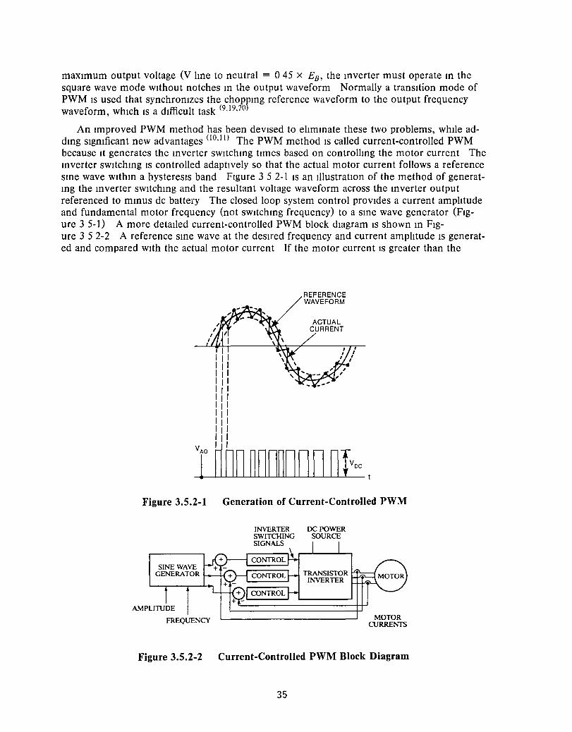
maXImum output voltage (V lIne to neutral = 045 X EB , the Inverter must operate m the square wave mode wIthout notches m the output waveform Normally a transItion mode of PWM IS used that synchronIzes the choppmg reference waveform to the output frequency waveform WhICh IS a dIfficult task (9,J9,20J ,
An Improved PWM method has been devIsed to elImInate these two problems, whIle addmg sIgnIficant new advantages 00,11) The PWM method IS called current-controlled PWM because It generates the mverter SWItchIng tImes based on controllIng the motor current The mverter SWItchIng IS controlled adaptIvely so that the actual motor current follows a reference sme wave withm a hysteresIs band FIgure 3 5 2-1 IS an IllustratIOn of the method of generatmg the mverter sWItchmg and the resultant voltage waveform across the mverter output referenced to mmus dc battery The closed loop system control prOVIdes a current amplItude and fundamental motor frequency (not SWItchIng frequency) to a SIne wave generator (FIgure 3 5-1) A more detaIled current-controlled PWM block dIagram IS shown m FIg-ure 3 52-2 A reference sme wave at the desIred frequency and current amplItude IS generated and compared WIth the actual motor current If the motor current IS greater than the
II II II II I I II II I I II II
REFERENCE WAVEFORM
II
T Joo ~OD~DD 0 O}oo I
Figure 3.5.2-1 Generation of Current-Controlled PWM
FREQUENCY
Figure 3.5.2-2
DC POWER SOURCE
MOTOR CURRENTS
Current-Controlled PWM Block Diagram
35
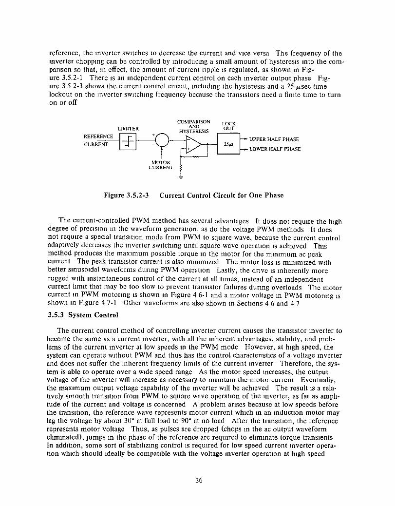
reference, the Inverter sWItches to decrease the current and VIce versa The frequency of the Inverter choppIng can be controlled by IntroducIng a small amount of hysteresIs Into the companson so that, In effect, the amount of current npple IS regulated, as shown In FIg-ure 3.5.2-1 There IS an Independent current control on each Inverter output phase FIgure 3 5 2-3 shows the current control ClfCUIt, IncludIng the hysteresIs and a 25 J1-sec tIme lockout on the Inverter SWItchIng frequency because the transIstors need a finIte tIme to turn on or off
REFERENCE
CURRENT
LIMITER
MOTOR CURRENT
LOCK OUT
UPPER HALF PHASE
LOWER HALF PHASE
Figure 3.5.2-3 Current Control Circuit for One Phase
The current-controlled PWM method has several advantages It does not requlfe the hIgh degree of preCISIOn In the waveform generatIOn, as do the voltage PWM methods It does not reqUlre a speCIal transItIon mode from PWM to square wave, because the current control adaptlvely decreases the Inverter SWItchIng until square wave operatIOn IS achIeved ThIS method produces the maxImum pOSSIble torque In the motor for the mInImum ac peak current The peak transIstor current IS also mInimized The motor loss IS minImized with better SInUSOidal waveforms durIng PWM operatIOn Lastly, the dnve IS Inherently more rugged with Instantaneous control of the current at all times, Instead of an Independent current hmlt that may be too slow to prevent transistor faIlures durIng overloads The motor current In PWM motonng IS shown In Figure 4 6-1 and a motor voltage In PWM motonng IS shown In FIgure 4 7-1 Other waveforms are also shown In SectIons 46 and 47
3.5.3 System Control
The current control method of controllIng Inverter current causes the tranSistor Inverter to become the same as a current Inverter, With all the Inherent advantages, stablhty, and problems of the current Inverter at low speeds In the PWM mode However, at high speed, the system can operate WIthout PWM and thus has the control charactenstIcs of a voltage Inverter and does not suffer the Inherent frequency hmlts of the current Inverter Therefore, the system is able to operate over a Wide speed range As the motor speed Increases, the output voltage of the Inverter Will Increase as necessary to maIntaIn the motor current Eventually, the maximum output voltage capablhty of the Inverter Will be achieved The result IS a relatively smooth transItion from PWM to square wave operatIOn of the Inverter, as far as am phtude of the current and voltage IS concerned A problem anses because at low speeds before the tranSItIon, the reference wave represents motor current which In an InductIOn motor may lag the voltage by about 30° at full load to 90° at no load After the tranSItion, the reference represents motor voltage Thus, as pulses are dropped (chops In the ac output waveform ehmInated), Jumps In the phase of the reference are reqUlred to ehmInate torque transients In additIOn, some sort of stablhzIng control IS reqUlred for low speed current Inverter operatIon which should Ideally be compatIble With the voltage Inverter operatIOn at high speed
36

Some known methods of controlling current mverters for motor stabIlity mclude some form of slip frequency control combmed wIth current regulatIOn when mductIOn motors are used, (21,22) or the well-known shaft posItIOn sensmg when synchronous motors are used Both these methods are dIfficult to use to handle the transItIon from current-controlled PWM to voltage control An alternatIve stabIlizmg control, SUItable for both current and voltage control, IS a method of motor electncal angle control applicable to both synchronous and mductIon motors (10,23) ThIS control method measures and regulates a modIfied angle between the motor's rotor flux vector and the stator (mverter) current vector (23)
Shown m FIgure 3 5 3-1 IS an example relatmg several motor angles to the motor slip frequency and torque for constant air gap flux operatIOn (23) The actual motor angle smO sm IS not monotontc, whIch would be undeSIrable for use as a feedback quantIty, and the angle mcludmg the rotor leakage flux smOsr has low gam for hIgh slips so regulatIOn would be poor A modIfied angle (smO) eq IS developed (23) WhIch IS actually used m the control system ThIS control method stabIlizes the dnve system m current mverter operatIOn (current-controlled PWM) and allows for a feedback-controlled transltton between current control and voltage control (square wave operatIOn) The sme wave reference generator (FIgure 3 5-0 phase angle WIll be vaned as pulses are dropped to mamtam the deSIred motor operatIon
Obtammg the motor angle (smO) eq mvolves measunng the stator currents and the aIr gap flux as vectors The aIr gap flux could be calculated from the termmal voltage but thIS IS not adequate at low frequency due to the voltage drop across the stator reSIstance DIrect measurement usmg air gap flux sensmg coIls wound around the stator teeth IS the preferred method and IS used for the actual system (17) The method of making and msertmg the sensmg COlIs WIthout dIsturbing the mam motor wmdmg was developed by General Electnc,06)
14
12
10 slNesr 2000
SINe 08 ---- 1600 ............ ......
......
" Te " 06 , 1200 , , , Te (ft-Ib) , 04
\ , 800 \
\ \
\ 02 \ 400
\ \ \
\ O~ ____ L-____ L-__ ~~ __ ~ ____ ~ ____ ~
0 10 8 6 4 2 0
f'l (Hz)
Figure 3.5.3-1 Induction Motor Angle and Torque as Function of Slip Frequency
37

Shown In Figure 3 5 3-2 IS a vector diagram of the stator voltage, stator current, and air gap flux linkage This diagram defines the relatIOnship of these quantities to each other along with a defillitIon of the machIne torque angle
d-AXIS
Iqso Vqso
q-AXIS 15 POWER FACfOR = cos d
= lqsohso
/we(sec- I )
d-q AXES ARE ROTATING AT THE INSTANTANEOUS ROTATIONAL SPEED OF THE APPLIED STATOR VOLTAGE
NOTE THE TORQUE ANGLE USED FOR FEEDBACK IS THE MODIFIED ANGLE BETWEEN THE STATOR CURRENT VECfOR AND ROTOR FLUX VECfOR (smfl)eq
Figure 3.5.3-2 Vector Diagram of Motor Operation
A block dIagram of the feedback sIgnal processIng of the motor current, flux, torque, angle and real component of stator current IS shown In FIgure 3 5 3-3 The InPl!.,t~ to the CIrcuIt are Vll1a , VlI1b , VII1c> the air gap voltages, and las' lbs' lcs the motor currents The CirCUIt performs an IntegratIOn of the air gap voltages to obtaIn flux t/J ma' t/J mb, t/J mc The a d-q aXIS multiplicatIOn (14) (see Appendix B) IS performed to calculate electrollic torque A refinement to a torque controller concept IS to dIVide the electrollic torque by the magllltude of flux wIth a small correctIOn for the magllltude of the stator current, YIeldIng the real component of stator current ThIS IS the actual feedback SIgnal, rather than torque, used In the outer loop of the control Further diVISIOn of the real component of stator current by the magllltude of current YIelds the deSired control angle (SInO) eq These Inputs and the angle are satisfactory for complete control of the dnve system, but do not allow for an eaSIly generated dnver command SIgnal The additIOn of two outer control loops (Figure 3 5 3-4), flux and real current, solve thiS problem Both of these feedback Signals are aVailable as by-products of the motor angle sensmg circuits Use of these Signals elimInates the need for a tachometer Figure 3 5 3-4 shows the addition of the angle control Inner loop and the flux and real current outer loops, along With the feedback Signal processmg, to the current-controlled PWM block dIagram
One of the outer loops chosen IS a real current regulator operatIng through the Inverter frequency Input because real current control can be mamtaIned In square wave operation and
38

PWM operation, smce frequency IS a vanable m both regIOns of operatIOn but voltage amplItude IS not In PWM operation it IS desirable to regulate the air gap flux at all speeds so the other outer loop IS a flux regulator operatmg through the mverter current amphtude mput
Vma Il'ma
d-q
Il'mb AXIS Te (SINB)eq
MUL TIPLlCA-
TION
Il'mc
Ill'ml-Kllsl Iisl
Figure 3.5.3-3 Feedback Signal Processing
MOTOR CURRENTS
FLUX FEEDBACK
SIGNAL )4--------~ PROCESSING '---
SIN8eq
REAL CURRENT COMMAND
REAL CURRENT
las Ibs MOTOR Ics CURRENTS
vma AIRGAP ~mb VOLTAGES
me
Figure 3.5.3-4 Overall Drive System Block Diagram
39
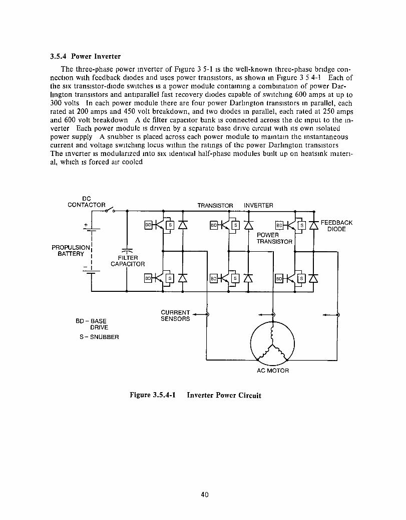
3.5.4 Power Inverter
The three-phase power mverter of FIgure 3 5-1 IS the well-known three-phase bndge connectIOn wIth feedback dIOdes and uses power transIstors, as shown m FIgure 3 5 4-1 Each of the SIX transIstor-dIode sWItches IS a I?ower module contammg a combmatIOn of power DarlIngton transIstors and antIparallel fast recovery dIOdes capable of sWItchmg 600 amps at up to 300 volts In each power module there are four power DarlIngton transIstors m parallel, each rated at 200 amps and 450 volt breakdown, and two dIOdes m parallel, each rated at 250 amps and 600 volt breakdown A dc filter capacItor bank IS connected across the dc mput to the mverter Each power module IS dnven by a separate base dnve CIfCUIt WIth ItS own Isolated power supply A snubber IS placed across each power module to mamtam the mstantaneous current and voltage sWItchmg locus wIthm the ratmgs of the power DarlIngton transIstors The mverter IS modulanzed mto SIX IdentIcal half-phase modules bUllt up on heatsmk matenaI, WhICh IS forced aIr cooled
DC
CONT:rOR~
-II
PROPULSION: BATIERY I F~R
I CAPACITOR .::..L
BD- BASE DRIVE
S- SNUBBER
TRANSISTOR INVERTER
POWER TRANSISTOR
AC MOTOR
Figure 3.5.4-1 Inverter Power Circuit
40
FEEDBACK DIODE
-

3.6 CONTROL ELECTRONICS
The control electromcs hardware IS shown m Figure 3.6-1. The card cage IS a 438 x 368 x 191 cm (173 x 14.5 x 75 m) enclosure welghmg 6.4 kg (14.2 lb) There are eight control cards Note the external connectIOns to the motor and power mverter. Note also the dnver command module next to the card cage.
The overall dnve system block diagram of Figure 3.5 3-4 IS expanded m detaIl and the eight control cards with their functIOns are blocked out m Figure 36-2. A detaIled descnptIOn of operatIOn for each control card IS given m Appendix B The indiVidual control card drawmgs are m Appendix D
ThiS sectIOn presents the functIonal design and operatIOn of the control electromcs for the ac controller. ThiS descnptIOn IS more detaIled than that presented m SectIon 3 5.3, but not as detailed as the mdlvldual control card descnptlons m Appendix B The signal conventIOns used when dlscussmg signals on the control cards are defined m SectIOn 7 The followmg sectIons refer to the control functIon block diagram shown in Figure 3 6-3 The control electronICS schematIc (EP7644 MCEA) m Appendix D may also be useful m reference to the followmg diSCUSSion
41

Figure 3.6-1. Control Electronics Assembly and D:rlver Command Module

Zero Speed Detector
CPRA
Figure 3.6-2
Driver Command & Jerk Limit
CDCA
Shutdown Driver (SO) Commands
Control Circuit Card Block Diagram
Current Interface & Summing
CIIA & CTOA
Torque
CTOA
Note: The letters in the blocks refer to the last four letters of the individual control card drawings in Appendix D.
43

~ ~
ACC
BRAKE
DIR·
MOTOR STATOR
CURRENTS
ON/OFF DRIVER COMMAND AND
JERK LIMIT
NOTE P = PROPORTIONAL I = INTEGRAL D = DERIVATIVE XD = CURRENT TRANSDUCER CT = CURRENT TRANSFORMER
LO = LOCKOUT SEP = SEPARATOR MEANS COMMAND SIGNAL F/R = FORWARD/REVERSE SIGNAL
Figure 3.6-3
I" Ie Ie
(a)
F/R
f\j\ RA AU AL
N RB BU i
TRANSISTOR BASE
Ie
BL DRIVE
III IV\; RC
SIGNALS
CU CL
MICR'OPROcEsSOR SINE WAVE
GENERATOR
(b)
Control Function Block Diagram
a. Feedback Signal Processing Block Diagram
b. Closed Loop Controls Block Diagram

3.6.1 Current Control Loop
The current control loop compares the actual three-phase motor currents (lA, IB, IC) to a three-phase SIne wave reference (RA, RB, RC) to produce the phase sWItchIng commands (lA COMO, IB COMO, IC COMO) WhICh determIne when to sWItch the power transIstor modules (reference FIgure 3 6-3b) Instantaneous current lImIt IS Inherent In thIS technIque SInce the actual current IS always beIng controlled dIrectly
The motor current feedback sIgnals enter the control electrOnIcs at two POInts (reference FIgure 3 6-3a) The outputs of the Hall-effect current transducers (XO's) are brought In through connector P3 to the transducer Interface card (EP7644CTIA), WhICh also provIdes the calIbrated bIaS currents to the transducers The outputs of thIS card (lAl, IBl, IC1), are negatIve In SIgn and scaled to 100 amps/volt The outputs of the current transformers (CT's) enter the control electrOnIcs through connector Pll, and then to the torque card (EP7644CTQA) where they are scaled to 80 amps/volt (lA2, IB2, IC2) The current transducers have lImIted hIgh frequency response and are low-pass filtered (below 400 Hz) and rescaled to 80 amps/volt on the torque card to proVIde the dc component of the current. The current transformer sIgnals are hIgh-pass filtered (above 400 Hz), and proVIde the pnncIpal component of the current feedback The two sets of sIgnals are summed on the torque card to generate compOSIte motor current feedback sIgnals (lA, IB, IC), and are aVaIlable at test POInts on the edge of the torque card
The phase current reference waveforms (RA, RB, RC) are filtered on the protectIon card (EP7644CPRA) and compared to the current feedback sIgnals (lA, IB, IC) to generate the phase current command sIgnals (lA COMO, IB COMO, IC COMO) as shown In FIgure 3 6-3b. These are passed to the lockout card (EP7644CLOA) where a lockout functIon IS applIed to force a penod of tIme between one power module's turn otT and the complementary power module's turn on ThIS prevents overlap of the power modules' conductIOn tImes to prevent a "shoot-thru", a condItIon WhICh would occur If a contInuous path eXIsted through both power modules In the same phase caUSIng a hIgh-fault current WhICh would destroy the two power modules Involved IA COMO, IB COMO, and IC COMO are then split Into upper and lower power module dnve commands (AU, AL, BU, BL, CU, CL) whIch are sent to the base dnver modules (EP7644MBOA) In the power Inverter assembly through coaxIal cables The base dnver modules are optIcally coupled at the Input and are deSIgned to source base current to the power modules when current IS flOWIng at the Input and to SInk base current from the power modules when Input current IS not flowmg The current sink mode of operatIon IS Intended to sweep out stored charge from the base JunctIons of the power modules for fast turn off.
The phase current reference waveforms (FIgure 3 6-3b) are three SInUSOIdal waveforms separated by 120 electncal degrees whose amplItude IS controlled by Ilr and whose frequency IS controlled by FREQ* and are produced by the reference generator portIon of the lockout card (EP7644CLOA) The reference generator conSIsts pnmanly of a microprocessor, three dIgital-to-analog (0/ A) converters, and a voltage-to-frequency (V /F) converter The microprocessor computes the relattve amphtudes of the three waveforms at a smgle pomt in the penod and sends the results to three 0/ A converters where they are multIplied by IIr (the amplitude control SIgnal) to set the peak amplItude of the waveforms FREQ* (the frequency control signal) is converted by the V /F converter to a pulse train whose frequency is proportional to the deSIred frequency of the waveforms. This pulse train clocks the reference generator, caUSIng It to compute succeSSIve sets of values of the waveforms. The result is three SInUSOIdal waveforms WIth dIscrete "staIrcase" values WhICh then must be filtered as dIScussed In the previous paragraph.
45

The amplitude and frequency of the reference current waveforms are controlled by the two Inputs ~I~ and FREQ*) to the reference generator, whIch are determIned by the outer loop controls of the ac controller
3.6.2 Outer Loop Controls
3.6.2.1 Flux regulator
The flux regulator controls the flux In the motor by varyIng the amplitude of the reference generator USIng ilr as shown In FIgure 3 6-3b ThIs controls both the ImagInary component of current whIch generates flux and the real component whIch generates torque, as shown In FIgure 3 6 2 1-1 SInce the angle regulator controls the real component of current OREAL) by varymg the shp angle () (to be dIscussed m a later sectlOn), the flux regulator IS reqUlred to compensate for changes m the ImagInary component of current caused by the angle regulator and VIce versa To aVOId unstable mteractlOn, the flux control loop IS a much slower loop
IIMAG (FLUX)
TAPERING OF FLUX LEVEL AT LOW : ____ ~:::::::.:: __________ ~-;:.Qu-=- -i II
I -........-........ _:.--- I I -- I I I I I I I I I : (lREAL = I I I SIN 0) I
REGENERATIVE - BRAKING
MOTORING-
IREAL (TORQUE)
Figure 3.6.2.1-1 Imaginary and Real Components of Current
The atr gap flux m the motor IS sensed by three pam of wmdmgs, two wmdmgs per phase Smce there are no motor pole faces dIrectly m phase wIth the current, the nearest pole faces are 15 degrees early and 15 degrees late Therefore, there IS one coll on each pole face and the two are connected m senes (FIgure 362 1-2a), YIeldmg a vector summatlOn of the two SIgnals (FIgure 362 1-2b) whIch IS m phase wIth the current The flux COIl voltage SIgnals (VMA, VMB, VMC) are mtegrated to obtam the flux Signals (FLUXA, FLUXB, FLUXC) as shown m FIgure 36-3a These are then rectified and summed to obtam iFLUXi The command for the flux regulator (iFLUXi*) IS obtamed from a functlOn generator which sets a mmlmum value when no torque IS bemg requested (Figure 3 62 1-1 and Figure 3 6-3b) AdditlOnal flux IS commanded at higher torque and IS obtamed by mcreasmg iI~ proportlOnately until maximum flux IS commanded A limIt functlOn IS applied to into so that the controller cannot command more than the maximum current that the power modules can handle
An addItional mput to the flux regulator senses any abrupt mcrease m commanded torque and qUickly boosts iI~ Via a denvatIve of sm()* until the flux regulator, which has an mherently slow response, can catch up (Figure 3 6-3b) ThIS Will be dIscussed further m the sectlOn concernmg the real current regulator
46

--~~--------~~~VMB ---
(A) (8)
Figure 3.6.2.1-2 Flux Coil Configuration
a. Flux Coil Connections
b. Flux Coil Vector Diagram
3.6.2.2 Angle regulator
The mam loop for controllIng motor torque IS the angle regulator ThIS regulator controls the frequency of the applIed stator current waveforms by way of the frequency control mput to the reference generator (FREQ*) If the frequency of the stator current waveforms IS equal to the rotatmg frequency of the motor, no current IS mduced m the rotor, 1 e , an alternatmg current of zero frequency and zero amplItude (zero slIp) The rotor Impedance becomes reslstlve m nature smce the reactlve component IS zero Therefore, there will be zero angle between the rotor current phasor and the rotor voltage phasor ThIS angle IS the slip angle and determmes the torque of the motor As slIp mcreases, 1 e , the difference between the applied stator frequency and the rotatmg frequency, the frequency of the rotor current mcreases ThiS produces an angle between the rotor current phasor and the rotor voltage ph asor which mcreases WIth mcreasmg slip due to the rotor's reactlve Impedance causmg mcreasmg torque An applied frequency greater than rotatmg frequency wIll produce a posltlve or acceleratmg torque Conversely, an applied frequency less than rotatmg frequency WIll produce a negatlve or brakmg torque The angle regulator, therefore, controls the slip angle by mcreasmg or decreasmg frequency as reqUired by ItS mputs, angle command (SIN 0*), and angle feedback (SIN 0), as shown m Figure 3 6-3b
3.6.2.3 Real current regulator
At the zero slIp condition, the stator current lIes essentially along the Imagmary aXIs smce the Impedance of the stator IS nearly pure reactance and no current IS flowmg by mutual mductance to the rotor The stator current phasor will therefore lag the stator voltage phasor by 90 degrees and will generate motor flux only
The real current regulator controls the real aXIS component of the stator current (Fig-ure 3 62 1-1), which IS the component whIch generates torque The Imagmary aXIS component of the stator current IS the component which generates flux When no torque IS bemg
47

generated, the stator current phasor lies along the Imagmary aXIS, generatmg only flux, and the real aXIs component IS zero When torque IS reqUired, the command appears as a request for the real component of stator current OREAL *) as shown m Figure 3 6-3b A posItive value of IREAL * will cause a positive value of the real current regulator output (SIN (J*) m order to command a pOSItive torque angle This, m turn, Will cause an mcrease m frequency through the angle regulator to create the posItive torque angle As the angle mcreases, the flux regulator must respond with an mcrease m total current QIr) m order to regulate the motor flux Smce the flux regulator cannot qUickly respond with an mcrease m total current, the flux m the motor Will tend to decrease momentanly This IS compensated by usmg the denvatIve of SIN (J* to boost IIr until the flux regulator can catch up, as discussed earlier
As speed mcreases, the motor Will reqUire more output voltage to generate a given flux level When the mverter can no longer mcrease the output voltage, havmg reached the full square wave voltage, the flux regulator will lose control and the flux will begm to fall off The angle regulator Will respond with an mcrease m angle to regulate the real component of current OREAL), as shown m Figure 3 623-1 This automatically creates a tranSitIOn from the constant torque regIOn of operation to the constant horsepower regIOn
-----------------1 flO = INCREASED ANGLE TO REGULATE IREAL AND FLUX AT HIGH SPEED
III
I I I I 1
I I I REDUCTION AT HIGH SPEED TO LIMIT FLUX LEVEL
-------- --------1
Figure 3.6.2.3-1
3.6.3 Motor Reversing
I 1
I I I I
1 REGULATED VALUE OF IREAL
Regulation of Real Component of Current
To change the dIrectIOn of rotatIOn of an mductlOn motor, the phase sequence of the power applied to the motor must be reversed For operatIOn from a fixed power system, thiS IS accomplished by sWltchmg two of the motor's power leads by means of a contactor When operatmg from an mverter such as used on thiS dnve, the reversal can come from the mverter Itself by reversmg the phase sequence of the transistor finng ThiS IS eaSily accomplished by means of the sme wave reference generator (Figure 3 6-3b)
48
The mIcroprocessor IS programmed to accept a dIrectIOn sense sIgnal and wIll produce the reverse phase sequence when commanded The output frequency can be programmed to zero wIth a phase sequence of A,B,C, and can be restarted havIng the OpposIte sequence of A,C,B ThIs reversal IS sent to the transIstor base drIve CIrCUIts caUSIng the Inverter to change phase sequence and reverSIng the motor dIrectIOn Thus, motor reverSIng IS Incorporated In the basIc desIgn
AddItIonal controls need to be added to ensure the proper COndItIonS prIor to allOWIng reverse mode from a vehIcle safety standpOInt Also, an upper lImIt on the maXImum speed In reverse, e g , 24 km/h (15 mph), IS desIrable from a vehIcle safety consIderatIOn
The drIve Itself can be protected from adverse operatIOn by applYIng a maXImum rate-ofchange lImIt to the SIne wave reference generator, coupled wIth a current lImIt (power) to modIfy the control for cases of descendIng grades and SImIlar SItuatIOns
3.6.4 Other Functions
There are many other necessary functIOns bUIlt Into the control electrOnIcs The conventIOnal drIver commands of accelerator and brake pedals, duectIOn selectIOn, and IgnItIon sWItch must all be SImulated A Jerk lImIt functIOn operates on the accelerator and brake commands to slow down theIr rate-of-change A system of shutdown and reset SIgnals to approprIate control cards IS necessary for the InItIal startup, protectIOn durIng operatIon, and shutdown of the drIve system The drIve system also mOnItors several other condItIons as part of ItS protectIOn system lOgIC power supply voltage, lOgIC card Interlock, power module heatsInk overtemperature, dc overvoltage and dc undervoltage, and others All of these other functIOns are dIscussed In detaIl In the IndIVIdual control card deSCrIptIOn of operatIon (AppendIX B)
3.6.5 Control Performance
The transfer functIOns of the three loops, angle, flux and torque, are shown In SectIOn 4.3 They show the magnItude and phase response of the loop versus frequency
The flux level for the motor and the flux versus torque functIOn (FIgures 3 6-3b and 36.2 1-1) must be determIned The flux level IS determIned and the control cards calIbrated as shown In SectIOn 44 The flux-torque functIOn block IS programmed accordIng to the results presented In SectIOn 4.5 ThIS flux program results In an optImIzed motor effiCIency, because flux IS reduced at low torque levels to better balance the motor magnetIc and I2R loss The waveform of the air gap voltage IS shown In FIgures 47-2 and 47-5
The calculatIOns of IREAL and SInO from the feedback SIgnals and the d-q aXIS calculatIon of torque are shown In SectIOn 49 Also presented In SectIOn 49 are the relatIOnshIps of varIOUS control SIgnals to torque
The performance of the complete drIve system IS Illustrated In SectIOns 49 and 4.12 These are torque-speed and strIP chart recordIng presentatIOns of the system operatIon, respecttvely The drtve system performance recordmgs (Section 4 12) show the measured torque and speed, along with several control SIgnals of Interest.
49
3.7 POWER INVERTER
The power mverter hardware IS shown m FIgure 3 7-1 wIth the protectIve cover mstalled, and m FIgure 3 7-2 wIthout the cover ThIS engmeermg model power mverter IS 97 cm (38 m) x 66 cm (26 m ) x 20 cm (8 m ) and weIghs 59 kg (130 lb) There are SIX IdentIcal half-phase modules, whIch are descrIbed m SectIon 3 7 2 Note the dc filter capacItor bank down the mIddle of the mverter The hall effect current transducers, current transformers, and lIne fuses for each output phase are VISIble m the foreground of FIgure 3 7-2 The blowers for coolIng the half-phase module heatsmks are on the rIght end of the mverter
The power mverter CIrCUIt IS shown m SImplIfied form m FIgure 3 7-3 and m full detaIl m drawmg EP7644MIVA (AppendIx D)
The power Inverter has three major technIcal functIOns
• Interface between the storage battery and InductIOn motor dUrIng normal operatIOn dUrIng both motorIng and regeneratIve brakmg
o ProVIde the capabIlIty of controllIng the developed motor torque (both motorIng and regeneratIve brakIng) by adJustmg the applIed motor current, voltage, and frequency
• ProVIde the capabIlIty to protect Itself agamst abnormal condItIons such as overloads, short CIrCUIts, temperature extremes, and reversed battery connectIOns
3.7.1 Power Circuit
The power CIrCUIt configuratIOn IS the well-known three-phase brIdge connectIOn (29)
Three-phase ac power IS supplIed to the ac motor Each phase of the Inverter acts as a SIngle pole double throw SWItch connected to eIther the pOSItIve or common SIde of the dc bus The SWItches are bIlateral they can carry current In both dIrectIOns, USIng the tranSIstor for forward current and the antI parallel feedback dIOde for reverse current The dIodes carry the power factor related motor current as well as the bulk of the regeneratIOn current Due to the motor laggIng power factor, the bIlateral SWItches must be capable of forced commutatIOn
The pulse-WIdth-modulated (PWM) approach was chosen for the motor voltage control because
• The electrIC vehIcle drIve has a fixed dc bus voltage establIshed by the battery and IS well SUIted for PWM
• Other approaches USIng a regulated dc bus WIth an Input converter have more power level semIconductors, reqUIre an Inductor/capacItor dc filter, and regeneratIOn IS dIfficult
• The regeneratIOn WIth PWM IS Inherent and only a small dc capaCItor filter IS needed
• The power SWItches are utIlIzed for InVerSIOn and voltage control, IncreaSIng theIr contrIbuted value
• No large, heavy Inductors are reqUIred, as In some current-source approaches
• The generatIOn of complex PWM waveforms IS easIly accomplIshed WIth mIcroelectronIC controls
The chOIce of tranSIstors over thYrIstors was made because.
• The tranSIstors obVIate the need for costly and heavy thYrIstor commutatIOn CIrCUIts that are needed for forced commutatIOn
50
Figure 3.7-1 Power Inverter with Cover Installed

Ul N
DC FILTER
CURRENT TRANSFORMER
Figure 3.7-2 Power Inverter Without Cover
WER
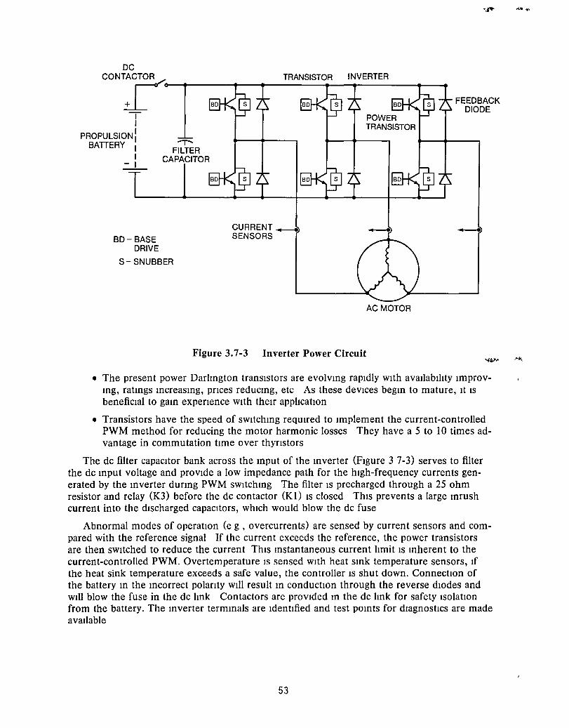
DC
CONT:rOR ,/, -I
I
PROPULSION: BATTERY I F~R
I CAPACITOR ~
BD- BASE DRIVE
S- SNUBBER
TRANSISTOR INVERTER
POWER TRANSISTOR
AC MOTOR
Figure 3.7-3 Inverter Power Circuit
FEEDBACK DIODE
-
• The present power DarlIngton transistors are evolving rapidly with availabilIty ImprovIng, ratings increaSing, pnces redUCing, etc As these deVices begin to mature, It IS beneficial to gain expenence With their applIcation
• Transistors have the speed of SWitching reqUired to Implement the current-controlled PWM method for reducing the motor harmonic losses They have a 5 to 10 times advantage in commutation time over thynstors
The dc filter capacitor bank across the Input of the Inverter (Figure 3 7-3) serves to filter the dc Input voltage and prOVide a low impedance path for the high-frequency currents generated by the Inverter dunng PWM SWitching The filter IS precharged through a 25 ohm resistor and relay (K3) before the dc contactor (Kl) IS closed This prevents a large Inrush current into the discharged capaCitors, which would blow the dc fuse
Abnormal modes of operatIOn (e g , overcurrents) are sensed by current sensors and compared with the reference signal If the current exceeds the reference, the power transistors are then SWItched to reduce the current ThIS Instantaneous current lImit IS Inherent to the current-controlled PWM. Overtemperature IS sensed With heat Sink temperature sensors, If the heat sink temperature exceeds a safe value, the controller IS shut down. ConnectIOn of the battery In the Incorrect polanty Will result In conductIOn through the reverse dIodes and Will blow the fuse in the dc link Contactors are proVided In the dc lInk for safety IsolatIOn from the battery. The Inverter terminals are Identified and test POints for dIagnostics are made available
53
3.7.2 Inverter Switching Frequency
A problem that must be faced IS the maXImum operatmg frequency of the mverter, WhICh IS determmed by the current-controlled PWM choppmg at low speeds The mverter sWltchmg losses are proportIOnal to frequency and must be controlled, thus the choppmg frequency should, on the average, be lImtted The rate of change of current and thus the choppmg frequency IS automatIcally controlled by the comparator hystereSIs, the motor stator plus rotor leakage mductance, and the dc lInk voltage by the equatIOn
EB-Emsmwt
Leq
WhICh, however, apphes only approXImately smce the motor leakage mductance IS a funchon of frequency and the voltage IS actually the dc hnk voltage mmus the motor back emf
WIth the three-phase mverter shown m FIgure 3 7-3 and three-wIre wye motor, there IS no neutral connectIOn Thus, the operatIOn of the mverter IS constramed because the sum of the three Ime currents must be zero at all mstants,
la + Ib + Ie = 0
The current m anyone phase IS completely determmed by controlhng the currents m the other two phases, rendermg one phase of a current controller redundant The sWItches of one phase cannot, however, be removed and the ClfCUlt sImphfied because the conventIOnal three phase configuratIOn IS more effiCIent under square wave operatIOn at hIgh speed
When the three phase mverter ClfCUlt of FIgure 3 7-3 WIthout a neutral connectIOn IS controlled by three IdentIcal current controllers, It can be expected that the mherent redundancy should affect the operatIOn m some manner that preserves symmetry between the phases ThIS IS seen m the waveforms obtamed from the actual dnve system m SectIOn 4 6 The actual current choppmg m FIgure 46-1 IS observed to dlmlmsh to very low frequency tWIce per cycle on each phase for a penod of about 60 0 The current for thIS phase IS bemg mamtamed wlthm the hysteresIs band by the choppmg on the other two phases Thus, the average choppmg frequency IS lower than expected The portIOn of the losses that depend on the current are sIgmficantly less when the power factor IS near umty, because the peak current WIll occur m the vlcmlty of the peak counter emf WIth whIch the penod of low choppmg frequency comcldes The frequency spectrum (fIgure 4 6-2) of thIS current shows the choppmg frequency IS spread over a range of 500 to 4500 Hz FIgure 4 6-5 IS the motor current waveform dunng PWM operatIOn m regeneratIOn The choppmg IS nearly umform over the cycle, unlIke motonng, becasue the counter emf IS low The frequency spectrum (FIgure 4 6-6) shows a nearly constant 43kHz choppmg frequency These choppmg frequencIes are slIghtly hIgher than the deSIgn specIficatIOns, but are acceptable
3.7.3 Inverter Packaging
The baSIC mverter packagmg block IS the half-phase module shown m FIgure 3 7 3-1 and drawmg EP7644MPHA (AppendIX D) ThIS module contams the power module, snubber, base dnve, base dnve power supply, overtemperature sensor, and thermocouple (under the, power module, part of the test mstrumentatIOn) All of these deVIces are mounted on a length of heatsmk extrusIOn matenal The three modules common to the upper dc raIl are one half of the mverter and share the same blower, whIle the other three form the other half and share the other blower The blowers operate from the mam dc bus
54

Figure 3.7.3-1 Half-Phase Module
The inverter is cooled with forced air and is specified to operate in a 239 K (- 30 OF) to 322 K (+ 120 OF) ambient. The approximate air flow required can be calculated from the equation:
F= 1.76 P
Tout - Tin
where,
F = air volume flow in ft3 I min
P = heat load in watts
Tout = Exhaust temperature in K
Tin = Inlet temperature in K
At full power (41 hp) the 7080 13/min (250 ft3/min) blowers will hold about a 25 K rise on the heatsinks.
The entire inverter is covered by an aluminum mesh cover. This provides personnel safety, yet adequate convection cooling. The half-phase modules are insulated from the inverter aluminum chassis. All other components are mounted to this chassis. The current transducers and transformers are contained in their own assemblies and are bolted to the inverter chassis.
3.7.4 Power Darlington Transistor Base Drive
Both bases, Bl and B2, of the power Darlington transistor are driven. Bl is the base of the npn driver transistor and B2 is the base of the npn output transistor. Figure 3.7.4-1
55
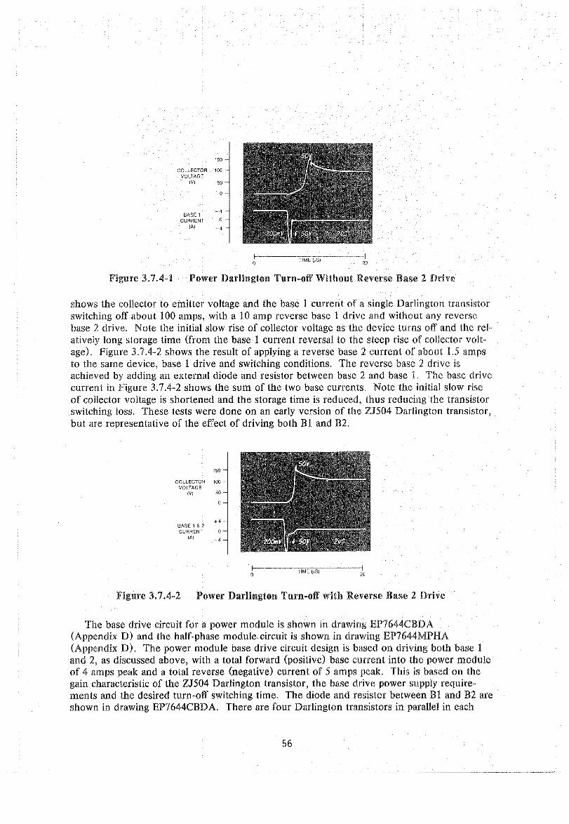
150
COLLECTOR 100 VOLTAGE
(V) 50
O·
BASE 1 +4
CURRENT (AI -4
20
Figure 3.7.4-1 Power Darlington Tum-off Without Reverse Base 2 Drive
shows the collector to emitter voltage and the base 1 current of a single Darlington transistor switching off about 100 amps, with a 10 amp reverse base 1 drive and without any reverse base 2 drive. Note the initial slow rise of collector voltage as the device turns off and the reI·· atively long storage time (from the base 1 current reversal to the steep rise of collector voltage). Figure 3.7.4-2 shows the result of applying a reverse base 2 current of about 1.5 amps to the same device, base 1 drive and switching conditions. The reverse base 2 drive is achieved by adding an external diode and resistor between base 2 and base 1. The base drive current in Figure 3.7.4-2 shows the sum of the two base currents. Note the initial slow rise of collector voltage is shortened and the storage time is reduced, thus reducing the transistor switching loss. These tests were done on an early version of the ZJ504 Darlington transistor, but are representative of the effect of driving both BI and B2.
150
COLLECTOR 100 VOLTAGE
(V) 50·
+4 BASE 1 & 2 CURRENT 0-
(A) -4
Figure 3.7.4-2 Power Darlington Tum-off with Reverse Base 2 Drive
The base drive circuit for a power module is shown in drawing EP7644CBDA (Appendix D) and the half-phase module. circuit is shown in drawing EP7644MPHA (Appendix D). The power module base drive circuit design is based on driving both base I and 2, as discussed above, with a total forward (positive) base current into the power module of 4 amps peak and a total reverse (negative) current of 5 amps peak. This is based on the gain characteristic of the ZJ504 Darlington transistor, the base drive power supply requirements and the desired turn-off switching time. The diode and resistor between HI and B2 are shown in drawing EP7644CBDA. There are four Darlington transistors in parallel in each
56
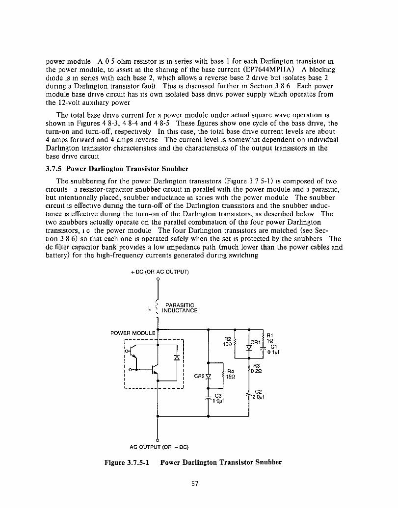
power module A 0 5-ohm resistor IS In series with base 1 for each Darlington transistor In the power module, to assist In the shanng of the base current (EP7644MPHA) A blocking dIOde IS In senes with each base 2, which allows a reverse base 2 dnve but Isolates base 2 dunng a Darlington transistor fault This IS discussed further In SectIOn 3 8 6 Each power module base dnve CircUit has ItS own Isolated base dnve power supply which operates from the 12-volt auxiliary power
The total base dnve current for a power module under actual square wave operatIOn IS shown In Figures 4 8-3, 4 8-4 and 4 8-5 These figures show one cycle of the base dnve, the turn-on and turn-off, respectively In this case, the total base dnve current levels are about 4 amps forward and 4 amps reverse The current level IS somewhat dependent on individual Darlington transistor charactenstlcs and the charactenstlcs of the output transistors In the base dnve CIfCUIt
3.7.5 Power Darlington Transistor Snubber
The snubbenng for the power Darlington transistors (Figure 3 7 5-0 IS composed of two CircUits a resistor-capacitor snubber CircUit In parallel with the power module and a parasitiC, but intentIOnally placed, snubber Inductance In senes with the power module The snubber CircUit IS effective dunng the turn-off of the Darlington transistors and the snubber inductance IS effective dunng the turn-on of the Darlington transistors, as descnbed below The two snubbers actually operate on the parallel combinatIOn of the four power Darlington tranSistors, I e the power module The four Darlington transistors are matched (see Sec-tIOn 3 8 6) so that each one IS operated safely when the set IS protected by the snubbers The dc filter capacitor bank provides a low Impedance path (much lower than the power cables and battery) for the high-frequency currents generated dunng sWitching
+ DC (OR AC OUTPUT)
] " PARASITIC
L :. INDUCTANCE
POWER MODULE
I I : ~---l. I I I '---------
-----1 I I I I I I I I I I ____ J
AC OUTPUT (OR - DC)
CR2
R2 10Q
R4 15Q
R1 CR1 1Q
C1
R3 02Q
o 1flf
Figure 3.7.5-1 Power Darlington Transistor Snubber
57
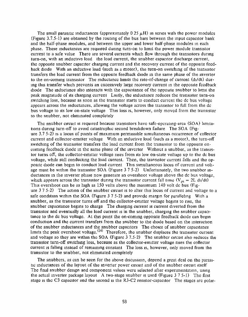
The small parasItic Inductances (approxImately 0 25 JLH) In senes wIth the power modules (FIgure 3.7.5-1) are obtamed by the routIng of the bus bars between the mput capacItor bank and the half-phase modules, and between the upper and lower half-phase modules m each phase. These mductances are reqUIred durmg turn-on to hmlt the power module transIstor current to a safe value There are several currents WhICh flow through the transIstors dUrIng turn-on, WIth an mductIve load the load current, the snubber capacItor dIscharge current, the OpposIte snubber capacItor chargmg current and the recovery current of the OpposIte feedback dIOde WIth an mductIve load (such as a motor), the turn-on sWItchmg of the transIstor transfers the load current from the OpposIte feedback dIOde m the same phase of the mverter to the on-commg transIstor The mductance hmlts the rate-of-change of current (dl/dt) durIng thIS transfer WhICh prevents an excessIvely large recovery current m the OpposIte feedback dIOde The mductance also mteracts WIth the capacItance of the OpposIte snubber to hmlt the peak magmtude of ItS chargmg current Lastly, the mductance reduces the transIstor turn-on sWItchmg loss, because as soon as the transIstor starts to conduct current the dc bus voltage appears across the mductances, allowmg the voltage across the transIstor to fall from the dc bus voltage to ItS low on-state voltage ThIS loss IS, however, only moved from the transIstor to the snubber, not ehmmated completely
The snubber CIrCUIt IS reqUIred because transIstors have safe-operatmg-area (SOA) limItations dunng turn-off to aVOId catastrophIc second breakdown faIlure The SOA (FIg-ure 3.7 5-2) IS a locus of pomts of maXImum permISSIble SImultaneous occurrence of collector current and collector-emItter voltage WIth an mductIve load (such as a motor), the turn-off sWItchmg of the transIstor transfers the load current from the transIstor to the OpposIte oncommg feedback dIOde m the same phase of the mverter WIthout a snubber, as the transIStor turns off, the collector-emItter voltage nses from ItS low on-state voltage up to the dc bus voltage, whIle still conductmg the load current. Then, the transIstor current falls and the oppOSIte dIOde can begm to conduct load current ThIS SImultaneous locus of current and voltage must be wlthm the transIstor SOA (FIgure 3 7 5-2) Unfortunately, the two snubber mductances m the mverter phase now generate an overshoot voltage above the dc bus voltage, whIch appears across the transIstor durmg the transIstor current fall tIme (V pk = 2L dll dt) ThIS overshoot can be as hIgh as 150 volts above the maXImum 140 volt dc bus (FIg-ure 3 7 5-2) The actIOn of the snubber CIrCUIt IS to alter thIS locus of current and voltage to a safe condItIOn wlthm the SOA (FIgure 3 7 5-2) and provIde margm for parallehng WIth a snubber, as the transIstor turns off and the collector-emItter voltage begms to nse, the snubber capacItance begms to charge The chargmg current IS current dIverted from the transIstor and eventually all the load current IS in the snubber, chargmg the snubber capaCItance to the dc bus voltage. At thIS pomt the on-commg OpposIte feedback dIode can begm conductIOn and the current transfers from the snubber to the dIOde based on the mteraction of the snubber mductances and the snubber capacItors The chOIce of snubber capacItance hmits the peak overshoot voltage. (24) Therefore, the snubber dIsplaces the transIstor current and voltage so they are wlthm the SOA (Figure 3 7.5-2) The snubber ClfCUIt also reduces the transIstor turn-off sWItchmg loss, because as the collector-emItter voltage nses the collector current IS falhng mstead of remammg constant The loss IS, however, only moved from the tranSIstor to the snubber, not elImmated completely
The snubbers, as can be seen for the above dISCUSSIOn, depend a great deal on the paraSItic mductances of the layout of the mverter power CIrCUIt and of the snubber ClfCUlt Itself The final snubber deSIgn and component values were selected after expenmentatIOn, usmg the actual mverter package layout A two-stage snubber IS used (FIgure 3 7 5-1) The first stage IS the C3 capacItor and the second IS the R3-C2 reSIstor-capacItor The stages are polar-
58
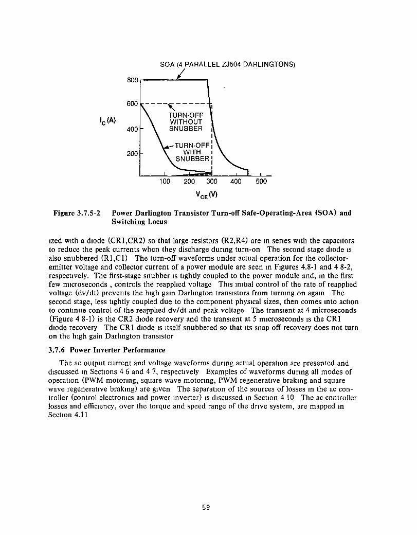
SOA (4 PARALLEL ZJ504 DARLINGTONS)
Ie (A)
800~----~-----,
600
400
200
----,----- I
TURN·OFF WITHOUT SNUBBER I
100
, I
TURN·OFF, WITH I
SNUBBER: I
400 500
Figure 3.7.5-2 Power Darlington Transistor Turn-off Safe-Operating-Area (SOA) and Switching Locus
lzed wIth a dIode (CRl,CR2) so that large resistors (R2,R4) are m senes wIth the capacItors to reduce the peak currents when they discharge dunng turn-on The second stage dlOde IS also snubbered (Rl,Cl) The turn-off waveforms under actual operation for the collectoremitter voltage and collector current of a power module are seen m FIgures 4.8-1 and 4 8-2, respechvely. The first-stage snubber IS hghtly coupled to the power module and, m the first few mIcroseconds, controls the reapphed voltage ThIS mlhal control of the rate of reapphed voltage (dv/dt) prevents the hIgh gam Darhngton tranSIstors from turmng on agam The second stage, less hghtly coupled due to the component physIcal sizes, then comes mto actlOn to contmue control of the reapphed dv/dt and peak voltage The tranSIent at 4 microseconds (Figure 4 8-1) is the CR2 dlOde recovery and the tranSIent at 5 mIcroseconds IS the CRI dIode recovery The CRI dIode IS Itself snubbered so that ItS snap off recovery does not turn on the hIgh gain Darhngton tranSIstor
3.7.6 Power Inverter Performance
The ac output current and voltage waveforms dunng actual operatlOn are presented and dIscussed in SectlOns 4 6 and 4 7, respechvely Examples of waveforms dunng all modes of operatlOn (PWM motormg, square wave motonng, PWM regenerahve brakmg and square wave regenerative brakmg) are gIven The separatlOn of the sources of losses m the ac controller (control electromcs and power mverter) IS dIscussed m SectlOn 4 10 The ac controller losses and efficiency, over the torque and speed range of the dnve system, are mapped m SectlOn 4.11
59

3.8 TRANSISTOR POWER MODULES
3.8.1 Available Transistors
The power transIstors chosen for these modules were General ElectrIC monolIthIc power DarlIngton tranSIstors WIth 450 V, 200 A ratmgs ThIS chOIce was made on the baSIS of the successful usage of an earlIer deSIgn ChIP m an electrIC vehIcle drIve WIth operatIOn m a dc chopper (ETV -1) (8) The ETV -1 program used the CRD-3 ChIP ThIS program used the ZJ504 ChIP WIth a breakdown of 450 volts versus the earlIer 300 volts, a lower current denSIty, and the second base was made avaIlable There was also better current dIstrIbutIOn due to a reVIsed layout of the output stage tranSIstors These tranSIstors could be paralleled to proVIde the necessary current for each phase of thIS mverter, after mitIal testmg as mdividual partIally packaged deVIces to allow for matchmg of tranSIstor parameters, such as forward voltage drop and gam The parallel General ElectrIC Darlmgton tranSIstors had sIglllficantly hIgher current handlIng capabIlIty and current gam than the only other SUItable candIdate tranSIstors (from Power Tech), WIth faster sWItchmg speed and a potentIal for lower productIon cost Actually, the Power Tech tranSIstors could not be operated at theIr rated current at kIlohertz frequencIes because they were slow m turn off and, hence, dISSIpated exceSSIve power m sWItchmg operation
3.8.2 Power Darlington Chip
The tranSIstor (FIgure 3 82-0 IS a two-stage DarlIngton, monolIthIcally mtegrated on a 1 27 cm x 1 91 cm (050 mch x 075 mch) ChIP avaIlable from the General ElectrIC SemIconductor Products Department m Auburn, NY ThIS top VIew shows the drIver tranSIstor as the dark area along the center lme of the ChIP, the base 1 mput as the whIte square, the base 2 mput as the whIte rectangle, and the SIX symmetrIcally located output tranSIstor mterdigitated emItter areas
Figure 3.8.2-1 Top View of ZJ504 Darlington Transistor Chip
Note: White areas are solder /Jumped emmer areas of the six output transistors. Smaller white square is base 1 input, larger white rectangle is base 2 input. Driver transistor is dark area along the center line of the chip.
60
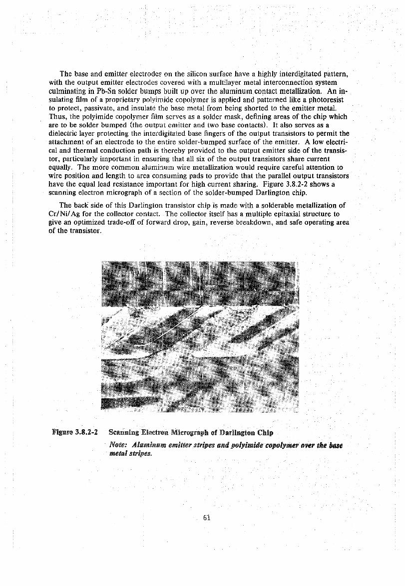
The base and emitter electrodes on the silicon surface have a highly interdigitated pattern, with the output emitter electrodes covered with a multilayer metal interconnection system culminating in Pb-Sn solder bumps built up over the aluminum. contact metallization. An insulating film of a proprietary polyimide copolymer is applied and patterned like a photoresist to protect, passivate, and insulate the base metal from being shorted to the emitter metal. Thus, the polyimide copolymer film serves as a solder mask, defining areas of the chip which are to be solder bumped (the output emitter and two base contacts). It also serves as a dielectric layer protecting the interdigitated base fingers of the output transistors to permit the attachment of an electrode to the entire solder~bumped surface of the emitter. A low electrical and thermal conduction path is thereby provided to the output emitter side of the transistor, particularly important in ensuring that all six of the output transistors share current equally. The more common aluminum wire metallization would require careful attention to wire position and length to area consuming pads to provide that the parallel output transistors have the equal lead resistance important for high current sharing. Figure 3.8.2-2 shows a scanning electron micrograph of a section of the solder-bumped Darlington chip.
The back- side of this Darlington transistor chip is made with a solderable metallization of Cr/Nil Ag for the collector contact. The collector itself has a multiple epitaxial structure to give an optimized trade-off of forward drop, gain, reverse breakdown, and safe operating area of the transistor.
Figure 3.8.2-2 Scanning Eledron Micrograph of Darlington Chip
Note: Aluminum emitter stripes and polyimide copolymer o.,er the kre metal stripes.
61
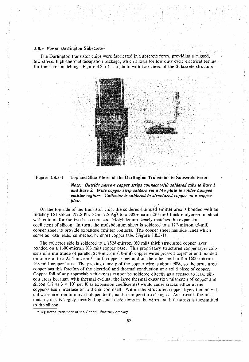
3.8.3 Power Darlington Subscrete®
The Darlington transistor chips were fabricated in Subscrete form, providing a rugged, low-stress, high-thermal dissipation package, which allows for low duty cycle electrical testing for transistor matching. Figure 3.8.3-1 is a photo with two views of the Subscrete structure.
Figure 3.8.3-1 Top and Side Views of the Darlington Transistor in Subscl'ete Form
Note: Outside narrow copper strips connect with soldered tabs to Base 1 and Base 2. Wide copper strip solders via a Mo plate to solder bumped emitter regions. Collector is soldered to structured copper on a copper plate.
On the top side of the transistor chip, the soldered-bumped emitter area is bonded with an Indalloy 151 solder (92.5 Pb, 5 Sn, 2.5 Ag) to a 50S-micron (20 mil) thick molybdenum sheet with cutouts for the two base contacts. Molybdenum closely matches the expansion coefficient of silicon. In turn, the molybdenum sheet is soldered to a 127-micron (5-mil) copper sheet to provide expanded emitter contacts. The copper sheet has side lanes which serve as base leads, connected by short copper tabs (Figure 3.S.3-1).
The collector side is soldered to a 1524-micron (60 mil) thick structured copper layer bonded on a 1600-micron (63 mil) copper base. This proprietary structured copper layer consists of a multitude of parallel 254-micron (10-mil) copper wires pressed together and bonded on one end to a 25.4-micron (I-miI) copper sheet and on the other end to the 1600-micron (63-mil) copper base. The packing density of the copper wire is about 90%, so the structured copper has this fraction of the electrical and thermal conduction of a solid piece of copper. Copper foil of any appreciable thickness cannot be soldered directly as a contact to large silicon areas because, with thermal cycling, the large thermal expansion mismatch of copper and silicon (17 vs 3 x 10⁶ per K as expansion coefficients) would cause cracks either at the copper-silicon interface or in the silicon itself. Within the structured copper layer, the individual wires are free to move independently as the temperature changes. As a result, the mismatch stress is largely absorbed by small distortions in the wires and little stress is transmitted to the silicon.
@ Registered trademark of the General Electric Company
62
With the usage of two propnetary techmques - structured copper, and chip polYlmlde copolymer passlvatlOn and Isolation - and solder bumpmg on the chip With a molybdenum stress rehef plate, the Subscrete package has the followmg deSirable features
• Rugged structure
• Compact and low profile
• Excellent thermal dlsslpatlOn
• All soldered Jomts
• Low stress structure to Withstand thermal cyclIng
• Testable to full current ratmgs at low duty cycle for precise matchmg of gam
3.8.4 Thermal Resistance and Thermal Cycling
The thermal diSSipatIOn of the Subscrete IS a cntIcal conSideratIon for high-power mverter operatIOn, partIcularly because many transistors must be m parallel and near-equal currents are necessary to share the electncal and thermal loads wlthm each module The Subscrete IS soldered to a copper heat spreader, which m turn IS fastened by screws to a heat smk common to all of the Subscretes m a half-phase module An analYSIS has been made of the heat flow under deVice operatIOn from the transistor chip through the structured copper, copper plate, copper heat spreader, and mto the heat smk The results of thiS analYSIS are shown m Table 3 84-1, With the actIve output emItter area of the transistor chip taken as 1.4 cm2
(0.22 m2) or about 60% of the total chip area, and the solder layer represented by Pb
Table 3.8.4-1
THERMAL RESISTANCE (J unction to Sink)
L A a- R(J=L/Aa-Matenal Thickness Area ConductIVity ReSistance
cm cm2 watt/cm K K/watt
SI 0028 1 4 1 2 0017
Pb 00025 14 034 0005
Structured Cu 015 1 4 34 0031
Cu 0.16 1 4 37 0.031
Pb 0.0025 1 6 0.34 0004
Cu heat spreader 048 146 37 0.05-0 12
Thermal grease 0.0025-0 006 146 0007
o 14-020
63

A graph which relates the thermal resistance ~unctIon to SInk) to the area of the copper heat spreader IS given as Figure 3.84-1. For this graph, the thickness of the thermal grease layer was taken as 0.0028 cm, or Just over 1 mIl It IS clear that IncreaSIng the heat spreader beyond the chosen area of 15 cm2 does not Yield any real reductIon In the overall thermal resistance.
T H E R M A L
R E 5 I 5 T A N C E
o E G
C I \I A T T
" 21
" 2
" 19
" 18
" 17
" IS
o 15
" 14
o 13
o 12
- THERMAL GREASE 0 0028CM THICK
" 2 5 5 7 5 1 0 1 2 5 1 5 1 7 5 20 22 5 25 27 5 3"
AREA OF COPPER HEAT SPREADER IN CM2
Figure 3.8.4-1 Thermal Resistance of Darlington Subscrete
The major uncertaInty IS In the calculatIOn of the loss through the heat spreader and thermal grease to the heat SInk (assumed to remaIn at a fixed temperature) The analysIs considered the direct thermal resistance due to heat conductIOn from the bottom of the active chip area through all the layers, In parallel with thiS, a spreadIng resistance, due to heat conductIon, out radially In the heat spreader and then through the poorly conductIng thermal grease (Wakefield EngIneerIng, Inc Type 120 Thermal JOInt Compound) The thickness of thiS grease layer IS difficult to determIne and to reproduce
Thus, expenmental measurements on a large number of Subscretes soldered to heat spreaders and then attached to a heat SInk show some spread In R(} values, as Indicated In Figure 3.8.4-2 These data were derived from measunng the shift In emitter-base voltage (calIbrated agaInst temperature) after heat pulses of about ten seconds were applIed by operatIon of the transistor Presumably, the one very high R(} value represents a case of poor solder attachment With SignIficant area VOids or cracks to greatly Increase the thermal resistance of the solder layers Such a Subscrete was rejected for usage
The relIabilIty of the mounted Subscrete was checked by thermal cyclIng between 223 K (-50°C) and 398 K (125 DC), a half hour at each temperature Through 50 such cycles, no change was measurable In the thermal resistance, a far more sensitive indicator of deVice degradatIOn than the electncal parameters, such as forward voltage drop, gaIn, or reverse breakdown
64

5 I
I
I 4 ~
I
I F
~ q E 3 0 I u
I ;-., C
2 1 y
I 1 I
l I
'" -t----r 0 50 250
IEZJ Y ,~~RMAL ~ESrSTA~CE DEC C/WATT
Figure 3.8.4-2 Experimental Measurements of Subscrete Thermal Resistance
Note: 18 Subscretes mounted with thermal grease on a heat sink. Heat t spreader area is 14.6 cm 2
• Calculated thermal resistance is 0.17 ± 0.03 Klwatt.
3.8.5 Electrical Performance
The reverse breakdown of the ZJ504 Subscretes chosen for module fabncatlOn was at least 450 volts at 0 5 rnA A tYPIcal dc common emItter gam (hFE) dependence on collector current IS plotted m FIgure 3 8 5-1 for three dIfferent temperatures Note the gam reduction at hIgher temperatures for hIgher collector currents The transIstors were matched usmg the collector-emItter voltage VCE for a base current of 2 A and an emItter current of eIther 140 A or 160 A The VCE charactenshc was read from a curve tracer dIsplay under low duty cycle WIth the transIstor mounted on a hot plate held at 398 K (125 DC). ThIS hIgher temperature rather than room temperature was used for matchmg because of the gam falloff WIth temperature and deSIre to match at the more cntlcal Junctlon temperature Values of VCE at 140 A m one batch of 20, for example, vaned from 0 88 volt to 1 20 volts, but three groups of four transIstors could be chosen to match withm 0 04 volt The reverse breakdown V CEO (base open) for an emItter current of 0 5 rnA vaned from 450 to 700 volts
65

CURRENT GAIN HFE OF DARLINGTON TRANSISTORS AT THREE TEMPERATURES, VCE=2 0V. PAI8-20-2 TRANSISTOR
1400
- 25 DEG C (.;J91 K)
C 1200 6'---.., ---- 75 DEG C (3'(1 K..) " -, --- 125 DEG C (3'11 ~) U I "'\
R I ,
R 1000 / \
E , \ N I . .......... - ............ - \ T
, '- '
" 800
, I '\', G
I ' ' A \",
I / " ",
600 , , N I ,
H F 400 E ,
"- , , 200
0
0 25 50 75 100 125 150 175 200 225 250
COLLECTOR CURRENT IN AMPERES
Figure 3.8.5-1 Gain Characteristic of ZJ 504 Darlington Transistor
3.8.6 Power Module
The maXImum current through one power module of the three-phase mverter CIrcUIt IS 600 A. WhIle mdlvldually mounted ZJ504 transIstors could be operated at well over 200 A and three transIstors could, m pnnclple, supply 600 A, It was desIrable to parallel four tranSIStors to provIde some safety margm for current shanng among the transIstors Furthermore, wIth four transIstors there was better thermal dIssIpatIon to hmlt the JunctIon temperature under the most demandmg condItIOns of power delIvery.
Four matched Subscretes soldered to copper heat spreaders of dImenSIOns 3.175 cm x 4.763 cm (1.25-mch x 1 875-inch) were mounted on a common nIckel-plated heat smk to form the transistor portIon of a power module. The mdlvidual Subscretes were bolted down to the heat smk wIth thermal grease under each Subscrete to Improve the heat flow FIg-ure 3 8.6-1 IS a photo of the power module, wIth the Darhngton ChIP and Subscrete in the foreground, whIle FIgure 3.8 6-2 shows the open power module In additIon to the four DarlIngton transIstor Subscretes, the module also has two dIOdes m parallel m an antI-parallel configuratIOn to the four parallel transIstors These dIodes are fast recovery diodes which alIowa path for reactIve and regeneratIve currents, whIle preventmg reverse current and voltage of the transistors and the resultmg mverted mode operatIOn. The diodes used in these power modules were InternatIOnal RectIfier type 251 UL dIodes wIth 02 mIcrosecond turnoff, obtained m chip form wIth a molybdenum backmg plate. These dIodes were mounted on
66
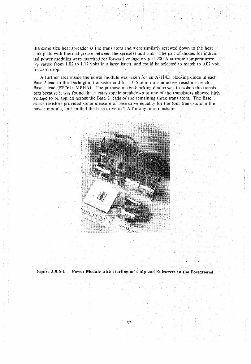
the same size heat spreader as the transistors and were similarly screwed down to the heat sink plate with thermal grease between the spreader and sink. The pair of diodes for individual power modules were matched for forward voltage drop at 200 A at room temperatures; VF varied from 1.02 to 1.12 volts in a large batch, and could be selected to match to 0.02 volt forward drop.
A further area inside the power module was taken for an A-114D blocking diode in each Base 2 lead to the Darlington transistor and for a 0.5 ohm non-inductive resistor in each Base 1 lead (EP7644 MPHA). The purpose of the blocking diodes was to isolate the transistors because it was found that a catastrophic breakdown in one of the transistors allowed high voltage to be applied across the Base 2 leads of the remaining three transistors. The Base 1 series resistors provided some measure of base drive equality for the four transistors in the power module, and limited the base drive to 2 A for anyone transistor.
Figure 3.8.6-1 Power Module with Darlington Chip and Subscrete in the Foreground
67
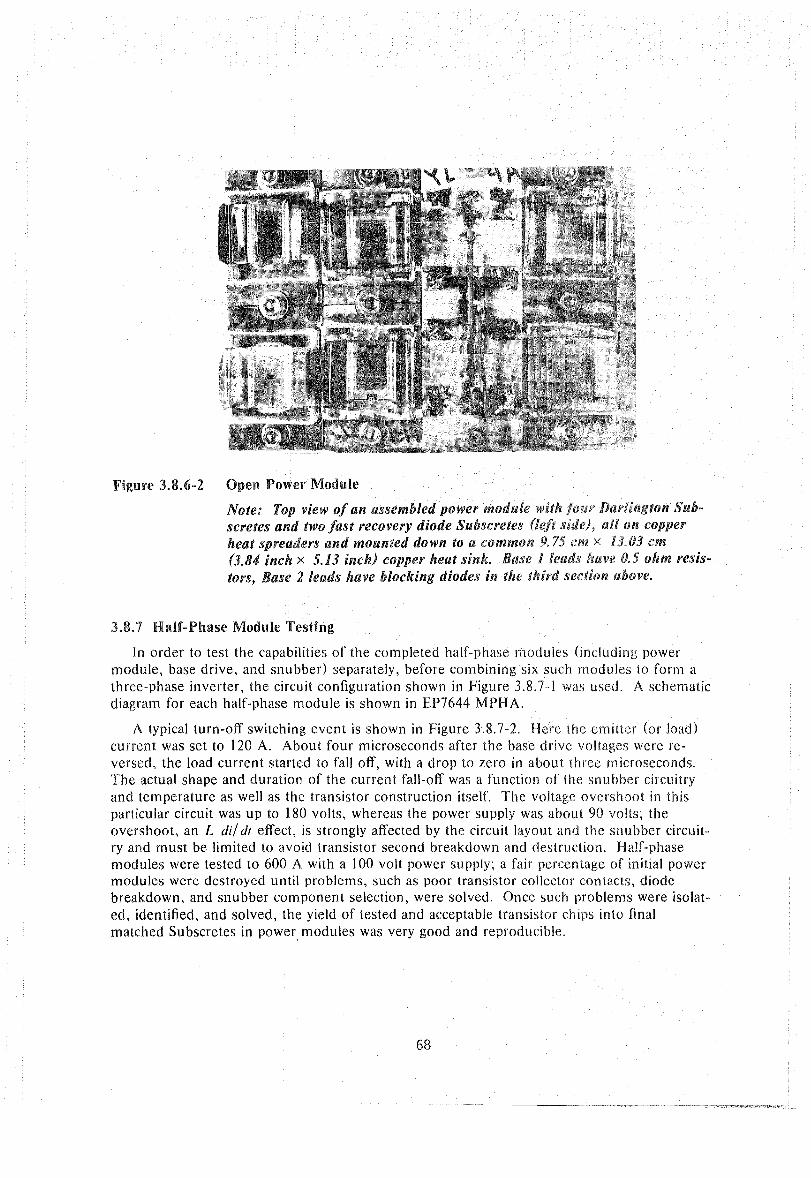
Figure 3.8.6-2 Open Power Module
Note: Top view of an assembled power module with scretes and two fast recovery diode Subscretes (left on copper heat spreaders and mounted down to a commoll 9.75 em x 13.03 em (3.84 inch x 5.13 illch) copper heat sillk. Base 1 leads 0.5 ohm resis-tors, Base 2 leads have blockillg diodes in the section above.
3.8.7 Half-Phase Module Testing
In order to test the capabilities of the completed half-phase modules (including power module, base drive, and snubber) separately, before combining six such modules to form a three-phase inverter, the circuit configuration shown in Figure 3.8.7-1 was used. A schematic diagram for each half-phase module is shown in EP7644 MPHA.
A typical turn-off switching event is shown in Figure 3.8.7-2. Here the emitter (or load) current was set to 120 A. About four microseconds after the base drive voltages were reversed, the load current started to fall off, with a drop to zero in about three microseconds. The actual shape and duration of the current fall-off was a function of the snubber circuitry and temperature as well as the transistor construction itself. The voltage overshoot in this particular circuit was up to 180 volts, whereas the power supply was about 90 volts; the overshoot, an L di/ df effect, is strongly affected by the circuit layout and the snubber circuitry and must be limited to avoid transistor second breakdown and destruction. Half-phase modules were tested to 600 A with a 100 volt power supply; a fair percentage of initial power modules were destroyed until problems, such as poor transistor collector contacts, diode breakdown, and snubber component selection, were solved. Once such problems were isolated, identified, and solved, the yield of tested and acceptable transistor chips into final matched Subscretes in power modules was very good and reproducible.
68
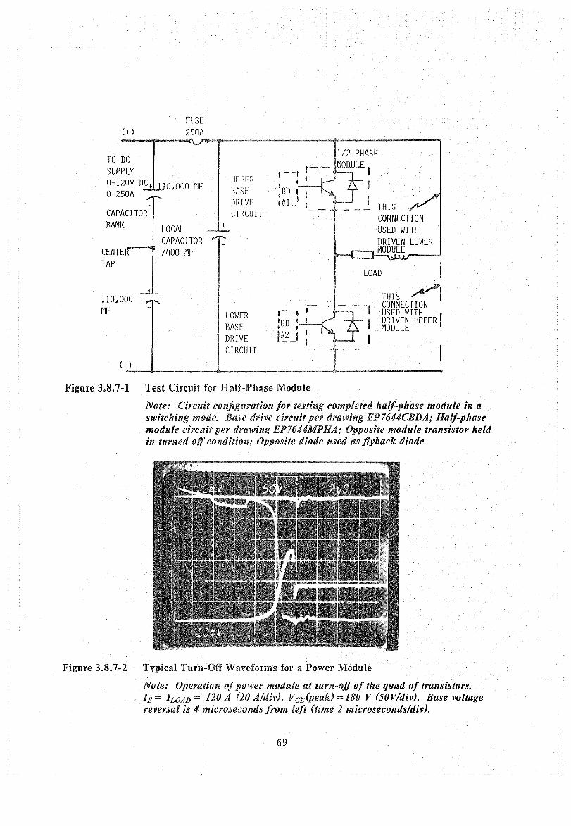
FUSE (+) 250A
-~'~
TO DC 112 PHASE
SUPPLY 1- -, OillJL£.,
O-120V DC,_ lJPfJFH I - I OJ 000 [1F B/\SI 'rm I 0-250/\ , I I DRIVF I/D_ D THIS CI f{CUlT CONNECTION
BANK + USED WITH CAPACITOR
TAP LOAD
110,000 THIS ~I flF - --I CONNECTION
LOWER '--I USED WITH BASE IBD I I I DRIVEN UPPER I
i I MODULE DRIVE I~-' I CIRCUIT
(-) ----~--.------~.--------------
Figure 3.8.7-1 Test Circuit for Half-Phase Module
Note: Circuit configuration for testing completed half-phase module in a switching mode. Base drive circuit per drawing EP7644CBDA; Half-phase module circuit per drawing EP7644MPHA; Opposite module transistor held in turned off condition; Opposite diode used as flyhack diode.
F'igure 3.8.7-2 Typical Turn-Off Waveforms for a Power Module
Note: Operation of power module at turn··off of the quad of transistors. h = hOAD = 120 A (20 A/div), VCE(peak) =180 V (50V/div). Base voltage reversal is 4 microseconds from left (time 2 microseconds/div).
69
3.9 CONTROLLER FAMILY EXPANSION
A specific objective of the contract was to develop preliminary designs and design gUldehnes to expand the eXisting 20 hp 108-volt controller to cover a wide range of motor horsepower ratings and battery system voltages The motor horsepower range specified IS for vehicles requmng a 10, 20, 30, 40, or 50 hp motor. The battery system voltage range for each of the motors IS from 96 ± 12 volts to 270 ± 30 volts Specific nominal battery system voltage values of 84 volts, 108 volts, 150 volts, and 300 volts have been chosen for evaluatIOn The larger motors are Intended to be applicable to heavier passenger vehicles, delivery vans, and trucks for urban service In accordance with the J227a - Schedule D dnvIng cycle
3.9.1 Assumptions
In order to make such a senes of deSigns, numerous assumptions are necessary to define the framework for the system deSigns The major assumptIOns are outhned below
1) All system deSigns are based on the eXisting laboratory deSign 20 hp, 108-volt battery system No attempt has been made to cost-reduce thIS baSIC deSign as would be deSirable before committing to a prototype production deSIgn
2) All system deSigns are based on power and/or voltage ratios from the eXisting deSign, I e., a scaling approach IS used
3) No attempt was made to ensure that the vehicles USing different dnve motors would meet any specIfic duty or dnvIng cycle
4) The "Tractive Effort vs Speed" curve for all dnves maintained the same speeds for tranSItIOn of operating modes of the Inverter.
5) All system partitIOning IS based on state-of-the-art technology, although some product deSign work may be necessary to achIeve requested component ratings
Examination of the controller for the range of motor horsepower and battery system voltage levels reveals that the system can be diVided Into two major portions' the power CirCUit, and the senSing and control CIrCUIts The power CIrCUIt components WIll vary for each and every power and voltage level. In contrast, the control CirCUIt Will remain fixed and one set of CirCUIt components can be used for any system The controller family deSigns reflect thIS dIVISIOn of the system
3.9.2 Input Capacitor Scaling
3.9.2.1 Summary
Because the mput capaCItor bank IS a large part of the controller In volume and cost, It IS always called upon to do more than the technology allows As of thiS study, the availability of hIgh-voltage capaCItors required for apphcatIOn m the 300-volt system does not eXist An extrapolatIOn of those capacitors used In the low-voltage systems WIll be made
Table 3 92 1-1 gives the reqUired ratings of the capaCItor bank The total capaCitance, voltage rating, and total npple current reqUIred are scaled from the base values Ta-ble 3 92 1-2 hsts hand chosen values of capaCItance which satisfy or exceed the minImUm capacitance and npple current ratings reqUIred for the system The values do not represent commerCially avaIlable values, but are interpolatIOns based on commerCially aVailable capaCItors offered, from stock, by Cornell-Dublher Electnc CorporatIOn. (13) Also listed IS the interpolated capaCItor volume Because the capacitor technology IS changing and custom packaging has not been conSidered, the volume estimates of Table 3 9 2 1-2 can vary 10-20%
70

J;',H. V 10 Hf
c= (IJF' 3.tc.9t> S4V I r-IFFl ~ 8R.C'o~/1
V ru!tT It.,; 15:'1.5~6
c= \ U,-) :::200 103V I F.IfFLE 66.C'l4
V F.ATING 200
c= (UF) 11508.:-150V I F.IFFLE" 49.63,··8
'J F.ATING :77.778
r= (UF) 2877.1:' 3(01) I F.IF Fl f :?4.d184
V F.ATIrW 5~5.~~o
Bat V
C = (UF) 84V I RIPPLE
V RATED VOL (IN)
C = (UF) 108V I RIPPLE
V RATED VOL (IN)
C = (UF) 150V I RIPPLE
V RATED VOL (IN)
C = (UF) 300V I RIPPLE
V RATED VOL (IN)
Table 3.9.2.1-1
REQUIRED CAPACITOR RATINGS
.... () Hf 3l) H' 40 HF
73J~L,.Q 11 P-)"'4 14 • ., 7Q'2 177 ..... 74 26~j ...... 11 3~4.:-;4q
1 ~~" ~::;CI 1~5.~~,t. 155.~5o
4440v 61")':""'\' b22;0 137.':<3 20~.82 271).7.:-. 200 200 200
23017 345'"'5.4 4,,011.5' 9l.2736 14,1.01 19a.~J..:t7
277.7-'8 277.r2 277 ..... 78
5754.24 8,.,31.36 1150~.5
49.D3bc. 74.4~~:: ~5'.2736
~5~j. :)~6 55~. 5~Jo 5~5.~56
Table 3.9.2.1-2
CAP ACITOR SELECTIONS
10 HP 20HP 30HP 40HP 50HP
367E3 734E3 113E3 160E3 210E3 106 186 266 354 443 156 156 156 156 156 182 352 530 737 953
222E3 450E3 742E3 105E3 138E3 768 139 207 276 345
200 200 200 200 200 175 338 537 741 955
11.5E3 249E3 409E3 582E3 764E3 525 992 149 198 248
278 278 278 278 278 125 251 392 538 688
29E3 58E3 86E3 116E3 144E3 251 496 74.5 994 124.2
556 556 556 556 556 125 222 308 394 472
71
51' HF
18 l7 .)
41 • ! 8 .... 1 ~, • 5~.·)
111000 34 ... \ t; 200
5751'").4 248.124 ~77 • 77,~
14.!f:5.0 1 -;4 t 0'7 ! c: r r" c: c::- I-....... .1 .. '. ,-'~'"

The base values for the 20 hp, 108 volt system are
C = 44400 J.LF
V= 200 V
I = 138 A (RMS RIpple)
3.9.2.2 Assumptions
1 There IS no change In frequency or npple current wave shape characteristIc to effect capacItance ratIng
2 The Input capacItor supphes amounts of energy whIch are proportIOnal to the system energy for any horsepower ratIng
3.9.2.3 Calculations
For constant supply voltage and varYIng horsepower, the energy stored by the capacItor bank vanes proportIOnally SInce voltage remams fixed, the capacItance varies proportIOnally Thus,
Where,
C = (HP/HP b) Cb
I = (HP/HP b) Ib (RIpple current)
C = deSIred capacItance value
Cb = base value of capacItance for 20 hp, 108 V system (44400 J.LF)
HP = desIred horsepower ratIng
HP b = base value of horsepower (20 hp)
I = deSIred ripple current ratIng
Ib = base value of npple current (138 A, RMS)
MaIntaInIng horsepower constant and varYIng supply voltage will vary the capacitance value as the Inverse square RIpple current WIll vary as the Inverse. Thus,
C = (Eb/ E)2 Cb
V = (E/ Eb) Vb
I = (Ei E) Ib (RMS npple)
Where, E = deSIred supply voltage
Eb - base value of supply (108 v)
V = deSIred capacItor module voltage ratIng
Vb base value of voltage rating (200 V)
The Interpolated capacitor bank volume for the 156-volt rated capacItor is calculated by:(3)
72
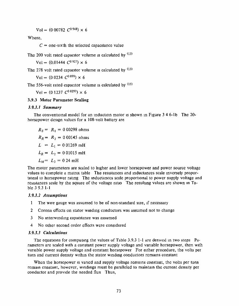
Vol = (0 00782 CO 948) X 6
Where,
C = one-sIxth the selected capaCItance value
The 200 volt rated capaCItor volume IS calculated by (13)
Vol = (0.01444 CO 927) X 6
The 278 volt rated capacitor volume IS calculated by (13)
Vol = (00234 CO 899) X 6
The 556-volt rated capacitor volume IS calculated by (13)
Vol = (0 1237 CO 8293) X 6
3.9.3 Motor Parameter Scaling
3.9.3.1 Summary
The conventlOnal model for an mductton motor IS shown m Figure 34 6-1b The 20-horsepower deSIgn values for a 108-volt battery are
Rs = RI = 000298 ohms
RR = R2 = 000145 ohms
L = LI = 001269 mH
LR = L2 = 001015 mH
LM = L3 = 0 24 mH
The motor parameters are scaled to hIgher and lower horsepower and power source voltage values to complete a matnx table The resistances and mductances scale mversely proportIOnal to horsepower ratmg The mductances scale proportIOnal to power supply voltage and reSIstances scale by the square of the voltage ratIO The resultmg values are shown m Table 3 9.3 1-1
3.9.3.2 Assumptions
1 The WIre gauge was assumed to be of non-standard SIze, If necessary
2 Corona effects on stator wmdmg conductors was assumed not to change
3 No mterwmdmg capaCItance was assumed
4 No other second order effects were conSidered
3.9.3.3 Calculations
The equations for computmg the values of Table 3.9.3 1-1 are denved 10 two steps Parameters are scaled WIth a constant power supply voltage and vanable horsepower, then WIth vanable power supply voltage and constant horsepower For either procedure, the volts per turn and current denSity wlthm the stator wmdmg conductors remams constant
When the horsepower IS vaned and supply voltage remams constant, the volts per turn remam constant, however, wmdmgs must be paralleled to maintam the current denSIty per conductor and proVide the needed flux Thus,
73
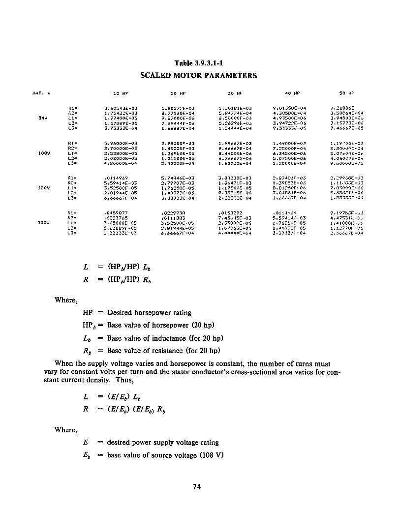
il~T. v
R1= r..2=
84V Ll= L2= L3=
Rl= R2=
108V L1= L2= L3=
Rl= R2=
150V Ll= L2= L3=
Rl= R2=
300V Ll= L:= L3=
Where,
Table 3.9.3.1-1
SCALED MOTOR PARAMETERS
10 HP
3.60543E-03 1.75432E-03 1.97400E-05 1.57889E-05 3.73333E-04
5.96000E-03 2.90000E-03 2.53800E-05 2.03000£-05 4.80000E-04
.0114969 5.59414E-:>3 3.5:!500f-05 2.81944E-05 6.66667F-04
.0459877
.0223765 7.05000E-05 5.63889F-OS 1.33333E-v3
L - (HP JHP) Lb
R - (HP b/HP) Rb
20 HP
1.8027:'<-03 8.77160[-04 9.87()00E-06 7.89444F-06 1.861>67E-·)4
2.98000""-03 1.45000F-03 1.26900E-05 1.01500£-05 2.40000F-04
5.74R46E-03 2.79707E-03 1.76:!SOE-05 1.4097:'E"-0:; 3.33333E-04
.0229938
.0111883 3.5:!500E-O!j :!. 81 Q441E-O~ 6.66667F-C)4
HP = Desired horsepower rating
30 HF
1.20181E-03 5. 84774E-'')4 6.58000F-06 5.26296E.-Ob 1.24444E-04
1.98667E-03 9.66667£-04 8.460001:.-06 6.76667£:-06 1.60000E-04
3.8J230E-03 1.86471F-03 1.17500E-05 9.39915E-06 2.222~:!E-04
.Ol!"i3:?9:2 7.4:itH5E"-03 2.3';000E-0'j 1.bI963E-0'j 4.44444E-04
HP b = Base value of horsepower (20 hp)
Lb - Base value of inductance (for 20 hp)
Rb - Base value of resistance (for 20 hp)
40 HP 50 HP
9.01353E-04 7.21086E 4.385801:.-C4 3.50E:64E-04 4.9J500E-06 3.94800E-0" 3.94722E-O!> 3.1~773L-06
9.3,333<" -0'5 7.46667E-05
1.49000E-03 1.19'00l-03 7.2~000F-04 5.80()0<'C-04 6.34500E-06 5.07«0')E-O" 5.07500E-06 4.060C<'E-0., 1.20000E-04 9. oO()(\'')E-\'~,
2.874~3F-03 2.29938E-03 1.39853E-03 1.11<':33E-03 8.81250E-06 7.0':1000[-06 7.048611':-0 ... ~.638r9F-06
1.66667F-,)4 1.33133E-04
.0114"6'" 9.197~.3F-lJJ 5.59414,:-03 4.475311-.-0., 1.76250E-05 1.41000E-O~. 1 • 40"l72f -O~ 1. 12778t -05 3. 33J3.<~ -04 2./",,,!>67E"-04
When the supply voltage varies and horsepower is constant, the number of turns must vary for constant volts per turn and the stator conductor's cross-sectional area varies for constant current density. Thus,
L - (E/ Eb) Lb
R - (E/ Eb) (E/ Eb) Rb
Where,
E - desired power supply voltage rating
Eb - base value of source voltage (l08 V)
74
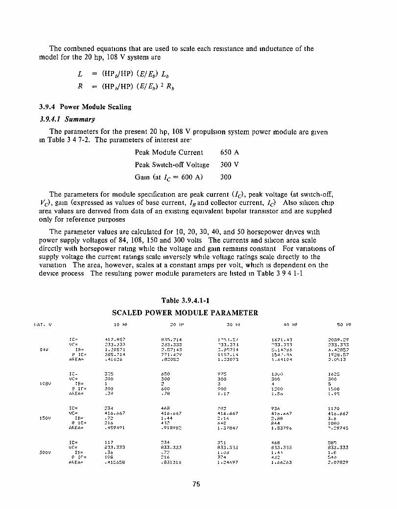
The combmed equatIOns that are used to scale each resistance and mductance of the model for the 20 hp, 108 V system are
L = (HP b/HP) (E/ Eb) Lb
R - (HP JHP) (E/ Eb) 2 Rb
3.9.4 Power Module Scaling
3.9.4.1 Summary
The parameters for the present 20 hp, 108 V propulsIOn system power module are given m Table 347-2. The parameters of interest are'
Peak Module Current
Peak SWitch-off Voltage
Gam (at Ie = 600 A)
650 A
300 V
300
The parameters for module specificatIOn are peak current (Ie), peak voltage (at sWitch-off, Ve), gam (expressed as values of base current, In and collector current, Ie) Also slhcon chip area values are denved from data of an eXlstmg eqUIvalent bipolar transistor and are supphed only for reference purposes
The parameter values are calculated for 10, 20, 30, 40, and 50 horsepower dnves with power supply voltages of 84, 108, 150 and 300 volts The currents and SIlIcon area scale directly with horsepower ratmg while the voltage and gam remams constant For vanatIOns of supply voltage the current ratmgs scale mversely whIle voltage ratings scale directly to the vanatlon The area, however, scales at a constant amps per volt, which IS dependent on the deVice process The resultmg power module parameters are hsted m Table 394 1-1
Table 3.9.4.1-1
SCALED POWER MODULE PARAMETER
l.AT. V 10 Hf- :CO Hf- 30 Hf 40 HF 50 HF
IC= 417.857 835.714 1 -'C:J ~ t 51 1671.43 :!039.:C9 Vf= :!33.333 :!.33.333 '33.33~ '"'33.331 :?33.313
84V IF<= 1.28571 2.~7143 :.8c;714 ~j.142c:~6 6.4"2857 (J IC= 385.714 771.4:C." 1157.14 154~.86 1928.57
AF.EA= .410:?6 .82052 1.:C307'3 1.64104 2.0(.J13
IC- 3~5 650 97:; l.3v') 16~~
VC= 300 300 300 300 300 108V IE<= 1 :c 3 4 5
@ If= 300 600 900 1:C00 l~JOO AF.EA= .39 .78 1.17 1. :'0. 1.9<,
IC= :!34 41'>8 70:! 936 1170 VC= 416.1'>67 416.667 416.667 416.067 416.667
150V IE<= .72 1.44 :Col6 :!.88 3.6 @ IC= ::?16 41::! 648 81.4 1080
AF.EA= .459491 .9189S:C 1.37847 1.83796 "'.29745
IC= 117 ::!34 3 Cjl 468 58') VC= a33.333 833.333 833.31.3 813.333 833.333
300V IE<= .36 .72 l.va 1.41 1.8 (J Ir= 108 ::16 ::1:'4 4.3:! ~4v
Af,EA= .41~658 .831316 1.:C41>97 1.66:C63 :?078:C9
75

3.9.4.2 Assumptions
1 Changes 10 peak sWitch-off voltage are due solely to vanatIons of power supply voltage rat10g No effect from changes of 10ductance of 1Oterconnect leads IS assumed
2 Silicon area calculatIOns use two bipolar transistor types, one under development, the other commerCially available, as bases for calculation
3 The sWltch10g speed of the module remams constant for any rat10g
4 Thermal specificatIOns remam the same
5 The charactenstIc shape of the tractive effort versus speed curves remams the same and the corner speed does not change
3.9.4.3 Calculations
The equatIOns for comput1Og the values of Table 394 1-1 were denved 10 two steps Parameters were scaled With constant supply voltage and vanable horsepower then With vanable supply and constant horsepower For either procedure the parameter values are dependent on the system vanatlOn, not the device
For constant supply voltage and vanable horsepower, the current for the system and hence, for the module scales proportIOnally Thus,
Ic = (HP/HP b) ICb
IB - (HP/HP b) IBb
Where,
Ic = Module current at desired horsepower
IB - Gate current (transistor base current) at the desired horsepower
ICb = Base value of module current (650 A)
IBb = Base value of gate current (2 A, Ic = 600 A)
For constant horsepower and vanable supply voltage the current for the system vanes 10-versely as the supply voltage Thus,
Ic = (Eb/ E) ICb
IB = (EJ E) IBb
Vc (E/ Eb) VCb
Where,
E = desired supply voltage rat10g
Eb - base value of supply (l08 V)
Vc - desIred peak sWitch-off voltage
VCb = base value of sWitch-off voltage (300 V)
The sIhcon AREA contamed in the module is a direct measure of the cost. For constant supply voltage the silicon area 10creases proportIonally as the horsepower to maintain a constant current density ThiS IS conceptually equal to parallelIng the internal transistor chips Thus,
76
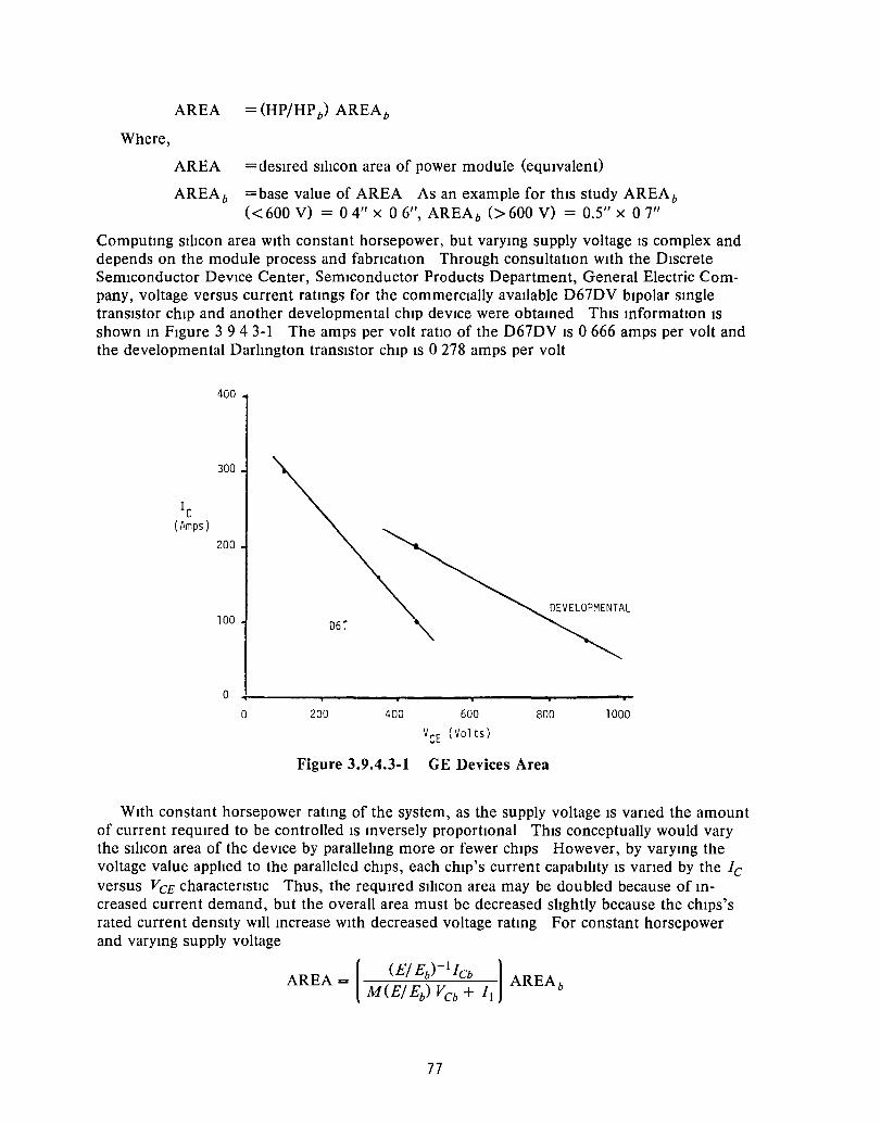
Where,
AREA =desired sIhcon area of power module (equIvalent)
AREAb =base value of AREA As an example for thIS study AREAb « 600 V) = 0 4" x 0 6", AREAb (> 600 V) = 0.5" x 0 7"
Computmg sIhcon area wIth constant horsepower, but varymg supply voltage IS complex and depends on the module process and fabncatlOn Through consultatlOn wIth the DIscrete Sem1conductor DeViCe Center, Sem1conductor Products Department, General Electric Company, voltage versus current ratmgs for the commercially avaIlable D67DV bIpolar smgle tranSIstor ch1p and another developmental ChIP deVIce were obtamed ThIS mformatIOn IS shown m F1gure 3 9 4 3-1 The amps per volt ratto of the D67DV IS 0 666 amps per volt and the developmental Darhngton tranSIstor chIP IS 0 278 amps per volt
Ie (Amps)
400
300
200
100
o o 200 400 600 800 1000
VeE (Volts)
Figure 3.9.4.3-1 GE Devices Area
WIth constant horsepower ratmg of the system, as the supply voltage IS vaned the amount of current reqUlred to be controlled 1S mversely proportIOnal ThIS conceptually would vary the sIhcon area of the deVIce by parallehng more or fewer ChIPS However, by varymg the voltage value apphed to the paralleled ChIPS, each ch1p's current capabIhty 1S vaned by the Ie versus VeE charactensttc Thus, the reqUlred s1hcon area may be doubled because of mcreased current demand, but the overall area must be decreased shghtly because the ch1ps's rated current denSIty WIll mcrease WIth decreased voltage ratmg For constant horsepower and varymg supply voltage
AREA = I (Ej Eb)-I Ieb I AREAb M(Ej Eb) VCb + II
77
Where,
M = amps per volt ratIo of the current vs voltage ratIng characterIstIcs for the ChIP devIce beIng consIdered
II = The artIficIal current value of the characterIstIc ratIng curve for a supposed zero voltage applIed (vertIcal aXIS Intercept of the curve)
The fundamental derIvation of the current versus voltage ratIngs curve maIntaInS a constant devIce gaIn when operated wIthIn the ratIngs
The final area equatIon for varYIng horsepower ratIng and voltage IS'
AREA = (HPjHP b) I (Ej Eb)-l ICb I AREAb M(Ej Eb) VCb + II
3.9.5 Power Module Snubber Scaling
3.9.5.1 Summary
The actual values for the resIstive and capacItive components, scaled for different horsepowers and supply voltages, are not presented due to the complexIty of the CircUIt and dependence on waveshape characterIstics However, the equations for calculatIng the ThevenIn equIvalent resIstance and capaCItance are gIven
3.9.5.2 Assumptions
1 The amount of overshoot voltage seen across the power module IS dIrectly proportIOnal to the supply voltage and IS unaffected by current, to a first order approximatIon
2 Interconnect Inductances remaIn constant
3. The characterIstic waveshape of the energy whIch the snubber IS absorbIng changes only In magmtude, not time (The tIme Interval of snubber operatIon remaInS constant.)
4 The pOSSIble resonance of the motor WIndIng inductance and capaCItance IS a second order effect not needIng conSIderation.
3.9.5.3 Calculations
The equations for scalIng the snubber are denved from the conceptual realIzatIOn of ThevenIn resIstances and capaCItances The CIrCUIt In FIgure 3 9 5 3-1 shows the contrIbutIng components
For constant supply voltage and varIable horsepower, the overshoot voltage must be maIntaIned constant by the snubber. ThIS ensures the power module voltage ratIng remaInS constant At the first Instant of time of snubber operation, the overshoot voltage IS applied dIrectly across the eqUIvalent snubber resIstance and ItS magmtude IS determIned by the current and thIS resIstance Thus, the peak voltage IS'
v = IRs
Where,
V - Peak overshoot voltage
I = Peak motor current occurrIng wIth Vp
Rs EquIvalent snubber resIstance
78

I :>
2:m:F{-tJ w L
CfMF V
MOTOR
~
> V'v Rs
> SNUBBER
Cs
Figure 3.9.5.3-1 Snubber Equivalent Circuit
1 T
Smce the peak voltage must remam constant and the current varies directly as horsepower, the resIstance vanes mversely WIth horsepower Thus,
Where,
I (HP/HP b) h V = (HP/HP b) Ib (HP JHP) Rsb
Rs = (HP b/HP ) Rsb
HP = DesIred horsepower ratmg
HP b = Base value of horsepower
Rsb = EqUIvalent Thevenm resistance at 20 hp rating
Because It IS assumed that the response hme of the snubber network and characterishc wave shape remams constant for any horsepower ratmg, the equivalent snubber capacitor scales dIrectly wIth horsepower Thus,
t - RsCs = (HPb/HP) RsbCs
Cs = (HP/HP b) Csb
Where,
t = Response hme
Cs = Equivalent Thevenm capacitance desIred
Csb = Base value of equivalent capacItance at 20 hp rating
The power of the snubber scales proporhonally with horsepower because the peak overshoot voltage remams constant, the charactenstic waveshape remams constant and the current scales dIrectly wIth horsepower Thus,
P = I V = (HP/HP b) Ib V
P = (HP/HP b) Pb
Where,
P - Snubber dIssIpahon at desired ratmg
Pb - Base value of power diSSIpation at the 20 hp rating
79
.- ,
For constant horsepower and varYing supply voltage, the overshoot voltage vanes directly as supply voltage and the current vanes Inversely This can be seen, again, by the ThevenIn approach The current from the motor (and power sWitches) vanes Inversely as the supply voltage to maintain constant system (P = Pb) Thus,
I = (Eb/ E) Ib
Where,
E = desired supply voltage
Eb = base value of supply voltage (l08 V)
Because the overshoot energy IS due pnmanly to motor Inductance as a generating source, the overshoot voltage vanes directly as supply voltage Thus,
v = L (dIldO
L = (E/ Eb)2 L d [(Eb/ E) 11/ dt
V (E/ Eb) Vb
Where,
L = motor Inductance
t = constant time Interval
USing the above informatIOn and basing the calculatIOns on the same assumptions and time penods as our prevIous calculations, the eqUivalent snubber resistance can be computed as
V = IRs
(E/ Eb) Vb = (EJ E) Ib Rs
Vb = Ib (Eb/ E)2 Rs
Therefore,
Rs = (E/ Eb)2 Rsb
As assumed before, the time response of the network remains constant The eqUivalent capacitance IS
t - Rs Cs
Cs = (EJ E)2 Csb
In summary, the equatIOns which express power consumption and the variation of the eqUivalent ThevenIn resistances and capacitances of the snubber network are
Rs = (HP b/HP) (E/ Eb)2 Rsb
Cs - (HP/HP b) (Eb E )2 Csb
P - (HP/HP b ) Pb
3.9.6 Base Drive Scaling
3.9.6.1 Summary
The approach taken IS to determine the charactenstIcs of the present circuit (reference drawing EP7644CBDA In AppendiX D) and scale them accordingly For reasons of simplicity,
80

It would be highly desirable to mamtam a common circuit and adjust components and coolIng to cover the range This IS done and recommendatIOns for the two mam drIve transistors are summarIzed m Table 396.1-1 The other base drIve circuit components remam basically the same
Table 3.9.6.1-1
BASE DRIVE TRANSISTORS
Motor Horsepower Nommal
Battery Voltage Transistor 10 20 30
Q4 2N5991 2N6338 2N6338 84 Q7 D45H11 D45H11 2N6285
108 Q4 2N5991 2N5991 2N6338 Q7 D45Hll D45H11 D45Hll
150 Q4 D42C5 2N5991 2N5991 Q7 D43C5 D45Hll D45H11
300 Q4 D42C5 D42C5 2N5991 Q7 D43C5 D43C5 D45H11
3.9.6.2 Calculations
The pertment 20 hp lO8-volt power module specificatIOns are
DC Voltage Peak Current Peak SWitch-off Volts Gam at Ie = 600 A
150 V (Brakmg) 650 A 300 V 300
40
MJI0020 2N6285
2N6338 2N6285
2N6338 2N6285
2N5991 D45H11
50
MJI0020 2N6285
MJI0020 2N6285
2N6338 2N6285
2N5991 D45Hll
The gam of 300 IS tYPical at room temperature The base drIve must supply more current than thIS gam would mdicate to account for mmlmum gam transIstors, temperature VarIatIOns, and sharIng among the indIvIdual paralleled DarlIngton transIstors m the power module The present base dnve circUit supplIes 4 amps of posItIve current from Q4 and smks 5 amps of negatIve current wIth Q7
The desIgn value of peak motor current for the 20 hp 108-volt system IS 650 amps ThIS current scales mversely wIth battery voltage and directly with horsepower The peak motor currents are shown m Table 3962-1
The reqUired base dnve currents, both positive and negatIve, are scaled from the peak motor currents, assummg constant gam for the power module The matrIX of base dnve currents are shown m Table 3 9.6 2-2
The matrIX of base dnve currents can be supplIed by selectmg the proper base drIve circuit output transistors. The other portIOns of the base drIve circuit can remam basically the same The number of different output transistors IS lImited to only a few, If Similar base drIve currents are lumped together ThiS IS shown by separatmg the base drIve current matnx m Table 3 9.6 2-2 mto three areas
81
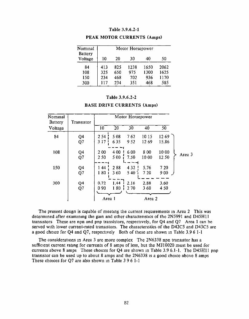
Table 3.9.6.2-1
PEAK MOTOR CURRENTS (Amps)
Nommal Motor Horsepower Battery Voltage 10 20 30 40 50
84 413 825 1238 1650 2062 108 325 650 975 1300 1625 150 234 468 702 936 1170 300 117 234 351 468 585
Table 3.9.6.2-2
BASE DRIVE CURRENTS (Amps)
Nommal Motor Horsepower Battery TransIstor Voltage 10 20 30 40 50
I
84 Q4 254 I , 508 762 10 15 1269 Q7 3 17 I , 635 952 1269 15.86
--- -, 108 Q4 200 400 , 600 800 10 00
I Q7 250 500 I 7.50 10 00 1250
Area 3
----1 L_--t
150 Q4 144 I 288 432 I 5.76 720 I 540 .: Q7 1 80 I 360 720 900
I L ______
300 Q4 ---.,
2.16 2.88 3.60 0.72 1.44 I
Q7 090 1 80 I 270 360 450 '--v---' \. v
J
Area 1 Area 2
The present desIgn is capable of meetmg the current reqUIrements m Area 2 This was determmed after exammmg the gam and other charactenstIcs of the 2N5991 and D45Hli transIstors These are npn and pnp transistors, respectIvely, for Q4 and Q7 Area 1 can be served wIth lower current-rated transIstors. The charactenstics of the D42C5 and D43C5 are a good chOIce for Q4 and Q7, respectIvely Both of these are shown m Table 3.96 1-1
The consideratIons m Area 3 are more complex The 2N6338 npn transIstor has a sufficIent current ratmg for currents of 8 amps of less, but the MJl0020 must be used for currents above 8 amps These chOIces for Q4 are shown In Table 3.96.1-1. The D45H11 pnp transIstor can be used up to about 8 amps and the 2N6338 IS a good choIce above 8 amps These chOIces for Q7 are also shown In Table 396 1-1
82
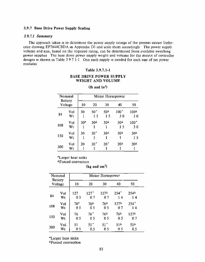
3.9.7 Base Drive Power Supply Scaling
3.9.7.1 Summary
The approach taken IS to determIne the power supply ratIngs of the present CircUit (reference drawIng EP7644CBDA In Appendix D) and scale them accordIngly The power supply volume and Size, based on the reqUired ratIng, can be determIned from available sWitchIng power supplies The base drIve power supply weight and volume for the matrIX of controller designs IS shown In Table 397 I-lOne such supply IS needed for each one of SIX power modules
Table 3.9.7.1-1
BASE DRIVE POWER SUPPLY WEIGHT AND VOLUME
(Ib and in3)
NomInal Motor Horsepower Battery Voltage 10 20 30 40
84 Vol 50 50' 50~ 100' Wt 1 1 5 1 5 30
Vol 30* 30~ 30~ 50~ 108 Wt 1 1 1 1 5
150 Vol 30 30' 30~ 30~
Wt 1 1 1 1
Vol 20 20' 20' 20~ 300 Wt 1 1 1 1
*Larger heat smks ~Forced convectIOn
NomInal Battery Voltage 10
Vol 127 84 Wt 05
108 Vol 76* Wt 05
Vol 76 150 Wt 05
300 Vol. 51 Wt 05
*Larger heat sinks ~ Forced convection
(kg and em3)
Motor Horsepower
20 30 40
127* 127~ 254' 07 07 1 4
76~ 76~ 127~
05 05 07
76' 76~ 76~
05 05 05
51' 51* 51~
0.5 05 05
83
50
100~
30
100' 30
50~
1 5
20~
1
50
254~
1 4
254' 1 4
127~
07
51~
0.5

3.9.7.2 Calculations
An Independent study has been made of commerctally available sWitchIng power supplIes The results are made avaIlable here In terms of size and weight as shown In Figures 3 972-1 and 3 972-2
The present supply IS a 10-volt nonregulated center tapped brIdge output The posItive output IS 2 5 amps average at + 5 volts and the negative output IS 0 5 amps average at -5 volts Based on relIabilIty, manufactUrIng experIence and volume sensItive prIces, the approach chosen IS to have one base drIve power supply for each base drIve CirCUIt for each power module In the Inverter The base drIve power supply wattage ratIng can be scaled in the same way the base drIve currents are scaled In SectIOn 3.9.6 The resultIng power supply ratIng matrIX IS shown In Table 3 9 7 2-1
Again, It IS prudent to satIsfy the many power supply reqUIrements With only a few designs A basIc power supply can be chosen and ItS ratIng Increased With larger heatsInks and forced coolIng untIl the next design IS needed The DarlIngton transistors for the dnve at the higher horsepowerllower battery voltage ratIngs may need a one- or two-volt higher power supply than the hIgh-voltage high horsepower Based on thIS and the required wattage ratIngs, the volume and weight In Table 3 97 1-1 can be determIned from the Fig-ures 3 972-1 and -2
'00
1000
M"
~ w
'" ~ 100 >
'00 1000
OUTPUT POWER (WATTS)
Figure 3.9.7.2-1 Switching Power Supply Size
10000
84
','=-o -----,.,..10o~-----'o:':-:00-----,--'oooo
OUTPUT POWER (WATTS)
Figure 3.9.7.2-2 Switching Power Supply Weight

Table 3.9.7.2-1
BASE DRIVE POWER SUPPLY RATING (WATTS)
3.9.8 Control Scaling
3.9.8.1 Summary
NomInal Battery Voltage
84
108
150
300
10
25
20
15
10
Motor Horsepower
20 30 40 50
51 76 102 127
40 60 80 100
29 44 58 72
15 22 29 36
The assumptIOn IS made that the same blocks wIll be reqUIred for all models The vanatlOns In power handhng are accomphshed In the Interface cIrcUItry The sImphfied controller block dIagram IS shown In FIgure 398 1-1 An analysIs of expected maXImum system speed reqUIrements IndIcates that a SIngle mIcroprocessor cannot accomphsh the reqUIred data handhng fast enough Therefore, a hybnd system of dIgItal, analog, and custom ClfCUltS IS proposed The mIxture of blocks and theIr ImplementatIOn recommended for a productIon model are
Dnver Command and Configurable Controller Jerk LImIt
Lockout CIrCUIt 3 Custom IC's
Waveform Generator MIcroprocessor
Flux Control Analog
Angle Regulator Analog
Current MagnItude, Analog LImIt and Controller
Zero Speed Detector and - Configurable Controller . ProtectIOn CIrcuIts
Current Interface and SummIng, and Torque
LOgIC Power Supply
Analog
- SWItchIng power supply
85
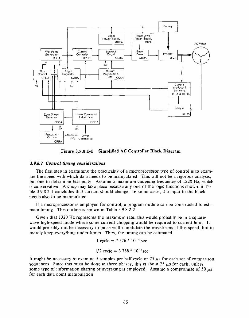
Zero Speed Detector
CPRA
Driver Command & Jerk Limit
CDCA
Driver ISD) Commands
Current Interface & Summing
CTIA & CTQA
Torque
CTOA
Figure 3.9.8.1-1 Simplified AC Controller Block Diagram
3.9.8.2 Control timing considerations
The first step m exammmg the practIcality of a microprocessor type of control IS to examme the speed with which data needs to be manipulated This Will not be a rIgorous analYSIS, but one to determme feaslblhty Assume a maxImum choppmg frequency of 1320 Hz, which IS conservative. A chop may take place because anyone of the logiC functIOns shown III Table 3 9 8 2-1 concludes that current should change In some cases, the mput to the block needs also to be mampulated
If a microprocessor IS employed for control, a program outlIne can be constructed to estImate tImmg This outlIne IS shown m Table 3982-2
Given that 1320 Hz represents the maximum rate, this would probably be m a squarewave hIgh-speed mode where some current choppmg would be requIred to current hmlt It would probably not be necessary to pulse Width modulate the waveforms at this speed, but to merely keep everythmg under lImits Thus, the tImmg can be estImated
1 cycle = 7 576 * 10-4 sec
1/2 cycle = 3 788 * 1O-4sec
It might be necessary to examme 5 samples per half cycle or 75 JLs for each set of companson sequences Smce thIs must be done m three phases, thIs IS about 25 JLs for each, unless some type of mformatlOn sharIng or averagmg IS employed Assume a compromise of 50 JLS for each data pomt mampulatlOn
86
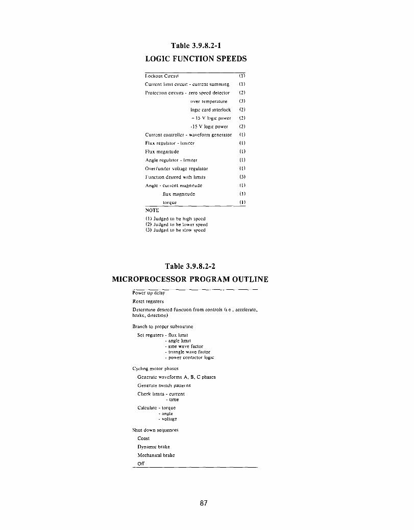
Table 3.9.8.2-1
LOGIC FUNCTION SPEEDS
Lockout CirCUIt (I)
Current IImll cIrcuIt - current summmg (1)
ProtectIOn CIrCUitS - zero speed detector (2)
over temperature (3)
logIc card mterlock (2)
+ 15 V logIc power (2)
-15 V logIc power (2)
Current controller - waveform generator (I)
Flux regulator - limIter (I)
Flux magnItude (I)
Angle regulator - limIter (I)
Over/under voltage regulator (I)
FunctIon deSired wIth limIts (3)
Angle - current magnItude (I)
flux magnItude (I)
torque (I)
NOTE
(J) Judged to be hIgh speed (2) Judged to be lower speed (3) Judged to be slow speed
Table 3.9.8.2-2
MICROPROCESSOR PROGRAM OUTLINE
Power up delay
Reset regIsters
Determme deSIred function from controls (I e , accelerate, brake, directIOn)
Branch to proper subroutme
Set regIsters - flux limIt - angle hmlt - sme wave factor - triangle wave factor - power contactor logIC
Cycling motor phases
Generate waveforms A, B, C phases
Generate SWItch patterns
Check limIts - current -time
Calculate - torque - angle - voltage
Shut down sequences
Coast
DynamIC brake
Mechanical brake
Off
87

The motor tIme constants should be exammed to see If they Impose a lImIt on the control tImmg From the motor model m FIgure 3 4.6-1b, the shortest tIme constant IS the rotorstator tIme constant whIch IS 5 156 JLs ThIs IS long compared to the mmlmum tIme needed at the hIghest possIble motor speed
Thus, the lImltmg Item IS the need for dIgItal manIpulatIOn of the vanables For each sample pomt, a number of lOgIC steps need to be Implemented The termmology for an Intel 8080 mIcroprocessor WIll be employed only to estImate processor tImmg, as shown m Table 3 9 8 2-3 Smce only about 50 JLs are aVailable and some housekeepmg functIOns (failure or mode change mterrupts) also need to be performed, thIS analysIs shows that the control requIres more than one mIcroprocessor
Table 3.9.8.2-3
MICROPROCESSOR TIMING
Cycles
Load phase current from AID converter LDA 13*
Compare regIster to accumulator CMP 4
EXIt of accumulator > regIster lP 10
Load elapsed tIme LDA 13
Compare regIster to accumulator CMP 4
EXIt If accumulator > regIster lP 10
* A-D Conversions ReqUIred Each cycle = 2 JLsec
54 cycle tImes
These estImates show that a control system sectIOned as one mIcroprocessor does not appear to be a good early entry productIOn model control element The approach taken IS to place the functIOns WhICh must be treated m an approxImately contmuous manner m analog cIrCUItry WIth appropnate control by a dIgItal mIcroprocessor Smce under these condItIons the processor need only superVIse other modules once per half cycle (all three phases) mstead of several tImes per half cycle, the work load of the processor IS reduced to performmg a sWItchmg command about once per 379/3 JLs at maXImum speed
3.9.8.3 Driver command and jerk limit (Drawing EP7644CDCA)
ThIS could be Implemented by a configurable controller as shown m FIgure 3 983-1 ThIS should be a cost effectIve solutIOn smce It reqUIres less sIlIcon area for the stored program than for a hardware Implemented lOgIC gate
88

F/R IjJ Frequency
j
~ Brake
Input Output Input Input Output ... ~ Brake
Output ~
ROM RAM ~
Input
Brake (Cooling Fan Control)
No Accelerate Output To Call
~ Input -Input 00(" Accelerate Reset
Mix Input On/Off Processor
AID 0 0 0 0 0 Input Direction
Figure 3.9.8.3-1 Driver Command and Jerk Limit Configurable Controller
3.9.8.4 Lockout and waveform generator (Drawing EP7644CLOA)
It IS proposed to make a custom mtegrated circuit (Ie) per phase for the lockout circuit functIon The custom Ie represents a reasonable cost, Yield, volume, and modularIty It needs 7 signal pms plus 3 pms for the power supply The resistors are not crItIcal and could be placed on the chip or simulated The functIOns con tamed m each custom Ie are
Dual D FlIp-Flop (2) Exclusive OR Monostable MultIvibrator 2 Input NOR
The waveform generator functIOn IS already a microprocessor ImplementatIOn and should remam so
3.9.8.5 Flux control (Drawing EP7644CFCA)
The flux regulator needs to be able to react durmg a half cycle of operation or about every 37913 J-ts The flux magnItude functIOn IS also performed by this block and may as well be left analog as the rectificatIOn would need to be performed ahead of any AID converter anyway The composite output Signal could be manIpulated digitally as there IS adequate tIme, however leavmg It an analog Signal mmimizes AID converSIOns
3.9.8.6 Angle regulator (Drawing EP7644CARA)
The angle regulator needs to be able to react dUrIng a half cycle of operatIOn or about every 37913 J-ts The mputs to thiS block are prImarIly analog as are the outputs, so It IS chosen to remam m analog form
3.9.8.7 Current magnitude, limit, and controller (Drawings EP7644CCLA and EP7644CPRA)
It would be difficult to propose a custom integrated circUlt which would have any advantage, except pOSSibly conservmg space, compared to the use of low cost commerCial mtegrated cirCUits. It IS recommended to leave thiS circuit analog, so It operates m real time
89

3.9.8.8 Zero speed detector and protective circuits (Drawings EP7644CDCA and EP7644CPRA)
This could be Implemented by a configurable controller as shown In Figure 3 9 8 8-1
Over/ Logic Under
-15VCard DC DC Logic Interlock Volts Volts
AID Input Input Input Input
RAM Output ) 5 LED Do"" Output Reset
+15 V Logic Input ROM
Brake Input
Temp Input Output On
Output SD Frequency Input Processor
00000 Output Shutdown
Figure 3.9.8.8-1 Zero Speed Detector and Protection Circuit Configurable Controller
3.9.8.9 Current interface and summing, and torque (Drawings EP7644CTIA and EP7644CTQA)
These are relatively simple CircUits to Implement USIng commercially aVailable Integrated ClfCUltS The Inputs, both current and voltage, should be normalized by proper scaling so the same modules can be employed over the total range of motor horsepower and battery system voltage It IS recommended these Inputs remaIn analog and functIOn In real time
3.9.9 Logic Power Supplies
As a best engIneenng Judgment, these power supplies should have regulated outputs ( + 5 V especially) and have good balance between ± 15 V The sum of volt amperes (or watts) needed IS 10 5, so a 20-watt supply IS picked The size of thiS supply will be Invanant with vehicle size unless an output IS employed for lights, horn, and entertaInment electrOnics The SIZIng IS based on the sWitchIng power supply study discussed earlier In SectIOn 3 9 7 2 The detaJled logic power estimates are shown In Table 3 99-1 USIng very conservative design and generous allowances for regulators, the logic power supply should be
20-watt capabJllty +15 V, -15 V center-tapped + 5 V regulated 655 cm3 (40 In 3) In volume (natural convectIOn cooling) 045 kg (1 lb) weight; 0 59 kg (1 3 lb) If extra enclosure needed
90
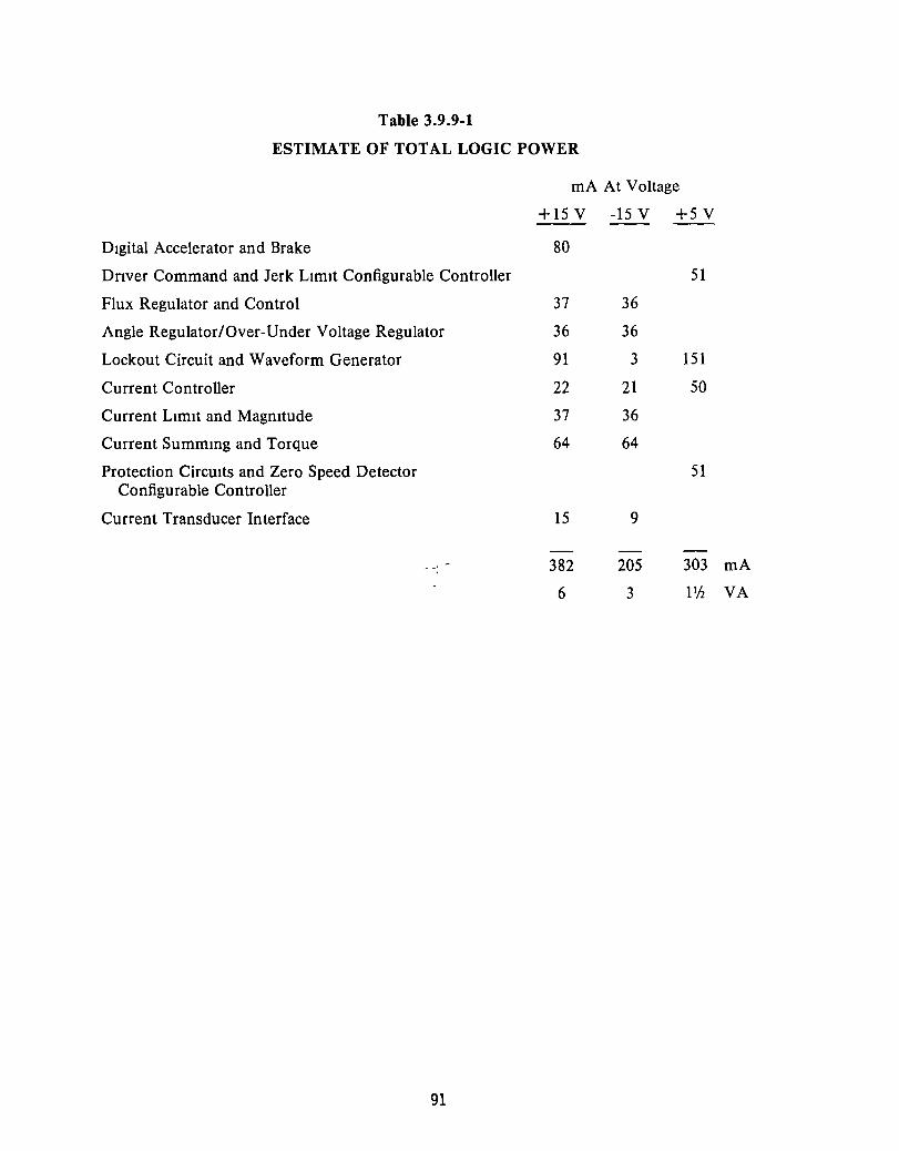
Table 3.9.9-1
ESTIMATE OF TOTAL LOGIC POWER
rnA At Voltage
+15 V -15 V +5V
DIgital Accelerator and Brake 80
Dnver Command and Jerk LImIt Configurable Controller 51
Flux Regulator and Control 37 36
Angle Regulator/Over-Under Voltage Regulator 36 36
Lockout Circuit and Waveform Generator 91 3 151
Current Controller 22 21 50
Current LImIt and Magmtude 37 36
Current Summmg and Torque 64 64
Protection CirCUIts and Zero Speed Detector 51 Configurable Controller
Current Transducer Interface 15 9
382 205 303 rnA
6 3 11/2 VA
91

3.10 CONTROLLER FAMILY LIFE CYCLE,COST ESTIMATES
A specific objective of the contract was to analytically determine life cycle cost estimates of the controller for the 10, 20, 30, 40 and 50 hp controllers desIgned In the famIly expanSIOn. The larger motors are intended to be applIcable to heavIer passenger vehIcles, delIvery vans and trucks for urban serVIce In accordance WIth the J227a -Schedule D dnvlng cycle The controller IS dIvIded Into two major portIOns, the power CIrcUIt and the sensing and control CIrcUIts.
3.10.1 Life Cycle Cost Estimates Summary
The life cycle cost estimates for the famIly of controllers at the two production levels are shown In terms of present worth (Table 3 10.1-1) and average cost per mIle (Table 3 10 1-2) The average costs per kIlometer for the base 20 hp, 108-volt system are 3 3¢ per km (5 3¢ per mIle) and 2,4¢ per km (3 9¢ per mIle) for the 10,000 and 100,000 annual productIOn levels, respectively The costs are In 1980 dollars
An objectIve of thIS development IS a sIgmficant reductIOn In the projected life cycle cost of the ac dnve system, as compared to a dc dnve system In order to fully assess thIS reduction, the two dnve systems (motor, controller and control electromcs) WIll be compared The companson WIll be made for the base 20 hp, 108-volt system in 100,000 annual productIon quantIty The factors used for thIS companson are summanzed In Table 3.10 1-3. (l,8) The economIC parameters are the same for both systems and are the same as dIscussed In Section 3 10 5 The ac system IS apprecIably lIghter, less costly, and more efficient than the dc system The projected lIfe cycle cost is 3.2¢ per km (5 1¢ per mIle) for the ac system versus 3 5¢ per km (5 7¢ per mIle) for the dc system When the fuel costs are calculated on the baSIS of the total vehIcle weIghts including the dIfference In drive system weight, the real Impact of the system effiCIency dIfference IS observed Improvements In the power Darlington transIstors and snubbers WIll reduce the Inverter losses and Increase Inverter effiCIency by 1-2%
Table 3.10.1-1
PRESENT WORTH LIFE CYCLE COST ESTIMATE SUMMARY ($)
NomInal Battery Motor Horsepower Voltage QuantIty
10 20 30 40
84 10K $2,773 $3,595 $4,421 $5,544 lOOK 2,079 2,647 3,216 4,012
108 10K 2,655 3,404 4,195 5,116 lOOK 2,003 2,510 3,066 3,713
150 10K 2,690 3,542 4,396 5,441 lOOK 2,003 2,580 3,154 3,786
300 10K 2,563 3,307 4,086 4,866 lOOK 1,920 2,416 2,937 3,480
92
50
$6,461 4,669
6,246 4,538
6,499 4,516
5,696 4,066
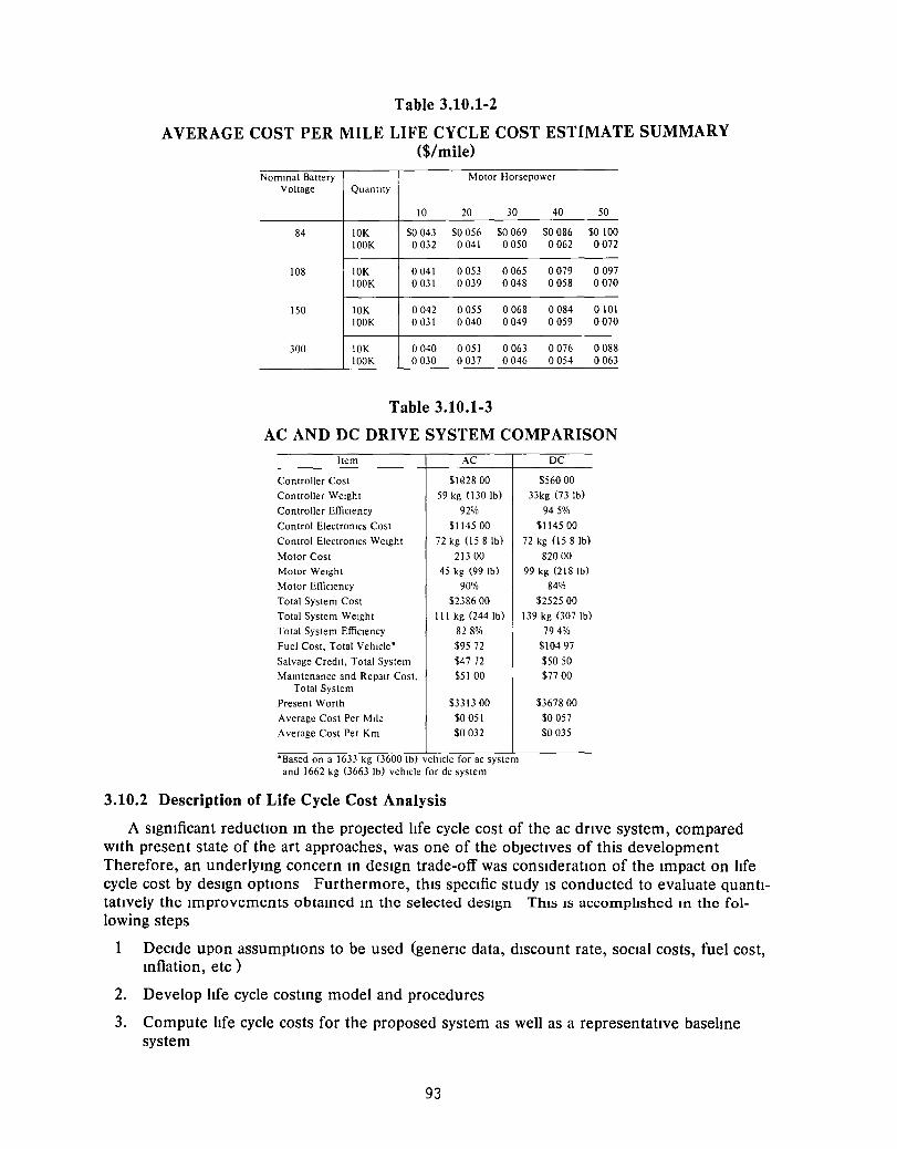
Table 3.10.1-2
AVERAGE COST PER MILE LIFE CYCLE COST ESTIMATE SUMMARY ($/mile)
NomInal Battery Motor Horsepower Voltage Quantity
10 20 30 40 50
84 10K $0043 $0056 $0069 $0086 $0100 lOOK 0032 0041 0050 0062 0072
108 10K 0041 0053 0065 0079 0097 lOOK 0031 0039 0048 0058 0070
150 10K 0042 0055 0068 0084 0101 lOOK 0031 0040 0049 0059 0070
300 10K 0040 0051 0063 0076 0088 lOOK 0030 0037 0046 0054 0063
Table 3.10.1-3
AC AND DC DRIVE SYSTEM COMPARISON
Item AC
Controller Cost $1Q28 00
Controller Weight 59 kg (130 Ib)
Controller Efficiency 92%
Control Electronics Cost $114500
Control Electronics Weight 72 kg (I5 8 Ib)
Motor Cost 213 00
Motor Weight 45 kg (99 Ib)
Motor EfficIency 90%
Total System Cost $238600
Total System Weight III kg (244 Ib)
Total System EfficIency 828%
Fuel Cost, Total VehIcle' $9572
Salvage Credit, Total System $47 72
MaIntenance and RepaIr Cost, $5100 Total System
Present Worth $3313 00
Average Cost Per Mile $0051
Average CO,st Per Km $0032
'Based on a 1633 kg (3600 Ib) vehicle for ac system and 1662 kg (3663 Ib) vehtcle for dc system
3.10.2 Description of Life Cycle Cost Analysis
DC
$56000
33kg (73 Ib)
945%
$114500
72 kg (I5 8 Ib)
82000
99 kg (218 Ib)
84%
$252500
139 kg (307 Ib)
794%
$10497
$5050
$77 00
$3678 00
$0057
$0035
A slgmficant reduction m the projected hfe cycle cost of the ac dnve system, compared w1th present state of the art approaches, was one of the objectives of this development Therefore, an underlymg concern m des1gn trade-off was cons1deratlOn of the 1m pact on hfe cycle cost by des1gn ophons Furthermore, th1S spec1fic study 1S conducted to evaluate quantitat1vely the 1mprovements obtamed m the selected deSIgn ThIS IS accomphshed ill the following steps
1 Dec1de upon assumptlOns to be used (genenc data, d1scount rate, social costs, fuel cost, mflation, etc)
2. Develop hfe cycle costmg model and procedures
3. Compute hfe cycle costs for the proposed system as well as a representative basehne system
93

Modehng assumptIOns must be made before the hfe cycle cost model can be developed or adapted The set of assumptIOns IS hsted below'
1 LIfe cycle costs wIll be computed over a base penod, whose length may be arbitranly specified but which must be the same for all candidates considered
2. All hfe cycle costs fall Into one of three categones
a The InitIal or capital cost, which IS expended at the start of the base penod and thereafter whenever the controller reaches the end of ItS economIC hfe
b A yearly recurnng cost WhICh Includes fuel and power, maIntenance and repaIrS, and (pOSSIbly) social benefits and costs
c Salvage credIt, WhICh IS attaIned at the end of hfetlme and IS cOIncIdent wIth the capItal cost for the replacement controller
3 InflatIOn affects all costs at the same rate
4 InflatIOn occurs at a constant rate per annum It IS convenIent to assume zero InflatIOn and adjust the dIscount rate accordIngly.
5 The dIscount rate IS apphed equally to all cost elements, and the dIscount rate IS constant from year to year
6 When eqUipment reaches the end of ItS economIC hfe, It wIll be replaced by sImIlar eqUipment, whose cost performance IS IdentIcal (except for InflatIOn) to those of the eqUipment beIng replaced
7. Yearly recurnng costs wIll be approxImated by a sIngle payment occurnng at midyear WhIle end-of-year payments are commonly assumed, a mIdyear representatIOn IS more accurate.
8 CapItal Investment IS amortlzed equally durIng each year of the equIpment's hfetlme, regardless of InflatIon
9 All data are assumed known wIth certainty, the life cycle cost model will be determInistIc rather than stochastIc
10 The hfe cycle costs wIll be computed over the entIre economIC hfe of vehIcles, regardless of changes In ownershIp
The first step In thIS task wIll be to reVIew these ten assumptIOns and decIde what reVISIOns, If any, should be made
A model was developed by adaptIng eXIstIng models for hfe cycle cost developed by General Electnc for tranSIt vehIcles (25,26) Two measures of hfe cycle cost WIll be avaIlable from the model the "present worth" and the average "cost per mIle" Present worth IS the amount whIch would have to be deposIted In a bank account, drawIng Interest at the dIscount rate, In order to prepay all costs of controller ownershIp and operatIon dunng a defined base penod (27) Average cost per mIle IS the amount, averaged over the defined base penod, WhICh would be paid by a vehIcle owner who pays all expenses as they occur, IncludIng amortIzatIOn of capItal costs WIth Interest at the discount rate Both present worth and average cost per mIle are vahd measures of hfe cycle cost For a gIven dIscount rate and base penod, the two measures bear a fixed ratIO
94

A general expression for present worth, P, is (25)
P=[c_sI1+e]L] o 0 l+r
1_11+e]IYIL1L l+r
l_[l+e]L l+r
+ .J1+r i Rolll+e]' l+e 1=1 l+r
where [YIL] denotes the largest Integer In the quotIent YIL, and MOD L Y denotes the remaInder In that quotient, where
Co - Capital cost pnor to InflatIOn, $
So = Salvage credit pnor to InflatIOn, $
ROI = Recurnng cost In year I pnor to InflatIOn, $
e - EscalatIOn or InflatIOn rate per annum
r - Discount rate per annum
L = Economic lIfetIme, years
Y = Base penod for present worth analysis, years
For the specIal case where recurrIng cost IS constant from year to year and where Inflation IS zero, this simplifies to
P = [c - S (1+r)-L] 1 - (1+r)-Y + R .J1+r 1 - (1+r)-Y o 0 1 _ O+r)-L 0 r
WhIle an economy Without Inflation appears unattaInable, a reasonable assumption is to adjust the discount rate to Include the effects of inflation. ThiS SimplIfied equation has an InterestIng property' the base penod Yappears only In the factor [1 - (1+ r)- Y], which may be factored out of both terms In P Thus the base penod has only the effect of changing Pby the same multIplier for any set of costs, chOIce of base period Ywill not impact the comparison between two competing controllers ThiS IS true only when recurring costs are constant (R o,-Ro) and InflatIon is zero (e = 0)
95
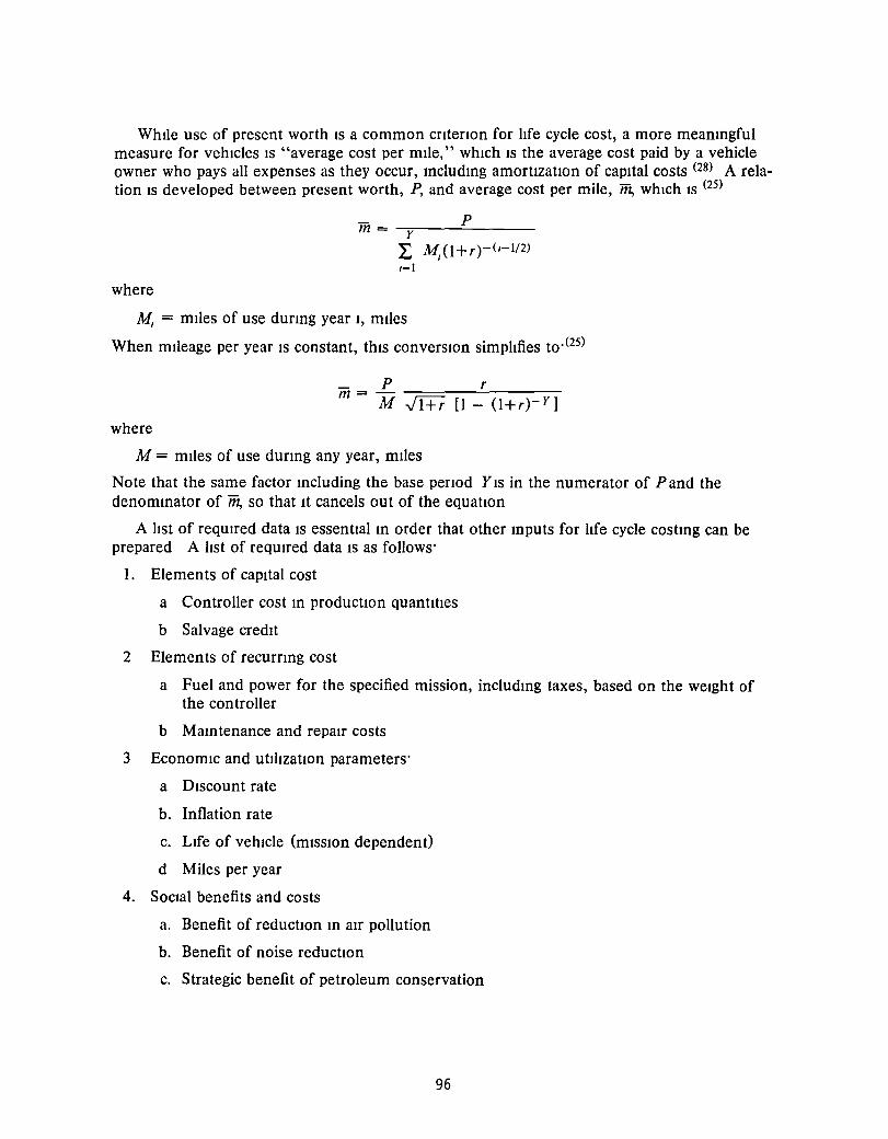
Whtle use of present worth IS a common cntenon for lIfe cycle cost, a more meanmgful measure for vehIcles IS "average cost per mIle," whIch IS the average cost paid by a vehicle owner who pays all expenses as they occur, mcludmg amortIzatIon of capItal costs (28) A relation IS developed between present worth, P, and average cost per mile, m, whIch IS (25)
m = -vy ____ ~P-------L M,O+r)-(/-l/2) 1=1
where
M, = mIles of use dunng year I, mIles
When mIleage per year IS constant, thiS converSIOn simphfies to·(25)
_ P r m=-
M v'1+r [1 - O+r)- Y]
where
M = mIles of use durmg any year, mIles
Note that the same factor mcluding the base penod YIS in the numerator of Pand the denommator of Iii, so that It cancels out of the equatIon
A lIst of reqUIred data IS essentIal m order that other mputs for lIfe cycle costmg can be prepared A lIst of reqUIred data IS as follows'
1. Elements of capital cost
a Controller cost m productIOn quantities
b Salvage credit
2 Elements of recurnng cost
a Fuel and power for the specified mission, includmg taxes, based on the weight of the controller
b Mamtenance and repaIr costs
3 EconomIc and utIlIzatIOn parameters'
a DIscount rate
b. Inflation rate
c. Life of vehIcle (mIssion dependent)
d Miles per year
4. SocIal benefits and costs
a. Benefit of reductIOn m air pollution
b. Benefit of noise reduction
c. Strategic benefit of petroleum conservation
96

AssumptIons on generIC data mcludes such factors as the dIscount rate, mflatIon rates, and fuel cost per gallon It IS convement to assume zero mflatlOn (constant dollars), wIth a compensated dIscount rate WhICh represents the dIfference between the actual dIscount rate and the general mflatlOn rate All costs are m 1980 dollars
SocIal costs and benefits comprIse a special area of generIC data. A ratIonale for establIshmg sOCial costs assocIated wIth urban transIt vehIcles are air pollutIOn, nOIse, delays, and VIsual mtrusIOn (26) Much of thIS ratIOnale IS dlfectiy applIcable to passenger vehIcles, however, ItS effects are not mcluded m thIS study
3.10.3 Elements of Capital Cost
3.10.3.1 Power circuit cost estimate summary
The power ClfCUlt components evaluated for the varIOUS motor power and battery voltage levels are
• Input filter capaCItor
• TransIstor-dIOde power module
• Power module snubber
• TranSIstor base drIve and power supply
The details of the cost analysIs for each of the above components IS gIven m AppendIx E of thIS report The cost estImate results are shown m Tables 3 103 1-1 and 3 103 1-2 and mclude mIscellaneous component costs and assembly costs SUltable deVIces are not currently avaIlable for the mput filter capaCItor reqUIred for the 300-volt system Alummum electrolytic capaCItors, as used m the baSIC deSIgn WIth adequate voltage and rIpple current ratmgs for the 300-volt system, are not currently manufactured. Rather than SWItch to a dIfferent capaCItor type, havmg hIgher cost and weIght, values for the 300-volt system are extrapolated from the lower voltage cases. A product development effort IS needed for thIS voltage range, or a system redeSIgn that WIll allow a larger rIpple current
Table 3.10.3.1-1
POWER CIRCUIT COST ESTIMATES FOR 10,000 VEHICLES/YEAR
Motor Horsepower Nommal
Battery Voltage 10 20 30 40 50
84 $1022 $1758 $2474 $3457 $4181 108 904 1567 2248 3028 3966 150 941 1709 2453 3359 4226 300 819 1480 2152 2792 3431
97

Table 3.10.3.1-2
POWER CIRCUIT COST ESTIMATES FOR 100,000 VEHICLES/YEAR
Motor Horsepower Nominal
Battery Voltage 10 20 30 40 50
84 $684 $1165 $1620 $2274 $2737 108 609 1028 1472 1976 2606 150 610 1100 1564 2053 2589 300 533 944 1356 1757 2149
TranSIstor power modules of the type requlfed for thIS Inverter do not eXIst as commercIal Items It IS felt that these modules can be deSIgned and manufactured wIth reasonable YIelds and It IS on thIS baSIS that the power module costing IS based
3.10.3.2 Control circuit cost estimate summary
In contrast to the power CIrcuIt, the control ClfCUlt IS common for all power and voltage ranges. In order to keep costs per umt as low as possIble, the costing IS based on the use of mIcroprocessor control technology The eXIstIng laboratory controller IS partItIOned such that only hIgh speed portIons of the Inverter control are performed WIth analog control components, the balance being handled WIth a mIcroprocessor or a dIgItal system
The partIcular mIcroprocessor ImplementatIOn chosen IS known as a "configurable controller." This IS a new concept wherein the mIcroprocessor and the necessary support deVIces (such as I/O ports, connectors, tImers) are Interconnected at the mask level to form a new mask for a speclahzed chIp haVing the same performance as the host deVIces The concept of the programmable controller IS to take advantage of the standardIzed eXIsting chIps yet YIeldIng many of the benefits of a custom chIp, Ie, fewer deVIces, fewer ClfCUlt board connectIOns, and lower costs.
The detaIls of the cost analYSIS for each of the control functIons IS gIven In AppendIx E of thIS report. The results of the cost estImates of any horsepower and system voltage are shown In Table 3 1032-1 These costs also Include the logIC power supply.
Table 3.10.3.2-1
CONTROL COST ESTIMATES
10,000 umts/year $1507
100,000 umts/year $1145
98
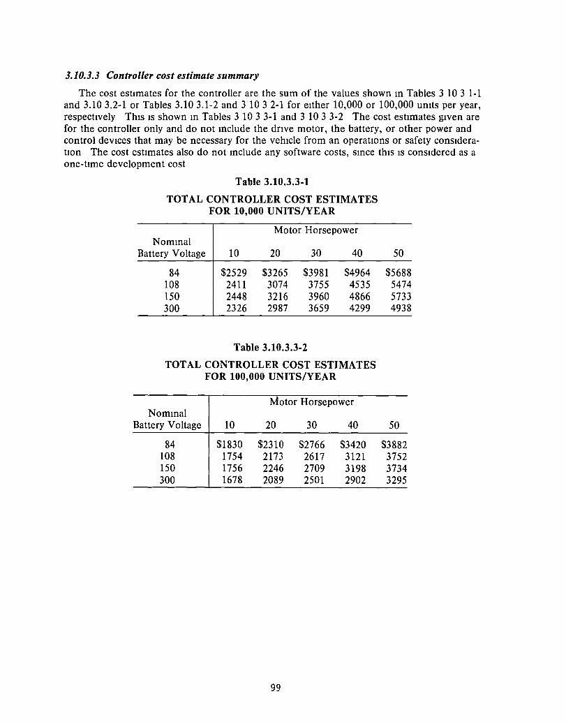
3.10.3.3 Controller cost estimate summary
The cost estImates for the controller are the sum of the values shown m Tables 3 103 1-1 and 3.103.2-1 or Tables 3.103.1-2 and 3 1032-1 for e1ther 10,000 or 100,000 umts per year, respectively Th1S 1S shown m Tables 3 1033-1 and 3 1033-2 The cost estimates glven are for the controller only and do not mclude the dnve motor, the battery, or other power and control dev1ces that may be necessary for the veh1cle from an operatlOns or safety cons1deration The cost estimates also do not mclude any software costs, smce th1S 1S cons1dered as a one-time development cost
Table 3.10.3.3-1
TOTAL CONTROLLER COST ESTIMATES FOR 10,000 UNITS/YEAR
Motor Horsepower Nommal
Battery Voltage 10 20 30 40 50
84 $2529 $3265 $3981 $4964 $5688 108 2411 3074 3755 4535 5474 150 2448 3216 3960 4866 5733 300 2326 2987 3659 4299 4938
Table 3.10.3.3-2
TOTAL CONTROLLER COST ESTIMATES FOR 100,000 UNITS/YEAR
Motor Horsepower Nommal
Battery Voltage 10 20 30 40 50
84 $1830 $2310 $2766 $3420 $3882 108 1754 2173 2617 3121 3752 150 1756 2246 2709 3198 3734 300 1678 2089 2501 2902 3295
99

3.10.3.4 Salvage Credit
Salvage credit IS Similar to capital cost and IS discounted through the controller economic hfe A salvage credit of 2% of the capital cost IS assumed representative of the type of matenals and assembhes m the controller
3.10.4 Elements of Recurring Cost
3.10.4.1 Maintenance and repair costs
The costs for repairs and mamtenance are expected to be lower for an electnc dnve system than for an mternal combustIOn engme (ICE) system The cost estimates presented here are based on prevIOus hfe cycle cost studies (25,26) Of course, these costs are only for the controller portIOn and are not constant With system horsepower as shown m Table 3 10.4 1-1 The costs are mdependent of system voltage, however
Table 3.10.4.1-1
ANNUAL MAINTENANCE AND REP AIR COSTS ($)
Motor Horsepower 10 20 30 40 50
$38 $51 $68 $90 $120
3.10.4.2 Controller weight
In order to find the fuel cost attnbutable to the controller hardware weight, the weights of the family of controllers must be estimated The weight of mverter eqUIpment used as a motor dnve has been found to follow the form In this equatIOn
W = a (HP x SR) 6 lb
where,
W = controller weight In lb
HP - controller horsepower In the constant hp regIOn
SR - constant horsepower speed range ratIO
a - 13 2 at 84 VDC
a = 124 at 108 VDC
a = 11.1 at 150 VDC
a = 64 at 300 VDC
The weight of the control electronics IS estimated as shown In Table 3.10 4.2-1 It IS the same for the family of controllers The combined weights of the controllers and control electronics is shown in Table 3 1042-2
100

Table 3.10.4.2-1
ESTIMATED CONTROL ELECTRONICS WEIGHT
Control FunctIOn WeIght WeIght (Ib) (kg)
Onver Command and Jerk LImIt (COCA) 040 o 18
Lockout and Waveform Generator (CLOA) 040 018
Flux Control (CFCA) 025 011
Angle Regulator (CARA) 030 014
Zero Speed & ProtectIOn CIrCUIts (COCA) 030 014 (CPRA)
Current LImIt (CCLA) 025 011
Torque (CTQA) 030 014
Current Transducers (CTIA) 600 272
LOgIC Power Supply 1 00 045
920 4 17
Enclosure 460 209
Interconnect Wmng 200 91
15 80 lb 7 17
Table 3.10.4.2-2
ESTIMATED AC CONTROLLER WEIGHTS
Nommal Battery Motor Horsepower Voltage
10 20 30 40 50
(Ib) (kg) (Ib) (kg) (Ib) (kg) (Ib) (kg) (Ib) (kg)
84 107 49 154 70 192 87 225 102 255 116
108 101 46 145 66 181 82 212 96 240 109
150 92 42 132 60 164 74 192 87 217 99
300 60 27 83 38 101 46 117 53 132 60
101

3.10.5 Economic Parameters
The dIscount rate, or the tIme value of money to the controller owner, IS assumed to be 10% (25,26) ThIS mcludes the effects of mflatIOn The economIC lIfetIme IS 10 years at 6,093 km 00,000 mIles) per year, whIch comcIdes wIth the requIred 100,000 J227a-D cycle lIfe (26) The base penod for the present worth analysis IS arbItranly chosen to also be 10 years, recallIng that thIS changes the present worth by a constant and does not appear m the average cost per mIle.
102

3.11 BATTERY CHARGER
The ac controller could be further Integrated Into the powertraIn for an electnc vehicle and be more useful by proVidIng the additIOnal feature of on-board battery chargIng The reqUirements for IncorporatIng this functIOn are examIned and a boost chopper design approach IS presented
3.11.1 On-Board Battery Charging
An Important Item, often overlooked In electnc vehicle studies, IS that of the battery charger Two pnmary options eXist for rechargIng the battery a statIonary garage UnIt or an on-board UnIt Both serve the same purpose, namely rechargIng the battery pack from the ac lIne
The on-board UnIt has the advantage of allOWIng the electnc vehicle the freedom of rechargIng wherever there IS an aVaIlable power source The penalty paid for thiS freedom IS the Increased vehicle weight due to the added components that must be carned around at all times Any Increase In vehicle weight causes a decrease In the vehicle range for a given battery charge Hence, the emphaSIS for the on-board charger IS clearly that of low weight, high effiCiency, and Integration Into the eXistIng Inverter hardware
The statIonary UnIt does not have thiS constraInt and It should be deSigned for the least cost system that meets the chargIng specificatIOns Only the on-board charger IS examIned In thiS sectIOn
A fundamental safety requirement for the on-board charger IS electncal IsolatIon from the power lIne ThiS enables the vehicle frame to be grounded, assurIng personal safety Without regard to the groundIng of the power supply ThiS requires a power transformer to be a part of the charger system, only systems haVIng such an IsolatIOn transformer have been conSidered
An Innovative system has been examIned In order to determIne ItS sUItablhty for thiS apphcatlon ThiS system utIhzes the maIn Inverter semiconductor components operatIng as a boost chopper for the power flow control, along With a 60 Hz transformer for voltage matchIng and electncal Isolation The system has good efficiency, however, more development work would be reqUired to estabhsh the detaIled deSign of thiS system and ItS final performance
3.11.2 Battery Charger Maximum Power Specifications
Work done on the Near Term Electnc Vehicle (ETV-l)(S) has proVided a base for estabhshIng the on-board charger specificatIOns For a 1430 kg (3150 Ib) vehicle With a 277 kg (600 Ib) payload, the energies for a full discharge of the battenes 114 km (71 mIles) of the 1227a-Schedule D cycle are
Battery output Battery effiCiency Battery input Regeneration energy Charger output Charger effiCiency Charger Input
103
186 kWh 72% 259 kWh 38 kWh
221 kWh 90% 246 kWh

If the chargmg IS done from a 230-volt lme, It IS deSired that approximately 80% of the recharge be completed m 6 hours, at which time a lower chargmg rate IS begun to avoid excessive gassmg and overcharge ThiS Will call for a per hour chargmg rate (output) of 2 95 kW For larger vehicles, the chargmg rate should be mcreased to mamtam the same 80% recharge time The chargmg rate reqUirements for the vehicles conSidered are shown below
Assumed Assumed Motor Vehicle Vehicle MaXimum Chargmg Rate
hp Weight Weight (kW) (kg) Ob)
10 681 1500 1 5 20 1362 3000 30 30 2043 4500 45 40 2724 6000 60 50 3405 7500 75
All systems Will operate from 230-volt smgle phase lme
The charger controls should operate to hold a constant current durmg the mltIal charge penod When the cell voltage reaches a hmlt value, the charge current should be reduced to hold the cell voltage of that value The hmlt voltage has been determmed to be
Vc = (292 - 0004 T) volts/cell
where TIS cell temperature expressed m OF
The final charge penod should be a low-current equahzmg charge of approximately 4 amperes, which IS mamtamed for several hours or until the vehicle IS used agam
3.11.3 Boost Chopper Approach
A schematiC dIagram of the ac controller power CIrCUIt showmg the components added to perform the battery chargmg IS shown m Figure 3 11 3-1 The baSIC charger system IS that of a boost chopper utIlIzmg the mverter power transistor and dIOde m the power module An mput 60 Hz power transformer IS reqUired for electncal IsolatIOn and for provldmg the proper voltage to the boost chopper Also, two power contactors are utIhzed one to disconnect the dnve motor dunng chargmg, and the other to connect the transformer output to two of the mverter phases Control for these contactors IS from the 12-volt auxlhary battery When the charger plug IS extended, a door SWitch (or other SUitable mterlock) energizes contactor DR which removes power from the dnve motor Battery chargmg can be mltIated from a push button which picks up contactor CH connectmg the transformer output to the mverter
The additional logiC and control for the power transistors needed to perform the chargmg functIOn IS not shown
A boost chopper reqUIres that the peak voltage of the chopper mput be less than the lowest battery voltage A fully discharged battery Will have a voltage as low as 1 3 volts per cell under load, yet ItS no-load voltage IS approximately 2 volts/cell Under chargmg conditIOns, the voltage Will nse above 2 volts/cell
104

+
BAT_ Cl-C6
~Fd T'''o CH
CH
I
AUX+rC~~~g~~ Plug Aux
1- _____________________ _
Ba tt f--r------{DR}-----!~tt
~ @)~ ~ Charger
CH Logl.c End of
- - - - - - - - - - - - - - - - - - - - - Charge -Battery Charger Addl.tl.on
DR DR
Figure 3.11.3-1 AC Controller Power Circuit with Charger
Based on an mcommg lIne voltage 10% high and a battery voltage of 2 volts/cell, the transformer secondary voltages reqUIred for the vanous battery voltages are
Nommal Battery Voltage
3.11.4 Charger Operation
84 108 150 300
Maximum Transformer Secondary Voltage (RMS)
54 69 96
192
1 ~
The active components for the charger operatIon durmg the posItive half cycle of applIed lIne voltage are shown m Figure 3.11 4-1. The pnnclple of operatIOn IS for the transistor Q\ to pass current IJ, bUlldmg up current m mductor L to a predetermmed level as shown m Figure 3.11.4-2. At that time, Q\ IS turned off and the stored energy 10 the inductor IS then transferred to the battery through dIOde D2 Via current 12 When the mductor current drops to a lower level, Q\ IS turned on agam, causmg an mcrease 10 the IOductor current and repeatmg the "choppmg" cycle
105
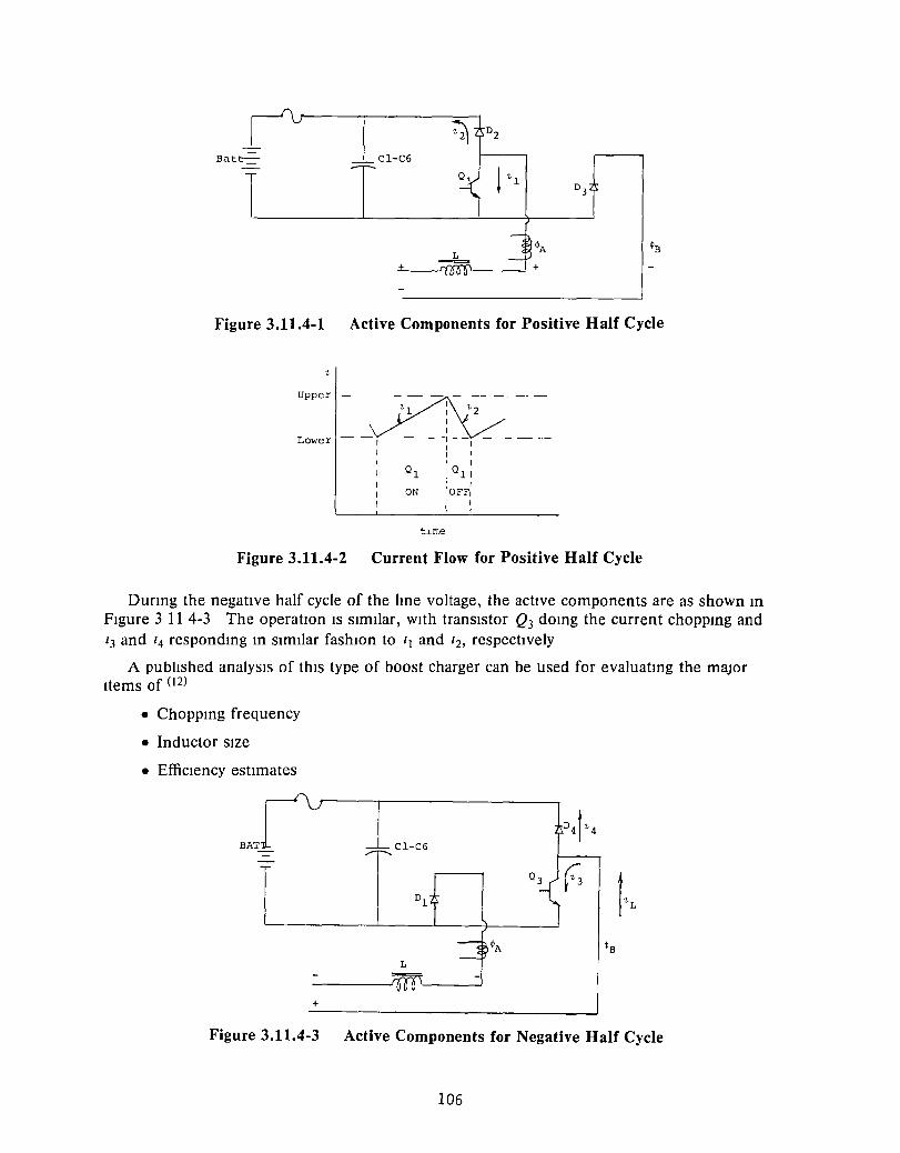
Bat~ _CI-C6
L ~ __ ---1+
Figure 3.11.4-1 Active Components for Positive Half Cycle
Upper
Lower --~~~ I ,I , "
, I Q1 ,Qll
I , ON 'OFF,
I ,
: ,
Figure 3.11.4-2 Current Flow for Positive Half Cycle
DUrIng the negative half cycle of the lme voltage, the actIve components are as shown m Figure 3 11 4-3 The operatIOn IS SimIlar, With transistor Q3 domg the current choppmg and 13 and 14 respondmg m SimIlar fashIOn to 11 and 12, respectIvely
A publIshed analYSIS of thIS type of boost charger can be used for evaluatmg the major Items of (12)
• Choppmg frequency
• Inductor SIze
• EffiCiency estimates
BAT CI-C6
D4t"4
I Q3 ~ I"L
Dl
¢A ¢B
L
----~---' +
Figure 3.11.4-3 Active Components for Negative Half Cycle
106
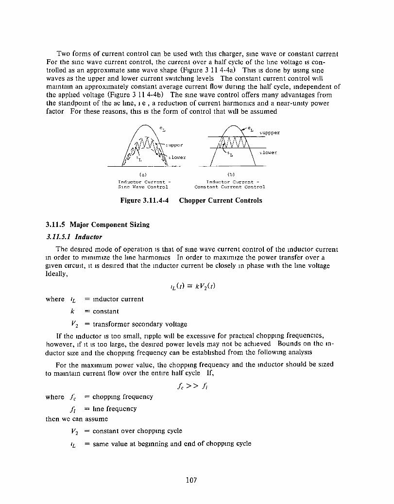
Two forms of current control can be used with this charger, sme wave or constant current For the sme wave current control, the current over a half cycle of the lme voltage IS controlled as an approximate sme wave shape (Figure 3 11 4-4a) This IS done by usmg sme waves as the upper and lower current sWltchmg levels The constant current control Will mamtam an approximately constant average current flow dUrIng the half cycle, mdependent of the applIed voltage (Figure 3 11 4-4b) The sme wave control offers many advantages from the standpomt of the ac hne, Ie, a reductIOn of current harmOnICs and a near-unIty power factor For these reasons, this IS the form of control that wIll be assumed
1-uppper -----n:-.-.-r'r--
1-lower
(a) (b)
Inductor Current - Inductor Current -Slne Wave Control Constant Current Control
Figure 3.11.4-4 Chopper Current Controls
3.11.5 Major Component Sizing
3.11.5.1 Inductor
The deSired mode of operation IS that of sme wave current control of the mductor current m order to mmlmlze the lme harmOnICs In order to maximize the power transfer over a given CIrCUit, It IS deSired that the mductor current be closely m phase With the hne voltage Ideally,
where IL = mductor current
k = constant
V2 = transformer secondary voltage
If the mductor IS too small, rIpple wIll be excessive for practical choppmg frequencies, however, If It IS too large, the deSired power levels may not be achieved Bounds on the mductor size and the choppmg frequency can be estabhshed from the followmg analYSIS
For the maximum power value, the choppmg frequency and the mductor should be Sized to mamtam current flow over the entire half cycle If,
where Ie = choppmg frequency
fi = hne frequency
then we can assume
fc»fi
V2 = constant over choppmg cycle
'L = same value at begmning and end of choppmg cycle
107
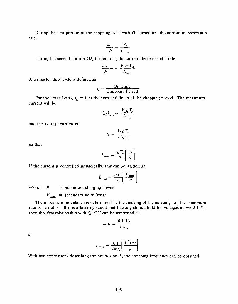
DUrIng the first portIOn of the choppmg cycle with QI turned on, the current mcreases at a rate
dt Lmm
Durmg the second portIon (Q2 turned off), the current decreases at a rate
dlL VB- V2 -=-dt Lmm
A transistor duty cycle IS defined as
On Time ~= --~~~~---
Choppmg PerIod
For the crItical case, lL = 0 at the start and finIsh of the choppmg perIod The maximum current Will be
and the average current IS
so that
L = ~ Tc I V2] mm 2 lL
If the current IS controlled smusoldally, this can be WrItten as
L = T/ Tc I Vfrms] mm 2 P
where, P maximum chargmg power
V2rms = secondary volts (rms)
The maximum mductance IS determmed by the trackmg of the current, Ie, the maximum rate of rIse of lL If It IS arbitrarIly stated that trackmg should hold for voltages above 0 1 V2,
then the dlldt relatIOnship with Q1 ON can be expressed as
or
= ~I vi rms]
Lmax 21T II P
With two expreSSIOns descrIbmg the bounds on L, the choppmg frequency can be obtamed
108

Given that
or
for 71 = 1, this Yields
ie > 107T il
This mdlcates that the choppmg frequency must be at last 31 4 times the lme frequency For a 60 Hz line, this reqUires a minimum of 2 kHz choppmg frequency
The maximum mductor size IS set by the lme conditIons of transformer voltage and chargmg power The mmlmum mductor size IS set by these same Items and the choppmg frequency (20 kHz assumed) The Inductor sizes for the battery voltage and motor horsepower ranges are shown m Table 3 11 5 1-1
Table 3.11.5.1-1
INDUCTOR SIZE RANGES (MiniMax)
Nommal Battery Voltage Motor Horsepower 84 108 150
10 0049/0516 0080/0842 o 154/1 630
20 0024/0258 0040/0421 0077/0815
30 0016/0 172 0026/0281 0051/0543
40 0012/0 129 0020/0210 0038/0407
50 0.009/0103 0016/0.168 0031/0326
300
0614/652
030713 26
0205/217
o 154/1 63
0123/1 30
Note 1 Upper figures are minimum mductance for 20 kHz choppmg frequency, lower figures are maximum mductance
2. All values In mIlhhenrIes
109

3.11.5.2 Transformer
The mput transformer IS reqUIred for voltage matchmg and electrIcal IsolatIOn of the vehicle components from the power source It IS a 60 Hz umt and ItS design can be based on conventIOnal practice DIscussIOn with eng meers m General ElectrIc's Specialty Transformer Department resulted m the welght-kV A curve for transformers m this size class (Fig-ure 3 11 52-1) This curve IS based on the core, coIl, and term mal board only, mmus any protective case This curve IS used for estImatmg the weights of the transformers for the varIOUS vehicle classes shown below
Motor MaXimum Charge Transformer Transformer Horsepower Rate Weight Weight
(hp) (kW) (kg) (Ib)
10 1 5 12 27 20 3 20 45 30 45 30 66 40 6 40 88 50 75 49 109
140 64
120 54 220V/55V - 60 HZ H
100 45
:;; ~
~ 80 36 I- en ::t:
'" """ :: 3:
60 27
40 18
20 9
1 2 5 6 7 8
RATING (kVA)
Figure 3.11.5.2-1 Transformer Weight
3.11.6 Efficiency Estimates
The major losses m the system can be estimated to give an estimate of the overall chargmg system efficiency These losses are
• Transformer - core and copper
110

• Transistor - sWitching and voltage drop
• Inductor - core and copper
• DIOde - voltage drop
• Control Power - including base dnve
3.11.6.1 Transformer
Transformers In this size range have efficiencies that tYPically are m the 97-97 5% range, with the higher efficiency bemg tYPical of the higher power ratings For this study, the transformer loss is assumed to be 3% of ratmg
3.11.6.2 Transistor switching loss
The ratio of the transistor sWltchmg loss to the total power IS, assummg a lInear sWltchmg characterIstIc, given by·(12)
Psw = .J2 Ie ~ (TR+TF) PT 7T V2rms
where Psw = sWitching loss - watts
PT = total power
Ie = choppmg frequency
En = battery voltage
V2rms = secondary volts (rms)
TR = nse time
TF = current fall tlme
Assummg tYPical values for the rIse and fall tlmes of 0 4 JLs and a choppmg frequency of 20 kHz, the power loss can be estImated Assuming the transformers are sized for the battery as discussed In SectIon 3 11 3, the ratio of Enl V2rms wIll be approximately 1 56 for all systems The transistor sWltchmg loss wIll be
Psw = 112% PT
If the recovery effects of the blocking diode (D2 or D4) m Figure 3.11 3-1 IS mcluded, the sWltchmg loss IS mcreased approximately 50% or
3.11.6.3 Transistor saturation loss
Psw = 1 68% PT
The power loss m the transistor during the conductmg period can be calculated by assumIng a fixed saturatIon voltage and Integratmg the losses over a half cycle of hne current. The ratio of the power loss to the mput power IS
PSAT = Vs [2.J2 [~l- 1]
PT En 7T V2rms
where PSAT = Transistor saturation loss in watts
Vs - Transistor saturatlon voltage drop m volts
111

ReferrIng to Figure 3 11 4-1, It IS noted that for the posItive half cycle, transistor Q\ IS In senes With dIOde D3 The loss calculatIOn should Include both voltage drops In Vs
USIng tYPical values of 1 5 volts for the transistor and 1 1 volts for the power dIOde, the saturation loss can be calculated for all the systems The ratIO of Enl V2rms IS a design parameter and constant for all systems at 1 56 Hence, the saturation loss becomes
NomInal Battery Voltage Sat Loss
84 1 25% 108 097% 150 070% 300 035%
3.11.6.4 Blocking diode loss
The blockIng dIOdes D2 and D3 (Figure 3 11 4-1) are In senes With the battery durIng the chargIng current pulse on the posItive half cycle of line voltage The conductIOn losses In these dIOdes can be calculated by an estimate of the dIOde drop
PD = VD
PT En
where PD = power loss In dIOde
VD = voltage drop across the dIOde
AssumIng a I I-volt drop for each dIOde, thiS Yields
NomInal Battery Voltage DiOde Losses
84 262% 108 204% 150 1 47% 300 073%
3.11.6.5 Inductor losses
Inductor losses will Include the core and copper losses However, assumIng the use of low-loss fernte cores, the copper loss domInates. For a properly designed Inductor, the copper loss should be kept to less than 05% of the Input power
3.11.6.6 Control power losses
The control power loss, IncludIng the transistor base dnve losses, can only be estimated until a complete control IS designed For a properly designed control, the losses should be no more than 0 5% of the rated power
112
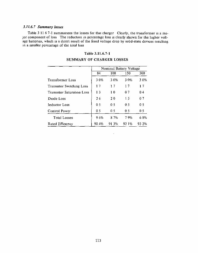
3.11.6.7 Summary losses
Table 3 11 67-1 summanzes the losses for this charger Clearly, the transformer IS a maJor component of loss The reductIOn m percentage loss IS clearly shown for the higher voltage battenes, which IS a direct result of the fixed voltage drop by sohd-state devices resultmg m a smaller percentage of the total loss
Table 3.11.6.7-1
SUMMARY OF CHARGER LOSSES
Nommal Battery Voltage 84 108 150 300
Transformer Loss 30% 30% 30% 30%
Transistor SWltchmg Loss 1 7 1 7 1 7 1 7
Transistor SaturatIOn Loss 1 3 1 0 07 04
DIOde Loss 26 20 1 5 07
Inductor Loss 05 05 05 05
Control Power 05 05 05 05
Total Losses 96% 87% 79% 68%
Rated Efficiency 904% 913% 921% 932%
113
Section 4
TEST AND EVALUATION
4.1 TEST PLAN
The tests on the ac controller are of three general types The first senes of tests venfies the operatIOn of the control system, debugs the hardware, and establIshes the desirable operatIng conditIOns for all cOmbInatIOns of Input Signal commands The second senes of tests measures the efficiencies of the motor and Inverter, the peak ac currents, and the torque output or Input as a functIon of command The third senes of tests establIshes the performance of the ac controller under duty cycle conditIons and evaluates the effects of regeneratIOn The system debug contInued throughout the tests
4.1.1 Steady-State Tests
Steady-state tests are used to establIsh the operatIng conditIOns of the motor The followIng motor measurements were made
• Flux level
• Torque per amp
• EffiCiency
• HarmOnIC losses
• Voltage and current waveforms
At up to the full load current operatIng condition, the operatIOn of the power Inverter was tested Measurements Included
• TranSistor voltages and currents
• Base current
• Inverter effiCiency
• Heat SInk temperature nse
• Sample output voltage and current waveforms
4.1.2 System Cyclic Tests
A senes of tests were performed to establIsh the operatIOn of the ac controller and motor In cOmbInatIOn as an electnc vehicle dnve system These tests were performed usmg a flywheel load to Simulate the effect of the InertIa of (approXimately) a 1600 kg (3600 lb) electnc vehicle The tests mcluded overall controller and motor system performance over the speed range of 0 to 97 km/h (0 to 60 mph) m both motonng and brakmg SpeCial attentIOn was patd to
• Startmg
• TranSItIon from pulse-width-modulatIon to square wave
• Brakmg to a stop
114

• Maximum vehicle performance
• Performance at reduced load
• Effects of battery voltage change
• Regeneration
• Low and high battery voltage protectIon
115

4.2 TEST INSTRUMENTATION
Figure 4 2-1 IS a block diagram of the ac controller, the associated three-phase mductIon motor, and vanous apparatus and mstrumentatlOn used m conductmg all tests The power measurements are made across three drIve-system boundarIes The basIc power measurements are the dc power mput to the mverter, the ac power output from the mverter, and the mechanIcal shaft power output from the ac mductlOn motor with mtegral gear box These measurements are all automated under computer control Additional measurements of lowlevel electrOnIc control system performance are also made to evaluate control system accuracy and dynamic performance Figure 4 2-2 IS a schematic diagram Illustratmg the test signal mformation flow between sensors and the computer system
The computer system performs the functIOns of test data acqulSltlOn and data processmg The ac controller logic eXists on CircUIt boards m the associated control electrOnIcs assembly, with the vehicle drIve functIOns fed to the computer A combmatlOn of analog and digital technIques are used to acqUIre and process performance data ThiS IS done usmg a hybrId computer system
The block diagram of Figure 4 2-1 shows extra mstrumentatlOn such as a wave analyzer and ac wattmeters, which are used to verIfy the accuracy of the computer controlled mstrumentatIOn
The computer program IS an mterrupt dnven, real time program which can also be used for test control, If desired, by the addition of approprIate software modules The program consists of a master background program which mterfaces With the user and prmts a data summary The routme H CONT IS executed by a fixed time mterval mterrupt every 10 mIllIseconds H CONT acqUIres the real time data and outputs real time diagnostics The block diagram (Figure 42-3) Illustrates the analog computer functIOns for power computatIOn
Figures 4 2-4, -5, and -6 Illustrate the test eqUIpment and lab setup The motor test stand (Figure 42-4) IS comprIsed of the ac controller, three-phase mductlOn motor, the load motor/generator, flywheel, torque/speed sensors, associated mstrumentatlOn, and tIe-hnes to the load motor/generator controls The mstrumentatIon panel (Figure 42-5) contams the electrIcal shunts and IsolatIOn amplIfiers used to measure the ac and dc voltages and currents Also pictured are the three current transformers, which supply ac current Signals to the computer mstrumentatlOn A general view of the hybrId computer system lab area IS seen m Figure 42-6 The hybrId computer and termmal, associated mOnItor OSCilloscope, strIP chart recorder, and vanous mstruments are seen m the picture
It should be noted that the speed measurements m thiS sectIOn always refer to the speed of the motor after the mtegral gear box reductIOn of 2 923 to 1
116
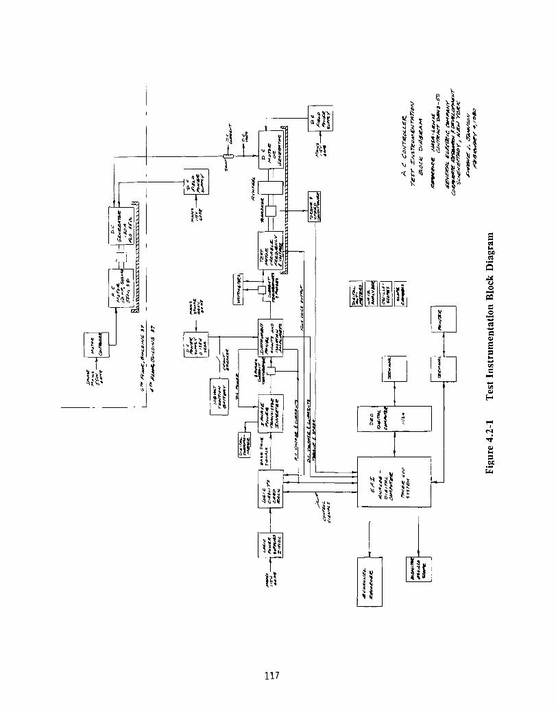
---- ---
117

D C SUPPLY
I DC A D.C ['-""-~~----<" I---l
POWER VD C A I--~
SHUNT
COMPUTERS ISOLATION AMPLIFIER
T
A.C. [ VA NOT ES : POWER ~~~"'--I-~~c.,L-
IA B C t-----!.!.L::..J..-=-....i~~~-<
~ BC
I USED TO CAPTURE DATA AND CALCULATE MOTORINVERTER PARMETERS.
3 PHASE POWER
TRANSISTOR INVERTER
-,..t;..(,'--4
YMBOL DENOTES NO. OF PHASE WIRES
CURRENT TRANSFORMERS
2. HARD COpy PRINT-OUT FOR PERMANENT RECORDS.
WATT~ETERS V
CURRENT TRANSFORMERS
3. A C. AND DC. POWER COMPUTED ON INSTANTANEOUS MULTIPLICATION OF THE APPROPRIATE VOLTAGES AND CURRENTS
WAVE ANALYZER
[
TORQUE MECHANICAL
POWER ~S~P=EE=D_--I L------I
TRANDUCERS 8 SIGNAL CONDITIONER
TEST MOTOR 3 PHASE VARIABLE VOLTAGE 8 FREQ
Figure 4.2-2 Test Signal Information Flow
118
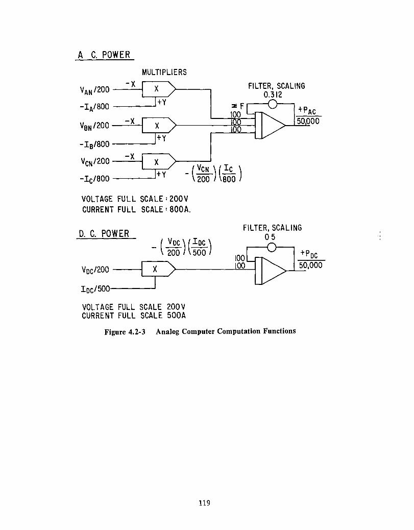
A C. POWER
MULTIPLIERS
VAN 1200 -x
-lA/BOO --_ ......
VeN 1200 -x
- Ie/BOO ___ .....J
-x
FILTER. SCALING 0.312
+PAC 50000
VCN 1200
-Ic/BOO ___ .....J ( VCN ) (IC ) - 200 BOO
VOLTAGE FULL SCALE: 200V CURRENT FULL SCALE: BOOA.
D. C. POWER _ (~) (IOC)
200 500
VOC1200 ---I L.-...-.J
loC/500-----J
VOLTAGE FULL SCALE 200V CURRENT FULL SCALE 500A
FILTER. SCALING 05
100 100
+POC 50,000 >-L...--
Figure 4.2-3 Analog Computer Computation Functions
119
, I.

I-' N o
Figure 4.2-4 AC Controller Motor Test Stand
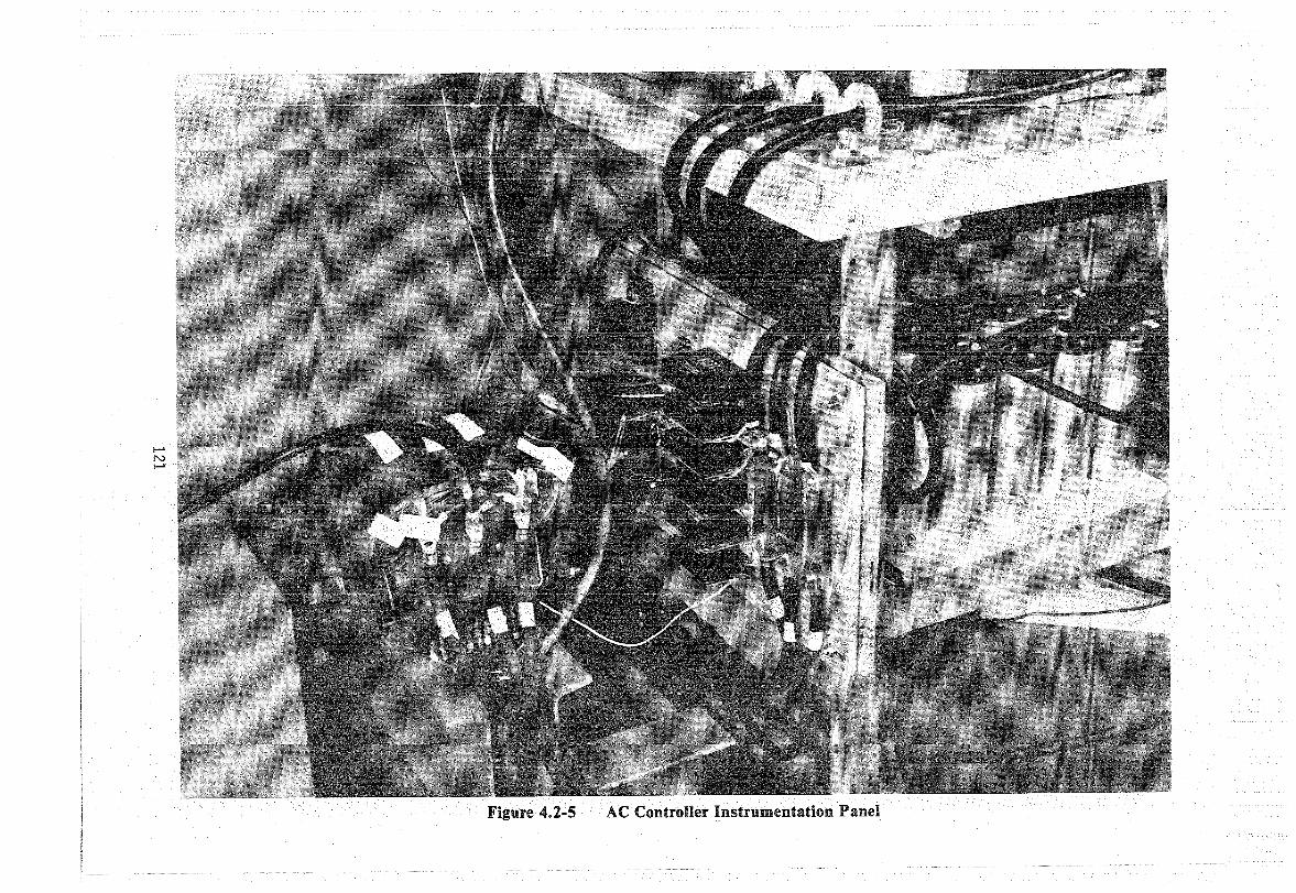
Figure 4.2-5 AC Controller Instrumentation Panel
..... N N
Figure 4.2-6 Hybrid Computer System

4.3 CONTROLLER TRANSFER FUNCTIONS
The overall dnve system block diagram IS shown m Figure 4 3-1 The system control transfer functlOns are determmed for each one of the thre.e closed loops (sm 9 eq' flux and torque) for both modes of controller operatlOn (PWM and square wave) The method for determmmg the transfer functlOns IS to open the deSired loop, remove the gam block, mJect a loop output signal and measure the resultant loop mput signal, at vanous frequencies The angle loop, sm 9 eq' IS the mner loop and IS the most Important Figures 4 3-2 and 4 3-3 show the angle loop transfer functlOn for the PWM and square wave modes, respectively Fig-ures 4 3-4 and 4 3-5 show the torque loop transfer functlOn for the PWM and square wave modes, respectively Figures 4 3-6 and 4 3-7 show the flux loop transfer functlOn for the PWM and square wave modes, respectively
(FLUX) FEEDBACK
SIGNAL
MOTOR CURRENTS
las MOTOR Ibs CURRENTS Ics
}4---__ -:--------I PROCESSING 1---SIN8eq vma AIR GAP
Vmb VOLTAGES Vmc
TORQUE COMMAND
TORQUE
Figure 4.3.1 Overall Drive System Block Diagram
123
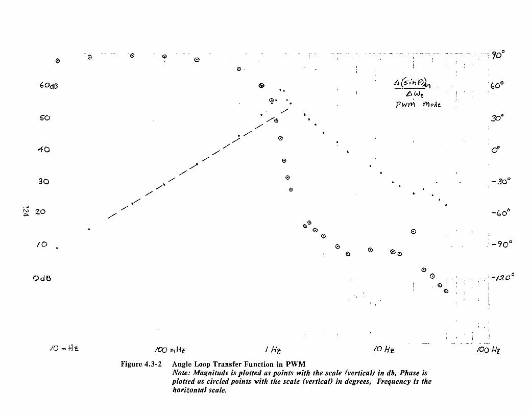
(;) 0
60dB
SO
40
30
...... ~ 20 ./'
/0
OdS
/01"'\111.
-0 Gl -
I -- -- -- - --- ------- - ----- -- ~----- - -, --~ 10°
0 0-
(i) .L1 (s-,'n e~ _ . (,0° ••
b,We I ,
0· ,
• pwm ()') o"e .-/" • • 306
./'e ./' . ./'
0 ./' ,/
0° ./' /" 0
/ /" •
./ 0 -300
./' /"
0
,./ /"
-bOo
<:> (3)
G> 0 <:>
0 _:-900
0 <:> 0 0
0 (9 _, ______ '-120°
<:>' I: ': I
G)
/CXJ III Hz / Ht /0 fir. /OO/-li
Figure 4.3-2 Angle Loop Transfer Function in PWM Note: Magnitude is plotted as points with the scale (vertical) in db, Phase is plotted as circled points with the scale (vertical) in degrees, Frequency is the horizontal scale.

>-' N U1
eOd13 (j) o o o
o o ":fO
~ o
e®
0. C!>~ ., . .~ '<
.- (i)/ • . /' .
Li(sin9)e,\ DiNe
Sq. y./qvt tvloJe
'10°
bOO
30°
.. / '\. ------- ----- ------ --.7- -m-- ~.- ------- - ----0°
./' " 50
40
30
20
•
10
Od6
/0 noH1.
,,/
./ '" ,// 0 ~
,/ e ~ / ~. " ..
e
00
" ... . . .. .. . . •
/00 '(n~~ / Hr.
e o
0j)
, (30 0 0° ~ e e(?J 10
€I e e 0 0
10 Nt
Figure 4.3-3 Angle Loop Transfer Function in Square Wave Note: Magnitude is plotted as points with the scale (vertical) in db, Phase is plotted as circled points with the scale (vertical) in degrees, Frequency is the horizontal scale.
e
-30"
-bOO
-900
, -!200
/00 f.I'l.

10m H1. /00 mHl / I-J"i.. /0 JI'l Figure 4.3-4 Torque Loop Transfer Function in PWM
Note: Magnitude is plotted as points with the scale (vertical) in db, Phase is plotted as circled points with the scale (vertical) in degrees, Frequency is the horizontal scale.
- 30 0
/00 J./2


....... N OJ
i 40d.~r- ----,
2r) -- ::--!:?
zc:
10
C.16 :-l--
-/0
-'LC i- ---
I=- _
/0 rr '-1-=
'.1) ~
. ______ ~0 ___ ,_;:___<"~--- _~ 'I I ' , - --.,-< - '1'~' -~I- r f -, 1 1,- -1-· " -1-' I' II ' I ',I, - - -I ~-< , , " '-j- '-; i I - I ' " t I ; I! l \ I I I
! ~ , '. ( - =-i --, - I
~ '300':1 , I , ,
-- -! , r., ~- e -' I ,
#-
I , - ..
f-
- - .,
, , , ' -- --......- ... ---- I_~---
, 1 ' I '
I I "I f- t - ~,-. 1 __ _ I , I I
i
I ,
I ,
-- ~ - - '- ~ r.- -, 1- --, -:...- -,- - .---- ~F_=_I·--j \;,1- I t _ I
•
I ~ :
--1 I
~ ---1-, !
, , I
- j-
,I ' r ..- -i-I 7- -. !--
I " I
I' .. '. e , .... - r·,. ,
, (i -I , I
- -;. , I
CD
'I G
, I
L.
,
-; --
o
~
(';..1 , ,i)
I , Q - --,- -;-- I
I Gl ~ - ....
; i ! ~ ~ 1-+' '--- .- ----, --r- --I If ! t I I 1 I I
, I ',-' , 1 ' , I I I: I j • ' I ---i ---,- ,-.- -~-
-, , !
--I
, , , , :
,
-l :
--,-----, . 1-- -,-- f -
!~ ---I - ----
, . ,
- t I I : t Q
L __ ~ JYl ----~---+--;_T-li i 2=to I I I J I J t I I I
: 'I~IN~ '-_~J _' _J 11 ' -- -PWfY\ ()I~e ,. ,
-,2./.rO"
i
-- ; I
i 2/')°
18()O -r--,
I 1 ;<:;",0
I I --
i --:.-,-
I
:-1 I
• , . '- ---r -,
I ! ,
-- ~ ----~-=-_'-_I-, '.- l
, , ---.- -- - ... - ., • I '
__ -.-1. _. -t
i I~/)o
_, - - - 1 - ::; I ' I I i 0' --t::"-:--- -'-+ ------ i_, : --I , !
"
I I _ I " , r - ~--------<-' ,,' 0 ':' "'" ' " - - ' '10 -r _ _1-_ t:.\!t. - -I J I I l 1- t ~--1
, I -, ---'-~L-'--- .!-,,' : - , ' :
-I I
, :.
, , I I' --- ~ -' - ---' , I ,i,' ________ l ----,- - -
_ " : ' i 0 - ---r -, : - 1_
; r, _ ___ __~_.' 0 '" ,. i - -,' . . ' ' :. . ' :-__ ,_~q;;~~~ _____ ~_~ ~ I '. ' , L.~ ~t-' : I " 'I' " /) 0 ~ -.~ ~ ~ ----' - - - J, •
I
______ 11 __ ' I I i <:) e 0 0 ,0!l ~ " " ~ " I I' I i - ____ - ____ _!! I ,!," ,
11_ I I +--l-:---r---~-~--"----rl.- i I I I I I - I 1- --t-- , : " I I ': ' ,--- --' --..:,'- 1--'-' ,0 i ' 0 -:, t:'> i' I ,I I, ' I , ' Ii, _ I ' 1 - - 'I 1- -. ,~- I __ J ,y, i ' ,
,I " ' - I . , r-- I- ' , _ ,I I I I I':' i -:-; - 0 : -,' 1-'1 _____ -" ' , !' l' 1-- -I , I ' 1 - I I
-- ------- -~.!..: 30 c
I ' I I ! i" I I I I I, I I ! I I j t 1_,
____ .... __ j~ ... , II! I __ "- __ -'-_________________ .-!..~'_L
leo v.1\-J~ ! fIt:. 10 He
Figure 4.3-6 Flux Loop Transfer Function in PWM Note: Magnitude is plotted as points with the scale (verticaL) in db, Phase is plotted as circled points with the scale (verticaL) in degrees, Frequency is the horizontal scale,
100 J..t c

...... N \0
"'dB
50
-400
30
:2.0 •
/0
Ode
/0 r\')Hi
e <:>
•
(:)
o 0 I a<!)"
0 e- ~ {~1 b.We
El:I •
e ,S". W(A.Je, yY)r>vI~
G>
e
•• ! • ,
I • -
•
• •
• •
, ,
/COm~:c • / II?:
•
<::0 ......
•
0 •
~
I{\ I' \::J )./
(!)
<:)
cfJ
i •
~ 19
J
, I
- . ..
• •
•
c:> 0 '" 0 ~ (!)
CD
I 1
1-,
IOH~
• .. •
e •
0r.\o:- ~ ""'\!,I <:10
0 i ~
Figure 4.3-7 Flux Loop Transfer Function in Square Wave Note: Magnitude is plotted as points with the scale (vertical) in db, Phase is plotted as circled points with the scale (vertical) in degrees, Frequency is the horizontal scale.
i I I __ __
- - -,2.100
I ,
2400
: 2100
I I I
1800
, 1500
, I
; -, 12.00
, , I I ,
'100
~Q
I I
:300
lOa H'i:
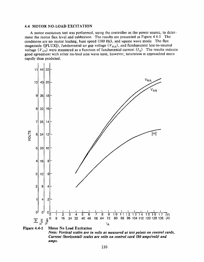
4.4 MOTOR NO-LOAD EXCITATION
A motor excItatIOn test was performed, USIng the controller as the power source, to determIne the motor flux level and cahbratlOn The results are presented In FIgure 4 4-1 The condItIons are no motor loadIng, base speed (180 Hz), and square wave mode The flux magOltude (IFLUX!), fundamental au gap voltage (VMA), and fundamental hne-to-neutral voltage (V AN) were measured as a functIon of fundamental current (J A) The results IndIcate good agreement wIth other no-load SIne wave tests, however, saturatIon IS approached more rapIdly than predIcted.
11 44 22
10 40 20
9 36 18
8 32 16
7 28 14
en ~ 6 24 12 o >
5 20 10
4 16 8
3 12 6
284
1 4 2
o 3- z «0
« ::2: > >
Figure 4.4-1 Motor No Load Excitation Note: Vertical scales are in volts as measured at test points on control cards, Current (horizontal) scales are volts on control card (80 amps/volt) and amps.
130
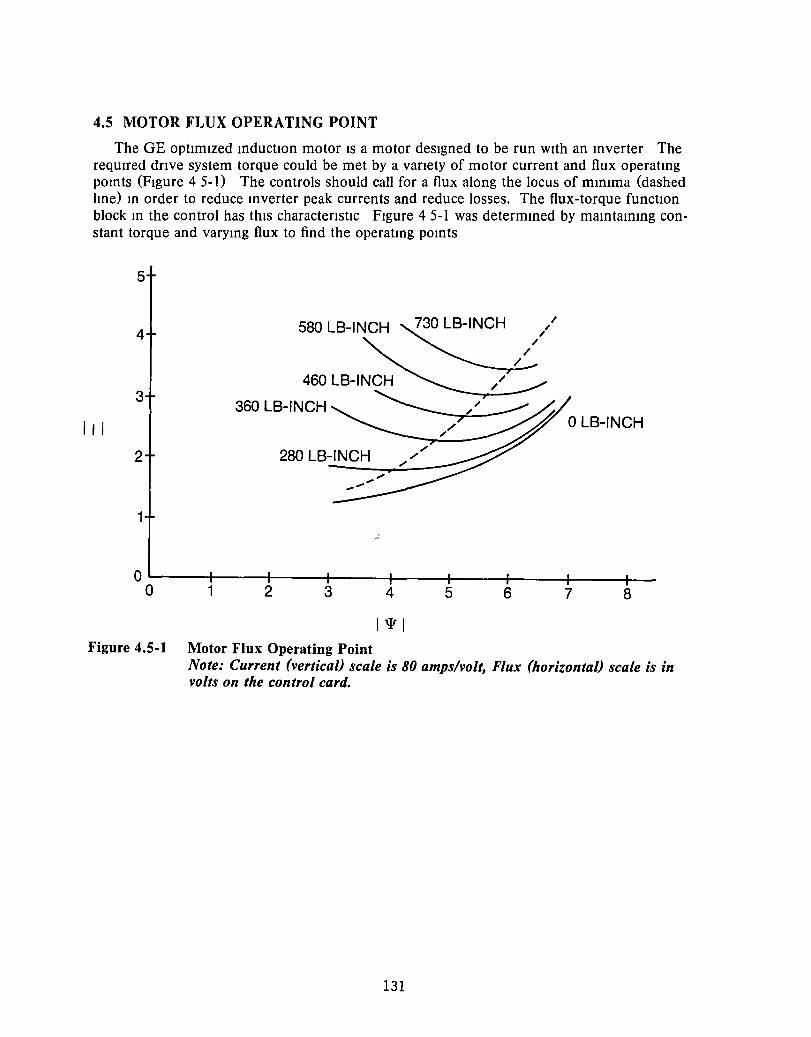
4.5 MOTOR FLUX OPERATING POINT
The GE optImIzed mductIon motor IS a motor desIgned to be run wIth an mverter The reqUired dnve system torque could be met by a vanety of motor current and flux operatmg pomts (FIgure 4 5-1) The controls should call for a flux along the locus of mmima (dashed 1m e) m order to reduce mverter peak currents and reduce losses. The flux-torque functIOn block m the control has thIS charactenstic FIgure 45-1 was determmed by mamtammg constant torque and varymg flux to find the operatmg pomts
II I
5
4
3 460 LB-INCH /'
360LB-INCH}~ 280 LB-INCH ,,/
- ""
o LB-INCH
2
1 .!
O~--~r----+----~-----r----+-----~--~-----+-o 1 2 3 4
I'l'l
5 6 7 8
Figure 4.5-1 Motor Flux Operating Point Note: Current (vertica/) scale is 80 amps/volt, Flux (horizonta/) scale is in volts on the control card.
131
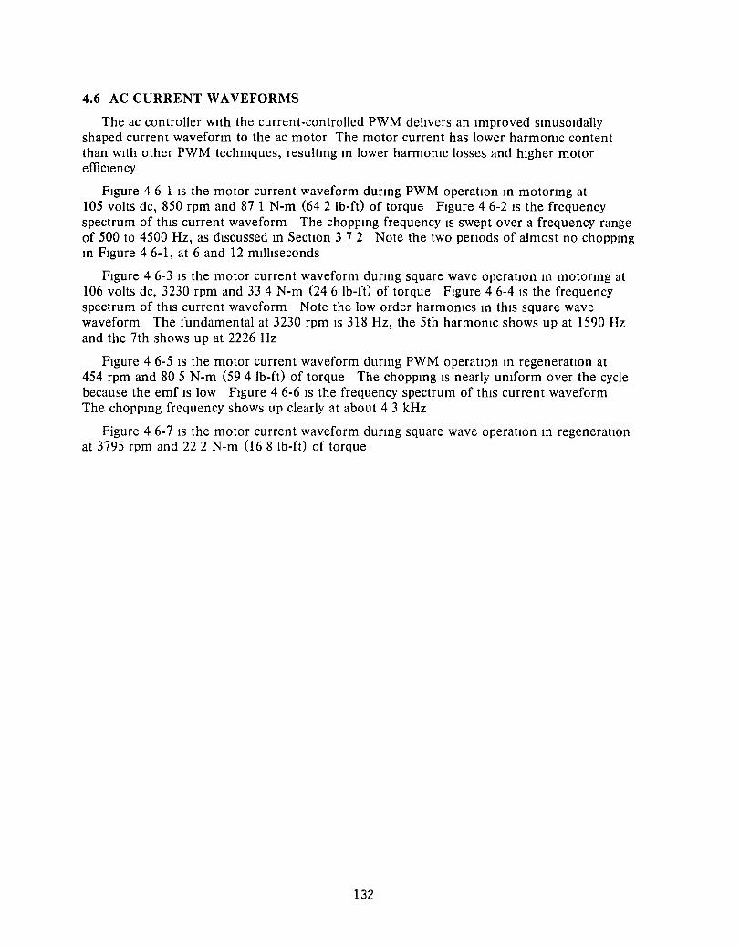
4.6 AC CURRENT WAVEFORMS
The ac controller with the current-controlled PWM dehvers an Improved smusoldally shaped current waveform to the ac motor The motor current has lower harmonic content than with other PWM techmques, resultmg m lower harmomc losses and higher motor effiCiency
Figure 4 6-1 IS the motor current waveform dunng PWM operatlOn m motormg at 105 volts dc, 850 rpm and 87 1 N-m (64 2 lb-ft) of torque Figure 4 6-2 IS the frequency spectrum of thiS current waveform The choppmg frequency IS swept over a frequency range of 500 to 4500 Hz, as discussed m SectlOn 3 7 2 Note the two penods of almost no choppmg m Figure 46-1, at 6 and 12 milliseconds
Figure 4 6-3 IS the motor current waveform durmg square wave operatIon m motormg at 106 volts dc, 3230 rpm and 33 4 N-m (246 lb-ft) of torque Figure 4 6-4 IS the frequency spectrum of thiS current waveform Note the low order harmomcs m thiS square wave waveform The fundamental at 3230 rpm IS 318 Hz, the 5th harmomc shows up at 1590 Hz and the 7th shows up at 2226 Hz
Figure 4 6-5 IS the motor current waveform dunng PWM operatlOn m regeneratlOn at 454 rpm and 80 5 N-m (59 4 lb-ft) of torque The choppmg IS nearly umform over the cycle because the emf IS low Figure 4 6-6 IS the frequency spectrum of thiS current waveform The choppmg frequency shows up clearly at about 43kHz
Figure 4 6-7 IS the motor current waveform dunng square wave operation m regeneratlOn at 3795 rpm and 222 N-m (168 lb-ft) of torque
132
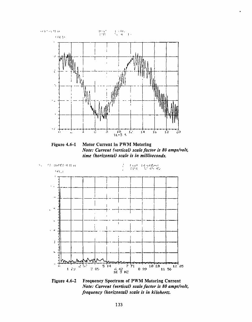
11'1' 1 I Iii, 1'1'1
-, I '.' I, I r,l -I'
Figure 4.6-1 Motor Current in PWM Motoring Note: Current (vertical) scale factor is 80 amps/volt, time (horizontal) scale is in milliseconds.
I' r I , P 1 -I -,,11(,-,1 r l r!t ~ I' • ~"'I il '_, ,---- - -=+=--, --- L ---j--+---+---f---t I I
I Ii; I 1--- ---- --+----r----t--- -i-i---+--, I I ' : I
-if---+-- 1 ; - ---1-----l-~-- -------I I \ ~ I I I I ---- -- ----,-------- -~-----t----i-- ----1---1 I I" I I
" I' ___ +-___ + ___ L_ --~-- -------f----+-- ----+---1
I ; I '--. ------l __ --!-----+--~--t---+--+---i , I
-
Figure 4.6-2 Frequency Spectrum of PWM Motoring Current Note: Current (vertical) scale factor is 80 amps/volt, frequency (horizontal) scale is in kilohertz.
133

f I 1 I ~ 1 ,- ~ I Ii J
1 11 I' I I '" 1 1 111't 1
Figure 4.6-3 Motor Current in Square Wave Motoring Note: Current {vertica/} scale factor is 80 amps/volt, time {/lOrizonta/} scale is in milliseconds. Waveform is slightly offset from zero.
I'r IIH"f' If rl ,I l' 11 ~ J "III, -,-r I I It 1 -I .1' 1 -I:
j IT I I ~---l --- ---~----- -+----+-: --+--+---i
I I I I I
1 ; I
- I I I I I I i-I
I I
--- --; --r ---- -- -,--r- ; -1 <=; - 1-- -~ --~---:--- ~---~--t- --- ----'----i----1
i I I : I I
I I I I
i I I I I I I I I ! I :
I-T--1---~--I-- i-1---I--o-l '~I
I i
II til ,:':' ..::u ~,t' :;:,0 a4 41 12 51 4 r; ] 4 1 ~l -~.:. 2!"i i' 35 98 46 .:'6
1[ ." H;-:
Figure 4.6-4 Frequency Spectrum of Square Wave Motoring Current Note: Current {vertica/} scale factor is 80 amps/volt, frequency {horizonta/} . scale is in kilohertz.
134
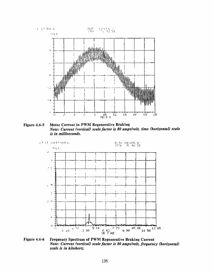
r IHT - ,.-.,1", ~ 1111 1 J ':.]
I"'L 1
Figure 4.6-5 Motor Current in PWM Regenerative Braking Note: Current (vertical) scale factor is 80 amps/volt, time (horizontal) scale is in milliseconds.
r' I F ~ "i' r r , 'f t 1 ., CII , i,.. 1 4- H' Ji, ~{ r l',t ~;:.k' ~":;l
., I I
---'----+;--~----i--~~--~--+---~
'; r--- --+--+-+--~ -~-+-I --t---i---I I I I I: I ---t----+---+- --~---+---t---t-- - ----+---1
5 - I ! - , ~--~--~ __ t-i' --+-~--~ I ! I i I I I J' i: I I
----r-- 1--+- -r---l----t---~----I---t-----i I I I I
I '
~, -1----1-i-- --r----i ___ L-
- I ' I
I ~~ -+-'~i~~~~ u~~~""""-t~~~~~~~~~~~...,..,,..p:~-,,,,,,,,~poo.j
II <_<,-;- 514 ,'71 1028 L'?85 1 c.:S 3 :35 6 42 8 99 11 56
1E 3 HZ
Figure 4.6-6 Frequency Spectrum of PWM Regenerative Braking Current Note: Current (vertical) scale factor is 80 amps/voit, frequency (horizontal) scale is in kilohertz.
135
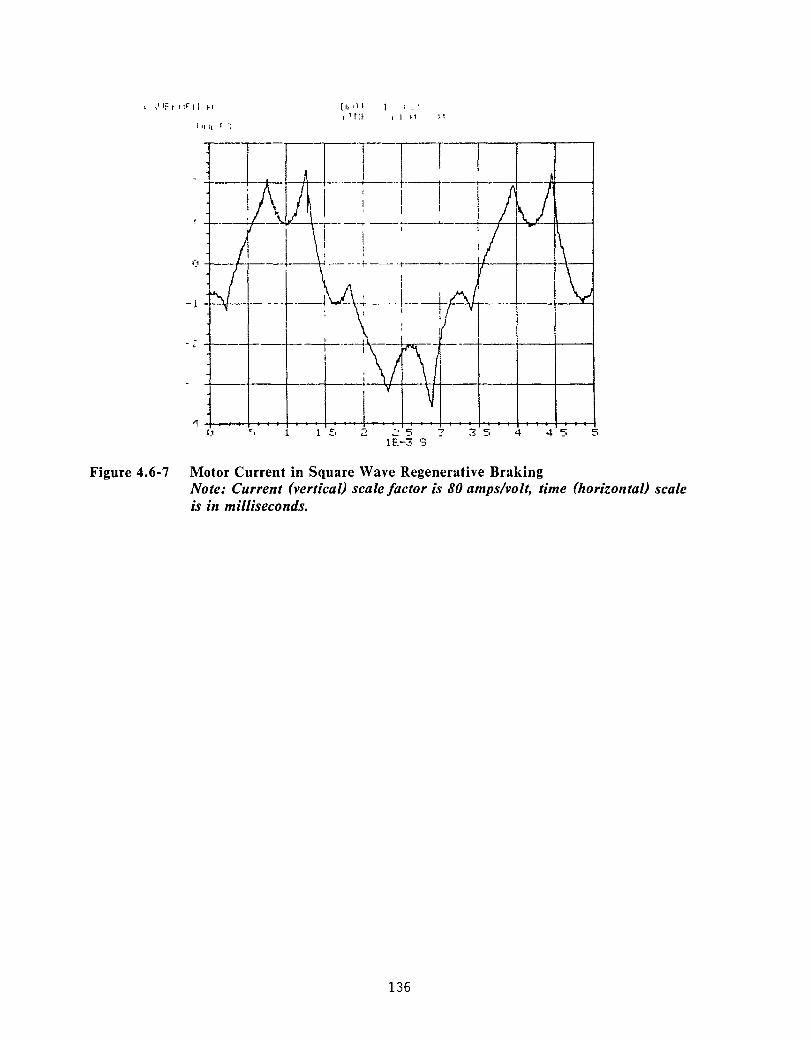
! 'I Il r ~
(1
-1
" '_1 < ,
[",11 , 'flf
f _'
I I ,1 "
-j----'T ---~~-I I I I
, - -- -I- --- -+----+-----++---+-----+-+--;
, ----r----I I
.. 2. -, '5 -;0 ~~ '" 4 4 '5 5 -' -' 110-3 ,-.
" Figure 4.6-7 Motor Current in Square Wave Regenerative Braking
Note: Current (vertica/) scale factor is 80 amps/volt, time (horizonta/) scale is in milliseconds.
136

4.7 AC VOLTAGE WAVEFORMS
The ac voltage waveforms of Interest are those In PWM operatIon, both In motoring and regenerative brakmg Figure 47-1 IS the hne-to-neutral motor voltage waveform durmg PWM operation m motonng at 106 volts dc, 1850 rpm and 664 N-m (49 lb-ft) of torque The motor air gap flux voltage waveform resultmg from the integratIOn of the aIr gap flux sensmg coIl voltage IS shown m Figure 47-2 ThIS IS the voltage at test pomt 8 on EP7644CTQA The correspondmg motor current waveform IS shown In FIgure 47-3
FIgure 4 7-4 IS the hne-to-neutral motor voltage waveform dunng PWM operatIOn m regenerative brakmg at 123 volts dc, 1850 rpm, and 556 N-m (41 lb-ft) of torque The resultant air gap flux voltage waveform IS shown m Figure 47-5 and the corresponding motor current waveform IS shown m Figure 47-6
Note the smusOldal shape of the current and flux voltage, even With the relatively few number of chops m the cycle The motor voltage has the expected quasI-square wave shape (reference FIgure 3 4 5-1) WIth the notches due to PWM choppmg
WAVEFORM C
VOLTS 5
4
,.. 3
2
1
-1
-2
-3
-4
~fo.
'"
1 2 3
II'
DATE 26-SEP-80 TIME 11 58 26
~
III
M I
4 :s 6 lE-3 S
~
7
Figure 4.7-1 Motor Line-to-Neutral Voltage in PWM Motoring
III'
1 o
Note: Voltage (vertica/) scale factor is 20 volts/volt, time (horizonta/) scale is in milliseconds.
137

I~A\)EFORt'l B
(}OLTS
D~ITE 26-SEP-60 TUIE 11 58 13
15~---r--~~--~---r--~~--~---r---'----~--'
lO4----+---4~--+_--_r--~----+_--~--~----r_--,
1 2 3 6 9
Figure 4.7-2 Motor Air Gap Flux Voltage in PWM Motoring Note: Voltage (vertical) scale is ill volts, time (horizontal) scale is in milliseconds.
11Al.JEFOF:t'l A
~JOLTS
5
4
J
D~lTE <:6-::;EP-80 TUIE 11 52 00
~ n~ 1 I\N v
l
1
I
~ ~ , (¥ \.
'1 1
V
I"" \
\J ~
-1
-2
-3
-4
-5 1 2 3 4 5
lE-3 S
Figure 4.7-3 Motor Current in PWM Motoring
6
~ \
1\ ~ \
l,
7 9 ~ 1 e
Note: Current (vertical) scale factor is 80 amps/volt, time (/lOrizontal) scale is in milliseconds.
138

l)OL T'3
6
4
2
-2 .&.
r
-4 0 1 2 3
D~ITE. ~E"-SEP-80 TINE 11 54 16
~ I
4 :5 6 lE-3 S
7 e ~ 1 8
Figure 4.7-4 Motor Line-to-Neutral Voltage in PWM Regenerative Braking Note: Voltage (verticalJ scale factor is 20 volts/volt, time (horizontalJ scale is in milliseconds.
I)OLTS
[lHTE 26-SEP-E'Lj TItlE'" 11 38 03
10'-~~----r----r--~----~~~----r---~--~--~
0;----+--~+_--~--~~--4_--_+--_4~--~--_4~~
-5;----+----++--~--~----4_--_+----~~~--~~~
-10;----+----+_--~--~~--4_--_+----~--~L-_4--~
1 2 3 4 ~ 6 lE-3 S
7
Figure 4.7-5 Motor Air Gap Flux Voltage in PWM Regenerative Braking
18
Note: Voltage (verticalJ scale is in volts, time (horizontalJ scale is in milliseconds.
139
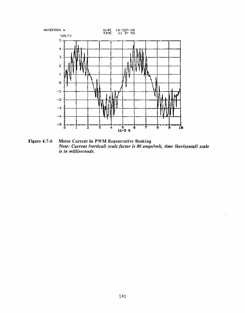
Wll)EFORtl H
IJOL T3
5
3
2
1 I~ II.
'\ \ ~
-1
-2
-3
-4
-5 1 2
~
3
OHTE ,'6-'3EP-E:O TIr1E 11 37 50
II
t J
4 5 6 lE-3 S
~
'\ -'1
~
?
Figure 4.7-6 Motor Current in PWM Regenerative Braking
M~
V
~ 1 e
Note: Current (vertical) scale factor is 80 amps/volt, time (horizontal) scale is in milliseconds.
140

4.8 POWER MODULE WAVEFORMS
The power module voltage (collector-emItter) and current (total collector) durmg sWltchmg, especially turn-off, are of particular mterest. The voltage and current waveforms were taken dunng PWM motormg operatlOn at 600 amps peak WIth a 110 volt dc bus The voltage at the turn-off of 600 amps IS shown m FIgure 4 8-1 The peak overshoot voltage IS 240 volts The current at turn-off IS shown In FIgure 4.8-2 The current fall time (90% to 10%) IS about 1 5 mIcroseconds
The power module base dnve current for one cycle of square wave motonng operatlOn IS shown In FIgure 4 8-3 The figure shows both the forward current (between 3 and 4 amps) dunng the conduction time (0.8 mIllIseconds) of thIS half-phase of the mverter and the reverse current spIke at turn-off (3 7 amps) to InItiate the off time of thIS half-phase FIg-ure 4 8-4 IS an expanded VIew of the current at turn-on shOWIng the nse of the base current m about 0 5 mIcroseconds FIgure 4 8-5 IS an expanded VieW of the current at turn-off showing a peak reverse current of 39 amps and a total turn-off time (IncludIng storage time) of about 4 mIcroseconds (measured from zero crossmg to abrupt change m reverse current)
WiUEFOPrl A
I.IOLT'::;
250
150
100
50
J -513
( J 1\
1
/ I
2 4
D~iTE 4-SEF'-80 T Jt1E 1 ~\ 133 2(1
, >
1 If' --\J'
6 8 113 12 14 16 1E-6 S
Figure 4.8-1 Power Module Voltage at Turn-off in PWM Motoring
18 2 e
Note: Voltage (vertical) scale is in volts, time (horizontal) scale is in microseconds.
141

l'filE 1 [tH. ~1 <1' "~,:
.1.1
Ll I
lr_\ I
\ \ I I
1 ::
1':-,
14
\ \ I
10
N \ ~
..:'
4
- 4 :. ~_ - " 10 lE"6 S
Figure 4.8-2 Power Module Current at Turn-off in PWM Motoring Note: Current (vertical) scale factor is 40 amps/millivolt, time (horizontal) scale is in microseconds. Actual zero current is at 3 millivolts in waveform.
I~Ht)EFOR~l A
lE-3 ')OL1S
50
40
30
20
10
-10
-20
-30
-40 2 4 6
DATE 29-AUG-E:1) Tl t1E 1 i;:1 2'3 :?9
f'-
8 1 1 2 1E-3 S
,..
1 4 1 6 1 8 2
Figure 4.8-3 Power Module Base Drive Current in Square Wave Motoring Note: Current (vertical) scale factor is 1 amp/lO millivolts, time (horizontal) scale is in milliseconds.
142
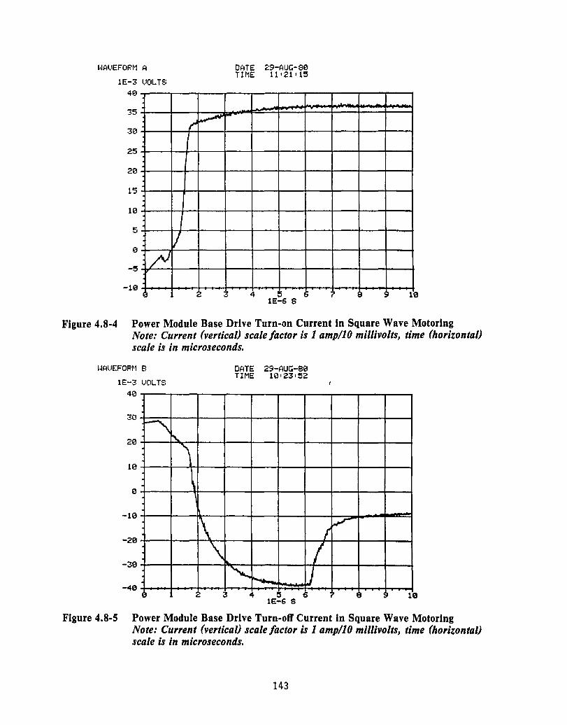
~l~ll,JEFOP.~l A
lE-3 l)OL TS: 40
'35
30
25
1'3
10
-5 ~ -Ie
/
~ r-I
<OJ 4 :; 6 1 o 1E-6 S
Figure 4.8-4 Power Module Base Drive Turn-on Current in Square Wave Motoring Note: Current (vertical) scale factor is 1 amp/IO millivolts, time (horizontal) scale is in microseconds.
I~Al.JEFOFi'r'l I:)
1E-3 VOLTS 40
30 , 20
10
-10
-20
-30
-413
"\.
'\
, \
l\ \
:3
~ I
/ " ~ 4 :;
1E-6 S 6 1 o
Figure 4.8-5 Power Module Base Drive Turn-off Current in Square Wave Motoring Note: Current (vertical) scale factor is 1 amp/IO millivolts, time (horizontal) scale is in microseconds.
143
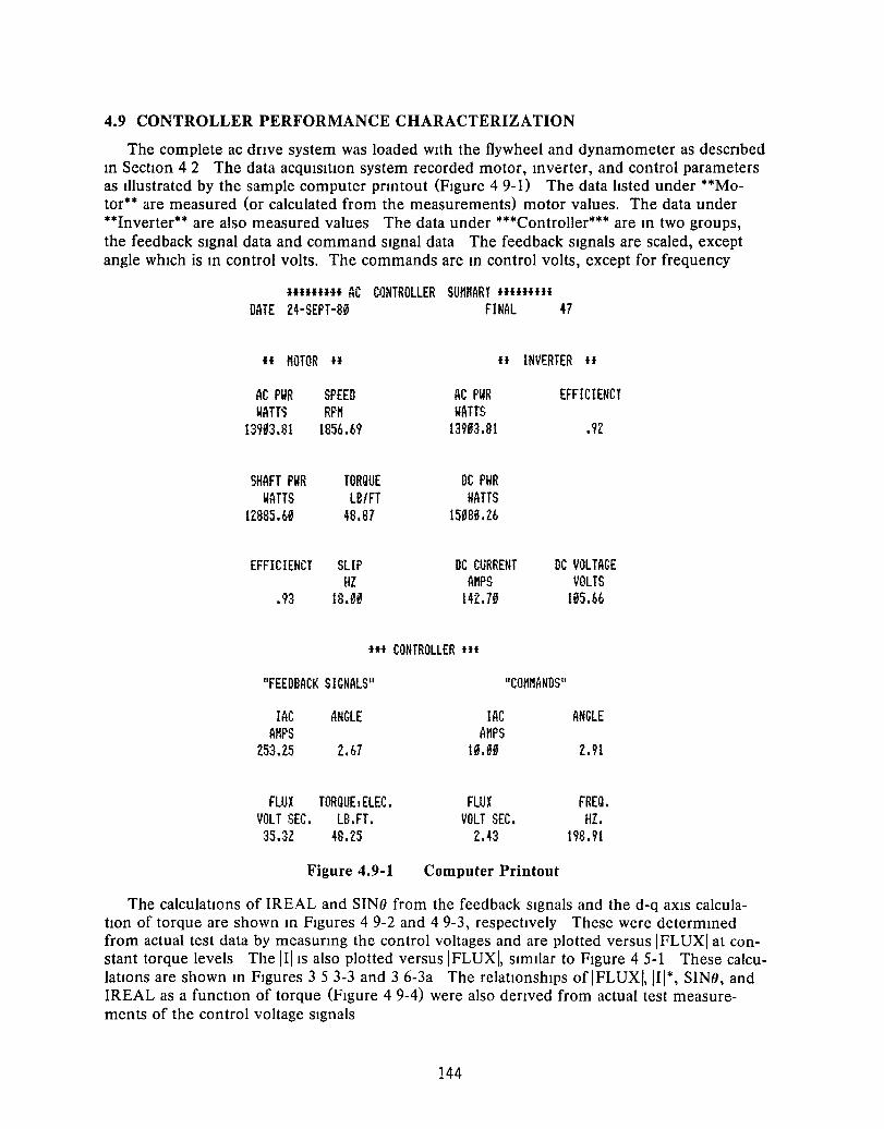
4.9 CONTROLLER PERFORMANCE CHARACTERIZATION
The complete ac dnve system was loaded wIth the flywheel and dynamometer as descnbed m SectlOn 4 2 The data acqUlsitlon system recorded motor, mverter, and control parameters as Illustrated by the sample computer pnntout (FIgure 49-1) The data hsted under **Motor** are measured (or calculated from the measurements) motor values. The data under **Inverter** are also measured values The data under ***Controller*** are m two groups, the feedback sIgnal data and command sIgnal data The feedback sIgnals are scaled, except angle WhICh is m control volts. The commands are m control volts, except for frequency
HlffHH AC CONTROLLER SUMMART ffffffff!
DATE 24-SEPT-80 FINAL 47
H HOTOR H If INVERTER H
AC PWR SPEED AC PWR EFFICIENCT WATTS RPM WATTS
13993.81 1856.69 13903.81 .92
SHAFT PWR TORQUE DC PWR WATTS LB/FT WATTS
12885.60 48.87 150B0.26
EFFICIENCY SUP DC CURRENT DC YOLTAGE HZ MIPS VOLTS
.93 18.00 142. 70 IS5.66
Iii CONTROLLER III
"FEEDBACK SIGNALS" "COMMANDS"
lAC ANGLE lAC ANGLE AMPS MIPS
253.25 2.67 IS.00 2.91
FLUX TORQUE,ELEJ:. FLUX FREQ. VOLT SEC. LE.FT. VOLT SEC. HZ. 35.:32 48.25 2.43 198.91
Figure 4.9-1 Computer Printout
The calculatlons of IREAL and SINO from the feedback SIgnals and the d-q aXIS calculatlOn of torque are shown In FIgures 4 9-2 and 49-3, respectlvely These were determmed from actual test data by measunng the control voltages and are plotted versus IFLUXI at constant torque levels The III IS also plotted versus IFLUXI, SImIlar to FIgure 45-1 These calculatlons are shown m FIgures 3 5 3-3 and 3 6-3a The relatlOnships of IFLUXI, 111*, SINO, and IREAL as a functlOn of torque (FIgure 49-4) were also denved from actual test measurements of the control voltage SIgnals
144

III T (I W 1- K II I) = IREAL
T = SINO (IWI-KIII)III
4
Vi ~ 0 2:-
3
Figure 4.9-2
4
IIIAT - 360 LB-INCH 3 en - 460 LB-INCH
III AT ~ - 208 LB-INCH 0
2:- 2
IREAL AT - 360 LB-INCH
IREAL AT - 208 LB-INCH
5 6 7 3 4 567 I FLUX I (VOLTS) I FLUX I (VOLTS)
Real Current Computation Figure 4.9-3 Angle Computation Note: IREAL andlJi (vertica/) scales are in control volts, IFLUX! (horizonta/) scale is in control volts.
Note: SINO (vertica/) scale is in control volts, IFLUX! (horizonta/) scale is in control volts.
Figure 4.9-4
7 (V)
6
" 5
-3
-4
-5
-7
1'1'1
III'
7 8 9 10 T(V)
SCALING
TORQUE 128LB-FTN 1'1'1 622VRMSN III 7132AN
T RATED = 48 3 (LB-FT) ~ 3 79V T PEAK = 1226 (LB-FT) ~ 9 58 V
Control Functions Related to Torque
145

The torque-speed curves of Figure 4 9-5 are plotted from test data, with the motor flux voltage and motor current also shown The torque and speed are at the gear box shaft after the 2 923 1 reductIOn The current IS the average of the three-phase full-wave rectified ac motor lme current The flux IS scaled from the controlled voltage Three cases, A, B, and C, are shown for the three different accelerator commands, demonstratmg the part-throttle drIve system performance Case B IS the J227a-D cycle 26 hp reqUIrement Case A IS a higher power level (about tWice-rated torque) and Case C IS a lower power level (about half-rated torque) The rated torque at the gear box shaft IS 660 N-m (487 lb-ft) at 1833 rpm, Ie, 17 hp. Case C shows that 37 N-m (27 lb-ft) of torque could mamtam up to 3700 rpm, With a current of 180 amps and a flux voltage of 27 volts In Case B, the 73 N-m (54 lb-ft) of torque IS held up to 2500 rpm, With 270 amps and 33 volts flux, the flux then begms to decrease and the output IS lImited to 26 hp In Case A, the flux IS lower than deSired between 1200 and 2500 rpm due to the motor approachmg saturatIon The torque output follows thiS flux With a current between 420 and 370 amps A 35 hp lImit IS reached at 2700 rpm The reductIon of flux at reduced torque levels by the controls IS apparent from thiS graph (reference SectIOn 3 6 5)
90
80
70
60
40
30
__ IA
-------L ---.-.~ '+'A --------
~ 'I' _._._._~,_ -< 8
TORQUE (T) CURRENT (I) FLUX ('1')
CASES A, B, C
....... '\. r---------~----~~~~'I'c
~~.:--.. 18 ,," 'I'
20 ----------r--..:.. ....... -L A
10
o 3000 SPEED (RPM)
4000 5000
Figure 4.9-5. System Torque-Speed Performance
146
4.10 CONTROLLER LOSS SEPARATION
The pnnclpal IndIVIdual controller losses were measured or calculated at four operatIng condItIons, for WhICh the total controller, motor, and system parameters were measured wIth the data acqUIsItIon system (Table 4 10-1) The operatIng condItIons were In the PWM and square wave modes In motonng and regeneratIve brakIng Note that the measurement WIth the data acqUIsItIon system does not Include the 12-volt auxIlIary power loss (control electronICS and base dnves), but does Include the blower loss These two losses have almost the same value (Table 4 10-1) SInce the blowers were oversIzed and were Included only In regard to the engIneenng model system, the InclUSIOn of their losses accounts very well for the base dnve and control electronIcs losses
The pnnclpal controller losses are lIsted In Table 4 10-1 The controller losses Include some constant losses (Independent of power level, etc) and vanable losses The vanable losses depend not only on power level, but also on ac motor frequency, choppIng (PWM) frequency, dc voltage, and ac current magnItude The behavIOr of the losses IS dIscussed more fully In SectIOn 4 11 The loss separatIon results In Table 4 10-1 are In good agreement WIth the total Inverter loss measured by the data acqUIsItIon system The small dIfferences between them were Included as mIscellaneous loss, WhICh were due to conductor loss, fuses, contacter/relay coIls, etc The power module sWItchIng loss and snubber loss are observed to be hIgher In PWM than In square wave, due to the hIgh choPPIng frequency The power module conductIOn loss depends basIcally on the ac motor current magnItude The base dnve loss IS somewhat hIgher In square wave because the transIstors are dnven for a complete half-cycle
Refernng to the separate losses In Table 4.10-1, a few observatIOns about losses can be made The power module conductIOn loss could be reduced by raIsing the battery system voltage to reduce the motor rms current, thus redUCIng the rms transIstor and dIode current ThIS would also reduce other current-related losses Faster sWItchIng transIstors and dIodes could reduce the combIned snubber and sWItchIng losses TransIstors WIth a hIgher voltage ratIng (larger SOA) could reduce the SIze of the snubber capacItors, thus redUCIng the snubber loss
147
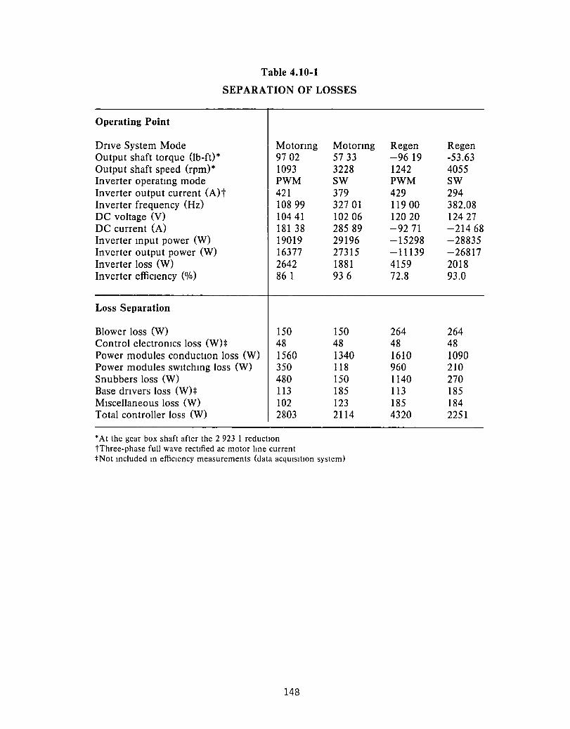
Table 4.10-1
SEP ARATION OF LOSSES
Operating Point
Dnve System Mode Motonng Motonng Regen Regen Output shaft torque Ob-ft)* 9702 5733 -9619 -53.63 Output shaft speed (rpm)* 1093 3228 1242 4055 Inverter operatmg mode PWM SW PWM SW Inverter output current (A)t 421 379 429 294 Inverter frequency (Hz) 10899 32701 11900 382.08 DC voltage (V) 10441 10206 12020 12427 DC current (A) 181 38 28589 -92 71 -21468 Inverter mput power (W) 19019 29196 -15298 -28835 Inverter output power (W) 16377 27315 -11139 -26817 Inverter loss (W) 2642 1881 4159 2018 Inverter efficIency (%) 86 1 936 72.8 93.0
Loss Separation
Blower loss (W) 150 150 264 264 Control electrOnIcs loss (W):f: 48 48 48 48 Power modules conductIOn loss (W) 1560 1340 1610 1090 Power modules sWItchmg loss (W) 350 118 960 210 Snubbers loss (W) 480 150 1140 270 Base dnvers loss (WH 113 185 113 185 Miscellaneous loss (W) 102 123 185 184 Total controller loss (W) 2803 2114 4320 2251
* At the gear box shaft after the 2 923 1 reductIOn tThree-phase full wave rectified ac motor lIne current :j:Not Included In effiCiency measurements (data acquIsItion system)
148
4.11 EFFICIENCY MAPPING
Among the most Important senes of tests are the watts loss and efficiency mappIng of the ac controller and ac dnve system (motor and controller) The loss results for the controller motor and dnve system In the motonng and regeneratIve braking modes are presented The results are In the form of the watts loss versus motor current at vanous speeds The motor current IS the average of the three-phase full-wave rectIfied ac lIne motor current The speed IS at the gear box shaft after the 2923'1 reductIOn. The analysIs of avaIlable test data from the data acqUIsItIon system (reference Figure 4.9-0, In terms of loss, results In a quahtatIve as well as quantItatIve understandIng of the loss mechanIsms and trends The controller loss does not Include the 12-volt auxIlIary power loss (control electronics and base dnves, 161 watts to 233 watts), but does Include the blower loss (150 watts In motonng, to 264 watts In regeneratIve brakIng) The motor loss Includes the gear box loss The dnve system loss Includes the controller, motor, and gear box losses Rated torque at the gear box shaft IS 660 N-m (487 Ib-ft) at 1833 rpm, Ie, 17 hp
The controller, motor, and dnve system losses for motonng operatIon are shown In Figures 4 11-1, -2, and -3, respectIvely DependIng on the current and speed, the dnve system may be operatIng In the PWM or square wave mode. Below base speed (1833 rpm), the drive operates In PWM regardless of the current, but as the speed Increases, the dnve transItIons to square wave Because the flux level in the motor IS varied as a functIOn of torque, this transItIOn does not occur at the same speed. At low currents, the dnve operates In PWM up to relatIvely high speeds, but at high currents the dnve transitions to square wave at base speed The controller loss (Figure 4 11-0 in PWM decreases with IncreaSIng speed (for a constant current) as the controller drops the number chops, then the loss In square wave increases with IncreasIng speed as the frequency Increases The loss Increases with IncreasIng current (for any constant speed) The controller loss has several components constant loss (blowers, etc), loss proportIOnal to current (conductIOn), loss proportIOnal to current squared (conductIon, parasItIc resistance), loss proportIonal to current and frequency (switchIng), and loss proportIOnal to current squared and frequency (snubber) The motor loss (Figure 4 11-2) IS less well behaved than the controller, but baSically Increases with IncreaSIng speed In PWM and remaInS fairly constant with speed In square wave In square wave, the fnctlOn and WIndage loss Increases with speed, but IS partIally offset by the reduced core loss as the flux level decreases The motor loss Increases with IncreaSIng current (for any constant speed) The motor loss is composed of loss due to fnctlOn and WIndage, stray load loss, core loss, stator and rotor resistance loss, harmOnIC core loss, harmOnIC current resistance loss, and gear box loss. The dnve system loss (Figure 4.11-3) IS the additIon of the controller and motor losses
The controller, motor, and dnve system losses for regeneratIve brakIng operation are shown In Figures 4.11-4, -5, and -6, respectively The transItIon from PWM to square wave occurs at a higher speed because the voltage IS higher. The controller loss behaves simIlarly to motonng operatIOn, but IS somewhat larger due to the higher dc voltage and, In PWM, to the higher choppIng frequency since the counter emf is small These Increases are partIally offset by the lower conduction loss because the dIodes carry more current The motor loss behaves simIlarly to motonng operatIOn but IS somewhat lower due to lower slip
The effiCiency results for the controller and dnve system In the motorIng and regeneratIve brakIng modes are presented The results are presented In the form of the effiCiency versus torque at vanous speeds The torque and speed are at the gear box shaft after the 2 923.1 reductIOn
The controller and dnve system effiCiency for motonng operatIOn are shown In Fig-ures 4 11-7 and -8, respectIvely The effiCiency falls off rapidly at low torques and speeds, due
149
to the fixed losses (not a functIOn of load) The peak controller efficiency of 95% occurs at 3000 to 4000 rpm (m the square wave mode) at 50 to 34 N-m (37 to 25 lb-ft), which IS about one-half rated torque For speeds up to 2000 rpm, the efficiency IS nearly constant past rated torque The efficiency at high speeds (3000 rpm and higher) IS high, even at low torques, and falls off modestly with mcreasmg torque The drIve system efficiency behaves Similarly to the controller The peak drIve system efficiency of 86 9% occurs at 3000 to 4000 rpm at 49 to 38 N-m (36 to 28 lb-ft)
The controller and drIve system efficiency for regeneratIve brakmg operatIOn are shown m Figures 4 11-9 and -10, respectIvely The controller efficiency IS lower than m motorIng because of the higher losses The peak controller efficiency of 94 7% occurs at 4000 rpm and 49 N-m (36 and 53 N-m (39 lb-ft)
With the efficiency mapped over the entIre torque and speed range In both motorIng and regeneratIve brakmg, the efficiency for a partIcular load, such as the J227a-D cycle, can be found, as shown m Figure 4 11-11 This figure shows the controller and drIve system efficiency plotted agamst the J227a-D cycle The efficiency m coastmg IS undefined, m regeneratIOn, It would depend on the battery charge acceptance and the available energy from the vehicle The peak motorIng controller efficiency of 947% and drIve system efficiency of 865% occur from 48 to 64 km/h (30 to 40 mph) The 72 km/h (45 mph) crUise efficiencies are 92 6% and 81 0% for the controller and drIve system, respectIvely
150

I-' U1 I-'
-Cf)
1= ~ 0 .....J
~ -Cf) Cf)
0 .....J
4
~ b 'J. _
3.2
2.8
2.4
..... c:.
1.6
1 'j . .:.;.
.8
500 rpm
1000 rpm ~ I ;t"" rz&l 5000 rpm
4500 rpm " ,,~ 1500rpm
j 7':;0 ~ - 4000 rpm
1500 rpm
#1IIIIII!!~1 == 2000 rpm 1833 rpm 3000 rp~OO rpm '------, -T--t-~l--
140 300
CURRENT (AMPS)
Figure 4.11-1 Controller Loss in Motoring Note: Current is the average of the 3-phase full wave rectified motor current. Speed is at the gear box shaft after the 2.923: 1 reduction.
3500 rpm 3000 rpm 2500 rpm 2000 rpm 1833 rpm

t-' Ul N
-(f) .... ~ $ 0 -.J
~ --(f) (f)
0 -.J
4.6 ~'~----~----__ ----~----T-----__ ----~----~-----r----~----~ 4.16 I I >0~
3 . 72 I ,";4ifr# I
"3 28
2.84
2.4
1 96
1.52
1.08
5000 rpm 450~ rpm.
4000 rpm 2000 rpm 3500 rpm c I
,3000 rpm
500 rpm 1000 rpm
64 ~~~~..e:.w:""'1500 rpm--J-I--+---+---+----t---I 1833 rpm
.2 E:::I I ~~O? ~~n; Iii , Iii I I I • i I • I I • , ~ 100 140 18121 22121 2610 30~3 340 380 420 460 500
CURRENT (AMPS)
Figure 4.11-2 Motor Loss in Motoring Note: Current is the average of the 3-phase full wave rectified motor current. Speed is at the gear box shaft after the 2.923: 1 reduction.
5000 rpm 4500 rpm 1833 rpm 4000 rpm 2000 rpm 3500 rpm 2500 rpm 3000 rpm 1500 rpm 1000 rpm 500 rpm
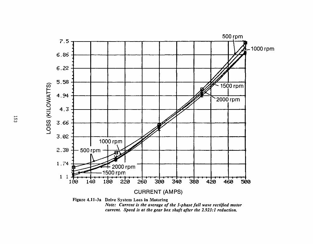
7.5
6.86
6.22
- 5.58 en l-
i 4.94-
0 .....J 4.3
...... ~ -(J1 en w 3.66 en 0 .....J
-. ~ ..... • .!o • " .c.
2.38
1. 74
1 1
500 rpm ~
. ~~
. ~ W ~
~ ~ 1500 rpm 1
~ ~ 1 ..... 2000 rpm
A V
~ V
1000rp, ~ ~ -t- 500 rpm ~17 ~.
~k;:;; ~~. 2000rpm l 1500 rpm : F"""" . . . I •
100 140 180 220 260 300 340 380 420 460 500
CURRENT (AMPS) Figure 4.U-3a Drive System Loss in Motoring
Note: Current is the average of the 3-phase full wave rectified motor current. Speed is at the gear box shaft after the 2.923:1 reduction.
1000 rpm
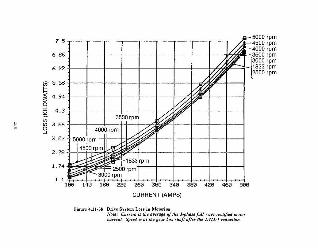
~ U'1 +>0
7 5
r 0-t: •. · ... b
~ 2~· b. c:.
- co coS en .J._. l-I-~ 4.94 0 -1
4.3 ~
~ 3500 rpm -en en "7 --·J.bb 0 l 4000 rpm -1
3.02
? 70 "- . _tv
1-1833 rpm 1 . 74 ~~ 2500 rpm+I---t--I----t---+---+---f
3000 rpm 1 1 f .. , I I I ; I a • I I ••• I I 'Ii . I I 'Ii ; I ••• Ii • • I
100 1413 180 &."='0 260 300 340 380 420 46e 500
CURRENT (AMPS)
Figure 4.11-3b Drive System Loss in Motoring Note: Current is the average of the 3-phase full wave rectified motor current. Speed is at the gear box shaft after the 2.923: 1 reduction.
5000 rpm 4500 rpm 4000 rpm 3500 rpm
{
3000 rpm 1833 rpm 2500 rpm

...... t.T1 t.T1
-en l-
i 0 .....J
~ -en en 0 .....J
5
4.54
4.08
-. .-~
~.o~
3.16
.-, ? Co. I
2.24
1. 78
1.32
.86
.4
\ 500 rpm
1000 rpm
-1500 rpm ~--~--~~--+---~---4----~--4----+--~I~>~4~<~1--2000rpm
2500 rpm
5000 rpm ~4500 rpm
\ 500 rpm
1000 rpm ~ I I I I [~g~~~m I : :
- 4000 rpm
b004 '''" ,2500 rpm
3500 rpm 3000 rpm
10e 140 180 220 260 300 340 380 420 460 C;~3 .... t;.II'_
CURRENT (AMPS)
Figure 4.11-4 Controller Loss in Regenerative Braking Note: Current is the average of the 3-phase full wave rectified motor current. Speed is at the gear box shaft after the 2.923: 1 reduction.
4000 rpm 3500 rpm 3000 rpm
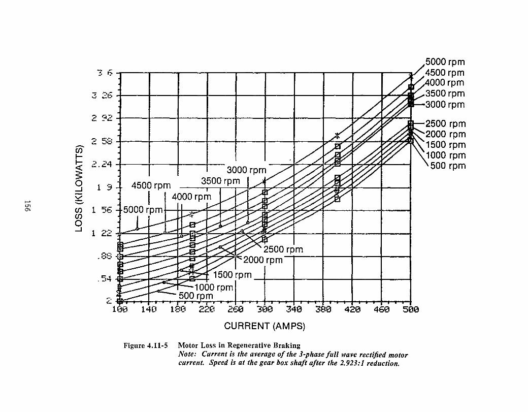
........ (J1 0)
en I-
.... ,. .J ~h.~.-~~--.-.-~~--~---
:3 26 I I 1>< "
~. c.-' c.. _ ~ I >' ,I' j,-';V
,.... r:::::'t-. I ..-:. ..... '0 I L' ./. C ¥ I "S4~4!I > ~kJii'; >
~ 2.24 3000 rpm S
g 1 9 3500 rpm 4500 rpm
~ -en 1 56 5000 )pm I 41100:1d;::~A/'L""'<:;""'7.&-S""",.r;:"""><"'>~<",,~"1:J--_-+-_-+-_--f en o ....J 1 22 .. joe="'"'": ~ I =--.... ==q LA3~:..r ::;oo-<"':.i~~~::"""::/::"'-"+---I----+----t----+
.. 8::: ~ ~......=:: :::J..,........i:»»<'L£>~
. 54 ~ =--""-=::»"'Y".....a== I
2 Iitf=. · I • • I i - ; -; .,' i· . , I • I , a » I I i J » , t J. I I ' »1 i »1 100 140 180 22~1 260 '3013 340 380 420 460 500
CURRENT (AMPS)
Figure 4.11-5 Motor Loss in Regenerative Braking Note: Current is the average of the 3-phase full wave rectified motor current. Speed is at the gear box shaft after the 2.923:1 reduction.
5000 rpm 4500 rpm 4000 rpm 3500 rpm 3000 rpm
2500 rpm 2000 rpm 1500 rpm 1000 rpm 500 rpm
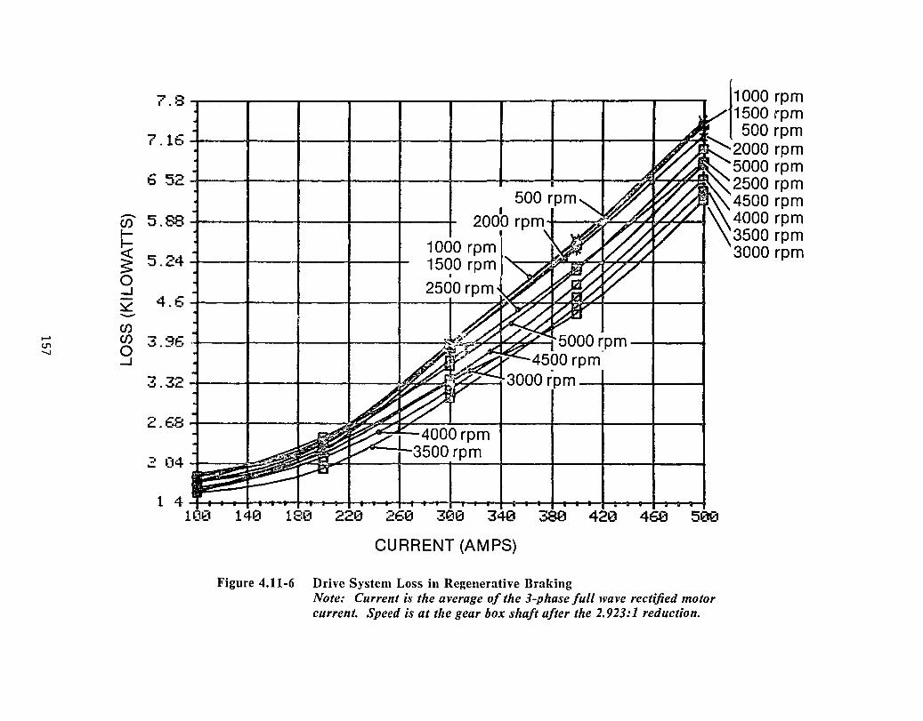
7.8
7.16
6 52
en 5.88 .-.-~ 5.24 0 -l
~ 4.6 -en ...... en 3.96 tTl 0 .......
-l
-; 7.1"\ oJ.oJCo
2.68
2 04
1 4
500 rpm 2000 rpm 4-1---,:t."C~r7'V/"c I
I ~
1000 rpm 1500 rpm
• 2500 rpm
"I ~?7"~ r5000r_pm-t---.... 4500 rpm
-+---+--+---4--~~< ::d:'Y7< .3000 r'pm -+-1 --1----4
1 180 220 340
CURRENT (AMPS)
Figure 4.11-6 Drive System Loss in Regenerative Braking
460 500
Note: Current is the average of the 3-phase full wave rectified motor current. Speed is at tile gear box shaft after the 2.923: 1 reduction.
1000 rpm 1500 rpm 500 rpm
2000 rpm 5000 rpm 2500 rpm 4500 rpm 4000 rpm 3500 rpm 3000 rpm
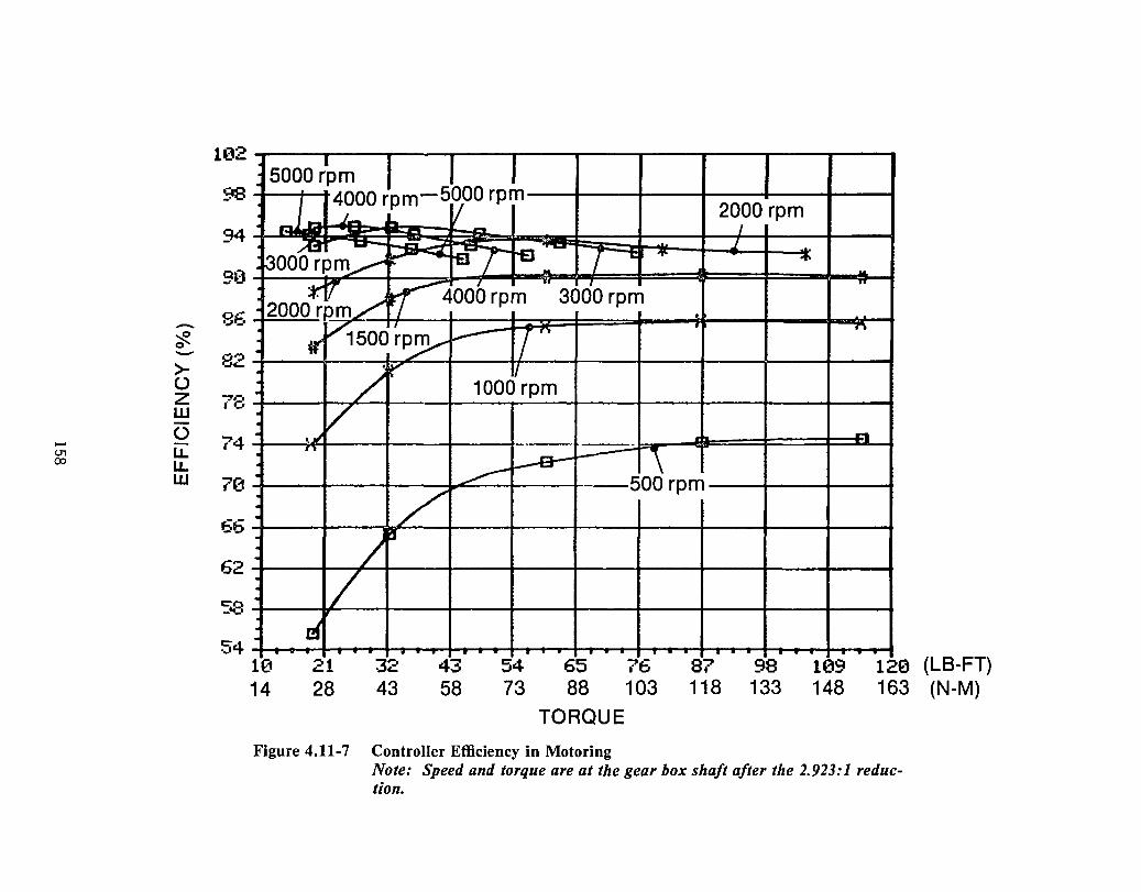
102
98
94
90
- 86 ~ 0 ->-
8":> ~~
0 z 78 w
...... 0 U1
74 00
u.. u.. w 70
66
62
58
54
j 5000 r'pm I -5hoo rpi 2000 rpm
· 4000 rpm ~ J
1. ~ .rw ::::t ~ __ -.-- • "" _~r m - r- I~! l-g ..... 3 - 000 rp!..---"':~., 3000 rpm .. t1T 4000 rpm • ·
· 2000rJ:)mL ~. -;P;50o'r~ ·
.~ !I - - Lf" 1000 rpm · · / I
ul ~~_\ · s. ~ --500 rpm ·
L · · · -
· -
. 1"0 14
L ~
L ~
21 28
-32 43
43 58
. -54 65 76 73 88 103
TORQUE
Figure 4.11-7 Controller Efficiency in Motoring
. 0
87 98 118 133
~ ,--
....... 00
~ .. --
..a
-109 120 (LB-FT) 148 163 (N-M)
Note: Speed and torque are at the gear box shaft after the 2.923:1 reduction.

:?0
85
'=-0 t,;..
75
-:::R 0 70 ->-0 65 Z w 0 60
..... CJ1
LL ~
LL w
55
c;e
4S
40
5000 rpm ...
I I I I
J ~~4000r~m 3000 rpm -2000 rp1m,-; ~ ~1 ~ 1./ ~ - ~/~ ~ -~~
1: ..... - r ~~4000 rp'!l 5000 q~ m - TI" - l~~7 I [3000 rpm 1500 rpm_
#"V 2000 rpm ..l.L • I · -· -
· -r
· -· -· - -. 1'0 14
Lf<' 1~ob rpm
I.
L 1\: -500 rpm
V ~
21 28
L 32 43
. 43 58
. -'- . 54 65 76 73 88 103
TORQUE Figure 4.11-8 Drive System Efficiency in Motoring
--" •
n
-
--~ -
. - . 87 98 109 120 (LB-FT)
118 133 148 163 (N-M)
Note: Speed and torque are at the gear box shaft after the 2.923:1 reduction.
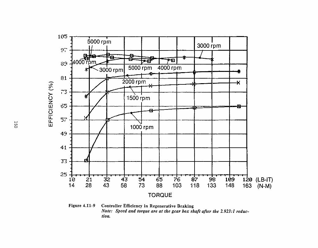
105
Q--- I
89
81 -~ - .... -:1
>- I _.
0 Z W
-t:' t;:.o_1
0
...... LL LL 57
0'\ 0 w
49
41
"7 ..... -,j
'jC" <-J
.! 0 I · 5000 rpm 3000 rpm · I
.... LL- ~ ~ -- J ~ ....
AOO~p ......... t::: - ~ ~ -¥K3000 rpm
·
·
0
·
·
·
Ie 14
.
5000 rpm 4000 rpm ......
...... -.l ••
L I' 2000 rpm . .. . ~ \
t( / • .:" I
1500 rpm
V ~ K~-
J! -'\
L 1000 rpm
I I
~
. . 21 28
32 43
43 58
S4 65 76 73 88 103
TORQUE
.
87 98 118 133
.
... o.
.:J .
_w:::!!.
J J
109 120 (LB-IT) 148 163 (N-M)
Figure 4.11-9 Controller Efficiency in Regenerative Braking Note: Speed and torque are at the gear box shaft after the 2.923:1 reduction.

-~ 0 ->-() Z W ()
..... U. 0\ u. ..... w
105
Q""' -,
89
81
""'7 1·_'
'-E:' 1.: .....
57
49
41
.,-. J ... ..J_
.:.-.:5
4000 rpm 5000 rpm j
~ .."..-P" __ ....
..... · ---· ~ --~ ~ -r ~OOO"pm /" 4000 rpm - 5000 rpm I
~ ->-
30007 2000 rpm · .. . . ~
w / 15(0 rpm
·
·
· 10 14
I :l ~ ~
/ !
~ 21 28
. 32 43
.
"-1000 rpm
4.!. 58
.
-
54 65 76 73 88 103
TORQUE
3000 rpm I
j -.a
"" --'-. <~
---
. . . . 87 98 109 120 (LB-FT) 118 133 148 163 (N-M)
Figure 4.11-10 Drive System Efficiency in Regenerative Braking Note: Speed and torque are at the gear box shaft after the 2.923:1 reduction.

100
90
Be
713
-:::R 60 0 ->-()
50 z w
, •• 'J
~ · ~n ,', ........ .- '''-" "'l
,-,
· I ... - - \ CONTROLLER 10:::1 -.
~~ · £ -1- _ ~FFICIENCY -~
: I j ~ I I
DRIVE SYSTEM
: I r EFFICIENCY ft
J I ..u. SL
~ () 4~3 0\
u. N
U. w
30
20
/ I ., ~- ..
V I \ SPEED · ~
/ ~ /
Ie
1.3
· / V . . . . . . , 10 20 30 40 50 60 70 80 90
TIME (SEC)
Figure 4.11-11 Efficiency over the J227 A-D Driving Cycle
, I~
\ IT! I
i
I (M PH) (KM/H) 50 80.6
40
30
20
I
10
. 0 00
64.5
48.4 ~ m m
32.3 0
16.1
o
4.12 DRIVE SYSTEM PERFORMANCE RECORDINGS
The dynamIc performance of the system In both motonng and regeneratIng was measured. A tYPIcal run (FIgure 4 12-1) IS shown from zero speed to 3200 rpm wIth regeneratIve brakIng back to zero speed The battery voltage IS limited to 130 volts by the controls. This causes some tapenng of the avaIlable brakIng torque at hIgh speed when the battery chargIng current IS high NotIce from Figure 4 12-1 that full torque IS maIntaIned in the constant torque regIOn (0-2200 rpm) and then the torque falls off In the constant horsepower region (above 2200 rpm) The torque response IS rate-lImIted, but IS stIll less than one second. Also notIce that the flux IS constant In the constant torque regIOn and then, when voltage amplItude control IS lost (square wave mode), the flux falls off WIth speed The torque angle and real current respond rapidly WIth little error The stator current falls off slIghtly In motorIng operation and IS low In InItIal regeneratIon because the dc voltage nses as the battery acts as a chargIng capacItor The controller IS stable and has good dynamIc response over the entIre operatIng range Note the torque, IREAL and SINO are zero durIng the 6 second coasting tIme pnor to regeneratIve brakIng
FIgure 4.12-2 IS another run WhICh shows the same signals as Figure 4.12-1, except the dc voltage is on channel 2 Instead of IREAL. This run IS at a higher torque and speed. The battery voltage sags from 110 volts to 100 volts during motoring, rises to 110 volts during coastIng and rIses to 130 volts during regenerative braking. The III reaches 400 amps during motoring, but IS limIted during regenerative brakIng by the controls to protect the batteries.
163

f---4 0'\ -I':>
+t TORQUE 0 (125 LB·INCH/DIV) _ gill i i Iii 1IIIIIIiiiiili i mil 1.1 III ItJ II -r-r
(l~~fi, :tl~lllllllmlllll!jll~ •• I· , ,
~1I-l~iii'lI-!j-Ii!-illlli~I'~S·ICI~I'i-II't~-I~r~I-IIIIIlI-IiIrl-I!~fj-i~r1J.lJl.l!~~ll~tl~~j9 __ -+ t 14+----' f-1 --j SIN 0 0 -H- ,--1
(1 V/DIV) -p ~- G_'.'~ ,~."_,.'"'_:~~ - BRUSH ACCUCHART
(1~~~:'1 J _111.JI'n~-: 'tt (~ elano Orion p r>led n 1I S'"
III +1 r:>'r: (40MDIV) ~, SitE jJ; ::0~ ~ d . ·L
o ,
SPEED (320 RPM/DIV) ~
Figure 4.12-1. Typical Performance Recording

....... Q)
U1
TORQUE (300 LB·INCHIDIV)
DC VOLTAGE (20 VIDIV)
SIN e (2 V/DIV)
IFLUXI (1 VIDIV)
------+ 1-~ r-_____ - -o ~ , _ -_ ~~~_ --=-~-=-~~-; i~-=-2 ~ ___ - -
- - ~ - i- -- - , -
o 1. .• •.•• . .. . ... ~~-_ -~ ~ ----'----..--~L;_-_. c:_~ ~ .~L __ ~ __ ~:;:.--=-__ -=_:...=......::..----:-:-::--::::::==--:-_ -'-_'. ____
+ - 1 sec ~I I..-
+ 1 ~~=-~~-==~~~-~ ~~~~~~ --;) ;#, k-~~--~-----==--~ -~~~ _=i~~~_~~ --~-~ -;~ 9 #~ =-=--=~_ -*, ~ Iii, ; ~:: : ~ I I : i: ;}: , i=;---= - --~~~1~----- ~_--~::_- -__ -- =---- -- ----~E~-: :-+-, ' i:, .RUSH ACCUCHART
,I I I I Ii , '
_L
[ , I ~ ~; f C---'_' _'I_I_'_~~-----:7=.---=--=' f-- r~-----T--+- -~~----
Id~ ~+--L.l~
~~---=t==--
, --I--'-- t I -++ L ~~ 1
t--;j-- t-1
I t+=f-,
--+---+ --, ~,
"-±+ H-r+ t--l-- l ~I-+ -,
" ,
H-l+ 114 I All"
~* §=F- ~I-Ii , J T- , t-f.2='+ t-Ut-, , H-t--
III + 1 (80 AlDIV)
o
'+ 1 --1---Ll- ,-f- ~ ~ ~-H ~~~~-+-- ~ SPEED H+ -:-r-~M ' -r-l , +-;-4+t-~~K _~ --::-" : ;--0 - -
(500 RPM/DIV) + .l~--L +-~ ~~ ~t++--'- r - ;-+
r- LL1_W +--r-'--,-'- L+-t- II I _ I ; --+--1--+-r+--:--- -'--r~ + ~ ~- , ~
o t- ______ ->- ____ ~ .. _ ~ • +------+---_ +- -+-.,. +-----+ _+ ___ ~
Figure 4.12-2. Typical Performance Recording with DC Voltage
Section 5
RESULTS AND CONCLUSIONS
The feaSIbIlIty of a three-phase ac translstonzed Inverter for an electnc vehIcle ac InductIon motor propulsIOn system applIcatIOn has clearly been demonstrated ThIS type of system has potentIal cost and maIntenance advantages over a dc chopper-based system The ac motor has sImple yet rugged constructIOn WIthout commutators and brushes, reqUIres no routme mamtenance, IS amenable to mass productIon, IS capable of hIgh speeds WhICh reduces ItS SIze, and can be totally enclosed allowmg advanced packagIng and coolIng technIques The power mverter In the ac controller utIlIzes the advances In hIgh-power DarlIngton tranSIstors to obViate the need for costly power level commutatIon CIrCUIts that would be needed for a thynstor approach The Inverter IS consequently allowed to operate at hIgher sWItchmg frequenCIes to improve the current waveform delIvered to the motor and thereby mcrease the motor effiCIency The control electrOnIcs In the ac controller utIlIze advances m mIcroelectronIcs to solve the complex control of an ac mverter-InductIon motor dnve system m relatIvely low cost SIgnal electrOnIcs The major results and conclUSIOns drawn from the deSIgn and laboratory test of an Improved ac motor controller SIzed for a battery powered electnc vehicle weIghmg 1633 kg (3600 lb) are
1. The three-phase, ac translstonzed mverter, GE optImIzed mductIOn motor and dnve system control were dynamometer tested In both motonng and regeneratIve brakmg
2. The feaSIbIlIty and Improved motor current waveforms of the advanced pulse WIdth modulation (current-controlled PWM) scheme were demonstrated
3. A famIly of controllers spannmg the range of 10-50 horsepower WIth battery voltages from 84-300 volts were scaled from the base 108-volt, 20 hp deSIgn The baSIC power and control CIrCUIt concepts developed can be applIed throughout thIS famIly WIthout fundamental lImItatIOns
4. The lIfe cycle cost of the ac controller famIly was evaluated and IS less than a dc chopper-based system The hfe cycle cost of the base system was 24¢/km (39¢/mtle).
5 The ac controller losses, motor losses, and total drive system losses were mapped over the current and speed range
6. The efficiency of the ac controller was mapped over the speed and torque range, mcluding the J227a-D cycle The controller and system reached a peak effiCIency of 95% and 86.9%, respectIvely
7. Motor reversing was eaSIly mcorporated mto the dnve system controls by electrically reversing the phase sequence of the mverter.
8. An approach for the utllizatlon of a portIOn of the ac controller power circuitry as a battery charger was presented.
9. The estimated ac controller costs are probably above that reqUIred for the automotIve market. Cost reductIons are clearly pOSSIble from a system redeSIgn that pays speCIal attentIon to system partitIOnmg and pOSSIble performance/cost trade-offs Common parts for various modules would lead to further cost reductlon
10. HIgher horsepower systems need a hIgher battery voltage to reduce costs However, some capaCItor developments are needed at high voltage.
11. The ac controller cost favors a hIgher system voltage than the base 108-volt system The ac controller size and efficiency also favor a higher system voltage because of the resulting lower currents. Most of the Inverter losses are current or current-squared related, such as tranSIstor forward drop and conductor drop, while few are voltage related. The size of the inverter is based on the losses that must be dissipated and the SIze of the components, WhICh
166
are more strongly current related than voltage related Examples are the dc filter capacItors WhIch are sIzed by the npple current requIrements and the number of parallel transIstors whIch are set by the peak currents that must be sWItched
12 The feasIbIlIty of the advanced motor controls usmg the motor torque angle, motor stator real current, and motor flux, wIthout a tachometer, were demonstrated
13 The reasons for the choIce of transIstors for the mverter are well founded, but the mam problems are theIr cost and avaIlabIlIty However, market forces and volume productIon are expected to result m acceptable transIstor pnces and sources m the future
14 The snubber design, transIstor safe-operatmg-area, CIrCUlt layout and system voltage need further development work to reduce the snubber compleXIty and snubber losses (a maJor source of inverter losses)
15 Further development work IS needed to ratIonally evolve a less expensive system control hardware ImplementatIon
16. Further development work IS needed to reduce the base dnve CIrcuIt and base dnve power supply costs and losses. ThIS IS partIcularly Important m the low horsepower range at low battery system voltage
167

Appendix A
ELECTRIC VEHICLE PERFORMANCE ANALYSIS AND SPECIFICATION
1.0 INTRODUCTION
A method of analyzing the performance reqUIrements of an electrIc vehicle is developed. The method uses the basIc pnnciples which charactenze all electncal propulsion systems, regardless of the type of trachon motor used. The result IS a vehicle specIficatIOn from WhICh a detaIled design can be generated.
2.0 ANALYSIS
2.1 PERFORMANCE GOALS
The analysIs denves the vehicle tractIve effort reqUIrements to meet the maximum vehicle performance goals These goals are:
1 AcceleratIOn from 0 to 48 km/h (30 mph) in 9 seconds
2 AcceleratIOn from 40 to 88 km/h (25 to 55 mph) In 18 seconds
3 Sustained speed on a 10% grade of 48 km/h (30 mph)
4. ImtIal acceleratIOn sufficient to start on an 18% grade
5. Mlmmum balancing speed of 97 km/h (60 mph)
The specificatIons above are considered to define the maximum vehicle performance desired and to apply relatIvely Infrequently only once or tWice per battery charge. The balancIng speed IS the speed where the avaIlable dnve power equals the vehIcle fnctIOn and Windage
In additIon to the above specIficatIOns, It IS desIred to operate the vehicle continuously on the 1227a-Schedule D dnvIng cycle ThIS duty cycle Will determine the continUOUS rating of the motor and controller The cycle IS shown In Figure A-I
£ 0-
~ c w w 0-IJ)
CRUISE
50 805 72 4 KM/H (45 MPH) COAST
40 644 ~ ::::644 KM/H (40 MPH)
483 ~/ 30 BRAKE
322 r-ACCELERATION 20 I' 10
o~--~----~----~----~--~~o 20 40 60 80 100
TIME(SEC)
NOTE THE SHAPE OF THE ACCELERATION PORTION OF THE DUTY CYCLE CURVE IS UNDEFINED
Figure A-1 SAE J227a - Schedule D Driving Cycle
169

2.2 FRICTION AND WINDAGE
An equatIOn defimng the fnctIOn and wIndage of the vehIcle IS (4)
608 2 RT = 0.012 W + 0.000029 WV + 391 V
where, RT = total resistance of frictlon and wIndage In lb (1) W = vehicle weIght In lb (3600 lb to be assumed) V = vehicle speed In mph
The first two terms are the vehicle frictIOn and the last term is the vehIcle wIndage The fnction and windage are plotted separately In FIgure A-2 and in total In FIgure A-3.
P 0 U N D S
P 0 U N D S
150
140
130
120
110
100
90
80
70
60
50
40
30
20
10
o
150
140
130
120
110
100
90
80
70
60
50
40
30
20
10
o
o
o
10 161
-t '!-"'
20 322
(681)
(636)
(590)
(545)
(499)
(454) K I
(409) L 0
/p /
FRICTION ~iI' ~
/'
(363) G
(318) R A
(272) M S
(227)
/ "wINDAGE (182)
.,..A ,..........
30 483
SPEED
.....-' r
40 644
50 805
(136)
(91)
(454)
60 70 (MPH) 966 1127 (KM/H)
Figure A-2 Vehicle Friction and Windage
(681)
(636)
(590)
/ /
(545)
(499) )
L (454) K
I (409) L
/" r""
~ l.---"
~
0 (363) G
(318) R A
(272) M S
(227)
(182)
(136)
(91)
(454)
10 20 ~ ~ ~ w ro ~~ (161) (322) (483) (644) (805) (966) (1127) (KM/H)
SPEED
Figure A-3 Total Vehicle Friction and Windage
170

2.3 ACCELERATION
The energy reqUIred for acceleratIOn IS calculated from the formula F = rna, which, translated Into vehIcle terms, becomes
TE = 0.0456 A W + Rotary InertIa Effect
where,
TE = tractIve effort In lb
A = acceleratIon In mph/sec
(2)
The normally expected value of rotary inertia for a self-propelled raIl car will be eqUIvalent to about 9% of the vehIcle weIght In an automobIle drIve, the rotary InertIa may equal or exceed 15% of the vehIcle weIght This analysis assumes that rotary inertia IS 10% of the vehicle weIght, thus
TE = 00502 AW
when rotary InertIa IS Included
The tractive effort can be related to power by the folloWIng equatIOn.
P = 199 TE V
and this power can be related to the motor requIrements by this equation'
P = 0142 nT
where,
P = power in watts
T = torque in Ib-ft
n = motor speed In rpm
2.4 GRADE CLIMBING
RequIrement three IS the abIlity to climb a 10% grade at a continuous speed of 48 km/h (30 mph). Due to the absence of acceleration, the effect of rotary inertia can be neglected. The tractIve effort reqUIred is gIven by.
TE = W sin (tan- l 1~0) where,
G = grade in percent
(3)
(4)
(5)
(6)
The reqUIred tractIve effort IS 163 kg (358 Ib), neglectIng loss. The frIction and windage loss from EquatIOn 1 at 48 km/h (30 mph) is 27 kg (60 Ib), so the total tractIve effort is 190 kg (418 Ib) This point is shown in Figure A-5.
2.5 INITIAL ACCELERATION
Requirement four is the ability to start the vehicle on an 18% grade. The tractive effort required is given by Equation 6, again neglecting rotary inertIa, and is 290 kg (638 Ib). The frictIon from EquatIon 1 at zero speed is 20 kg (43 Ib), so the total tractIve effort needed IS 309 kg (681 Ib). ThIS POInt is shown in Figure A-5.
171

2.6 VEHICLE ACCELERATION MODEL
The first and second reqUlrements deal with the vehicle acceleration between two speeds. In order to analyze these requlfements, a knowledge of the general operatmg charactenstIcs of an induction motor as applied to a vehicle dnve IS reqUlred Figure A-4 shows a vehicle acceleration model which can be used This model does not mclude losses, but losses wIll be accounted for later. Note the three operatmg speed ranges The first (I) IS a constant acceleratIOn region where the motor torque IS constant over the speed range The mduction motor is operatmg at variable frequency and voltage with constant flux (constant volts/hertz) and constant slip The second (II) IS a constant horsepower region where the motor torque falls mversely with speed The motor IS operatmg at vanable frequency with constant voltage and a vanable slip frequency simIlar to field weakenmg, smce the motor flux decreases with speed. VI IS the motonng cornt.r pomt. The third (III) region IS eqUlvalent to senes motor operation, smce the motor IS operatmg at vanable frequency, but both voltage and shp are constant The constant power speed range of the motor IS V2/ VI'
A ACCELERATION
A = Ao V1
~ MOTORING CORNER POINT +---~----------~
CONSTANT ACCELERATION
I CONSTANT
POWER
/ Ao V1 A= -V
II
SERIES MOTOR CHARACTERISTIC
III
Vm
o ~------r-------~-------r-------r-------+-------+----------V SPEED
Figure A-4 Vehicle Acceleration Model
As stated earlier, thiS analysIs approach IS valid regardless of the type of tractIOn motor used ThiS vehicle acceleratIOn model IS apphcable to a dc dnve RegIOn I is basically armature control with constant field as a functIOn of speed RegIOn II IS constant armature voltage with a field current which varies approximately as 10/ V
172

Speed as a functIOn of tIme IS reqUIred m order to convert the vehicle requirements to motor requIrements. The equatIOn
A = dv dt
(7)
IS used for the calculatIOns In speed range 1, A = Ao , thus VI 'I J dv = Ao f dt (8)
° 0
and
(9)
where
VI motonng corner pomt speed, mph
Ao mltIal acceleratIOn, mph/sec
tl tIme to reach speed Vi> sec
Ao VI For speed range II, A = V' thus
V2 '2 f VdV = Ao VI f dt VI 'I
(10)
and
(11)
where V2 = speed at the end of constant power, mph
t2 = tIme at which speed IS V2, sec
VI V2 For speed range III, A = Ao 2' thus
V V J m v2 dv = Ao
v, (12)
and
(13)
where Vm maximum speed, mph
tm tIme at which speed IS Vm , sec
173

2.7 MERGING ACCELERATION
In order to analyze the second reqUlrement, accelerate from 40 to 89 km/h (25 to 55 mph) in 18 seconds, It IS assumed that the entire acceleratIOn IS m the constant power speed range
Assume Vx 40 km/h (25 mph)
~ 89 km/h (55 mph)
ty - tx = 18 seconds
Then, using EquatIOn 11,
V 2 - V 2
Ao VI = 2 ( _ x) = 66 67 ty tx
Ao VI IS a power term and, from EquatIOns 2 and 4 the power over this constant power range, not mcludmg rotary mertIa, IS calculated as follows
p = (1 99) ( 0456) (Ao VI) W = 21,779 watts
(14)
(15)
To account for fnctIon and wmdage, the average value of fnctlOn and wmdage from EquatIon 1 over the 40 to 89 km/h (25 to 55 mph) speed range IS added to the vehicle acceleratIOn power component Thus,
P = 21,779 + 6,634 = 28,413 watts = 38 hp (16)
This sizes the power reqUIred at the wheels of the vehicle as delIvered by the drive system This 38 hp reqUIrement IS plotted 10 Figure A-5 10 terms of tractIve effort versus speed This IS the mmlmum peak horsepower to meet the vehicle acceleratIOn maximum performance requIrement The drIve system must be Sized larger than this to account for rotary mertia effects under acceleratIOn and gear losses
2.8 ACCELERATION - 0 to 48 km/h (0 to 30 mph)
Requirement one IS the abilIty to accelerate from 0 to 48 km/h (0 to 30 mph) m 9 seconds The corner pomt speed VI Will probably be less than 48 km/h (30 mph), so Equations 9 and 11 wIll be used
Assume, Vx = 0 mph
~ = 48 km/h (30 mph)
fy = 9 seconds
Then, usmg EquatIOns 9 and 11,
_ Vy2 + Vf
ty - 2 Ao VI (17)
Since the power term Ao VI can be found from the prevIous acceleratIon reqUIrement, the corner point speed VI can be calculated Thus,
VI = (2 Ao VI ty - V}) 'h = 42 km/h (26 mph) (18)
174
The term Ao Vb mcludmg frIctIOn and wmdage, can be found from applymg Equations 2 and 4 to the power calculated in Equation 16, with the result Ao VI = 86.97
This sets the maximum motonng corner point vehicle speed which relates directly to the base motor speed Above base speed, for maximum tractive effort, the motor operates at constant voltage, fed by the power conditioner operatmg m a square wave mode Below base speed, the motor operates at constant volts/hertz, fed by the power conditIOner operatmg in a pulse Width modulated (PWM) mode This corner pomt speed IS shown in FIgure A-S
2.9 BALANCING SPEED
The fifth requirement IS for a mmlmum balancmg speed of 97 km/h (60 mph). The fnctIon and wmdage of the vehicle from EquatIOn 1 at 97 km/h (60 mph) IS 48 kg OOS lb) The drive system must have this much tractive effort avaIlable to overcome this friction and wmdage This pomt is shown m Figure A-S This reqUIrement could mfluence the choice of speed V2, I.e., the constant horsepower speed range, dependmg on the drive system's capabIlIty of meetmg the balancmg speed tractive effort m Region II or RegIOn III
3.0 REFERENCES
1. L. De KoranYI, "Train Resistance, Power and Energy ReqUIrement of M-U Cars," 9th Joint AS ME-IEEE RaIlroad Conference, May 1966
2. C.T. Hutchmson, "The RelatIOn of Energy and Motor Capacity to Schedule Speed m the Movmg of Trams by ElectrICity," AlEE Proceedings, January 1902.
3 A.B Plunkett and D.L PIette, "Inverter-InductIOn Motor Drive for Transit Cars," IEEE TransactIOns on Industry AppitcatlOns IA-13 0), January/February 1977
4 General ElectrIC Company, "Near-Term ElectrIC Vehicle Phase II Fmal Report," March 28, 1980, DOE Contract No DE-AC03-76CSSI294
S A.B Plunkett and G.B Khman, "Electric Vehicle AC Dnve Development," SAE Paper 800061
700 318
STAAT ON 18% GRADE
600 272 V1 = 42 KMfH (26 MPH) MAX
t 9 SEC 0-48 KMfH ACCELER~.A
(030 MPH) ~
500 227
'" c ... 400 182 a:
~ (;
w ~ > ;:: 300 136 u
'" a: ...
200 91
100 45 97KMfH J (60 MPH)
BALANCING (KM/H) SPEED
16 32 48 84 81 97
10 20 30 40 50 60
SPEED IMPH)
Figure A-5 Summary Vehicle Specifications
175


Appendix B
DESCRIPTION OF INDIVIDUAL CONTROL CARD OPERATION
1.0 INTRODUCTION
The followmg discussIOn IS a detatled descnptlOn of operation for each control card in the control electrolllcs assembly. Each control card refers to ItS schematic drawmg contained in Appendix D. This mformatton supplements the basIc control descnption given m Section 3.6 and can be used for a more thorough understandmg of the controls or for troubleshootmg the mdlvidual control cards Refer to Section 7.0 for the definitions of the conventtons used when discussing signals on the control cards A descnption of the control box used to simulate the conventIOnal automotive dnver commands IS also mcluded.
2.0 DRIVER COMMAND MODULE - EP7644MDCA
The Dnver Command Module is the command control box for the control electronics assembly It simulates the conventIOnal accelerator and brake pedals, forward and reverse, and the Igllltton sWitch It IS attached to the control electrolllcs assembly by an 8-meter (25-foot) cable, enabling the ac controller to be operated from any number of positions, e g , while watchmg another mstrument.
The circUltry consists of two potenttometers buffered by voltage followers, and two toggle sWitches The voltage followers are calibrated to give 0 to + 10 volts for the ACCELERATE· and BRAKE· signal inputs The FORWARD-REVERSE sWitch generates DIRECTION·, which IS a "1" for reverse and a "0" for forward The ON-OFF switch generates ON/OFF*, which is a "1" for on and a "0" for off and also provides a contact closure to pull m the power relay sequencmg circUltry to energize the power inverter.
ThiS box may be replaced by an mterface circUlt which provides two analog signals of 0 to + 10 volts for ACCELERATE· and BRAKE·, two digital signals of 0 or + 15 volts for DIRECTION· and ON/OFF·, and a contact closure to pull in the power contactor sequencing clrcUltry The logiC power supplies (+/-15 volts) are available at the PI connector to power the mterface clrcUltry, but It IS recommended that the clrcUltry be Isolated from the controlhng eqUlpment by IsolatIOn amplifiers for the analog signals and optical couplers or relays for the digital signals The contact closure to energize the power inverter must be a relay contact and may include an emergency shutoff by mstalhng a normally closed contact in series with it.
3.0 CONTROL CARD DESCRIPTIONS
3.1 DRIVER COMMAND AND JERK LIMIT - EP7644CDCA
ThiS card prOVides several functIOns. the mterface from the Driver Command Module to the control electrolllcs, hmltmg of the rate of change of acceleratIOn (jerk), zero-speed shutdown, and automattc reset to prevent "pUllout" (too much angle between the current and flux phasors)
In the Dnver Command interface, ACCELERATE· and BRAKE· are mput buffered, corrected for polanty, and then summed by UUE5 & E6] so that one signal IS obtained. ON/OFF· and DIRECTION· are filtered and buffered by U8[A6]ro produce ION· and FWD·, respectively Several mterlock conditions are applied, the first of which IS that any brake
177

command will overnde any acceleratIOn command BRAKE* > 0 volts IS detected by comparator U4[D6], which sets IBRK to a "0" (U7[05]), which In turn sets NO ACC to a "1" (UlO[C3]). This clamps U1[E6] output to 0 volts by way of UI5[E6], preventing any effect from the ACCELERATE* Input. IBRK = "0" also turns on Q1[OI], which pulls In the brake relay In the power Inverter The second Interlock condition is that If FWD* and FIR (output which IS the actual directIOn) do not agree, NO ACC IS set to a "1" and the ACCELERATE* Input IS Inhibited FIR IS stored In UI4[Bl] and can only be changed If the system IS In a shutdown condition (SDO at UI4[02]) The difference between FIR and FWO* IS detected by U13[CIL This sets FWD*<>F/R = "I" which Inhibits the reset Input to the SDO flip-flop (UI4[D2]) and sets NO ACC = "1"
The combIned ACCELERA TE* and BRAKE* signals are rate hmIted by U2 [E4 & E5] This signal OREAL *) IS proportIOnal to the deSired real current where -10 volts IS equal to full brake and + 10 volts IS equal to full acceleratIOn ThiS CIrCUIt IS scaled to slew from o volts to full scale (+ 1- 10 volts) In approximately 1 second In additIOn, two clamps are apphed to the signal The first IS UI5[E4], WhIch wIll Instantly force any posItIve output to o volts In response to the NO ACC signal ThiS prevents a posItive (acceleratIOn) command for IREAL * whIle allOWIng a negatIve (brake) command The second IS U 15 [E4], which clamps both polantIes of the output to 0 volts at Jerk hmlt rate In response to the RESET signal RESET IS caused by either ISO (from EP7644CPRA) or IFLUXI< MIN (U7 [C5])
Zero-speed shutdown (SOO) IS generated by flIp-flop UI4[02] In response to one of three sources The first IS In response to ON/OFF* through U8[A5], UI2[B3], and Ull [C2] and occurs Immediately The second IS the power-up reset functIOn (P U RESET) at U8[B3], which forces the system to a reset condition at power-up The third condition IS the actual zero-speed shutdown sequence The sequence IS Initiated when speed (FREQ*) becomes less than a threshold set by R26 and 27[C6], which trIPS comparator U5[C6], generatIng S< 2 [mph] S< 2, In either coast or brake modes, Will generate SO REQ (shutdown request) at UlO[C3] ThiS clamps IREAL * (U15 [E5]) to 0 at Jerk-hmlt rate, caUSIng a smooth reductIOn of torque. When IREAL* reaches 0 volts, WIndow comparator U6[B6] IS tnpped generatIng IREAL * = 0 at U9 [B5] When both conditIOns eXIst, the sequence IS complete and the SDO flip-flop IS set Once SOO has been set for any of the above reasons, It can only be released If ON/OFF IS set for turn-on, power-up reset has timed out, and the ACCELERATE'" Input IS > 0 volts (and not over-ndden by BRAKE"')
IFLUXI< MIN IS generated when IFLUXI becomes less posItIve than a mInimum threshold set by R32[C7] and R33[C6], and tnps comparator U5[C6] ThiS conditIon occurs when the angle of apphed voltage exceeds the pullout angle of the motor and the motor flux collapses The resultIng clamp of IREAL * to 0 volts removes the applIed torque from the motor usually fast enough to prevent pullout As soon as the rotor flux bUIlds up, RESET IS removed and IREAL * ramps back to the ongInal level
3.2 Current Transducer Interface - EP7644CTIA
The current transducer Interface card proVides two functIOns the cahbrated reference biaS sources for the Hall effect current transducers, and the differential amphfiers for readout of the transducers The reference source consists of a 5-volt regulator and tnmmed resistors In senes with the transducers' biaS current Input. The current sources are tnmmed SInce the output of the transducers have a direct (I 1) sensItivity to the bias current The transducers' output Signal IS very low (50 mV = 1000 amps), supenmposed on a hIgh common mode signal (approximately two volts), requlflng a high gaIn preCISIOn amphfier to achieve a useable Signal The outputs of the card are scaled to 100 amps/volt (10 volts = 1000 amps), which
178
requires a gaIn of 200. To mInImIZe the effect of high Impedance resIstors on the offset voltage, aT-network was used for the feedback resIstor. In addItIOn, the two Input dIvIders for each op amp were tnmmed to mInImIZe the effects of resIstor tolerances on the common mode rejectIOn ratio (CMRR) of the amplIfier cirCUIt
The calIbratIOn of the card proceeds as follows
1 The bIas current IS set by selectIng the tnm reSIstor RS1 (RS2,RS3) whIle mOnItoring the bIas current to the transducer ThIS must be done for the specIfic transducer In use SInce the bIaS current requlfements for cahbrated operatIon, as well as the Internal Impedances vary from transducer to transducer Once the bIas cIrCUIts have been calIbrated, the transducer must not be replaced WIthout re-cahbratIng the CIrCUIt
2 The output amplIfier IS set by selectIng two reSIstors, RS4 (RS5,RS6) and RS7 (RS8,RS9), one In the non-InvertIng Input network and one In the invertIng Input network, WhICh IS part of the feedback The two reSIstor selectIOns are Interactive, so that several Iterations WIth decade boxes or pots are requlfed RS4 (RS5,RS6) has a greater effect on the CMRR but some effect on gaIn, and RS7 (RS8,RS9) has a greater effect on gaIn but some effect on CMRR A current source IS reqUIred which can be accurately set and vaned from 0 amps to several hundred amps FlfSt, set the current source to o amps and adjust RS4 (RS5,RS6) for 0 volts on the output Next, set the current source to the calibration point, 400 amps, and set RS7 (RS8,RS9) for 4 volts on the output Repeat these steps until both condItions are satIsfied at the same time (A convenIent test source can be achieved USIng 50-conductor nbbon cable and connectors so that 50 turns can be Inserted through the transducer and qUIckly connected In senes Then 8 amps times 50 turns or 4 amps times 100 turns IS eqUIvalent to 400 amps)
3.3 TORQUE CARD - EP7644CTQA
The torque card contaInS three major functions the flux coIl Input Integrators, the current transformer Input amplIfiers, IncludIng the hlgh- and low-pass filters and transducer Signal summIng amplIfiers, and the vector cross-product calculation of motor torque.
The flux coIl Input Integrators are low offset preCISIOn amplIfiers to minImIZe the effect of offset voltages due to the Inherent high gaIn of an Integrator The Integrators are calIbrated by a senes resistor In the Input network Thelf outputs are the flux phasor (FL UXA,FL UXB,FL UXC)
The current transformer Input CirCUIts [A4] conSIst of precIsion 50-ohm burden resistors for the 4000-turn torOidal transformers, YieldIng an 80-amps/volt scale factor The three resultmg Signals (IA2,IB2,IC2) are high-pass filtered at 400 Hz by C22 (C23,C24) and R48 (R49,R50). The transducer Interface outputs (IA1,IB1,ICl) are high-pass filtered at 400 Hz by R45 (R46,R47), R67 (R68,R69), and C25 (C26,C27). The two sets of Signals are then summed by UlO[B4] (UlO[A41,Ull [A4]) to produce the compOSIte total current phasor (IA,IB,IC) .
The vector cross-product calculatIOn IS done by first convertIng the three-phase current and flux Signals (IA,IB,IC and FLUXA,FLUXB,FLUXC) to two-phase (d-q) eqUIvalents as follows
Id = IA
Iq = IC-IB .J3
179

FLUXd = FLUXA
FLUX = FLUXC-FLUXB q .J3
The two-phase equivalents are then multiplIed and summed to produce
(FLUXq x Id)-(FLUXd x Iq) ~ [FLUX~LUXB x IA]- [FLUXA x I~B] The multIplIcatIOns are done by U7[D3] and U8[C3] and summatIon IS done by U6[DS]
The result IS then filtered by U6[D6] The four JFET transistors (QI-Q4[D4 and C4]) are dnven in pairs by Q I and Q2 [ES] In response to FIR * This IS to reverse polanty of the torque signal (T) when In reverse so that pOSItive values of torque correspond to acceleratIOn and negatIve values correspond to brake, regardless of duectIon
3.4 CURRENT LIMIT - EP7644CCLA
The maJonty of this card IS nonfunctIOnal, beIng left over from early stages In the development of the system. The ongInal use was to detect currents In excess of a maximum allowable value and to force the power Inverter to sWitch by way of overndIng Inputs to the lockout card. This IS now unnecessary, due to the technIque of controlhng current directly In the tightest Inner loop of the controller Current lImit IS Inherent In this technIque
The portion of the card which IS still used IS the generatIon of total current magnItude (III) for use by the angle regulator The dIOdes around UIOA and UIOB [D4] form a three-phase full-wave preCISIOn rectifier YieldIng an unfiltered full-wave rectIfied dc signal.
3.5 FLUX CONTROL - EP7644CFCA
This card has two maIn purposes to generate the IFLUXI feedback Signal for the angle re-' gulator, and to control the amplItude of the Inverter output by way of the amplItude control Input Qlr> to the SIne-wave reference generator
The flux phasor signals (FLUXA,FLUXB,FLUXC) are full-wave rectified by ICIA, ICIB, and IC2B and then summed by IC2A and filtered by IC3A to generate the feedback Signal IFLUX~
The reference for the flux regulator QFLUXr) IS set by R2S/RS9 and IC4B[C4] when IREAL * = 0 volts This IS the eXCitation level for the motor when no torque IS beIng generated, and IS set to reduce battery draIn at coast condltIons.IFLUXr IS compared to IFLUXI by IC4A[C21, which generates Ilr, the current amplItude command IREAL* is rectIfied by ICSA[D2] and added to IFLUXr at IC4B[C4] to Increase the current when the motor IS supplying torque. The maximum value of IFLUXr is set by RS8/RS7[DS] clamp. When IREAL * is Increased abruptly, the flux regulator cannot respond Immediately and a momentary decrease In flux would result were It not for an additional input (dIFLUXI) to the regulator which IS proportional to the rate of change ofiIREAL*1 and causes an immediate boost in Ilr AdditIonal clamps are applIed to the flux regulator output by R24/R36B (minimum) and R30/R29 (maximum). These prevent the total effect of the Inputs to the flux regulator from exceeding the minImum and maximum flux levels of the motor.
NOTE: The latter is extremely important since it defines the ultimate current limit POInt of the current controller. This limit can be set lower (and, indeed, it should be) when first energizing the system after any changes have been made This IS easIly accomplished by connecting a resistor in parallel With R29. With R29 = I S kIlohms, the maximum peak current value is 600 amps. This IS a safe operatIng POInt for the power Inverter containing General
180
ElectrIc power modules, but should be reduced to 450 amps when usmg Power Tech power modules by parallelIng R29 wIth a 24 kIlohm resIstor.
3.6 ANGLE REGULATOR - EP7644CARA
The angle regulator IS the most complex card m the system and con tams several functIOns: the real current OREAL) calculatIOn, the real current controller, the angle (SIN 0) calculatIon, the angle controller, the tractIon battery under-voltage and over-voltage lImits, the derIvative of ISIN 0* I calculatIOn for flux regulator boost, and shutdown and reset overndes to the frequency control output
The feedback Signal IREAL IS calculated from torque (T), flux (IFLVXI), and current (lID usmg a preClSlon analog diVider (V7[C7])
T IREAL = IFLVXI- 014111
ThiS IS filtered by VII [E5] and presented to the IREAL controller V3 [C6] Here, it IS compared to IREAL * from VI [C7] and the error SIgnal SIN 0* IS generated.
The under-voltage and over-voltage hmlts are Imposed on SIN 0* at V4[C5] The traction battery voltage IS sampled differentially on the power mverter and mput to differential amplifier VI [E7] The majorIty of the mput resistances (190 kIlohms) are on the power mverter, which hmlts the value of voltage enterIng the control electrOnIcs to a low value. The output of VI IS scaled at 20 volts/volt and IS processed by two high-gam lImit amplIfiers These overnde SIN 0* at values predetermined by PI and P2 potentIOmeters PI sets the overvoltage hmlt and IS presently set at 135 volts ThiS lImits the maximum voltage that the batteries will be charged to dUrIng high speed brakmg. P2 sets the under-voltage lImit and determmes the lowest that the mverter can draw the batterIes dUrIng acceleratIOn, and is presently set at 75 volts Both of these lImits act to reduce power levels in a lInear fashIOn rather than shuttmg the mverter down A shutdown functIOn eXists on the protectIon card and Will be discussed m that section Clamps are applIed to SIN 0 (R66/R64 and R67/R65) to lImit the maximum slIp angle that can be commanded to mmlmlze pull-out of the motor.
The SIN () feedback signal IS calculated from IREAL and III usmg another precIsion dIvider (V8[C6]).
IREAL SIN () = 0016111
SIN 0*, after voltage limits are applIed, IS compared with SIN () by mtegrator V5[DI]. The error generated IS FREQ* and, controls the frequency of the sme-wave reference generator.
When flux falls below the minImum threshold defined on the driver command card, which may happen If the motor 'pulls out' due to excessive angle or a load torque surge, the reset Signal Will cause IREAL * to be clamped to zero. It will also clamp SIN 0* to zero through QI[D4] and momentarIly clamp the angle regulator integrator to zero through C13, R75, and VIO[E2]. The mtegrator wdl be released when C13 discharges and Will mtegrate back toward synchronous speed at which time the flux Will buIld back up m the motor and reset wIll be released.
When the mverter IS commanded to shutdown (SD), the angle regulator is clamped to zero to reset the mtegrator to zero frequency. When SD is released, the integrator Will integrate toward posItive frequency If the motor is at a stand-still, the flux Will build in the motor Immediately and the drIver command card wIll release IREAL *, resultmg in motor torque. If the motor IS turnmg, the frequency will mtegrate upward untIl synchronous speed
181

IS reached, at which tIme flux wIll buIld In the motor as before.
The remaIning functIOn on the card calculates the denvatIve of SIN 0* for boostIng the flux regulator SIN 0* IS precIsion rectIfied by UI2 [C3] and then differentIated by U13 [B2] A clamp is applied (U13[BI]) to hmit the amount of boost to a moderate level dunng an Increase In ISIN 0*1 and to a very small amount dunng a decrease in ISIN O*~
A final feature of the card is U4[C21, the driver for the SD LED on the front panel. This LED is a two-color device which IS red when the controller IS shut down and green when SD is released
3.7 PROTECTION AND CURRENT CONTROL - EP7644CPRA
This card contains two major functIons' system mOnItorIng for automatIc shutdown protectIOn, and the current control loop comparators
Shutdown (SD) IS initIated In response to anyone of eight possible fault conditIons' tractIOn battery over-voltage, tractIon battery under-voltage, + IS volt under-voltage, -IS volt under-voltage, Interlock fault, heatsink over-temperature, zero-speed shutdown, and a spare Input
TractIOn battery over-voltage and under-voltage conditIons are sensed by monitonng dc volts/20, whIch IS the 20 volts/volt scalIng of the tractIOn battery from the angle regulator card. This Signal IS compared to thresholds scaled by RlS/R17 for the over-voltage case and RI6/RI8 for the under-voltage case. When these thresholds are exceeded, the appropnate comparator trips (U2[B6]) and sets SD at U6[C4]. A latchIng LED wIll also be tripped (LED2[D2]) and wIll remain tnpped by way of SCR2[D31, even If the fault conditIon no longer eXists ThiS wIll remaIn to annunCiate the cause of an unexpected shutdown as long as +/- IS-volt power remains vahd, or the LED may be reset by preSSIng a button on the front edge of the card
The +/- IS-volt power supphes are monitored by the clfcUltry associated with U1[DS & D6]. If the + IS-volt supply sagged, for example, the voltage at the JunctIOn of RS/R6 would become negative and tnp the upper comparator SImdarly, the -IS-volt supply would effect the voltage at R 7/R8 and tnp the lower comparator If both supphes sagged together, the zener diodes (ZDlIZD2) would remaIn biased long enough to ensure that both comparators would trip. Additional capacitors CS/C6 are diode decoupled from the maIn filter to ensure the protectIOn circuitry has tIme to set the SD Signal and stop pulses from reachIng the power Inverter durIng the loss of control logiC power ThiS fault also sets a latchIng LED to annunCiate the cause of an unexpected shutdown In the case where the supphes only sag In voltage rather than shut off completely
The interlock fault detector checks for a continuous electncal path from the INTERLOCK input on the ProtectIon card to common on the Transducer Interface card. The path uses different PIn combinations on each card so that each card must be plugged Into the correct slot to allow operation. Interlock faults wIll latch an LED
HeatsInk over-temperature wIll open one of two temperature senSIng SWitches on the power Inverter caUSIng a shutdown command The SWitches are located on the two heatsInks furthest from the fans since these wIll normally run the hottest The SWitches are connected In senes so that either wdllnItlate a shutdown If too hot. There IS an extra contact Wifed In senes With the heatsInk over-temperature switches, which IS not related to the over-temp function directly. An auxlhary contact on the power contactor IS used to hold the Inverter shut down untd the contactor has closed ThiS prevents the Inverter from turnIng on the power Inverter whIle the senes-chargIng resistor IS chargIng the mam capacitors The result If
182

this were not mcluded IS that the power mverter wIll dIscharge the capacItors faster than the resIstor WIll charge them, leavmg the resIstor as the total load across the tractIOn battery, a sItuatIon that the resIstor IS not sIzed to accept for more than a few seconds' The result of addmg thIS contact IS that the heatsmk over-temp LED wIll always be tnpped and latched before the power mverter IS energIzed If It IS deSIred that the LED correctly annunCIate an over-temp shutdown, the ProtectIOn card must be manually reset after the power contactor IS energIzed
Zero-speed shutdown (SDO) IS generated on the Dnver Command card as dIscussed m that section ThIs shutdown mput does not have a latchmg LED annunCIator smce It IS the normal mode of controllIng the shutdown of the mverter
The spare mput IS Identical m nature to the SDO mput and IS normally grounded to allow operatIOn of the mverter It could be used as a shutdown mput If a normally closed (open = SD) contact were to be mstalled m place of the present Jumper to common.
3.8 LOCKOUT AND WAVEFORM GENERATOR - EP7644CLOA
The Lockout and Waveform Generator card contams two major functIOns the sme-wave reference generator, and the lockout functIOn
The sme-wave reference generator synthesIzes three smusoidal waveforms separated by 120 electncal degrees, whose amplItude IS controlled by II~ and whose frequency IS controlled by FREQ* The reference generator conSIsts pnmanly of a microprocessor (U18[D3]), three digital- to-analog (DI A) converters (U 19 [D2] ,U20 [C2], U21[B2]), and a voltage-to-frequency (V IF) converter (Ul7[B5]) The mIcroprocessor computes the relative amplItudes of the three waveforms at a smgle pomt m the penod and sends the results to three DI A converters The amplItude of the waveforms IS controlled by an analog voltage SIgnal (/I~), WhICh IS generated by the flux control loop ThIS SIgnal enters the card on C12 and IS mverted to form two reference voltages (+ VREF & - VREF), whIch are then sent to the three multIplymg DI A converters The dIgItal mput sets the pomt on the waveform and the analog mputs ( + VREF and - VREF) are the multIplymg scale factor FREQ* (the frequency control SIgnal) IS converted by the V IF converter to a pulse tram whose frequency IS proportIonal to the deSIred frequency of the waveforms ThIS pulse tram clocks the reference generator, causmg It to compute succeSSIve sets of values of the waveforms The result IS three smusoidal waveforms WIth dIscrete "staircase" values whIch then must be filtered (on the protectIOn and current control card) FIR * IS used as a dIrect mput to the mIcroprocessor and determmes whether the next pomt calculated IS the succeedmg or precedmg pomt m the look-up table m the mIcroprocessor's memory U15[D6] and U16[C6] generate clock SIgnals used by the lockout sectIOn
The lockout sectIOn of the card splIts the phase command SIgnals (IA COMM, IB COMM, IC COMM) mto separate upper and lower power module drIve commands (AU, AL, BU, BL, CU, CL) to WhICh a lockout function IS applIed to force a penod of tIme between one power module's turn-off and the complementary power module's turn-on. ThIS prevents overlap of the power modules' conduction hmes to prevent a "shoot-thru," a condition WhICh would occur if a continuous path eXIsted through both power modules m the same phase, causmg a hIgh-fault current WhICh would destroy the two power modules mvolved The card first denves a clock pulse from both flsmg and fallIng edges of IA COMM (IB COMM, IC COMM) by clockmg the waveform through flIp-flops U1 (U6,U10). The flIp-flops are dIfferent for one clock tIme as the waveform rIpples through and generates a pulse through exclUSIve-or gate U2[D6] (U2[C6], U2[B6]) ThIS trIggers one-shot U3[D5] (U9[C51, U3 [B5]) to generate the lock-out pulse The lock-out pulse delays settmg the lower module flIp-flop U5[D3] (U8[C3], U12[B3]) until after the upper module flIp-flop U5[E3] (U8[D3],
183

U12[C3]) has been reset and vice versa The upper and lower module flip-flops are buffered out of the system by hne dnvers conSisting of transistors QI/Q2 (Q5IQ6, Q9/QI0) and Q3/Q4 (Q7/Q8, QIl1Q12). These buffers dnve the base driver modules (EP7644MBDA) on the power Inverter assembly through coaxial cables The base dnver modules are optically coupled at the input, and are designed to source base current to the power modules when current IS floWIng a, the Input, and to SInk base current from the power modules when Input current IS not flowir:g The current SInk mode of operation IS Intended to "sweep out" stored charge from the base Junctions of the power modules for fast turn-off
184
Appendix C
SETUP INSTRUCTIONS FOR AC CONTROLLER OPERATION
1.0 INTRODUCTION
A great deal of care IS required dunng the Initial setup of the ac controller Once the system IS correctly Installed, it IS highly tolerant of "operator errors," but errors In the inItial setup phase can cause eqUIpment damage.
The tractIOn battery bank must consist of senes-connected battery UnIts totallIng 108 volts (e.g, 18 UnIts at 6 volts/UnIt) havIng sufficient capacity to supply 450 amperes without signIficant voltage loss due to IR drops. The 108-volt posItive lead is connected to the 450-amp fuse mounted on the power contactor on the power Inverter, and the 108-volt common return IS connected to the longer bus bar Immediately adjacent to the 450-amp fuse. It IS recommended that a contactor or other means of disconnectIng the traction battery from the power leads at the source end as well as additIOnal fusing be proVIded for safety reasons
The l2-volt aUXIlIary battery must be connected to the ac controller at the power Inverter through cables sufficient to carry 20 amps dc steady-state + 12 volts to TB2-l and 12 COM to TB2-2. The power inverter and the control electronIcs are interconnected USIng the multiple tWisted-pair cable as follows (1) the red and black paIr IS connected: red to TB2-l and black to TB2-2 on the power Inverter, and red to TBl-7 and black to TBl-8 on the control electronICS umt (thIS applies the aUXIlIary battery to the power inverter first where most of the current IS drawn, and to the control electronIcs second), (2) the whIte and black paIr is connected' white to TB6-2 and black to TB6-l on the power inverter, and white to TBl-l and black to TBl-2 on the control electronIcs UnIt ThIS connects the tractIOn battery voltage feedback.
NOTE: The tractIOn battery should be Isolated from earth ground and the l2-volt auxiliary battery connected to earth ground at the chassis of the control electronIcs unit. This will result in the least inCIdence of ground loops and WIll aVOId high fault currents from the traction battery should a connectIon be made Inadvertantly between the traction battery power CIrCUIt and any point in the control electronics circuitry
The remaInIng connectIOns to the control electronics are straIght-forward through cable connectors WhICh are keyed so that they can only be connected to one socket. These Include: P3 - current transducers, Pll - current transformers, P4 - relay control to the power Inverter, P2 - flux coIls In the motor, PI - dnver command module (or custom interface), and P5-PIO - the coaXial cables to the base driver modules on the power Inverter.
NOTE. The connections for the current transformers have not been Implemented on the second control electronics assembly (reSIdual inventory). If thIS assembly is used, the reqUIred CT's must be connected Into the Torque card as shown on EP7644MCEA and EP7644CTQA
The motor connectIOns are made USIng the Motor TermInal Board draWIng -EP7644MMTA. It IS Important that the motor current leads and the flux coIl voltage leads agree as to correct phase rotation or the torque, real current, and angle calculations will all be Incorrect If the motor accelerates In one direction and brakes in the other when no acceleration or brakIng torque IS being called for, the probable cause is that only one set of flux cods
185

IS connected. ThIs wIll cause the flux vector to be rotated by IS-degrees WhICh creates a IS-degree error m the angle calculatIon
2.0 INITIAL POWER APPLICATION
When power IS first applIed, several steps should be taken to verify that correct voltages and polan tIes are applIed and that connectIons have been properly made These should first be checked vIsually and then at low voltage and current levels The followmg procedure IS recommended as a step-by-step approach to thIS venficatIon procedure
VIsual check
1. Verify that all connectIons on the power mverter are correct and tight This IS partIcularly Important for the bus bar connectIOns between half-phase modules and the bus bar connectIOns at the dc filter capaCItor bank Also make certam that the small L-shaped bus bar from the power module to C2 IS m place ThIS pIece IS easIly omItted, e g , If power modules have been changed If so, the OppOSIte power module WIll turn on once but WIll be destroyed at the first turn off due to over-voltage smce the free-wheelmg dIode WhICh protects a gIven power module during turn off IS in the OppOSIte power module
Low voltage and current checks'
2 Temporanly dIsconnect the tractIOn battery supply, dIsconnect PI (dnver command module) and pull all of the electrOnIc cards out at least one mch to dIsconnect them from the power supplIes DIsconnect the 12-volt power at each base dnve module (square black plug) If pOSSIble, replace (temporanly) the I2-volt auxIliary battery WIth a power supply capable of 12 volts and 20 amps mmlmum Turn on the 12-volt auxIlIary battery supply and venfy that less than 1 amp of current IS bemg drawn Venfy that the +/- IS-volt dc/dc converters are functIOnmg by measunng from PI-G to PI-J and from PI-H to PI-J Turn off the aUXIlIary battery supply
3 Plug m the electrOnIc cards and connect PI Connect the 12-volt power at each base dnve module WIth the ON/OFF SWItch on the dnver command module m the OFF pOSItIon, agam turn on the aUXIlIary battery supply Venfy that approXImately 5 amps (+/- 1) are flowmg WIth a DVM or multImeter, measure each base dnve module from B2-to-E and from BI-to-E at the output termmal board B2-to-E should measure -3 (+/- 1) volts and BI-to-E should measure -4 (+/- 1) volts WIth approxImately 1 volt dIfference between them ThIS mdlcates that all base dnvers are recelvmg turn off commands (negatIve voltage) and that the power modules do not have shorted base Junctions (voltages greater than 1 volt m magnItude)
4 WIth the tractIOn battery stIll dIsconnected, place the ON/OFF SWItch on the dnver command module m the ON pOSItIon The power contactor should pull m Immediately and the aUXIlIary battery supply current should mcrease tu approXImately 10 (+/- 1) amps Place the ON/OFF SWItch m the OFF pOSItIon and turn off the aUXIlIary battery supply
5. Pull out the protectIOn card and connect a Jumper from + 15 volts (card pm 32) to the end of R23 nearest to U9 to defeat the tractIOn battery under-voltage functIOn Replace the protectIOn card, turn on the aUXIlIary battery supply, and venfy that the supply current IS approXImately 5 amps WIth both ACCELERATE and BRAKE controls fully counterclockWIse, place the ON/OFF SWitch m the ON posItIon The contactor should agam pull m and the current should nse to approXimately 10 amps Turn the ACCELERATE control partIally clockWIse and observe the LED mdicator on the front cov-
186

er change from red to green The current should nse to approxImately 15 amps (+/- 2) This mdicates the base dnvers are sourcmg current into the power modules. Turn the ACCELERATE control fully counterclockwise, the ON/OFF sWItch to OFF, and turn off the auxIhary battery supply.
6. Connect an oscIlloscope dIfferentially across Bl-to-E on A-upper base dnve module and Bl-to-E on A-lower base dnve module (two dIfferential mput pairs). Turn the auxIliary battery supply on and observe that the oscIlloscope shows two dc sIgnals at approxImately -4 volts. Place the ON/OFF switch to ON, turn the ACCELERATE control clockWIse, and observe two square waves appear and smoothly increase m frequency. The waveforms should sWItch between approximately -4 volts and + 1.5 volts When the waveforms reach maximum frequency, expand the oscilloscope time base and observe that the two waveforms are of OpposIte phase and each slightly less than 50% duty cycle The fallIng edge of each must occur 25 microseconds (40 for Power Tech power modules) before the nsmg edge of the other to prevent overlap and resultmg "shootthru" (see sectIOn on lockout card). Repeat for B-upper and B-Iower and for C-upper and C-Iower
7 Reconfigure the OSCilloscope for three-channel, smgle-ended operation and observe Bl-to-E on A-lower, B-Iower, and C-Iower These should appear as three waveforms at 120 degrees phase shift from each other
8. Usmg a dc current probe, observe the Bl and B2 base currents of each power module (close probe around Bl and B2 wires together) The current should have a rise-time of less than 1 microsecond to a level of approximately 4 amps and a fall-time of less than 1 microsecond to a narrow negative pulse of approximately - 5 amps followed by a level of -05 to -1 amp The negative pulse IS the "sweep-out" of current from the baseemitter Junction forcmg rapid turn off of the power module Turn the ACCELERATE control fully counter-clockwise, the ON/OFF SWitch to OFF, and the auxIliary battery supply off
9 If all of the above tests have been successful, the power mverter is now ready to apply power to the motor It is advlseable to do thiS at very low currents and voltages however, to venfy that the control electrOnIcs are fully functional. To do thiS, connect a power supply capable of 20-40 volts and 20-50 amps m place of the traction battery. Connect three OSCilloscope channels to lA, IB, IC on the torque card (EP7644CTQA) and a fourth to IA COMM on the protectIOn and current control card (EP7644CPRA) WIth the higher current supply off, turn on the aUXIlIary battery supply, place the ON/OFF SWitch ON, and turn the ACCELERATE control fully clockWise as m step (6) above When the waveform on IA COMD reaches maximum frequency, slowly bnng the high current supply up whIle watchmg lA, IB, IC. A set of three smusOidal waveforms should appear at the same frequency as IA COMD and at 120 degrees phase shift from each other These should grow m amplItude as the high current supply IS increased Turn the high current supply off, the ACCELERATE control fully counterclockWIse, the ON/OFF SWitch OFF, and the auxlhary battery supply off.
Full voltage and current checks.
10 The power mverter IS now ready for normal operation Pull the protection card, remove the Jumper so that the tractIOn battery under-voltage IS functIOnal, and replace the card. Remove the flux control card (EP7644CFCA) and connect a 7 5 kohm resistor in parallel With R29 to reduce the current hmlt Replace the auxIliary battery supply With the aUXIlIary battery, and the high current supply With the tractIOn battery and close the appropnate breakers Connect a multImeter across the dc filter capacitor bank or monitor
187

- DCV /20 on the angle regulator card Make sure that the ACCELERATE contraIls fully counterclockwIse, then place the ON/OFF sWItch to ON and thIS tIme the contactor on the power inverter should not close Immedtately Instead, the capacitors will charge up, takIng two or three seconds, then the contactor wIll close and the blowers should start Turn the BRAKE control shghtly clockwIse and verIfy the blowers drop In speed IndIcatIng the system IS In brake Return the BRAKE control fully counterclockwIse, then turn the ACCELERATE control slowly clockwIse The power Inverter should start and the motor should begIn to accelerate at a slow rate MOVIng the ACCELERATE control fully counterclockwIse should put the system In coast or, if InSUfficIent speed has been developed, WIll shut the system down If sufficIent speed has been developed to remaIn In coast wIth the Inverter runnIng, turn the BRAKE control slowly clockwIse and observe the motor slOWIng down. As brake rate IS Increased, observe also, a rise In the tractIOn battery voltage IndIcatIng regeneratIOn Into the batterIes Power down the system, and remove the 7 5-kohm resIstor from the flux control card to regain full current limit
The system has now been fully checked out In a step-by-step procedure WhICh should avoid damage, If any errors occurred In settIng up The eqUIpment can therefore be pronounced fully operatIOnal.
188

Appendix D
AC CONTROLLER DRAWINGS
ThIS appendIx contaInS the folloWIng drawings for the power Inverter and control electronICS of the ac controller
• EP7644MIVA, Power Inverter, SchematIc and Assembly, 2 sheets
• EP7644MPHA, Half Phase Module, SchematIc and Assembly, 1 sheet.
• EP7644CBDA, Base DrIve, SchematIc, 1 sheet
• EP7644SICA, System InterconnectIOn, DIagram, 1 sheet.
• EP7644MCEA, Control ElectrOnIcs, Schematic and Assembly, 2 sheets.
o EP7644MDCA, DrIver Command Module, Schematic and Assembly, 1 sheet
o EP7644CARA, Angle Regulator, Schematfc and Assembly, 2 sheets
o EP7644CCLA, Current LImit, SchematIc and Assembly, 2 sheets.
o EP7644CDCA, DrIver Command and Jerk limIt, SchematIc and Assembly, 2 sheets.
o EP7644CFCA, Flux Control, SchematIc and Assembly, 2 sheets
o EP7644CLOA, Lockout and Waveform Generator, Schematic and Assembly, 3 sheets.
o EP7644CPRA, Protection and Current Control, SchematIc and Assembly, 2 sheets.
o EP7644CTIA, Current Transducer Interface, SchematIc and Assembly, 2 sheets.
o EP7644CTQA, Torque, SchematIc and Assembley, 2 sheets
The functIOns of these CIrcUIts are desCrIbed in Sections 3 6, 3.7, 3 8, and Appendix B.
189
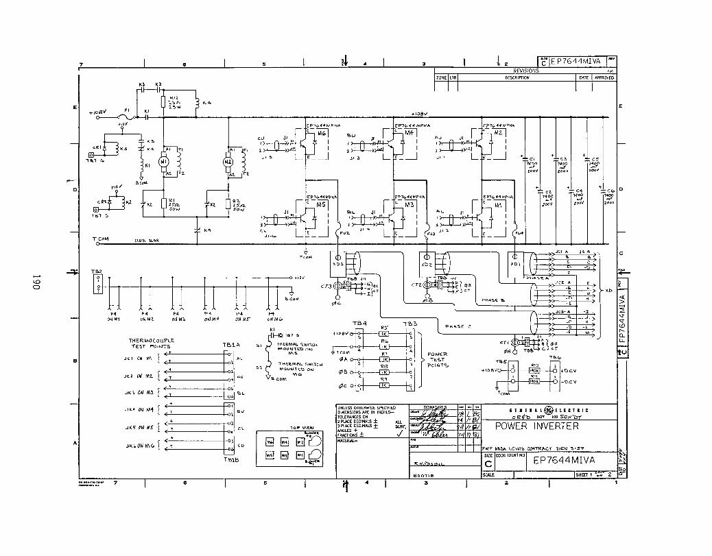
....... 1.0 o
7 e 5 il 4 3 { 2 l'CIEP7644MIVA REVISIONS '"
1-==t=4-______ -'0c=ES:::CRIPTION I_~~~~_I ~P~OVED
EI fW3
n ~~ 3"" IE
+I~! T I .'08V dfl " .. , 00
.. KI NI Ittz. r-oo 17400 1HOO ".,..f -.'f .-.1' ... '" _ ...... tOOli ZOO'l 200 ....
"T0
:
RI
", 1(3 1:: ~ ~.. ~ 3 JI ~ Lf---.J ~I 3 Lf-----1 JI I Lr---l ''''''CI I ' ..... ~~ I ...... CS
#--1 8 CoM.
o . ~A r---1 "-I I-i "-'- IE~t..'4"p.'1 IE~""4MPH'1 IE~"''''''fH'1 ~J.T7; I 'J.T7; I T:r,!; 10
B
A
~KZ ht n z,.... tK1. n 2S.n, I fc M5l I t~ M3l I To t:i.1l )OO~ zo," 1.0,"
lB.; 5
~~~ ;~ K4 t.1.. L I JI ~ .111..
E ~ ~1J2.. T CoM BU'5 'B.A.'R Jl.(p_
TeaM
11) II 1 I iI 1 I 11 lr .}:~" P4
ON Wll
7
•• 0. Mt P4
oN M, 1>4 oIJM4
p+ ON ME:
THERMOCOlJPLE TbtA T€!:IT POINTS
:: [;1 AL
(T 0,,1 AU
(i- i 051
(T WB.l.
.JKl ON M~
J(2 01J M'L
JK l. 011 M3
:: SBU
;: ~::
.JK4 O~ 1M
,](0; 011 11.,
JKIo O~ WIG,
T~lB
e
P'f oNM!.
.,
tl--K:l.".' ..
~I "TI-\E.RMA\. ':.~11l.H MOUJ\"El:lOf\)
N\S
iHEi..rt\RI.. SWHc ~ 'So 1 ~Ol)"" L~ at.)
"'CD a c.oW\.
lOP ,at..., iCOWii
8 B B"O ~ ~ ElO
.~
5
JII
~'''1~< -1-1 c:.T -I
¢"-
TB4 Te,~
T COWl
<J":t!!=O~~ rp~~'R8 " >- IK
¢c' R~ >-I ~
UNlfSS OTHERWISE SPECIFIED DIMENSIONS ARE IN INCHESTOlERANCES ON
ALL
~~(~8 ~p~CT
PHA'5.E C.
FOWER: TEST
l'QIWfS
SIG
2 Pl..ACE DECIMALS ± 3 PV.CE OECIMALS ± ANGLES + FRACTIONS ±
SURF ~ F' F' f.:' I J·I~~,.,~u MATERw..-
1<
B001\P!t
If 4 3
.... JCI A J=- A. ... --.,. Ie
_~ r Xb _ « >
JC3- " 'J: I! -s -C < _tl -L -, M.
CL W
.aU "T"Co
HIS
TClIWI

f-O \.0 f-O
7
E
o III
c
--.. B
6 5 2 REVISIONS
DESCRIPTION
:]
..
Q' Q:; ~ <J i ! ~ 1 ~ i r
0; [;-J;
~ ~ LJ8LJ
e
..
. .
I
'C'IEP7b44MIVA I .. ,
OATE I APPROYED
00', : ::1
"""" n I: Ji 1 ~ I: ~I' 1~~ : 4~ 8 J UNLESSOTHERWISESPWFlED SIGNATURES GENERAL.- ELECTRIC DIMENSIONS ARE IN INCHES- 18 I TOLERANCES ON cetD Of PI LOCSCH~ 2 PLACE DECIMALS ± ALL 3 PLACE DECIMALS ± SURf ANGLES + /
POWER INvERTER
E
10
c
FOLD --4:
FRACTIONS + V r" OC["JtfJ;, F41' f F -, MATERIAL .u",
A I II t ~ I I :::,1 1 I""" '1<' n! :.::'ri:~--t- 7 6 5 ~t 4 3 I 2 I
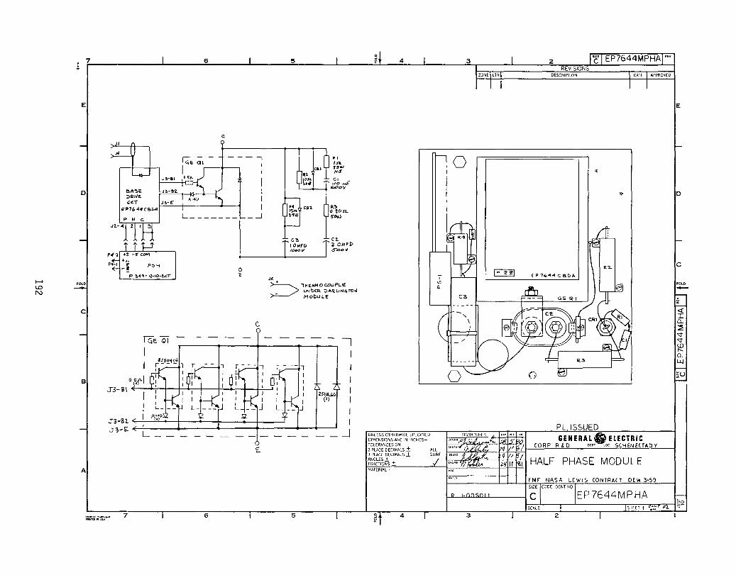
I-' I.D N
7 6 !5 d 4 3 2 "C'IEP7644MPHAI"'1 REVISIONS
E
o
,oeD
c
B
JI
""'~E '01il1'JE. G~T
.la-a,
J~-e2.
J!.-~
liP7'44C'S'DR
p ~~C!- IZ-/D-&ci
~EQ1
I
a Gf'i J3-B\
c
.., I I
L _______ L_-.J
..
c.
., In 2S"' ",.r CI
I 1 I .10 ..... -------, (,Q,OoV
1>.'> o ton.. 5"DoJ
C2-20t.lFP 5"001/
«~
:=> 'HERMOCOLJPLE _ uNbER. DA~lIN~n:hl
Mot>L.JLE'
2511U,D (2)
I
i Tt J 33-82. ~ .:....; _"_'~ 11. + J'3-t: L __
I
~
A
"'*'nr1"-O-..... l"ftIflu .. uu 7
E.
6 5
UNLESS OTHERWISE SPlCIFIED DIMENSIONS ARE IN INCHESTOLERANCES ON 2 PLACE DECIMALS ± ALL 3 PLACE DECIMALS ± SURF
:~~~i,~~ ± / MATERIAL-
~t 4
o
o
3
DESCRIPTION DATE , APPROVED
.' ,..
PL ISSUED
GENERAL. ELECTRIC CORP R &. D em coc SCH EN ECTADY
HALF PHASE MODULE
FMF NASA LEWI S CONTRACT DEW
~E ICODE IDENT NO IEP 76,q,q M P HA
E
o
c
I~
<! I Q.
~
'" '" ~ Q.
W
aU
11;;0 SHEET 1 ~."""?L . 01-
2
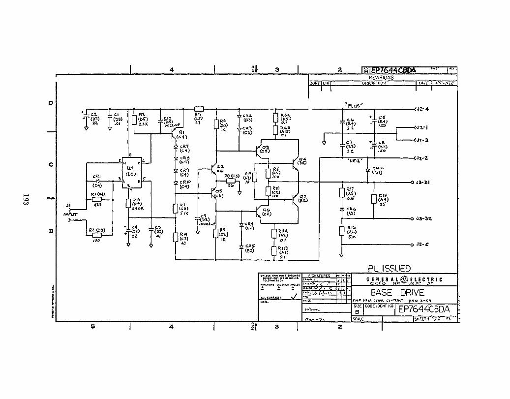
4 g 3 2 REVISIOr-:S
ZONE lTR OFSCRIP110~
01 ~ PLUS"
• J2-4 C,RZ,
R'I- (J33)
<.B'l> C.R"!> II(.. ~l)
Jz..2, c'" 'N€'4 •
CI <:101.11
C:;<:I 111' ll!.l) (C.l)
(~) 10 .I3-~1
I-' .., ~"I ~ ;'1) (1.4) w (t>+) 'ZS
2+0i(
IN,.!IT'
I~~ .... ~.) I 1,,<>4 " o J3-!.~ ~~!~.u~
c4 BI IR~ "'It~t) r(~)
zZ .1)/ IDO T 41 J. ell!> ~n-.:f.I I
J o J3-£
PL ISSUED UJrfl[SS Of .. "' .... $[ II>CC''''[O StGNAruRES .. ~ .. ~ ""
G E N(b R A L ® E LEe T RIC f'~:':~~~~ ~ ... r. I" 1111,"(1. 0 ..... .-111. I·
nACno'" O[CI"'ALI oUI4U:l , ... " .. (0 , , , r" Ct.' ~[,.,. lOC~": :>""
= = :: ISSV(O~~~_ L r I I -j J
lIllCR"~ ..... ,(\ ., " BASE DRIVE All SU"'A,CU
.,. MATLa MATL'
f ~ • Hpb .......... i '-I p""",,... ~E_ ... ~L. _ -_~ISHEET 1 • .:~:/.
5 I 4 I 1t ~ 3 I 2

...... ~ ~
.
:
,
: -+
I
,
OR.W£2
COMIrt\J:I,...,O
MOOULi.
E.P"1co,44MDC.A
I Il. ""' ~A'l
I'DBV BA" BA,rvK
-
-
PI_r:r. ACCE.LC~p..l E1t -. B'l,u:.E ~ -, OlRE'c:TloN '*
~.E ON/OfF '"*" S co'"'
~>-- COt.JTACTot -+I~V
~>- t;) C.DW\
~>-- '~'t
~ 1) 'v cr " "~ . + ;::! '
-,..,}/""QJ ~ u 0 . ~ ~ ~ ~ ~' ~
» ;::~
I· • I
I-I N __ I\!
Oo "" .,I~ ~~,....('J
: ~ djr;(J,oc I-t-J-j.- o ~
1= .. lbSV
Teo""
-
- t .. 4 I 3 I t 2 ~TEP7644S rCAI-REVISIONS
rZONE LTRI DESCRIPTION 1 DATE 1 APPROVED
I I I I I
EP 7{o4..4 MCf:.A.
CDNH.'OL .. u;:C.TIU>t.llC5 p,- , V,,,
~ VM"~1 -~
Pl .. VM, fLUX f'( ~ ,/Jlle .. h.l
'\ COIL'S Go
P21 ville ~ • y,MC. Il.n
~ 7
1 xc> \ REl."'Y , ' AU "L BU BL CU CL Hl1 <
~ 'I 'i' • t~ :1 ~ -'02
~"~N I I' ~ , '~ r ~ ~ :f .. 51 \; '" .... ""
~ ~ '" J " ~~ "' .. ~, ~' ~ ~
~ ~ t-~
.Moroe ~ dI ~ Q
T~MINFtt... ~ !-Ior.1f!
I~ t , ~ e 3 ~oA'ia.b ~ • >- ' , /!J C;1"'c."""Mr~ oN >- ,,4: ~p r:J .
u v 9 ... ~ M r-.
~I~ • v
I~ r~ .
u~ "L~ ~ ~ ~ . ,
I~ ~ .-
4 < ",!i " u ~ ~ 5 "' ~
;;; III " ~ 0: H ~ HH-; H H tJ,A1II 2i ., >-.,.. Fj ~~~ ~8
H P'I-Ip>'s,1:: A
I rJ)
POWER 1:N~ERTER <;T p"",po"S,E e. <;T
~ PHASE C
£.~'lo44N\IVA 0..
~
-
·u ~
UNlfSS OTHE.RWISE SPECifiED SIGNATURES OA' _0,. CEIEIAL@ELECTIIC DIMENSIONS ARE IN INCHES '!T :Ji. _V. '1 .5 60 TOLERANCES ON
'"''''''tJ~ '411 I corP f! B D DEPT Lee ""CHE.\J£CTA1)v 2 PlACE DECIMALS ± ALL 3 PlACE DECIMAlS ± SURf ISSU('t21A~ 1 /I / SYSTEM INTERCONNEC TlON ANGLES + fRACTIONS + j ''''''-i!fua l2ii I/~ MATERIAl- '" IF
~,~ F.,F NASD. \...E.W'~ CD\f't£AC.1 OlN'3 5 '! ~
I(' \40Ds'OLL C ICODE 'DENT NO I E P 7644 SICA ~
:no 5DDl 'eo SCALE SHEET t co::. ""
o~
.. if
...... <.0 U1
7
E
-
... o
-
....:;:
-
I 6
crQI/ cS
cTIII. ¢ c'
~ c, <> rtti
JFI )CON1A,-101Z < P4_~
~ 5.--"t'\~V 9-s COM 1-& >- -I~V ;~1),.~
CDCII. CI9I [)I"" fiR C9 FIR
c3/1
11
~E ILX4 1.L.." ~
B ~: 121('" ~~ ca < p"'-....
BI ~ ell) ~C/~:~"" 1.:1-'''-=,':.:; .. '--==--------+ F2E"Q* ~II~ f'..... R:E~ C2.G. R'So'"
-
A
IFLU~I e2.7 j~~ CI'::a
j_t> c ..
'1\.'1(1.
P. t rr <,
-tlc.~
CI'RII.
SI>
5 I l~ 4 I 3
CCLII. I ZONE I LTR I
-L I C2..B J/I
~~1~R e"Z., l Clv;r;:.--
029
~:1~8 n1
~~~~C c.3\
~J Cl4
e" I,;.
n ::J ~
l.L'o(5 ~c"'" ~ FIR c~: ~~ ::
CIO C," 'i(
~1)
III*"
CARA
CFCA
-cl·F='9~ UNLfSS OTHERWISE SPECIFIED SI~NATUR£S DIMENSIONS ARE IN INCHES-TOLERANCES ON 2 PLACE DECIMALS ±
IL\(3. I.LK.~ Il~A !N~~ ~CIMALS ± FRACTIONS +
All~ SiF~
MATERJAL-
C'4
II
of 2 I'~ EP7544MCEAI'"
REVISIONS ~¢>
DESCRIPTION
AU PS
AL ?G.
aU ?7
BL PB
C<l p~
CL. PIO
OAT[ I APpROVED
:I..LKCD
1.1.'1(.1
IL"1
'ILleS.
./" H"E~
IIjII
"'" 1L'IC.'!.
:tLH.
;lKlRAL@lllCTRIC CORP R &.0 LOC_!:I'- HtNt.l.IAUY
CONTROL ELECTRONICS
zo Sb ,0 A,a,e.. 31 ,
PI!:. Dt..l PoLl CAQ.'D TSI~" TO A, .. ,C.Ai~" ' I.,,"m'" 1 -p ON Al\..C
ft.4f NA~A LEWI~ CONTRACT DEW 3-59
111'1(0104) B
8C.Dw\
7 1 6 1 5
'TO ""1'D.1C 3.£0 QtJ "\..L CAro,,)
1 if 4
R H0050ll
B0011B
3 2
IE
I-
10
I--
c
~ w u ~
"" ~ le Cl.. w
~

I-' 1.0 0"1
E
HD
--..
B
A
7
::.= ;.v:::' 7
M\Nl:.f.O ~i.[)Ml
c.t)~i2
II
II
PIL.1tFOltA'lf.'" TOP 2.~T'OpJ\ l..b.,,£t.
IS
IS
i~ 4
\\ R:t~O~"!..~\!.
...---- t!.ACk. C.O"E~
\
ta ~ .'
~ Iq v
UNlfSS OTHERWISE SPECIFIED DIMENSIONS ARE IN INCHESTOLERANCES ON
11
2 PlJCE DECIMALS ± ALL
3 f 2
)('"
DESCRIPTION
SIGNATURES ;IIIIAl@llICTIIC
corP 12 & n OEPT LOC_ ::s.Ooft."ECTAOV
E
D
c
+---.
= w u ~ .... "'" }8 Eh au
3 PlACE DECIMAlS ± SURF 1 Y'&'fI"!- 171" f:' 1 r~,*± I ,iiQiirft • .J ...
CONTROL ELECTRONICS ..... TERIAL-
I r:: ',.~':~c"'~~l"\i';:' LUN I ",,,I.. I DEW 3 ~9 r~
EP7644MCEA I~o I CI '''''FL2i~ I HOD~OLL _ H I SHEET 2 oN
nOD",I,
if 4 3 2
I-'
~ ""-J
7
E
#D
-+
BI
AI
.... ..-11 ... " .. )
.... ,"TD101 u •• 7
II IS
1'1
" 8
I I ~~ .~ I I ) " 5'
:
IRE'/)
L--------_(D~ 0 "'"2. .. --" I I )
CI "l.l..
........
<:3 '1.1.
..... "
.: (: s~.) " F
. G
.1
.. ' y ., I I )
, I
L
It IS
ACCELc12ATlbN"
'a'R..A'lC.E. *
O\ttEc..'TIOto.) ,.
DN/OFF .,..
~ co"
cot>J'f","'QIi!...
+\5'1
1) ,.,..
-15'1
1~ 4 3 2 "'''EP7644 Moe REVISIONS
DESCRIPTION DATE I APPROVED
C:r---I ------'I
I -4
I UNl£SS OTHERWISE SPECIFIED DIMENSIONS ARE IN INCHES-
~o~~g~~I~± ALL 3 PlACE OECIMALS ± SURF ANGLES + FRACTIONS + .j
BRA(.E ACCELErZATE
--e- -I
'e.
/7'\ '-Y
FO R
REV
'/40'" (""HOL'-"»
"2.'-' -----l J __________________ 4
SIGNATURES
-roP V/C:W
PL ISSUED SIIIIAL@!LICTIIC
pp J28D DEPT lOC .seNt-wi -,
DRIVER COMMAND MODULE rATER
"'--
I"o"c~ '3.-5~
~ 4 3
E
D
c

E
tl-D
I
I ...... -+ ~ CO
B
A
7
CLl 5.0 " ... ~
CHI
I REAL l< > CI1
T c~o
ov AOl
... "
+I~Y
.. ~ I~K
R~'" I~
6
/11~ cc.
C1
al,,/r/
r
/FLU~I ) - .'8 C L ~r-,..a ~ ,1r::J
YocT
::=;'":=:' 7 II
+I~.
... '''''
i5 1~ 4
*IS"
-~,t.J.
SrE"~b
or
c.~.12
I~~
5001l~
3
-::-
~~o lOOK
~
t 2 .... EP7644CAR
REVISIONS DESCRIPTION DATE I APPROVED
::i 11 t ~+_ )C.\lD
-=- .,':.'1 reD so
R4.5 11.~CLl. ~ ,0 '~K LILU
R., ,~<
R~L
•• :>>l~ ~ ~) CIl.
E
o
c
+-
I~ <{ U <3" q
j":. 0.. W
II +\~... I cn~ nut 41~~ 1 L;'i.-'f {IWIL
~ .. 0 La FT
\111 ""~ lAI>
" '6V
/1 ''''I 77S0
o 157 I.A "'Z 74 V
-J/""·"/Iiiu • "./FLU,.j
'D~' I I ",",,"""'- SIN .. ,~ ~
nt.) F"LU~' ,g;+".l 1. c. -
~5V 1.1.-4'
l' C~~ -\~"
41 ..... ~ RE"SE"T "1:.'hT(FLUX <MIN)
75Zz.
1"~7
o 31.n , '14
-::-
PL ISSUED ~* IN S.TI'toLL JUW\pt;.2 W\~£
C"~"C\TD2 OPTlQKJtrr.l.
UHLfSS OTHERWISE SPECIFIED I.'4n DIMENSIONS ARE IN INCHES- ; £ • £ • A I ~ £ I £ CT. I C ToLERANCES oN COR PR&'O .om IDC_SCHENECTADY
~~1.1 nllY.' 2 PlACE DECIMAlS ± ALL !,,~~CIMAl..S± SURF ANGLE REGULATOR FRACTIONS ± j
OFLUX)- 0" /:r/ J l[~~~- 181 1M)
B
MATERIAL-
if 4
W. KOHLER EP7644CARA ~OO'''2.1 SHEET , ~!j' rL
3


N o o
A
~
B
c
o
E
2 3
1001\
EI"'~l..~
-v\~~--
1:,4)°" ~ '''0 IIII~
r~4f~ ~H IIII:J
tlSO
'l:
GEN'£ ~#N'.$drJ 111<1' ,
'liD
""~ GENERAL@ElECTRIC 1~:'?:'.",4 CC:~ 1
CURRfN r LIM IT A~" L .... ,,~ :!J 5"
pi.,., I N"'~[ DRAWING NO DESCRIPTION "'U(A'AL. WEICHT <tl
~!!ill!!I~~~=i~~:::::::::::=::::::::::::::==::::::::::::::::=-~C~Z3(~LL'_ r , ... , "'« '"_0 )" C;;:;::m f" '" 'I L .....
f..!2..(~\1\ Iw'NoJr,J
"'~f.' "'~
~.,'" Y~ lll~- I
1 1_ ~ ~
')'< I l' CZ (~iIII>
~ c.~~ R'I't
~ 4)C3<.. C''' "so 'T T~I'c.~
~ c~z. R4l -;-0 ~ ~ Ie) ..L -L~_, tIS
~~S"
~)C~ ~.lt± ~T J?44 -15
... • ....... u ... 2 3
~ ~ ~ ~ -;:
rf-rlolJ..J(4
~~fJ;LV
PL ISSUED O[SCllIIPTION Of"c;.ROU",

N o .......

7 II !I
EI ·'5'1...5'1 ~ ""E:Le:~re ..
C30
410,1( 1!RAKE ..
CLB .'"
~I o.lo.f~ - ~ R2.0 ilJ 5'1 "7oK t'~ 2.101<., IK +ISV U4 •• I
+/5v
FReQLlEIJ~i ,,<1-
CIO N ~I
1..17
0 N
",,0"-
IFLUX/~ '. Cl~ ... Ll~
~
U<a
BI ------., J: RE""'L 1't"
(D)
OoJ/OFF lI-C'2.0 ) D r~ <,. c»i~
LIB AI
t>1i1e:<1"I0I'l *" CI~ ) --I ~~
US
~ ¢ .. - ... ., .. ~ 7 I II !I
IT 4 3 :}.2 I clEP7644CDCAMV
REVISIONS X DESCRIPTION DATE I APPROYED
-tISW i&1)
~ ----_----;) I REA.L * CI.
.0
IK U3 ::t. RE:At.,. *:-
,,'- "'iW"-RE
I RE:'Al..""O CI1
~o" 1"1S~
II V ¢
• A;L~(+IS'\ en U'3 IOA.L-H
C, c:'2.
S'bfUQ IQ_f
(ES) ~~: ) '" C," l. 1. C4
Ll. l4....f1 Io.o11 ..... f A~~ IU __ ~ ~ > (-IS"V) C3" :>-u.uJ 1 K ::.21
" /';'0 .J
+\~" R"B "Co
F"Wt) ~ ><..
II./I(/
CC\~
I I 1.,;;1L--Ul~
II.~ l Cl,,\-I tlE"L'J4:-0
~ 1~50"Z. S PillA ~ I c/~ -----""----
UNLfSS OTHERWISE SPECIFIED DIMENSIONS ARE IN INCHESTDU.RANCES ON
ALL 21UC£ DECIMAlS ± 3 FUCE DECIMAlS ± ANGLES + FRACTlONS ±
SURf'1 ~ FjU E'I j ,........ . ... MATERIoIL-
.. SOO~I(g
~ 4 3
DRIVER COMMAND & JERK LIMIT
IE
1°
Ie
U 0 U <J"
3 r--CL W
fu

N 0 ...
0, ~" ~ 13
It.
F;'uJC -., A C~
FLIJ'f., ~ ~
C'5 #-- -/
R~I
- B I ~
FLU~ ~ C C8
el.1 I:~ ~I> "1.10
-1, rt58
< -'1'"'" _. ~ - mw '.
D
II:
~) "" ...... cU.
=:::..
IJ 'J "'"
R.b ~(£!, S-
- 1'<1"" ':'0 C. 21.l 126 ~ + " ~ ,eK ~ I .... h
L+
N(m:
z
R1G. ~Ul)"'tO~" t.0Ml"l:T't't) ~O C"'\aC(o
3
rlPST MACE FOil Nfl,
t5£A..I£ .;;TP,JhJ~.:''''17/1.11-1'..
XF
~-<
DRAWING NO DESCRIPTION I'IAl(R,,lI.,W[IGHT
L-----------------------------~~IFLUXID RH Ii: .9) I'-LUX I
-n>'" ;')." + »-IFLUX \
Ci
I-==========~__ r---------")>- I :q .. cza
- ,
W II<.
+15D
CII
C~P<"':'3
<,iJANlX.'"'l
IS
~>CZ~
---i~II\@-;IK .. ., ~~
'>"~ 1>-c)o
~
PL ISSUED OESCItIP'T1DfIIOf' GIIIOU,", .[VISIONS

5 !~ 4 3 ~2 IC'[EP7644CLOA 7 8 REVISIONS fC
It.. .... B27 )~-----------------------r------, DESCRIPTION DATE APPROVED
1.~- B"e
J.~co.DBI'l cr.'-- ern"' L~ \'''"'1\ ........;...,.ran IE E I ." i"'"i I u, \ u, ,),. '.1. q)A
I""r .'5
Bip Oi,Ji I..J"PE~
A.(.,. Jeer
¢~ 8
1,- Our L.owl!R,.
, twt.. RET
01 1. B- '" ' '~ ~ TISV 10 e.14 RJS"
~ ~ ¢ IS C::o"";' 8/.. U I nO/l( 8 11.01( e f?Z ~ BIS OLJ; UPPE'R..
;~i , "a, ,,' C'" " '" t ~W) ¢~
Il BZ4 Qu; L.OWE"R... 41 ~ Ali RoT N TIS< ,. ~ ~ ,,~ ~.:.~ I~
Ie " .," a ; .,110"- 7T au", I \ <- - I~ "'or-! ~Q~ ,,~'" I (/.c I:g:
IC'.MD
B" U ,C ' <J <J ~~~ (BY) \ \ I I "-" ,.10s<-,. I B30 OuT uppeR. ~ A;o ~€'T CL
W
B 1 c, 0 c t:. A. 320 >--.--.l'P')Ic.
.!U
¢c.
~ "".~~~ fOf! co'" All_ ~Ei s€:.c SH Z.
'S bet.' 10 I UNLfSS OTHERWISE SPECIFIED SHuT Do""~ DIMENSIONS ARE IN INCHES-
~~~~g~~,~lts ± ALL 3 PlACE DECIMALS + SURF,
I A ~ C >--tSv DIC,l1.L ~~:6ib,* ± - J 1-.1"~"''''W'~'tlj~%~--f-fu'-1</I''-,I!f~-'-1,1 LOCK-OUT & WAVEFORM GEN, '?z. ABc.. >-- +ISV AH-"I-o,"" MATERIAl-
A I ILK(Q C 1.9 >""-l ~-=. A a c >-- "tIS" DIl.:!I,."L
ILK7 C,or-J "S' :S~~C >-- -IS'V SIZE EP7644CLOA ",," B<. >-- Go"" eo.. 1-.J:.JJ<i:"'"'1J.l.-----t;C;;)..._-,r-.J ______ T.:;;;;;;-;~;;;r._t
~ BDO(QI(£) SHEET 1 c,~ Z.
7 8 5 it 4 3 2
N o ""-J
7
E
-
01
~I
-
B
AI
I 6
+1501
"", ... (HP) ,K
RL.~
(HPj LK ...
I 5 I
9,. ~D Ulc,QI' , )<14 CCO<:.I<.A
lHS)
~I I " I ) Co' ~ C I.. oc" I>
-4q~ .r--W(,t' (II') q
74n .• QC
,...!-j. Q"~ 00
~
FE!Ii~,t )>-----------------'-NP-U-':-l DUWl>'
t I ~V
ABC 30, hr--~---T- "51/ DC. <N
» 4 I 3 '::2 Ie I EP76,q,qCLOA r-I REVISIONS ;"
C>1. (~"-) 24p~
-r x.TAL Y1~ Go 000
"'Hi
.. H (~
e'3 (.t\fP..) S"~f-
1<4. (A~!!;" ...
Q3B (BR)
__ s.. . ql4 "I"-J , .. ~ Tlsse
UIB {J.P)
8748
E'"
~T1
Fie cS ~
1...01( 'TO
CR1. 5 ~ (UNDER ~) r'~
+ S ~ I/IT
R51
rZONE I LTR I DESCRIPTION I DATET APPROVED
I I I II
~ I , PH"""€: A I R47 ,I tll\C. (E"') R~
,q! 714.
I ~C~ 'Vot..T" I LJ I'! 017
: (1:>") J /0',':2. 'I I
-'LL t>AC. ~ PIN.~
",IS/I{"',17,/8 TIT T'IREF' e.( ALL I>AC.,5
!±
~ PHA~e: e. fc~~ ote ~ '" _0, o "" C4 4 \.l2.0
3 (HI z I
~I
A~;N't)~CS +15v -=R"" -\lRE.F
ALL!:)~'S-15"-1 I i I l(A.LL.. b"C.~ PlO 2/ P~N 10 If
Pl.1 2Z. I~ PH~~e: c ,,4~
)~:l ec
~IZ c. ..
P/1. 13 "" D ... C. PB 24 5 P/4 35 4 PZ5 !I. 3
PI ... 37 Z Pl738 I
cZO (c£.)
LJ Z I (H:) C"
C ... ·) JOI ......... +
E
r 10
I-
c
~ C§ -' U ~ ~ to I'-!l..
~ ~~,. lC~\
~;~ ~~~\T >-D-----r -r_""""'~-O::.OI-. ~ l~<:'\ t4Nt> PIN~ 5'J/~I"J ,4
'2..N3.~D4 +SV PL ISSUED UNLE'SS OTHERWISE SPECIFIED SIGNATURES DIMENSIONS ARE IN INCHES- 0Il0l.'''11 ~ .,,,b;.. , I I&l ~op~~g~~I~LS ± ALL CllECIIU t:e~;. II I 3 PLACE DECIMALS ± SURF, ,~" J!. ~ t f II
I~~:~i,~~ + .j "-Ilf'IWM W 111.'11 LOCK-OUT & WAVEFORM GEN MATERIAL- "nil
--.------r-- -'-IREF
GENEftAL@ELECTRIC c...g~'D DEPT lOC SC.H'Di
/25Z. (541 )
R53
71 3.t.l1 crt 21<. (EN)
'C"- III~ >---D-10K
~ J .... ~ .eEF FMF N~"""'~ L.eW~ CoNT~,h,C.." be-tV ~·59' ~
-1$'1
SIZEiCODE IDENT NO I 76 /I /I 0 • ~ RI10D. C EP yyCL A ~ U~, ~
80052.1 SCALE -)" I SHEET '2 c:tv FL c~
7 I 6 I 5 I if 4 I 3 2
N C> co

;:,::::,,'::':' 7 ,-6-,- S - ._[ it 4
N ..... o

7 6 5
E
L
RI4
L
0.1.0
l
l~ 4
.. " ~
-1... A. 1 (100 AI>!) 1t24 ..
CI"
=::J---O 1 ~ ~ I. .,Co R"" =:::J--C:J--L .~ 390.»- :;-
-I B1 (IOOA/v) 1(1~ en
~ll!>~ II:'
Rt1
~ 1'< .q '30 on,.
·'I.c.i. (100/11,,) CI">
l.c I
UNlfSS OTHERWiSE SPECIFIED DIMENSIONS ARE IN INCHESTOLERANCES ON
3
2 PLACE DECIMALS ± ALL
3 PlACE DECIMAlS ± SURF I ~ f'" I" t! I ~~~~~I~~ ± ~ .~r.~ .. MATERlAl-
\o\J .:..t""'LE2
800,,"04
if 4 3
f 2 EP7644CTIA' ''' REVISIOI,S IX J
DESCRIPTION I DATE I APPPOVW
PL ISSUED GIMIIAl@llICTRIC
CDi!P Ii? BD O[PT lOC 5CU£AJECTI\D
CURRENT TRANSDUCER INTERFACE
E
o
c
~
H fU <;T <;T
Ie (L
w aU

51.</£ ~qA/"'N 311<1.... XE
l{1iii"'7~td3 2 3 GENERAL@mCTRIC EPlt.44 C T6\A ~.,.- ~'. ..,
• UJI 10 C'oN1'"-"'II.c.r 3-
DR~WING NO O[SCRIPfiON I ..... T(RI~L WEIGHT
A :.~
V",. (31
~ A ~ , O+I$""
CIO fIR ~
B t~i ~ 11 ~-- CIi'r- r,ux A ~o II ~~: ;:: :~~: ~
CJo V",!, ~
<14
G>-INU<+ 'U
N --=01 ,,:.;r '1"1 31 ~ I ·':~l 1 1 1 - I >-ZNli\ 5' ....... W C
,.a.., I ~ _ I ~4 I I .........r .. -"'\.-- CQ
>"'~-~>-.
V\(\C C~tg ; ::~ U8'" ~.. @'R~l
~ I) I - J C.,
AU, " +"1 U~ " >- Ie.
-'1" (/~";')IA ~
R~7
D 1 !] f ~ Cil 75" 1 (Ill) "", .. /II ~"> ", ,.,
i~ .1.1 ell I~ ~~ .. st.""rATt it»J$
FROM [0:5] '2~ _ 'I_~I. To PtM 36
5uMw..,"G -.!L 'NlPLlm"~ ~:) .. ' (~) -s I .'"" ,74l n.~ I 0" ~T~ I.lul) SoAN
t~1 ...., ~
= _j ~u PL ISSUED C3'Z.~ ~ DESCRIPTIOtrtO'GROUI'S R[Y1SlOMS
-?~ ~~./IS S atTLlIt~ 1 c... ;E-' I"· .. E ~> C~ c.& ..
,,~ '-''''"I -"12"1 t ~ -:lei. ,,(: 'Z. c~ 2!: ..,...Y;'; "T"c'f 1,J
~~- I Ie. L.nn.. eZI I eooc.o~
fis.--1- -"o2LZ... SUMNllt.lG AMPlifiERS,
2 3 1+4 S

Appendix E
AC CONTROLLER PRODUCTION MODEL COSTING
1.0 INTRODUCTION
A slgmficant portIOn of the hfe cycle costs of the ac controller IS the productIOn cost of the hardware This appendix detaIls the ac controller costIng based on the scahng done In SectIon 3 9 The summanzed results are presented in SectIOn 3 10 The costs presented are In 1980 dollars
2.0 COST CALCULATION OF MAJOR FUNCTIONS
2.1 INPUT CAPACITOR COSTING
2.1.1 Summary
The cost of the Input capacitor bank IS hsted In Table E-1. The cost is for each capacitor purchased In quantItIes of 1000 or more The costs are extrapolated from the capacitor volume and are approximatIons which can vary 10-20%. Recall one capacitor bank IS needed per vehicle
Table E-1 INPUT CAPACITOR BANK COSTS PER VEHICLE
NomInal Battery Motor Horsepower Voltage
10 20 30 40 84 $51 $90 $127 $168
108 50 87 129 169
150 37 67 98 129
300 37 61 80 99
2.1.2 Assumptions
1 The capacitor bank volumes would be avaIlable as required
2 The capacitor IS an alumInum electrolytIc type
3 The capacitor bank IS represented by SIX IndiVidual capacitors
50 $209
210
159
115
4 The indiVidual capacitor cost represents one sixth of the total capacitor bank cost
2.1.3 Calculations
After consultatIOn With the apphcatlOn engIneers at Cornell-Dublher's alumInum electrolytIcs manufactunng faCIlIty, their InformatIOn Indicated that for all alumInum electrolytiC type capacitors rated above 60 V, the cost appears to depend only on volume (13) An equatIon representIng the cost IS
$C = (0476 VoID 847) X 6
215
Where,
$C = capacltor bank cost In dollars
Vol = one slxth of the deslfed capacltor volume
2.2 POWER MODULE COSTING
2.2.1 Summary
Table E-2 lists the estimated cost range for a power module at dlfferent system ratings. The costs are approxlmatlons based on the per square Inch cost of sillcon, packagIng, Yield, and adders which are extrapolated from device costs of the General Electnc D67 power DarlIngton transistor and a fast recovery dlOde The costs are for a 60,000 to 600,000 annual quantlty, recallIng that SIX are needed per vehicle Use the upper range for 10,000 vehicles per year and the lower range for 100,000 per year
Table E-2 COSTS PER POWER MODULE
NomInal Battery Motor Horsepower Voltage
10 20 30 40 50 84 $40-65 $81-130 $121-195 $162-261 $202-326
108 39-62 77-124 116-186 154-248 193-310
150 45-73 91-146 136-219 182-293 227-365
300 41-66 82-132 123-199 164-264 205-330
2.2.2 Assumptions
1 The sIlIcon area of the fast recovery dIOde lS represented by 45% of the sIlIcon area of the maIn power device
2 The sIlIcon cost of the dlOde IS 2% that of the maIn deVice
3. The diode IS packaged In the power module with the power transistors and, therefore, the effect of module Yleld is considered In the total cost
4. Cost estImates are based on 1980 dollars for quantltIes of 60,000 to 600,000 modules annually
2.2.3 Calculations
Cost estImates were obtaIned from the Semiconductor Products Department of the General Electnc Company, Auburn, NY. The cost estlmates are for the D67 blpolar power Darlington transistor The costs lIsted In Table E-2 reflect those associated wlth a developIng technology and such effects should be conSidered In "future cost" predlctlons, I e., the wellknown learnIng curve, as dlscussed In SectIOn 2 6 The 300-volt rated module w111 stIll require module costs proportIonal to the SIlIcon areas.
As a guideline, the silIcon cost of the D67 transistor is used as a basis for module cost The projected cost of tested translstor chlps and dlOdes, module matenal costs, labor costs for
216
assembly, and associated module YIelds are combined ThIS combmation IS used to estImate the cost of a power module havmg 1.91 cm2 (0.75 m 2) of silIcon area (excludmg the fast recovery dIOde). The module cost IS proportioned to represent the 1 98 cm2 (078 m.2) sIlIcon area module for the 20 hp, 108 V applIcation This cost IS assumed to be the base value and wIll be proportIonal m SIlIcon area to the cost of the other dnves These costs are for volumes rangmg from 60,000 to 600,000, smce there are SIX such modules m one controller. The costs are
SIlIcon and packagmg matenal costs $65.00 - $105.00
Labor mmutes for assembly and test = 5 mm
Labor costs at $21 00 per hour
Total module YIeld 90%
Module cost for 1 91 cm2
(0 75 m 2) of SIlIcon
$ 1.75 - $ 200
$66.75 - $107.00
$7400 - $11900
The module cost for the 20 hp, 108-volt rating with an estImated 1.98 square cm (0 78 square mch) of SIlIcon is wlthm a range of
(078/0.75) $74 = $77
(078/075) $119 = $124
2.3 POWER MODULE SNUBBER COSTING
2.3.1 Summary
The costs of the different snubber networks are extrapolated from the 20 hp, 108-volt base values The costs lIsted m Tables E-3 and E-4 are apprOXImate because of the assumptIons that are needed to make the calculatIOns possible Recall that six such snubbers are reqUIred for each vehicle
Table E-3 COSTS PER SNUBBER FOR 10,000 VEHICLES PER YEAR
Nommal Battery Motor Horsepower Voltage
10 20 30 40 50 84 $564 $11.28 $16.93 $22 57 $2821
108 4.63 925 13.88 18.50 23 13
150 363 726 10.88 29.03 36.28
300 235 4.69 704 939 11 73
2.3.2 Assumptions
1 The present 20 hp snubber deSIgn uses components selected for their optimum characteristics.
2. The charactenstic waveshape of voltage and current seen by each component does not change for dIfferent ratings, only the magnitudes change.
217
Table E-4
COSTS PER SNUBBER FOR 100,000 VEHICLES PER YEAR
Nommal Battery Motor Horsepower Voltage
10 20 30 40 50 84 $4.56 $9.12 $13 67 $1823 $2279
108 374 747 11.21 1494 1868
150 293 5.86 879 11 71 1464
300 1 89 378 568 7.57 946
3 The total costs of the resistors, capacitors and dIOdes are representatIve of their Thevenm equivalents and wIll scale appropnately
4. Cost of packagmg IS neglIgible compared with parts costs
5. The costing is based on 60,000 and 600,000 annual quantIty
2.3.3 Calculations
Listed in Table E-5 are the indiVidual components and their cost used m the 20 hp, 108-volt snubber network. These costs were denved from dlstnbutor catalogs and adjusted for
Table E-5
BASE SNUBBER COMPONENT COSTS
Type/Quantity 60,000 600,000
Semiconductors 1N3913R $572 $462
MR856 0.79 064
TOTAL 6.51 526
Resistors 5 fl, 25 W 0.39 031 15 fl, 25 W 0.39 031
02 fl, 50 W 076 062 10 fl, 50 W 059 047 TOTAL 213 1 71
Capacitors
0.022 JLF, 200 V 0080 0064
0.22 JLF, 200 V 011 0092
20 JLF, 200 V 042 034 TOTAL 061 050
SUM TOTAL 925 747
218

quantities of 60,000 and 600,000 Adjustments are made by usmg the graph m Figure E-l. The cost values appearing for other dnve ratlOgs is approximate Because of the complexity of an optimum snubber design, only a logical deduction of CIrcumstance appeared as an adequate method to project costs This logical deduction IS as follows
W, o 9
ii: 8
a.. W • > 4
~ ..J W 2
a:
I 2 3 4 5 6 789
I 4 56789
QUANTITY
2 3 4 5 6 789
Figure E-l Relative Price vs. Quantity
I 2 3 4 5 6 7 e 91
The snubber IS assumed to absorb a constant percentage of energy from the dnve system dunng power sWltchmg and the eventual dissipatIOn of this energy (or a constant percentage) IS done m the snubber resistance. Power diSSipation m a resistor IS proportional to the resistor's surface area The resistor's cost IS proportIOnal to ItS volume. Therefore,
Where,
$ cc Vol cc Area cc Power $ cc Power
thus, $, = (HP/HP b) $,b
$, = DeSired cost of eqUivalent resistance
$,b = Base cost of snubber resistors
The absorbmg of energy by the snubber IS, m part, stonng of energy m the snubber capacItance. If the system voltage IS held constant, then, m effect, by paralleling snubbers the capacitance becomes proportIOnal to the horsepower. Capacitor cost IS traditionally proportional to ItS CV product (capacitance and voltage ratmg) Therefore, for constant system voltage
219

$c = (HP/HP b) $cb
Where,
$c - desired cost of eqUIvalent capac1tance
$cb - base cost of snubber capacitance
If the system voltage 1S vaned and system power 1S constant, the snubber energy storage remains constant This mdicates the capac1tor value vanes mversely as the square of the voltage to mamtain a constant value of energy bemg absorbed The capac1tor cost vanes as the CV product The resultmg cost change is'
$c - (EbIE) $cb
Where,
=
base value of battery voltage (l08 V)
des1red value of battery voltage
The total eqUIvalent capacitor cost 1S.
$c - (HP/HP b) (EbIE) $cb
The d10des w1thin the snubber network should maintain constant current dens1ty within the sllicon The vanatlOn of reqUIred slhcon area due to voltage change 1S cons1dered neghg1-ble. Therefore, the dlOde 1S assumed to scale directly w1th current, mcreasmg or decreasmg the silicon area to mamtain constant current dens1ty The cost of the dlOde would scale as a matenal cost proportional to slhcon area (Packaging cost 1S neglig1ble) Therefore,
$d
Where,
$d
$db
-
-
desired cost of equivalent d10des
base cost of snubber sem1conductors
The snubber network cost 1S a combmahon of all the eqUIvalent components' costs Thus,
$ sn - (HP IHP b) (E blE) ($ cb + $ db) + (HP IHP b) $ rb
Where,
cost of snubber network
2.4 BASE DRIVE COSTING
2.4.1 Summary
The base drive costing includes both the base drive C1rcUlt costs and the base drive power supply. The base dnve c1rcuit is broken down into the common parts and the required output driver trans1stors Recall six such base drives and supphes are required per vehicle. The costs over the voltage and horsepower ranges for 10,000 and 100,000 vehicles per year are shown in Tables E-6 and E-7 respechvely.
220
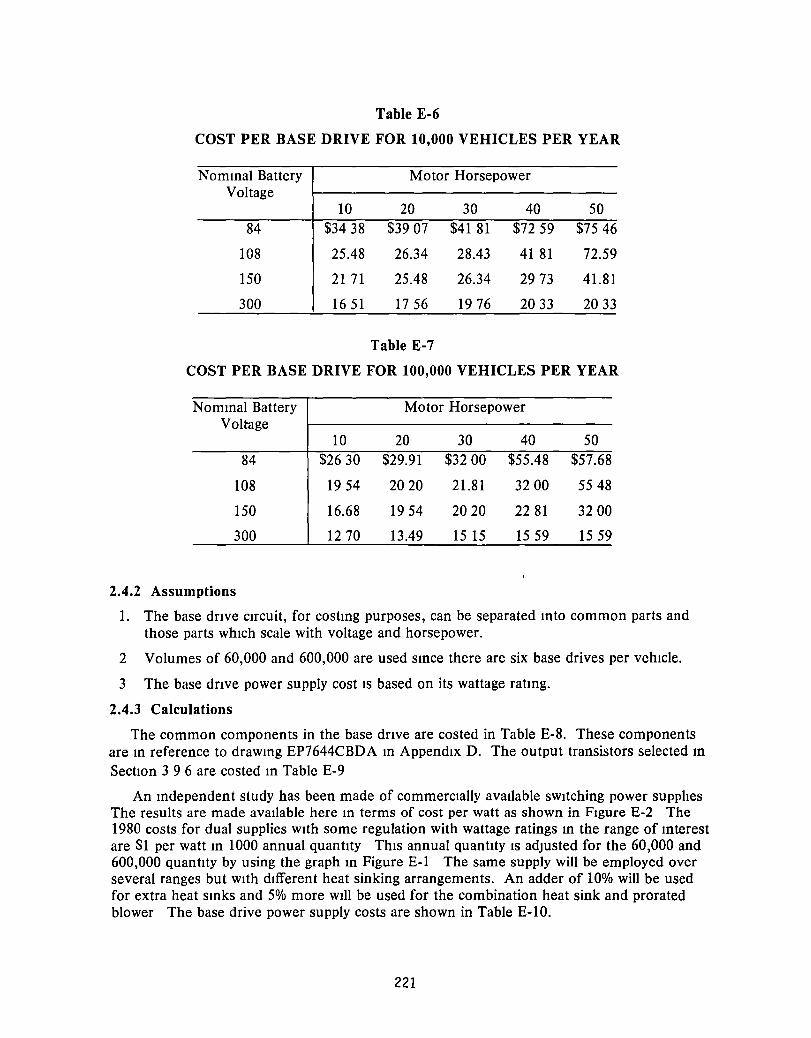
Table E-6
COST PER BASE DRIVE FOR 10,000 VEHICLES PER YEAR
Nommal Battery Motor Horsepower Voltage
10 20 30 40 50 84 $3438 $3907 $41 81 $72 59 $7546
108 25.48 26.34 28.43 41 81 72.59
150 21 71 25.48 26.34 2973 41.81
300 1651 1756 1976 2033 2033
Table E-7
COST PER BASE DRIVE FOR 100,000 VEHICLES PER YEAR
Nommal Battery Motor Horsepower Voltage
10 20 30 40 50 84 $2630 $29.91 $3200 $55.48 $57.68
108 1954 2020 21.81 3200 5548
150 16.68 1954 2020 2281 3200
300 1270 13.49 15 15 1559 1559
2.4.2 Assumptions
1. The base dnve clfcuit, for costmg purposes, can be separated mto common parts and those parts WhICh scale with voltage and horsepower.
2 Volumes of 60,000 and 600,000 are used smce there are six base drives per vehIcle.
3 The base dnve power supply cost IS based on its wattage ratmg.
2.4.3 Calculations
The common components in the base dnve are costed in Table E-8. These components are m reference to drawmg EP7644CBDA m AppendIx D. The output transistors selected m SectIOn 3 9 6 are costed m Table E-9
An mdependent study has been made of commercially avaIlable sWItching power supplIes The results are made avallable here m terms of cost per watt as shown in FIgure E-2 The 1980 costs for dual supplies wIth some regulation with wattage ratings m the range of mterest are $1 per watt m 1000 annual quantIty ThIS annual quantIty IS adjusted for the 60,000 and 600,000 quantity by using the graph m Figure E-l The same supply will be employed over several ranges but wIth dIfferent heat sinking arrangements. An adder of 10% will be used for extra heat smks and 5% more wIll be used for the combination heat sink and prorated blower The base drive power supply costs are shown in Table E-10.
221
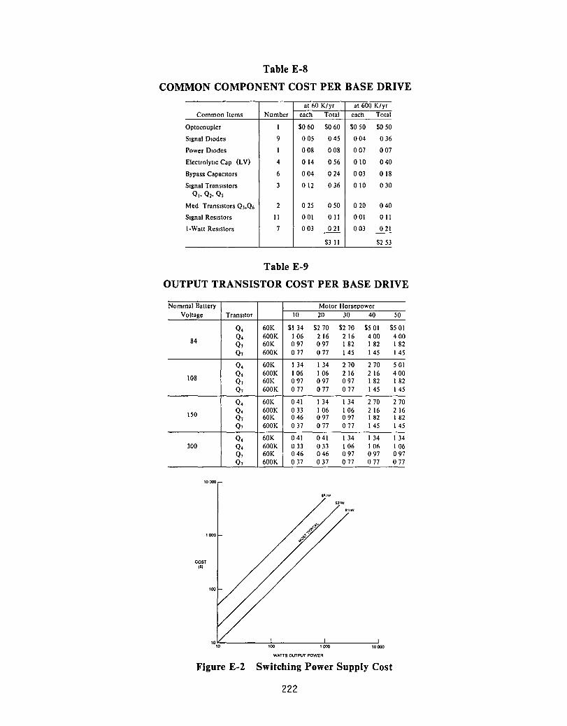
Table E-8
COMMON COMPONENT COST PER BASE DRIVE
at 60 K/yr at 600 K/yr Common Items Number each Total each Total
Optocoupler I $060 $060 $050 $050
SIgnal DIodes 9 005 045 004 036
Power DIodes I 008 008 007 007
ElectrolytIc Cap (LV) 4 014 056 010 040
Bypass CapacItors 6 004 024 003 018
SIgnal TransIstors 3 012 036 010 030 Q,.Q2.Qs
Med TransIstors Q).Q6 2 025 050 020 040
SIgnal ResIstors II 001 011 001 011
I-Watt ReSIstors 7 003 021 003 021 -- --$3 II $253
Table E-9
OUTPUT TRANSISTOR COST PER BASE DRIVE
Nominal Battery Voltage
84
108
ISO
300
10000
COST is)
Transltor
Q4 Q4 Q7 Q7
Q4 Q4 Q7 Q7
Q4 Q4 Q7 Q7
Q4 Q4 Q7 Q7
Motor Horsepower 10 20 30 40 50
60K $134 $270 $270 $501 $501 600K 106 216 216 400 400 60K 097 097 182 182 182 600K 077 077 145 145 145
60K 134 134 270 270 501 600K 106 106 216 216 400 60K 097 097 097 I 82 I 82 600K 077 077 077 145 145
60K 041 134 134 270 270 600K 033 106 106 216 216 60K 046 097 097 182 182 600K 037 077 077 145 145
60K 041 041 134 134 134 600K 033 033 106 106 106 60K 046 046 097 097 097 600K 037 037 077 077 077
S5'W
11fW
10000
WATTS OUTPUT POWER
Figure E-2 Switching Power Supply Cost
222
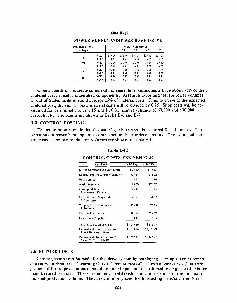
Table E-IO
POWER SUPPLY COST PER BASE DRIVE Nominal Battery Motor Horsepower
Voltage 10 20 30 40 50
60K $1700 $1870 $1964 $3740 $3927 84 600K I3 57 1493 1568 2985 3135
108 60K 11 20 1176 II 76 1964 3740 600K 896 941 941 1568 2985
150 60K 1018 1120 1176 1176 1964 600K 814 896 941 941 1568
300 60K 679 747 747 784 784 600K 543 597 597 627 627
CircUIt boards of moderate complexity of signal level components have about 75% of their materIal cost In readIly IndentIfied components. Assembly labor and test for lower volumes in out-of-States facIlIties could average 15% of materIal costs Thus to arrIve at the expected materIal cost, the sum of basIc matenal costs wIll be divided by 0 75 Shop costs wIll be accounted for by multiplYIng by 1 15 and 1 10 for annual volumes of 60,000 and 600,000, respectively. The results are shown In Tables E-6 and E-7
2.5 CONTROL COSTING
The assumptIOn IS made that the same logiC blocks wIll be reqUIred for all models. The VarIatIOns In power handlIng are accomplIshed In the Interface circUItry The estimated control costs at the two productIOn volumes are shown In Table E-ll
Table E-ll
CONTROL COSTS PER VEHICLE
LogIC Block at 10 K/yr at 100 K/yr
Driver Command and Jerk LImIt $ 25 30 $ 18 15
Lockout and Waveform Generator 42524 378 02
Flux Control 873 686
Angle Regulator 313 26 19562
Zero Speed Detector 2530 18 15 & ProtectIOn CIrcuIts
Current LImIt, Magmtude, 4161 3172 & Controller
Torque, Current Interface 10398 7883 & Summing
Current Transducers 28164 22907
LogIC Power Supply 2043 1675
Total Expected Shop Costs $1,24549 $ 973 17
Control wIth Interconnections $1,37004 $1,07049 & and HOUSing (I 10%)
Control with System Assembly $1,50704 $1,14542 Labor (I 10% and 107%)
2.6 FUTURE COSTS
Cost prOjectIOns can be made for thiS drIve system by emploYIng learnIng curve or expenence curve techmques "LearnIng Curves," sometimes called "expenence curves," are proJectIOns of future prIces or costs based on an extrapolation of historIcal pricIng or cost data for manufactured products These are empincal relatIOnships of the cost/price to the total accumulated productIOn volume. They are commonly used for forecastIng pnce/cost trends In
223

commodIty type industnes (I.e., semIconductor, electronIc components, plastics, consumer products, ferrous and alummum matenals, metal parts, etc) where production volumes are large and the effects of technIcal mnovatIOn, manufactunng productivIty and volume growth are expected to contmue as drivmg forces to reduce costs
Learnmg curves are particularly applicable when the process mvolves 1) Repetitive OperatIOns 2) HIgh Dlfect Labor Content 3) HIgh Direct Labor SkIll 4) Long Production Runs 5) Reasonably Short Cycle 6) Complex Product
At least at the start of the productIOn of thIS dnve system, the learnmg potential IS high because of the condItions mdicated in Table E-12 Areas of learnmg potential for both portions of the fabrication process are those shown in Table E-13.
• • • • •
Table E-12
LEARNING POTENTIAL MATRIX
Operation Man-Paced
Machine-Paced
Direct Labor High
Low
Mgmt and Innovation High
HIgh (Between Lots)
Table E-13
LEARNING POTENTIAL AREAS
Direct Labor Mgmt and Innovation Job Knowledge • FamIlIarization
Dexterity, skIlls • EliminatIOn of Bottlenecks
A vOIdance of Errors • Product DesIgn
Bad PractIce A vOIdance • Process DesIgn
Potential Trouble • Tool, Jigs, Fixtures Detection
Some classic expenence for types of assemblies are listed m Table E-14. The expenence is expressed in terms of the percent of the learning curve, which IS representative of the rate of price decline (slope) of a price versus volume learning curve A typical price "learning curve" for a power semiconductor device IS shown m FIgure E-3. In this illustration, the modest price decline shown during the mitial productIOn phase reflected a strategy of pnce protection to recover the development costs. As competitIOn mcreased, the price declIne became steeper in order to protect market pOSItion and was more representative of the actual "cost learning curve."
224
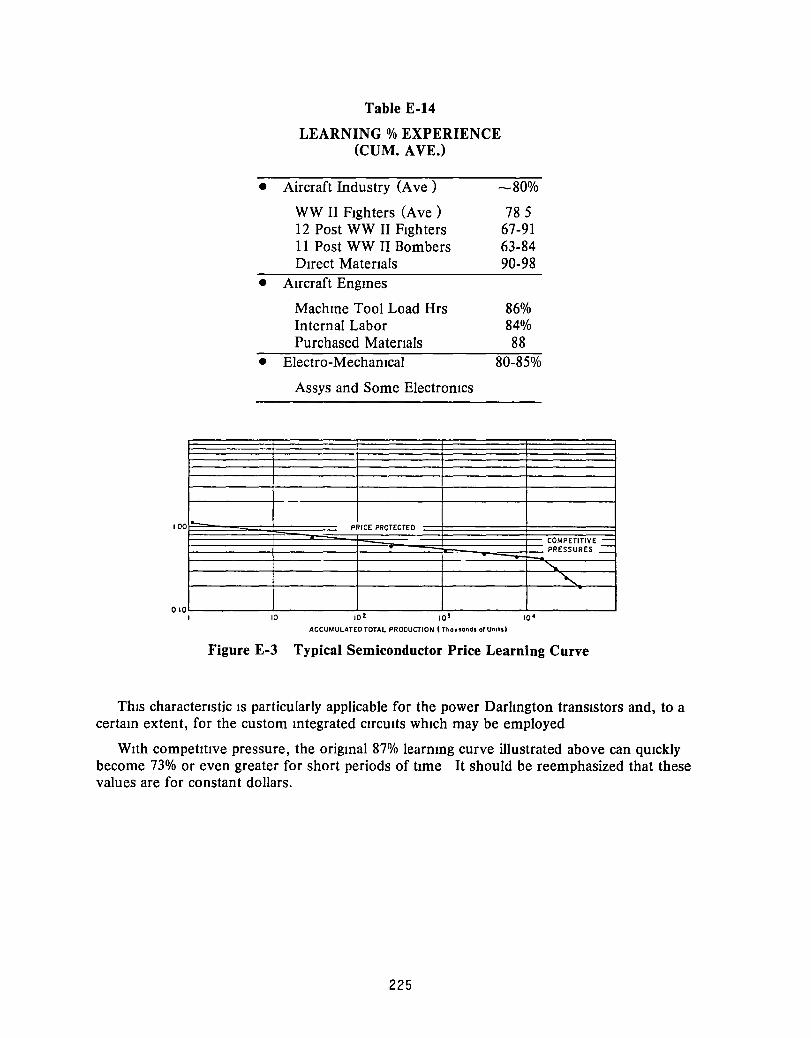
100 1--
010 I
Table E-14
LEARNING % EXPERIENCE (CUM. AVE.)
• Aircraft Industry (Ave) -80%
WW II FIghters (Ave) 785 12 Post WW II FIghters 67-91 11 Post WW II Bombers 63-84 DIrect Matenals 90-98
• AIrcraft Engmes
Machme Tool Load Hrs 86% Internal Labor 84% Purchased MaterIals 88
• Electro-MechanIcal 80-85%
Assys and Some ElectronIcs
PRICE PROTECTED
COMPETITIVE = PRESSURES _
~
" 10 10'
ACCUMULATED TOTAL PROOUCTION I Tho",ond. 0' Un,1s1
Figure E-3 Typical Semiconductor Price Learning Curve
ThIS charactenstic IS particularly applicable for the power DarlIngton transIstors and, to a certam extent, for the custom mtegrated CIrcUIts WhICh may be employed
WIth competItIve pressure, the origmal 87% learnIng curve illustrated above can qUIckly become 73% or even greater for short periods of tIme It should be reemphasized that these values are for constant dollars.
225
Section 7
DEFINITIONS
1 PropulsIon System - the aggregation of all components WhICh comprIse the power traIn plus accessory drIves and auxlharIes, wIth the sIngle exceptIOn of electrochemIcal storage batterIes
2. AC Controller - the subsystem as comprIsed of the power Inverter and ItS associated control electronIcs
3. Power Inverter - the six-transIstor Inverter wIth associated aUXIlIary components
4 Power Inverter Assembly - as referenced to the hardware Itself
5 Control Card - one of the printed CIrCUIt (p c ) boards In the control electronIcs assembly
6 Control ElectronIcs - the p c boards and associated components that control the power Inverter
7 Control ElectronIcs Assembly - as referenced to the hardware Itself
8. Life Cycle Cost - the cost per kIlometer (mIle) of mass produced hardware over ItS operatIng lIfe Factors enterIng Into thIS cost Include but are not necessarIly lImIted to the folloWIng
• FIrst cost determIned and based on projected productIOn rates of 10,000 and 100,000 per year
• OperatIng lIfetIme of 100,000 cycles of SAE 1227a, Schedule D drIVIng cycle (approxI-mately 3,500 hours)
• repaIr and/or replacement costs over the lIfetime perIod
• depreCiation and/or salvage value
• energy costs dIrectly attrIbutable to productIOn hardware weIght
• warranty costs
9 EngIneerIng Model - an Integrally assembled, representatively packaged UnIt WhICh phYSIcally resembles a proposed productIOn model In form and functIOn and IS fully responSIve to ItS operatIng requIrements and speCIficatIOns (EngIneerIng model deSIgn and testIng IS predIcated on conductIng comprehensIve performance testIng and the evaluation of all Input/output Interface characterIstics, In SItU, under controlled condItions
10 ProductIOn Model - a mass produced umt assembled and fabrIcated USIng the most cost effective technIques pOSSIble and meetIng all speCIficatIOns and reqUirements
11 SIgnal ConventIOns -
When dISCUSSIng SIgnals, the follOWIng conventions apply
a. SIgnal names wIll be shown In capItal letters, e.g, ACCELERATE*. A SIgnal name generally refers to the condItIOn IndIcated by ItS active or most pOSItive state For an analog SIgnal, the active state is the most pOSItive voltage, I.e., ACCELERATE* = + 10 volts IndIcates full acceleratIOn For a dIgItal SIgnal, the active state would be a lOgIC '1' or + 15 volts, I.e, ACe = + 15 volts indIcates acceleratIOn LOgIC '1' wIll hereafter be referred to as '1' and lOgIC '0' as '0'
226

b. An asterIsk (*) after an analog sIgnal name Indicates a command as opposed to a feedback signal, ie., IREAL * IS the real current command, whereas IREAL IS the real current feedback
c A slash (/) before a digItal sIgnal name indicates negation, i e., IBRK means that the active (' 1') state indicates "not brake," or conversely, the Inactive ('0') state Indicates "brake."
d The letter (D) after a sIgnal name indicates the version of the signal which IS output-buffered for external monitorIng purposes (diagnostics).
e. Reference locations on the schematic under diSCUSSion wIll be shown In square brackets ([]) and refer to reference marks on the left Side and top edge of the schematic.
f A signal name enclosed In a pair of vertical lInes (II) means 'the absolute value of' or magnItude of that signal, I.e., III Indicates the absolute value of I.
227

Section 8
REFERENCES
1 A B Plunkett and G B Khman, "Electnc VehIcle AC Dnve Development," SAE Paper 800061
2 A B. Plunkett and D L PIette, "Inverter-InductIOn Motor Dnve for TransIt Cars," IEEE TransactIOns on Industry ApplicatIOns IA-13 (1), January/February 1977, pp 26-37
3 PM Espelage, F G Turnbull, and J Chiera, "DC-to-AC Inverter and HIgh-Speed Induction Motor Fmal Report," S-69-1037, October 18, 1968, DOA, MERDC Contract DA-44-009-AMC-1820(T)
4 G B Khman and A.B Plunkett, "Development of a ModulatIon Strategy for a PWM Inverter Dnve," lAS Conference Record of the 10th Meetmg, October 1975
5. H C.J. Dejong, AC Motor Design wah ConventIOnal and Converter Power Supplies, Oxford UnIVersIty Press, 1976
6 H J. BoenIg, "OptImIzatIon of MagnetIc Matenals UtIlizatIOn m SemiconductorCommutated Electnc Machmes," UnIVersIty of Wisconsm Doctoral DIssertatIon m EE, UnIVersIty MIcrofilms Inc, Ann Arbor, MIchIgan, 1971
7 J A Chiera, L Coffman, J.F. Haupt, and L Ishler, "AC Electnc Wheel DesIgn Study FInal Report," February 26,1971, DOA, MERDC Contract DAAK02-70-C-0600
8. General Electnc Company, "Near-Term Elctnc VehIcle Phase II Fmal Report," March 28, 1980, DOE Contract No DE-AC03-76CS51294
9 G B KlIman and A B Plunkett, "Development of a ModulatIOn Strategy for a PWM Inverter Dnve," IEEE Transactions on Industry ApplIcatIons, Vol lA-IS, No 1, January/February 1979
10 A.B Plunkett, "A Current-Controlled PWM TransIstor Inverter Drive," Conference Record 1979 IEEE Industry ApplIcatIons SocIety Annual Meetmg, October 1979
11. GA. Kaufman and A B Plunkett, "A HIgh-Performance Torque Controller Usmg a Voltage Source Inverter and InductIon Machme," Conference Record 1981 IEEE Industry ApplIcatIOns Society Annual Meetmg, October 1981
12 WE RIppel, "Optimizing Boost Chopper Charger DesIgn," Proceedmgs of Powercon 6, May 1979
13. Cornell-Dubilier Electric Corporation, Class 201.87, Type FAH specIficatIon sheets
14 A B Plunkett, "Direct Flux and Torque RegulatIon m a PWM Inverter - InductIOn Motor Dnve," IEEE TransactIons on Industry ApplIcatIons, Vol IA-13, No.2, March/ Apnl 1977.
15. G.A. Kaufman and A.B Plunkett, "Steady-State Performance of a Voltage Source Inverter Synchronous Machine Drive System," Conference Record 1981 IEEE Industry ApplIcatIOns Society Annual Meetmg, October 1981
16. J. Franz, "Apparatus for Regulating MagnetIc Flux m an AC Machme," US Patent No 4,011,489 assigned to the General Electnc Company
17. T A. Lipo, D.W. Novotny, A.B. Plunkett and V.R Stefanovlc, "Dynamics and Control of AC Drives," Course notes, Univ. of Wisconsin Extension, November 3-5, 1976.
228

18 A. Schonung and D. Stemmler, "StatIc Frequency Changers wIth Subharmomc Control 10 COnjunctIon wIth ReversIble VarIable Speed AC DrIves," The Brown-Boven RevIew, pp 555-577 Aug ISept 1974
19. A AbbondantI, J Zubek and C J. Nordby, "Pulse WIdth Modulated Inverter Motor DrIves wIth Improved ModulatIOn," Conference Record 1974 IEEE Industry ApplIcatIons SocIety Annual Meetmg, October 1974
20 Von Konrad Hemtze, Hermann Tappemer and Manfred Welbeizahl, "Pulswechselrichter zur Drehzahlsteuerung von Asynchronmaschinen," S,emens ReVIew, Vol 45, No 3, p 154, 1971
21 K P PhIllIps, "Current Source Converter for AC Motor DrIves," IEEE PublIcatIOn 71-CI-IGA, Con! Rec. 1971 IGA 6th Annu. Meet. pp 385-392, Oct. 18-21, 1971.
22. E P Cornell and T A. LIPO, "Modeling and DesIgn of Controlled Current Induction Motor DrIve systems," Con/. Rec. IEEE-lAS 1975 10th Annu Meet., Sept. 28-0ct. 2, 1975.
23 A B Plunkett, J D. D' Atre and T.A. LIPO, "Synchronous Control of a StatIc AC InductIon Motor DrIve," Con! Rec 1977 lAS Annu. Meet., p 609, Oct 1977
24. W McMurray, "OptImum Snubbers for Power SemIconductors," Conference Record 1971 IEEE Industry AppizcatlOns SocIety Annual Meetmg, October 1971
25. "A Study of Flywheel Energy Storage for Urban TranSIt VehIcles," 16 September 1977, General ElectrIc Report SRD-77 -121, U S Department of TransportatIon, Contract DOT -UT -60096T
26 "RegeneratIve Flywheel Energy Storage System, Volume III LIfe Cycle and Cost Benefit Analyses of a Battery - Flywheel ElectrIc Car," June 27, 1980, General ElectrIc Report SRD-79-148-3, US Department of Energy under subcontract No. 8990503 from Lawrence LIvermore LaboratOrIes
27 Grant, Ireson, and Leavenworth, Engmeenng Economy, 6th edItIon, p 72
28. L L. LIston and C A AIken, "Cost of Ownmg and Operatmg an AutomobIle 1976," US. Department of TransportatIOn, Federal HIghway AdmmIstratIOn.
29 B D. Bedford and R G Hoft, Prmclples of Inverter CirCUits, John WIley and Sons, NY., 1964
229

1 Report No I 2 Government Accession No 3 RecIpient's Catalog No
NASA CR-167978 4 Title and Subtitle 5 Report Date
September 1982 Improved Transistorized ac Motor Controller For Battery Powered 6 Performing Organization Code
Urban Electric Passenger Vehicles 778-36-06
7 Author(s) 8 Performing Organization Report No
Steven C. Peak SR0-81-088
10 Work Unit No
9 Performing Organization Name and Address General Electric Company
11 Contract or Grant No Power Electronics Laboratory Corporate Research and Development DEN 3-59 Schenectady, New York 12345 13 Type of Report and Period Covered
12 Sponsoring Agency Name and Address Contractor Report U. S. Department of Energy
14 Sponsoring Agency ~ Report No. Office of Vehicle and Engine R&D Washington, D. C. 20585 OOE/NASA/0059-1
15 Supplementary Notes
Final Report. Prepared under Interagency Agreement DE-AIOl-77CS51044. ProJect Manager, F. Gourash, Transportation Propulsion Division, NASA Lewis Research Center, Cleveland, Ohio 44135.
16 Abstract
An improved ac motor controller for an induction motor electric vehicle drive system was designed, fabricated, tested, evaluated and cost analyzed. A vehicle performance analysis was done to establish the vehicle tractive effort-speed requirements. These requirements were then converted into a set of ac motor and ac controller requirements. The power inverter is a three-phase bridge using General Electric power Darlington transistors. The induction motor is a General Electric deSign optimized for use with an inverter power source. The drive system has a constant torque output to base motor speed and a constant horsepower output to maximum speed. A gear 'shifting transmission is not required. The ac controller was scaled from the base 20 hp (41 bp peak) at 108 volts dc to an expanded horsepower and battery voltage range. Motor reversal was accomplished by electronic reversal of the inverter phase sequence. The ac controller can also be used as a boost chopper battery charger. The drive system was tested on a dynamometer and results are presented. The current-controlled pulse width modulation control scheme had improved motor current waveforms. The ac controller favors a higher system voltage. Suitable power transistors are becoming more readily available but are costly. however this is expected to change in the future. Recommendations for future work are made.
17 Key Words (Suggested by Author(s)) 18 Distribution Statement
Inverter, Induction motors, Power transistors, Unclassified - unlimited Pulse width modulation, Harmonics, Efficiency, ST AR Category 33 Motor controls, Life cycle cost, Electric vehicle, DOE Category UC-96 Propulsion system, Powertrain, Drivetrain
19 Security Classlf (of thiS report) 20 Security Classlf (of thiS page) 121
No of Pages 1 22
Price'
Unclassified Unclassified 240 All
• For sale by the NatIOnal Technical InformatIOn SerVice, Springfield, Virginia 22161
*USGPO 1983 - 659-094/325

End of Document
Related Documents