COFFE: Fully-Automated Transistor Sizing for FPGAs Charles Chiasson and Vaughn Betz Department of Electrical and Computer Engineering University of Toronto, Toronto, ON, Canada {charlesc,vaughn}@eecg.utoronto.ca Abstract—In this paper, we present COFFE (Circuit Optimiza- tion For FPGA Exploration), a new fully-automated transistor sizing tool for FPGAs. Automated transistor-level CAD tools are an important part of the architecture exploration flow because they provide accurate area and delay estimates of low-level FPGA circuitry, which must be obtained for each architecture. We show that modeling transistors as linear resistances and capacitances as has been done in previous FPGA transistor sizing tools is highly inaccurate for fine-grained transistor-level design in advanced process nodes. Therefore, COFFE’s transistor sizing algorithm maintains circuit non-linearities by relying exclusively on HSPICE simulations to measure delay. Area is estimated with a transistor size-based model that incorporates a number of improvements to enhance its accuracy in advanced process technologies versus prior methods. In addition to more accurate area and delay estimation, COFFE considers more layout effects than prior published work by automatically accounting for tran- sistor and wire loads, which are computed based on architectural parameters and layout area. This new FPGA transistor sizing tool requires only several hours to produce high-quality transistor sizing results for an entire FPGA tile; a task that would normally take months of manual effort. We demonstrate COFFE’s utility in FPGA architecture studies by investigating an important new architectural question at the logic-to-routing interface. I. I NTRODUCTION When developing a new chip, FPGA architects are faced with two main tasks: choosing an architecture for their FPGA and performing the transistor-level design of that architecture. Choosing an architecture is typically accomplished with archi- tecture exploration tools such as VPR [1]. By implementing benchmark circuits on a proposed FPGA, these tools allow architects to evaluate the area, delay and power impact of various architectural choices. Based on their observations, architects can then select an FPGA architecture that meets their design goals and constraints. Transistor-level design consists of selecting circuit topolo- gies for the various subcircuits that implement the chosen architecture as well as sizing the transistors of those sub- circuits. Transistor-level design is an essential precursor to the evaluation of an architecture because it provides accurate area, delay and power estimates of the underlying FPGA circuitry; these estimates are required inputs to the architecture exploration tools. Transistor sizing also provides an additional opportunity to tune the area, delay and power of an FPGA. Therefore, developing a new FPGA is an iterative process that involves performing the transistor-level design of various architectures before evaluating them through synthesis, place- ment and routing experiments. This interdependence between architecture exploration and transistor-level design necessitates automated design tools if high-quality results are to be ob- tained in reasonable amounts of time. In this paper, we de- scribe COFFE (Circuit Optimization For FPGA Exploration), a fully-automated transistor sizing tool for FPGAs that enables the design flow detailed above by providing area, delay and power estimates of properly sized FPGA circuitry. COFFE also enables design exploration of FPGA circuitry, of which we give an example in Section VIII. Transistor sizing for custom circuits is a well-studied prob- lem that consists of improving a circuit’s performance by increasing the sizes of its transistors. This optimization prob- lem is usually formulated in one of three ways: 1) minimize some function of area and delay, 2) minimize area subject to a delay constraint or 3) minimize delay subject to an area constraint. In [2], it was shown that modeling transistors as linear resistances and capacitances and calculating the delay of the resulting RC circuits with the Elmore [3] or the Penfield-Rubinstein [4] delay model allows the transistor sizing problem to be formulated as a convex optimization problem, which guarantees that any local minimum is the global minimum. With this useful property, [2] develops TILOS, a transistor sizing tool for custom circuits based on a heuristic method that iteratively identifies a circuit’s critical path and increases transistor sizes on that path until all timing constraints are met. Despite the convexity of the problem, TILOS’s heuristic is such that it can terminate with a sub- optimal solution. Algorithms guaranteeing the optimal solution have subsequently been proposed [5]–[7] but these algorithms, along with TILOS, all suffer from their reliance on linear device models and the Elmore delay, which have long been known to be inaccurate [8], [9]. To enhance accuracy, at the cost of increased computational complexity, some transistor sizing algorithms have turned towards time-domain simulation to obtain delay estimates [10], [11]. The programmability of FPGAs adds unique features to the transistor sizing problem that Kuon and Rose tackle with an FPGA-specific transistor sizing tool [12]. Their two-phased algorithm consists of an exploratory phase that utilizes linear device models and a TILOS-like transistor sizing heuristic followed by an HSPICE-based fine-tuning phase that adjusts the transistor sizes to account for the inaccuracies of linear models. In [13], Smith et al. present a method that enables the rapid and concurrent optimization of high-level architecture parameters and transistor sizes for FPGAs through the use of analytic architecture models, linear device models and a con- vex optimization-based transistor sizing algorithm. They show that this concurrent optimization can have a significant im- pact on architectural conclusions versus separate optimization. COFFE differs from both [12] and [13] because it completely avoids the use of linear models and makes other modeling improvements which are necessary for FPGAs in advanced process nodes. Specifically, our contributions include:

Welcome message from author
This document is posted to help you gain knowledge. Please leave a comment to let me know what you think about it! Share it to your friends and learn new things together.
Transcript
COFFE: Fully-Automated Transistor Sizing for FPGAsCharles Chiasson and Vaughn Betz
Department of Electrical and Computer EngineeringUniversity of Toronto, Toronto, ON, Canadacharlesc,[email protected]
Abstract—In this paper, we present COFFE (Circuit Optimiza-tion For FPGA Exploration), a new fully-automated transistorsizing tool for FPGAs. Automated transistor-level CAD tools arean important part of the architecture exploration flow becausethey provide accurate area and delay estimates of low-levelFPGA circuitry, which must be obtained for each architecture.We show that modeling transistors as linear resistances andcapacitances as has been done in previous FPGA transistor sizingtools is highly inaccurate for fine-grained transistor-level designin advanced process nodes. Therefore, COFFE’s transistor sizingalgorithm maintains circuit non-linearities by relying exclusivelyon HSPICE simulations to measure delay. Area is estimatedwith a transistor size-based model that incorporates a numberof improvements to enhance its accuracy in advanced processtechnologies versus prior methods. In addition to more accuratearea and delay estimation, COFFE considers more layout effectsthan prior published work by automatically accounting for tran-sistor and wire loads, which are computed based on architecturalparameters and layout area. This new FPGA transistor sizingtool requires only several hours to produce high-quality transistorsizing results for an entire FPGA tile; a task that would normallytake months of manual effort. We demonstrate COFFE’s utilityin FPGA architecture studies by investigating an important newarchitectural question at the logic-to-routing interface.
I. INTRODUCTION
When developing a new chip, FPGA architects are facedwith two main tasks: choosing an architecture for their FPGAand performing the transistor-level design of that architecture.Choosing an architecture is typically accomplished with archi-tecture exploration tools such as VPR [1]. By implementingbenchmark circuits on a proposed FPGA, these tools allowarchitects to evaluate the area, delay and power impact ofvarious architectural choices. Based on their observations,architects can then select an FPGA architecture that meetstheir design goals and constraints.
Transistor-level design consists of selecting circuit topolo-gies for the various subcircuits that implement the chosenarchitecture as well as sizing the transistors of those sub-circuits. Transistor-level design is an essential precursor tothe evaluation of an architecture because it provides accuratearea, delay and power estimates of the underlying FPGAcircuitry; these estimates are required inputs to the architectureexploration tools. Transistor sizing also provides an additionalopportunity to tune the area, delay and power of an FPGA.Therefore, developing a new FPGA is an iterative processthat involves performing the transistor-level design of variousarchitectures before evaluating them through synthesis, place-ment and routing experiments. This interdependence betweenarchitecture exploration and transistor-level design necessitatesautomated design tools if high-quality results are to be ob-tained in reasonable amounts of time. In this paper, we de-scribe COFFE (Circuit Optimization For FPGA Exploration),
a fully-automated transistor sizing tool for FPGAs that enablesthe design flow detailed above by providing area, delay andpower estimates of properly sized FPGA circuitry. COFFEalso enables design exploration of FPGA circuitry, of whichwe give an example in Section VIII.
Transistor sizing for custom circuits is a well-studied prob-lem that consists of improving a circuit’s performance byincreasing the sizes of its transistors. This optimization prob-lem is usually formulated in one of three ways: 1) minimizesome function of area and delay, 2) minimize area subjectto a delay constraint or 3) minimize delay subject to anarea constraint. In [2], it was shown that modeling transistorsas linear resistances and capacitances and calculating thedelay of the resulting RC circuits with the Elmore [3] orthe Penfield-Rubinstein [4] delay model allows the transistorsizing problem to be formulated as a convex optimizationproblem, which guarantees that any local minimum is theglobal minimum. With this useful property, [2] developsTILOS, a transistor sizing tool for custom circuits based ona heuristic method that iteratively identifies a circuit’s criticalpath and increases transistor sizes on that path until all timingconstraints are met. Despite the convexity of the problem,TILOS’s heuristic is such that it can terminate with a sub-optimal solution. Algorithms guaranteeing the optimal solutionhave subsequently been proposed [5]–[7] but these algorithms,along with TILOS, all suffer from their reliance on lineardevice models and the Elmore delay, which have long beenknown to be inaccurate [8], [9]. To enhance accuracy, at thecost of increased computational complexity, some transistorsizing algorithms have turned towards time-domain simulationto obtain delay estimates [10], [11].
The programmability of FPGAs adds unique features to thetransistor sizing problem that Kuon and Rose tackle with anFPGA-specific transistor sizing tool [12]. Their two-phasedalgorithm consists of an exploratory phase that utilizes lineardevice models and a TILOS-like transistor sizing heuristicfollowed by an HSPICE-based fine-tuning phase that adjuststhe transistor sizes to account for the inaccuracies of linearmodels. In [13], Smith et al. present a method that enables therapid and concurrent optimization of high-level architectureparameters and transistor sizes for FPGAs through the use ofanalytic architecture models, linear device models and a con-vex optimization-based transistor sizing algorithm. They showthat this concurrent optimization can have a significant im-pact on architectural conclusions versus separate optimization.COFFE differs from both [12] and [13] because it completelyavoids the use of linear models and makes other modelingimprovements which are necessary for FPGAs in advancedprocess nodes. Specifically, our contributions include:
LC
SBCB
FPGA Tile
Routing Channel
CB
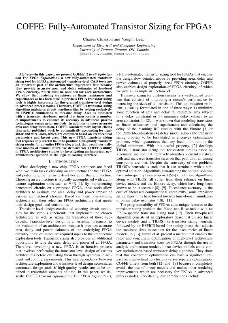
Fig. 1: Tile-based FPGA.
• An FPGA transistor sizing tool1 that sizes the transistorsof an entire FPGA tile by intelligently searching the designspace while modeling all circuit non-linearity. We showin Section III that this full non-linear modeling is key.
• New and more accurate area and wire load models.• An analysis of the effect of wire loading at the interface
between logic clusters and routing channels.
II. PROBLEM FORMULATION AND DESIGN FLOW
A. FPGA ArchitectureAn FPGA is composed of an array of tiles interconnected
by programmable routing channels (Fig. 1). Each tile consistsof a logic cluster (LC), a connection block (CB) and a switchblock (SB). The logic cluster implements a small amount oflogic and local routing while the connection block and switchblock provide connectivity between the logic cluster and therouting channels. The switch block also provides connectivitybetween wires within the routing channels.
Fig. 2 shows the tile architecture that COFFE supports inits designs and Table I lists the architecture parameters thatCOFFE expects as inputs. Parameters listed in the top portionof Table I are commonly used in FPGA research [1], [14].Parameters listed in the bottom portion are new and helpCOFFE describe a more flexible basic logic element (BLE)than the commonly used academic BLE [1]. The COFFEBLE still consists of a K-input lookup table (LUT) andflip-flop (FF) but has more flexible ways to use the LUTand FF simultaneously. The Rfb parameter allows optionallyincluding a register feedback multiplexer (MUX-A in Fig. 2)on a LUT input. Each input has an Rfb parameter. The FF canbe designed to accept its input either directly from the LUToutput or from either the LUT output or a BLE input (throughMUX-B) with the Rsel parameter. COFFE’s BLEs supportvariable numbers of local feedback and general routing outputswhich are specified by the Ofb and Or parameters respectively.All BLE outputs can be driven by either the LUT output or theFF output (MUX-C and MUX-D). These extra 2:1 MUXes canpotentially help improve density and speed and are similar tothe ones used in Stratix [15]. COFFE currently only supportsone wire segment length (L) and uses directional, single-driverrouting wires [16].
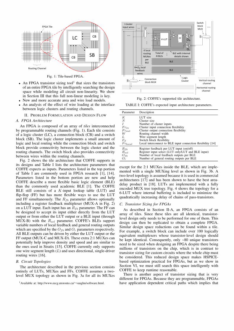
B. Circuit TopologiesThe architecture described in the previous section consists
entirely of LUTs, MUXes and FFs. COFFE assumes a two-level MUX topology as shown in Fig. 3a for all its MUXes
1Available at: http://www.eecg.utoronto.ca/∼vaughn/software.html.
K-LUT FF
BLE with internal details shown
AB C
D
Logic Cluster
BLE
BLE
Total of N BLEs
Switch block MUX
Vertical routing channel
N•Ofb local feedback
wires
I cluster input wires
K local routing MUXes
per BLE
Connection block MUX
Ofb
Or
Horizontal routing channel
Fig. 2: COFFE’s supported tile architecture.
TABLE I: COFFE’s expected input architecture parameters.
Parameter Description
K LUT sizeN Cluster sizeI Number of cluster inputsFcin Cluster input connection flexibilityFcout Cluster output connection flexibilityW Routing channel widthL Wire segment lengthFS Switch block flexibilityFclocal Local interconnect to BLE input connection flexibility [14]
Rfb Register feedback per LUT input (on/off)Rsel Register input select (LUT only/LUT and BLE input)Ofb Number of local feedback outputs per BLEOr Number of general routing outputs per BLE
except for the 2:1 MUXes inside the BLE, which are imple-mented with a single MUXing level as shown in Fig. 3b. Atwo-level topology is assumed because it is used in commercialarchitectures [17] and has been shown to have the best area-delay product in [18]. LUTs are implemented with a fullyencoded MUX tree topology. Fig. 4 shows the topology for a6-LUT where internal buffering is included to minimize thequadratically increasing delay of chains of pass-transistors.
C. Transistor Sizing for FPGAsAs described in Section II-A, an FPGA consists of an
array of tiles. Since these tiles are all identical, transistor-level design only needs to be performed for one of them. Thisdesign can then be replicated to obtain a complete FPGA.Similar design space reductions can be found within a tile.For example, a switch block can include over 100 logicallyequivalent multiplexers whose transistor-level design shouldbe kept identical. Consequently, only ~80 unique transistorsneed to be sized when designing an FPGA despite there beingmillions of transistors on the chip, which is in contrast totransistor sizing for custom circuits where the whole chip mustbe considered. This reduced design space makes HSPICE-based optimization practical for FPGAs, but as we show inSection VI, we must still search this space intelligently withCOFFE to keep runtime reasonable.
There is another aspect of transistor sizing that is verydifferent for FPGAs. Because they are programmable, FPGAshave application dependent critical paths which implies that
Level-restorer
lvl1
lvl2
buf1
buf2
out
SRAM cell
lvl1
2-stage buffer2-level MUX
(a)
Level-restorer
lvl1
buf1buf2
out
SRAM cell
2-stage buffer2:1 MUX
(b)
Fig. 3: a) Two-level MUX topology. b) 2:1 MUX topology.
IN_A IN_B IN_C IN_D IN_E IN_F
SRAM
LUT input drivers
Fig. 4: Fully-encoded MUX tree 6-LUT topology with internalbuffering (partial view).
at design time, there is no clear critical path to optimize fordelay. To deal with this issue, [12] optimizes a representativepath that contains one of each type of FPGA subcircuit (LUTs,MUXes, etc.). Delay is taken as a weighted sum of the delayof each subcircuit and the weighting scheme is chosen basedon the frequency with which each subcircuit was found on thecritical paths of placed and routed benchmark circuits. In [19],the lack of a critical path is confronted by simply optimizingeach subcircuit individually. As we will describe in more detailin Section VI, COFFE can be configured to use either of thesetwo approaches.
D. Design Flow
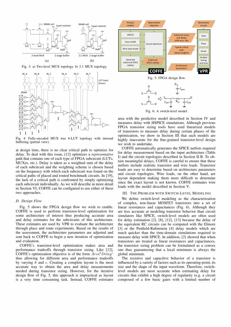
Fig. 5 shows the FPGA design flow we wish to enable.COFFE is used to perform transistor-level optimization forsome architecture of interest thus producing accurate areaand delay estimates for the subcircuits of this architecture.These estimates are used by VPR to evaluate the architecturethrough place and route experiments. Based on the results ofthe assessment, the architecture parameters are adjusted andsent back to COFFE to begin a new iteration of optimizationand evaluation.
COFFE’s transistor-level optimization makes area andperformance tradeoffs through transistor sizing. Like [12],COFFE’s optimization objective is of the form AreabDelayc
thus allowing for different area and performance tradeoffsby varying b and c. Creating a complete layout is the mostaccurate way to obtain the area and delay measurementsneeded during transistor sizing. However, for the iterativedesign flow of Fig. 5, this approach is impractical as layoutis a very time consuming task. Instead, COFFE estimates
Wire load model
Circuit OptimizerArea model
HSPICE
Subcircuit SPICE netlists
Generate subcircuit SPICE
netlists
COFFE
Optimization objective
Process models
Subcircuit areas and delays
(VPR arch. file)
Typical critical path
(delay weights)
Architecture parameters
VPR
Pack
Place
Route
Benchmark circuits
Analyze timing
and area
Fig. 5: FPGA design flow.
Cdiff CdiffReq
Cgate
S D
G
S D
GS D
G
Fig. 6: A switch-level model.
area with the predictive model described in Section IV andmeasures delay with HSPICE simulations. Although previousFPGA transistor sizing tools have used linearized modelsof transistors to measure delay during certain phases of theoptimization, we show in Section III that such models arehighly inaccurate for the fine-grained transistor-level designwe wish to undertake.
COFFE automatically generates the SPICE netlists requiredfor delay measurement based on the input architecture (TableI) and the circuit topologies described in Section II-B. To ob-tain meaningful delays, COFFE is careful to ensure that thesenetlists include realistic transistor and wire loads. Transistorloads are easy to determine based on architecture parametersand circuit topologies. Wire loads, on the other hand, arelayout dependent making them more difficult to determinesince the exact layout is not known. COFFE estimates wireloads with the model described in Section V.
III. THE PROBLEM WITH SWITCH-LEVEL MODELING
We define switch-level modeling as the characterizationof complex, non-linear MOSFET transistors into a set oflinear resistances and capacitances (Fig. 6). Although theyare less accurate at modeling transistor behavior than circuitsimulators like SPICE, switch-level models are often usedfor delay estimation [2], [8], [12], [13] because the delay ofthe equivalent RC circuits can be computed with the Elmore[3] or the Penfield-Rubinstein [4] delay models which aremuch quicker than the time-domain simulations required tomeasure delay with SPICE. In addition, [2] showed that whentransistors are treated as linear resistances and capacitances,the transistor sizing problem can be formulated as a convexone thus guaranteeing that a local minimum is always theglobal minimum.
The resistive and capacitive behavior of a transistor isinfluenced by a variety of factors such as its operating-point, itssize and the shape of the input waveform. Therefore, switch-level models are most accurate when estimating delay forcircuits that exhibit a high degree of regularity (e.g. a circuitcomposed of a few basic gates with a limited number of
CloadCloadCloadCloadCload
trisetfall
(a)
Cload
trise
(b)
Cload
tfall
(c)
Cload
trise
(d)
Cload
tfall
(e)
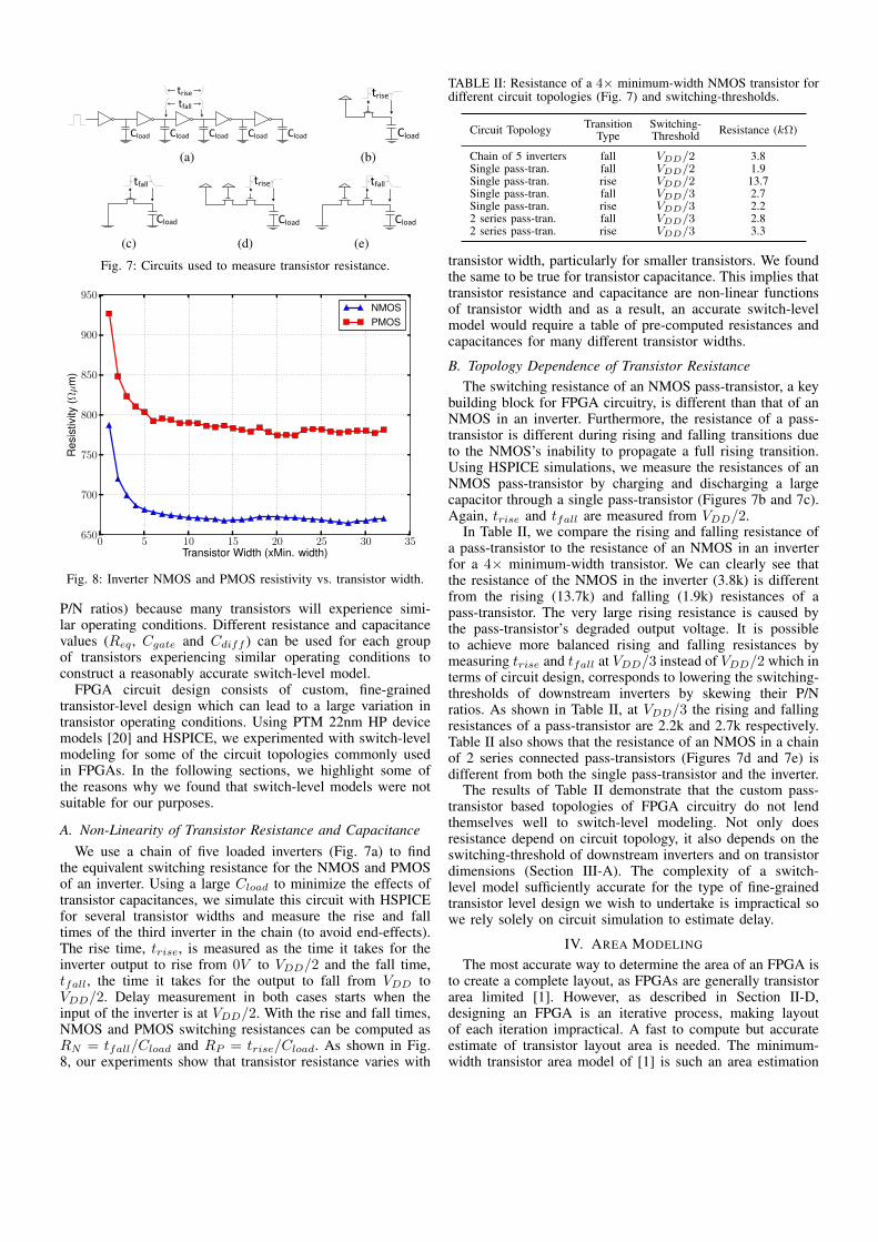
Fig. 7: Circuits used to measure transistor resistance.
0 5 10 15 20 25 30 35Transistor Width (xMin. width)
650
700
750
800
850
900
950
Res
istiv
ity(Ωµ
m)
NMOSPMOS
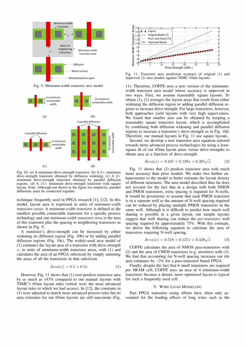
Fig. 8: Inverter NMOS and PMOS resistivity vs. transistor width.
P/N ratios) because many transistors will experience simi-lar operating conditions. Different resistance and capacitancevalues (Req , Cgate and Cdiff ) can be used for each groupof transistors experiencing similar operating conditions toconstruct a reasonably accurate switch-level model.
FPGA circuit design consists of custom, fine-grainedtransistor-level design which can lead to a large variation intransistor operating conditions. Using PTM 22nm HP devicemodels [20] and HSPICE, we experimented with switch-levelmodeling for some of the circuit topologies commonly usedin FPGAs. In the following sections, we highlight some ofthe reasons why we found that switch-level models were notsuitable for our purposes.
A. Non-Linearity of Transistor Resistance and CapacitanceWe use a chain of five loaded inverters (Fig. 7a) to find
the equivalent switching resistance for the NMOS and PMOSof an inverter. Using a large Cload to minimize the effects oftransistor capacitances, we simulate this circuit with HSPICEfor several transistor widths and measure the rise and falltimes of the third inverter in the chain (to avoid end-effects).The rise time, trise, is measured as the time it takes for theinverter output to rise from 0V to VDD/2 and the fall time,tfall, the time it takes for the output to fall from VDD toVDD/2. Delay measurement in both cases starts when theinput of the inverter is at VDD/2. With the rise and fall times,NMOS and PMOS switching resistances can be computed asRN = tfall/Cload and RP = trise/Cload. As shown in Fig.8, our experiments show that transistor resistance varies with
TABLE II: Resistance of a 4× minimum-width NMOS transistor fordifferent circuit topologies (Fig. 7) and switching-thresholds.
Circuit Topology Transition Switching- Resistance (kΩ)Type Threshold
Chain of 5 inverters fall VDD/2 3.8Single pass-tran. fall VDD/2 1.9Single pass-tran. rise VDD/2 13.7Single pass-tran. fall VDD/3 2.7Single pass-tran. rise VDD/3 2.22 series pass-tran. fall VDD/3 2.82 series pass-tran. rise VDD/3 3.3
transistor width, particularly for smaller transistors. We foundthe same to be true for transistor capacitance. This implies thattransistor resistance and capacitance are non-linear functionsof transistor width and as a result, an accurate switch-levelmodel would require a table of pre-computed resistances andcapacitances for many different transistor widths.
B. Topology Dependence of Transistor ResistanceThe switching resistance of an NMOS pass-transistor, a key
building block for FPGA circuitry, is different than that of anNMOS in an inverter. Furthermore, the resistance of a pass-transistor is different during rising and falling transitions dueto the NMOS’s inability to propagate a full rising transition.Using HSPICE simulations, we measure the resistances of anNMOS pass-transistor by charging and discharging a largecapacitor through a single pass-transistor (Figures 7b and 7c).Again, trise and tfall are measured from VDD/2.
In Table II, we compare the rising and falling resistance ofa pass-transistor to the resistance of an NMOS in an inverterfor a 4× minimum-width transistor. We can clearly see thatthe resistance of the NMOS in the inverter (3.8k) is differentfrom the rising (13.7k) and falling (1.9k) resistances of apass-transistor. The very large rising resistance is caused bythe pass-transistor’s degraded output voltage. It is possibleto achieve more balanced rising and falling resistances bymeasuring trise and tfall at VDD/3 instead of VDD/2 which interms of circuit design, corresponds to lowering the switching-thresholds of downstream inverters by skewing their P/Nratios. As shown in Table II, at VDD/3 the rising and fallingresistances of a pass-transistor are 2.2k and 2.7k respectively.Table II also shows that the resistance of an NMOS in a chainof 2 series connected pass-transistors (Figures 7d and 7e) isdifferent from both the single pass-transistor and the inverter.
The results of Table II demonstrate that the custom pass-transistor based topologies of FPGA circuitry do not lendthemselves well to switch-level modeling. Not only doesresistance depend on circuit topology, it also depends on theswitching-threshold of downstream inverters and on transistordimensions (Section III-A). The complexity of a switch-level model sufficiently accurate for the type of fine-grainedtransistor level design we wish to undertake is impractical sowe rely solely on circuit simulation to estimate delay.
IV. AREA MODELING
The most accurate way to determine the area of an FPGA isto create a complete layout, as FPGAs are generally transistorarea limited [1]. However, as described in Section II-D,designing an FPGA is an iterative process, making layoutof each iteration impractical. A fast to compute but accurateestimate of transistor layout area is needed. The minimum-width transistor area model of [1] is such an area estimation
Minimum-width transistor
Minimum-width transistor area
Space to neighboring transistors
Metal/polysilicon gate
Metal contact
Diffusion
Fig. 9: Minimum-width transistor area model.
1x minimum contactable
width
(a)
2x minimum contactable width
(b)
1x minimum contactable
width
2 parallel diffusions
(c)
5x
min
imu
m
con
tact
able
wid
th
3 parallel diffusions
(d)
Fig. 10: (a) A minimum drive-strength transistor. (b) A 2× minimumdrive-strength transistor obtained by diffusion widening. (c) A 2×minimum drive-strength transistor obtained by parallel diffusionregions. (d) A 15× minimum drive-strength transistor with squarelayout. Note: Although not shown in the figure for simplicity, paralleldiffusions must be connected together.
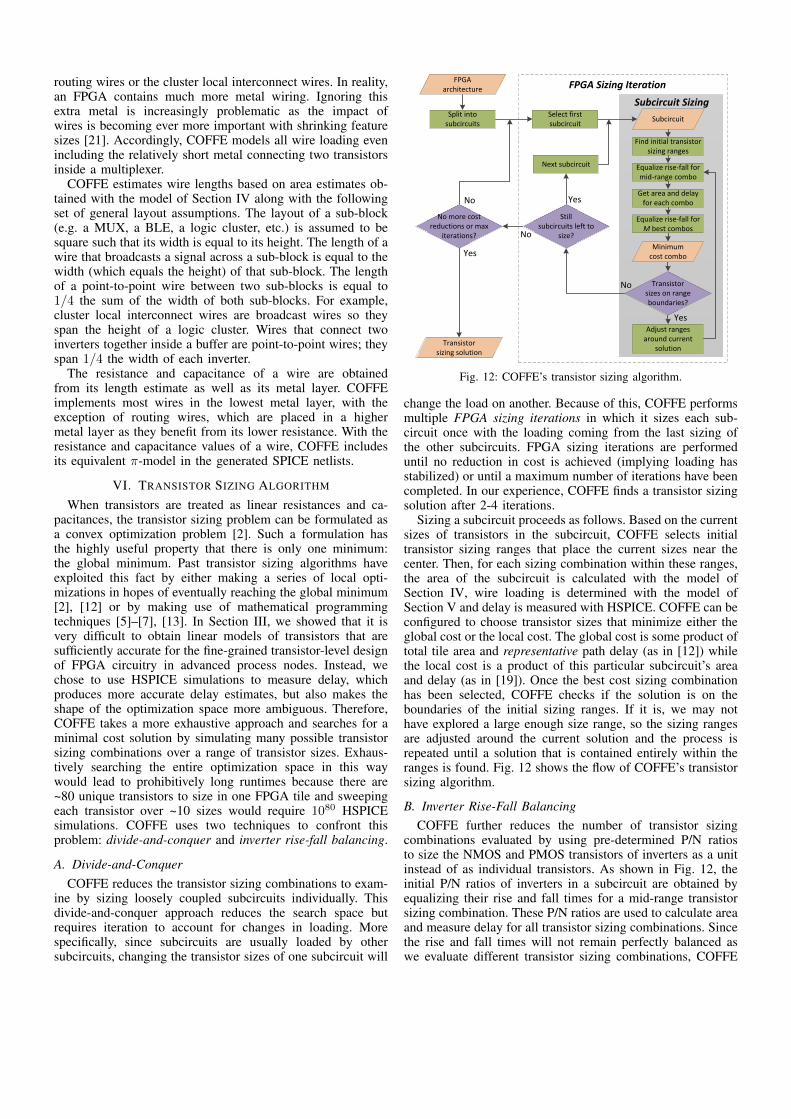
technique frequently used in FPGA research [1], [12]. In thismodel, layout area is expressed in units of minimum-widthtransistor areas. A minimum-width transistor is defined as thesmallest possible contactable transistor for a specific processtechnology and one minimum-width transistor area is the areaof this transistor plus the spacing to neighboring transistors asshown in Fig. 9.
A transistor’s drive-strength can be increased by eitherwidening its diffusion region (Fig. 10b) or by adding paralleldiffusion regions (Fig. 10c). The widely-used area model of[1] estimates the layout area of a transistor with drive-strengthx, in units of minimum-width transistor areas, with (1) andcalculates the area of an FPGA subcircuit by simply summingthe areas of all the transistors in that subcircuit.
Area(x) = 0.5 + 0.5x (1)
However, Fig. 11 shows that (1) over-predicts transistor areaby as much as 143% compared to our manual layouts withTSMC’s 65nm layout rules (which were the most advancedlayout rules to which we had access). In [12], the constants in(1) were adjusted to match more advanced process rules but itsarea estimates for our 65nm layouts are still inaccurate (Fig.
0 5 10 15 20 25 30 35Drive Strength (xMin.)
0
2
4
6
8
10
12
14
16
18
Min
imum
Wid
thTr
ansi
stor
Are
as
LayoutOriginal Model [1]Kuon and Rose [12]Improved Model
Fig. 11: Transistor area prediction accuracy of original (1) andimproved (2) area models against TSMC 65nm layouts.
11). Therefore, COFFE uses a new version of the minimum-width transistor area model whose accuracy is improved intwo ways. First, we assume reasonably square layouts. Toobtain (1), [1] averages the layout areas that result from eitherwidening the diffusion region or adding parallel diffusion re-gions to increase drive-strength. For large transistors, however,both approaches yield layouts with very high aspect-ratios.We found that smaller area can be obtained by keeping areasonably square transistor layout, which is accomplishedby combining both diffusion widening and parallel diffusionregions to increase a transistor’s drive-strength as in Fig. 10d.Therefore, our manual layouts in Fig. 11 use square layouts.
Second, we develop a new transistor area equation tailoredtowards more advanced process technologies by using a least-square fit of our 65nm layout areas versus drive-strengths toobtain area as a function of drive-strength.
Area(x) = 0.447 + 0.128x+ 0.391√x (2)
Fig. 11 shows that (2) predicts transistor area with muchmore accuracy than prior models. We make two further en-hancements to the model to better estimate the layout densityof different structures. The area model described thus far doesnot account for the fact that in a design with both NMOSand PMOS transistors, extra spacing is required for N-wells.It would be pessimistic to assume that each PMOS transistoris in a separate well as the amount of N-well spacing requiredcan be reduced by placing multiple PMOS transistors in thesame well. Although it is difficult to predict how much wellsharing is possible in a given layout, our sample layoutssuggest that well sharing can reduce the per-transistor wellspacing required by approximately 75%. With this estimate,we derive the following equation to calculate the area oftransistors requiring N-well spacing.
Area(x) = 0.518 + 0.127x+ 0.428√x (3)
COFFE calculates the area of NMOS pass-transistors with(2) and the area of CMOS transistors (e.g. inverters) with (3).We find that accounting for N-well spacing increases our tilearea estimates by ~2% for a pass-transistor based FPGA.
Finally, despite the fact that 6 small transistors are requiredper SRAM cell, COFFE uses an area of 4 minimum-widthtransistors because a denser, more optimized layout is typicalfor such a frequently used cell.
V. WIRE LOAD MODELING
Past FPGA transistor sizing efforts have often only ac-counted for the loading effects of long wires such as the
routing wires or the cluster local interconnect wires. In reality,an FPGA contains much more metal wiring. Ignoring thisextra metal is increasingly problematic as the impact ofwires is becoming ever more important with shrinking featuresizes [21]. Accordingly, COFFE models all wire loading evenincluding the relatively short metal connecting two transistorsinside a multiplexer.
COFFE estimates wire lengths based on area estimates ob-tained with the model of Section IV along with the followingset of general layout assumptions. The layout of a sub-block(e.g. a MUX, a BLE, a logic cluster, etc.) is assumed to besquare such that its width is equal to its height. The length of awire that broadcasts a signal across a sub-block is equal to thewidth (which equals the height) of that sub-block. The lengthof a point-to-point wire between two sub-blocks is equal to1/4 the sum of the width of both sub-blocks. For example,cluster local interconnect wires are broadcast wires so theyspan the height of a logic cluster. Wires that connect twoinverters together inside a buffer are point-to-point wires; theyspan 1/4 the width of each inverter.
The resistance and capacitance of a wire are obtainedfrom its length estimate as well as its metal layer. COFFEimplements most wires in the lowest metal layer, with theexception of routing wires, which are placed in a highermetal layer as they benefit from its lower resistance. With theresistance and capacitance values of a wire, COFFE includesits equivalent π-model in the generated SPICE netlists.
VI. TRANSISTOR SIZING ALGORITHM
When transistors are treated as linear resistances and ca-pacitances, the transistor sizing problem can be formulated asa convex optimization problem [2]. Such a formulation hasthe highly useful property that there is only one minimum:the global minimum. Past transistor sizing algorithms haveexploited this fact by either making a series of local opti-mizations in hopes of eventually reaching the global minimum[2], [12] or by making use of mathematical programmingtechniques [5]–[7], [13]. In Section III, we showed that it isvery difficult to obtain linear models of transistors that aresufficiently accurate for the fine-grained transistor-level designof FPGA circuitry in advanced process nodes. Instead, wechose to use HSPICE simulations to measure delay, whichproduces more accurate delay estimates, but also makes theshape of the optimization space more ambiguous. Therefore,COFFE takes a more exhaustive approach and searches for aminimal cost solution by simulating many possible transistorsizing combinations over a range of transistor sizes. Exhaus-tively searching the entire optimization space in this waywould lead to prohibitively long runtimes because there are~80 unique transistors to size in one FPGA tile and sweepingeach transistor over ~10 sizes would require 1080 HSPICEsimulations. COFFE uses two techniques to confront thisproblem: divide-and-conquer and inverter rise-fall balancing.
A. Divide-and-ConquerCOFFE reduces the transistor sizing combinations to exam-
ine by sizing loosely coupled subcircuits individually. Thisdivide-and-conquer approach reduces the search space butrequires iteration to account for changes in loading. Morespecifically, since subcircuits are usually loaded by othersubcircuits, changing the transistor sizes of one subcircuit will
Subcircuit Sizing
FPGA Sizing Iteration
Yes
No
Yes
No Yes
No
Find initial transistor sizing ranges
Transistor sizes on range boundaries?
Equalize rise-fall for mid-range combo
Get area and delay for each combo
Minimum cost combo
Subcircuit
Adjust ranges around current
solution
Equalize rise-fall for M best combos
Select first subcircuit
Split into subcircuits
Next subcircuit
Still subcircuits left to
size?
No more cost reductions or max
iterations?
Transistor sizing solution
FPGA architecture
Fig. 12: COFFE’s transistor sizing algorithm.
change the load on another. Because of this, COFFE performsmultiple FPGA sizing iterations in which it sizes each sub-circuit once with the loading coming from the last sizing ofthe other subcircuits. FPGA sizing iterations are performeduntil no reduction in cost is achieved (implying loading hasstabilized) or until a maximum number of iterations have beencompleted. In our experience, COFFE finds a transistor sizingsolution after 2-4 iterations.
Sizing a subcircuit proceeds as follows. Based on the currentsizes of transistors in the subcircuit, COFFE selects initialtransistor sizing ranges that place the current sizes near thecenter. Then, for each sizing combination within these ranges,the area of the subcircuit is calculated with the model ofSection IV, wire loading is determined with the model ofSection V and delay is measured with HSPICE. COFFE can beconfigured to choose transistor sizes that minimize either theglobal cost or the local cost. The global cost is some product oftotal tile area and representative path delay (as in [12]) whilethe local cost is a product of this particular subcircuit’s areaand delay (as in [19]). Once the best cost sizing combinationhas been selected, COFFE checks if the solution is on theboundaries of the initial sizing ranges. If it is, we may nothave explored a large enough size range, so the sizing rangesare adjusted around the current solution and the process isrepeated until a solution that is contained entirely within theranges is found. Fig. 12 shows the flow of COFFE’s transistorsizing algorithm.
B. Inverter Rise-Fall BalancingCOFFE further reduces the number of transistor sizing
combinations evaluated by using pre-determined P/N ratiosto size the NMOS and PMOS transistors of inverters as a unitinstead of as individual transistors. As shown in Fig. 12, theinitial P/N ratios of inverters in a subcircuit are obtained byequalizing their rise and fall times for a mid-range transistorsizing combination. These P/N ratios are used to calculate areaand measure delay for all transistor sizing combinations. Sincethe rise and fall times will not remain perfectly balanced aswe evaluate different transistor sizing combinations, COFFE
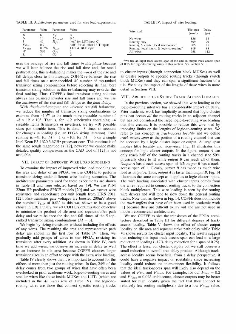
TABLE III: Architecture parameters used for wire load experiments.
Parameter Value Parameter Value
K 6 FS 3N 10 Fclocal 0.5I 40 Rfb “on” for LUT-input CFcin 0.2 “off” for all other LUT inputsFcout 0.025 Rsel LUT & BLE inputW 320 Ofb 1L 4 Or 2
uses the average of rise and fall times in this phase becausewe will later balance the rise and fall time and, for smallperturbations, this re-balancing makes the worst of the rise andfall delays close to this average. COFFE re-balances the riseand fall times on a user-specified M number of top-rankedtransistor sizing combinations before selecting its final besttransistor sizing solution as this re-balancing may re-order thefinal ranking. Thus, COFFE’s final transistor sizing solutionalways has balanced inverter rise and fall times and we usethe maximum of the rise and fall delays as the final delay.
With divide-and-conquer and inverter rise-fall balancing,we reduce the number of transistor sizing combinations toexamine from ~1080 to the much more tractable number of~3 × 12 × 104. That is, for ~12 subcircuits containing ~4sizeable items (transistors or inverters), we try ~10 possiblesizes per sizeable item. This is done ~3 times to accountfor changes in loading (i.e. an FPGA sizing iteration). Totalruntime is ~4h for M = 1 or ~10h for M = 5 on a singleIntel Xeon E5-1620 3.6GHz processor core. This runtime is ofthe same rough magnitude as [12], however we cannot makedetailed quality comparisons as the CAD tool of [12] is notavailable.
VII. IMPACT OF IMPROVED WIRE LOAD MODELING
To examine the impact of improved wire load modeling onthe area and delay of an FPGA, we use COFFE to performtransistor sizing under different wire loading scenarios. Thearchitecture parameters used for these experiments are shownin Table III and were selected based on [19]. We use PTM22nm HP predictive SPICE models [20] and we extract wireresistance and capacitance per unit length from ITRS 2011[22]. Pass-transistor gate voltages are boosted 200mV abovethe nominal VDD of 0.8V as this was shown to be a goodchoice in [19]. Finally, we set COFFE’s optimization objectiveto minimize the product of tile area and representative pathdelay and we re-balance the rise and fall times of the 5 top-ranked transistor sizing combinations (M = 5).
We begin by sizing transistors without including the effectsof any wires. The resulting tile area and representative pathdelay are shown in the first row of Table IV. Then, wegradually add groups of wires to our FPGA, re-sizing itstransistors after every addition. As shown in Table IV, eachtime we add wires, we observe an increase in delay as wellas an increase in tile area because COFFE chooses largertransistor sizes in an effort to cope with the extra wire loading.
Table IV clearly shows that it is important to account for theeffects of more than just the routing wires. In fact, 24% of thedelay comes from two groups of wires that have often beenoverlooked in prior academic work: logic-to-routing wires andsmaller wires like those inside MUXes and LUTs (which areincluded in the All wires row of Table IV). The logic-to-routing wires are those that connect specific routing tracks
TABLE IV: Impact of wire loading.
Wire load Tile area Delay(µm2) (ps)
No wires 836 58Routing only 899 79Routing & cluster local interconnect 905 85Routing, local interc. & logic-to-routinga 919 98All wires 938 112
aWe use an input track-access span of 0.5 and an output track-access spanof 0.25 for logic-to-routing wires in this section. See Section VIII.
to cluster inputs (through connection block MUXes) as wellas cluster outputs to specific routing tracks (through switchblock MUXes) and they can span a significant fraction of atile. We study the impact of the lengths of these wires in moredetail in Section VIII.
VIII. ARCHITECTURE STUDY: TRACK-ACCESS LOCALITY
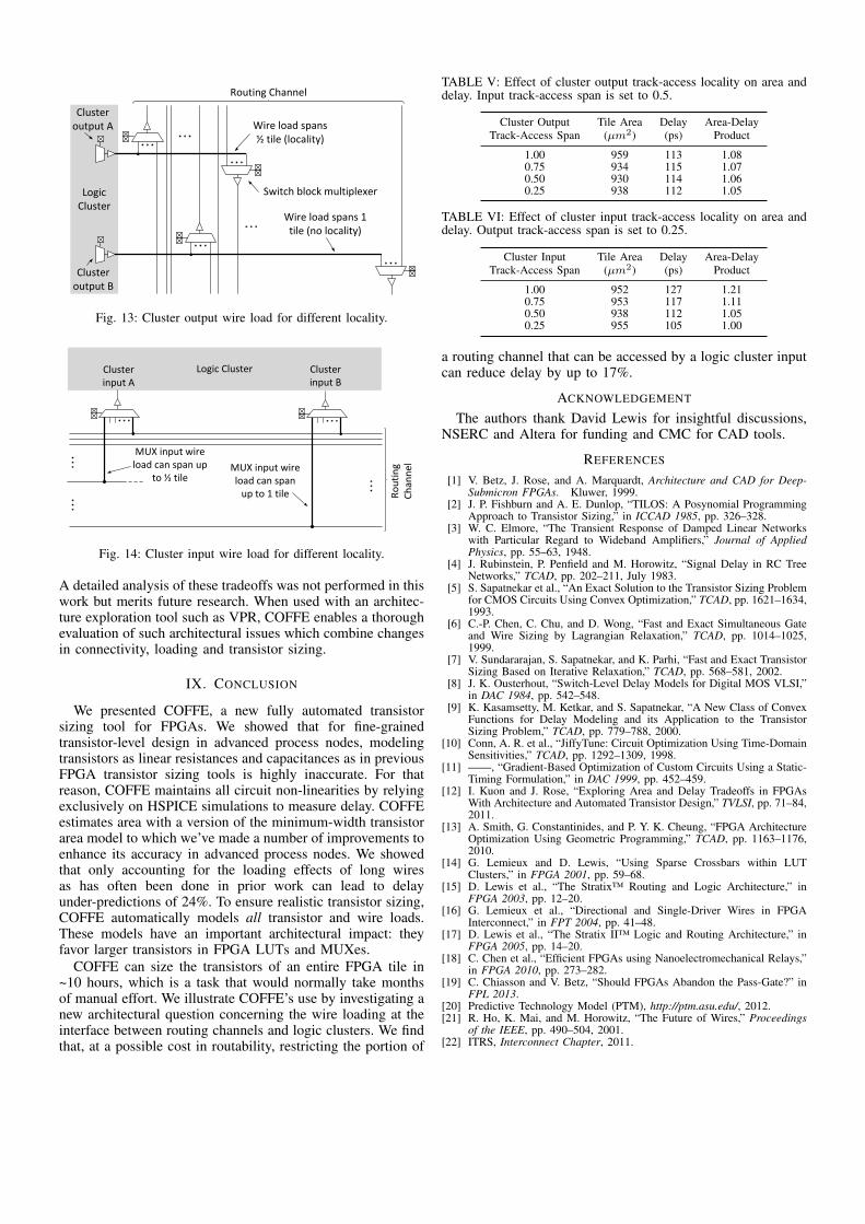
In the previous section, we showed that wire loading at thelogic-to-routing interface has a considerable impact on delay.Prior academic work has implicitly assumed that logic clusterpins can access all the routing tracks in an adjacent channelbut has not considered the large logic-to-routing wire loadingthat this creates. It is possible to reduce this wire load byimposing limits on the lengths of logic-to-routing wires. Werefer to this concept as track-access locality and we definetrack-access span as the portion of a routing channel that canbe accessed by a logic cluster input or output. A large spanimplies little locality and vice-versa. Fig. 13 illustrates thisconcept for logic cluster outputs. In the figure, output A canonly reach half of the routing tracks in a channel (the 50%physically close to it) while output B can reach all of them.Output A has a track-access span of 1/2; output B has a track-access span of 1. Clearly, output B has twice as much wireload as output A. Thus, output A is faster than output B. Fig. 14illustrates the same concept as it applies to logic cluster inputs.The wire loading associated with cluster inputs comes fromthe wires required to connect routing tracks to the connectionblock multiplexers. This wire loading is seen by the routingwire drivers and will tend to slow down the general routingtracks. Note that, as shown in Fig. 14, COFFE does not includethe track buffers that have often been used in academic work[1] because they are difficult to lay out and are not used inmodern commercial architectures.
We use COFFE to size the transistors of the FPGA archi-tecture described in Table III for different degrees of track-access locality. Table V shows the effect of cluster outputlocality on tile area and representative path delay while TableVI shows results for cluster input locality. The results suggestthat reducing the input track-access span can lead to a largereduction in loading (~17% delay reduction for a span of 0.25).The effect is lesser for cluster outputs but we still observe asmall reduction in overall area-delay product. Although track-access locality seems beneficial from a delay perspective, itcould have a negative impact on routability since increasinglocality could reduce the interconnect flexibility. It followsthat the ideal track-access span will likely also depend on thevalues of Fcin and Fcout. For example, for our Fcin = 0.2and Fcout = 0.025 architecture, cluster outputs may be bettersuited for high locality given the fact that they connect torelatively few routing multiplexers due to a low Fcout value.
Logic Cluster
Wire load spans ½ tile (locality)
Cluster output A
Switch block multiplexer
Cluster output B
Wire load spans 1 tile (no locality)
Routing Channel
Fig. 13: Cluster output wire load for different locality.
Logic Cluster
MUX input wire load can span up
to ½ tile
Cluster input A
Cluster input B
MUX input wire load can span
up to 1 tile Ro
uti
ng
Ch
ann
el
Fig. 14: Cluster input wire load for different locality.
A detailed analysis of these tradeoffs was not performed in thiswork but merits future research. When used with an architec-ture exploration tool such as VPR, COFFE enables a thoroughevaluation of such architectural issues which combine changesin connectivity, loading and transistor sizing.
IX. CONCLUSION
We presented COFFE, a new fully automated transistorsizing tool for FPGAs. We showed that for fine-grainedtransistor-level design in advanced process nodes, modelingtransistors as linear resistances and capacitances as in previousFPGA transistor sizing tools is highly inaccurate. For thatreason, COFFE maintains all circuit non-linearities by relyingexclusively on HSPICE simulations to measure delay. COFFEestimates area with a version of the minimum-width transistorarea model to which we’ve made a number of improvements toenhance its accuracy in advanced process nodes. We showedthat only accounting for the loading effects of long wiresas has often been done in prior work can lead to delayunder-predictions of 24%. To ensure realistic transistor sizing,COFFE automatically models all transistor and wire loads.These models have an important architectural impact: theyfavor larger transistors in FPGA LUTs and MUXes.
COFFE can size the transistors of an entire FPGA tile in~10 hours, which is a task that would normally take monthsof manual effort. We illustrate COFFE’s use by investigating anew architectural question concerning the wire loading at theinterface between routing channels and logic clusters. We findthat, at a possible cost in routability, restricting the portion of
TABLE V: Effect of cluster output track-access locality on area anddelay. Input track-access span is set to 0.5.
Cluster Output Tile Area Delay Area-DelayTrack-Access Span (µm2) (ps) Product
1.00 959 113 1.080.75 934 115 1.070.50 930 114 1.060.25 938 112 1.05
TABLE VI: Effect of cluster input track-access locality on area anddelay. Output track-access span is set to 0.25.
Cluster Input Tile Area Delay Area-DelayTrack-Access Span (µm2) (ps) Product
1.00 952 127 1.210.75 953 117 1.110.50 938 112 1.050.25 955 105 1.00
a routing channel that can be accessed by a logic cluster inputcan reduce delay by up to 17%.
ACKNOWLEDGEMENT
The authors thank David Lewis for insightful discussions,NSERC and Altera for funding and CMC for CAD tools.
REFERENCES
[1] V. Betz, J. Rose, and A. Marquardt, Architecture and CAD for Deep-Submicron FPGAs. Kluwer, 1999.
[2] J. P. Fishburn and A. E. Dunlop, “TILOS: A Posynomial ProgrammingApproach to Transistor Sizing,” in ICCAD 1985, pp. 326–328.
[3] W. C. Elmore, “The Transient Response of Damped Linear Networkswith Particular Regard to Wideband Amplifiers,” Journal of AppliedPhysics, pp. 55–63, 1948.
[4] J. Rubinstein, P. Penfield and M. Horowitz, “Signal Delay in RC TreeNetworks,” TCAD, pp. 202–211, July 1983.
[5] S. Sapatnekar et al., “An Exact Solution to the Transistor Sizing Problemfor CMOS Circuits Using Convex Optimization,” TCAD, pp. 1621–1634,1993.
[6] C.-P. Chen, C. Chu, and D. Wong, “Fast and Exact Simultaneous Gateand Wire Sizing by Lagrangian Relaxation,” TCAD, pp. 1014–1025,1999.
[7] V. Sundararajan, S. Sapatnekar, and K. Parhi, “Fast and Exact TransistorSizing Based on Iterative Relaxation,” TCAD, pp. 568–581, 2002.
[8] J. K. Ousterhout, “Switch-Level Delay Models for Digital MOS VLSI,”in DAC 1984, pp. 542–548.
[9] K. Kasamsetty, M. Ketkar, and S. Sapatnekar, “A New Class of ConvexFunctions for Delay Modeling and its Application to the TransistorSizing Problem,” TCAD, pp. 779–788, 2000.
[10] Conn, A. R. et al., “JiffyTune: Circuit Optimization Using Time-DomainSensitivities,” TCAD, pp. 1292–1309, 1998.
[11] ——, “Gradient-Based Optimization of Custom Circuits Using a Static-Timing Formulation,” in DAC 1999, pp. 452–459.
[12] I. Kuon and J. Rose, “Exploring Area and Delay Tradeoffs in FPGAsWith Architecture and Automated Transistor Design,” TVLSI, pp. 71–84,2011.
[13] A. Smith, G. Constantinides, and P. Y. K. Cheung, “FPGA ArchitectureOptimization Using Geometric Programming,” TCAD, pp. 1163–1176,2010.
[14] G. Lemieux and D. Lewis, “Using Sparse Crossbars within LUTClusters,” in FPGA 2001, pp. 59–68.
[15] D. Lewis et al., “The Stratix™ Routing and Logic Architecture,” inFPGA 2003, pp. 12–20.
[16] G. Lemieux et al., “Directional and Single-Driver Wires in FPGAInterconnect,” in FPT 2004, pp. 41–48.
[17] D. Lewis et al., “The Stratix II™ Logic and Routing Architecture,” inFPGA 2005, pp. 14–20.
[18] C. Chen et al., “Efficient FPGAs using Nanoelectromechanical Relays,”in FPGA 2010, pp. 273–282.
[19] C. Chiasson and V. Betz, “Should FPGAs Abandon the Pass-Gate?” inFPL 2013.
[20] Predictive Technology Model (PTM), http://ptm.asu.edu/, 2012.[21] R. Ho, K. Mai, and M. Horowitz, “The Future of Wires,” Proceedings
of the IEEE, pp. 490–504, 2001.[22] ITRS, Interconnect Chapter, 2011.
Related Documents