CME FIFO with AHB interface Design Example User Guide 06/2014 Capital Microelectronics, Inc. China

Welcome message from author
This document is posted to help you gain knowledge. Please leave a comment to let me know what you think about it! Share it to your friends and learn new things together.
Transcript

CME FIFO with AHB interface
Design Example
User Guide
06/2014
Capital Microelectronics, Inc.
China
User Guide of FIFO with AHB interface Example
http://www.capital-micro.com 2
Contents
Contents ................................................................................................................................................. 2
1 Introduction ......................................................................................................................................... 3
2 System Level Structure .......................................................................................................................... 4
3 Example Result ................................................................................................................................... 10
3.1 Example 1(ARM write and ARM read) results................................................................................. 10
3.2 Example 2(ARM write and FPGA read) result ................................................................................. 11
3.3 Example 3(FPGA write and ARM read) result ................................................................................. 11
4 Pin and Design Source description ....................................................................................................... 13
4.1 Pin descriptions ............................................................................................................................ 13
4.2 Pin assignments ............................................................................................................................ 13
4.3 Design Source ............................................................................................................................... 14
5 Revision History .................................................................................................................................. 16
User Guide of FIFO with AHB interface Example
http://www.capital-micro.com 3
1 Introduction This document describes 3 examples that ARM access FIFO(Here the FIFO is FIFO with AHB interface) using
the AHB FPGA slave port 1. And following is the detail of the 3 examples:
Function
- Example 1, ARM write and read the FIFO:
ARM writes data into the FIFO through AHB FPGA slave port 1 with interrupt function. The
interrupt function can check the fifo status (prog_full/almost_full/wfull) and write
data-number when it is enabled.
ARM reads data from the FIFO through AHB FPGA slave port 1, with interrupt function. The
interrupt function can check the fifo status (prog_empty/almost_empty/rempty)and read
data-number when it is enabled.
The interrupt status can be displayed through the serial port tool.
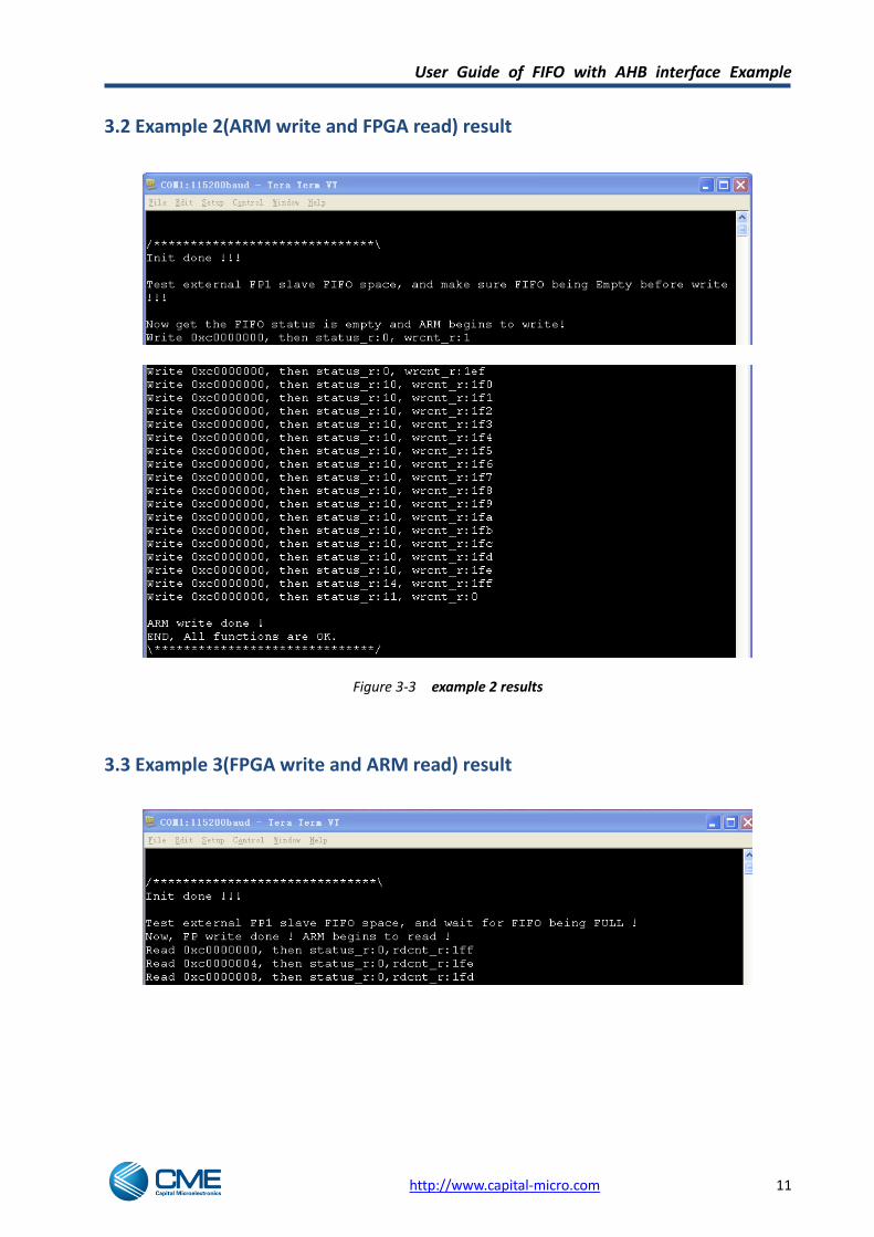
- Example 2, ARM write the FIFO, FPGA read the FIFO:
FPGA send the rempty status to ARM through GPIO, so ARM makes sure the FIFO being empty,
then writes data into the FIFO through AHB FPGA slave port 1, with checking the fifo status
(prog_full/almost_full/wfull) & data-number of FIFO after each writing, till the FIFO gets full.
FPGA monitors whether the FIFO is full, after getting full it will read data from FIFO, with
verifying the read-data of each reading, and gives an verified pass & fail signal to led.
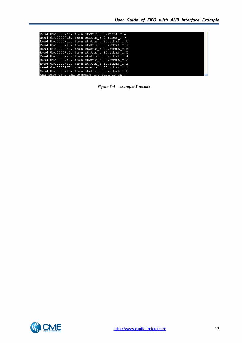
- Example 3, FPGA write the FIFO, ARM read the FIFO:
FPGA writes data into the FIFO, until the FIFO gets full.
FPGA sends the wfull status to ARM through GPIO and ARM monitors whether the FIFO is full,
after getting full it will read data from the FIFO through AHB FPGA slave port 1, with checking
status (prog_empty/almost_empty/rempty) & data-number of FIFO and verifying the data read
from FIFO after each reading, till the FIFO gets empty.
The example works at
- FPGA Array logic: 50MHz
- ARM core: 200MHz
Device: CME-M7
User Guide of FIFO with AHB interface Example
http://www.capital-micro.com 4
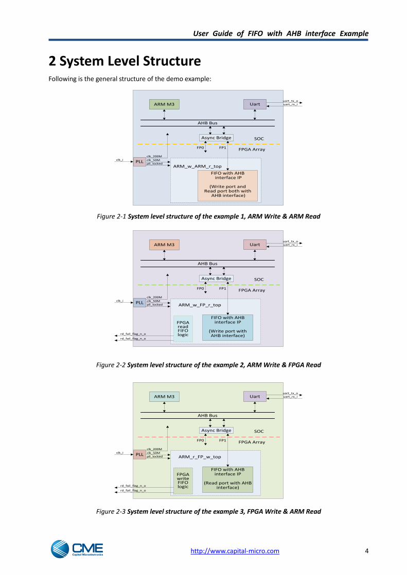
2 System Level Structure Following is the general structure of the demo example:
clk_i
uart_tx_o
ARM M3 uart_rx_i
AHB Bus
Uart
SOC
FPGA Array
PLL
clk_200Mclk_50Mpll_locked
Async Bridge
FIFO with AHB interface IP
(Write port andRead port both with
AHB interface)
FP1FP0
ARM_w_ARM_r_top
Figure 2-1 System level structure of the example 1, ARM Write & ARM Read
clk_i
uart_tx_o
ARM M3 uart_rx_i
AHB Bus
Uart
SOC
FPGA Array
PLL
clk_200Mclk_50Mpll_locked
Async Bridge
FIFO with AHB interface IP
(Write port with AHB interface)
FP1FP0
FPGA read FIFO logicrd_fail_flag_n_o
rd_fail_flag_n_o
ARM_w_FP_r_top
Figure 2-2 System level structure of the example 2, ARM Write & FPGA Read
clk_i
uart_tx_o
ARM M3 uart_rx_i
AHB Bus
Uart
SOC
FPGA Array
PLL
clk_200Mclk_50Mpll_locked
Async Bridge
FIFO with AHB interface IP
(Read port with AHB interface)
FP1FP0
FPGA write FIFO logicrd_fail_flag_n_o
rd_fail_flag_n_o
ARM_r_FP_w_top
Figure 2-3 System level structure of the example 3, FPGA Write & ARM Read
User Guide of FIFO with AHB interface Example
http://www.capital-micro.com 5
This above 3 examples each consists of 3 parts as shown in above figure: PLL, SOC/ARM, AHB interface FIFO.
They have similar structure, the same PLL configuration, the same ARM configuration. But they are different
from firmware in ARM and AHB interface FIFO configuration.
Also the 3 examples have similar design source files, which can be seen in detail in Part 4.3 Design Source.
Following is the detail of the 3 parts, PLL, SOC/ARM, FPGA-Logic-with-FIFO:
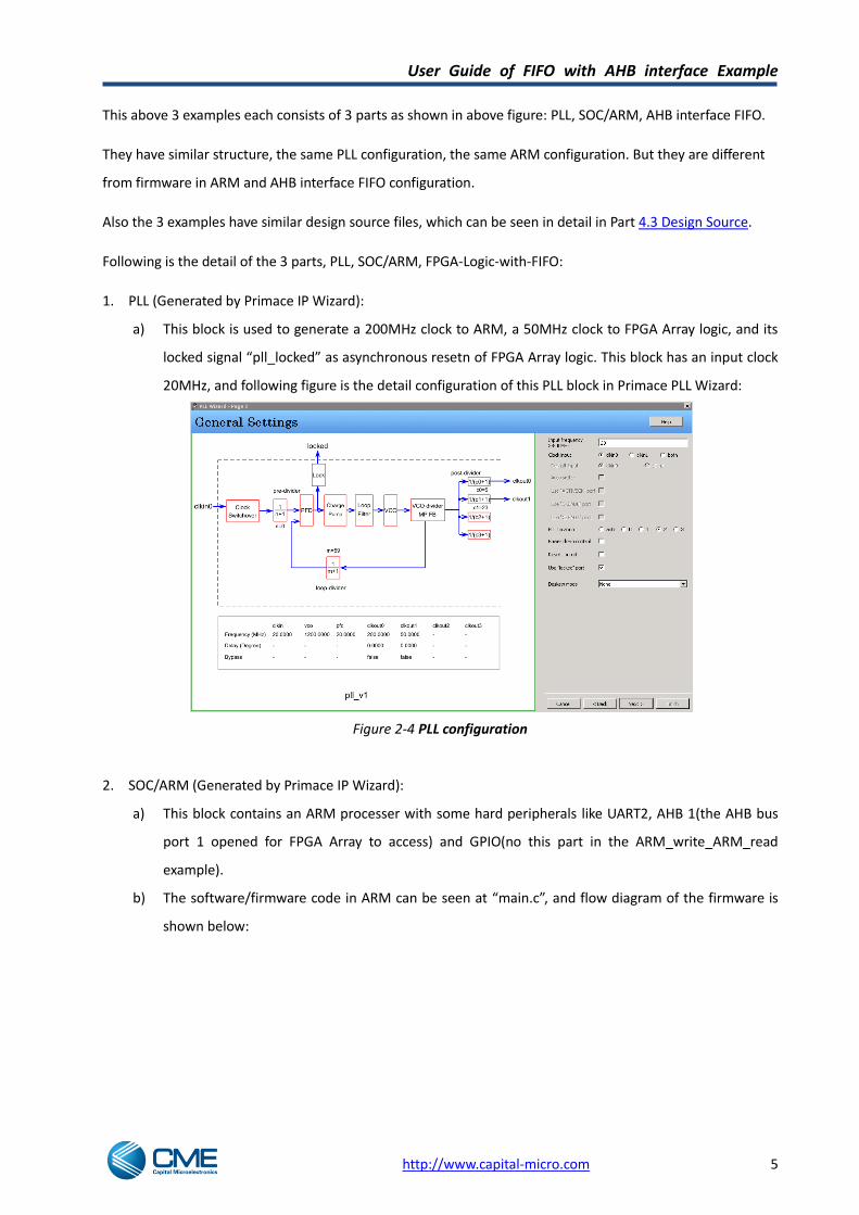
1. PLL (Generated by Primace IP Wizard):
a) This block is used to generate a 200MHz clock to ARM, a 50MHz clock to FPGA Array logic, and its
locked signal “pll_locked” as asynchronous resetn of FPGA Array logic. This block has an input clock
20MHz, and following figure is the detail configuration of this PLL block in Primace PLL Wizard:
Figure 2-4 PLL configuration
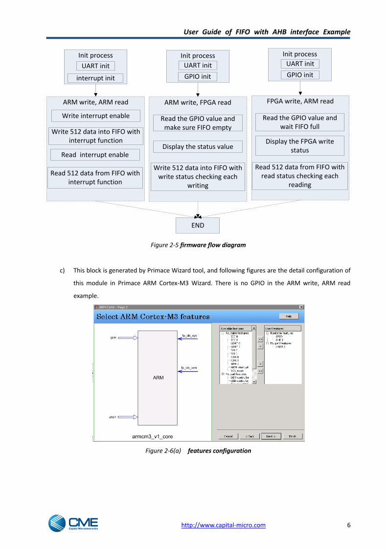
2. SOC/ARM (Generated by Primace IP Wizard):
a) This block contains an ARM processer with some hard peripherals like UART2, AHB 1(the AHB bus
port 1 opened for FPGA Array to access) and GPIO(no this part in the ARM_write_ARM_read
example).
b) The software/firmware code in ARM can be seen at “main.c”, and flow diagram of the firmware is
shown below:
User Guide of FIFO with AHB interface Example
http://www.capital-micro.com 6
Init process
UART init
ARM write, ARM read
Write 512 data into FIFO with interrupt function
Read 512 data from FIFO with interrupt function
END
Write interrupt enable
ARM write, FPGA read
Read the GPIO value and make sure FIFO empty
Write 512 data into FIFO with write status checking each
writing
Display the status value
FPGA write, ARM read
Read the GPIO value and wait FIFO full
Read 512 data from FIFO with read status checking each
reading
Display the FPGA write status
Init process
UART init
interrupt init GPIO init
Init process
UART init
GPIO init
Read interrupt enable
Figure 2-5 firmware flow diagram
c) This block is generated by Primace Wizard tool, and following figures are the detail configuration of
this module in Primace ARM Cortex-M3 Wizard. There is no GPIO in the ARM write, ARM read
example.
Figure 2-6(a) features configuration

User Guide of FIFO with AHB interface Example
http://www.capital-micro.com 7
Figure 2-6(b) set clock
Figure 2-6(c) set hex file
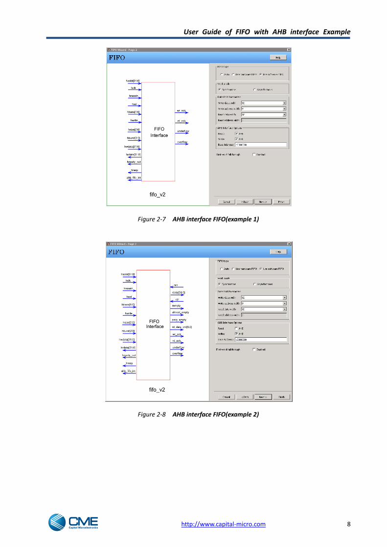
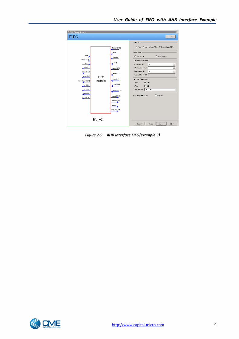
3. AHB interface FIFO (generated by Wizard)
User Guide of FIFO with AHB interface Example
http://www.capital-micro.com 8
Figure 2-7 AHB interface FIFO(example 1)
Figure 2-8 AHB interface FIFO(example 2)
User Guide of FIFO with AHB interface Example
http://www.capital-micro.com 9
Figure 2-9 AHB interface FIFO(example 3)

User Guide of FIFO with AHB interface Example
http://www.capital-micro.com 10
3 Example Result Following is the result printed to UART serial port(Use Tera-Term to fetch the serial port data):
Figure 3-1 serial port tool configuration
3.1 Example 1(ARM write and ARM read) results
Figure 3-2 example 1 results
User Guide of FIFO with AHB interface Example
http://www.capital-micro.com 11
3.2 Example 2(ARM write and FPGA read) result
Figure 3-3 example 2 results
3.3 Example 3(FPGA write and ARM read) result
User Guide of FIFO with AHB interface Example
http://www.capital-micro.com 12
Figure 3-4 example 3 results
User Guide of FIFO with AHB interface Example
http://www.capital-micro.com 13
4 Pin and Design Source description
4.1 Pin descriptions
Example 1 and 3 has the same I/O, example 2 has 2 extra Outputs contrast with example 1 and 3.
Table 4-1 The AHB-FIFO Demo top module pin description(same for 3 example)
Name Direction Width Description
clk_i Input 1 Clock input (20MHz)
rstn_i Input 1 FPGA logic reset input, low active
Table 4-2 The AHB-FIFO Demo top module pin description(the extra I/O for example 2)
Name Direction Width Description
rd_fail_flag_n_o Output 1 FP read data from FIFO verified fail signal
rd_pass_flag_n_o Output 1 FP read data from FIFO verified pass signal
4.2 Pin assignments
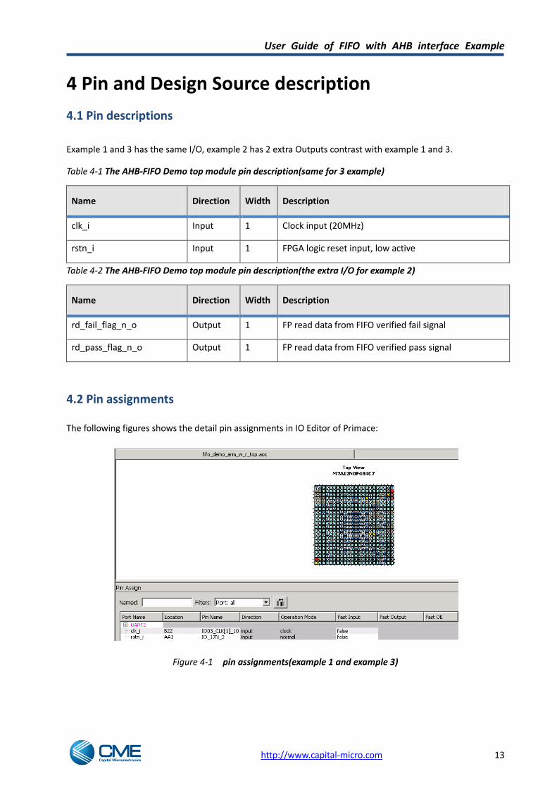
The following figures shows the detail pin assignments in IO Editor of Primace:
Figure 4-1 pin assignments(example 1 and example 3)

User Guide of FIFO with AHB interface Example
http://www.capital-micro.com 14
Figure 4-2 pin assignments(example 2)
4.3 Design Source
The AHB-FIFO Demo example RTL source files are shown in the following table 4-2, the 3 examples have the
same RTL source files except “TOP_MODULE.v”, and same firmware name “main.c” with different content.
Table 4-3 The AHB-FIFO Demo example’s source files description
File Description
RTL
./src/
example 1:fifo_demo_arm_w_arm_r.zip/fifo_demo_arm_w_arm_r/.
example 2:fifo_demo_arm_w_fp_r.zip/fifo_demo_arm_w_fp_r/.
example 3:fifo_demo_ arm_r_fp_w.zip/fifo_demo_ arm_r_fp_w /.
/TOP_MODULE.v The top module, containing FPGA-write/read-FIFO-logic, instantiates
“pll_v1.v”, “armcm3_v1_core.v” and “fifo_v2.v”. And TOP_MODULE
means:
example 1: fifo_demo_arm_w_r_top
example 2: fifo_arm_w_fp_r_top
example 3: fifo_fp_w_arm_r_top
/pll_v1.v Phase-locked loop, implemented by PLL Wizard
/armcm3_v1_core.v The ARM processor core implemented by ARM Wizard
/ fifo_v2. v This module is FIFO with AHB interface which generated by Wizard.
User Guide of FIFO with AHB interface Example
http://www.capital-micro.com 15
Three examples have different configuration.
Firmware
/main.c UART, Interrupt and GPIO initiate, and FPGA-slave-FIFO accessed by ARM
User Guide of FIFO with AHB interface Example
http://www.capital-micro.com 16
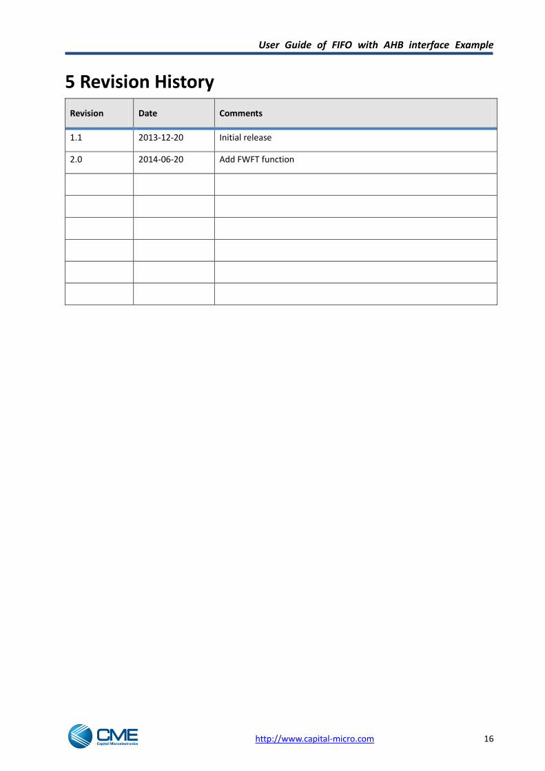
5 Revision History
Revision Date Comments
1.1 2013-12-20 Initial release
2.0 2014-06-20 Add FWFT function
Related Documents