Polymer surface texturing for direct inkjet patterning by atmospheric pressure plasma treatment† Jae Beom Park, a Jae Yong Choi, b Suk Han Lee, b Yong Seol Song c and Geun Young Yeom * a Received 5th December 2011, Accepted 20th February 2012 DOI: 10.1039/c2sm07305f It would be beneficial if the substrate surface were treated to have hydrophobic properties, in order to keep the line pattern fine during the inkjet processing, while at the same time having improved adhesion properties on the substrate. In this study, a polyimide surface was textured using atmospheric pressure plasma treatment for fine line metal inkjet printing by micromasking the surface followed by etching the polyimide surface selectively. The water contact angle on the textured polyimide film was measured to be over 100 degrees, showing that the surface was hydrophobic. When the textured polyimide surface was printed on using an electro-hydro-dynamic inkjet for Ag line printing, not only fine line Ag printing, but also improved adhesion of Ag to the polyimide surface could be obtained while maintaining excellent resistivity. The improved adhesion properties in addition to the fine line patterning afforded by texturing the polyimide surface were caused by the increased surface contact area between the metal ink and the polyimide surface during the annealing of the Ag line. 1. Introduction The manufacturing process of the microelectronic industry generally uses the photolithographic method, which consists of complicated process steps such as photomask fabrication, thin film deposition, spin-coating of a photoresist, ultraviolet (UV) light exposure, developing, and etching. These complicated, expensive, and time-consuming processes incur high manufacturing costs due to the expensive equipment required and the waste of expensive materials. 1–3 The application of a direct writing process such as ink-jet printing technology to microelectronic processing has various advantages, such as low cost, no waste of material, easier variation of the pattern shape, etc., compared to the conventional lithographic method. There- fore, the ink-jet printing process is considered to be one of the next generation microelectronic processing technologies that can be applied to flat panel displays. In addition, the ink-jet printing process is potentially a low-temperature process that may enable manufacturing on flexible substrates. Also, it is compatible with continuous roll-to-roll processing and scales more favorably with increasing substrate area than the lithographic process. 4–8 However, controlling the pattern size is a highly critical issue for the application of ink-jet printing to industrial manufacturing processes, especially for metal inkjet processing such as Ag, Cu, etc. Generally, the substrate heating method is used to obtain fine patterns during the inkjet process for the purpose of preventing the ink from spreading after printing on the substrate. But this method induces side effects such as the nozzle clogging effect, etc. 9–11 For example, H. Meier et al. 12 successfully printed 25 mm- width silver lines on a flat polyimide surface by controlling the droplet size. However, a heated substrate of 55 C had to be used to obtain fine line patterns and, even though they did not mention it, a nozzle clogging effect will exist in addition to the adhesion problem. The control of the pattern size of the printed liquid depends on the surface-wetting properties; in other words, when water droplets are dropped onto a surface, the width and configuration of the droplet pattern are mainly determined by their surface-wetting properties. Typically, a hydrophilic surface has a small contact angle and is favorable to obtain good adhesion between the metal pattern and the surface of the substrate, but this hydrophilic surface is unfavorable in keeping the pattern width fine due to the spreading of the liquid. On the other hand, a substrate having hydrophobic surface charac- teristics has a large contact angle and tends to keep the pattern width of the inkjet extruding from the nozzle narrow. However, the printed inkjet pattern generally has poor adhesion to the substrate surface. 6,8,13 That is, both surface wetting properties, hydrophilic and hydrophobic, have unfavorable characteristics for metal fine line patterning using the inkjet printing process. It would be beneficial if the substrate surface were treated so as to have hydrophobic properties, in order to keep the line pattern fine during the inkjet processing, while at the same time having a SKKU Advanced Institute of Nano Technology (SAINT), Sungkyunkwan University, Suwon, Kyunggi-do, South Korea 440-746. E-mail: gyyeom@ skku.edu; Fax: +82-31-299-6565; Tel: +82-31-299-6560 b School of Information and Communication Engineering, Sungkyunkwan University, Suwon, Kyunggi-do, South Korea 440-746 c AMOGREENTECH 185-1 Tongjin-eup Gimpo, KyungGi-Do, South Korea 415-868 † Electronic supplementary information (ESI) available. See DOI: 10.1039/c2sm07305f 5020 | Soft Matter , 2012, 8, 5020–5026 This journal is ª The Royal Society of Chemistry 2012 Dynamic Article Links C < Soft Matter Cite this: Soft Matter , 2012, 8, 5020 www.rsc.org/softmatter PAPER Downloaded by Sungkyunkwan University on 12 June 2012 Published on 22 March 2012 on http://pubs.rsc.org | doi:10.1039/C2SM07305F View Online / Journal Homepage / Table of Contents for this issue

Welcome message from author
This document is posted to help you gain knowledge. Please leave a comment to let me know what you think about it! Share it to your friends and learn new things together.
Transcript
Dynamic Article LinksC<Soft Matter
Cite this: Soft Matter, 2012, 8, 5020
www.rsc.org/softmatter PAPER
Dow
nloa
ded
by S
ungk
yunk
wan
Uni
vers
ity o
n 12
Jun
e 20
12Pu
blis
hed
on 2
2 M
arch
201
2 on
http
://pu
bs.r
sc.o
rg |
doi:1
0.10
39/C
2SM
0730
5FView Online / Journal Homepage / Table of Contents for this issue
Polymer surface texturing for direct inkjet patterning by atmosphericpressure plasma treatment†
Jae Beom Park,a Jae Yong Choi,b Suk Han Lee,b Yong Seol Songc and Geun Young Yeom*a
Received 5th December 2011, Accepted 20th February 2012
DOI: 10.1039/c2sm07305f
It would be beneficial if the substrate surface were treated to have hydrophobic properties, in order to
keep the line pattern fine during the inkjet processing, while at the same time having improved adhesion
properties on the substrate. In this study, a polyimide surface was textured using atmospheric pressure
plasma treatment for fine line metal inkjet printing by micromasking the surface followed by etching the
polyimide surface selectively. The water contact angle on the textured polyimide film was measured to
be over 100 degrees, showing that the surface was hydrophobic. When the textured polyimide surface
was printed on using an electro-hydro-dynamic inkjet for Ag line printing, not only fine line Ag
printing, but also improved adhesion of Ag to the polyimide surface could be obtained while
maintaining excellent resistivity. The improved adhesion properties in addition to the fine line
patterning afforded by texturing the polyimide surface were caused by the increased surface contact
area between the metal ink and the polyimide surface during the annealing of the Ag line.
1. Introduction
The manufacturing process of the microelectronic industry
generally uses the photolithographic method, which consists of
complicated process steps such as photomask fabrication, thin
film deposition, spin-coating of a photoresist, ultraviolet (UV)
light exposure, developing, and etching. These complicated,
expensive, and time-consuming processes incur high
manufacturing costs due to the expensive equipment required
and the waste of expensive materials.1–3 The application of
a direct writing process such as ink-jet printing technology to
microelectronic processing has various advantages, such as low
cost, no waste of material, easier variation of the pattern shape,
etc., compared to the conventional lithographic method. There-
fore, the ink-jet printing process is considered to be one of the
next generation microelectronic processing technologies that can
be applied to flat panel displays. In addition, the ink-jet printing
process is potentially a low-temperature process that may enable
manufacturing on flexible substrates. Also, it is compatible with
continuous roll-to-roll processing and scales more favorably with
increasing substrate area than the lithographic process.4–8
aSKKUAdvanced Institute of Nano Technology (SAINT), SungkyunkwanUniversity, Suwon, Kyunggi-do, South Korea 440-746. E-mail: [email protected]; Fax: +82-31-299-6565; Tel: +82-31-299-6560bSchool of Information and Communication Engineering, SungkyunkwanUniversity, Suwon, Kyunggi-do, South Korea 440-746cAMOGREENTECH 185-1 Tongjin-eup Gimpo, KyungGi-Do, SouthKorea 415-868
† Electronic supplementary information (ESI) available. See DOI:10.1039/c2sm07305f
5020 | Soft Matter, 2012, 8, 5020–5026
However, controlling the pattern size is a highly critical issue
for the application of ink-jet printing to industrial manufacturing
processes, especially for metal inkjet processing such as Ag, Cu,
etc.Generally, the substrate heating method is used to obtain fine
patterns during the inkjet process for the purpose of preventing
the ink from spreading after printing on the substrate. But this
method induces side effects such as the nozzle clogging effect,
etc.9–11 For example, H. Meier et al.12 successfully printed 25 mm-
width silver lines on a flat polyimide surface by controlling the
droplet size. However, a heated substrate of 55 �C had to be used
to obtain fine line patterns and, even though they did not
mention it, a nozzle clogging effect will exist in addition to the
adhesion problem. The control of the pattern size of the printed
liquid depends on the surface-wetting properties; in other words,
when water droplets are dropped onto a surface, the width and
configuration of the droplet pattern are mainly determined by
their surface-wetting properties. Typically, a hydrophilic surface
has a small contact angle and is favorable to obtain good
adhesion between the metal pattern and the surface of the
substrate, but this hydrophilic surface is unfavorable in keeping
the pattern width fine due to the spreading of the liquid. On the
other hand, a substrate having hydrophobic surface charac-
teristics has a large contact angle and tends to keep the pattern
width of the inkjet extruding from the nozzle narrow. However,
the printed inkjet pattern generally has poor adhesion to the
substrate surface.6,8,13 That is, both surface wetting properties,
hydrophilic and hydrophobic, have unfavorable characteristics
for metal fine line patterning using the inkjet printing process.
It would be beneficial if the substrate surface were treated so as
to have hydrophobic properties, in order to keep the line pattern
fine during the inkjet processing, while at the same time having
This journal is ª The Royal Society of Chemistry 2012
Dow
nloa
ded
by S
ungk
yunk
wan
Uni
vers
ity o
n 12
Jun
e 20
12Pu
blis
hed
on 2
2 M
arch
201
2 on
http
://pu
bs.r
sc.o
rg |
doi:1
0.10
39/C
2SM
0730
5F
View Online
improved adhesion properties on the substrate. In this study, the
polyimide surface was treated by atmospheric plasmas to form
a microscopic texture such as a lotus surface. The formation of
a micro- or nanostructure to achieve a superhydrophobic surface
has been investigated by many other researchers using various
processes such as polymer imprinting, self-assembly, etc.14–18
However, these processes are complicated, expensive, or difficult
to scale to large area processing. By using atmospheric pressure
plasmas, the microscopic structures could be more easily formed
on large area substrates through in-line or roll-to-roll processing,
both reproducibly and efficiently.
In addition, when microtexturing similar to a lotus surface was
formed on the polyimide surface by atmospheric pressure plasma
treatment composed of micromasking processing and selective
etch processing, not only a hydrophobic surface which maintains
a fine line pattern during the inkjet processing, but also improved
adhesion properties could be obtained. The improved adhesion
properties were caused by the increased contact surface area
between the inkjet metal line pattern and the polyimide surface,
due to the microstructure of the polyimide surface.
2. Experimental
Atmospheric discharge system
The atmospheric discharge system used in this experiment is
shown in Fig. 1. The system was composed of four electrodes.
The upper electrode was itself composed of 3 electrodes (two
power electrodes and one ground electrode) to form a remote
plasma configuration. The lower electrode which is located below
the substrate was grounded for the remote plasma configuration
or connected to a separate power supply for the biased confi-
guration. All of the electrodes were covered with a 2 mm thick
Al2O3 plate. The discharge gap of the upper electrodes was 5 mm
and the discharge gap between the upper electrodes and lower
electrode was 15 mm. The upper electrode was connected to an
AC power supply with a frequency of 30 kHz and the input
power was fixed at 360 W (an electrode voltage of about 7 kV).
The lower electrode was grounded or connected to a quasi-pulse
power supply with a frequency of 60 kHz. The input power to the
lower electrode for the biased condition was varied from 200 W
Fig. 1 Schematic diagram of a double dielectric barrier discharge-type
atmospheric pressure plasma system used in the experiment.
This journal is ª The Royal Society of Chemistry 2012
to 1000 W in this study. This double atmospheric discharge
system with the configuration of a bottom discharge in addition
to a top remote-type plasma showed a higher process efficiency
compared with other conventional dielectric barrier discharge
systems, due to the larger discharge area and higher gas disso-
ciation efficiency near the substrate.
Polymer substrate
A 50 mm thick polyimide film (SKC KOLON, Gyeonnggi-do,
Korea), which has a PDMA-ODA structure, was used as the
substrate in this study.
Gas mixture for atmospheric discharge
For the deposition of a thin silicon oxide mask layer on the
polyimide film, a hexamethyldisilazane (HMDS)/He/O2 gas
mixture for the deposition of the mask layer and a He/O2 gas
mixture for its agglomeration and oxidation were used. For the
selective etching of the polyimide surface, a He/O2/Ar gas
mixture was used and, for the removal of the mask layer, an N2/
NF3 gas mixture was used.
Direct inkjet process
For the dot and line patterning of Ag ink, an electrostatic field
induced inkjet head called the electro-hydro-dynamic (EHD)
printing system, based on EHD discharging of tiny droplets, in
which drop and jet are formed by an induced electric field was
used and the details of the printing technology can be found in
ref. 19. The ink used in this study (NPS-J, HARIMA Chemical,
Inc.) was about 57 wt% suspension of silver nanoparticles, whose
sizes ranged between 8 and 15 nm, and dispersed in tetradecane.
The viscosity and surface tension of the ink were 7–11 mPa s and
26.56 mN m�1 at room temperature, respectively.
Analyzer and measurement systems
The contact angles of deionized water on the treated (that is,
textured) and untreated polyimide film surfaces were measured
using a contact angle analyzer (SEO, Phoenix 450). The surface
images of the treated and untreated polyimide surface
morphologies were investigated by using a field emission scan-
ning electron microscope (FE-SEM: HITACHI, s-4700). The
chemical information on the treated and untreated polyimide
film surface was obtained using X-ray photoelectron spectros-
copy (XPS: Thermo VG SIGMA PROBE). The adhesion test
was progressed by using the tape method. The 3M scotch tape
was used for the adhesion test, and the Ag pattern shapes before
and after the taping were compared.
3. Results and discussion
SEM image of polymer surface
The texturing process of the polyimide substrate surface was
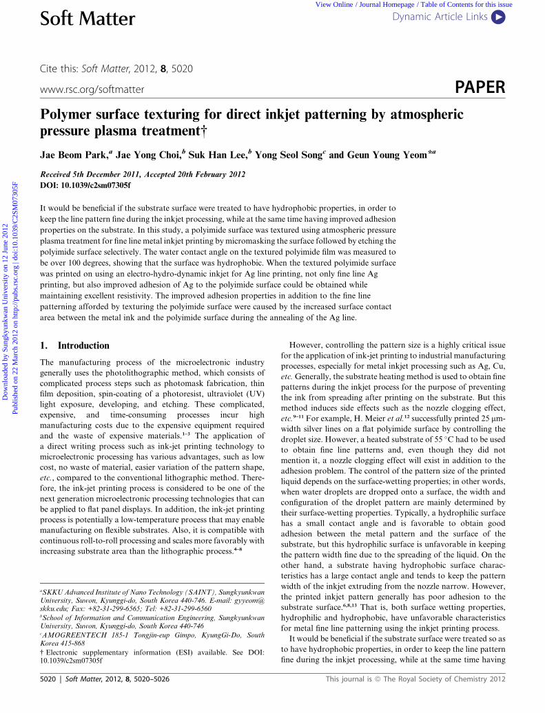
composed of four steps. Fig. 2 shows the process flow for the
polyimide microstructure texturing using atmospheric pressure
plasmas and the SEM images of the polyimide film surface after
each step: HMDS deposition (step 1), micromasking process
(step 2), selective etching of polyimide (step 3), andmask removal
Soft Matter, 2012, 8, 5020–5026 | 5021
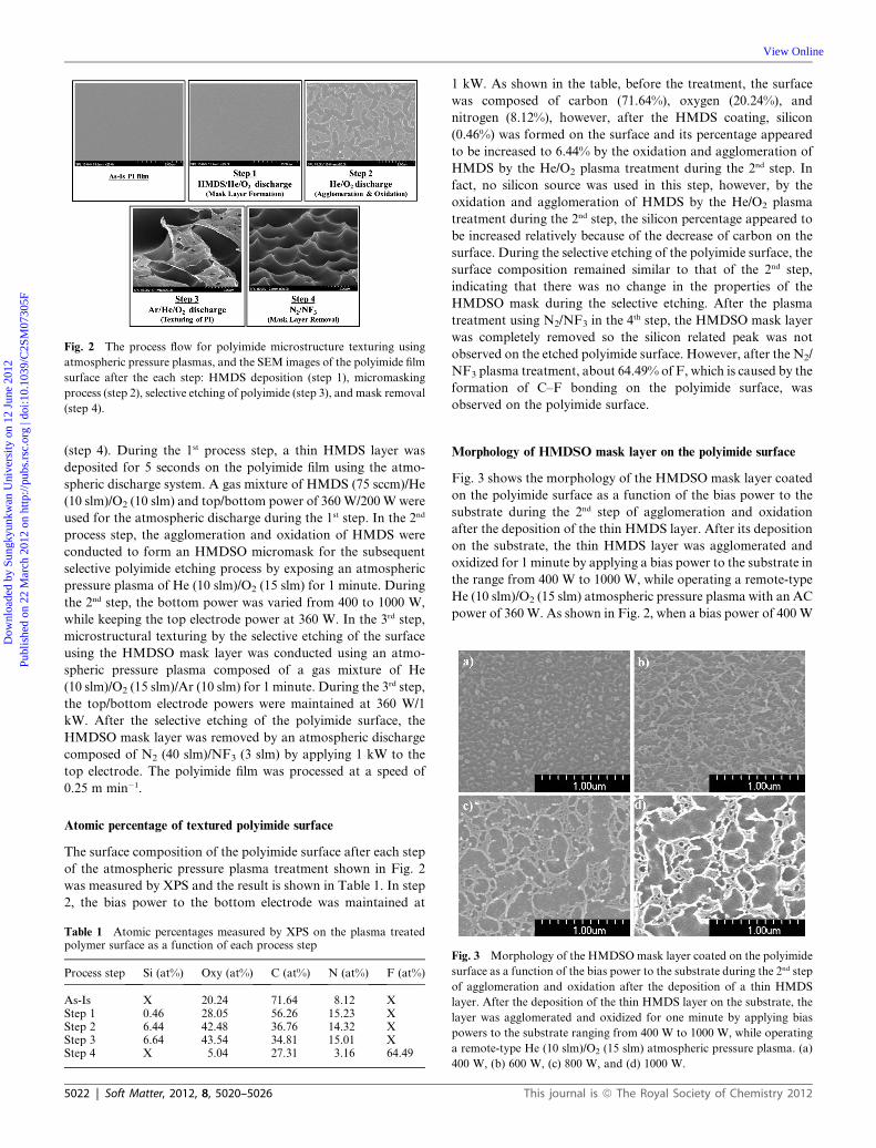
Fig. 2 The process flow for polyimide microstructure texturing using
atmospheric pressure plasmas, and the SEM images of the polyimide film
surface after the each step: HMDS deposition (step 1), micromasking
process (step 2), selective etching of polyimide (step 3), and mask removal
(step 4).
Dow
nloa
ded
by S
ungk
yunk
wan
Uni
vers
ity o
n 12
Jun
e 20
12Pu
blis
hed
on 2
2 M
arch
201
2 on
http
://pu
bs.r
sc.o
rg |
doi:1
0.10
39/C
2SM
0730
5F
View Online
(step 4). During the 1st process step, a thin HMDS layer was
deposited for 5 seconds on the polyimide film using the atmo-
spheric discharge system. A gas mixture of HMDS (75 sccm)/He
(10 slm)/O2 (10 slm) and top/bottom power of 360W/200Wwere
used for the atmospheric discharge during the 1st step. In the 2nd
process step, the agglomeration and oxidation of HMDS were
conducted to form an HMDSO micromask for the subsequent
selective polyimide etching process by exposing an atmospheric
pressure plasma of He (10 slm)/O2 (15 slm) for 1 minute. During
the 2nd step, the bottom power was varied from 400 to 1000 W,
while keeping the top electrode power at 360 W. In the 3rd step,
microstructural texturing by the selective etching of the surface
using the HMDSO mask layer was conducted using an atmo-
spheric pressure plasma composed of a gas mixture of He
(10 slm)/O2 (15 slm)/Ar (10 slm) for 1 minute. During the 3rd step,
the top/bottom electrode powers were maintained at 360 W/1
kW. After the selective etching of the polyimide surface, the
HMDSO mask layer was removed by an atmospheric discharge
composed of N2 (40 slm)/NF3 (3 slm) by applying 1 kW to the
top electrode. The polyimide film was processed at a speed of
0.25 m min�1.
Atomic percentage of textured polyimide surface
The surface composition of the polyimide surface after each step
of the atmospheric pressure plasma treatment shown in Fig. 2
was measured by XPS and the result is shown in Table 1. In step
2, the bias power to the bottom electrode was maintained at
Table 1 Atomic percentages measured by XPS on the plasma treatedpolymer surface as a function of each process step
Process step Si (at%) Oxy (at%) C (at%) N (at%) F (at%)
As-Is X 20.24 71.64 8.12 XStep 1 0.46 28.05 56.26 15.23 XStep 2 6.44 42.48 36.76 14.32 XStep 3 6.64 43.54 34.81 15.01 XStep 4 X 5.04 27.31 3.16 64.49
5022 | Soft Matter, 2012, 8, 5020–5026
1 kW. As shown in the table, before the treatment, the surface
was composed of carbon (71.64%), oxygen (20.24%), and
nitrogen (8.12%), however, after the HMDS coating, silicon
(0.46%) was formed on the surface and its percentage appeared
to be increased to 6.44% by the oxidation and agglomeration of
HMDS by the He/O2 plasma treatment during the 2nd step. In
fact, no silicon source was used in this step, however, by the
oxidation and agglomeration of HMDS by the He/O2 plasma
treatment during the 2nd step, the silicon percentage appeared to
be increased relatively because of the decrease of carbon on the
surface. During the selective etching of the polyimide surface, the
surface composition remained similar to that of the 2nd step,
indicating that there was no change in the properties of the
HMDSO mask during the selective etching. After the plasma
treatment using N2/NF3 in the 4th step, the HMDSO mask layer
was completely removed so the silicon related peak was not
observed on the etched polyimide surface. However, after the N2/
NF3 plasma treatment, about 64.49% of F, which is caused by the
formation of C–F bonding on the polyimide surface, was
observed on the polyimide surface.
Morphology of HMDSO mask layer on the polyimide surface
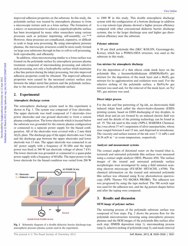
Fig. 3 shows the morphology of the HMDSO mask layer coated
on the polyimide surface as a function of the bias power to the
substrate during the 2nd step of agglomeration and oxidation
after the deposition of the thin HMDS layer. After its deposition
on the substrate, the thin HMDS layer was agglomerated and
oxidized for 1 minute by applying a bias power to the substrate in
the range from 400 W to 1000 W, while operating a remote-type
He (10 slm)/O2 (15 slm) atmospheric pressure plasma with an AC
power of 360W. As shown in Fig. 2, when a bias power of 400 W
Fig. 3 Morphology of the HMDSOmask layer coated on the polyimide
surface as a function of the bias power to the substrate during the 2nd step
of agglomeration and oxidation after the deposition of a thin HMDS
layer. After the deposition of the thin HMDS layer on the substrate, the
layer was agglomerated and oxidized for one minute by applying bias
powers to the substrate ranging from 400 W to 1000 W, while operating
a remote-type He (10 slm)/O2 (15 slm) atmospheric pressure plasma. (a)
400 W, (b) 600 W, (c) 800 W, and (d) 1000 W.
This journal is ª The Royal Society of Chemistry 2012
Dow
nloa
ded
by S
ungk
yunk
wan
Uni
vers
ity o
n 12
Jun
e 20
12Pu
blis
hed
on 2
2 M
arch
201
2 on
http
://pu
bs.r
sc.o
rg |
doi:1
0.10
39/C
2SM
0730
5F
View Online
was applied, only part of the surface area of the deposited thin
HMDS layer was agglomerated, showing 100–200 nm diameter
particle-type HMDSO on the polyimide surface. By increasing
the bias power to 600 W, a fiber (or ribbon)-type network of
HMDSO with a size of a few hundred nanometres could be
observed due to its agglomeration. When increasing the bias
power to 1000 W, the HMDSO was further agglomerated into
a thin fiber (or ribbon)-type network and the exposed polyimide
surface area was increased. It is believed that the agglomeration
of HMDSO is related to the increased stress in the film during the
oxidation and C–H removal of the deposited HMDS thin film
and the increased mobility of the surface atoms caused by the
increased ion bombardment (or heating) at the increased bias
power.20,21
Oxidation of HMDSO mask layer
Fig. 4 shows the chemical bonding state of the Si 2p in the
HMDSO formed on the polyimide surface during the 2nd step
measured as a function of the bias power (400–1000 W), while
operating a remote-type He (10 slm)/O2 (15 slm) atmospheric
pressure plasma with an AC power of 360 W. As shown in the
figure, with increasing bias power, the binding energy and
intensity of the Si 2p peak were also increased. The Si 2p peak
position was 102.21 eV for 400 W and 102.91 eV for 600 W,
which are lower than the value of 103.3 eV for Si–O2 bonding and
higher than the value of 102.1 eV for (CH3)2–Si–O2 bonding.22,23
Therefore, the HMDS layer formed on the polyimide surface was
not sufficiently oxidized by the He/O2 plasma during the 2nd step
when the bias power was less than or equal to 600W. In addition,
due to the low oxidation and agglomeration of HMDS, the peak
intensity of Si 2p was low. However, the Si 2p peak was increased
to 103.26 eV at a bias power of 800 W and 104.07 eV at 1000 W,
which is close to the silicon bonding to Si–O2 bonding at 103.3 eV
and Si–(O or OH)4 bonding at 104.3 eV, in addition to the
increase of the Si 2p peak intensity due to the further agglo-
meration on the polyimide surface.
Contact angle of textured polyimide surface
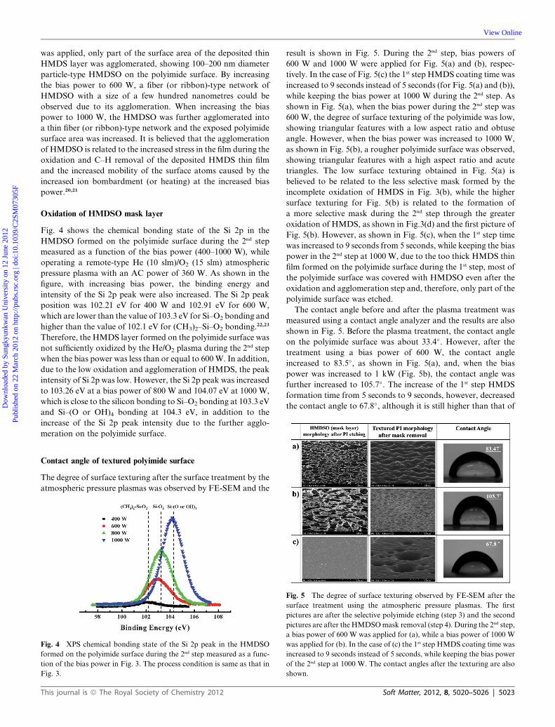
The degree of surface texturing after the surface treatment by the
atmospheric pressure plasmas was observed by FE-SEM and the
Fig. 4 XPS chemical bonding state of the Si 2p peak in the HMDSO
formed on the polyimide surface during the 2nd step measured as a func-
tion of the bias power in Fig. 3. The process condition is same as that in
Fig. 3.
This journal is ª The Royal Society of Chemistry 2012
result is shown in Fig. 5. During the 2nd step, bias powers of
600 W and 1000 W were applied for Fig. 5(a) and (b), respec-
tively. In the case of Fig. 5(c) the 1st step HMDS coating time was
increased to 9 seconds instead of 5 seconds (for Fig. 5(a) and (b)),
while keeping the bias power at 1000 W during the 2nd step. As
shown in Fig. 5(a), when the bias power during the 2nd step was
600 W, the degree of surface texturing of the polyimide was low,
showing triangular features with a low aspect ratio and obtuse
angle. However, when the bias power was increased to 1000 W,
as shown in Fig. 5(b), a rougher polyimide surface was observed,
showing triangular features with a high aspect ratio and acute
triangles. The low surface texturing obtained in Fig. 5(a) is
believed to be related to the less selective mask formed by the
incomplete oxidation of HMDS in Fig. 3(b), while the higher
surface texturing for Fig. 5(b) is related to the formation of
a more selective mask during the 2nd step through the greater
oxidation of HMDS, as shown in Fig.3(d) and the first picture of
Fig. 5(b). However, as shown in Fig. 5(c), when the 1st step time
was increased to 9 seconds from 5 seconds, while keeping the bias
power in the 2nd step at 1000 W, due to the too thick HMDS thin
film formed on the polyimide surface during the 1st step, most of
the polyimide surface was covered with HMDSO even after the
oxidation and agglomeration step and, therefore, only part of the
polyimide surface was etched.
The contact angle before and after the plasma treatment was
measured using a contact angle analyzer and the results are also
shown in Fig. 5. Before the plasma treatment, the contact angle
on the polyimide surface was about 33.4�. However, after the
treatment using a bias power of 600 W, the contact angle
increased to 83.5�, as shown in Fig. 5(a), and, when the bias
power was increased to 1 kW (Fig. 5b), the contact angle was
further increased to 105.7�. The increase of the 1st step HMDS
formation time from 5 seconds to 9 seconds, however, decreased
the contact angle to 67.8�, although it is still higher than that of
Fig. 5 The degree of surface texturing observed by FE-SEM after the
surface treatment using the atmospheric pressure plasmas. The first
pictures are after the selective polyimide etching (step 3) and the second
pictures are after the HMDSOmask removal (step 4). During the 2nd step,
a bias power of 600 W was applied for (a), while a bias power of 1000 W
was applied for (b). In the case of (c) the 1st step HMDS coating time was
increased to 9 seconds instead of 5 seconds, while keeping the bias power
of the 2nd step at 1000 W. The contact angles after the texturing are also
shown.
Soft Matter, 2012, 8, 5020–5026 | 5023
Dow
nloa
ded
by S
ungk
yunk
wan
Uni
vers
ity o
n 12
Jun
e 20
12Pu
blis
hed
on 2
2 M
arch
201
2 on
http
://pu
bs.r
sc.o
rg |
doi:1
0.10
39/C
2SM
0730
5F
View Online
the untreated polyimide surface. (When the contact angle was
measured with the tetradecane solution which is the inkjet
solution instead of DI water, complete spreading having a near
0� contact angle was observed for the untreated polyimide
surface. When the polyimide was treated with the NF3/N2
atmospheric remote plasma treatment (4th process step), the
contact angle was increased to 36.7� and, in the case of the
plasma textured polyimide, the contact angle was further
increased to 77.6�(Fig. A-3†). Therefore, by using the tetrade-
cane solution, even though the contact angle similar to that of DI
water could not be obtained, the highest contact angle could be
obtained on the plasma textured polyimide.)
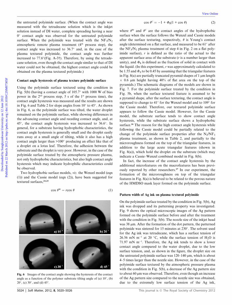
Contact angle hysteresis of plasma texture polyimide surface
Using the polyimide surface textured using the condition in
Fig. 5(b) (having a contact angle of 105.7� with 1000 W of bias
power in the 2nd process step, 5 s of the 1st process time), the
contact angle hysteresis was measured and the results are shown
in Fig. 6 and Table 2 for slope angles from 10� to 45�. As shown
in Fig. 6, as the polyimide surface was tilted, the water droplet
remained on the polyimide surface, while showing differences in
the advancing contact angle and receding contact angle, and, at
45�, the contact angle hysteresis was increased to 36.6�. In
general, for a substrate having hydrophobic characteristics, the
contact angle hysteresis is generally small and the droplet easily
runs away at a small angle of tilting, while it also has a high
contact angle larger than >100� producing an effect like that of
a droplet on a lotus leaf. Therefore, the adhesion between the
substrate and the droplet is very poor. However, in the case of the
polyimide surface treated by the atmospheric pressure plasma,
not only hydrophobic characteristics, but also high contact angle
hysteresis which may indicate hydrophilic characteristics could
be observed.
Two hydrophobic surface models, viz. the Wenzel model (eqn
(1)) and the Cassie model (eqn (2)), have been suggested for
textured surfaces,24,25
cos qW ¼ rcos q (1)
Fig. 6 Images of the contact angle showing the hysteresis of the contact
angle as a function of the polymer substrate tilting angle of (a) 10�, (b)20�, (c) 30�, and (d) 45�.
5024 | Soft Matter, 2012, 8, 5020–5026
cos qC ¼ �1 + FS(1 + cos q) (2)
where qW and qC are the contact angles of the hydrophobic
surface when the surface follows the Wenzel and Cassie models
after the surface texturing, respectively, q is Young’s contact
angle (determined on a flat surface, and measured to be 61� afterthe NF3/N2 plasma treatment of step 4 in Fig. 2 on a flat poly-
imide surface), r is defined as the ratio of the actual to the
apparent surface area of the substrate (r is a number larger than
unity), and FS is defined as the fraction of solid in contact with
the liquid. (In this experiment, r was approximately calculated to
be 1.55 andFS to be 0.45 by assuming that the triangular features
in Fig. 8(a) are partially truncated pyramid shapes of 1 mm length
� 0.6 mm height having 40% of flat area on the top of the
pyramids.) The schematic diagrams of the models are shown in
Fig. 7. For the polyimide surface treated by the condition in
Fig. 5b, when the surface textured feature is assumed to be
a pyramid shape, after the surface texturing, the contact angle is
supposed to change to 41� for the Wenzel model and to 109� forthe Cassie model. Therefore, our textured polyimide surface
appears to follow the Cassie model. However, for the Cassie
model, the substrate surface tends to show contact angle
hysteresis, while the substrate surface shows a hydrophobic
surface.26 The reason for the high contact angle hysteresis while
following the Cassie model could be partially related to the
change of the polyimide surface properties after the N2/NF3
plasma treatment, as shown in Table 2, and partially to the
microroughness formed on the top of the triangular features, in
addition to the large acute triangular features (shown in
Fig. 8(a)), which hold the droplet on the substrate (which may
indicate a Cassie–Wenzel combined model in Fig. 8(b).
In fact, the increase of the contact angle hysteresis by the
additional microfeatures on the macrofeatures has been previ-
ously reported by other researchers.27 In our experiment, the
formation of the microroughness on top of the triangular
features in Fig. 8(a) is believed to be related to the porous nature
of the HMDSO mask layer formed on the polyimide surface.
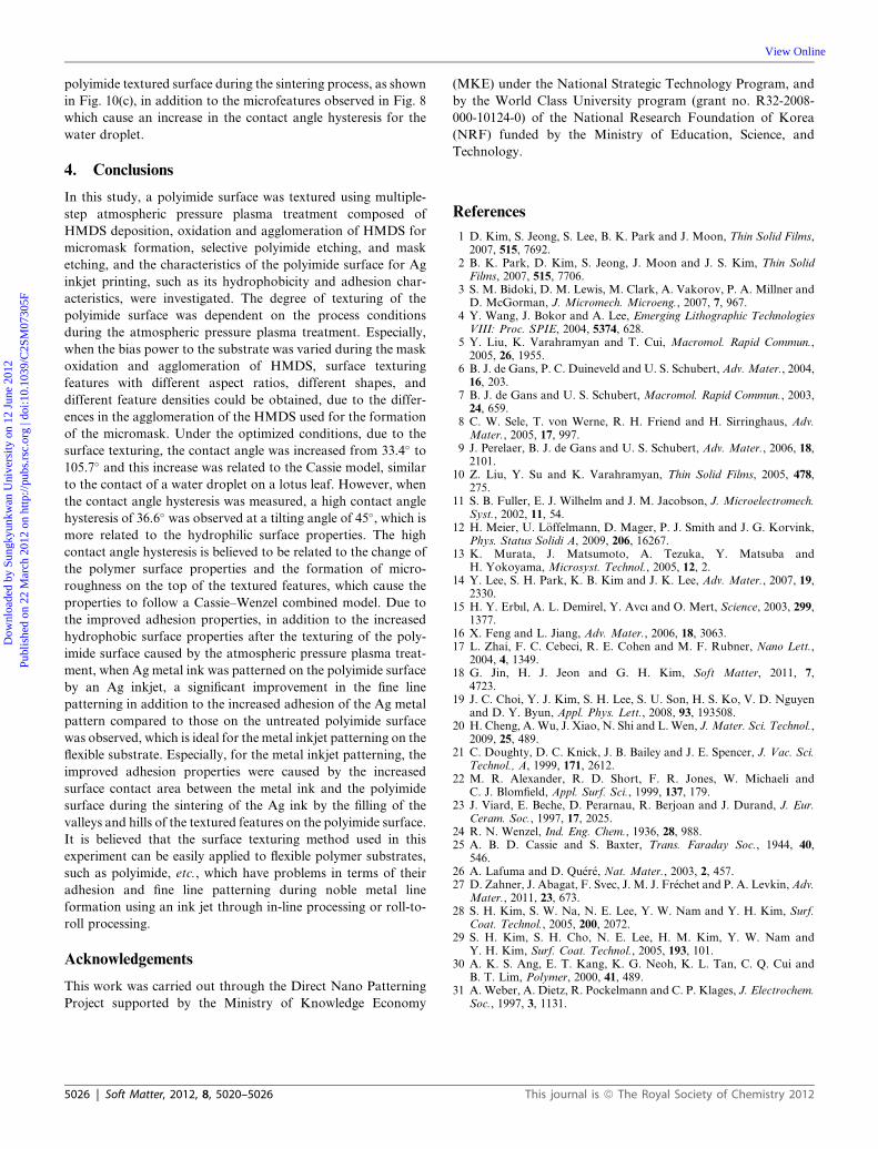
Pattern width of Ag ink on plasma textured polyimide
On the polyimide surface treated by the condition in Fig. 5(b), Ag
ink was dropped and its patterning property was investigated.
Fig. 9 shows the optical microscopic images of the Ag pattern
formed on the polyimide surface before and after the treatment
with the condition in Fig. 5(b). The nozzle size of the inkjet head
was 38 mm. After the formation of the dot pattern, the patterned
polyimide was sintered for 15 minutes at 230�. The solvent usedfor the Ag ink was tetradecane, which has a surface tension of
26.56 mN m�1 at 20 �C, while the surface tension of H2O is
71.97 mN m�1. Therefore, the Ag ink tends to show a lower
contact angle compared to the water droplet, due to the low
surface tension, and, as shown in the figure, the droplet size on
the untreated polyimide surface was 120–140 mm, which is about
4–5 times larger than the nozzle size. However, in the case of the
polyimide surface textured by the atmospheric pressure plasma
with the condition in Fig. 5(b), a decrease of the Ag pattern size
to about 60 mmwas observed. Therefore, even though an increase
of the Ag pattern size compared to the nozzle size was obtained,
due to the extremely low surface tension of the Ag ink,
This journal is ª The Royal Society of Chemistry 2012
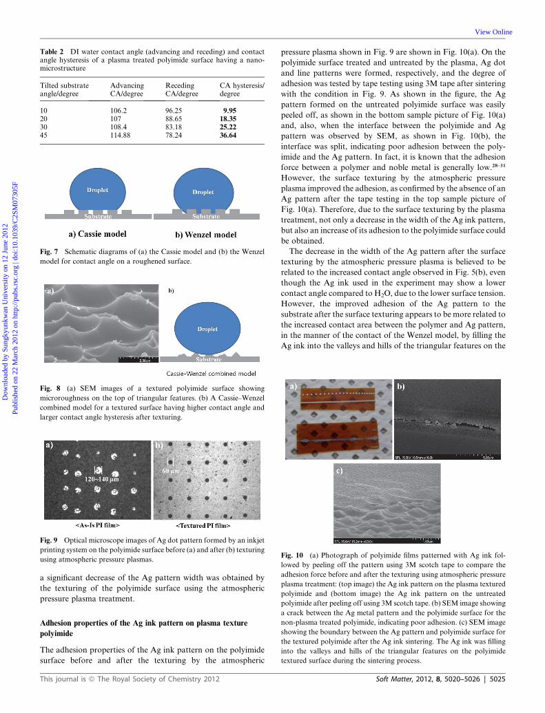
Table 2 DI water contact angle (advancing and receding) and contactangle hysteresis of a plasma treated polyimide surface having a nano-microstructure
Tilted substrateangle/degree
AdvancingCA/degree
RecedingCA/degree
CA hysteresis/degree
10 106.2 96.25 9.9520 107 88.65 18.3530 108.4 83.18 25.2245 114.88 78.24 36.64
Fig. 8 (a) SEM images of a textured polyimide surface showing
microroughness on the top of triangular features. (b) A Cassie–Wenzel
combined model for a textured surface having higher contact angle and
larger contact angle hysteresis after texturing.
Fig. 7 Schematic diagrams of (a) the Cassie model and (b) the Wenzel
model for contact angle on a roughened surface.
Fig. 9 Optical microscope images of Ag dot pattern formed by an inkjet
printing system on the polyimide surface before (a) and after (b) texturing
using atmospheric pressure plasmas.Fig. 10 (a) Photograph of polyimide films patterned with Ag ink fol-
lowed by peeling off the pattern using 3M scotch tape to compare the
adhesion force before and after the texturing using atmospheric pressure
plasma treatment: (top image) the Ag ink pattern on the plasma textured
polyimide and (bottom image) the Ag ink pattern on the untreated
polyimide after peeling off using 3M scotch tape. (b) SEM image showing
Dow
nloa
ded
by S
ungk
yunk
wan
Uni
vers
ity o
n 12
Jun
e 20
12Pu
blis
hed
on 2
2 M
arch
201
2 on
http
://pu
bs.r
sc.o
rg |
doi:1
0.10
39/C
2SM
0730
5F
View Online
a significant decrease of the Ag pattern width was obtained by
the texturing of the polyimide surface using the atmospheric
pressure plasma treatment.
a crack between the Ag metal pattern and the polyimide surface for the
non-plasma treated polyimide, indicating poor adhesion. (c) SEM image
showing the boundary between the Ag pattern and polyimide surface for
the textured polyimide after the Ag ink sintering. The Ag ink was filling
into the valleys and hills of the triangular features on the polyimide
textured surface during the sintering process.
Adhesion properties of the Ag ink pattern on plasma texture
polyimide
The adhesion properties of the Ag ink pattern on the polyimide
surface before and after the texturing by the atmospheric
This journal is ª The Royal Society of Chemistry 2012
pressure plasma shown in Fig. 9 are shown in Fig. 10(a). On the
polyimide surface treated and untreated by the plasma, Ag dot
and line patterns were formed, respectively, and the degree of
adhesion was tested by tape testing using 3M tape after sintering
with the condition in Fig. 9. As shown in the figure, the Ag
pattern formed on the untreated polyimide surface was easily
peeled off, as shown in the bottom sample picture of Fig. 10(a)
and, also, when the interface between the polyimide and Ag
pattern was observed by SEM, as shown in Fig. 10(b), the
interface was split, indicating poor adhesion between the poly-
imide and the Ag pattern. In fact, it is known that the adhesion
force between a polymer and noble metal is generally low.28–31
However, the surface texturing by the atmospheric pressure
plasma improved the adhesion, as confirmed by the absence of an
Ag pattern after the tape testing in the top sample picture of
Fig. 10(a). Therefore, due to the surface texturing by the plasma
treatment, not only a decrease in the width of the Ag ink pattern,
but also an increase of its adhesion to the polyimide surface could
be obtained.
The decrease in the width of the Ag pattern after the surface
texturing by the atmospheric pressure plasma is believed to be
related to the increased contact angle observed in Fig. 5(b), even
though the Ag ink used in the experiment may show a lower
contact angle compared to H2O, due to the lower surface tension.
However, the improved adhesion of the Ag pattern to the
substrate after the surface texturing appears to be more related to
the increased contact area between the polymer and Ag pattern,
in the manner of the contact of the Wenzel model, by filling the
Ag ink into the valleys and hills of the triangular features on the
Soft Matter, 2012, 8, 5020–5026 | 5025
Dow
nloa
ded
by S
ungk
yunk
wan
Uni
vers
ity o
n 12
Jun
e 20
12Pu
blis
hed
on 2
2 M
arch
201
2 on
http
://pu
bs.r
sc.o
rg |
doi:1
0.10
39/C
2SM
0730
5F
View Online
polyimide textured surface during the sintering process, as shown
in Fig. 10(c), in addition to the microfeatures observed in Fig. 8
which cause an increase in the contact angle hysteresis for the
water droplet.
4. Conclusions
In this study, a polyimide surface was textured using multiple-
step atmospheric pressure plasma treatment composed of
HMDS deposition, oxidation and agglomeration of HMDS for
micromask formation, selective polyimide etching, and mask
etching, and the characteristics of the polyimide surface for Ag
inkjet printing, such as its hydrophobicity and adhesion char-
acteristics, were investigated. The degree of texturing of the
polyimide surface was dependent on the process conditions
during the atmospheric pressure plasma treatment. Especially,
when the bias power to the substrate was varied during the mask
oxidation and agglomeration of HMDS, surface texturing
features with different aspect ratios, different shapes, and
different feature densities could be obtained, due to the differ-
ences in the agglomeration of the HMDS used for the formation
of the micromask. Under the optimized conditions, due to the
surface texturing, the contact angle was increased from 33.4� to105.7� and this increase was related to the Cassie model, similar
to the contact of a water droplet on a lotus leaf. However, when
the contact angle hysteresis was measured, a high contact angle
hysteresis of 36.6� was observed at a tilting angle of 45�, which is
more related to the hydrophilic surface properties. The high
contact angle hysteresis is believed to be related to the change of
the polymer surface properties and the formation of micro-
roughness on the top of the textured features, which cause the
properties to follow a Cassie–Wenzel combined model. Due to
the improved adhesion properties, in addition to the increased
hydrophobic surface properties after the texturing of the poly-
imide surface caused by the atmospheric pressure plasma treat-
ment, when Ag metal ink was patterned on the polyimide surface
by an Ag inkjet, a significant improvement in the fine line
patterning in addition to the increased adhesion of the Ag metal
pattern compared to those on the untreated polyimide surface
was observed, which is ideal for the metal inkjet patterning on the
flexible substrate. Especially, for the metal inkjet patterning, the
improved adhesion properties were caused by the increased
surface contact area between the metal ink and the polyimide
surface during the sintering of the Ag ink by the filling of the
valleys and hills of the textured features on the polyimide surface.
It is believed that the surface texturing method used in this
experiment can be easily applied to flexible polymer substrates,
such as polyimide, etc., which have problems in terms of their
adhesion and fine line patterning during noble metal line
formation using an ink jet through in-line processing or roll-to-
roll processing.
Acknowledgements
This work was carried out through the Direct Nano Patterning
Project supported by the Ministry of Knowledge Economy
5026 | Soft Matter, 2012, 8, 5020–5026
(MKE) under the National Strategic Technology Program, and
by the World Class University program (grant no. R32-2008-
000-10124-0) of the National Research Foundation of Korea
(NRF) funded by the Ministry of Education, Science, and
Technology.
References
1 D. Kim, S. Jeong, S. Lee, B. K. Park and J. Moon, Thin Solid Films,2007, 515, 7692.
2 B. K. Park, D. Kim, S. Jeong, J. Moon and J. S. Kim, Thin SolidFilms, 2007, 515, 7706.
3 S. M. Bidoki, D. M. Lewis, M. Clark, A. Vakorov, P. A. Millner andD. McGorman, J. Micromech. Microeng., 2007, 7, 967.
4 Y. Wang, J. Bokor and A. Lee, Emerging Lithographic TechnologiesVIII: Proc. SPIE, 2004, 5374, 628.
5 Y. Liu, K. Varahramyan and T. Cui, Macromol. Rapid Commun.,2005, 26, 1955.
6 B. J. de Gans, P. C. Duineveld and U. S. Schubert, Adv. Mater., 2004,16, 203.
7 B. J. de Gans and U. S. Schubert, Macromol. Rapid Commun., 2003,24, 659.
8 C. W. Sele, T. von Werne, R. H. Friend and H. Sirringhaus, Adv.Mater., 2005, 17, 997.
9 J. Perelaer, B. J. de Gans and U. S. Schubert, Adv. Mater., 2006, 18,2101.
10 Z. Liu, Y. Su and K. Varahramyan, Thin Solid Films, 2005, 478,275.
11 S. B. Fuller, E. J. Wilhelm and J. M. Jacobson, J. Microelectromech.Syst., 2002, 11, 54.
12 H. Meier, U. L€offelmann, D. Mager, P. J. Smith and J. G. Korvink,Phys. Status Solidi A, 2009, 206, 16267.
13 K. Murata, J. Matsumoto, A. Tezuka, Y. Matsuba andH. Yokoyama, Microsyst. Technol., 2005, 12, 2.
14 Y. Lee, S. H. Park, K. B. Kim and J. K. Lee, Adv. Mater., 2007, 19,2330.
15 H. Y. Erbıl, A. L. Demirel, Y. Avcı and O. Mert, Science, 2003, 299,1377.
16 X. Feng and L. Jiang, Adv. Mater., 2006, 18, 3063.17 L. Zhai, F. C. Cebeci, R. E. Cohen and M. F. Rubner, Nano Lett.,
2004, 4, 1349.18 G. Jin, H. J. Jeon and G. H. Kim, Soft Matter, 2011, 7,
4723.19 J. C. Choi, Y. J. Kim, S. H. Lee, S. U. Son, H. S. Ko, V. D. Nguyen
and D. Y. Byun, Appl. Phys. Lett., 2008, 93, 193508.20 H. Cheng, A.Wu, J. Xiao, N. Shi and L.Wen, J. Mater. Sci. Technol.,
2009, 25, 489.21 C. Doughty, D. C. Knick, J. B. Bailey and J. E. Spencer, J. Vac. Sci.
Technol., A, 1999, 171, 2612.22 M. R. Alexander, R. D. Short, F. R. Jones, W. Michaeli and
C. J. Blomfield, Appl. Surf. Sci., 1999, 137, 179.23 J. Viard, E. Beche, D. Perarnau, R. Berjoan and J. Durand, J. Eur.
Ceram. Soc., 1997, 17, 2025.24 R. N. Wenzel, Ind. Eng. Chem., 1936, 28, 988.25 A. B. D. Cassie and S. Baxter, Trans. Faraday Soc., 1944, 40,
546.26 A. Lafuma and D. Qu�er�e, Nat. Mater., 2003, 2, 457.27 D. Zahner, J. Abagat, F. Svec, J. M. J. Fr�echet and P. A. Levkin,Adv.
Mater., 2011, 23, 673.28 S. H. Kim, S. W. Na, N. E. Lee, Y. W. Nam and Y. H. Kim, Surf.
Coat. Technol., 2005, 200, 2072.29 S. H. Kim, S. H. Cho, N. E. Lee, H. M. Kim, Y. W. Nam and
Y. H. Kim, Surf. Coat. Technol., 2005, 193, 101.30 A. K. S. Ang, E. T. Kang, K. G. Neoh, K. L. Tan, C. Q. Cui and
B. T. Lim, Polymer, 2000, 41, 489.31 A. Weber, A. Dietz, R. Pockelmann and C. P. Klages, J. Electrochem.
Soc., 1997, 3, 1131.
This journal is ª The Royal Society of Chemistry 2012
Related Documents