41 Chapter 4 Electrical Properties of Graphene Wrinkles and Nanoribbons Part of the contents presented in this chapter are based on Xu, K., Cao, P.G. and Heath, J.R. "Scanning tunneling microscopy characterization of the electrical properties of wrinkles in exfoliated graphene monolayers," Nano Lett, 9, 4446-4451 (2009). (Ref. 1 ) 4.1 Introduction Graphene refers to a monolayer of carbon atoms tightly packed into a two-dimensional (2D) honeycomb lattice. The discovery of graphene in an isolated state 2, 3 has generated widespread research interest. 4-6 The linear dispersion spectrum of graphene causes its charge carriers to behave like massless Dirac fermions, leading to various novel electrical properties that are of fundamental interest. Meanwhile, the unique structure of graphene, in which all atoms are surface atoms, makes its electronic band structure and hence electrical properties extremely sensitive to size effects, surface curvatures, as well as environmental interactions. 4.1.1 Wrinkles in graphene Graphene initially appeared to be a strictly 2D electronic system, and quantum Hall effects were observed in graphene up to room temperature. 7 On the other hand,

Welcome message from author
This document is posted to help you gain knowledge. Please leave a comment to let me know what you think about it! Share it to your friends and learn new things together.
Transcript
41
Chapter 4
Electrical Properties of Graphene Wrinkles
and Nanoribbons
Part of the contents presented in this chapter are based on Xu, K., Cao, P.G. and Heath, J.R. "Scanning
tunneling microscopy characterization of the electrical properties of wrinkles in exfoliated graphene
monolayers," Nano Lett, 9, 4446-4451 (2009). (Ref.1)
4.1 Introduction
Graphene refers to a monolayer of carbon atoms tightly packed into a two-dimensional
(2D) honeycomb lattice. The discovery of graphene in an isolated state2, 3 has generated
widespread research interest.4-6 The linear dispersion spectrum of graphene causes its
charge carriers to behave like massless Dirac fermions, leading to various novel electrical
properties that are of fundamental interest. Meanwhile, the unique structure of graphene,
in which all atoms are surface atoms, makes its electronic band structure and hence
electrical properties extremely sensitive to size effects, surface curvatures, as well as
environmental interactions.
4.1.1 Wrinkles in graphene
Graphene initially appeared to be a strictly 2D electronic system, and quantum
Hall effects were observed in graphene up to room temperature.7 On the other hand,
42
theory has predicted that strictly 2D crystals are thermodynamically unstable and
therefore should not exist at any finite temperature.8
This contradiction was reconciled by recent transmission electron microscopy
(TEM) studies on suspended graphene, in which a microscopically corrugated three-
dimensional structure was revealed,9, 10 overturning the naïve picture of graphene being a
flat 2D crystal. The <1 nm local corrugations (“ripples”) discovered in these TEM studies
are believed to be intrinsic,11 and so are important for understanding graphene electrical
properties.5, 12-16 The low resolution of TEM, especially in the vertical direction, however,
limits further detailed studies of these corrugations, and how those corrugations can
influence the graphene properties. In addition, the structure and properties of suspended
graphene may be fundamentally different from graphene deposited on SiO2 substrates,
the most widely studied form of graphene.
Scanning tunneling microscopy (STM) provides a valuable alternative, which
probes morphology and electrical properties at atomic resolution in all three dimensions.
Atomically resolved STM topographs of graphene on SiO2 substrates have been
reported,17-21 from which the height of graphene ripples was determined to be 3-5 Å.
Meanwhile, attempts to correlate local electrical properties with the observed ripples have
achieved only limited success.21-23
In this chapter, we report on the STM study of a new class of corrugations in
monolayer graphene sheets that have been largely neglected in previous studies, i.e.,
wrinkles ~10 nm in width and ~3 nm in height. We found such corrugations to be
ubiquitous in graphene, and have distinctly different properties in comparison to other
43
regions of graphene that only contain small ripples. In particular, a “three-for-six”
triangular pattern of atoms is exclusively and consistently observed on wrinkles,
suggesting the local curvature of the wrinkle is a perturbation that breaks the six-fold
symmetry of the graphene lattice. Through scanning tunneling spectroscopy (STS), we
further demonstrate that the wrinkles have lower electrical conductance when compared
to other regions of graphene, and are characterized by the presence of midgap states,
which is in agreement with recent theoretical predictions. Our results suggest that, in
addition to the previously investigated, low-amplitude ripples, these larger wrinkles likely
play an important role in determining the electrical properties of graphene sheets.
4.1.2 Graphene nanoribbons
Although graphene has drawn tremendous attention for studies of its fundamental
structural and electronic properties in recent years, the absence of an energy gap in
graphene poses a challenge for conventional semiconductor field-effect transistor (FET)
device operations.24 Previous studies have shown that an energy gap can be opened up by
patterning graphene into ribbons ~10 nm in width.25-28 This is explained in terms of a
quantum size effect, where the initially 2D carriers are confined into a 1D system.
Experimentally, individual graphene nanoribbons (GNRs) have been fabricated
through conventional e-beam lithography (EBL) and individually addressed for transport
measurement characterizations.29, 30 However, the measurement results often vary from
sample to sample due to the disorders introduced along the GNR edges during the
lithography process. The origin of the energy gap is therefore complicated in this
situation. Various theoretical scenarios, including, for example, Coulomb blockade in a
series of quantum dots31 and edge disorder-induced Anderson localization32 have been
44
invoked to explain the observed large sample variations. Large number of GNRs
fabricated in parallel could in overall average out the edge variations and give more
consistent results. To our knowledge, such parallel GNR arrays have not been
investigated due to the difficulties involved in the fabrication process.
In the remainder of this chapter, we describe our studies on high-density parallel
GNR arrays, with the aim of elucidating the effects of GNR width and number of
graphene layers on the formation of energy gaps in GNRs. Electron transport in all of our
GNR devices exhibits thermally activated behavior, regardless of number of layers:
conductance decreases with decreasing temperature. This contrasts with the behavior in
“bulk” graphene film, the conductance of which generally increases as temperature
decreases.25 Due to the measurement of large numbers of parallel GNRs (~80) at once in
our study, variations observed previously on individual GNR devices are averaged out in
our studies. Therefore, we have observed smoother and more consistent development of
the depressed conductance region versus gate voltage as temperature decreases. More
importantly, we have also for the first time clearly observed how the properties of GNRs
evolve as a function of the number of graphene layers, while fixing the width of GNRs to
be exactly the same. We found the band gap (and so the on-off ratio) decreases as the
number of layers increases. These results suggest that, in addition to single layer
graphene, GNRs of different thicknesses can also be harnessed as different building
blocks for engineering GNRs for FET applications.
45
4.2 Experimental
4.2.1 Fabrication of graphene sheets
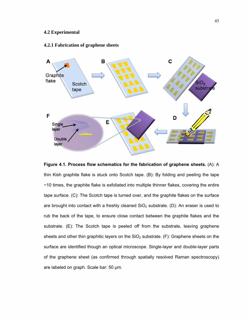
Figure 4.1. Process flow schematics for the fabrication of graphene sheets. (A): A
thin Kish graphite flake is stuck onto Scotch tape. (B): By folding and peeling the tape
~10 times, the graphite flake is exfoliated into multiple thinner flakes, covering the entire
tape surface. (C): The Scotch tape is turned over, and the graphite flakes on the surface
are brought into contact with a freshly cleaned SiO2 substrate. (D): An eraser is used to
rub the back of the tape, to ensure close contact between the graphite flakes and the
substrate. (E): The Scotch tape is peeled off from the substrate, leaving graphene
sheets and other thin graphitic layers on the SiO2 substrate. (F): Graphene sheets on the
surface are identified though an optical microscope. Single-layer and double-layer parts
of the graphene sheet (as confirmed through spatially resolved Raman spectroscopy)
are labeled on graph. Scale bar: 50 µm.
46
The monolayer graphene sheets investigated in this study were fabricated on
insulating SiO2 substrates through mechanical exfoliation of Kish graphite flakes.3, 33 The
detailed process flow is presented in Figure 4.1. It should be noted that this process is
time-consuming and low-yielding, and the locations of the resultant graphene sheets are
uncontrolled.
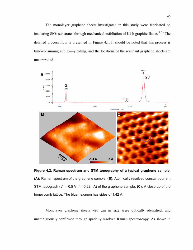
Figure 4.2. Raman spectrum and STM topography of a typical graphene sample.
(A): Raman spectrum of the graphene sample. (B): Atomically resolved constant-current
STM topograph (Vb = 0.5 V, I = 0.22 nA) of the graphene sample. (C): A close-up of the
honeycomb lattice. The blue hexagon has sides of 1.42 Å.
Monolayer graphene sheets ~20 µm in size were optically identified, and
unambiguously confirmed through spatially resolved Raman spectroscopy. As shown in
47
Figure 4.2A, a symmetric single peak is observed at ~2700 cm-1 (2D band) in the Raman
spectrum, and the peak height is larger than the G band at ~1580 cm-1. Both features are
characteristic of pristine monolayer graphene sheets.34, 35 Ti/Au electrodes were contacted
to the fabricated graphene sheets using electron-beam lithography, and Hall
measurements revealed room-temperature carrier mobilities of >6,000 cm2/Vs, which is
typical of high-quality graphene at room temperature.4
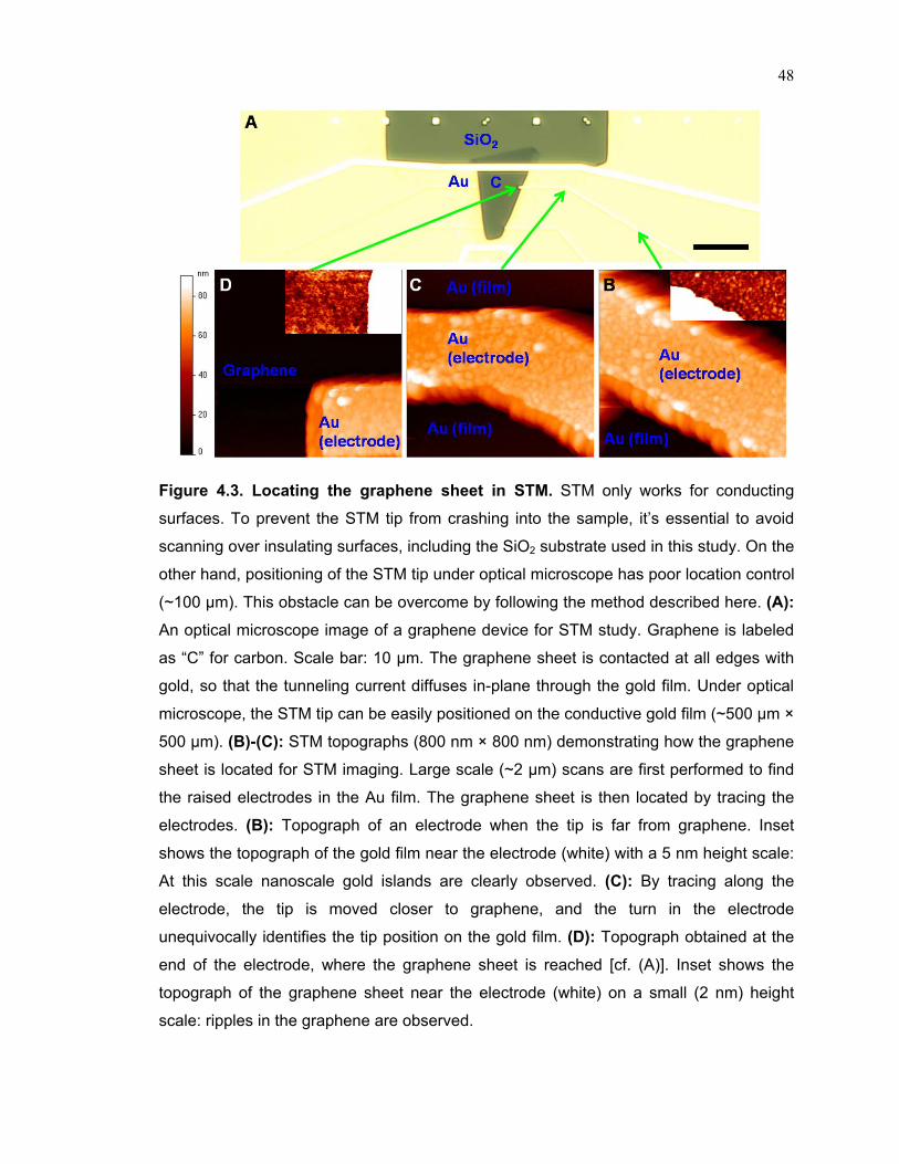
For STM measurements, the graphene sheets were then contacted at all edges
with gold, so that the tunneling current diffused in-plane through the gold film. The
electrodes defined in the previous step served as guides for locating the graphene sheets
using STM (Figure 4.3). As in previous chapters, STM studies were performed using an
Omicron low-temperature UHV STM system with mechanically cut Pt/Ir tips. All STM
data were taken at liquid nitrogen (77 K) or liquid helium (4 K) temperatures, and a
vacuum of better than 10-10 Torr was maintained during experiment.
4.2.2 Fabrication of graphene nanoribbons
Our GNR devices were prepared using a superlattice nanowire pattern (SNAP)
transfer technique.36 SNAP uses a template consisting of alternating layers of
GaAs/AlxGa(1-x)As, which is grown by molecular-beam epitaxy (MBE) on top of GaAs
wafers, for nanowire (NW) patterning. Through selective etching of either GaAs or
AlxGa(1-x)As, layer thickness can be translated to the nanowire width. In principle, this
width can be as thin as a few atomic layers since MBE is capable of growing with atomic
resolution.
48
Figure 4.3. Locating the graphene sheet in STM. STM only works for conducting
surfaces. To prevent the STM tip from crashing into the sample, it’s essential to avoid
scanning over insulating surfaces, including the SiO2 substrate used in this study. On the
other hand, positioning of the STM tip under optical microscope has poor location control
(~100 µm). This obstacle can be overcome by following the method described here. (A):
An optical microscope image of a graphene device for STM study. Graphene is labeled
as “C” for carbon. Scale bar: 10 µm. The graphene sheet is contacted at all edges with
gold, so that the tunneling current diffuses in-plane through the gold film. Under optical
microscope, the STM tip can be easily positioned on the conductive gold film (~500 µm ×
500 µm). (B)-(C): STM topographs (800 nm × 800 nm) demonstrating how the graphene
sheet is located for STM imaging. Large scale (~2 µm) scans are first performed to find
the raised electrodes in the Au film. The graphene sheet is then located by tracing the
electrodes. (B): Topograph of an electrode when the tip is far from graphene. Inset
shows the topograph of the gold film near the electrode (white) with a 5 nm height scale:
At this scale nanoscale gold islands are clearly observed. (C): By tracing along the
electrode, the tip is moved closer to graphene, and the turn in the electrode
unequivocally identifies the tip position on the gold film. (D): Topograph obtained at the
end of the electrode, where the graphene sheet is reached [cf. (A)]. Inset shows the
topograph of the graphene sheet near the electrode (white) on a small (2 nm) height
scale: ripples in the graphene are observed.
49
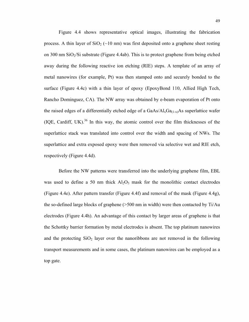
Figure 4.4 shows representative optical images, illustrating the fabrication
process. A thin layer of SiO2 (~10 nm) was first deposited onto a graphene sheet resting
on 300 nm SiO2/Si substrate (Figure 4.4ab). This is to protect graphene from being etched
away during the following reactive ion etching (RIE) steps. A template of an array of
metal nanowires (for example, Pt) was then stamped onto and securely bonded to the
surface (Figure 4.4c) with a thin layer of epoxy (EpoxyBond 110, Allied High Tech,
Rancho Dominguez, CA). The NW array was obtained by e-beam evaporation of Pt onto
the raised edges of a differentially etched edge of a GaAs/AlxGa(1-x)As superlattice wafer
(IQE, Cardiff, UK).36 In this way, the atomic control over the film thicknesses of the
superlattice stack was translated into control over the width and spacing of NWs. The
superlattice and extra exposed epoxy were then removed via selective wet and RIE etch,
respectively (Figure 4.4d).
Before the NW patterns were transferred into the underlying graphene film, EBL
was used to define a 50 nm thick Al2O3 mask for the monolithic contact electrodes
(Figure 4.4e). After pattern transfer (Figure 4.4f) and removal of the mask (Figure 4.4g),
the so-defined large blocks of graphene (>500 nm in width) were then contacted by Ti/Au
electrodes (Figure 4.4h). An advantage of this contact by larger areas of graphene is that
the Schottky barrier formation by metal electrodes is absent. The top platinum nanowires
and the protecting SiO2 layer over the nanoribbons are not removed in the following
transport measurements and in some cases, the platinum nanowires can be employed as a
top gate.
50
Figure 4.4. Representative bright-field optical images following the GNR
fabrication process. (a) Exfoliated graphene on 300 nm SiO2/Si substrate. (b)
Evaporation of 18 nm SiO2 protection layer, covering both graphene and substrate. (c)
Stamping of SNAP Pt nanowires onto graphene via epoxy bonding. (d) Extra epoxy in
between nanowires removed by RIE in a 40 MHz Unaxis SLR parallel-plate RIE system
~5 min with O2 (10 sccm, 5 mTorr, 40 W). (e) Evaporation of 50 nm thick Al2O3 mask to
define the monolithic contacts. Spacings between the masks were adjusted so as to
define GNRs of different lengths (ranging from 0.5 to ~50 µm) but of the same width. (f)
Both nanoribbon and electrode patterns were transferred into the graphene film.
Exposed SiO2 and underlying graphene (not protected by Al2O3 mask and Pt nanowires)
were removed sequentially by highly directional RIE with ~4 min CF4/He (20/30 sccm, 5
mTorr, 40 W) and with ~2 min O2 plasma (10 sccm, 5 mTorr, 40W). (g) Al2O3 Mask
removed by ~30 minutes in 10% H3PO4 + 90% H2O. (h) Evaporation of Ti/Au (20/200
nm) to make metal contacts. The scale bar is 10 μm and applies for all images.
a b
c
e
d
g
f
h
51
The conductance of GNRs was measured using a standard lock-in technique. A
low-noise function generator (DS360, Stanford Research System) was used to supply an
AC signal (100 µV at 11 Hz) to the device and the output signal was fed into a lock-in
amplifier (SR830, Stanford Research System). The time constant and slope used in the
experiments were 300 ms and 12 dB, respectively. The heavily doped silicon substrate
below the 300 nm SiO2 served as a bottom gate electrode to tune the carrier density in the
GNRs. The gate voltages were supplied by a Keithley 2400 source meter. Temperature-
dependent experiments were carried out in a SQUID cryostat (MPMS-XL, Quantum
Design, CA). A program written with Labview 7.1 was used to control the operations.
4.3 Structural and electrical characterizations of graphene wrinkles
Figure 4.2B gives the constant-current STM topograph obtained from a typical
graphene device. Atomically resolved, clear honeycomb structures were observed for all
samples, with bond lengths in agreement with the known graphene lattice constant
(Figure 4.2C). The same honeycomb structures are obtained independent of the specific
parameters used for imaging.
No lattice defects were ever observed during our atomically resolved STM study
over an accumulated area of ~104 nm2 on different samples, corresponding to >105 atoms.
This is in agreement with the measured high carrier mobilities, but in contrast with STM
results obtained on graphene epitaxially grown on conductive substrates, in which lattice
defects are observed at the nanometer scale.37 Surface corrugations (ripples) of ~4 Å in
height are observed for most regions of our graphene samples (Figure 4.2B), in
agreement with previous studies.17-21
52
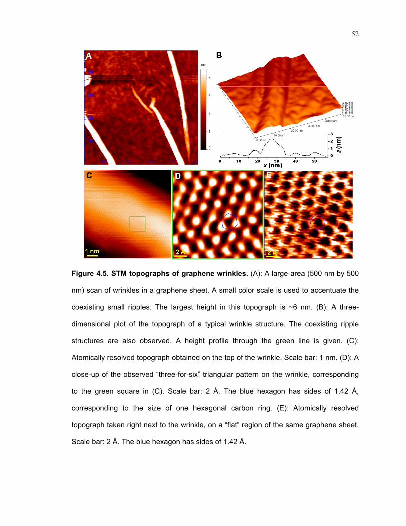
Figure 4.5. STM topographs of graphene wrinkles. (A): A large-area (500 nm by 500
nm) scan of wrinkles in a graphene sheet. A small color scale is used to accentuate the
coexisting small ripples. The largest height in this topograph is ~6 nm. (B): A three-
dimensional plot of the topograph of a typical wrinkle structure. The coexisting ripple
structures are also observed. A height profile through the green line is given. (C):
Atomically resolved topograph obtained on the top of the wrinkle. Scale bar: 1 nm. (D): A
close-up of the observed “three-for-six” triangular pattern on the wrinkle, corresponding
to the green square in (C). Scale bar: 2 Å. The blue hexagon has sides of 1.42 Å,
corresponding to the size of one hexagonal carbon ring. (E): Atomically resolved
topograph taken right next to the wrinkle, on a “flat” region of the same graphene sheet.
Scale bar: 2 Å. The blue hexagon has sides of 1.42 Å.
53
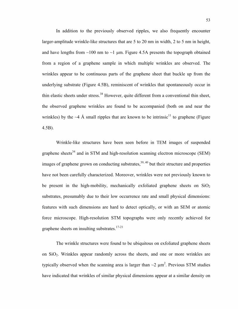
In addition to the previously observed ripples, we also frequently encounter
larger-amplitude wrinkle-like structures that are 5 to 20 nm in width, 2 to 5 nm in height,
and have lengths from ~100 nm to ~1 µm. Figure 4.5A presents the topograph obtained
from a region of a graphene sample in which multiple wrinkles are observed. The
wrinkles appear to be continuous parts of the graphene sheet that buckle up from the
underlying substrate (Figure 4.5B), reminiscent of wrinkles that spontaneously occur in
thin elastic sheets under stress.38 However, quite different from a conventional thin sheet,
the observed graphene wrinkles are found to be accompanied (both on and near the
wrinkles) by the ~4 Å small ripples that are known to be intrinsic11 to graphene (Figure
4.5B).
Wrinkle-like structures have been seen before in TEM images of suspended
graphene sheets34 and in STM and high-resolution scanning electron microscope (SEM)
images of graphene grown on conducting substrates,39, 40 but their structure and properties
have not been carefully characterized. Moreover, wrinkles were not previously known to
be present in the high-mobility, mechanically exfoliated graphene sheets on SiO2
substrates, presumably due to their low occurrence rate and small physical dimensions:
features with such dimensions are hard to detect optically, or with an SEM or atomic
force microscope. High-resolution STM topographs were only recently achieved for
graphene sheets on insulting substrates.17-21
The wrinkle structures were found to be ubiquitous on exfoliated graphene sheets
on SiO2. Wrinkles appear randomly across the sheets, and one or more wrinkles are
typically observed when the scanning area is larger than ~2 µm2. Previous STM studies
have indicated that wrinkles of similar physical dimensions appear at a similar density on
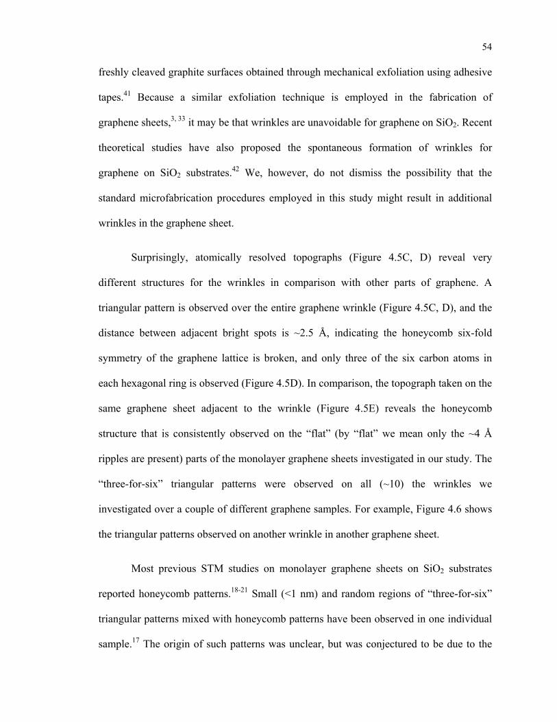
54
freshly cleaved graphite surfaces obtained through mechanical exfoliation using adhesive
tapes.41 Because a similar exfoliation technique is employed in the fabrication of
graphene sheets,3, 33 it may be that wrinkles are unavoidable for graphene on SiO2. Recent
theoretical studies have also proposed the spontaneous formation of wrinkles for
graphene on SiO2 substrates.42 We, however, do not dismiss the possibility that the
standard microfabrication procedures employed in this study might result in additional
wrinkles in the graphene sheet.
Surprisingly, atomically resolved topographs (Figure 4.5C, D) reveal very
different structures for the wrinkles in comparison with other parts of graphene. A
triangular pattern is observed over the entire graphene wrinkle (Figure 4.5C, D), and the
distance between adjacent bright spots is ~2.5 Å, indicating the honeycomb six-fold
symmetry of the graphene lattice is broken, and only three of the six carbon atoms in
each hexagonal ring is observed (Figure 4.5D). In comparison, the topograph taken on the
same graphene sheet adjacent to the wrinkle (Figure 4.5E) reveals the honeycomb
structure that is consistently observed on the “flat” (by “flat” we mean only the ~4 Å
ripples are present) parts of the monolayer graphene sheets investigated in our study. The
“three-for-six” triangular patterns were observed on all (~10) the wrinkles we
investigated over a couple of different graphene samples. For example, Figure 4.6 shows
the triangular patterns observed on another wrinkle in another graphene sheet.
Most previous STM studies on monolayer graphene sheets on SiO2 substrates
reported honeycomb patterns.18-21 Small (<1 nm) and random regions of “three-for-six”
triangular patterns mixed with honeycomb patterns have been observed in one individual
sample.17 The origin of such patterns was unclear, but was conjectured to be due to the
55
presence of “strong spatially dependent perturbations”, including local curvature or
trapped charges.17, 43 In our study, honeycomb patterns are observed for all “flat” parts of
graphene (with ~4 Å high ripples), while triangular patterns are exclusively and
consistently observed on the ~3 nm high wrinkles. These results indicate that increased
local curvature (and the associated strain) on the wrinkles can provide strong enough
perturbations to break the six-fold symmetry and degeneracy of the electronic states in
graphene.
Because STM topographs represent the local density of states (DOS) distribution,
we were able to further investigate how the “three-for-six” pattern characteristic of the
wrinkles reflected the local electronic states and geometric structure of graphene.44 This
can be probed by measuring topographs at both positive and negative sample biases,44
since such STM measurements will respectively probe the LUMO (empty states) and
HOMO (filled states) of the sample.
Figure 4.6A, B gives the atomically resolved STM topographs of the top surface
of a graphene wrinkle, obtained at positive and negative sample biases. The same “three-
for-six” triangular patterns are observed for positive and negative biases (Figure 4.6C):
the center parts of the two topographs, which correspond to the crest of the wrinkle,
overlap with each other exactly, and a regular triangular lattice is observed. Small
distortions of the triangular lattice are observed for regions away from the center, and the
patterns obtained from the two scans gradually mismatch with each other. This suggests
that the wrinkle is flexible, and the force from the STM tip causes a slight deformation of
the wrinkle during scans. In comparison, on the “flat” part of the same graphene sheet
(Figure 4.6D-F), although ~4 Å ripples are present, clear honeycomb structures were
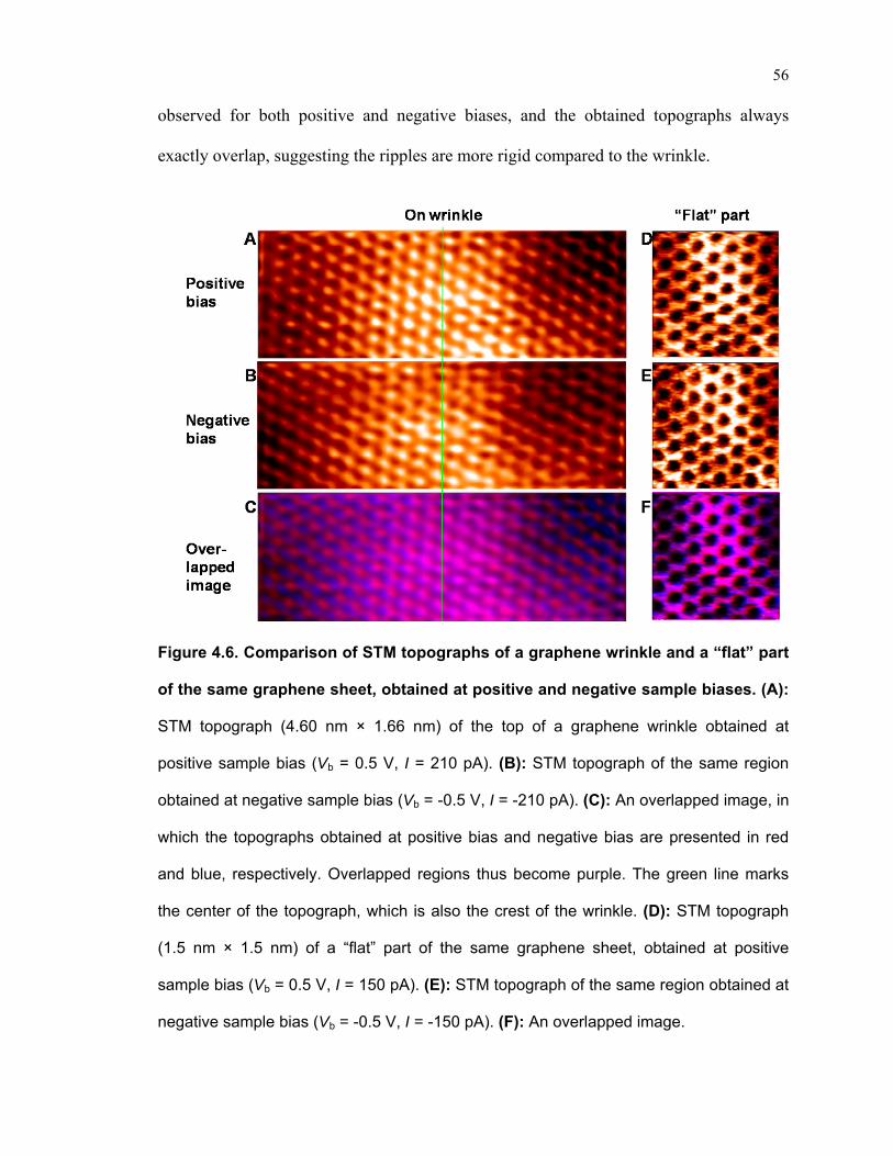
56
observed for both positive and negative biases, and the obtained topographs always
exactly overlap, suggesting the ripples are more rigid compared to the wrinkle.
Figure 4.6. Comparison of STM topographs of a graphene wrinkle and a “flat” part
of the same graphene sheet, obtained at positive and negative sample biases. (A):
STM topograph (4.60 nm × 1.66 nm) of the top of a graphene wrinkle obtained at
positive sample bias (Vb = 0.5 V, I = 210 pA). (B): STM topograph of the same region
obtained at negative sample bias (Vb = -0.5 V, I = -210 pA). (C): An overlapped image, in
which the topographs obtained at positive bias and negative bias are presented in red
and blue, respectively. Overlapped regions thus become purple. The green line marks
the center of the topograph, which is also the crest of the wrinkle. (D): STM topograph
(1.5 nm × 1.5 nm) of a “flat” part of the same graphene sheet, obtained at positive
sample bias (Vb = 0.5 V, I = 150 pA). (E): STM topograph of the same region obtained at
negative sample bias (Vb = -0.5 V, I = -150 pA). (F): An overlapped image.
57
The same “three-for-six” patterns obtained on the wrinkle at positive and negative
sample biases suggest the patterns reflect the actual topology of atoms in graphene.
Recent experiments on hydrogenation of graphene have suggested that local
bending/curvature in graphene may induce some sp3 hybridization component in the
otherwise sp2-hybridized carbons, which facilitates the breaking of delocalized π-bonds
in graphene.45, 46 With a tendency towards sp3 hybridization, the six carbon atoms in each
hexagon ring of graphene may start to adopt a structure similar to the chair conformation
of cyclohexane, and so three of the six atoms protrude up and out of the hexagon ring,
leading to the “three-for-six” pattern seen in our STM topographs.
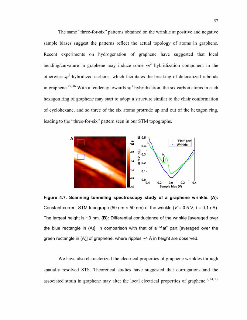
Figure 4.7. Scanning tunneling spectroscopy study of a graphene wrinkle. (A):
Constant-current STM topograph (50 nm × 50 nm) of the wrinkle (V = 0.5 V, I = 0.1 nA).
The largest height is ~3 nm. (B): Differential conductance of the wrinkle [averaged over
the blue rectangle in (A)], in comparison with that of a “flat” part [averaged over the
green rectangle in (A)] of graphene, where ripples ~4 Å in height are observed.
We have also characterized the electrical properties of graphene wrinkles through
spatially resolved STS. Theoretical studies have suggested that corrugations and the
associated strain in graphene may alter the local electrical properties of graphene.5, 14, 15
BA
-0.4 -0.2 0.0 0.2 0.40.0
0.1
0.2
0.3
0.4
0.5d
I /d
V (
nS
)
Sample bias (V)
"Flat" part Wrinkle
VD
58
On the other hand, recent STS studies on graphene have found very limited or no
correlations between corrugations and local electrical properties.21-23 This is presumably
because the previously studied ripples on “flat” parts of graphene were too small (~4 Å in
height).
We have found distinctly different electrical properties for the ~3 nm high
wrinkles. Figure 4.7B presents the differential conductance behavior of a wrinkle, in
comparison with other parts of the graphene sheet, where small ripples are present.
Lower conductance is observed for the wrinkle at low bias voltages, indicating the
wrinkle is less conductive than other parts of graphene. This is in agreement with our
previous discussions that the local bending/curvature effects may weaken delocalized π-
bonds. For the “flat” part of graphene, in addition to a soft gap at zero bias, a clear dip
(local minimum) of differential conductance is observed at VD = -0.12 V (Figure 4.7B).
This corresponds to the charge-neutral Dirac point of graphene,19 at which energy the
conduction and valance bands of graphene meet at a single point in k-space, and so
charge carriers vanish. Interestingly, this dip disappears on the wrinkle (Fig 4.7B). This
may be explained with recent theoretical studies, which suggest large local corrugations
may lead to midgap states, and so a finite density of state is present at the neutrality
point.14, 46, 47
We have utilized cryo-STM to investigate a new class of corrugations in
monolayer graphene sheets, i.e., wrinkles ~10 nm in width and ~3 nm in height. We
found such corrugations to be ubiquitous in graphene and have distinctly different
properties in comparison to “flat” regions of graphene that only contain small ripples.
The observed wrinkles are likely important for understanding the electrical and
59
mechanical properties of graphene. Recently developed graphene manipulation
methods48, 49 may permit the controlled formation of wrinkles, which would be a first step
toward harnessing wrinkles to control the electronic landscape of graphene sheets.
4.4 Electron transport in graphene nanoribbons
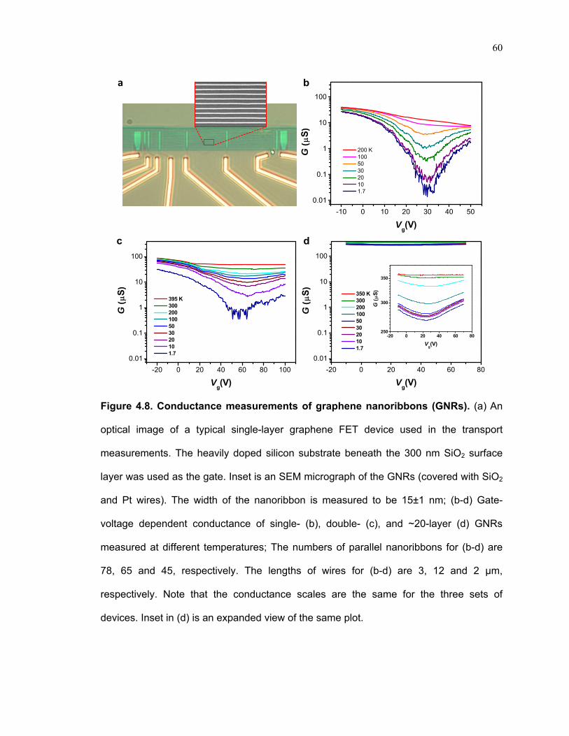
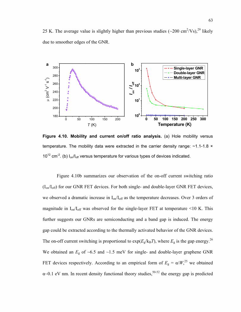
Figure 4.8 summarizes the conductance measurements as a function of gate
voltage for three representative GNR devices of varying numbers of graphene layers (1, 2
and ~20) but the same uniform width (W = 15±1 nm). In our experiments, a heavily
doped silicon substrate beneath the 300 nm SiO2 surface layer was employed as the back
gate. The measurements were performed at different temperatures as indicated. All
curves exhibit a region of depressed conductance with respect to the gate voltage. As
mentioned above, the carrier density in graphene vanishes at the Dirac point, where the
conductance and valence bands meet. It is then expected in a low carrier density system
that a dip in conductance would occur while tuning the carrier density by gating.27 In an
ideal, undoped device, this should occur at zero gate voltages. In our experiments,
however, we often observe different minimal-conductance positions for different devices.
Even for the same device, temperature cycling also often induces shifting of the minimal-
conductance points and thus hysteresis. These shifts of the observed minimal-
conductance points are due to the charges trapped in the underlying SiO2 and possible
adsorbates on top of graphene, which act as an electrostatic gate and modify the carrier
types and densities accordingly.23 For most of our devices, the minimal-conductance
point occurs at positive gate voltages, indicating that they are p-type.
60
Figure 4.8. Conductance measurements of graphene nanoribbons (GNRs). (a) An
optical image of a typical single-layer graphene FET device used in the transport
measurements. The heavily doped silicon substrate beneath the 300 nm SiO2 surface
layer was used as the gate. Inset is an SEM micrograph of the GNRs (covered with SiO2
and Pt wires). The width of the nanoribbon is measured to be 15±1 nm; (b-d) Gate-
voltage dependent conductance of single- (b), double- (c), and ~20-layer (d) GNRs
measured at different temperatures; The numbers of parallel nanoribbons for (b-d) are
78, 65 and 45, respectively. The lengths of wires for (b-d) are 3, 12 and 2 µm,
respectively. Note that the conductance scales are the same for the three sets of
devices. Inset in (d) is an expanded view of the same plot.
-20 0 20 40 60 80250
300
350
G (S
)
Vg(V)
-20 0 20 40 60 80
0.01
0.1
1
10
100
G (S
)
Vg(V)
350 K 300 200 100 50 30 20 10 1.7
-10 0 10 20 30 40 50
0.01
0.1
1
10
100
G (S
)
Vg(V)
200 K 100 50 30 20 10 1.7
-20 0 20 40 60 80 100
0.01
0.1
1
10
100
G (S
)
Vg(V)
395 K 300 200 100 50 30 20 10 1.7
b
c d
a
61
Our observations of a depressed region of conductance in GNRs are qualitatively
in agreement with that in graphene films.25 In “bulk” graphene, this dip corresponds to
the minimum conductivity ~4e2/h, where e and h are electron charge and Planck constant,
respectively. At higher temperatures (>200K), a similar behavior is observed in our GNR
devices. For instance, at room temperature the single-layer GNR device gives a
conductance dip (data not shown here) on the order of 4e2/h(nW/L), where n and L are the
number and length of parallel GNRs, respectively.
Remarkably, at low temperatures the minimum conductance decreases by more
than an order of magnitude for both single- and double-layer GNRs, whereas the multi-
layer device exhibits small decreases (Figure 4.8b-d). These results, i.e., conductance
decreases with decreasing temperature regardless of the number of layers, indicate
thermally activated behavior. This observed behavior is in general agreement with
previous studies on individual GNRs, and suggests the opening up of band gaps in GNRs.
In contrast, the conductance of bulk graphene films generally increases with decreasing
temperature. However, it is noteworthy that in our study, the conductance gaps smoothly
and consistently increase as temperature decreases for all GNR devices. This is in
contrast to the large, ill-defined variations typically observed in previous studies on
individual graphene nanoribbons.27, 29 This is likely because we are measuring parallel
GNRs, and so such sample-dependent variations are averaged out. Meanwhile, the more
meaningful general trend becomes much clearer.
As the number of graphene layers increases, the temperature and gate-voltage
dependence of conductance both weakens, suggesting smaller energy gaps in thicker
GNRs. For the ~20 layer GNRs in our study, the gap practically vanishes. This clear
62
observation that the band gap (and so the on-off ratio) decreases as the number of layers
increases highlights the precisely controlled GNR width afforded by our SNAP technique.
In contrast, previous experiments have not been able to tell the property differences
between GNRs made of different numbers of layers, due to the difficulties in obtaining
GNRs of well-defined widths.
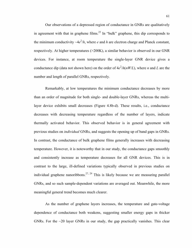
Figure 4.9. Linear dependence of GNR resistance on ribbon length. A plot of the
resistance of single-layer graphene nanoribbons versus length, measured at room
temperature with zero back-gate voltage. The number of ribbons in parallel is 78. Similar
linear relationships were also observed for double- and multi-layer GNRs.
Figure 4.9 shows the total resistance of GNR arrays as a function of GNR length.
A clear linear dependence is observed, which highlights the high quality of our GNRs
with uniform properties. The small nonzero resistance at zero GNR length is likely due to
the residue contact resistance which is independent of the ribbon length and can be
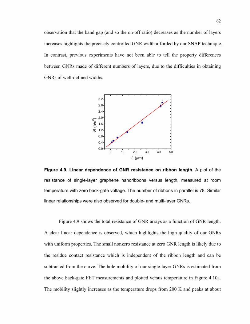
subtracted from the curve. The hole mobility of our single-layer GNRs is estimated from
the above back-gate FET measurements and plotted versus temperature in Figure 4.10a.
The mobility slightly increases as the temperature drops from 200 K and peaks at about
0 10 20 30 40 500.0
0.4
0.8
1.2
1.6
2.0
2.4
2.8
3.2R
(h/
e2 )
L (m)
63
25 K. The average value is slightly higher than previous studies (~200 cm2/Vs),29 likely
due to smoother edges of the GNR.
Figure 4.10. Mobility and current on/off ratio analysis. (a) Hole mobility versus
temperature. The mobility data were extracted in the carrier density range: ~1.1-1.8 ×
1012 cm-2. (b) Ion/Ioff versus temperature for various types of devices indicated.
Figure 4.10b summarizes our observation of the on-off current switching ratio
(Ion/Ioff) for our GNR FET devices. For both single- and double-layer GNR FET devices,
we observed a dramatic increase in Ion/Ioff as the temperature decreases. Over 3 orders of
magnitude in Ion/Ioff was observed for the single-layer FET at temperature <10 K. This
further suggests our GNRs are semiconducting and a band gap is induced. The energy
gap could be extracted according to the thermally activated behavior of the GNR devices.
The on-off current switching is proportional to exp(Eg/kBT), where Eg is the gap energy.26
We obtained an Eg of ~6.5 and ~1.5 meV for single- and double-layer graphene GNR
FET devices respectively. According to an empirical form of Eg = α/W,25 we obtained
α~0.1 eV nm. In recent density functional theory studies,50-52 the energy gap is predicted
0 50 100 150 200180
200
220
240
260
280
300
(c
m2 V
-1 s
-1)
T (K)
0 50 100 150 200 250 300100
101
102
103 Single-layer GNR Double-layer GNR Multi-layer GNR
I on /
Io
ff
Temperature (K)
a b
64
to be inversely proportional to the ribbon channel width, with a corresponding α value
ranging from 0.2-1.5 eV nm, which is largely consistent with our observation.
4.5 Conclusion
In this chapter, we report on the scanning tunneling microscopy study of a new
class of corrugations in exfoliated monolayer graphene sheets, i.e., wrinkles ~10 nm in
width and ~3 nm in height. We found such corrugations to be ubiquitous in graphene, and
have distinctly different properties when compared to other regions of graphene. In
particular, a “three-for-six” triangular pattern of atoms is exclusively and consistently
observed on wrinkles, suggesting the local curvature of the wrinkle provides a sufficient
perturbation to break the six-fold symmetry of the graphene lattice. Through scanning
tunneling spectroscopy, we further demonstrate that the wrinkles have lower electrical
conductance and are characterized by the presence of midgap states, in agreement with
recent theoretical predictions. The observed wrinkles are likely important for
understanding the electrical properties of graphene.
We also studied the effect of width and number of graphene layers on the
electronic transport in graphene nanoribbons (GNRs). As the lateral size decreases to
nanometer range, conductance of all our GNR samples (regardless of number of layers)
shows thermally activated behavior. Noticeable conductance gaps open up in both single-
and double-layer GNR devices. The gaps smoothly and consistently increase as
temperature decreases for all GNR devices. This contrasts with bulk graphene films, the
conductance of which generally increases with decreasing temperature. Due to the
precisely controlled GNR width afforded by SNAP, we have also for the first time clearly
65
observed how the properties of GNRs evolve as a function of number of layers: the band
gap (and so the on-off ratio) decreases as the number of layers increases.
4.6 References
1. Xu, K., Cao, P.G. & Heath, J.R. Scanning tunneling microscopy characterization of the
electrical properties of wrinkles in exfoliated graphene monolayers. Nano Lett. 9, 4446-
4451 (2009).
2. Novoselov, K.S. et al. Electric field effect in atomically thin carbon films. Science 306,
666-669 (2004).
3. Novoselov, K.S. et al. Two-dimensional atomic crystals. Proc. Natl. Acad. Sci. U. S. A.
102, 10451-10453 (2005).
4. Geim, A.K. & Novoselov, K.S. The rise of graphene. Nat. Mater. 6, 183-191 (2007).
5. Neto, A.H.C., Guinea, F., Peres, N.M.R., Novoselov, K.S. & Geim, A.K. The electronic
properties of graphene. Rev. Mod. Phys. 81, 109-162 (2009).
6. Geim, A.K. Graphene: status and prospects. Science 324, 1530-1534 (2009).
7. Novoselov, K.S. et al. Room-temperature quantum hall effect in graphene. Science 315,
1379-1379 (2007).
8. Mermin, N.D. Crystalline order in two dimensions. Physical Review 176, 250-254
(1968).
9. Meyer, J.C. et al. The structure of suspended graphene sheets. Nature 446, 60-63 (2007).
10. Meyer, J.C. et al. On the roughness of single- and bi-layer graphene membranes. Solid
State Commun. 143, 101-109 (2007).
11. Fasolino, A., Los, J.H. & Katsnelson, M.I. Intrinsic ripples in graphene. Nat. Mater. 6,
858-861 (2007).
12. Morozov, S.V. et al. Strong suppression of weak localization in graphene. Phys Rev Lett
97, 016801 (2006).
13. Morozov, S.V. et al. Giant intrinsic carrier mobilities in graphene and its bilayer. Phys
Rev Lett 100, 016602 (2008).
14. Guinea, F., Katsnelson, M.I. & Vozmediano, M.A.H. Midgap states and charge
inhomogeneities in corrugated graphene. Phys Rev B 77, 075422 (2008).
15. Kim, E.A. & Neto, A.H.C. Graphene as an electronic membrane. Epl 84, 57007 (2008).
16. Herbut, I.F., Juricic, V. & Vafek, O. Coulomb interaction, ripples, and the minimal
conductivity of graphene. Phys Rev Lett 100, 046403 (2008).
66
17. Ishigami, M., Chen, J.H., Cullen, W.G., Fuhrer, M.S. & Williams, E.D. Atomic structure
of graphene on SiO2. Nano Lett. 7, 1643-1648 (2007).
18. Stolyarova, E. et al. High-resolution scanning tunneling microscopy imaging of
mesoscopic graphene sheets on an insulating surface. Proc. Natl. Acad. Sci. U. S. A. 104,
9209-9212 (2007).
19. Zhang, Y.B. et al. Giant phonon-induced conductance in scanning tunnelling
spectroscopy of gate-tunable graphene. Nat. Phys. 4, 627-630 (2008).
20. Geringer, V. et al. Intrinsic and extrinsic corrugation of monolayer graphene deposited on
SiO2. Phys Rev Lett 102, 076102 (2009).
21. Deshpande, A., Bao, W., Miao, F., Lau, C.N. & LeRoy, B.J. Spatially resolved
spectroscopy of monolayer graphene on SiO2. Phys Rev B 79, 205411 (2009).
22. Teague, M.L. et al. Evidence for strain-induced local conductance modulations in single-
layer graphene on SiO2. Nano Lett. 9, 2542-2546 (2009).
23. Zhang, Y., Brar, V.W., Girit, C., Zettl, A. & Crommie, M.F. Origin of spatial charge
inhomogeneity in graphene. Nat. Phys. 5, 722-726 (2009).
24. Han, M.Y., Brant, J.C. & Kim, P. Electron transport in disordered graphene nanoribbons.
Phys Rev Lett 104, 056801 (2010).
25. Han, M.Y., Ozyilmaz, B., Zhang, Y.B. & Kim, P. Energy band-gap engineering of
graphene nanoribbons. Phys Rev Lett 98, 206805 (2007).
26. Li, X.L., Wang, X.R., Zhang, L., Lee, S.W. & Dai, H.J. Chemically derived, ultrasmooth
graphene nanoribbon semiconductors. Science 319, 1229-1232 (2008).
27. Chen, Z.H., Lin, Y.M., Rooks, M.J. & Avouris, P. Graphene nano-ribbon electronics.
Physica E 40, 228-232 (2007).
28. Jiao, L.Y., Zhang, L., Wang, X.R., Diankov, G. & Dai, H.J. Narrow graphene
nanoribbons from carbon nanotubes. Nature 458, 877-880 (2009).
29. Wang, X.R. et al. Room-temperature all-semiconducting sub-10-nm graphene nanoribbon
field-effect transistors. Phys Rev Lett 100, 206803 (2008).
30. Bai, J.W., Duan, X.F. & Huang, Y. Rational fabrication of graphene nanoribbons using a
nanowire etch mask. Nano Lett. 9, 2083-2087 (2009).
31. Sols, F., Guinea, F. & Neto, A.H.C. Coulomb blockade in graphene nanoribbons. Phys
Rev Lett 99, 166803 (2007).
32. Martin, I. & Blanter, Y.M. Transport in disordered graphene nanoribbons. Phys Rev B 79,
235132 (2009).
67
33. Zhang, Y.B., Tan, Y.W., Stormer, H.L. & Kim, P. Experimental observation of the
quantum Hall effect and Berry's phase in graphene. Nature 438, 201-204 (2005).
34. Ferrari, A.C. et al. Raman spectrum of graphene and graphene layers. Phys Rev Lett 97,
187401 (2006).
35. Graf, D. et al. Spatially resolved Raman spectroscopy of single- and few-layer graphene.
Nano Lett. 7, 238-242 (2007).
36. Melosh, N.A. et al. Ultrahigh-density nanowire lattices and circuits. Science 300, 112-
115 (2003).
37. Rutter, G.M. et al. Scattering and interference in epitaxial graphene. Science 317, 219-
222 (2007).
38. Cerda, E. & Mahadevan, L. Geometry and physics of wrinkling. Phys Rev Lett 90,
074302 (2003).
39. Biedermann, L.B., Bolen, M.L., Capano, M.A., Zemlyanov, D. & Reifenberger, R.G.
Insights into few-layer epitaxial graphene growth on 4H-SiC(0001) substrates from STM
studies. Phys Rev B 79, 125411 (2009).
40. Li, X.S. et al. Large-area synthesis of high-quality and uniform graphene films on copper
foils. Science 324, 1312-1314 (2009).
41. Chang, H.P. & Bard, A.J. Observation and characterization by scanning tunneling
microscopy of structures generated by cleaving highly oriented pyrolytic-graphite.
Langmuir 7, 1143-1153 (1991).
42. Guinea, F., Horovitz, B. & Le Doussal, P. Gauge fields, ripples and wrinkles in graphene
layers. Solid State Commun. 149, 1140-1143 (2009).
43. Stolyarova, E. et al. Scanning tunneling microscope studies of ultrathin graphitic
(graphene) films on an insulating substrate under ambient conditions. J Phys Chem C
112, 6681-6688 (2008).
44. Kane, C.L. & Mele, E.J. Broken symmetries in scanning tunneling images of carbon
nanotubes. Phys Rev B 59, R12759-R12762 (1999).
45. Ryu, S. et al. Reversible basal plane hydrogenation of graphene. Nano Lett. 8, 4597-4602
(2008).
46. Elias, D.C. et al. Control of graphene's properties by reversible hydrogenation: evidence
for graphane. Science 323, 610-613 (2009).
47. Wehling, T.O., Balatsky, A.V., Tsvelik, A.M., Katsnelson, M.I. & Lichtenstein, A.I.
Midgap states in corrugated graphene: Ab initio calculations and effective field theory.
Epl 84, 17003 (2008).
68
48. Bao, W. et al. Controlled ripple texturing of suspended graphene and ultrathin graphite
membranes. Nature Nanotechnology 4, 562-566 (2009).
49. Li, Z., Cheng, Z., Wang, R., Li, Q. & Fang, Y. Spontaneous formation of nanostructures
in graphene. Nano Lett. 9, 3599-3602 (2009).
50. Son, Y.W., Cohen, M.L. & Louie, S.G. Energy gaps in graphene nanoribbons. Phys Rev
Lett 97, 216803 (2006).
51. Son, Y.W., Cohen, M.L. & Louie, S.G. Half-metallic graphene nanoribbons. Nature 444,
347-349 (2006).
52. Barone, V., Hod, O. & Scuseria, G.E. Electronic structure and stability of semiconducting
graphene nanoribbons. Nano Lett. 6, 2748-2754 (2006).
Related Documents


