Chapter 12 Interfacing Analog and Digital Circuits

Welcome message from author
This document is posted to help you gain knowledge. Please leave a comment to let me know what you think about it! Share it to your friends and learn new things together.
Transcript

Chapter 12
Interfacing Analog and Digital Circuits

2
Analog Signals
• Signals that vary continuously throughout a defined range.
• Representative of many physical quantities, such as temperature and velocity.
• Usually a voltage or current level.

3
Digital Signals
• Signals that take on specific values only.
• Required for operation with digital logic.
• A representative of physical quantities by a series of binary numbers.

4
Advantages of Analog Representation
• Varies continuously, like the property being measured.
• Represents continuous values.
5
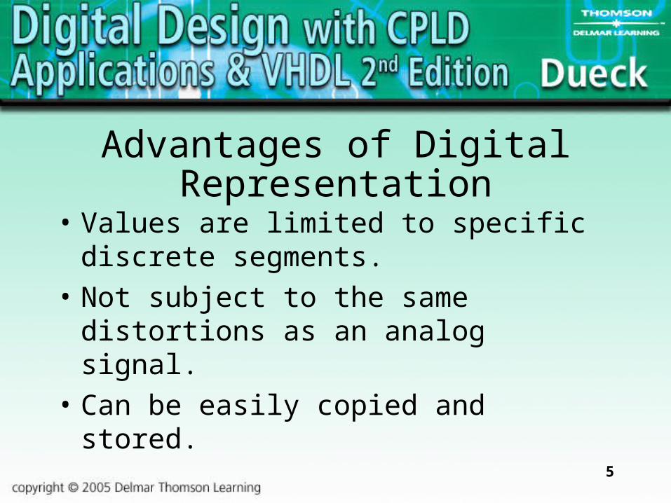
Advantages of Digital Representation
• Values are limited to specific discrete segments.
• Not subject to the same distortions as an analog signal.
• Can be easily copied and stored.

6
Advantages of Digital Representation

7
Analog Voltage Sampling
• A sample is an instantaneous measurement of an analog voltage.
• Sampling frequency is the number of samples taken per unit time.

8
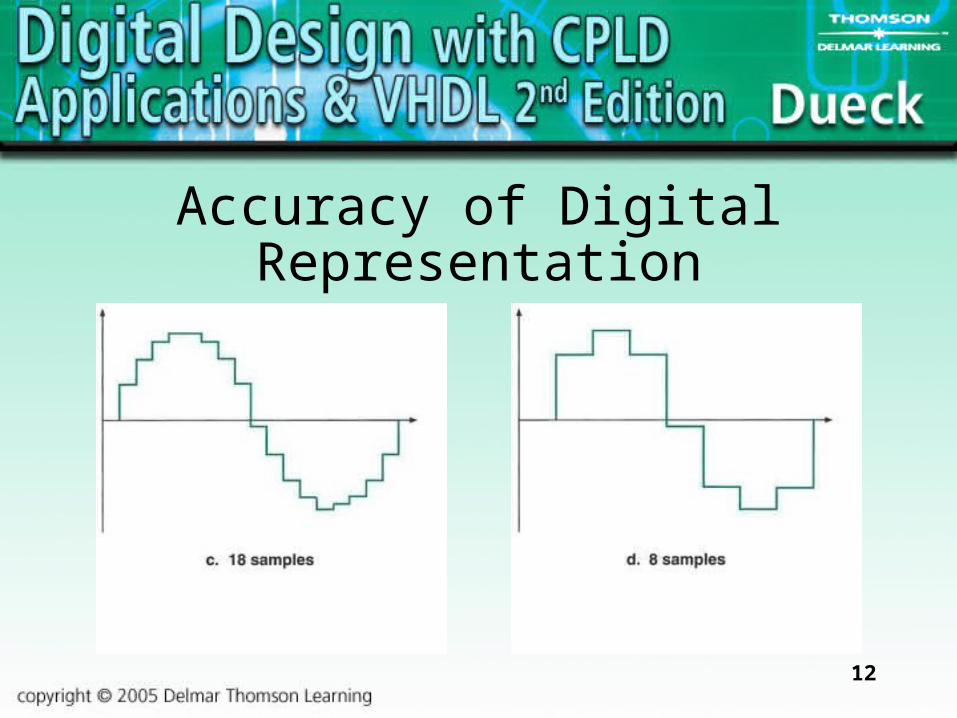
Accuracy of Digital Representation
• Depends on sampling frequency and quantization.
• Quantization is the number of bits used to represent an analog voltage as a digital number.
• Resolution is the analog step size.

9
Accuracy of Digital Representation

10
Accuracy of Digital Representation

11
Accuracy of Digital Representation
12
Accuracy of Digital Representation
13
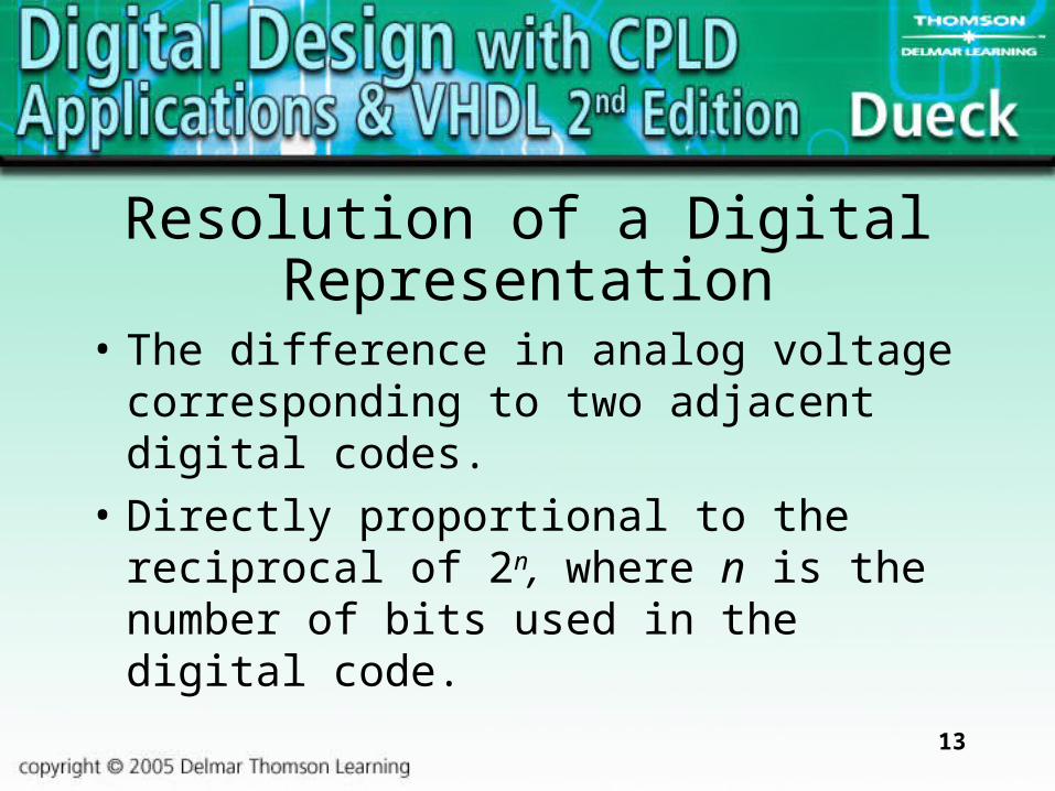
Resolution of a Digital Representation
• The difference in analog voltage corresponding to two adjacent digital codes.
• Directly proportional to the reciprocal of 2n, where n is the number of bits used in the digital code.

14
Analog-to-Digital Conversion
• Uses a circuit that converts an analog signal at its input to a digital code.
• Called an A-to-D converter, A/D converter, or ADC.

15
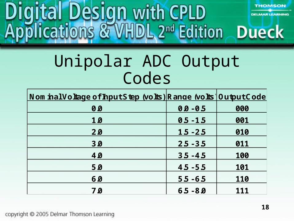
Unipolar ADC
• Converts positive input voltages.
• Generates a 2n-bit binary code for any given input voltage.

16
• Va = analog input voltage to be sampled.
• FS = Full scale range of input voltage.• n = number of bits in the output code.
n2 FS
V code a
Unipolar ADC Code Equation

17
Unipolar ADC Code Equation
18
Unipolar ADC Output Codes
Nominal Voltage of Input Step (volts) Range (volts) Output Code
0.0 0.0 - 0.5 000
1.0 0.5 - 1.5 001
2.0 1.5 - 2.5 010
3.0 2.5 - 3.5 011
4.0 3.5 - 4.5 100
5.0 4.5 - 5.5 101
6.0 5.5 - 6.5 110
7.0 6.5 - 8.0 111

19
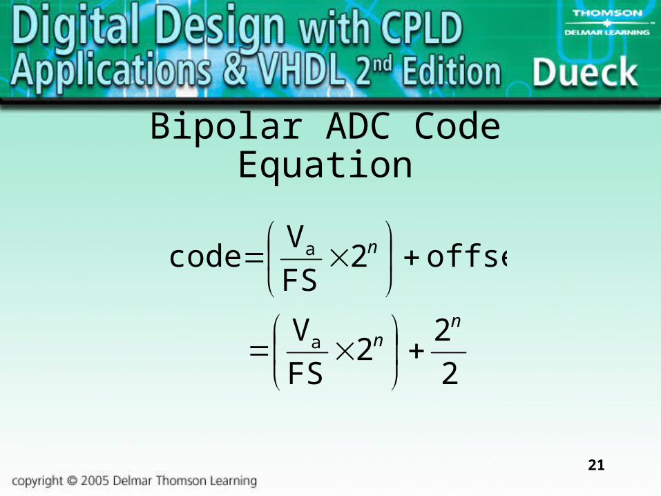
Bipolar ADC (Offset Binary Coding)
• Used to represent positive and negative input voltages.
• Output code an unsigned binary number.
• Numbers below 0 V are negative.
• Numbers above 0 V are positive.

20
Bipolar ADC (Offset Binary Coding)
21
Bipolar ADC Code Equation
2
22
FS
V
offset 2 FS
V code
a
a
nn
n

22
Bipolar ADC Output Codes
- 4.0 - 4.0 to - 3.5 000
- 3.0 - 3.5 to - 2.5 001
- 2.0 - 2.5 to - 1.5 010
- 1.0 - 1.5 to - 0.5 011
0 - 0.5 to + 0.5 100
+ 1.0 + 0.5 to + 1.5 101
+ 2.0 + 1.5 to + 2.5 110
+ 3.0 + 2.5 to + 4.0 111

23
Bipolar ADC (2’s Complement Coding)
• Uses a 2’s complement number system.
• Most significant bit (MSB) is the sign bit.
• MSB = ‘1’ sign negative.
• MSB = ‘0’ sign negative.

24
2’s Complement Output Codes
Nominal Voltage of Input Step (volts) Range (volts) Output Code
- 4.0 - 4.0 to - 3.5 100
- 3.0 - 3.5 to - 2.5 101
- 2.0 - 2.5 to - 1.5 110
- 1.0 - 1.5 to - 0.5 111
0 - 0.5 to + 0.5 000
+ 1.0 + 0.5 to + 1.5 001
+ 2.0 + 1.5 to + 2.5 010
+ 3.0 + 2.5 to + 4.0 011

25
2’s Complement Output Codes

26
Digital-to-Analog Conversion
• Uses a circuit that converts a digital code at its input to an analog voltage or current.
• Called a D-to-A converter, D/A converter, or DAC.

27
Unipolar DAC
• One input code corresponds to a single digital code.
• DAC has 2n discrete output voltage values.

28
Unipolar DAC

29
Unipolar DAC Equation
code bit- an for FS 2
codea nV
n

30
Bipolar DAC (Offset Binary Coding)
• Input code for 0 V is halfway through the range of digital input codes.
• Output voltage equation:
2
FS - FS
2
codea
nV
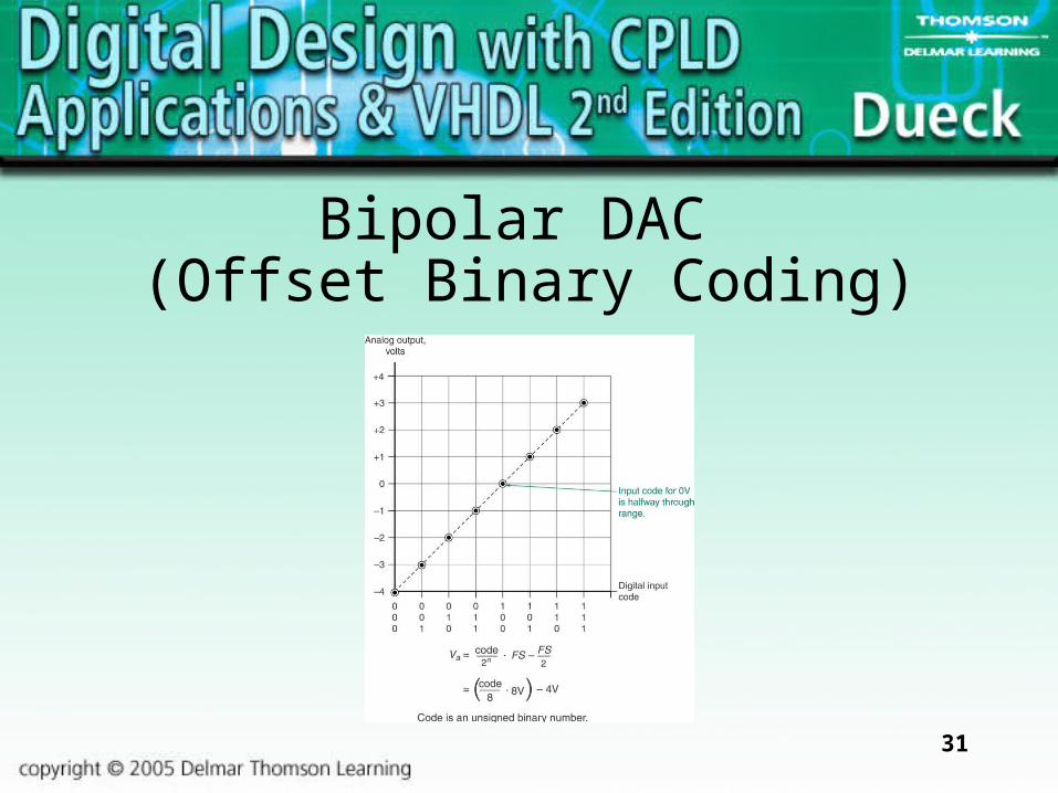
31
Bipolar DAC (Offset Binary Coding)
32
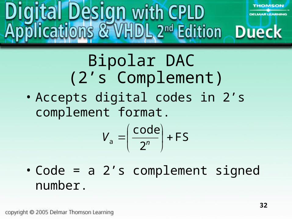
Bipolar DAC (2’s Complement)
• Accepts digital codes in 2’s complement format.
• Code = a 2’s complement signed number.
FS 2
code a
nV

33
Bipolar DAC (2’s Complement)
34
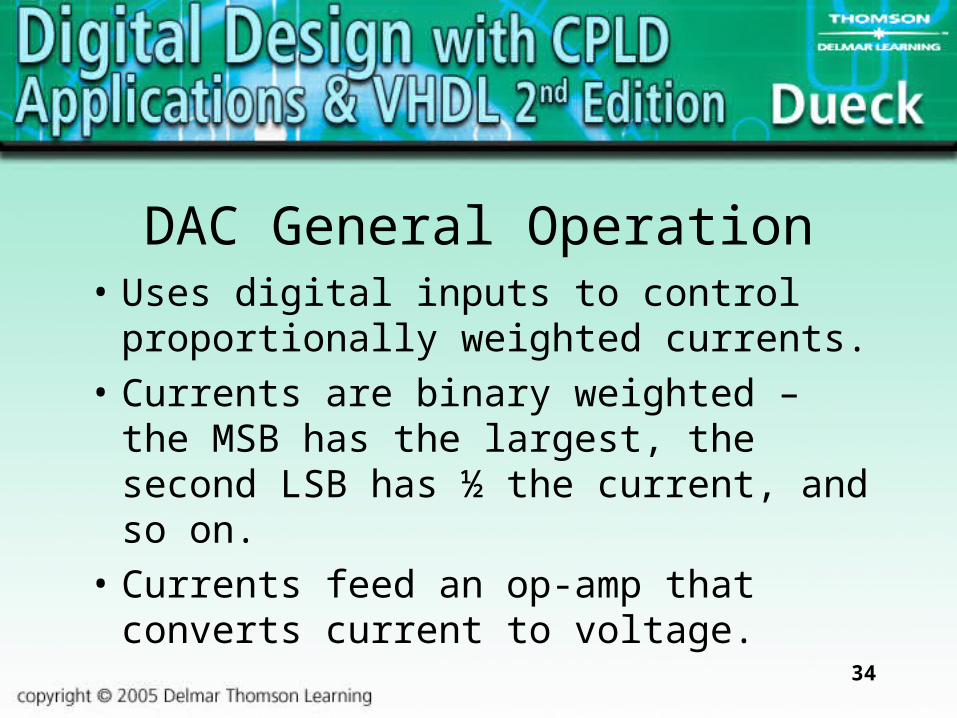
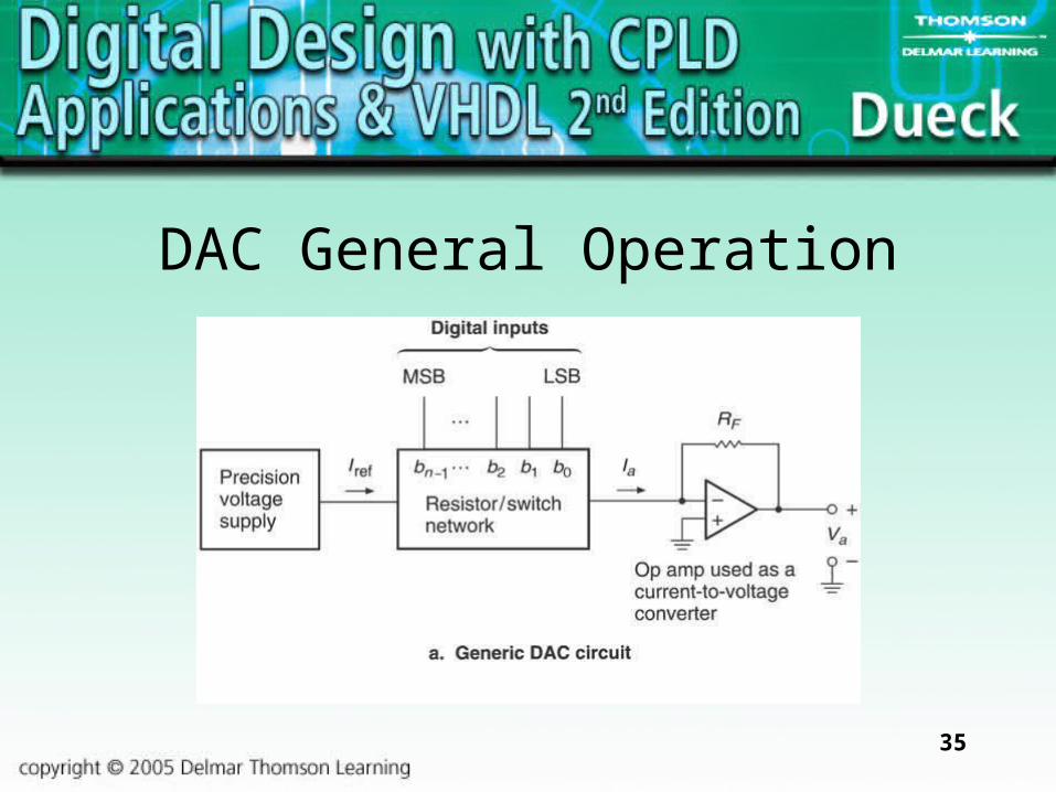
DAC General Operation• Uses digital inputs to control
proportionally weighted currents.
• Currents are binary weighted – the MSB has the largest, the second LSB has ½ the current, and so on.
• Currents feed an op-amp that converts current to voltage.
35
DAC General Operation

36
DAC Output Voltage
• If Va is the output, Iref a fixed reference current, and RF the op-amp feedback resistor, then for n bits:
refn
00
11
22
1-n1-n
a I2
2b2b2b...2b I

37
DAC Characteristics
• The maximum output is always one least significant bit less than full scale.
• An n-bit converter has 2n input codes, ranging from 0 to 2n – 1.

38
Weighted Resistor D/A Converter
• Uses a parallel network of binary-weighted resistors to feed the op-amp.
• Seldom used since a wide range of resistor values is required for a large number of bits.
• Difficult to achieve accuracy for a high number of bits.

39
Weighted Resistor D/A Converter

40
R-2R Ladder DAC
• Produces an analog current that is the sum of binary-weighted currents.
• Uses only two values of resistors.
• Easily modified to add additional bits – each new bit requires 2 resistors, values R and 2R.

41
R-2R Ladder DAC

42
• b3, b2, b1, and b0 are binary values either ‘1’ or ‘0’.
R-2R DAC Equation
ref0323
a 16842
Vbbbb
V

43
MC1408 Integrated Circuit DAC
• Popular, inexpensive 8-bit multiplying DAC.
• Also designated DAC0808.
• Output is proportional to the reference voltage.

44
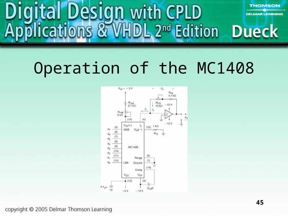
Operation of the MC1408
• Requires an external op-amp to increase the output voltage and current.
• Can be wired to produce a bipolar output voltage, that is, voltages that have both positive and negative values.
45
Operation of the MC1408

46
MC1408 Equations
ref14
FFOa
refO
14refref
256
code digital
256
code digital
)/(
VR
RRIV
II
RVI

47
DAC Performance Specifications – 1
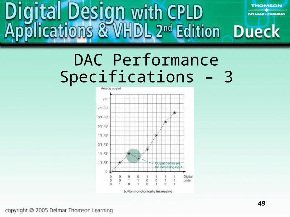
• Monotonicity means that the magnitude of the output voltage increases every time the input digital code increases.
• Absolute accuracy is the measure of the DAC output voltage with respect to its expected value.

48
DAC Performance Specifications – 2
49
DAC Performance Specifications – 3
50
DAC Performance Specifications – 4
• Relative accuracy is the deviation of the actual from the ideal output voltage as a fraction of the full-scale voltage.
• Settling time is the time required for the outputs to switch and settle within ½ LSB when the input switches form all 0s to all 1s.

51
DAC Performance Specifications – 5
• Gain error occurs when the output saturates before reaching the maximum output code.
• Linearity error is the deviation from a straight line output with increasing digital input codes.

52
DAC Performance Specifications – 6

53
DAC Performance Specifications – 7

54
DAC Performance Specifications – 8
• Differential nonlinearity is the difference between actual and expected step size when the input code is changed by 1 LSB.
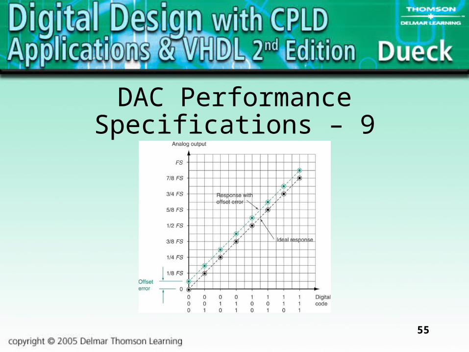
• Offset error occurs when the DAC output is not 0 V when the input code is all 0s.
55
DAC Performance Specifications – 9
56
Flash ADC
• Uses a resistive voltage divider, comparators, and a priority encoder to produce a digital code.
• Conversion occurs in one clock cycle (fastest conversion time).

57
Flash ADC

58
Flash ADC

59
Disadvantage of Flash ADC
• Requires 2n resistors and 2n – 1 comparators for an n-bit output.
• For any large number of bits, the circuit becomes overly complex.

60
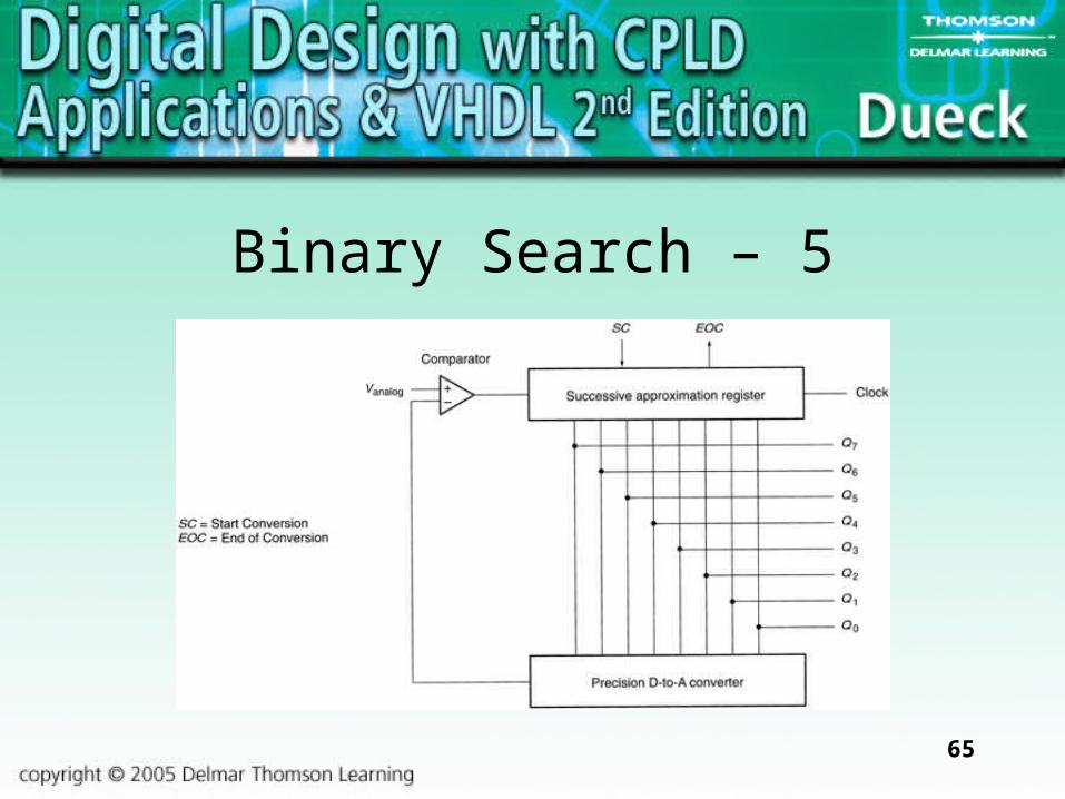
Successive Approximation ADC
• The most widely used ADC.
• Finds the digital representation using a “binary search.”
• Also called a SAR.

61
Binary Search – 1
1. Set the MSB of the digital representation to 1, all other bits to 0.
2. Compare the analog value produced in the first step to the voltage being converted.
2A. If the test voltage is higher than the voltage being converted, reset the MSB and set the second MSB.

62
Binary Search – 2
2B. If the test voltage is less than the voltage being converted, leave the MSB set and set the second MSB.
3. Repeat Steps 2, 2A, and 2B until all the bits have been tested.

63
Binary Search – 3

64
Binary Search – 4
65
Binary Search – 5

66
SAR - ADC Characteristics
• Final answer is always less than the input voltage.
• Conversion always requires a fixed number of clock cycles.
• Conversion requires n clock cycles where n is the number of bits in the digital representation.

67
Dual Slope ADC
• Based on an integrator, a circuit whose output is the accumulated sum of all previous input values.
• Circuit relies on storing charge representing current flow in a capacitor.
68
Dual Slope ADC Characteristics
• High accuracy.
• Relatively slow conversion time.

69
Dual Slope ADC Characteristics

70
Dual Slope ADC Characteristics
71
Sigma - Delta ADC – 1
• Uses an integrator and DAC to produce a serial bit stream based on the sum of the voltage changes at the input to the ADC.
• Alternately recognized by - ADC.
72
Sigma - Delta ADC – 2
• Output is a serial stream of bits rather than the standard parallel outputs.
• Produces a highly accurate digital outputs of up to 24 bits.
• 24-bit precision not available in standard parallel ADCs.

73
Sigma - Delta ADC – 3
• Begins by integrating an input value then sending a ‘0’ or ‘1’ to the output of the comparator.
• The output of the comparator is converted to one of two values (–Vref or +Vref) by a 1-bit DAC.

74
Sigma - Delta ADC – 4
• DAC output is then subtracted from the input voltage (Va) at a summing junction.
• Sum is inverted and added to the previous output value of the integrator.
• In effect, the integrator sums the changes introduced by the DAC.
75
Sigma - Delta ADC – 5
• Process continues for a defined number of iterations.
• Each iteration represents a new sample of Va.
• Each iteration produces a bit in the serial output stream (Figure 12.38 in textbook).

76
Sigma - Delta ADC – 6
77
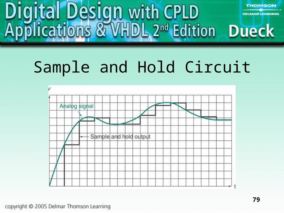
Sample and Hold Circuit
• Required to sample an analog signal at periodic intervals and hold the value long enough for the ADC to convert it to a digital code.
• Generally consists of an input voltage follower, a hold capacitor, and an output voltage follower.

78
Sample and Hold Circuit
79
Sample and Hold Circuit

80
Track and Hold Circuit
• Used in cases where large changes in signal levels between samples are expected.
• Samples the analog signal continuously, minimizing charging delays of the hold capacitor.

81
Sampling Frequency
• A signal must be sampled at a high enough frequency so that no information is lost.
• Aliasing occurs when an unwanted low-frequency component is produced by too slow a sampling frequency.

82
Sampling Frequency

83
Nyquist Sampling Theorem
• To preserve all information in a signal, the signal must be sampled at a rate of twice the highest-frequency component of the signal .maxs f2 f

84
Sampling Frequency Examples
• Since the range of human hearing is 20 Hz to 20 kHz, the sampling frequency for compact disks is set at 44.1 kHz.
• Since the classic telephone bandwidth is 300 Hz to 3300 Hz, telephone-quality signals are sampled at 8 kHz.

85
Filtering• An anti-aliasing filter is used to remove
unwanted high frequency components.
• The filter is a low-pass filter with the corner frequency set to 2fs.

86
Filtering

87
ADC0808 IC ADC – 1
• Successive approximation ADC.
• Able to convert analog information from up to 8 (multiplexed) channels.
• Can form the basis of a data acquisition network.

88
ADC0808 IC ADC – 2
• START conversion with HIGH pulse.• Conversion process driven by the clock. • End-of-conversion indicated by a HIGH on
EOC.• Making OE HIGH allows the digital output to
be read.• When OE inactive, outputs in Hi-Z state.

89
ADC0808 IC ADC – 3

90
ADC0808 IC ADC – 4
Related Documents