c Copyright 2020 Ali Najafi

Welcome message from author
This document is posted to help you gain knowledge. Please leave a comment to let me know what you think about it! Share it to your friends and learn new things together.
Transcript

c©Copyright 2020
Ali Najafi

Low Power Wireless Protocols and Platforms for Internet of Things
Ali Najafi
A dissertationsubmitted in partial fulfillment of the
requirements for the degree of
Doctor of Philosophy
University of Washington
2020
Reading Committee:
Shyam Gollakota, Chair
Joshua Smith
Arvind Krishnamurthy
Program Authorized to Offer Degree:Electrical Engineering

University of Washington
Abstract
Low Power Wireless Protocols and Platforms for Internet of Things
Ali Najafi
Chair of the Supervisory Committee:Associate Professor Shyam Gollakota
Paul G. Allen School of Computer Science & Engineering
Internet of Things (IoT) is an exciting area of research where our goal is to embed connectivity
into billions of everyday objects. There are two key problems to reach this goal. First, existing
wireless communication technologies fail to fulfill the IoT connectivity requirements – low power,
long range, low cost and supporting large number of end points. Backscatter communication is low
power and low cost however it is known to have a limited range. Active radio systems are able to
support long ranges but are power consuming and cost several dollars. Second, the research com-
munity is severely constrained by the lack of a flexible, easily deployable platform for prototyping
IoT endpoints that would allow for ground up protocol development and investigation of how such
protocols perform at scale. In this dissertation, we present wireless communication protocols and
platforms that address these challenges.
We design and build three wireless solutions. We first build LoRa Backscatter, the first wireless
system that provides reliable and long-range communication at tens of microwatts of power as
well as cost less than a dime. Next, we build NetScatter, the first wireless protocol that scales to
hundreds of concurrent transmissions from backscatter devices while being ultra-low power, low
cost and supporting long range. Finally, we build TinySDR, the first SDR platform tailored for IoT
applications which is fully programmable and standalone, consumes ultra-low power during sleep

and supports over the air programming for both physical and MAC layer.
TABLE OF CONTENTS
Page
List of Figures . . . . . . . . . . . . . . . . . . . . . . . . . . . . . . . . . . . . . . . . . . iii
Chapter 1: Introduction . . . . . . . . . . . . . . . . . . . . . . . . . . . . . . . . . . . 11.1 Low-Power Wireless protocols for IoT Networks . . . . . . . . . . . . . . . . . . 11.2 Low-Power SDR Platform for Over-the-Air Programmable IoT Testbeds . . . . . . 81.3 Organization . . . . . . . . . . . . . . . . . . . . . . . . . . . . . . . . . . . . . . 9
Chapter 2: LoRa Backscatter: Enabling The Vision of Ubiquitous Connectivity . . . . . 112.1 The case for LoRa backscatter and Related Work . . . . . . . . . . . . . . . . . . 152.2 System Design . . . . . . . . . . . . . . . . . . . . . . . . . . . . . . . . . . . . 182.3 Hardware Implementation . . . . . . . . . . . . . . . . . . . . . . . . . . . . . . 312.4 Evaluation . . . . . . . . . . . . . . . . . . . . . . . . . . . . . . . . . . . . . . . 342.5 Application Deployments . . . . . . . . . . . . . . . . . . . . . . . . . . . . . . . 41
Chapter 3: NetScatter: Enabling Large-Scale Backscatter Networks . . . . . . . . . . . 493.1 CSS Primer & Existing Approaches . . . . . . . . . . . . . . . . . . . . . . . . . 533.2 NetScatter Design . . . . . . . . . . . . . . . . . . . . . . . . . . . . . . . . . . . 573.3 Addressing Practical Issues . . . . . . . . . . . . . . . . . . . . . . . . . . . . . . 603.4 NetScatter Protocol & Receiver Details . . . . . . . . . . . . . . . . . . . . . . . 673.5 Evaluation . . . . . . . . . . . . . . . . . . . . . . . . . . . . . . . . . . . . . . . 713.6 Related Work . . . . . . . . . . . . . . . . . . . . . . . . . . . . . . . . . . . . . 803.7 Conclusion . . . . . . . . . . . . . . . . . . . . . . . . . . . . . . . . . . . . . . 82
Chapter 4: TinySDR: Low-Power SDR Platform for Over-the-Air Programmable IoTTestbeds . . . . . . . . . . . . . . . . . . . . . . . . . . . . . . . . . . . . . 83
4.1 SDR Requirements for IoT Nodes . . . . . . . . . . . . . . . . . . . . . . . . . . 874.2 TinySDR Platform . . . . . . . . . . . . . . . . . . . . . . . . . . . . . . . . . . 89
i
4.3 Interfacing Between Blocks . . . . . . . . . . . . . . . . . . . . . . . . . . . . . . 944.4 Power Management Unit . . . . . . . . . . . . . . . . . . . . . . . . . . . . . . . 974.5 Over-the-Air Programming protocol . . . . . . . . . . . . . . . . . . . . . . . . . 984.6 TinySDR’s Architectural Considerations . . . . . . . . . . . . . . . . . . . . . . . 1014.7 Case Studies: LoRa and BLE Beacons . . . . . . . . . . . . . . . . . . . . . . . . 1024.8 Evaluation . . . . . . . . . . . . . . . . . . . . . . . . . . . . . . . . . . . . . . . 1064.9 Research Study: Concurrent Reception . . . . . . . . . . . . . . . . . . . . . . . . 1144.10 Conclusion and Research Opportunities . . . . . . . . . . . . . . . . . . . . . . . 116
Chapter 5: Conclusion . . . . . . . . . . . . . . . . . . . . . . . . . . . . . . . . . . . 1195.1 Looking Forward . . . . . . . . . . . . . . . . . . . . . . . . . . . . . . . . . . . 120
Bibliography . . . . . . . . . . . . . . . . . . . . . . . . . . . . . . . . . . . . . . . . . . 121
ii

LIST OF FIGURES
Figure Number Page
1.1 Active and backscatter communication systems. We show different modules inthe two types of communication system technologies. . . . . . . . . . . . . . . . . 2
1.2 Operating distance of backscatter devices. . . . . . . . . . . . . . . . . . . . . . . 4
2.1 LoRa backscatter deployment. The LoRa Backscatter device consumes 9.25 µW,operates at 100s of meters and can be powered by flexible printed batteries and but-ton cells (10 cents), a capability that cannot be achieved with radios. The RF sourcetransmits a single tone that the backscatter device uses to synthesize CSS signals.The challenge is that at the receiver, the backscatter signal is not only drowned bynoise but also suffers interference from the RF source. . . . . . . . . . . . . . . . 12
2.2 We compare power consumption and cost of different communication technologiesincluding backscatter and radio techniques. . . . . . . . . . . . . . . . . . . . . . 14
2.3 CSS modulation & Receiver FFT processing. The two figures on the left showstwo chirp symbols, where the second symbol is a cyclic shifted version of the first,offset by half the chirp duration. BW and SF are the bandwidth and spreadingfactor respectively. The time delays in the chirp translate to a peak in the FFTdomain. The two plots on the right show the FFT output corresponding to the twosymbols. . . . . . . . . . . . . . . . . . . . . . . . . . . . . . . . . . . . . . . . . 19
2.4 Hybrid analog-digital backscatter. The digital baseband processor generates thefrequency plan that is converted in the analog domain to control the output fre-quency of a VCO. The time shifted versions of the VCO output are mapped ac-cording to the dataset of the approximated exponential signal to their respectivebackscatter impedance values using a SP8T RF switch. . . . . . . . . . . . . . . . 21
2.5 Four CSS symbols when spreading factor is 2. . . . . . . . . . . . . . . . . . . . . 222.6 Approximation of a cosine wave with multi-level signal. We approximate the
cosine wave as a sum of three digital signals S0 (t), S1 (t) and S2 (t) resulting in amulti-level signal. . . . . . . . . . . . . . . . . . . . . . . . . . . . . . . . . . . . 26
2.7 LoRa packet structure. . . . . . . . . . . . . . . . . . . . . . . . . . . . . . . . 292.8 We characterize our receiver by measuring PER as a function of reported RSSI in
presence and absence of out of band interference. . . . . . . . . . . . . . . . . . . 34
iii
2.9 RSSI in Deployment scenario 1. d is the distance between the RF source andreceiver. We move the backscatter device along the line joining them. This figurealso shows the corresponding LoRa bit rate at which we successfully receive allour ten packets from the backscatter device without any loss. . . . . . . . . . . . . 37
2.10 RSSI in Deployment scenario 2. d1 (d2) is the distance between the backscatterdevice and RF source (receiver). We fix the location of the backscatter device andRF source and move the receiver away from the backscatter device. . . . . . . . . 38
2.11 The plot on the left demonstrates the efficacy of our harmonic cancellation tech-nique. The right plots CDF of RSSI of a LoRa backscatter device in the presenceand absence of another LoRa backscatter device concurrently transmitting in adja-cent band. . . . . . . . . . . . . . . . . . . . . . . . . . . . . . . . . . . . . . . . 39
2.12 Office Deployment. We receive backscattered packets across one floor of an officebuilding with 13,024 f t2 (1210 m2) area. . . . . . . . . . . . . . . . . . . . . . . . 42
2.13 Home Deployment. We receive packets across the 4,800 f t2 (446 m2) housespread across three floors. . . . . . . . . . . . . . . . . . . . . . . . . . . . . . . . 43
2.14 Precision Agriculture. We measure the RSSI of backscattered packets across a one acre farm. . . 44
2.15 Smart Contact Lens and Flexible epidermal patch sensor. We show the RSSIand data rate distribution across an entire 3,328 f t2 (309 m2) atrium. . . . . . . . . 46
3.1 Large-Scale Network Deployment of Backscatter Devices. We deploy 256 backscat-ter devices across a floor of an office building covering multiple rooms. . . . . . . 50
3.2 NetScatter Overview. In traditional CSS systems, a single device uses differentcyclic shifts to convey bits. In distributed CSS coding, each cyclic shift is assignedto a different backscatter device. Each device then uses the presence and absenceof cyclic shift to send ‘1’ and ‘0’ bits. . . . . . . . . . . . . . . . . . . . . . . . . 51
3.3 CSS Primer. We show upchirp and downchirp symbols and FFT results of theirmultiplication. (a) Baseline upchirp symbol, (b) frequency shifted upchirp symboland (c) cyclically shifted upchirp symbol. . . . . . . . . . . . . . . . . . . . . . . 53
3.4 Choir Approach. We evaluate FFT variation of chirp symbols when BW = 500 kHzand SF = 9 for both active LoRa radios and backscatter devices. . . . . . . . . . . 55
3.5 Bandwidth Aggregation. Here we use an aggregate bandwidth of 2BW but eachdevice transmits only using BW. Upchirps with different cyclic shifts shown indifferent colors. Each upchirp is assigned to a device. . . . . . . . . . . . . . . . . 56
3.6 Timing Mismatch. in detecting beginning of a chirp symbol and its translation toFFT bin variation. . . . . . . . . . . . . . . . . . . . . . . . . . . . . . . . . . . . 59
3.7 Power Adjustment for Backscatter. (a) gain normalized to maximum power as afunction of Z0 impedance and (b) switch network to support multiple power levels. 63
iv
3.8 Normalized Power Spectrum. We show power spectrum of an upchirp multipliedby a baseline downchirp in FFT domain. This plot shows the main lobe and sidelobes of a single chirp transmission. We assign devices to high and low powerregions based on their power level. . . . . . . . . . . . . . . . . . . . . . . . . . . 64
3.9 Backscatter Devices SNR Variance. CDF of SNR variance of backscatter devicesin an office environment, when people were walking around, over 30 mins. . . . . . 66
3.10 NetScatter Network Association Process. We show the association process of anincoming NetScatter device (#2) to the network, while there are existing devicesassociated with the network (i.e., device #1). . . . . . . . . . . . . . . . . . . . . . 68
3.11 Structure of AP’s Query Message. . . . . . . . . . . . . . . . . . . . . . . . . . 70
3.12 Near-Far BER Results. We show the effect of the second device’s power onthe first device’s BER vs. SNR for different ratios of the second device’s to firstdevice’s power with power aware cyclic shift assignments. . . . . . . . . . . . . . 71
3.13 Frequency Offset FFT Bin Variation. (a) frequency offset of backscatter devices,and (b) effect of residual time and frequency offset for different configurations. . . 72
3.14 Our Backscatter Devices. They are arranged closely for this picture. They arespread out across more than ten rooms in our deployment. . . . . . . . . . . . . . 73
3.15 Doppler Effect and Power Dynamic Range Evaluation. We evaluate (a) Dopplereffect, and (b) we show power difference between two concurrent transmissionsat different locations of FFT domain. One transmission is fixed and the other issweeping across different chirp symbols. . . . . . . . . . . . . . . . . . . . . . . . 74
3.16 Spectrogram of Backscattered Signal at the Different Power Levels. . . . . . . 75
3.17 Network Physical Rate. We evaluate NetScatter network physical rate and com-pare it with other schemes. . . . . . . . . . . . . . . . . . . . . . . . . . . . . . . 77
3.18 Link-layer Data Rate. We evaluate link-layer data rate for NetScatter and com-pare it with other schemes. . . . . . . . . . . . . . . . . . . . . . . . . . . . . . . 79
3.19 Network Latency. We evaluate the latency of NetScatter and compare it with otherschemes. We define latency as total time for transmitting all the devices’ data. . . . 80
4.1 TinySDR Hardware Platform. It has two antenna ports for running IoT PHY and MAC protocolsat 2.4 GHz and 900 MHz. This image is the actual size of the platform on printed paper. . . . . . 84
4.2 Radio Module Power Consumption for Each Platform. The TX output powerof each radio module is shown on top of it. . . . . . . . . . . . . . . . . . . . . . . 89
v

4.3 TinySDR System Block Diagram. A complete system diagram showing all ofthe components of tinySDR. This includes the software radio consisting of theradio, amplifiers, and FPGA, OTA programmer which uses a LoRa radio and flashmemory to store programs, and a power managment system with the flexibility toturn off power consuming components. Each of these subsystems are controlled insoftware running on the MCU. . . . . . . . . . . . . . . . . . . . . . . . . . . . . 91
4.4 I/Q Word Structure Used by I/Q Radio. . . . . . . . . . . . . . . . . . . . . . . 944.5 LoRa Packet Structure. . . . . . . . . . . . . . . . . . . . . . . . . . . . . . . . 994.6 LoRa Implementation Block Diagrams. . . . . . . . . . . . . . . . . . . . . . . 1004.7 Evaluation Testbed Map. . . . . . . . . . . . . . . . . . . . . . . . . . . . . . . 1044.8 TinySDR Single-Tone Frequency Spectrum. . . . . . . . . . . . . . . . . . . . 1054.9 Single-Tone Transmitter Power Consumption. We show the total power con-
sumption of tinySDR including I/Q radio, FPGA, MCU and regulators at differenttransmitter output power. This is 15-16 times lower power consumption than theUSRP E310 embedded SDR. . . . . . . . . . . . . . . . . . . . . . . . . . . . . . 107
4.10 LoRa Modulator Evaluation. We evaluate our LoRa modulator in comparisonwith Semtech LoRa chip. . . . . . . . . . . . . . . . . . . . . . . . . . . . . . . . 110
4.11 LoRa Demodulator Evaluation. We evaluate our LoRa demodulator by demod-ulating chirp symbols at different RSSI. . . . . . . . . . . . . . . . . . . . . . . . 110
4.12 BLE evaluation. BLE beacons at different power levels. . . . . . . . . . . . . . . 1134.13 BLE Beacons Signal. We show BLE beacon transmissions on three advertising
channels from tinySDR using an envelope detector. . . . . . . . . . . . . . . . . . 1134.14 OTA Programming Time. We show CDF of OTA programming time for pro-
gramming LoRa and BLE implementations on tinySDR. . . . . . . . . . . . . . . 1144.15 Orthogonal LoRa Demodulation Evaluation . . . . . . . . . . . . . . . . . . . 117
vi

ACKNOWLEDGMENTS
First, I would like to truly thank my advisor Professor Shyam Gollakota for all the support,
mentorship and giving me the freedom to work on wide spectrum of problems that excites me.
I also want to thank Professor Visvesh Sathe for teaching me digital circuits and VLSI and help-
ing me during early phase of my PhD. I want to thank Jacob Sunshine for having great discussions.
I want to thank Josh Smith and Tom Anderson for helping me during my job search.
I would like to thank all the current and previous lab members at Networks and Mobile Systems
lab. I specially want to thank Mehrdad Hessar, Vikram Iyer and Justin Chan with whom I had the
pleasure of working, having great discussions and learning a lot. I also want to thank Sensor
Systems Lab members specially Mohammad Katanbaf for great suggestions and feedbacks. In
addition, I want to thank Tong Zhang for teaching me about IC fabrication and testing process.
I want to thank Professor Josh Smith, Arvind Krishnamurthy and Mehran Mesbahi for accept-
ing to participate in my committee.
I also want to thank my managers and mentors at Qualcomm and Apple. Specially, I would
like to thank Mansour Keramat in Apple for working closely with me and teaching me about signal
processing and system design. I want to thank Vahid Majidzadeh in Apple, Rabih Makarem and
Soheil Golara in Qualcomm for being great mentors and collaborators.
Finally, I would like to thank my family and friends. Specially, I can not put in words how
much I am thankful to my parents who have always shown utmost unconditional love and support
throughout my life. I also want to thank my partner, my brother and my sister for being great
support during these years.
vii

DEDICATION
to my parents
viii

1
Chapter 1
INTRODUCTION
Internet of Things (IoT) purpose is to provide wireless connectivity for everyday objects. IoT
has applications in various industries including smart home and smart building, wearables, agricul-
ture and manufacturing. We want to be able to check the room occupancy in the building and set
the air conditioners accordingly to save energy. We have wireless medical sensors like biosensor
stickers to allow patient mobility and enhance their quality of life. In agriculture, we want sensor
nodes to monitor soil humidity or figure out crop quality using cameras and computer vision. All
these applications require wireless connectivity.
IoT wireless connectivity solutions should satisfy four requirements. They should consume low
power so that they can last on a small battery for a long time. This way we can deploy the sensors
and let them run for few years without maintenance. They should support dense networks to fulfill
our goal of connecting billions of everyday objects. They should be able to support long ranges.
Finally, an ideal IoT connectivity solution should be low cost to enable widespread adaptation.
The problem is that existing communication technologies fail to fulfill the IoT connectivity
requirements. Furthermore, the research community is severely constrained by the lack of a flexible
platform which would allow for IoT protocol development and innovation. Before, we go into the
details of these systems, we provide the motivation and high-level description of these systems.
1.1 Low-Power Wireless protocols for IoT Networks
Let’s look at existing wireless communication technologies. Active radio technologies including
Wi-Fi, ZigBee, SigFox [53], LoRa [39] and LTE-M [12] provide reliable coverage and long ranges
2
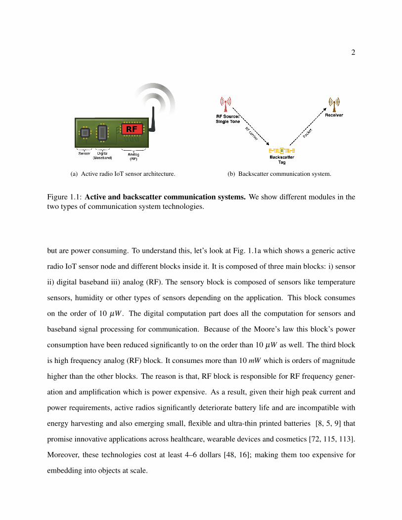
(a) Active radio IoT sensor architecture. (b) Backscatter communication system.
Figure 1.1: Active and backscatter communication systems. We show different modules in thetwo types of communication system technologies.
but are power consuming. To understand this, let’s look at Fig. 1.1a which shows a generic active
radio IoT sensor node and different blocks inside it. It is composed of three main blocks: i) sensor
ii) digital baseband iii) analog (RF). The sensory block is composed of sensors like temperature
sensors, humidity or other types of sensors depending on the application. This block consumes
on the order of 10 µW . The digital computation part does all the computation for sensors and
baseband signal processing for communication. Because of the Moore’s law this block’s power
consumption have been reduced significantly to on the order than 10 µW as well. The third block
is high frequency analog (RF) block. It consumes more than 10 mW which is orders of magnitude
higher than the other blocks. The reason is that, RF block is responsible for RF frequency gener-
ation and amplification which is power expensive. As a result, given their high peak current and
power requirements, active radios significantly deteriorate battery life and are incompatible with
energy harvesting and also emerging small, flexible and ultra-thin printed batteries [8, 5, 9] that
promise innovative applications across healthcare, wearable devices and cosmetics [72, 115, 113].
Moreover, these technologies cost at least 4–6 dollars [48, 16]; making them too expensive for
embedding into objects at scale.

3
As explained, the RF block is the dominant power consumer in active radio sensor nodes and
if we can remove this block we would be able to lower the sensor node’s power consumption by
several orders of magnitude. Backscatter communication is such a solution in which the RF power
generation and amplification is done by another separate module which does not have the power
constraints of the sensor node. Fig.1.1b shows the backscatter communication system. It is com-
posed of an RF power source, backscatter sensor node and an RF receiver. The RF source generates
the single-tone RF carrier and the tag would either reflect or absorb this signal to modulate the data.
The receiver will receive this modulated data. As a result, the backscatter node consumes orders
of magnitude lower power since it is not generating the RF frequency.
Backscatter promises to be an extremely low power, smaller and cheaper alternative to active
radios. Given the absence of expensive radio analog components including RF oscillators, de-
coupling capacitors and crystals, backscatter designs including passive RFID and Wi-Fi backscat-
ter [102, 96] cost only a few cents to manufacture at scale [38]. Further, they consume three to
four orders of magnitude lower power and peak current than radios and hence can operate with
emerging flexible, printed and ultra-thin printed battery technologies. However, despite all these
benefits, current backscatter designs have seen very limited adoption beyond RFID applications.
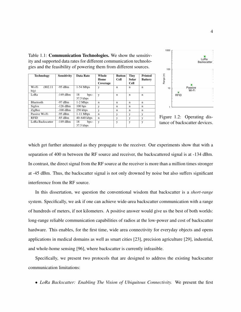
This is because current backscatter designs are unreliable, limited in operating range, and in fact
today cannot achieve robust coverage across rooms [96, 84, 2, 144] as outlined in Fig. 1.2 and Ta-
ble 1.1 1. Furthermore, since RF signals get significantly attenuated by the human body, backscatter
range is limited to tens of centimeters in several healthcare and wearable device applications [96].
To understand this, consider the deployment in Fig. 1.1b. Here the backscatter device reflects
signals from an RF source to synthesize data packets that are then decoded by a receiver. The
challenge is that, before arriving at the backscatter device, the signals from the RF source are
already attenuated. The backscatter device can reflect these weak signals to synthesize data packets
1We note that active RFID does not use backscatter. Instead, it uses radios, is power consuming and costs between15–100 dollars [138, 76].
4
Table 1.1: Communication Technologies. We show the sensitiv-ity and supported data rates for different communication technolo-gies and the feasibility of powering them from different sources.
Technology Sensitivity Data Rate WholeHomeCoverage
ButtonCell
TinySolarCell
PrintedBattery
Wi-Fi (802.11b/g)
-95 dBm 1-54 Mbps y n n n
LoRa -149 dBm 18 bps–37.5 kbps
y n n n
Bluetooth -97 dBm 1-2 Mbps n n n nSigfox -126 dBm 100 bps y n n nZigBee -100 dBm 250 kbps y n n nPassive Wi-Fi -95 dBm 1-11 Mbps n y y yRFID -85 dBm 40–640 kbps n y y yLoRa Backscatter -149 dBm 18 bps–
37.5 kbpsy y y y
1
10
100
1000
Ra
ng
e (
m)
RFID
Passive Wi-Fi
LoRa Backscatter
Figure 1.2: Operating dis-tance of backscatter devices.
which get further attenuated as they propagate to the receiver. Our experiments show that with a
separation of 400 m between the RF source and receiver, the backscattered signal is at -134 dBm.
In contrast, the direct signal from the RF source at the receiver is more than a million times stronger
at -45 dBm. Thus, the backscatter signal is not only drowned by noise but also suffers significant
interference from the RF source.
In this dissertation, we question the conventional wisdom that backscatter is a short-range
system. Specifically, we ask if one can achieve wide-area backscatter communication with a range
of hundreds of meters, if not kilometers. A positive answer would give us the best of both worlds:
long-range reliable communication capabilities of radios at the low-power and cost of backscatter
hardware. This enables, for the first time, wide area connectivity for everyday objects and opens
applications in medical domains as well as smart cities [23], precision agriculture [29], industrial,
and whole-home sensing [96], where backscatter is currently infeasible.
Specifically, we present two protocols that are designed to address the existing backscatter
communication limitations:
• LoRa Backscatter: Enabling The Vision of Ubiquitous Connectivity. We present the first
5
wide-area backscatter system. Our system is the first chirp spread spectrum (CSS) backscat-
ter design. It can successfully backscatter from any location between an RF source and
receiver, separated by 475 m, while being compatible with commodity LoRa hardware. Fur-
ther, when our backscatter device is co-located with the RF source, the receiver can be as far
as 2.8 km away. We deploy our system in a three-floor house, office area and vegetable farm
and show that we can achieve reliable coverage using only a single RF source and receiver.
• NetScatter: Enabling Large-Scale Backscatter Networks. Next, we explore how can we
support a large number of backscatter devices in a wide area? We present the first wireless
protocol that scales to hundreds of concurrent transmissions from backscatter devices. Our
key innovation is a distributed coding mechanism that works below the noise floor, operates
on backscatter devices and can decode all the concurrent transmissions at the receiver using
a single FFT operation. Our design addresses practical issues such as timing and frequency
synchronization as well as the near-far problem. We deploy our design using a testbed of
backscatter hardware and show that our protocol scales to concurrent transmissions from
256 devices using a bandwidth of only 500 kHz.
1.1.1 LoRa Backscatter: Enabling The Vision of Ubiquitous Connectivity [141]
LoRa Backscatter, the subject of Chapter 2, presents a wireless communication solution that is
long-range, ultra-low-power and low-cost. Existing communication technologies cannot satisfy
these requirements at the same time. Backscatter communication is low power and low cost how-
ever it is known to have a limited range. Active radio systems are able to support long ranges but
are power consuming and cost several dollars. To overcome this, we designed LoRa Backscatter
which is the first communication technology that provides reliable and long-range communication
at tens of microwatts of power as well as cost less than a dime.
To design this system, we first profile existing radio technologies in Table. 1.1, which shows

6
that LoRa provides the highest sensitivity of -149 dBm and supports bit rates of 18 bps to 37.5 kbps,
which are sufficient for most IoT applications. Further, LoRa is resilient to both in-band and out-of-
band interference [43]. Specifically, the Sx1276 receiver hardware from SEMTECH can reliably
decode LoRa packets in the presence of 95 dB higher out of band interference [43]. This is signif-
icant because as described above, in typical backscatter deployments, the backscattered signal at
the receiver can be as low as -135 dBm and this signal must be decoded in the presence of a strong
single tone out of band interference as high as -45 dBm. 95 dB out of band interference specifi-
cations of Sx1276 Lora receivers by SEMTECH satisfy these stringent requirements. Motivated
by this, we present the design and implementation of the first LoRa backscatter system. At a high
level, the RF source transmits a single tone signal, which our backscatter devices use to synthesize
LoRa compatible packets. The details of this system are explained in Chapter 2. Our design can
successfully backscatter from any location between an RF source and receiver, separated by 475 m,
while being compatible with commodity LoRa hardware. Further, when our backscatter device is
co-located with the RF source, the receiver can be as far as 2.8 km away. We deploy our system in
a 4,800 f t2 (446 m2) house spread across three floors, a 13,024 f t2 (1210 m2) office area covering
41 rooms, as well as a one-acre (4046 m2) vegetable farm and show that we can achieve reliable
coverage, using only a single RF source and receiver. We also build a contact lens prototype as
well as a flexible epidermal patch device attached to the human skin. We show that these devices
can reliably backscatter data across a 3,328 ft2 (309 m2) room. Finally, we present a design sketch
of a LoRa backscatter IC that shows that it costs less than a dime at scale and consumes only 9.25
µW of power, which is more than 1000x lower power than LoRa radio chipsets.
1.1.2 NetScatter: Enabling Large-Scale Backscatter Networks [89]
In the previous chapter, we talked about how we can extend the range of backscatter communica-
tion to several hundred meters. Our goal in this chapter is to design a network protocol that enables

7
these low-power backscatter networks to support hundreds to thousands of concurrent transmis-
sions. This is challenging because the resulting design must operate reliably with weak backscatter
signals that can be close to or below the noise floor. To this end, we present NetScatter, the
first wireless protocol that can scale to hundreds and thousands of concurrent transmissions from
backscatter devices. Our key innovation is a distributed coding mechanism that satisfies four key
constraints: i) it enables hundreds of devices to concurrently transmit on the same frequency band,
ii) it can operate below the noise floor while achieving reasonable bitrates, iii) its coding operation
can be performed by low-power backscatter devices, and iv) it can decode all the transmissions at
the receiver using a single FFT operation, thus minimizing the receiver complexity.
We introduce distributed chirp spread spectrum coding, which uses a combination of chirp
spread spectrum (CSS) modulation and ON-OFF keying. In existing CSS systems (e.g., LoRa
backscatter [141]), the AP transmits a continuous wave signal which each device backscatters
and encodes bits using different cyclic shifts of a chirp signal. In contrast, in our distributed CSS
coding, we assign a different cyclic shift of the chirp to each of the concurrent devices. Each device
uses ON-OFF keying over these cyclic shifted chirps to convey bits, i.e., the presence and absence
of the corresponding cyclic shifted chirp correspond to a ‘1’ and ‘0’ bit respectively. Note that in
comparison to existing CSS systems where each device transmits log2N bits using N cyclic shifts,
our distributed design enables N concurrent devices, each of which transmits a single bit, using
ON-OFF keying. Thus, our design transmits a total of N bits within a chirp duration, providing a
theoretical gain of Nlog2N .
Our design leverages the fact that creating concurrent cyclic-shifted chirps at a single device
requires distributing its transmit power amongst all the cyclic shifts, which reduces the ability of
the receiver to decode each chirp. Instead we generate concurrent cyclic-shifted chirps across a
distributed set of low-power devices in the network. This allows us to efficiently leverage the
coding gain provided by chirp spread spectrum under the noise floor [71]. Further, we can decode
8
all the concurrent transmissions using a single FFT operation, since cyclic shifting the chirps in the
time domain translates to offsets in the frequency domain.
We implement NetScatter on a testbed of backscatter devices. We create backscatter hardware
that implements NetScatter and includes circuits to perform automatic power adaptation before
each transmission. We deploy our backscatter testbed with 256 devices in an office building span-
ning multiple rooms. We implement our receiver algorithm using USRP X-300 software-defined
radios. Our results reveal that over a 256 node backscatter deployment, NetScatter achieves a 14–
62x gain over prior long-range backscatter systems [141] for its end-to-end link layer data rates.
The key benefit however is in the network latency which sees a reduction of 15–67x.
1.2 Low-Power SDR Platform for Over-the-Air Programmable IoT Testbeds
Motivated by the challenges of building the network in NetScatter, next we were motivated to build
a platform so others do not have to reinvent the wheel. In fact, today, the research community is
handicapped by the lack of a flexible, easily deployable platform for prototyping IoT endpoints
that would allow for ground up protocol development and investigation of how such protocols
perform at scale. We built tinySDR, the first software-defined radio platform tailored to the needs
of power-constrained IoT endpoints. TinySDR provides a standalone, fully programmable low
power software-defined radio solution that can be duty cycled for battery operation like a real
IoT endpoint, and more importantly, can be programmed over the air to allow for large scale
deployment. We present extensive evaluation of our platform showing it consumes as little as 30
µW of power in sleep mode, which is 10,000x lower than existing SDR platforms.
Designing such an SDR platform required addressing multiple systems, architecture, power
and engineering challenges:
• Low-power hardware architecture. Achieving a small form-factor, low-power SDR re-
quires a minimalist design approach that can satisfy the real-time needs of IoT protocols and
9
ensure flexibility at the PHY and MAC layers. To do this, we exploit recent advances in
small, low-power microcontrollers, FPGAs and flash memory to pick the right components
for our platform. We use a low-power FPGA to run the PHY layer while the microcontroller
runs the MAC protocols as well as handles the I/O operations between the FPGA, radio,
memory and sensor interfaces.
• Efficient power management. Achieving highly granular power management needed for
battery-powered operation and enabling ultra-low power sleep modes requires shutting down
parts of SDR when not in use. This is important for IoT endpoints that perform duty-cycled
operations and require an ultra-low power sleep mode to achieve a long battery life. This
presents a design tradeoff between the complexity of toggling the power of each hardware
component ON and OFF, and the cost of additional circuitry to do so.
• Over-the-air SDR programming. Enabling a truly scalable system requires the ability to
update the PHY and MAC layers on the platform, over-the-air, in a testbed deployment.
This however also introduces the challenge of over-the-air FPGA and microcontroller pro-
gramming as well as communicating these updates robustly to each device in the network
while minimizing power consumption and network utilization. We use a dedicated wireless
backbone subsystem complete with a MAC protocol and its own flash memory to program
both the microcontroller and FPGA. Additionally we leverage compression and low-power
decompression algorithms to minimize network downtime during the updates.
1.3 Organization
The rest of this dissertation is organized as follows. In Chapter 2, we describe LoRa Backscatter in
more details, go over system design, how we were able to synthesize Chirp Spread Spectrum (CSS)
in a low power tag as well as link-layer protocol and evaluation in several deployment scenarios.
10
Chapter 3 describes how we modified CSS to build our Distributed CSS (DCSS) in NetScatter and
achieve concurrent transmissions from several hundreds backscatter tags. Moreover, we show how
NetScatter is addressing the challenges of timing synchronization and near-far. Chapter 4 presents
TinySDR and describes how we were able to achieve low power consumption and add over the air
update functionality in an Software-Defined Radio. Finally, Chapter 5 concludes the dissertation
with thoughts for the future direction for this line of work.
11
Chapter 2
LORA BACKSCATTER: ENABLING THE VISION OF UBIQUITOUSCONNECTIVITY
Embedding cheap, reliable and low power connectivity into medical sensors is challenging.
Active radio technologies including Wi-Fi, ZigBee, SigFox [53], LoRa [39] and LTE-M [12] pro-
vide reliable coverage and long ranges but consume between 10 to 500 mW [44, 47, 46, 98, 162]
and cost at least 4–6 dollars [48, 16]; making them too expensive for embedding into medical
sensors. Further, given their high peak current and power requirements, active radios significantly
deteriorate battery life and are incompatible with emerging small, flexible and ultra-thin printed
batteries [8, 5, 9] that promise innovative applications across healthcare, wearable devices and
cosmetics [72, 115, 113].
Backscatter promises to be an extremely low power, smaller and cheaper alternative to active
radios. Given the absence of expensive radio analog components including RF oscillators, de-
coupling capacitors and crystals, backscatter designs including passive RFID and Wi-Fi backscat-
ter [102, 96] cost only a few cents to manufacture at scale [38]. Further, they consume three to four
orders of magnitude lower power and peak current than radios and hence can operate with emerg-
ing flexible, printed and ultra-thin printed battery technologies. However, despite all these benefits,
current backscatter designs have seen very limited adoption beyond RFID applications. This is
because current backscatter designs are unreliable, limited in operating range, and in fact today
cannot achieve robust coverage across rooms [96, 84, 2, 144] as outlined in Fig. 1.2 and Table 1.1 1
. Furthermore, since RF signals get significantly attenuated by the human body, backscatter range
1We note that active RFID does not use backscatter. Instead, it uses radios, is power consuming and costs between15–100 dollars [138, 76].

12
Figure 2.1: LoRa backscatter deployment. The LoRa Backscatter device consumes 9.25 µW,operates at 100s of meters and can be powered by flexible printed batteries and button cells (10cents), a capability that cannot be achieved with radios. The RF source transmits a single tone thatthe backscatter device uses to synthesize CSS signals. The challenge is that at the receiver, thebackscatter signal is not only drowned by noise but also suffers interference from the RF source.
is limited to tens of centimeters in several healthcare and wearable device applications [96].
In this chapter, we question the conventional wisdom that backscatter is a short-range sys-
tem. Specifically, we ask if one can achieve wide-area backscatter communication with a range of
hundreds of meters, if not kilometers. A positive answer would give us the best of both worlds:
long-range reliable communication capabilities of radios at the low-power and cost of backscatter
hardware. This enables, for the first time, wide area connectivity for everyday objects and opens
applications in medical domains as well as smart cities [23], precision agriculture [29], industrial,
and whole-home sensing [96], where backscatter is currently infeasible.
To appreciate why this is hard, consider the deployment in Fig. 2.1. Here the backscatter device
reflects signals from an RF source to synthesize data packets that are then decoded by a receiver.
The challenge is that, before arriving at the backscatter device, the signals from the RF source are
already attenuated. The backscatter device can reflect these weak signals to synthesize data packets
which get further attenuated as they propagate to the receiver. Our experiments show that with a
separation of 400 m between the RF source and receiver, the backscattered signal is at -134 dBm.
In contrast, the direct signal from the RF source at the receiver is more than a million times stronger
at -45 dBm. Thus, the backscatter signal is not only drowned by noise but also suffers significant
interference from the RF source.
13
We present the first wide-area backscatter communication system. Achieving this requires us
to satisfy two key constraints. First, the backscatter device should code information in a way
that can be decoded at the receiver down to and below -135 dBm signal strength and reliably
operate in the presence of strong out-of-band interference. Second, instead of using a custom
receiver for the backscattered signal that can be prohibitively expensive (e.g., RFID readers), the
backscattered signals should be decoded on readily and cheaply available commodity hardware
that would expedite the adoption and development of our design.
To do so, we first profile existing radio technologies in Table. 1.1, which shows that LoRa
provides the highest sensitivity of -149 dBm and supports bit rates of 18 bps to 37.5 kbps, which
are sufficient for most IoT applications. Further, LoRa is resilient to both in-band and out-of-band
interference [43]. Specifically, the Sx1276 receiver hardware from SEMTECH can reliably decode
LoRa packets in the presence of 95 dB higher out of band interference [43]. This is significant
because as described above, in typical backscatter deployments, the backscattered signal at the re-
ceiver can be as low as -135 dBm and this signal must be decoded in the presence of a strong single
tone out of band interference as high as -45 dBm. 95 dB out of band interference specifications
of Sx1276 Lora receivers by SEMTECH satisfy these stringent requirements. Motivated by this,
we present the design and implementation of the first LoRa backscatter system. At a high level,
the RF source transmits a single tone signal, which our backscatter devices use to synthesize LoRa
compatible packets. To achieve this, we make two key technical contributions.
• We introduce the first chirp spread spectrum (CSS) backscatter design. LoRa uses CSS
modulation where, as shown in Fig. 2.3a, a ‘0’ bit can be represented as a continuous chirp
that increases linearly with frequency, while a ‘1’ bit is a chirp that is cyclically shifted
in time. Thus, CSS requires continuously changing the frequency as a function of time,
which has not been demonstrated on backscatter hardware. This is challenging since while
existing backscatter approaches can generate DBPSK/DQPSK (802.11b/ZigBee [102, 96])
14
0.1
1
10
100
1000
10000
100000
1e+06
Pow
er
Consum
ption (
uW
)
Backscatter
Active Radio
RFIDLoRa
Backscatter
Passive Wi-Fi
ZigBee
SigFox
Bluetooth
LoRa
Wi-Fi
(a) Power consumption
0
1
2
3
4
5
6
7
8
Cost ($
)
Backscatter
Active Radio
LoRa Backscatter
Passive Wi-Fi
RFID
Bluetooth
SigFox ZigBee
LoRa
Wi-Fi
(b) Cost of communication
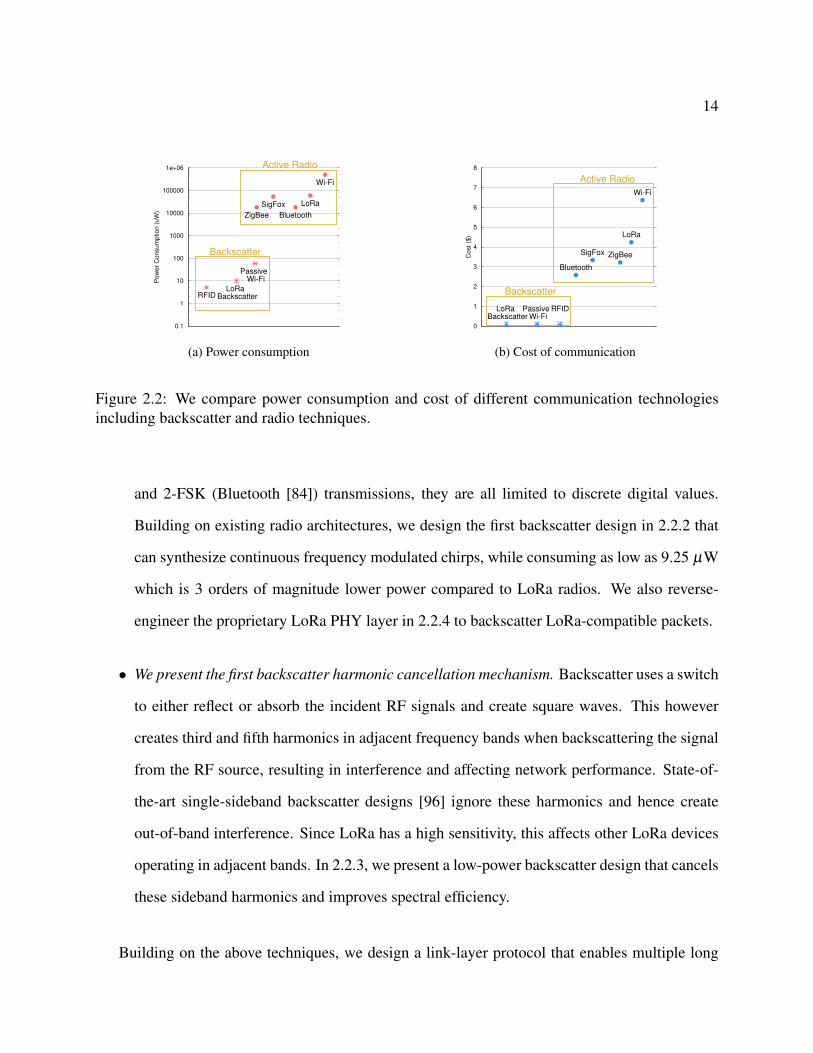
Figure 2.2: We compare power consumption and cost of different communication technologiesincluding backscatter and radio techniques.
and 2-FSK (Bluetooth [84]) transmissions, they are all limited to discrete digital values.
Building on existing radio architectures, we design the first backscatter design in 2.2.2 that
can synthesize continuous frequency modulated chirps, while consuming as low as 9.25 µW
which is 3 orders of magnitude lower power compared to LoRa radios. We also reverse-
engineer the proprietary LoRa PHY layer in 2.2.4 to backscatter LoRa-compatible packets.
• We present the first backscatter harmonic cancellation mechanism. Backscatter uses a switch
to either reflect or absorb the incident RF signals and create square waves. This however
creates third and fifth harmonics in adjacent frequency bands when backscattering the signal
from the RF source, resulting in interference and affecting network performance. State-of-
the-art single-sideband backscatter designs [96] ignore these harmonics and hence create
out-of-band interference. Since LoRa has a high sensitivity, this affects other LoRa devices
operating in adjacent bands. In 2.2.3, we present a low-power backscatter design that cancels
these sideband harmonics and improves spectral efficiency.
Building on the above techniques, we design a link-layer protocol that enables multiple long

15
range backscatter devices to share the spectrum. We also design a LoRa backscatter IC and estimate
the power consumption using Cadence and Synopsis software toolkits [6, 15]. Our results show that
our IC design is comparable in area to RFID and consumes as little as 9.25 µW while generating
continuous frequency modulated chirps and performing harmonic cancellation.
Below, we summarize our evaluation in various deployment scenarios:
• We evaluate our design in various line-of-sight scenarios. Our results show that even when
the RF source and receiver are separated by 475 m, the backscatter device could operate
at all locations between them. Further, when the backscatter device is co-located with the
RF source, the LoRa receiver can decode transmissions from as far as 2.8 km from the
backscatter device.
• Finally, we show that our design can also enable backscatter in applications that are not
favorable for RF propagation. Specifically, we evaluate a contact lens form factor antenna
in-vitro and show that it can easily backscatter data from across a 3,328 f t2 (309 m2) room
using only a single RF source and receiver. This is orders of magnitude larger than the
35 inch (89 cm) range achieved by prior designs [96]. We also build a flexible epidermal
patch sensor that backscatters data in the above room, while being attached to human skin.
2.1 The case for LoRa backscatter and Related Work
To demonstrate that LoRa backscatter is the best fit for achieving ubiquitous connectivity, we first
compare it with existing solutions and show how it fares across the spectrum of power consump-
tion, cost, size, sources of power and operating range. We then discuss prior work and compare
our LoRa backscatter system with state of the art backscatter approaches.
• Operating range. Fig. 1.2 shows the range of different radio and backscatter communication
solutions. Radios including Wi-Fi, Bluetooth and ZigBee operate up to 100s of meters while

16
wide area LoRa and SigFox deployments extend operation to kilometers. However, existing
backscatter solutions such as RFID and Passive Wi-Fi are limited to tens of meters of operat-
ing distance in best-case scenarios. LoRa backscatter instead extends backscatter operation
to 100s of meters. This achieves the whole home and office coverage of Wi-Fi and ZigBee
radios while delivering the cost, size and power benefits of backscatter described below.
• Power consumption. Fig. 2.2a shows the power consumption of popular radio and exist-
ing backscatter solutions. Radios including Wi-Fi, BLE, ZigBee, Lora and SigFox all con-
sume between 10 to 500 mW [44, 47, 46, 79, 161, 80], which is 3–4 orders of magnitude
higher than the power consumption of backscatter systems including RFID, Passive Wi-Fi
and the LoRa backscatter system. LoRa backscatter consumes three orders of magnitude
lower power than LoRa radios and would significantly extend the battery life. Further it can
easily operate for more than 10 years on button cells and printed batteries that are fraction of
the size of batteries used with LoRa radios.
• Cost and size. Fig. 2.2b plots the cost of active radio and backscatter communication so-
lutions. Radios are at least an order of magnitude more expensive compared to backscatter
solutions. This is because an active radio requires analog RF components such as local os-
cillators, mixers and amplifiers that consume significant silicon area. Since, the cost of an
IC is directly proportional to silicon area, the analog components increase the cost of radios.
Additionally, radios require external components such as crystals, matching inductors and
decoupling capacitors all of which increase the overall cost. In contrast, backscatter solu-
tions are primarily digital in nature and scale with Moore’s law that significantly reduce the
area and consequently the cost of the backscatter IC to few cents. Also, backscatter com-
munication modules can be built with just an IC, printed antenna and tiny battery and do
not require external components like crystals, inductors and decoupling capacitors which
17
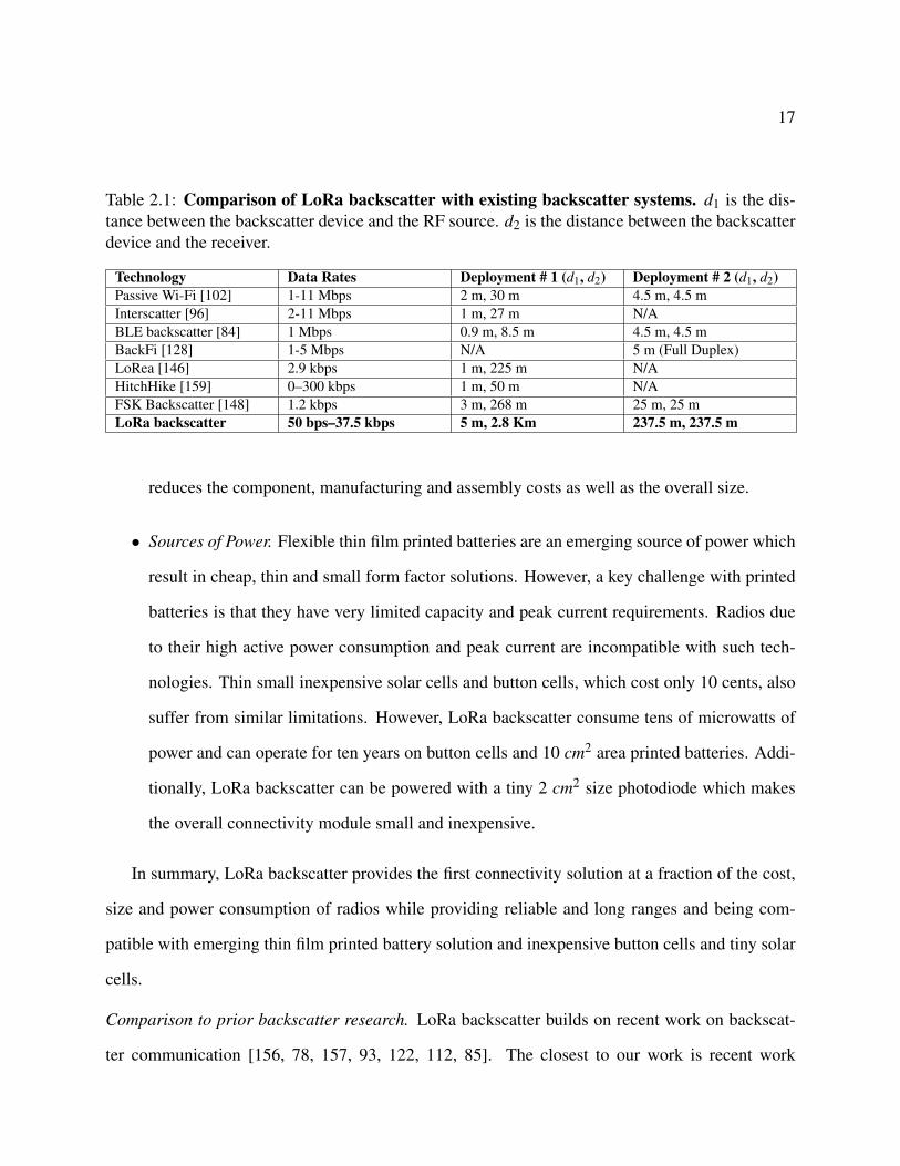
Table 2.1: Comparison of LoRa backscatter with existing backscatter systems. d1 is the dis-tance between the backscatter device and the RF source. d2 is the distance between the backscatterdevice and the receiver.
Technology Data Rates Deployment # 1 (d1, d2) Deployment # 2 (d1, d2)Passive Wi-Fi [102] 1-11 Mbps 2 m, 30 m 4.5 m, 4.5 mInterscatter [96] 2-11 Mbps 1 m, 27 m N/ABLE backscatter [84] 1 Mbps 0.9 m, 8.5 m 4.5 m, 4.5 mBackFi [128] 1-5 Mbps N/A 5 m (Full Duplex)LoRea [146] 2.9 kbps 1 m, 225 m N/AHitchHike [159] 0–300 kbps 1 m, 50 m N/AFSK Backscatter [148] 1.2 kbps 3 m, 268 m 25 m, 25 mLoRa backscatter 50 bps–37.5 kbps 5 m, 2.8 Km 237.5 m, 237.5 m
reduces the component, manufacturing and assembly costs as well as the overall size.
• Sources of Power. Flexible thin film printed batteries are an emerging source of power which
result in cheap, thin and small form factor solutions. However, a key challenge with printed
batteries is that they have very limited capacity and peak current requirements. Radios due
to their high active power consumption and peak current are incompatible with such tech-
nologies. Thin small inexpensive solar cells and button cells, which cost only 10 cents, also
suffer from similar limitations. However, LoRa backscatter consume tens of microwatts of
power and can operate for ten years on button cells and 10 cm2 area printed batteries. Addi-
tionally, LoRa backscatter can be powered with a tiny 2 cm2 size photodiode which makes
the overall connectivity module small and inexpensive.
In summary, LoRa backscatter provides the first connectivity solution at a fraction of the cost,
size and power consumption of radios while providing reliable and long ranges and being com-
patible with emerging thin film printed battery solution and inexpensive button cells and tiny solar
cells.
Comparison to prior backscatter research. LoRa backscatter builds on recent work on backscat-
ter communication [156, 78, 157, 93, 122, 112, 85]. The closest to our work is recent work

18
that backscatters ambient signals like TV [111, 125], Wi-Fi [101, 128, 102, 160, 159], Blue-
tooth [84, 160, 127] and ZigBee [127, 96]. A comparison of the LoRa backscatter system with
existing backscatter systems in terms of data rates and ranges is shown in Table 2.1. In the table,
deployment # 1 refers to the scenario where the backscatter device is placed near the signal source
(d1) and the receiver is placed at a distant location (d2). In deployment #2, the backscatter device
is equidistant to the signal source and receiver (d1 = d2) and demonstrates the practical operating
range of backscatter systems.
As seen from Table 2.1, existing backscatter systems have a range of 10 m, when the backscatter
device is 6 m away from the RF source and 50 m when the backscatter device is 1 m away [159].
[148, 146] uses FSK modulation to increase the backscatter range. Specifically, the authors show
that when the backscatter tag is 3 m from the RF source, the receiver can be 246 m away. In
more realistic scenarios, when the tag is around 25 m from the signal source and the receiver, their
packet error rate was 100%. In a similar setup, we can deliver packets even when the receiver
is 2.8 km away. Our design uses CSS modulation and achieves much higher sensitivities. As a
result, we achieve 1–2 orders of magnitude higher communication ranges and thus enable wide-
area backscatter.
2.2 System Design
LoRa backscatter uses chirp spread spectrum (CSS) to design a wide-area backscatter communi-
cation system. In this section, we first provide an overview of CSS. We then present our hybrid
analog-digital backscatter design to create CSS transmissions as well as our harmonic cancellation
mechanism. We then describe how to synthesize CSS packets that are compatible with the LoRa
physical layer by reverse-engineering LoRa. Finally, we outline a link-layer protocol that enables
multiple CSS backscatter devices to co-exist with each other.
19
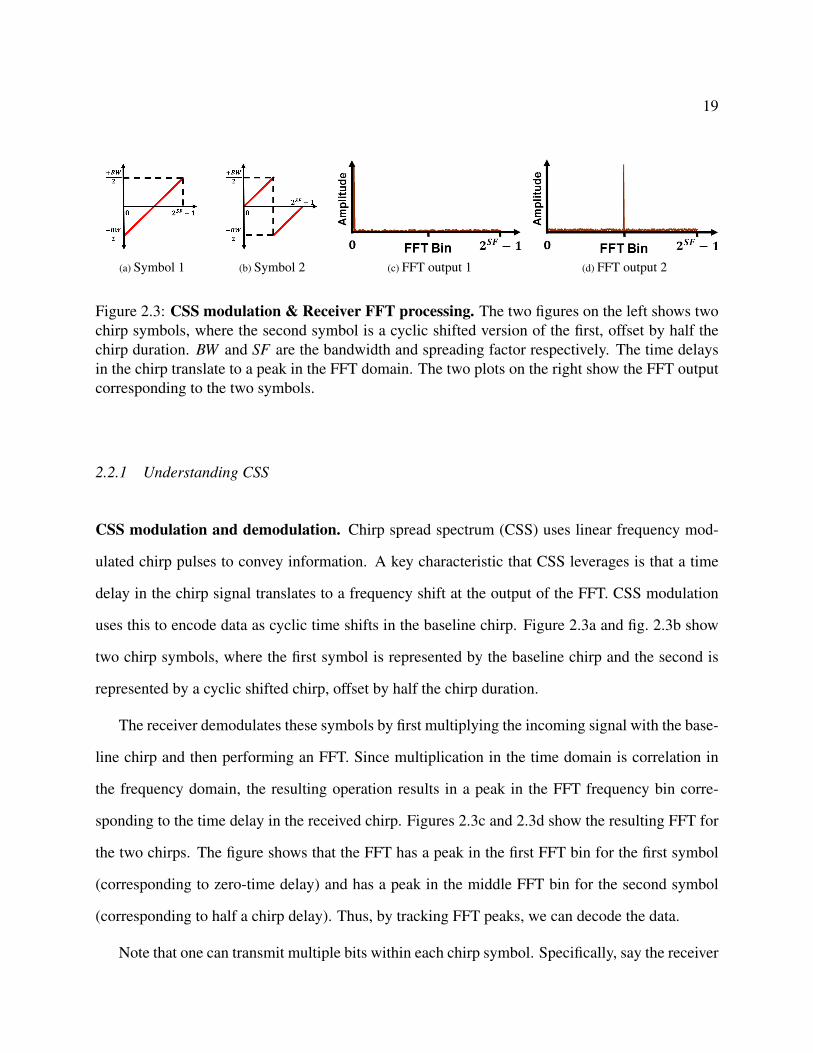
(a) Symbol 1 (b) Symbol 2 (c) FFT output 1 (d) FFT output 2
Figure 2.3: CSS modulation & Receiver FFT processing. The two figures on the left shows twochirp symbols, where the second symbol is a cyclic shifted version of the first, offset by half thechirp duration. BW and SF are the bandwidth and spreading factor respectively. The time delaysin the chirp translate to a peak in the FFT domain. The two plots on the right show the FFT outputcorresponding to the two symbols.
2.2.1 Understanding CSS
CSS modulation and demodulation. Chirp spread spectrum (CSS) uses linear frequency mod-
ulated chirp pulses to convey information. A key characteristic that CSS leverages is that a time
delay in the chirp signal translates to a frequency shift at the output of the FFT. CSS modulation
uses this to encode data as cyclic time shifts in the baseline chirp. Figure 2.3a and fig. 2.3b show
two chirp symbols, where the first symbol is represented by the baseline chirp and the second is
represented by a cyclic shifted chirp, offset by half the chirp duration.
The receiver demodulates these symbols by first multiplying the incoming signal with the base-
line chirp and then performing an FFT. Since multiplication in the time domain is correlation in
the frequency domain, the resulting operation results in a peak in the FFT frequency bin corre-
sponding to the time delay in the received chirp. Figures 2.3c and 2.3d show the resulting FFT for
the two chirps. The figure shows that the FFT has a peak in the first FFT bin for the first symbol
(corresponding to zero-time delay) and has a peak in the middle FFT bin for the second symbol
(corresponding to half a chirp delay). Thus, by tracking FFT peaks, we can decode the data.
Note that one can transmit multiple bits within each chirp symbol. Specifically, say the receiver
20
performs a N point FFT. It can distinguish between N different cyclic shifts which result in a peak
in each of the N FFT bins. Thus, we can transmit log2N bits within each chirp. In the figure, N is
set to 2SF , where SF is the spreading factor of CSS modulation, which we discuss next.
CSS parameters and bit rates. There are three parameters that determine the bit rate achieved
while using CSS modulation: 1) chirp bandwidth, 2) spreading factor and 3) symbol rate. As shown
in figs. 2.3a and 2.3b, if BW denotes the bandwidth, the frequency of the baseline chirp increases
linearly between −BW2 and +BW
2 . The data bits are encoded as cyclic shifts of this baseline chirp,
where each cyclic shift represents a modulated symbol. The spreading factor, SF , is the number of
bits encoded in each chirp duration. From earlier discussion, a chirp with N samples can encode
log2N bits. Thus, a CSS chirp with a spreading factor SF has 2SF samples. Finally, the symbol
rate is the number of chirp symbols per second.
With a bandwidth of BW , the Nyquist sampling rate is 1BW samples per second. Thus, given a
spreading factor of SF , the length of each symbol is given by 2SF
BW seconds and so the symbol rate
is BW2SF symbols per second. Since each chirp can represent SF bits, the bit rate can be written as,
BW2SF SF . Thus, one can achieve different bit rates by either changing the bandwidth or the spreading
factor. As we see in 2.2.4, LoRa also uses error coding codes on top of CSS modulation, giving it
a third degree of freedom, in addition to chirp bandwidth and spreading factor, to adapt bit rate.
Case for using CSS modulation in backscatter systems. We outline the unique properties of
CSS which make it a great fit for wide area backscatter application.
• CSS achieves high sensitivity by using an efficient tradeoff between bandwidth and data rates
when the signal is drowned in noise [71]. Consequently, Sx1276 Lora receiver can decode
CSS data packets down to -149 dBm.
• CSS is resilient to fading, Doppler and in-band interference that are common in wide-area
deployments [135]. We demonstrate in 2.4.2 that CSS is indeed resilient to out-of-band

21
Figure 2.4: Hybrid analog-digital backscatter. The digital baseband processor generates the fre-quency plan that is converted in the analog domain to control the output frequency of a VCO. Thetime shifted versions of the VCO output are mapped according to the dataset of the approximatedexponential signal to their respective backscatter impedance values using a SP8T RF switch.
interference. Specifically, CSS receivers can correctly decode packets in the presence of a
95 dB higher out of band single tone interference.
• Unlike DSSS techniques (e.g., GPS) that have a long signal acquisition time at low SNRs,
CSS has significantly lower acquisition overhead [135, 73, 30]. This reduces the overhead
of transmitting data. In addition, CSS transceivers do not require fine-grained frequency
synchronization. This is because small offsets in the oscillators at the transmitter and receiver
result in a frequency offset that which can be corrected during the FFT operation. As a result,
CSS receiver hardware can be significantly cheap while operating at a high sensitivity.
2.2.2 Synthesizing CSS with Backscatter
Challenge. The key challenge is that the complexity of generating CSS signals in the digital do-
main scales exponentially with the spreading factor used in the CSS transmissions. To understand
this, consider CSS modulation with a spreading factor of two. As described earlier, a CSS sig-
nal with a spreading factor SF can have 2SF cyclic shifts. Thus, the four cyclic shifts shown in
Fig. 2.5 correspond to CSS modulation with a spreading factor of two. To create this signal, the
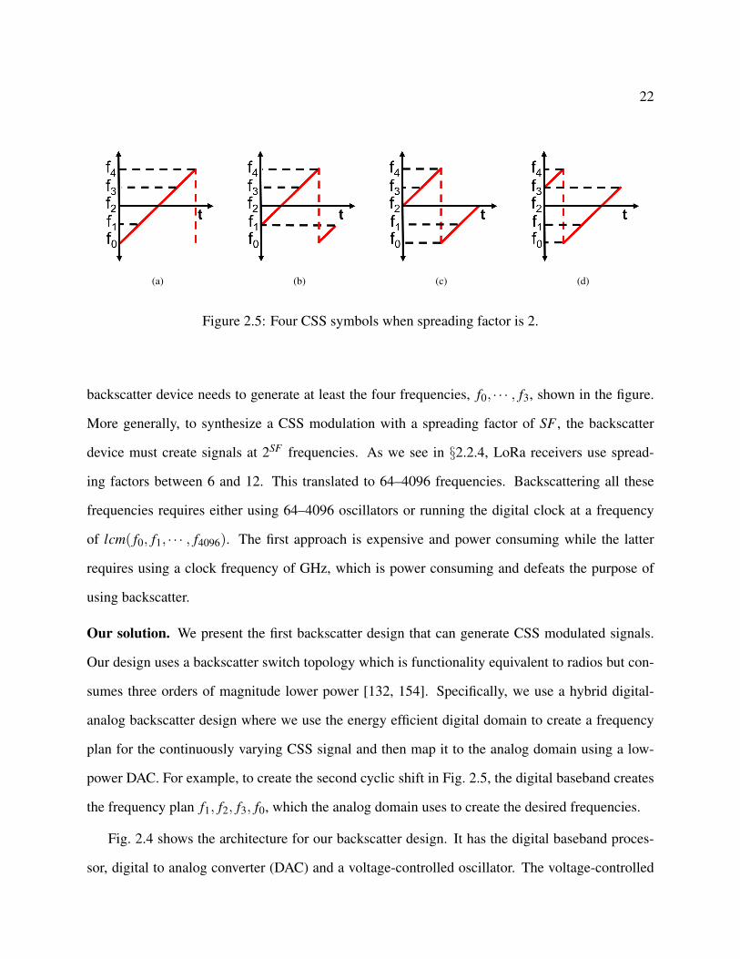
22
(a) (b) (c) (d)
Figure 2.5: Four CSS symbols when spreading factor is 2.
backscatter device needs to generate at least the four frequencies, f0, · · · , f3, shown in the figure.
More generally, to synthesize a CSS modulation with a spreading factor of SF , the backscatter
device must create signals at 2SF frequencies. As we see in §2.2.4, LoRa receivers use spread-
ing factors between 6 and 12. This translated to 64–4096 frequencies. Backscattering all these
frequencies requires either using 64–4096 oscillators or running the digital clock at a frequency
of lcm( f0, f1, · · · , f4096). The first approach is expensive and power consuming while the latter
requires using a clock frequency of GHz, which is power consuming and defeats the purpose of
using backscatter.
Our solution. We present the first backscatter design that can generate CSS modulated signals.
Our design uses a backscatter switch topology which is functionality equivalent to radios but con-
sumes three orders of magnitude lower power [132, 154]. Specifically, we use a hybrid digital-
analog backscatter design where we use the energy efficient digital domain to create a frequency
plan for the continuously varying CSS signal and then map it to the analog domain using a low-
power DAC. For example, to create the second cyclic shift in Fig. 2.5, the digital baseband creates
the frequency plan f1, f2, f3, f0, which the analog domain uses to create the desired frequencies.
Fig. 2.4 shows the architecture for our backscatter design. It has the digital baseband proces-
sor, digital to analog converter (DAC) and a voltage-controlled oscillator. The voltage-controlled

23
oscillator (VCO) is a device that outputs a clock with a frequency that is proportional to the input
voltage. We vary the frequency output of the oscillator by using the DAC to generate the appro-
priate voltages. Specifically, the digital baseband processor outputs an SF bit number, where SF
is the CSS spreading factor. This allows us to output 2SF voltage levels at the output of the SF-bit
DAC. The analog voltage output of the DAC controls the frequency of the VCO.
The challenge however, is that, as shown in figs. 2.3a and 2.3b, in a CSS encoded packet, the
frequency of the signal varies from a negative frequency (−BW2 ) to a positive frequency (BW
2 ). A
voltage-controlled oscillator however only outputs signals at positive frequency. So, we need a
mechanism to synthesize negative frequencies using backscatter. From basic communication the-
ory, negative frequencies essentially can be written as complex signals. Specifically, the complex
exponent, e j2π(± f )t can be written as cos2π f t± jsin2π f t. Thus, generating negative frequencies
requires us to generate both the in-phase cosine signal as well as the out-of-phase sine signal at the
desired frequencies. To do this, existing solutions approximate the sine and cosine signals using
the square wave output by the VCO. This however results in out-of-band harmonics. In the next
section, we describe our harmonic cancellation mechanism.
We note that the receiver receives both the single-tone signal from the RF source as well as
the backscattered LoRa packets. Since the backscatter signal is much weaker, the single-tone
creates in-band interference. To address this, we shift the single-tone outside the desired band and
transform it into out-of-band interference. At a high level, if the RF source transmits the single-
tone signal e2π fct and the backscatter signal generates the complex signal, e2π(∆ f+ fLoRa)t , then the
resulting backscattered RF signal is e2π(( fc+∆ f )+ fLoRa)t . Here ∆ f is a small fixed offset and fLoRa is
the varying frequency corresponding to the baseband LoRa modulation. The above equation shows
that by using a small frequency offset, ∆ f , we can create the LoRa signals in a band centered at
fc +∆ f which is different from that of the single tone, fc.

24
2.2.3 Backscatter Harmonic Cancellation
As described earlier, prior backscatter designs [96, 102] use square waves to approximate sine and
cosine waves which results in harmonics. To understand why this happens, we recall that a square
wave at a rate of ∆ f can be written as a sum of cosine waves using the following expression:
Square(∆ f t) =4π
∞
∑n=0
12n+1
cos(2π (2n+1)∆ f t)
If the RF source transmits cos(2π fct) and the backscatter device is switching with a square
wave operating at ∆ f frequency, signal transmitted by the backscatter device can be written as
cos(2π fct)Square(∆ f ). As a result, in addition to generating the desired signal at fc +∆ f , the
above operation also generates the mirror copy at fc−∆ f , 9.5 dB lower harmonic at fc± 3∆ f ,
15 dB lower harmonic at fc± 5∆ f and additional lower power harmonics. Recent work [96] has
demonstrated how one can eliminate the mirror copy being generated at fc−∆ f using single side
band backscatter technique. However, this technique still preserves the third, fifth and other odd
order harmonics. The third and fifth order harmonics are only 9.5 and 15 dB lower than the desired
backscattered signal and hence create interference on the wireless channel. More importantly, since
the LoRa protocol has very low sensitivities, LoRa devices operating in channels overlapping with
the third and fifth harmonics experience in-band interference from backscatter devices.
Our Solution. Our insight is to use a different signal from the square wave to approximate a
cosine and sine wave. On a high level, one can think of an analog signal as a discrete signal with
infinite distinct voltage levels and smooth transitions, which results in a clean spectrum without any
harmonics. However, square wave has only two levels with discontinuous step transitions, which
results in high frequency components. Our key idea with harmonic cancellation is to introduce
additional voltage levels to better approximate a sinusoidal signal, by imitating radios [152, 130],
and obtain a cleaner frequency spectrum.
25
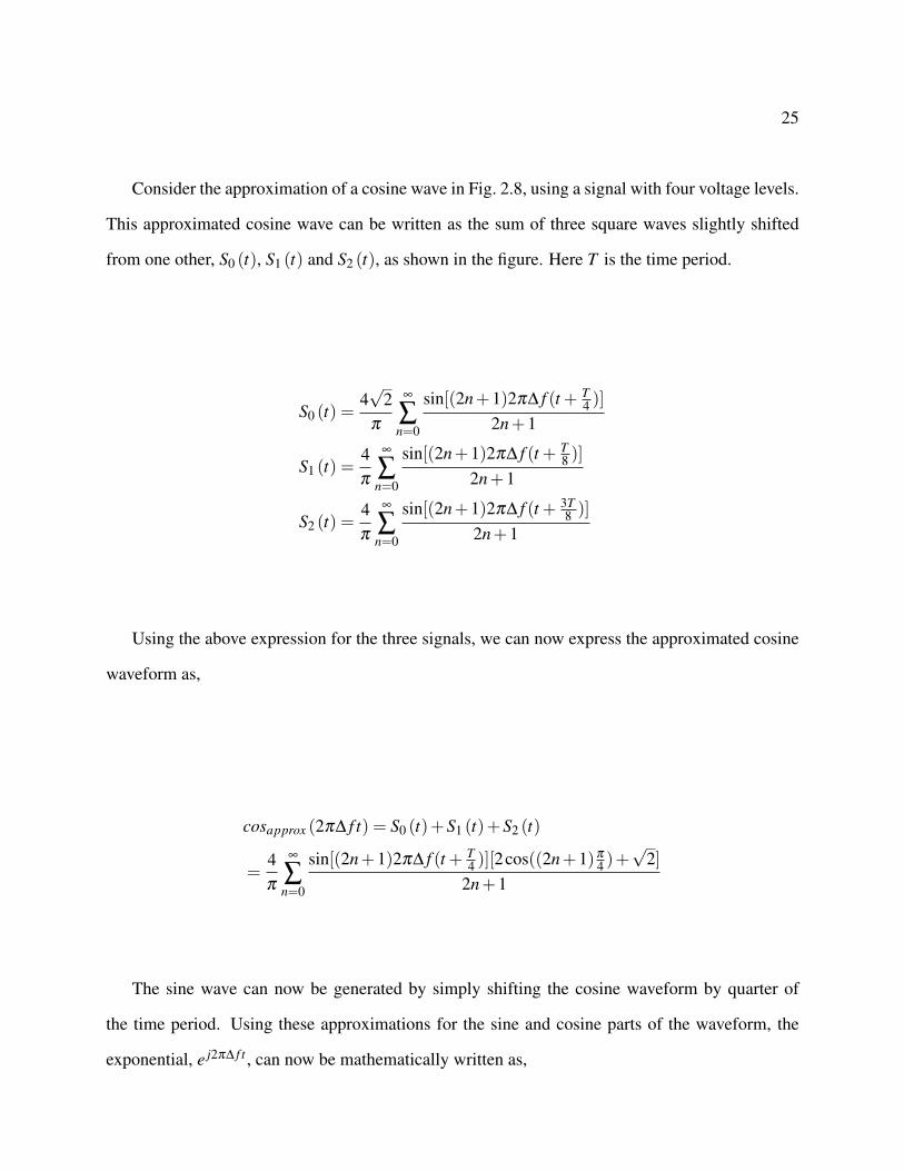
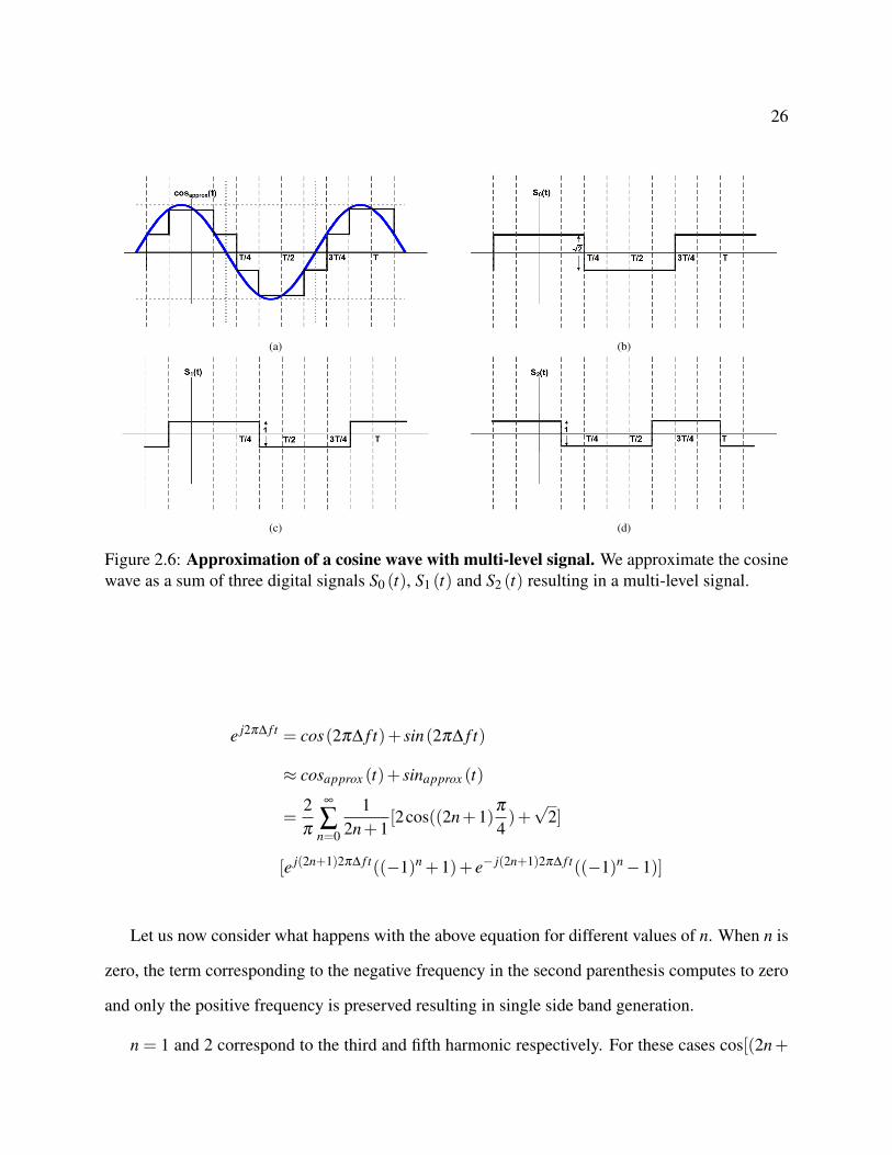
Consider the approximation of a cosine wave in Fig. 2.8, using a signal with four voltage levels.
This approximated cosine wave can be written as the sum of three square waves slightly shifted
from one other, S0 (t), S1 (t) and S2 (t), as shown in the figure. Here T is the time period.
S0 (t) =4√
2π
∞
∑n=0
sin[(2n+1)2π∆ f (t + T4 )]
2n+1
S1 (t) =4π
∞
∑n=0
sin[(2n+1)2π∆ f (t + T8 )]
2n+1
S2 (t) =4π
∞
∑n=0
sin[(2n+1)2π∆ f (t + 3T8 )]
2n+1
Using the above expression for the three signals, we can now express the approximated cosine
waveform as,
cosapprox (2π∆ f t) = S0 (t)+S1 (t)+S2 (t)
=4π
∞
∑n=0
sin[(2n+1)2π∆ f (t + T4 )][2cos((2n+1)π
4 )+√
2]2n+1
The sine wave can now be generated by simply shifting the cosine waveform by quarter of
the time period. Using these approximations for the sine and cosine parts of the waveform, the
exponential, e j2π∆ f t , can now be mathematically written as,
26
(a) (b)
(c) (d)
Figure 2.6: Approximation of a cosine wave with multi-level signal. We approximate the cosinewave as a sum of three digital signals S0 (t), S1 (t) and S2 (t) resulting in a multi-level signal.
e j2π∆ f t = cos(2π∆ f t)+ sin(2π∆ f t)
≈ cosapprox (t)+ sinapprox (t)
=2π
∞
∑n=0
12n+1
[2cos((2n+1)π
4)+√
2]
[e j(2n+1)2π∆ f t((−1)n +1)+ e− j(2n+1)2π∆ f t((−1)n−1)]
Let us now consider what happens with the above equation for different values of n. When n is
zero, the term corresponding to the negative frequency in the second parenthesis computes to zero
and only the positive frequency is preserved resulting in single side band generation.
n = 1 and 2 correspond to the third and fifth harmonic respectively. For these cases cos[(2n+

27
1)π
4 ] =−√
22 and so the above equation computes to zero cancelling the third and fifth harmonics.
Thus, by using the above four level signal, we can cancel the third and fifth harmonics as well
as achieve single sideband modulation at the same time. More generally, when n is of the form
(8k+ 3) and (8k+ 5), cos[(2n+ 1)π
4 ] =−√
22 and hence all the corresponding harmonics will be
cancelled. In summary, the four-level approximated exponential signal cancels at least the third
and fifth order harmonics.
If required, subsequent harmonics can be cancelled by adding more levels. Specifically, addi-
tion of each level cancels the next higher order harmonic. For example, five voltage levels can-
cel the seventh harmonic and ninth harmonic is cancelled with six voltage levels. Finally, every
backscatter switch has a finite delay, which provided additional filtering and automatically sup-
presses higher order harmonics (greater than 9), without the need for additional levels.
In our implementation, we use four levels to cancel the third and fifth order harmonics. We gen-
erate the approximated signals on the backscatter device in the digital domain. The four-level co-
sine signal takes one of four values 0.9239,0.3827,−0.3827,−0.9239. Fixing the cosine value,
lets the sine take one of two values. Thus, the exponential e j2π∆ f t can take one of eight complex
values. We create these complex values by leveraging existing backscatter techniques [144, 96]
that change the impedance connected to the antenna. Fig. 2.4 shows the architecture of our sys-
tem where we switch the antenna between eight different complex impedance values to generate
the eight complex values corresponding to our exponential signal. Specifically, we implement the
exponential wave approximation in a digital logic block called the switch mapper. It takes as input
the eight phases of the VCO output to correspond to the time instances when waveform S0, S1 and
S2 and their time shifted versions (corresponding to the sine wave) undergo transitions. We gener-
ate the eight phases of the clock signal by just shifting the signal in one-eighth of the time period
increments and the switch mapper outputs the 3 control bits which toggle the switch between 8
impedance values to generate the approximate exponential wave. Using this technique, we can

28
successfully cancel the mirror image as well as the third and fifth harmonics, thereby improving
the spectral efficiency of backscatter systems.
2.2.4 Synthesizing LoRa Packets
LoRa achieves its high sensitivity numbers using CSS modulation. The physical layer specifica-
tion for LoRa however is proprietary and is not publicly available. So, we reverse-engineer the
LoRa physical layer using the patents filed by Semtech [135, 73], which is the key LoRa chipset
manufacturer. We also use the Semtech 1276 starter kit [43] that provides an interface to transmit
LoRa packets with various bitrates and an arbitrary payload. Finally, we analyze the transmissions
from the LoRa chipsets on a USRP.
Packet Structure. Fig. 2.7 shows the structure of a LoRa packet, in the form of a spectrogram.
The figure shows a sequence of repeating chirps at the beginning to represent the preamble. LoRa
supports a variable length preamble between 6 and 65535 chirp symbols. To convey the end of the
preamble to the receiver, the preamble ends with synchronization symbols and two and a quarter
down-chirp symbols where the chirp goes from the positive to negative frequency. After down-
chirps, the packet has an optional header with information about the bit rate used. This is followed
by a CSS-encoded payload. An optional 16-bit CRC is send at the end of the packet.
Bit Rates. LoRa bit rates depend on three parameters: the error correction coding rate, chirp
bandwidth and spreading factor. LoRa supports four different hamming code rates and eight chirp
bandwidths of 7.8 kHz, 10.4 kHz, 20.8 kHz, 31.25 kHz, 62.5 kHz, 125 kHz, 250 kHz and 500 kHz.
Further, the spreading factor can be set independently to one of seven values: 6, 7, 8, 9, 10, 11 and
12. The LoRa hardware allows these three parameters to be independently modified resulting in a
total of 224-bit rate settings between 11 bps and 37.5 kbps.
We use the above packet format to synthesize LoRa packets with backscatter. We note the
following.

29
Figure 2.7: LoRa packet structure.
LoRa bandwidth and spreading factor are set a-priori and assumed known at the transmitter and
receiver. The header can include information about the bit rate and payload size used, but is
optional and its overhead can be reduced by statically configuring these parameters, which we do
in our backscatter system.
To achieve a high sensitivity, the phase of the LoRa chirps has to change continuously with time
and has the same value at the beginning and the end of the chirp [135, 73]. To achieve this with
backscatter, at each frequency, we increase the phase by 2π
SF . This ensures that the phase at the
beginning and end of each chirp symbol is the same and so we can maintain phase continuity
across chirp symbols.
To comply with FCC regulations, LoRa uses frequency hopping while using lower-data rate trans-
missions that occupy significant amounts of time on the channel. Specifically, while using a
chirp bandwidth of 125 kHz, LoRa divides the 900 MHz ISM band into 64 channels starting at
902.3 MHz, with increments of 200 kHz. Similarly, with a chirp bandwidth of 500 kHz, LoRa
divides the band into 8 channels in increments of 1.6 MHz. The transmitter performs frequency
hopping between these channels to transmit data to be compliant with FCC. For backscatter, FCC
only regulates the signal source and not the backscatter device [40]2. Thus, we instead hop the
frequency of the single-tone transmitter. The backscatter device however uses the same frequency
offset, ∆ f and is oblivious to this frequency hopping mechanism. To ensure that the backscat-
2As a result, RFID tags do not have an FCC ID, while RFID readers have to get approved by FCC and have anFCC ID.
30
tered LoRa transmissions always lie in the LoRa channels, we hop the frequency of the single-tone
source at a constant frequency offset of ∆ f from the LoRa channels. Specifically, to generate the
backscatter signals at the LoRa channels, f1, f2, · · · , fn, the single-tone source performs frequency
hopping across f1−∆ f , f2−∆ f , · · · , fn−∆ f .
2.2.5 Link-Layer Protocol
We describe how the RF source arbitrates the channel between backscatter devices. Then we
explore concurrent transmissions from multiple backscatter devices.
Arbitrating the channel between backscatter devices. At a high level, we use TDMA to allocate
the wireless channel between different backscatter devices. Specifically, the RF source divides
time into slots and transmits the single tone signal once in each slot. Each backscatter device only
transmits during its assigned slot.
The above protocol requires the backscatter devices to detect the beginning of the single tone
from the RF source. To do this, our design uses existing energy detector hardware circuits that
consume between 98 nW and 2.4 µW and can detect input signals as low as -71 dBm [129, 88].
Note that this is larger than the -148 dBm LoRa sensitivity. This is however the power of the RF
source at the backscatter device, while the latter is the power of the backscattered signal at the
LoRa receiver. In all our experiments, the signal strength at the backscatter device was at least
-45 dBm. We note that to improve the accuracy of detecting the signal from the RF source, we can
also use a preamble signal like an alternating ON-OFF keying sequence of energy and no energy.
This reduces the probability of confusing random transmissions in the 900 MHz band for our RF
source.
To synchronize the slots across different backscatter devices, the RF device uses an unique
ON-OFF keying sync pattern at the beginning of the TDMA round robin. This allows devices
to determine the slot boundaries for a whole round-robin duration. We note that the backscatter
31
devices do not need to have their receivers ON all the time. In particular, depending on the appli-
cation, the backscatter device only transmits when it has new data. Similarly, the RF source does
not transmit the single-tone signal during a time slot, if the corresponding backscatter device is not
scheduled.
Concurrent LoRa transmissions using backscatter. So far we assume that only a single backscatter
device can transmit at a time. However, LoRa divides the 900 MHz band into 64 125 kHz LoRa
channels each of which can have a LoRa transmission. Thus, using a single RF source, we can
enable up to 64 backscatter devices to transmit concurrently on different LoRa channels to their
corresponding receivers. Taking it a step further, CSS transmissions that use different spreading
factors on the same LoRa channel are uncorrelated with each other [43]. Thus, in principle, we
can have multiple backscatter devices with different spreading factors use the same LoRa band and
transmit concurrently to their receivers, increasing the overall network throughput.
We note that we can use the energy detector circuit to transmit ACKs on the downlink chan-
nel. However, given the resilience of CSS modulation and the high sensitivity values, performing
application level error correction codes is sufficient to deliver data to the receivers, with a high
probability, without the need for explicit ACKs.
2.3 Hardware Implementation
We first built a proof of concept prototype using commercial off-the shelf (COTS) components and
used it to characterize the performance and operating range of our system. Then, we design an in-
tegrated circuit based on the hybrid analog-digital architecture for harmonic cancellation proposed
in §2.2.2 to quantify its power consumption.
COTS implementation. Our COTS implementation consists of an RF and a baseband subsection.
The RF subsection is implemented on a four layer FR4 substrate and consists of three cascaded
ADG904 [35] switches to create a SP8T switch network. The switch toggles a 2 dBi whip an-
32
tenna [1] across the eight impedance states required for the harmonic cancellation technique. In our
optimized implementation, we use 47 pF , 3.3 nH||82 Ω, 21 nH||680 Ω, 8.2 nH||330 Ω, 1.8 k Ω,
1.5 pF ||56 k Ω, 9.1 pF ||560 Ω and 3.9 pF as our impedance values to achieve the desired complex
values while incurring a loss of only 4 dB in our backscatter switch network.
We implement the baseband subsection using the DE0-CV development board for an Altera
Cyclone V FPGA [3, 7]. We generate CSS modulated packets in digital domain using Verilog
HDL and output square waves corresponding to the real and imaginary components of the signal
to the RF subsection by interfacing the two digital I/Os on the FPGA to the SP8T switch network
through level shifters.
IC design. We present a LoRa backscatter IC design simulated in TSMC 65 nm LP CMOS pro-
cess [32] using industry standard EDA tools. Our IC is composed of three main components:
digital baseband processor, frequency synthesizer and the backscatter switch network.
Baseband Processor. It takes payload data and packet specifications such as spreading factor,
bandwidth and code rate as input and synthesizes the LoRa packet in accordance to the structure
described in §2.2.4. Next, it maps the bits in the packet to a frequency plan that is used by the
frequency synthesizer block to create the chirp spread spectrum signal. We describe the behavioral
model for LoRa packet in Verilog and use Design Compiler by Synopsis [15] to synthesize the
transistor level implementation. Our baseband processor consumes 1.25 µW to generate a LoRa
packet with spreading factor of 12, 31.25 kHz bandwidth and (8,4) hamming code.
Frequency Synthesizer. We integrate the DAC and VCO in Fig. 2.4 into a single frequency syn-
thesizer block. A frequency synthesizer or phase locked loop (PLL) takes a low frequency clock
source as input and up converts it to a higher frequency. The ratio of the output frequency to the
reference frequency is set by a divide ratio. We use the baseband processor output to directly con-
trol the divide ratio of the frequency synthesizer and modulate the output frequency to generate
CSS modulated data. We use Johnson counter to generate the four versions of the clock which are
33
shifted by one eighth of the time period. The four shifted versions and their complements are used
to represent the eight phases of the clock signal. The frequency synthesizer consumes 4.5 µW to
generate 31.25 kHz CSS packets with a spreading factor of 12 and a 3 MHz offset.
Backscatter Switch Network. The backscatter switch network takes the eight phases of the clock
(four time shifted versions and their complements) and maps the eight phases to RF switches
corresponding to their respective impedance values. The switches are implemented using NMOS
transistors that toggle the antenna between eight discrete impedance states consisting of resistors
and capacitors. We limit the impedances to only resistors and capacitors since inductors consume
huge area and are prohibitively expensive in IC’s. This results in a more constraint constellation
map and 3 dB loss in backscattered signal but is a reasonable compromise for low cost. During
active operation, the backscatter switch network consumes 3.5 µW to backscatter CSS modulated
packets at 3 MHz offset. In total, the IC consumes 9.25 µW .
2.3.1 Cost Analysis
Backscatter communication systems consume 3–4 orders of magnitude lower power than their
counterpart radios [102, 96, 84, 134, 2, 144]. This is because instead of using complex and power
hungry analog front end components of radios, backscatter systems use switches to modulate re-
flections. As a result, backscatter systems are not only extremely low power, but also consume
significantly smaller area. This is a key benefit of backscatter systems because for a given technol-
ogy node, the cost is directly proportional to the die area. Since active radios (e.g. Wi-Fi, LoRa,
BLE) are composed of complex and area intensive components such as power amplifiers, mixers,
local oscillators operating at RF frequencies, the RF front end in these systems (excluding the dig-
ital baseband) typically occupies about 10 mm2 of die area [120, 77, 67, 108, 107]. In contrast,
backscatter systems such as RFID tags are much simpler and occupy significantly lower area. The
typical die area for the communication module in RFID based backscatter systems is in the order
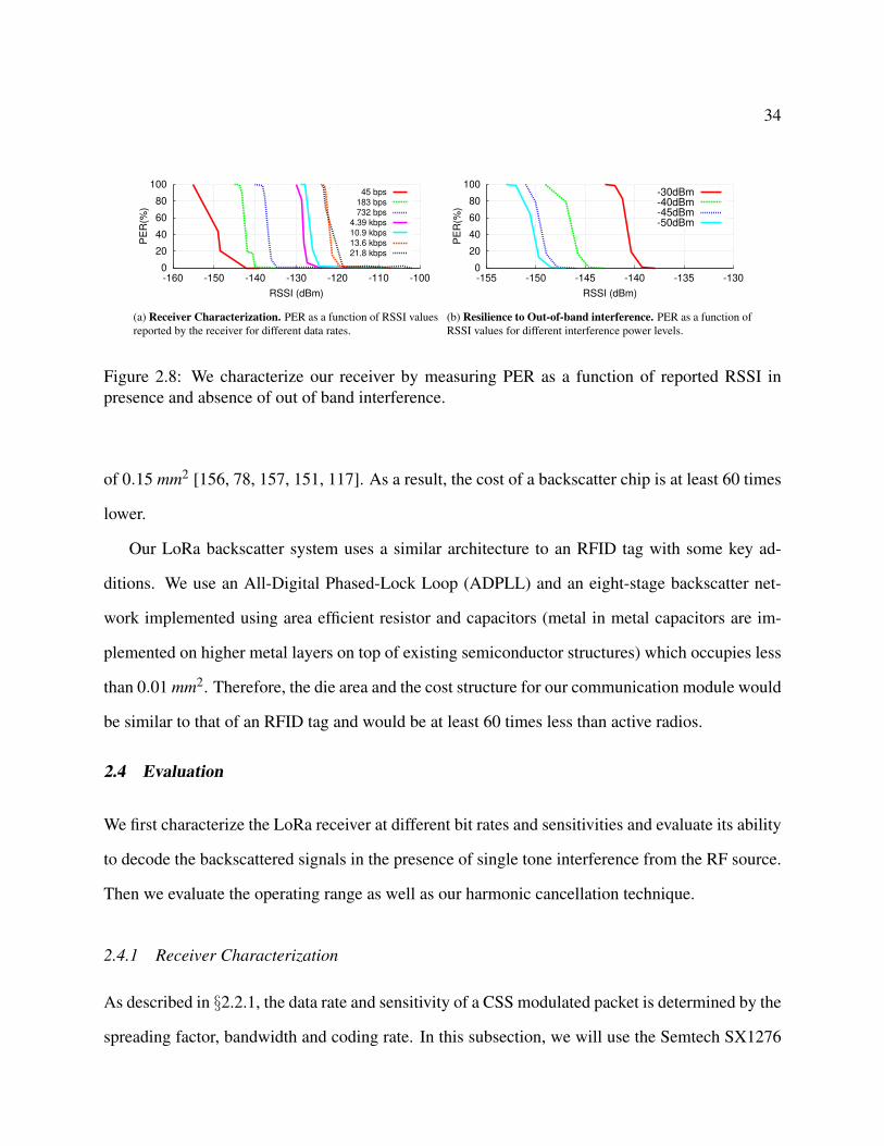
34
0
20
40
60
80
100
-160 -150 -140 -130 -120 -110 -100
PE
R(%
)
RSSI (dBm)
45 bps
183 bps
732 bps
4.39 kbps
10.9 kbps
13.6 kbps
21.8 kbps
(a) Receiver Characterization. PER as a function of RSSI valuesreported by the receiver for different data rates.
0
20
40
60
80
100
-155 -150 -145 -140 -135 -130
PE
R(%
)
RSSI (dBm)
-30dBm-40dBm-45dBm-50dBm
(b) Resilience to Out-of-band interference. PER as a function ofRSSI values for different interference power levels.
Figure 2.8: We characterize our receiver by measuring PER as a function of reported RSSI inpresence and absence of out of band interference.
of 0.15 mm2 [156, 78, 157, 151, 117]. As a result, the cost of a backscatter chip is at least 60 times
lower.
Our LoRa backscatter system uses a similar architecture to an RFID tag with some key ad-
ditions. We use an All-Digital Phased-Lock Loop (ADPLL) and an eight-stage backscatter net-
work implemented using area efficient resistor and capacitors (metal in metal capacitors are im-
plemented on higher metal layers on top of existing semiconductor structures) which occupies less
than 0.01 mm2. Therefore, the die area and the cost structure for our communication module would
be similar to that of an RFID tag and would be at least 60 times less than active radios.
2.4 Evaluation
We first characterize the LoRa receiver at different bit rates and sensitivities and evaluate its ability
to decode the backscattered signals in the presence of single tone interference from the RF source.
Then we evaluate the operating range as well as our harmonic cancellation technique.
2.4.1 Receiver Characterization
As described in §2.2.1, the data rate and sensitivity of a CSS modulated packet is determined by the
spreading factor, bandwidth and coding rate. In this subsection, we will use the Semtech SX1276

35
receiver and evaluate the trade-off between sensitivity and data rates supported by the hardware.
To do this, we use a wired experimental setup to ensure that variations due to multipath do not
impact our results. We use two SX1276 chipsets and configure them to be both the CSS transmitter
and receiver. We connect the antenna port on the two chipsets using variable attenuators and an
RF cable. As described in §2.2.4, LoRa supports 224-bit rate configurations between 11 bps and
37.5 kbps. We implement seven rates spread across 21.8 kbps and 45 bps by picking the appropriate
spreading factor, bandwidth and coding rate. We use variable attenuators to change the power of
the received packet. Specifically, for each of the data rates, we start with a low attenuation value
where we receive all packets and increase the attenuation till we stop receiving all packets. We
transmit 1000 packets with eight-byte payload and two byte CRC and measure the packet error
rate (PER).
Fig. 2.8a plots the PER as a function of the RSSI values reported by the receiver chipset for the
seven data rates. As expected, we observe that the sensitivity is inversely proportional to the data
rate of the packet. For the highest data rate of 21.8 kbps, receiver can decode packets with PER of
less than 1% up to an RSSI value of -119dBm while for the lowest tested data rate of 45 bps we
receive packets down to an RSSI of -142 dBm. Below an RSSI value of -142 dBm, the receiver
cannot correctly decode packets for any of the tested data rates. Finally, we note that similar to
Wi-Fi, the RSSI values reported by the chipset do not correspond to the actual power level of the
received packet. However, the reported RSSI value is a good indicator and is proportional (though
not linear) to the power level of the received packet.
2.4.2 Resilience to Out-of-band interference
Next, we evaluate how well the receiver can decode backscattered packets in the presence of out-
of-band interference from the RF source. Specifically, the RF source transmits at a frequency offset
from the backscatter signal and hence, can create out-of-band interference. To check this, we setup
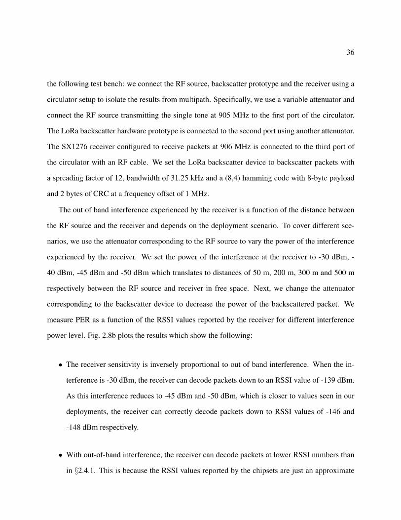
36
the following test bench: we connect the RF source, backscatter prototype and the receiver using a
circulator setup to isolate the results from multipath. Specifically, we use a variable attenuator and
connect the RF source transmitting the single tone at 905 MHz to the first port of the circulator.
The LoRa backscatter hardware prototype is connected to the second port using another attenuator.
The SX1276 receiver configured to receive packets at 906 MHz is connected to the third port of
the circulator with an RF cable. We set the LoRa backscatter device to backscatter packets with
a spreading factor of 12, bandwidth of 31.25 kHz and a (8,4) hamming code with 8-byte payload
and 2 bytes of CRC at a frequency offset of 1 MHz.
The out of band interference experienced by the receiver is a function of the distance between
the RF source and the receiver and depends on the deployment scenario. To cover different sce-
narios, we use the attenuator corresponding to the RF source to vary the power of the interference
experienced by the receiver. We set the power of the interference at the receiver to -30 dBm, -
40 dBm, -45 dBm and -50 dBm which translates to distances of 50 m, 200 m, 300 m and 500 m
respectively between the RF source and receiver in free space. Next, we change the attenuator
corresponding to the backscatter device to decrease the power of the backscattered packet. We
measure PER as a function of the RSSI values reported by the receiver for different interference
power level. Fig. 2.8b plots the results which show the following:
• The receiver sensitivity is inversely proportional to out of band interference. When the in-
terference is -30 dBm, the receiver can decode packets down to an RSSI value of -139 dBm.
As this interference reduces to -45 dBm and -50 dBm, which is closer to values seen in our
deployments, the receiver can correctly decode packets down to RSSI values of -146 and
-148 dBm respectively.
• With out-of-band interference, the receiver can decode packets at lower RSSI numbers than
in §2.4.1. This is because the RSSI values reported by the chipsets are just an approximate

37
-150
-140
-130
-120
-110
0 50 100 150 200 1000
10000
100000
RS
SI
(dB
m)
Bitra
te (
bp
s)
d1 (m)
RSSI (d= 200 m) Bitrate
(a)
-150
-140
-130
-120
-110
0 100 200 300 400 500 100
1000
10000
100000
RS
SI
(dB
m)
Bitra
te (
bp
s)
d1 (m)
RSSI (d= 475 m) Bitrate
(b)
-150
-140
-130
-120
-110
0 100 200 300 400 500 600 10
100
1000
10000
100000
RS
SI
(dB
m)
Bitra
te (
bp
s)
d1 (m)
RSSI (d= 600 m) Bitrate
(c) (d)
Figure 2.9: RSSI in Deployment scenario 1. d is the distance between the RF source and receiver.We move the backscatter device along the line joining them. This figure also shows the correspond-ing LoRa bit rate at which we successfully receive all our ten packets from the backscatter devicewithout any loss.
indicator of link quality and do not represent the absolute measure of power or sensitivity.
• In setup with -40dBm and -50 dBm out of band interference, an offset of 1 MHz at the
backscatter device achieves sensitivities that were within a few dB of the theoretical limit.
We can increase the offset for better sensitivities when facing a higher interference power.
2.4.3 Operational Range
We evaluate the operating range of the LoRa backscatter system in two different scenarios. We use
the SX1276 LoRa development kit connected to a power amplifier as the RF source and configure it
to transmit 30 dBm into a 6 dBi patch antenna at 915 MHz. This is the maximum power permitted
by FCC on the 900 MHz ISM band. We configure the backscatter device to transmit LoRa packets
at a frequency offset of 3 MHz with a spreading factor of 12, bandwidth of 31.25 kHz and a (8,4)
hamming code with 3-byte payload and 2 byte CRC. The SX1276 transceiver chip decodes packets

38
-150
-140
-130
-120
-110
0 500 1000 1500 2000 2500 3000 100
1000
10000
100000
RS
SI
(dB
m)
Bitra
te (
bp
s)
d2 (m)
RSSI (d1= 5 m) Bitrate
(a)
-150
-140
-130
-120
-110
0 500 1000 1500 2000 2500 100
1000
10000
100000
RS
SI
(dB
m)
Bitra
te (
bp
s)
d2 (m)
RSSI (d1= 10 m) Bitrate
(b)
-150
-140
-130
-120
-110
0 500 1000 1500 10
100
1000
10000
100000
RS
SI
(dB
m)
Bitra
te (
bp
s)
d2 (m)
RSSI (d1= 30 m) Bitrate
(c)
Figure 2.10: RSSI in Deployment scenario 2. d1 (d2) is the distance between the backscatterdevice and RF source (receiver). We fix the location of the backscatter device and RF source andmove the receiver away from the backscatter device.
received at 918 MHz and we log the RSSI values for packets that pass CRC.
Deployment scenario 1. The first scenario we consider is a deployment where the RF source and
the receiver are separated from each other and the backscatter device can be at any location between
them. To test this, we place the RF source and the receiver at a distance d, as shown in Fig. 2.9, and
move the backscatter device in a straight line between them. At each location of the backscatter
device, we measure the RSSI value reported by the receiver. Due to the large operating range,
we ran the experiments on a straight road next to open fields. Fig. 2.9 plots the RSSI values for
three different distances between the signal source and the receiver. The x-axis represents d1, the
distance between the RF source and the backscatter device. The plots show the following,
We get a low RSSI when the backscatter device is at the midpoint between the RF source and
the receiver. This is because the signal from the RF source attenuate as 1/d21 before arriving at
the backscatter device. The signals generated by backscattering these attenuated signals further
attenuate as 1/d22 . Thus, the backscatter signal strength at the receiver scales as 1/d2
1d22 which is
minimum when d1 = d2.
Our system operates at all locations up to a maximum separation of 475 m between the RF source
and the receiver. At 600 m, the backscatter device only works close to either the RF source or the
receiver. This shows that our design has an operational range of 475 m.
Deployment scenario 2. In the second scenario, we fix the distance between the backscatter device
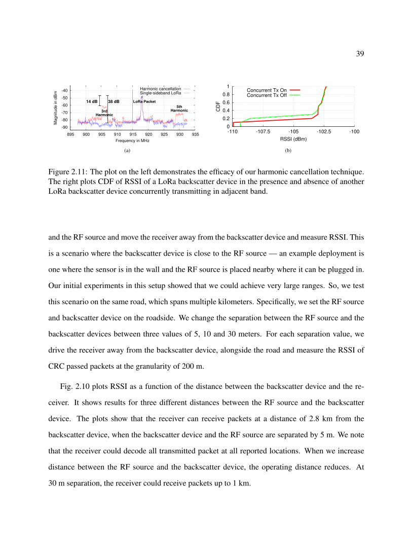
39
-90
-80
-70
-60
-50
-40
895 900 905 910 915 920 925 930 935
Ma
gn
itu
de
in
dB
m
Frequency in MHz
14 dB 38 dB LoRa Packet
3rd
Harmonic
5th
Harmonic
Single-sideband LoRaHarmonic cancellation
(a)
0
0.2
0.4
0.6
0.8
1
-110 -107.5 -105 -102.5 -100
CD
F
RSSI (dBm)
Concurrent Tx OnConcurrent Tx Off
(b)
Figure 2.11: The plot on the left demonstrates the efficacy of our harmonic cancellation technique.The right plots CDF of RSSI of a LoRa backscatter device in the presence and absence of anotherLoRa backscatter device concurrently transmitting in adjacent band.
and the RF source and move the receiver away from the backscatter device and measure RSSI. This
is a scenario where the backscatter device is close to the RF source — an example deployment is
one where the sensor is in the wall and the RF source is placed nearby where it can be plugged in.
Our initial experiments in this setup showed that we could achieve very large ranges. So, we test
this scenario on the same road, which spans multiple kilometers. Specifically, we set the RF source
and backscatter device on the roadside. We change the separation between the RF source and the
backscatter devices between three values of 5, 10 and 30 meters. For each separation value, we
drive the receiver away from the backscatter device, alongside the road and measure the RSSI of
CRC passed packets at the granularity of 200 m.
Fig. 2.10 plots RSSI as a function of the distance between the backscatter device and the re-
ceiver. It shows results for three different distances between the RF source and the backscatter
device. The plots show that the receiver can receive packets at a distance of 2.8 km from the
backscatter device, when the backscatter device and the RF source are separated by 5 m. We note
that the receiver could decode all transmitted packet at all reported locations. When we increase
distance between the RF source and the backscatter device, the operating distance reduces. At
30 m separation, the receiver could receive packets up to 1 km.

40
2.4.4 Efficacy of harmonic cancellation
Next, we evaluate how well our harmonic cancellation technique works in practice. To do this, we
capture the spectrum of the signal generated using our harmonic cancellation backscatter hardware
and compare it to a baseline hardware that does not implement harmonic cancellation. Specifi-
cally, for the baseline we replicate the state-of-the-art single-sideband Wi-Fi hardware from [96]
and adapt it using the techniques in §2.2.2 to generate LoRa packets. We use the Semtech SX1276
development kit to generate the single tone signal at 915 MHz. Since the third and fifth harmon-
ics span a wide band, we use a spectrum analyzer to capture the signal. To avoid interference
from other wireless devices, we connect the Semtech kit to port 1 of a circulator, the backscatter
hardware to port 2 and measure the spectrum of the backscattered signal by connecting a spec-
trum analyzer to the third port of the circulator. We set our backscatter hardware to transmit LoRa
packets with spreading factor of 6, bandwidth of 500 kHz and a (8,4) hamming code with 8-byte
payload and 2 byte CRC at a 3 MHz offset.
The red line in Fig. 2.11a shows the spectrum of the backscattered LoRa packet with the single-
sideband hardware. The plot shows a single tone signal at 915 MHz, which is the RF source and
the desired LoRa packet at 918 MHz. In addition, we see the third and fifth harmonics at 906 MHz
and 930 MHz respectively. These are 14 dB and 22 dB lower than the desired backscatter LoRa
packet. These numbers are 4.7 dB and 7 dB lower than our analysis with square wave in §2.2.2
because in frequency modulated systems, the higher order harmonics are spread across frequency
proportional to the order of the harmonic. Note that the third and fifth harmonics occur on opposite
sides of the desired LoRa transmission at 918 MHz because of single-sideband architecture. The
key observation however is that the third and fifth harmonics create interference in the 900 MHz
band.
The blue line shows the spectrum of the backscattered LoRa packet with our harmonic can-
cellation backscatter hardware. The spectrum shows that the third (906 MHz) and fifth harmonics

41
(930 MHz) are 38 dB lower than the backscattered LoRa packet at 918 MHz and is close to noise.
This demonstrates the efficacy of our harmonic cancellation technique. We note that while in the-
ory we should get perfect cancellation, in practice backscatter hardware built using switches and
passive components have tolerances and variances that introduce small errors.
2.4.5 Concurrent Backscatter Transmissions
Finally, we present a proof-of-concept evaluation of LoRa backscatter when multiple backscatter
devices concurrently transmitting signal from a single RF source. We use two backscatter devices
and configure them to continuously transmit packets at different frequency offsets of 0.75 MHz and
1 MHz. Since the two devices create transmissions on different LoRa bands, they can concurrently
transmit to their receivers. We set the RF source to transmit a single tone at 905 MHz and deploy
the system in a large atrium measuring 104 by 32 feet. We place the RF source and the two receivers
at either ends of the room. We fix the location of the first backscatter device at the center of the
atrium. We move the second backscatter device (operating at 1 MHz offset) across ten different
locations of the atrium. Fig. 2.11b shows the CDF of the RSSI values of packets transmitted by
the first backscatter device in the presence and absence of concurrent transmissions by the second
device. The plots show that concurrent transmissions have negligible impact on the performance
of the first backscatter device.
2.5 Application Deployments
We show two classes of applications enabled by LoRa backscatter. The first set of applications
home/office sensing and precision agriculture leverage the large operational range of our commu-
nication system. We then demonstrate the use of LoRa backscatter in applications with unfavorable
RF propagation conditions such as implantable and epidermal devices. In all our application de-
ployments, we set the backscatter device to transmit with a spreading factor of 12, bandwidth of

42
(a)
0
0.2
0.4
0.6
0.8
1
-150 -145 -140 -135 -130 -125
50 150 500 1500 2500 12500
CD
F
RSSI (dBm)
Bitrate (bps)
(b)
Figure 2.12: Office Deployment. We receive backscattered packets across one floor of an officebuilding with 13,024 f t2 (1210 m2) area.
31.25 kHz and a (8,4) hamming code with three-byte payload and two bytes of CRC. We use the
SX1276 receiver to log the RSSI value of packets that pass the CRC.
2.5.1 Wide-Area Applications
We deploy our system for whole-home sensing.
Whole-Home and Office Sensing. Prior backscatter techniques such as [102, 101] have tried
to replace power-consuming radios in home sensing applications with backscatter but suffer from
limited range and do not provide the coverage required for a practical home deployment. We
deploy our system in a 4,800 f t2 (446 m2) home spread across three floors in a major metropolitan
US city. The layout and floor plan of the house is shown in Fig. 2.13. We put the RF source at
one corner of the house on the third floor and place the receiver in the basement. We move the
backscatter device across the three floors of the occupied house in 6 x 6-foot grid increments and
report RSSI of the received packets at each location.
Fig. 2.13 plots the RSSI of the received backscattered packets at each of the three floors as well
as the outside lawn area. We use a 1 MHz offset on the backscatter device. Our results show that the
across the entire house, our system was able to achieve RSSI values greater than -144 dBm which

43
(a) Basement (b) First floor (c) Second floor
0
0.2
0.4
0.6
0.8
1
-145 -140 -135 -130 -125 -120 -115
150 500 1500 2500 12500 18000 37500
CD
F
RSSI (dBm)
Bitrate (bps)
Basement
First Floor
Second Floor
Outside Lawn
(d) CDF
Figure 2.13: Home Deployment. We receive packets across the 4,800 f t2 (446 m2) house spreadacross three floors.
translates to reliable wireless coverage across the entire house at 45 bps, with a single RF source
and receiver. These rates are sufficient for most home automation devices such as temperature
sensors that transmit small packets sporadically.
Next, we deploy our system with a 3 MHz offset on the backscatter devices in an office space
spanning 13024 f t2 (1210 m2). As shown in Fig. 2.12, the deployment spans 41 offices that are
separated by double sheet-rock (plus insulation) walls with a thickness of approximately 5.7 inch
(14.5 cm). We place a RF source and receiver on the two end of the space as shown in the figure. We
note that the receiver is behind a heavily insulated set of rooms including the restroom and supply
closets with concrete and metal structures separating them. We move the backscatter device into
different offices across the whole floor in 26 by 26-foot grid increments and report the RSSI of
received packets at each location. Fig. 2.12 plots the CDF of the RSSI of received backscattered
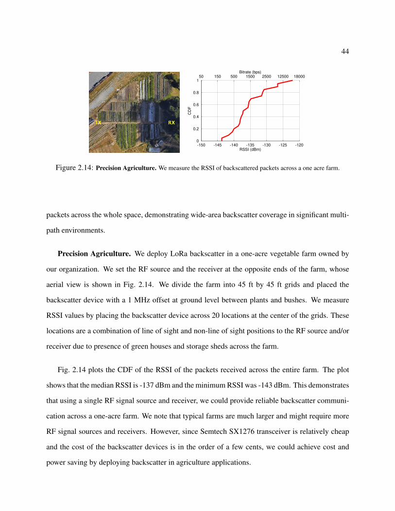
44
0
0.2
0.4
0.6
0.8
1
-150 -145 -140 -135 -130 -125 -120
50 150 500 1500 2500 12500 18000
CD
F
RSSI (dBm)
Bitrate (bps)
Figure 2.14: Precision Agriculture. We measure the RSSI of backscattered packets across a one acre farm.
packets across the whole space, demonstrating wide-area backscatter coverage in significant multi-
path environments.
Precision Agriculture. We deploy LoRa backscatter in a one-acre vegetable farm owned by
our organization. We set the RF source and the receiver at the opposite ends of the farm, whose
aerial view is shown in Fig. 2.14. We divide the farm into 45 ft by 45 ft grids and placed the
backscatter device with a 1 MHz offset at ground level between plants and bushes. We measure
RSSI values by placing the backscatter device across 20 locations at the center of the grids. These
locations are a combination of line of sight and non-line of sight positions to the RF source and/or
receiver due to presence of green houses and storage sheds across the farm.
Fig. 2.14 plots the CDF of the RSSI of the packets received across the entire farm. The plot
shows that the median RSSI is -137 dBm and the minimum RSSI was -143 dBm. This demonstrates
that using a single RF signal source and receiver, we could provide reliable backscatter communi-
cation across a one-acre farm. We note that typical farms are much larger and might require more
RF signal sources and receivers. However, since Semtech SX1276 transceiver is relatively cheap
and the cost of the backscatter devices is in the order of a few cents, we could achieve cost and
power saving by deploying backscatter in agriculture applications.
45
2.5.2 Medical Applications
A key advantage of CSS is its high sensitivity, which enables long-range operation. This sensitivity
also enables long ranges in extremely challenging RF environments such as implantable and body
worn devices.
• Smart Contact Lens. Smart contact lens can measure vital indicators such as glucose,
sodium and cholesterol in tears and enable long term unobtrusive real-time tracking of such
vital parameters [109, 155]. Although progress has been made in miniaturization of the sen-
sor IC, antenna and packaging, real time communication remains a bottleneck [96]. Radio
communication is not applicable since it consumes orders of magnitude higher power than
available on miniature batteries on contact lens form factor devices [123, 70, 109]. Since the
environment is highly unfavorable to RF propagation, only extremely short range backscat-
ter of tens of centimeters has been feasible using both custom hardware [109, 155] and
standards-compliant Wi-Fi/BLE hardware [96]. Such short ranges limit applicability and
renders backscatter less practical.
We leverage LoRa backscatter to demonstrate that a smart contact lens can communicate
using CSS modulated backscatter at orders of magnitude larger distances than was feasible
with prior approaches. We built a contact lens form factor antenna shown in Fig. 2.15a. The
antenna is a 1 cm diameter loop 30 AWG wire encapsulated between two soft contact lenses
for biocompatibility and structural integrity. We immerse the antenna in contact lens solution
and connect it to our COTS prototype.
We deploy the contact lens in a large atrium measuring 104 ft by 32 ft. We place the RF
source and the receiver at the two ends of the room. We set the backscatter device to transmit
LoRa packets at a 1 MHz offset and place the contact lens form factor antenna at the center
of 12 ft by 10 ft grids. We log the reported RSSI value of the received packets at each of the

46
(a) Contact Lens An-tenna Prototype
0
0.2
0.4
0.6
0.8
1
-140 -135 -130 -125 -120 -115
CD
F
RSSI (dBm)
(b) Contact Lens CDF (c) Epidermal Patch Sen-sor Prototype
0
0.2
0.4
0.6
0.8
1
-135 -130 -125 -120 -115 -110 -105
CD
F
RSSI (dBm)
(d) Epidermal Patch Sensor CDF
Figure 2.15: Smart Contact Lens and Flexible epidermal patch sensor. We show the RSSI anddata rate distribution across an entire 3,328 f t2 (309 m2) atrium.
tested locations. Fig. 2.15b plots the CDF of the received RSSI. Our results show reliable
connectivity across the entire atrium, which is order of magnitude larger range than prior
designs [109, 96].
• Flexible Epidermal Patch Sensor. Finally, flexible patch sensors can be used to monitor
temperature, sweat, ECG and other vital signs in real time [70, 124]. These sensors are worn
on the body and are in unfavorable RF environments since the antenna gets significantly
detuned and degrades the link quality.
We use our system to prototype a form factor flexible epidermal patch sensor. To build
our prototype, we use the sticker form factor antenna of an Alien swiggle RFID tag [2]
and connect it to our COTS hardware. Using this approach, we can leverage the cost and
size of RFID tags and create small, inexpensive and reliable epidermal patch sensors. We
use a matching network to tune the impedance of the antenna when it’s in contact with the
human skin. We attach the sticker form factor antenna prototype on a subject’s hand and test
the device across the 3,328 f t2 (309 m2) atrium using the same deployment as the contact
lens prototype with a 1 MHz backscatter offset. Fig. 2.15d plots the CDF of RSSIs for the
received packets. Our results show that we can provide reliable connectivity with an RSSI
greater than -132 dBm.

47
2.5.3 Discussion and Conclusion
We present the first backscatter system that can achieve the ranges required to enable wide-area
communication. In this subsection, we outline avenues for future research.
Achieving higher data rates. Our current design achieves all the bit rates supported by LoRa.
However, an interesting research direction is to achieve higher data rates at the desired ranges
which can be accomplished by using a combination of multiple frequency bands to concurrently
transmit or multiple antenna designs.
LoRa-independent design. A reader might ask a very relevant question: does this technology
depend on the wide adoption of LoRa? The answer is that if LoRa is successful, our technology
can ride on top of its adoption. However, the key component of our wide area backscatter design
is the CSS modulation, which can provide long ranges and high sensitivities independent of LoRa.
Sensitivity to orientation, multipath and obstacles. Unlike RFID and existing backscatter systems
such as Passive Wi-Fi, LoRa backscatter can operate down to sensitivity of -149 dBm and in
the presence of strong in-band and out of band interference. As a result, in typical applications,
LoRa backscatter has sufficient wireless link budget margin which allows it to be robust to signal
loss due to antenna orientation mismatch, multipath and obstacles in the path. We demonstrate
this characteristic of our system by evaluating RF challenging applications such as contact lens,
epidermal patch sensor and wide area deployments such as agriculture, home in §2.5.
Networking LoRa backscatter devices. The focus of this chapter was to design and implement the
LoRa backscatter physical layer. In §2.2.5 we described how LoRa backscatter uses TDMA to
communicate across multiple-backscatter devices. However, since TDMA has an upper bound on
throughput, we address this issue in Chapter 3.
RF Power harvesting. LoRa backscatter is independent of how it is powered. We noted that our
current design can be powered using very small solar cells, button cells as well as printed batteries,

48
given its low power consumption. One can also explore research opportunities for long-range
power harvesting [142] from the RF source.
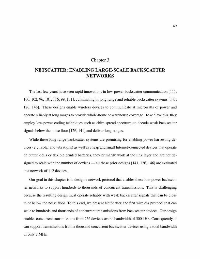
49
Chapter 3
NETSCATTER: ENABLING LARGE-SCALE BACKSCATTERNETWORKS
The last few years have seen rapid innovations in low-power backscatter communication [111,
160, 102, 96, 101, 116, 99, 131], culminating in long range and reliable backscatter systems [141,
126, 146]. These designs enable wireless devices to communicate at microwatts of power and
operate reliably at long ranges to provide whole-home or warehouse coverage. To achieve this, they
employ low-power coding techniques such as chirp spread spectrum, to decode weak backscatter
signals below the noise floor [126, 141] and deliver long ranges.
While these long range backscatter systems are promising for enabling power harvesting de-
vices (e.g., solar and vibrations) as well as cheap and small Internet-connected devices that operate
on button-cells or flexible printed batteries, they primarily work at the link layer and are not de-
signed to scale with the number of devices — all these prior designs [141, 126, 146] are evaluated
in a network of 1–2 devices.
Our goal in this chapter is to design a network protocol that enables these low-power backscat-
ter networks to support hundreds to thousands of concurrent transmissions. This is challenging
because the resulting design must operate reliably with weak backscatter signals that can be close
to or below the noise floor. To this end, we present NetScatter, the first wireless protocol that can
scale to hundreds and thousands of concurrent transmissions from backscatter devices. Our design
enables concurrent transmissions from 256 devices over a bandwidth of 500 kHz. Consequently, it
can support transmissions from a thousand concurrent backscatter devices using a total bandwidth
of only 2 MHz.
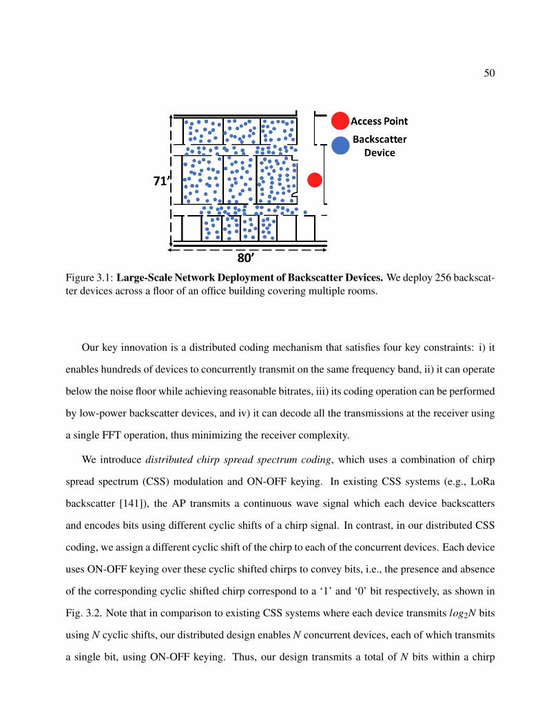
50
Figure 3.1: Large-Scale Network Deployment of Backscatter Devices. We deploy 256 backscat-ter devices across a floor of an office building covering multiple rooms.
Our key innovation is a distributed coding mechanism that satisfies four key constraints: i) it
enables hundreds of devices to concurrently transmit on the same frequency band, ii) it can operate
below the noise floor while achieving reasonable bitrates, iii) its coding operation can be performed
by low-power backscatter devices, and iv) it can decode all the transmissions at the receiver using
a single FFT operation, thus minimizing the receiver complexity.
We introduce distributed chirp spread spectrum coding, which uses a combination of chirp
spread spectrum (CSS) modulation and ON-OFF keying. In existing CSS systems (e.g., LoRa
backscatter [141]), the AP transmits a continuous wave signal which each device backscatters
and encodes bits using different cyclic shifts of a chirp signal. In contrast, in our distributed CSS
coding, we assign a different cyclic shift of the chirp to each of the concurrent devices. Each device
uses ON-OFF keying over these cyclic shifted chirps to convey bits, i.e., the presence and absence
of the corresponding cyclic shifted chirp correspond to a ‘1’ and ‘0’ bit respectively, as shown in
Fig. 3.2. Note that in comparison to existing CSS systems where each device transmits log2N bits
using N cyclic shifts, our distributed design enables N concurrent devices, each of which transmits
a single bit, using ON-OFF keying. Thus, our design transmits a total of N bits within a chirp
51
(a) Existing CSS Modulation (i.e., LoRa)
(b) Our Distributed CSS Coding
Figure 3.2: NetScatter Overview. In traditional CSS systems, a single device uses different cyclicshifts to convey bits. In distributed CSS coding, each cyclic shift is assigned to a different backscat-ter device. Each device then uses the presence and absence of cyclic shift to send ‘1’ and ‘0’ bits.
duration, providing a theoretical gain of Nlog2N .
Our design leverages the fact that creating concurrent cyclic-shifted chirps at a single device
requires distributing its transmit power amongst all the cyclic shifts, which reduces the ability of
the receiver to decode each chirp. Instead we generate concurrent cyclic-shifted chirps across a
distributed set of low-power devices in the network. This allows us to efficiently leverage the
coding gain provided by chirp spread spectrum under the noise floor [71]. Further, we can decode
all the concurrent transmissions using a single FFT operation, since cyclic shifting the chirps in the
time domain translates to offsets in the frequency domain.
Using the above distributed coding mechanism in practice, however, is challenging for two key
reasons.
• Near-far problem. A fundamental problem with enabling concurrent transmissions is that
52
signals from a nearby backscatter device can overpower a farther concurrent device. To
address this issue, we introduce two main techniques. First, we present a power-aware cyclic
shift allocation technique in §3.3.3, where lower SNR devices use much different cyclic shifts
than higher SNR devices. We show that such an allocation can allow backscatter devices that
have an SNR difference of up to 35 dB to be concurrently decoded. Second, to account for
channel variations over time, we develop a zero-overhead power adaptation algorithm where
backscatter devices use reciprocity to estimate their SNR at the AP, using the signal strength
of the AP’s query message. The backscatter devices then adjust their transmission power
to fall within the tolerable SNR difference. Since this calibration is done independently at
each backscatter device using the AP’s query, it does not require additional communication
overhead at the AP.
• Timing synchronization. The above design requires all the devices to start transmitting at the
same time so as to enable concurrent decoding. However, hardware variations and propaga-
tion delays of different devices can make it challenging for hundreds of devices to be tightly
synchronized in time. To avoid this coordination overhead, we leave gaps between cyclic
shifts to ensure that concurrent devices can be decoded. We explore the trade-off between
the required gaps and the chirp bandwidths in §3.3.1.
We implement NetScatter on a testbed of backscatter devices. We create backscatter hardware
that implements NetScatter and includes circuits to perform automatic power adaptation before
each transmission. We deploy our backscatter testbed with 256 devices in an office building span-
ning multiple rooms as shown in Fig. 3.1. We implement our receiver algorithm using USRP
X-300 software-defined radios. Our results reveal that over a 256 node backscatter deployment,
NetScatter achieves a 14–62x gain over prior long-range backscatter systems [141] for its end-to-
end link layer data rates. The key benefit however is in the network latency which sees a reduction
of 15–67x.

53
(a) (b) (c)
Figure 3.3: CSS Primer. We show upchirp and downchirp symbols and FFT results of their mul-tiplication. (a) Baseline upchirp symbol, (b) frequency shifted upchirp symbol and (c) cyclicallyshifted upchirp symbol.
Contributions. This work demonstrates, to the best of our knowledge, the first network protocol
that achieves orders of magnitude more concurrent transmissions than existing backscatter systems.
The closest work to our design is Choir [83] in the radio domain, which decodes concurrent trans-
missions from 5–10 LoRa radios at a software radio. Choir leverages frequency imperfections to
disambiguate between LoRa radios. However, backscatter devices achieve low-power operations
by running at a lower frequency (1-10 MHz) than radios (900 MHz) and thus have much smaller
frequency differences between backscatter devices. This severely limits the ability to rely on fre-
quency imperfections to disambiguate between a large number of backscatter devices (see §3.1.2).
In contrast, our distributed chirp spread spectrum coding mechanism provides a systematic ap-
proach to enable large scale backscatter networks.
3.1 CSS Primer & Existing Approaches
3.1.1 Primer on Chirp Spread Spectrum
In CSS, data is modulated using linearly increasing frequency signals or upchirps. The receiver
demodulates these symbols in a two step process. First, it de-spreads these upchirp symbols by
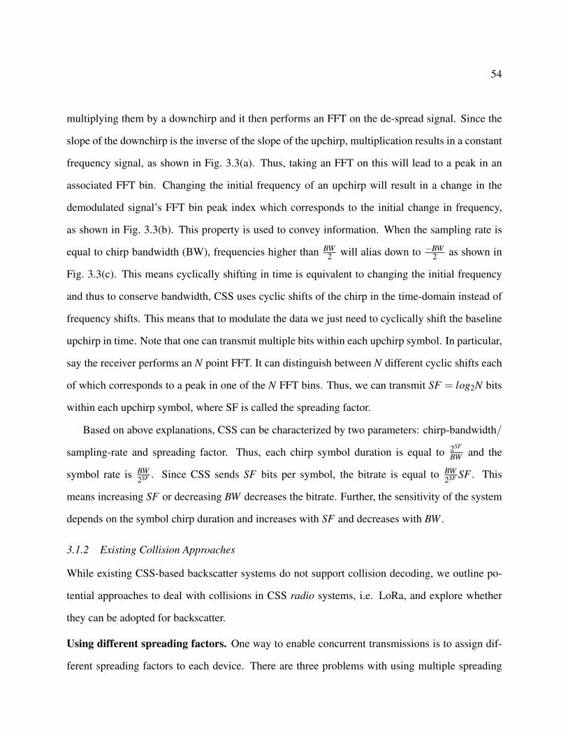
54
multiplying them by a downchirp and it then performs an FFT on the de-spread signal. Since the
slope of the downchirp is the inverse of the slope of the upchirp, multiplication results in a constant
frequency signal, as shown in Fig. 3.3(a). Thus, taking an FFT on this will lead to a peak in an
associated FFT bin. Changing the initial frequency of an upchirp will result in a change in the
demodulated signal’s FFT bin peak index which corresponds to the initial change in frequency,
as shown in Fig. 3.3(b). This property is used to convey information. When the sampling rate is
equal to chirp bandwidth (BW), frequencies higher than BW2 will alias down to −BW
2 as shown in
Fig. 3.3(c). This means cyclically shifting in time is equivalent to changing the initial frequency
and thus to conserve bandwidth, CSS uses cyclic shifts of the chirp in the time-domain instead of
frequency shifts. This means that to modulate the data we just need to cyclically shift the baseline
upchirp in time. Note that one can transmit multiple bits within each upchirp symbol. In particular,
say the receiver performs an N point FFT. It can distinguish between N different cyclic shifts each
of which corresponds to a peak in one of the N FFT bins. Thus, we can transmit SF = log2N bits
within each upchirp symbol, where SF is called the spreading factor.
Based on above explanations, CSS can be characterized by two parameters: chirp-bandwidth/
sampling-rate and spreading factor. Thus, each chirp symbol duration is equal to 2SF
BW and the
symbol rate is BW2SF . Since CSS sends SF bits per symbol, the bitrate is equal to BW
2SF SF . This
means increasing SF or decreasing BW decreases the bitrate. Further, the sensitivity of the system
depends on the symbol chirp duration and increases with SF and decreases with BW .
3.1.2 Existing Collision Approaches
While existing CSS-based backscatter systems do not support collision decoding, we outline po-
tential approaches to deal with collisions in CSS radio systems, i.e. LoRa, and explore whether
they can be adopted for backscatter.
Using different spreading factors. One way to enable concurrent transmissions is to assign dif-
ferent spreading factors to each device. There are three problems with using multiple spreading
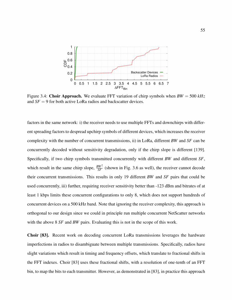
55
0
0.2
0.4
0.6
0.8
1
0 0.5 1 1.5 2 2.5 3 3.5 4 4.5 5 5.5 6 6.5 7
CD
F
∆FFTBin
Backscatter Devices
LoRa Radios
Figure 3.4: Choir Approach. We evaluate FFT variation of chirp symbols when BW = 500 kHzand SF = 9 for both active LoRa radios and backscatter devices.
factors in the same network: i) the receiver needs to use multiple FFTs and downchirps with differ-
ent spreading factors to despread upchirp symbols of different devices, which increases the receiver
complexity with the number of concurrent transmissions, ii) in LoRa, different BW and SF can be
concurrently decoded without sensitivity degradation, only if the chirp slope is different [139].
Specifically, if two chirp symbols transmitted concurrently with different BW and different SF ,
which result in the same chirp slope, BW 2
SF (shown in Fig. 3.6 as well), the receiver cannot decode
their concurrent transmissions. This results in only 19 different BW and SF pairs that could be
used concurrently, iii) further, requiring receiver sensitivity better than -123 dBm and bitrates of at
least 1 kbps limits these concurrent configurations to only 8, which does not support hundreds of
concurrent devices on a 500 kHz band. Note that ignoring the receiver complexity, this approach is
orthogonal to our design since we could in principle run multiple concurrent NetScatter networks
with the above 8 SF and BW pairs. Evaluating this is not in the scope of this work.
Choir [83]. Recent work on decoding concurrent LoRa transmissions leverages the hardware
imperfections in radios to disambiguate between multiple transmissions. Specifically, radios have
slight variations which result in timing and frequency offsets, which translate to fractional shifts in
the FFT indexes. Choir [83] uses these fractional shifts, with a resolution of one-tenth of an FFT
bin, to map the bits to each transmitter. However, as demonstrated in [83], in practice this approach
56
Figure 3.5: Bandwidth Aggregation. Here we use an aggregate bandwidth of 2BW but eachdevice transmits only using BW. Upchirps with different cyclic shifts shown in different colors.Each upchirp is assigned to a device.
does not scale to more than 5 to 10 concurrent devices. To understand this limitation in theory,
consider N concurrent devices. The probability that each of these transmitters has a different FFT
peak index fraction, given the resolution of one-tenth of an FFT bin, is equal to 10!(10−N)!10N . When
N is 5 this probability is only 30%. Moreover, if any two transmitters use the same cyclic shifted
upchirp symbol at the same time, it will result in a collision that cannot be decoded. In the case of
LoRa modulation, if there are N transmitters and assuming each device transmits a random set of
bits during each symbol interval, the probability of two transmitters using the same cyclic shift is
equal to: 1−∏Ni=1(1− i−1
2SF ) which is approximately N(N−1)2SF+1 .
For SF = 9 and N = 10, this probability is around 9%. This means that there is around 9% prob-
ability that within each CSS symbol, two transmitters will use the same upchirp cyclic shift, which
the receiver cannot disambiguate. This probability increases to 32% with 20 devices, preventing
concurrent decoding of a large number of transmitters.
Moreover, Choir is based on oscillator imperfection causing frequency variation on different
devices, and Choir cannot differentiate two concurrent transmissions if both transmissions fall into
same FFT bin fraction. Choir uses an active radio system which generates frequencies in 900 MHz
band. However, since backscatter systems are designed to consume less power and only generate
57
baseband signals, their output frequency is less than 10 MHz. Now, in the ideal scenario where the
same crystal oscillator is used for both radios and backscatter devices, the frequency variation of the
backscatter devices is 90 times smaller than radios and can be even less than 1 FFT bin depending
on the SF and BW . This means a backscatter network cannot use all 10 different FFT bin fractions
that Choir have used. Fig. 3.4 shows CDF of FFT bin variation for our actual backscatter hardware
which are recorded over time. This results show that FFT variation is always less than a third of an
FFT bin. Thus, Choir cannot enable large concurrent transmissions with backscatter.
In conclusion, the desired solution must satisfy three constraints: 1) ability to differentiate
between FFT peaks corresponding to different backscatter devices, 2) ability to associate the FFT
peaks to the corresponding devices, and 3) ensure that two devices do not use the same FFT peak
at the same time. NetScatter design satisfies all these constraints.
3.2 NetScatter Design
3.2.1 Distributed CSS Coding
Our approach is to take advantage of low-power and high sensitivity of CSS modulation to design
a communication and networking system that enables hundreds of backscatter devices to transmit
at the same time.
At a high level, we use a combination of CSS modulation and ON-OFF keying to enable con-
current transmissions. Our intuition is as follows: if we look at the FFT plots of Fig. 3.3, all the
FFT bins except one bin are empty; however these empty bins could be utilized for orthogonal
transmissions. While it is difficult to design low-power backscatter devices that can transmit mul-
tiple cyclic shifts at the same time, we can leverage all these empty bins by having different devices
transmit different shifts and make use of the unused FFT bins. In particular, each device is assigned
to a particular cyclic shifted upchirp symbol. It sends data by either sending the upchirp symbol or
not sending it, i.e., by using ON-OFF keying of its assigned cyclic shifted chirp. Since, there are

58
2SF FFT bins, ideally we can support 2SF concurrent transmissions. This modulation will satisfy
the above three requirements. The peaks can be differentiated and assigned to their corresponding
devices. Moreover, none of them will use the same FFT bin at the same time.
We note the following about our distributed design.
• Receiver complexity. The received signal is composed of multiple transmissions. They can
be demodulated by despreading with a baseline downchirp multiplication and performing an
FFT operation. Then, we can determine the presence and absence of a peak in each FFT
bin and find if the corresponding backscatter device is sending ‘0’ or ‘1’. The key point is
that the process of despreading and performing FFT, which are the major contributors of the
demodulation process and provide a coding gain for each of the backscatter devices enabling
them to operate below the noise floor, are being done once and do not depend on the number
of concurrent transmissions. This means that the receiver complexity is nearly constant with
the number of devices.
• Throughput gain. In our approach, ideally there can be as many as 2SF transmissions at
each symbol period. Since each backscatter device uses ON-OFF keying over a symbol,
their individual data rate is BW2SF . Thus, the aggregate network throughput is equal to BW . In
comparison, LoRa have a throughput of BW2SF SF . Thus, we can achieve a throughput gain of
2SF
SF , which shows that the gain exponentially increases with the SF value used in the system.
This is expected since the number of concurrent devices we can support is an exponential
function of SF, i.e., 2SF .
• NetScatter and CDMA. Our distributed CSS coding can be thought of as code-division
multiplexing mechanism that is low-power and where each of the 2SF cyclic shifts is in an
orthogonal set of codes in a CDMA system. These orthogonal codes are then assigned to
2SF different backscatter devices which enables 2SF concurrent transmissions.

59
Figure 3.6: Timing Mismatch. in detecting beginning of a chirp symbol and its translation to FFTbin variation.
• Gain in the context of Shannon capacity. A key gain we are achieving in our design stems
from using the power across all the concurrent backscatter devices. Specifically we note that
the Shannon capacity of a multi-user network that operates under the noise floor linearly
increases with the number of devices. Said differently, the multi-user capacity of an access
point network is given as [145], C = BW log2(1+NPSPN
). Here BW is the channel bandwidth,
PN and PS are the noise and signal power and N is the number of concurrent devices. At SNRs
below the noise floor, the above equation can be approximated as BWln(2)
NPSPN
, since ln(1+x)≈ x
when x is small. This means that for systems that operate below the noise-floor, the network
capacity scales linearly with the number of users. This linear increase stems from the fact
that the N backscatter devices put in N times more power back to the AP than a single
backscatter device.
• Bandwidth aggregation. The bitrate achieved by each backscatter device in our distributed
design is given by BW2SF and the number of concurrent devices is 2SF . Thus, while we can
increase the number of devices by increasing SF, it would decrease the bitrate of each device.
Thus, to increase both the bitrate and the number of device we should increase the bandwidth,
BW . Say, we want to support twice the number of devices while maintaining the same bitrate
60
by using twice the bandwidth. This can be achieved in two ways. First, we can use two filters
and independently operate two sets of devices across the two bands. This approach requires
two different FFTs to be performed independently across the bands. The second approach is
to use one aggregate band with twice the bandwidth, 2BW , but use the same SF and chirp
BW as before and alias down to −BW whenever the chirp frequency hits the maximum as
shown in Fig. 3.5. To demodulate this signal, we just need to multiply the signal which is
composed of the aggregate band by the downchirp and perform 2×2SF FFT operation once.
The complexity of this method is lower than the former since there is no need to use filters
and separate the bands.
3.3 Addressing Practical Issues
3.3.1 Timing Mismatch
The above design requires all the backscatter devices to be time synchronized. To understand
why, consider two consecutive upchirps being sent by a device, as shown in Fig. 3.6. Now say
that we demodulate the signal in these two timing durations, shown in blue and red, we will get
different FFT peak locations. Specifically, with a ∆t time difference between these durations, the
corresponding FFT bin peak location would change by, ∆FFTbin = ∆tBW . When this change
is greater than a single FFT bin, backscatter devices that are assigned to consecutive cyclic shifts
interfere with each other and cannot be decoded. Thus, all the devices should be time synchronized.
In our design the access point sends a query message telling devices to transmit concurrently. The
devices use this query to synchronize and respond concurrently. First, we explain the sources
of time delay in our system and then we explain our solutions. There are multiple factors that
can contribute to time delays introduced in practice and can be different for different backscatter
devices.
61
• Hardware delay. Unlike Wi-Fi devices which use much higher clock frequencies for pro-
cessors, backscatter devices use low-power microcontrollers (MCUs) that can introduce a
variable delay into the system. For backscatter devices, the source of these hardware delay
variations come from the time the envelope detector receives the query message from the
access point, communicates it to the MCU and then the device backscatters the chirp signal.
As we show in §3.5.2, this hardware delay variations can be as high as 3.5 µs, which can
translate to more than one FFT bin at 500 kHz bandwidth.
• Propagation delay and multipath. Since backscatter devices can be at different distances
to the access point, their time of flight (TOF) can be different. However, since our target
application is for whole-home or warehouse sensing, the propagation distance is less than
100 m which translates to a ToF < 666ns = 2×1003×108 and corresponds to only a 0.33 FFT bin
change, assuming a bandwidth of 500 kHz. The multipath delay spread for indoor environ-
ments is between 50 to 300 ns [133, 81]. For 500 kHz, this delay spread translates to less
than 0.15 FFT bin change, which is negligible.
Our solution: Bandwidth-based cyclic-shift assignment. Hardware delay variations over time
are hard to correct for. As described above, by nature of operating on MCUs and other low-power
computational platforms, these devices have a hardware delay variation over time that changes
between packets. Our solution to this problem is to put a few empty FFT bins adjacent to each FFT
bin assigned to a device. That is, if FFT bin i is assigned to a device, the adjacent SKIP− 1 FFT
bins are empty and not assigned to any device. This can be done by using only every SKIPth cyclic
shift of the chirp. This ensures that the hardware delay does not result in interference between
adjacent devices.
Achieving such an assignment requires us to answer the following key question: how do we
pick the value SKIP? As described earlier, given the hardware delay variation ∆t, the shift in the

62
Table 3.1: NetScatter Different Modulation Configurations, with maximum time/freq. mis-match that can be tolerated.
BW[kHz]
SF TimeVariation
FrequencyVariation
Bit Rate[bps]
Sensitivity[dBm]
500 9 2 µs 976 Hz 976 -123500 8 2 µs 1953 Hz 1953 -120250 8 4 µs 976 Hz 976 -123250 7 4 µs 1953 Hz 1953 -120125 7 8 µs 976 Hz 976 -123125 6 8 µs 1953 Hz 1953 -118
number of FFT bins is ∆tBW . This means that there is a trade-off in our system regarding the total
network throughput, bitrate for each device and sensitivity. In particular, increasing BW increases
the number of FFT bins that have to be left empty and decreases the total network throughput.
On the other hand, decreasing BW reduces the number of FFT bins but decreases the bitrate per
device with the same SF . To compensate for the decreased device’s bitrate, we can decrease the
SF . Note that, we can choose total bandwidth, chirp BW and SF of the system by considering the
hardware delay variations, required bitrate per device, sensitivity for each device and total number
of devices. For our implementation, we pick the same total bandwidth and chirp BW of 500 kHz
and SF = 9 which supports around 1 kbps (976 bps) bitrate at each device while ensuring that the
number of empty bins between devices, SKIP, is two.
3.3.2 Frequency Mismatch
The devices experience frequency offsets because of hardware variations in the crystals used in
their oscillators. As explained in §3.1.1, change in frequency translates to FFT bin change of the
demodulated device packet. This again, causes one device to be misinterpreted as other device.
Considering a bandwidth of BW and spreading factor of SF , the frequency difference between
FFT bins is equal to BW2SF . This means that a ∆ f frequency offset results in a change in the FFT bin
of ∆FFTbin = 2SF ∆ fBW . Therefore, either increasing the spreading factor SF or decreasing the BW
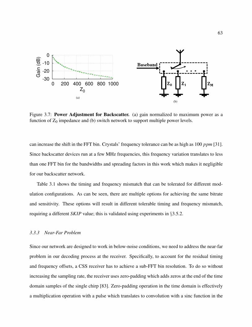
63
-30
-20
-10
0
0 200 400 600 800 1000
Ga
in (
dB
)
Z0
(a)(b)
Figure 3.7: Power Adjustment for Backscatter. (a) gain normalized to maximum power as afunction of Z0 impedance and (b) switch network to support multiple power levels.
can increase the shift in the FFT bin. Crystals’ frequency tolerance can be as high as 100 ppm [31].
Since backscatter devices run at a few MHz frequencies, this frequency variation translates to less
than one FFT bin for the bandwidths and spreading factors in this work which makes it negligible
for our backscatter network.
Table 3.1 shows the timing and frequency mismatch that can be tolerated for different mod-
ulation configurations. As can be seen, there are multiple options for achieving the same bitrate
and sensitivity. These options will result in different tolerable timing and frequency mismatch,
requiring a different SKIP value; this is validated using experiments in §3.5.2.
3.3.3 Near-Far Problem
Since our network are designed to work in below-noise conditions, we need to address the near-far
problem in our decoding process at the receiver. Specifically, to account for the residual timing
and frequency offsets, a CSS receiver has to achieve a sub-FFT bin resolution. To do so without
increasing the sampling rate, the receiver uses zero-padding which adds zeros at the end of the time
domain samples of the single chirp [83]. Zero-padding operation in the time domain is effectively
a multiplication operation with a pulse which translates to convolution with a sinc function in the

64
-50
-40
-30
-20
-10
0
0 640 1280 1920 2560 3200 3840 4480 5120
0 64 128 192 256 320 384 448 512
Po
we
r (d
B)
FFT Bin
SKIP
High Power Low Power High Power
∗ (SKIP=2,-13dB)
∗ (SKIP=3,-21dB)
Figure 3.8: Normalized Power Spectrum. We show power spectrum of an upchirp multiplied bya baseline downchirp in FFT domain. This plot shows the main lobe and side lobes of a singlechirp transmission. We assign devices to high and low power regions based on their power level.
FFT domain. This makes it easier to locate the FFT peak location. However, convolving with a
sinc function introduces side lobes as shown in Fig. 3.8. Assume that there are two devices with
cyclic shifts C1 = 0 and C2. If the power of C2 is lower than power of C1’s side lobes, it cannot be
decoded.
Our solution. To address this issue, we propose two techniques that work together to increase our
dynamic range.
Coarse-grained power-aware cyclic shift assignment. Our intuition here is as follows: Fig. 3.8
suggests that we should assign adjacent FFT bins to devices that have a small SNR difference.
In particular, when SKIP is 2, for two neighboring backscatter devices with an SNR difference
greater than 13 dB, the lower power device cannot be decoded. Further, it shows that the side-lobe
power of a high SNR device decreases as we go to farther FFT bins. Thus, we need to ensure that a
lower SNR device has to correspond to FFT bins that are farther from the FFT bins corresponding
to higher SNR devices. This ensures that the side-lobes of the high-SNR device do not affect the
decoding of the low-SNR devices. Specifically, we assign different cyclic shifts to different devices
at association phase to ensure that the FFT bins corresponding to the lower-SNR devices are close
to each other and are far from higher-SNR devices. To do this, the AP computes the signal strength

65
of the incoming device in the association phase (see §3.4.2) and assigns its cyclic shift based on its
signal strength and also the strengths of the devices that are already in the network.
We run simulations to understand the benefits of this allocation. Specifically, we assign two
devices to FFT bins 2 and 258, with SF = 9 and BW = 500 kHz. To be realistic, we added Gaussian
frequency mismatch with variance of 300 Hz to each device to account for timing and frequency
mismatches between them. We change the power of the second device and measure the bit error
rate (BER) for the first device. Fig. 3.12 shows the BER over 104 symbols, for different power
differences between the two devices. As can be seen, the BER remains unaffected even when the
second device is around 40 dB stronger than the first device. This shows that our power-aware
allocation can in theory tolerate power difference of 40 dB between devices. In practice however
this is a little lower at 35 dB (see §3.5.3).
Fine-grained self-aware power-adjustment. While the above assignment is determined at asso-
ciation, mobility in the environment and fading will change the SNR of each of the devices over
time (see Fig. 3.9). To address this, each device adjusts its power over time using the signal strength
of the query message from the AP, using three different levels. We define the maximum power of
the device as 0 dB power gain. First, during association, we consider two cases for the associating
device. If it sees a low received signal strength for the AP’s query packet, it sets its power gain to
the maximum. Otherwise, it sets its gain to the middle level. This gives the higher signal strength
backscatter devices leeway to both increase and decrease their power, after association. The AP
uses the resulting backscatter signal strengths during association to assign a corresponding cyclic
shift. The backscatter devices use the signal strength at association as a baseline and either increase
or decrease their power gains for the rest of the concurrent transmissions, i.e., if the signal strength
for the AP’s query message increases (decreases), the backscatter devices decrease (increase) their
power gain. If the device cannot meet its expected SNR requirements given its limited power levels
and assigned cyclic shift, it does not join the concurrent transmissions. If this happens more than
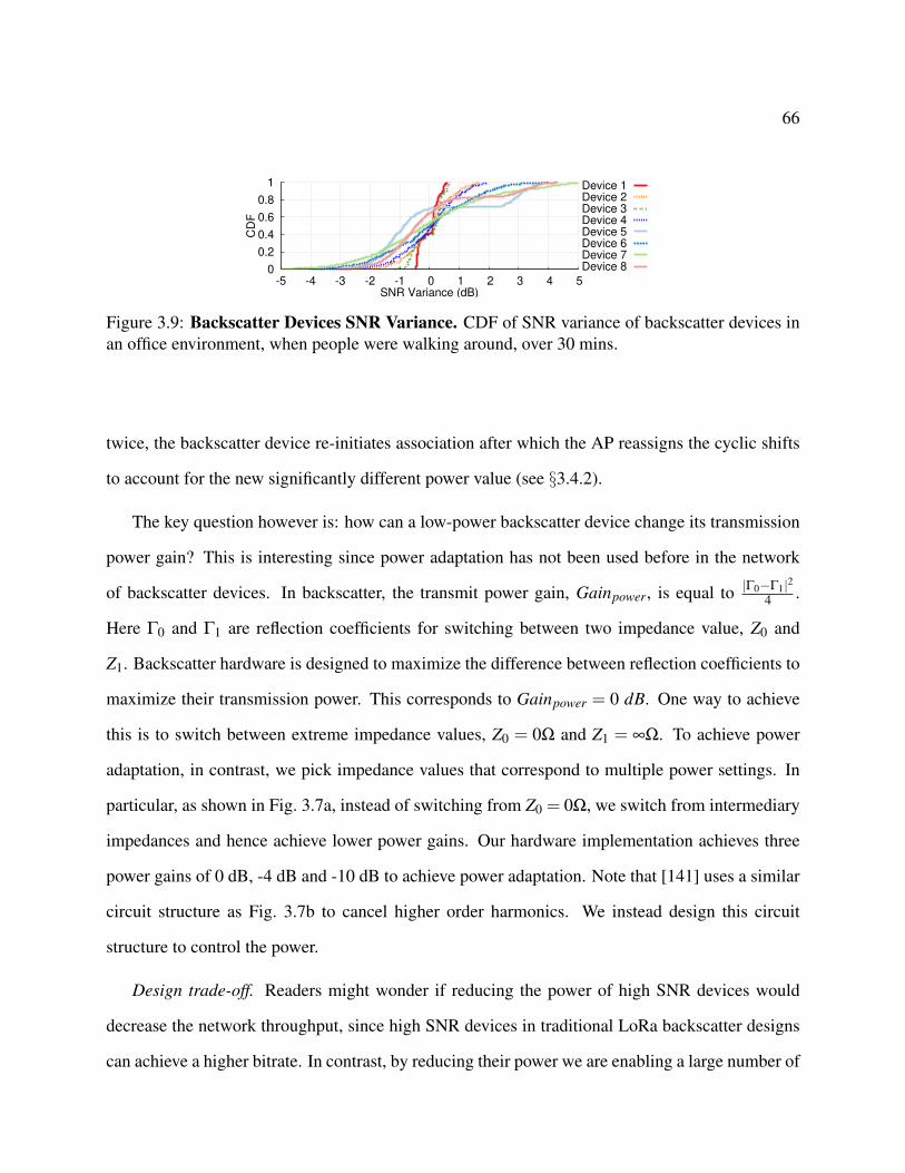
66
0
0.2
0.4
0.6
0.8
1
-5 -4 -3 -2 -1 0 1 2 3 4 5
CD
F
SNR Variance (dB)
Device 1Device 2Device 3Device 4Device 5Device 6Device 7Device 8
Figure 3.9: Backscatter Devices SNR Variance. CDF of SNR variance of backscatter devices inan office environment, when people were walking around, over 30 mins.
twice, the backscatter device re-initiates association after which the AP reassigns the cyclic shifts
to account for the new significantly different power value (see §3.4.2).
The key question however is: how can a low-power backscatter device change its transmission
power gain? This is interesting since power adaptation has not been used before in the network
of backscatter devices. In backscatter, the transmit power gain, Gainpower, is equal to |Γ0−Γ1|24 .
Here Γ0 and Γ1 are reflection coefficients for switching between two impedance value, Z0 and
Z1. Backscatter hardware is designed to maximize the difference between reflection coefficients to
maximize their transmission power. This corresponds to Gainpower = 0 dB. One way to achieve
this is to switch between extreme impedance values, Z0 = 0Ω and Z1 = ∞Ω. To achieve power
adaptation, in contrast, we pick impedance values that correspond to multiple power settings. In
particular, as shown in Fig. 3.7a, instead of switching from Z0 = 0Ω, we switch from intermediary
impedances and hence achieve lower power gains. Our hardware implementation achieves three
power gains of 0 dB, -4 dB and -10 dB to achieve power adaptation. Note that [141] uses a similar
circuit structure as Fig. 3.7b to cancel higher order harmonics. We instead design this circuit
structure to control the power.
Design trade-off. Readers might wonder if reducing the power of high SNR devices would
decrease the network throughput, since high SNR devices in traditional LoRa backscatter designs
can achieve a higher bitrate. In contrast, by reducing their power we are enabling a large number of
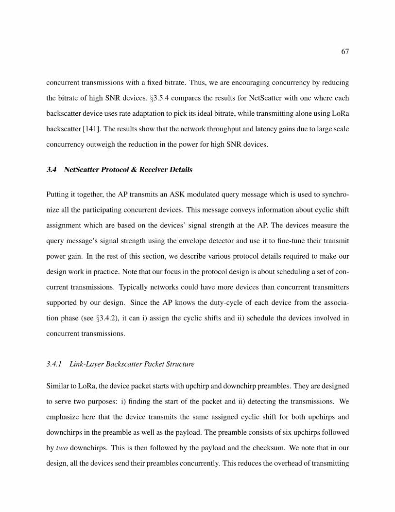
67
concurrent transmissions with a fixed bitrate. Thus, we are encouraging concurrency by reducing
the bitrate of high SNR devices. §3.5.4 compares the results for NetScatter with one where each
backscatter device uses rate adaptation to pick its ideal bitrate, while transmitting alone using LoRa
backscatter [141]. The results show that the network throughput and latency gains due to large scale
concurrency outweigh the reduction in the power for high SNR devices.
3.4 NetScatter Protocol & Receiver Details
Putting it together, the AP transmits an ASK modulated query message which is used to synchro-
nize all the participating concurrent devices. This message conveys information about cyclic shift
assignment which are based on the devices’ signal strength at the AP. The devices measure the
query message’s signal strength using the envelope detector and use it to fine-tune their transmit
power gain. In the rest of this section, we describe various protocol details required to make our
design work in practice. Note that our focus in the protocol design is about scheduling a set of con-
current transmissions. Typically networks could have more devices than concurrent transmitters
supported by our design. Since the AP knows the duty-cycle of each device from the associa-
tion phase (see §3.4.2), it can i) assign the cyclic shifts and ii) schedule the devices involved in
concurrent transmissions.
3.4.1 Link-Layer Backscatter Packet Structure
Similar to LoRa, the device packet starts with upchirp and downchirp preambles. They are designed
to serve two purposes: i) finding the start of the packet and ii) detecting the transmissions. We
emphasize here that the device transmits the same assigned cyclic shift for both upchirps and
downchirps in the preamble as well as the payload. The preamble consists of six upchirps followed
by two downchirps. This is then followed by the payload and the checksum. We note that in our
design, all the devices send their preambles concurrently. This reduces the overhead of transmitting
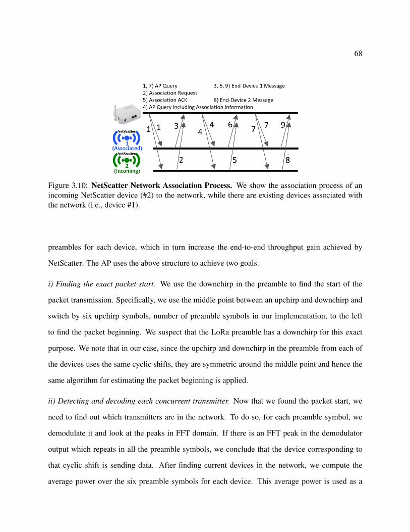
68
Figure 3.10: NetScatter Network Association Process. We show the association process of anincoming NetScatter device (#2) to the network, while there are existing devices associated withthe network (i.e., device #1).
preambles for each device, which in turn increase the end-to-end throughput gain achieved by
NetScatter. The AP uses the above structure to achieve two goals.
i) Finding the exact packet start. We use the downchirp in the preamble to find the start of the
packet transmission. Specifically, we use the middle point between an upchirp and downchirp and
switch by six upchirp symbols, number of preamble symbols in our implementation, to the left
to find the packet beginning. We suspect that the LoRa preamble has a downchirp for this exact
purpose. We note that in our case, since the upchirp and downchirp in the preamble from each of
the devices uses the same cyclic shifts, they are symmetric around the middle point and hence the
same algorithm for estimating the packet beginning is applied.
ii) Detecting and decoding each concurrent transmitter. Now that we found the packet start, we
need to find out which transmitters are in the network. To do so, for each preamble symbol, we
demodulate it and look at the peaks in FFT domain. If there is an FFT peak in the demodulator
output which repeats in all the preamble symbols, we conclude that the device corresponding to
that cyclic shift is sending data. After finding current devices in the network, we compute the
average power over the six preamble symbols for each device. This average power is used as a
69
threshold to demodulate the payload of each device. In particular, if the power of the device’s FFT
peak for each payload symbol is more than half this average, we interpret that as 1 and 0 otherwise.
3.4.2 Network Association
Say the network already has N devices associated to the AP and the N+1th device wants to join the
network. A naıve approach is to periodically dedicate time periods for association. This however
can lead to high association delays depending on the frequency of the association periods. Our
approach instead is to reserve Nassoc cyclic shifts and the corresponding FFT bins for association
and use the rest for communication. In other words, all the devices transmit at the same time but
the ones who want to enter the network transmit with the Nassoc association cyclic shifts.
To address the near-far problem, we reserve two cyclic shifts, one in high-SNR and the other
one in the low-SNR cyclic shift regions. The incoming device would choose which association
region to transmit based on the signal strength of the AP’s query message, calculated using the
envelope detector. However to account for the hardware delay variations, as before, we skip two
cyclic shifts to ensure that the association packets from the devices can be decoded and will not
interfere with communication cyclic shifts. Finally, to support scenarios where more than one
device want to associate at the same time, one can use Aloha protocol with binary exponential
back-off in the association process. Our deployment does not implement this option and turns ON
the backscatter devices one at a time and runs the network only after all the devices are associated.
After the incoming device sends its packet to the AP in association process using the association
cyclic shifts, the AP computes its signal strength and decides which cyclic shift and timing schedule
it should be assigned to. The AP piggybacks these assignments in its query messages.
3.4.3 AP Query Message
Fig. 3.11 shows the ASK-modulated query message that the AP sends. The message has a group ID
which identifies the set of 256 devices that should concurrently transmit. In our implementation,

70
Figure 3.11: Structure of AP’s Query Message.
since there are only 256 devices, we set this group ID to 0. In a larger network, the AP can assign
different sets of devices to different groups depending on their signal strengths, i.e., devices that
have a similar signal strength are grouped into the same group to enable concurrent transmissions
while further minimizing the near-far problem.
This is then followed by an optional association response payload that assigns an 8-bit network
ID and a 8-bit cyclic shift. Note that prior LoRa backscatter designs are request-response systems
that query each backscatter device sequentially and need most of the fields in Fig. 3.11 other
than the group ID and cyclic shift assignment. Since these additional 12 bits is transmitted using
160 kbps ASK downlink, the overhead is negligible compared to the 1 kbps backscatter uplink.
Finally, we note that if the AP is unable to assign a new device given the existing assignments, the
AP updates the cyclic shift assignments for all the devices in the network. It does so by transmitting
the identifier for one of the the 256! orderings, which requires log2(256!) (≤1700) bits. This
occupies less than 11 ms using our 160 kbps downlink.
3.4.4 Network Protocol
Fig. 3.10 summarizes our network protocol. First the AP broadcasts its query. Device 1, which
is already associated to the network receives the query and sends its data using its assigned cyclic
shift after performing any necessary power control. Concurrently, device 2 sends a Association
Request using one of the Nassoc cyclic shifts. The AP receives these two messages and broadcast
another query which includes association information for device 2. Upon receiving this query,
Device 1 continues to send its data, however, device 2 extract cyclic shift assignment from the
query and then transmits Association ACK to the AP in the assigned cyclic shift. If AP receives
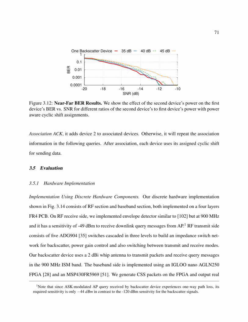
71
0.0001
0.001
0.01
0.1
1
-20 -18 -16 -14 -12 -10
BE
R
SNR (dB)
One Backscatter Device 35 dB 40 dB 45 dB
Figure 3.12: Near-Far BER Results. We show the effect of the second device’s power on the firstdevice’s BER vs. SNR for different ratios of the second device’s to first device’s power with poweraware cyclic shift assignments.
Association ACK, it adds device 2 to associated devices. Otherwise, it will repeat the association
information in the following queries. After association, each device uses its assigned cyclic shift
for sending data.
3.5 Evaluation
3.5.1 Hardware Implementation
Implementation Using Discrete Hardware Components. Our discrete hardware implementation
shown in Fig. 3.14 consists of RF section and baseband section, both implemented on a four layers
FR4 PCB. On RF receive side, we implemented envelope detector similar to [102] but at 900 MHz
and it has a sensitivity of -49 dBm to receive downlink query messages from AP.1 RF transmit side
consists of five ADG904 [35] switches cascaded in three levels to build an impedance switch net-
work for backscatter, power gain control and also switching between transmit and receive modes.
Our backscatter device uses a 2 dBi whip antenna to transmit packets and receive query messages
in the 900 MHz ISM band. The baseband side is implemented using an IGLOO nano AGLN250
FPGA [28] and an MSP430FR5969 [51]. We generate CSS packets on the FPGA and output real
1Note that since ASK-modulated AP query received by backscatter device experiences one-way path loss, itsrequired sensitivity is only −44 dBm in contrast to the -120 dBm sensitvity for the backscatter signals.

72
0
0.2
0.4
0.6
0.8
1
-150 -75 0 75 150
CD
F
Frequency (Hz)
(a) Frequency Offset
10-3
10-2
10-1
100
0 0.5 1 1.5 2
1-C
DF
∆FFTBin
BW=500 kHz,SF=9BW=250 kHz,SF=8
BW=125 kHz,SF=7
(b) FFT Bin Variation
Figure 3.13: Frequency Offset FFT Bin Variation. (a) frequency offset of backscatter devices,and (b) effect of residual time and frequency offset for different configurations.
and imaginary components of the square wave signal to the backscatter switch network. The en-
velope detector is controlled by the MCU. Downlink receiver algorithm is implemented on MCU.
To be resilient to self-interference caused by the AP’s single-tone, the baseband at the backscatter
device shifts the AP’s signal by 3 MHz. Note that the discrete implementation is for prototyp-
ing and proof-of-concept; an ASIC is typically required to achieve the orders of magnitude power
benefits of backscatter communication. We use a battery to power each backscatter device for our
evaluations.
IC Simulation. We design and simulate an IC for our backscatter device using TSMC 65nm LP
process. It consists of four blocks with total power consumption of 45.2 µW : i) An envelope de-
tector that demodulates the APs ASK query messages and consumes less than 1 µW . ii) Baseband
processor for processing and extracting AP data from envelope detector, interfacing with sensors
and sending the chirp specifications and sequence of data to chirp generator consuming 5.7 µW of
power. iii) A chirp generator that takes SF, BW, cyclic shift assignment and data sequence from
the baseband processor to generate the sequence of ON-OFF keying chirps. We use Verilog code
to describe the baseband signal’s phase behavior and generate assigned cyclic-shift with required
frequency offset. We use Synthesis, Auto-Place and Route (SAPR) to simulate Verliog code on
chip. The power consumption of this block is 36 µW . iv) We simulate a Switch network includ-
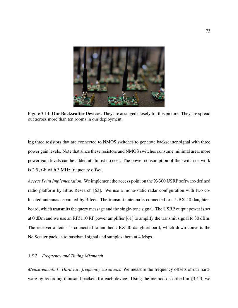
73
Figure 3.14: Our Backscatter Devices. They are arranged closely for this picture. They are spreadout across more than ten rooms in our deployment.
ing three resistors that are connected to NMOS switches to generate backscatter signal with three
power gain levels. Note that since these resistors and NMOS switches consume minimal area, more
power gain levels can be added at almost no cost. The power consumption of the switch network
is 2.5 µW with 3 MHz frequency offset.
Access Point Implementation. We implement the access point on the X-300 USRP software-defined
radio platform by Ettus Research [63]. We use a mono-static radar configuration with two co-
located antennas separated by 3 feet. The transmit antenna is connected to a UBX-40 daughter-
board, which transmits the query message and the single-tone signal. The USRP output power is set
at 0 dBm and we use an RF5110 RF power amplifier [61] to amplify the transmit signal to 30 dBm.
The receiver antenna is connected to another UBX-40 daughterboard, which down-converts the
NetScatter packets to baseband signal and samples them at 4 Msps.
3.5.2 Frequency and Timing Mismatch
Measurements 1: Hardware frequency variations. We measure the frequency offsets of our hard-
ware by recording thousand packets for each device. Using the method described in §3.4.3, we
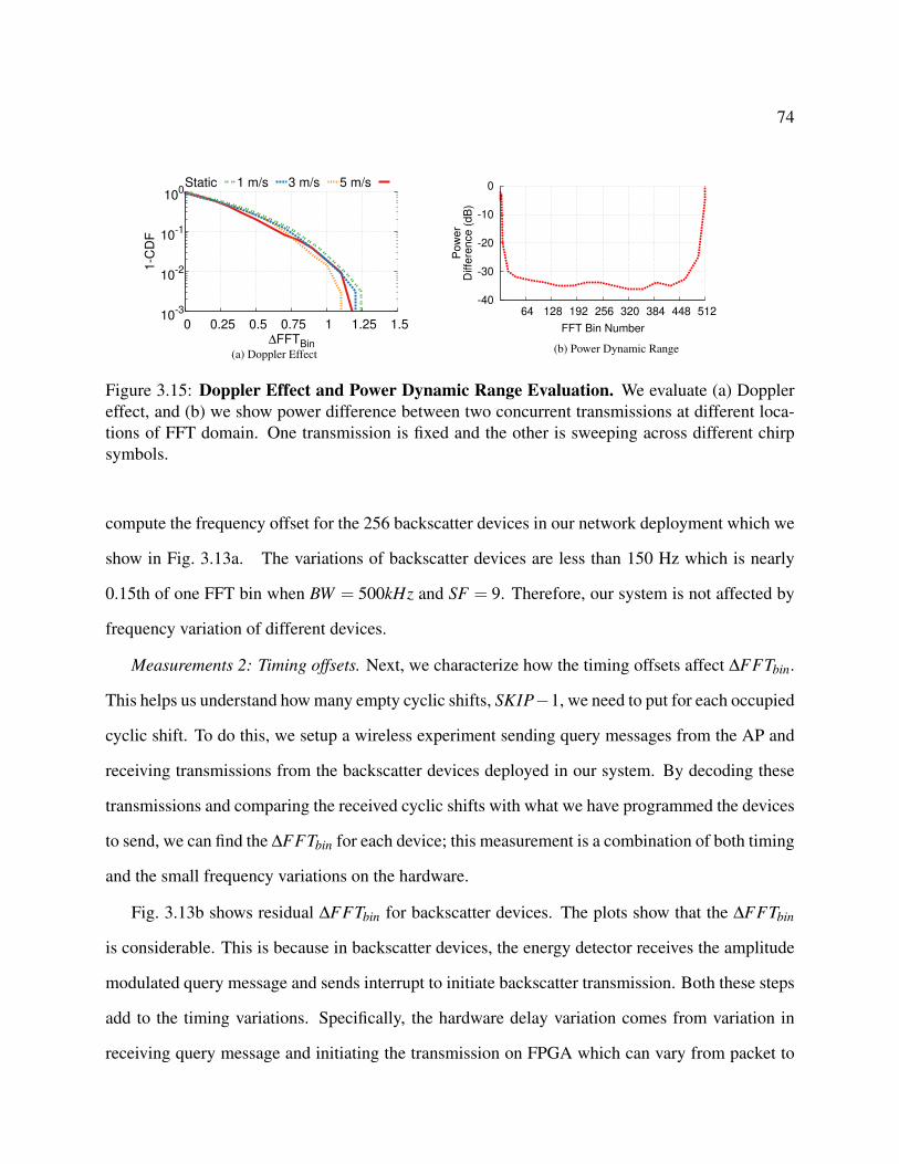
74
10-3
10-2
10-1
100
0 0.25 0.5 0.75 1 1.25 1.5
1-C
DF
∆FFTBin
5 m/s3 m/s1 m/sStatic
(a) Doppler Effect
-40
-30
-20
-10
0
64 128 192 256 320 384 448 512
Po
we
rD
iffe
ren
ce
(d
B)
FFT Bin Number
(b) Power Dynamic Range
Figure 3.15: Doppler Effect and Power Dynamic Range Evaluation. We evaluate (a) Dopplereffect, and (b) we show power difference between two concurrent transmissions at different loca-tions of FFT domain. One transmission is fixed and the other is sweeping across different chirpsymbols.
compute the frequency offset for the 256 backscatter devices in our network deployment which we
show in Fig. 3.13a. The variations of backscatter devices are less than 150 Hz which is nearly
0.15th of one FFT bin when BW = 500kHz and SF = 9. Therefore, our system is not affected by
frequency variation of different devices.
Measurements 2: Timing offsets. Next, we characterize how the timing offsets affect ∆FFTbin.
This helps us understand how many empty cyclic shifts, SKIP−1, we need to put for each occupied
cyclic shift. To do this, we setup a wireless experiment sending query messages from the AP and
receiving transmissions from the backscatter devices deployed in our system. By decoding these
transmissions and comparing the received cyclic shifts with what we have programmed the devices
to send, we can find the ∆FFTbin for each device; this measurement is a combination of both timing
and the small frequency variations on the hardware.
Fig. 3.13b shows residual ∆FFTbin for backscatter devices. The plots show that the ∆FFTbin
is considerable. This is because in backscatter devices, the energy detector receives the amplitude
modulated query message and sends interrupt to initiate backscatter transmission. Both these steps
add to the timing variations. Specifically, the hardware delay variation comes from variation in
receiving query message and initiating the transmission on FPGA which can vary from packet to
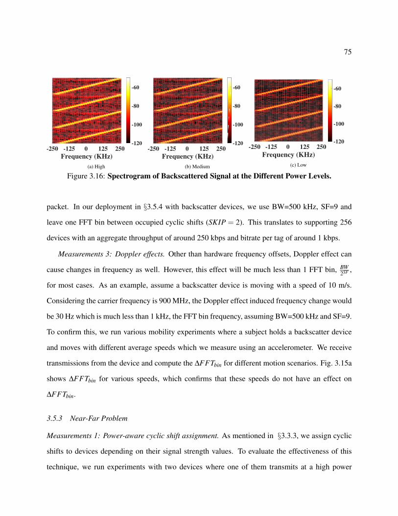
75
-250 -125 0 125 250
Frequency (KHz)
-120
-100
-80
-60
(a) High
-250 -125 0 125 250
Frequency (KHz)
-120
-100
-80
-60
(b) Medium
-250 -125 0 125 250
Frequency (KHz)
-120
-100
-80
-60
(c) Low
Figure 3.16: Spectrogram of Backscattered Signal at the Different Power Levels.
packet. In our deployment in §3.5.4 with backscatter devices, we use BW=500 kHz, SF=9 and
leave one FFT bin between occupied cyclic shifts (SKIP = 2). This translates to supporting 256
devices with an aggregate throughput of around 250 kbps and bitrate per tag of around 1 kbps.
Measurements 3: Doppler effects. Other than hardware frequency offsets, Doppler effect can
cause changes in frequency as well. However, this effect will be much less than 1 FFT bin, BW2SF ,
for most cases. As an example, assume a backscatter device is moving with a speed of 10 m/s.
Considering the carrier frequency is 900 MHz, the Doppler effect induced frequency change would
be 30 Hz which is much less than 1 kHz, the FFT bin frequency, assuming BW=500 kHz and SF=9.
To confirm this, we run various mobility experiments where a subject holds a backscatter device
and moves with different average speeds which we measure using an accelerometer. We receive
transmissions from the device and compute the ∆FFTbin for different motion scenarios. Fig. 3.15a
shows ∆FFTbin for various speeds, which confirms that these speeds do not have an effect on
∆FFTbin.
3.5.3 Near-Far Problem
Measurements 1: Power-aware cyclic shift assignment. As mentioned in §3.3.3, we assign cyclic
shifts to devices depending on their signal strength values. To evaluate the effectiveness of this
technique, we run experiments with two devices where one of them transmits at a high power
76
(equivalent to being near the AP) with a cyclic shift corresponding to the beginning of the FFT
spectrum. Then, we sweep the cyclic shift of the second device from small FFT bin difference
cyclic shifts to high FFT bin difference ones. At each cyclic shift, we decrease the power of
the second device using an attenuator up to when it has packet error rates less than one percent.
Fig. 3.15b shows the maximum power difference that can be tolerated between these two devices
versus the assigned FFT bin difference. As can be seen, as we go further in FFT bin difference,
we can tolerate more power difference between the two devices. Note that, because of aliasing
Fig. 3.15b is symmetric around the center. The maximum happens in middle and is equal to 35 dB.
This is the dynamic range that our system can support in practice. We also note that when the
second device is assigned to an FFT bin 2 cyclic shifts away from the first device, it can be up to
5 dB below the latter and still correctly decoded. This means there is an in-built 5 dB dynamic
range resilience to channel variations between devices that have close cyclic shifts.
Measurements 2: Self-aware power-adjustment. The second method to address the near-far
problem and also increase the dynamic-range is power adjustments at the devices using the signal
strength of the AP’s query message. To evaluate this, we first measure how well we can adjust
power on the devices. We evaluate its efficacy in practical deployments. We use three different
backscatter impedance values to be able to transmit packets in three different power gains. Fig. 3.16
shows the spectrum of backscattered signal at different power levels. These plots show that the
hardware creates spectrum that is clean and does not introduce noticeable non-linearities into the
backscattered signal. Furthermore, we can achieve three different power levels: 0, -4, and -10 dB.
3.5.4 Network Deployment
We evaluate three key network parameters:
• Network PHY bitrate. This is the bitrate achieved across all the devices during the payload
part of the packet.

77
0
50
100
150
200
250
1 16 32 64 96 128 160 192 224 256
Ph
ysic
al L
aye
rD
ata
Ra
te (
kb
ps)
# of Backscatter Devices
LoRa Backscatter without Rate Adaptation
LoRa Backscatter with Rate Adaptation
NetScatter (Ideal)
NetScatter
Figure 3.17: Network Physical Rate. We evaluate NetScatter network physical rate and compareit with other schemes.
• Link-layer data rate. This is the data rate achieved in the network which is defined as the data
rate for sending useful payload bits, after considering overheads including the AP’s query
message and the preamble of the packet transmission.
• Network latency. This is the latency to get the payload bits from all the backscatter devices
in the network.
We compare three schemes: i) LoRa backscatter [141] where all devices use a fixed bitrate of
8.7 kbps, ii) LoRa backscatter with rate adaptation where each device uses the best bitrate given its
channel conditions and iii) NetScatter. Note that the authors of [141] did not publicly release the
code and so, we replicate the implementation adding the missing details and using BW = 500 kHz
and SF = 9. We also note that [141] is not designed to work with more than one to two users. Here,
we use query-response design with scheduling when there are more users where the AP queries
each device. While LoRa backscatter does not support rate adaptation, we want to compare with
an ideal approach that maximizes the bitrate of each device by picking the optimal SF and BW . To
do so, we measure the signal strength from each of the backscatter devices and compute the bitrate
using the SNR table in [45]; this is the ideal performance a single-user LoRa backscatter design
achieves with rate adaptation.

78
Network PHY bitrate. We set each device bitrate to 976 bps, BWagg = 500 kHz, SF = 9 and a
payload size of five bytes. We deploy 256 backscatter devices across the floor of an office building
with more than ten rooms. Fig. 3.1 shows our deployment in an office. We hard-code cyclic
shift assignment on each device. Therefore, we skip the association phase in this deployment.
Fig. 3.17 shows the results of network physical rate for our backscatter network deployment. The
plot highlights the following key observations.
• The network data rate scales with the number of concurrent backscatter devices. When the
number of concurrent devices is less than 128, the variance in the throughput is small. This is
because in these scenarios effectively the backscatter devices are separated from each other
by more than 2 cyclic shifts (SKIP ≥ 3). As a result, the devices do not interfere with each
other and hence can concurrently operate. As we increase the concurrent devices to 256,
we are pushing the system to its theoretical limit (with SKIP = 2) and thus, we see larger
variances in the network data rate.
• With 256 backscatter devices, NetScatter increases the PHY bitrate by 6.8x and 26.2x over
LoRa backscatter with and without rate adaptation. The gains are lower with the ideal rate
adaptation since with rate adaptation high-SNR devices could pick the maximum LoRa bi-
trate of 32 kbps.
Link-layer data rate. While the above plots measure the data rate improvements for the message
payload, it does not account for the end-to-end overheads including preambles and the AP’s query
message to coordinate the concurrent transmissions. To see the effect of the AP query packet
overhead for NetScatter, we consider two configurations.
• NetScatter Config#1. In this scenario the cyclic shifts are all assigned during the association
phase and the AP query packet coordinating the concurrent transmissions is 32 bits long
without the optional fields in Fig. 3.11.
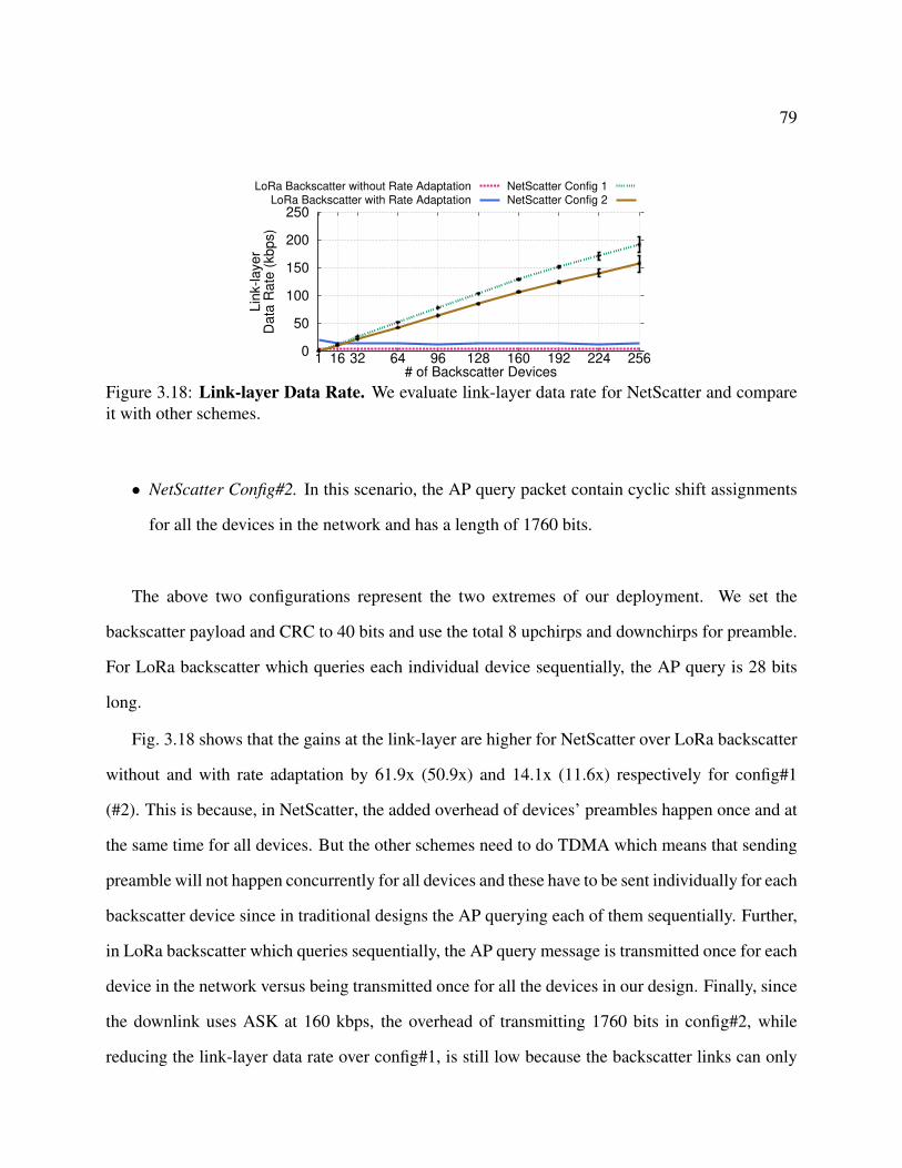
79
0
50
100
150
200
250
1 16 32 64 96 128 160 192 224 256
Lin
k-la
ye
rD
ata
Ra
te (
kb
ps)
# of Backscatter Devices
LoRa Backscatter without Rate Adaptation
LoRa Backscatter with Rate Adaptation
NetScatter Config 1
NetScatter Config 2
Figure 3.18: Link-layer Data Rate. We evaluate link-layer data rate for NetScatter and compareit with other schemes.
• NetScatter Config#2. In this scenario, the AP query packet contain cyclic shift assignments
for all the devices in the network and has a length of 1760 bits.
The above two configurations represent the two extremes of our deployment. We set the
backscatter payload and CRC to 40 bits and use the total 8 upchirps and downchirps for preamble.
For LoRa backscatter which queries each individual device sequentially, the AP query is 28 bits
long.
Fig. 3.18 shows that the gains at the link-layer are higher for NetScatter over LoRa backscatter
without and with rate adaptation by 61.9x (50.9x) and 14.1x (11.6x) respectively for config#1
(#2). This is because, in NetScatter, the added overhead of devices’ preambles happen once and at
the same time for all devices. But the other schemes need to do TDMA which means that sending
preamble will not happen concurrently for all devices and these have to be sent individually for each
backscatter device since in traditional designs the AP querying each of them sequentially. Further,
in LoRa backscatter which queries sequentially, the AP query message is transmitted once for each
device in the network versus being transmitted once for all the devices in our design. Finally, since
the downlink uses ASK at 160 kbps, the overhead of transmitting 1760 bits in config#2, while
reducing the link-layer data rate over config#1, is still low because the backscatter links can only

80
0
500
1000
1500
2000
2500
3000
3500
1 16 32 64 96 128 160 192 224 256
Ne
two
rk L
ate
ncy
(ms)
# of Backscatter Devices
LoRa Backscatter without Rate Adaptation
LoRa Backscatter with Rate Adaptation
NetScatter Config 1
NetScatter Config 2
Figure 3.19: Network Latency. We evaluate the latency of NetScatter and compare it with otherschemes. We define latency as total time for transmitting all the devices’ data.
achieve a much lower bitrate.
Network latency. Finally, Fig. 3.19 shows that NetScatter has a latency reduction of 67.0x
(55.1x) and 15.3x (12.6x) over prior LoRa backscatter without and with rate adaptation respectively
in network config#1 (#2). This is the key advantage of using concurrent transmissions in low-
power backscatter networks. It is noteworthy that since the downlink AP query bitrate is 160 kbps,
AP query duration is negligible compared to duration of backscatter devices’ preamble for prior
backscatter methods and also for config#1. For config#2, the AP query duration is significantly
higher than the config#1. However, the total duration is still dominated by the backscatter payload
+ CRC and preamble. As a result, AP query is not the dominant factor in link-layer latency.
3.6 Related Work
Recent systems use backscatter with Wi-Fi signals [102, 160], have a receiver sensitivity of only
-90 dBm and hence have a limited range and cannot work across rooms unless the RF source is
placed close to the backscatter tag [104, 102]. LoRa backscatter [141] can achieve long ranges
by generating LoRa-compliant chirp signals at the backscatter device. pLoRa [126] backscatters
ambient LoRa signals in the environment in contrast to the single tone used as the RF source in
NetScatter as well as [141]. We note that all SemTech LoRa chipsets have the capability in software
to transmit single tone signals. All these prior long range systems are evaluated in a network of

81
only 1–2 devices and propose to use time-division to support multiple backscatter devices. In
contrast, our design enables large-scale concurrent transmissions and can achieve much higher
link-layer data rates as well as lower latencies. We also note that these long range backscatter
systems [141, 126] claim a kilometer range in outdoor scenarios such as open fields. This however
requires placing the RF source close to the backscatter devices. In indoor environments where the
signal propagates through walls and the RF source is not placed close to the backscatter devices, our
network operational range across ten different rooms is consistent with these prior work. Finally,
we note that while prior work [141, 126] decodes the backscatter signal on Semtech LoRa chipsets,
our distributed CSS protocol is decoded on a software radio. We however note that SemTech LoRa
SX1257 [62] chipsets provide I-Q samples and hence our approach could also be implemented on
these off-the-shelf chipsets together with a low power FPGA for baseband processing; this however
is not in the scope of this work .
In addition, prior work [75, 147] use FMCW techniques to multiplex sources of FMCW re-
flectometry. Specifically, [75] uses FMCW to multiplex Fiber Bragg Grating (FBG) sensors at
different positions which results in different delays and different beat frequencies corresponding to
each sensor’s reflection. In contrast, NetScatter generates chirp signals with different cyclic-shifts
to modulate information on each backscatter device at the same time.
Finally, recent work on decoding concurrent transmissions from RFID tags, does not achieve
the long range operations and below-noise operations of CSS based systems. Buzz [150], LF-
Backscatter [91], and others [92, 122, 97] leverage the differences in the time domain signal tran-
sitions and changes in the constellation diagram to decode multiple RFIDs. However, the number
of concurrent transmissions in the above designs is limited — the latest in this line of work, Flip-
tracer [97], can reliably decode up to five concurrent RFID tags. Further, these systems were tested
with ranges of 0.5 to 6 feet [150, 91, 97] and in the same room. Finally, receiver sensitivity of
even battery-powered backscatter tags for RFID EPC-GEN2 readers is around -85 dBm. So it can-
82
not support the long ranges and whole-home deployments that CSS modulation based backscatter
achieves.
3.7 Conclusion
We present a new wireless protocol for backscatter networks that scales to hundreds of concurrent
transmissions. To this end, we introduce, distributed chirp spread spectrum coding, which uses a
combination of chirp spread spectrum (CSS) modulation and ON-OFF keying. Further, we address
practical issues including near-far problem and timing and frequency synchronization. Finally,
we deploy our system in an indoor environment with 256 concurrent devices to demonstrate its
throughput and latency performance.
83
Chapter 4
TINYSDR: LOW-POWER SDR PLATFORM FOR OVER-THE-AIRPROGRAMMABLE IOT TESTBEDS
Recent years have seen development of numerous wireless protocols for Internet of Things
(IoT) devices. In addition to longtime standards such as Bluetooth and Zigbee, a number of new
protocols including LoRa, Sigfox, NB-IoT and LTE-M have been developed that achieve long
ranges of more than a few kilometers. Due to the lack of a de-facto standard, this space remains an
active area of research for both industry and academia. The rapid advances in this space however
present practical challenges for researchers: each of these protocols requires a dedicated radio
chipset to evaluate, and these proprietary solutions often leave little room for protocol modification.
The academic community is therefore severely handicapped by the lack of a flexible platform, as
even a complex multi-radio prototype cannot adapt to evaluate new protocols or even customize
existing solutions. The current ecosystem therefore discourages researchers from investigating
the important questions that arise when scaling up IoT networks, and more importantly taking a
systematic approach to developing new protocols from the ground up.
Ideally, we would like a large scale IoT network testbed with the flexibility to run any IoT
protocol at the PHY and MAC layers. Further, since many of these IoT testbeds can span hundreds
of endpoints across a large campus or even a city, we need the ability to push changes to the PHY
and MAC layers, using simple over-the-air software updates. This would allow for performance
comparisons on a single testbed to investigate the trade-offs between existing standards as well as
showcase the advantages of an entirely new custom protocol. Moreover, to make such a system
representative of real-world deployments, individual network nodes should model the constraints

84
Figure 4.1: TinySDR Hardware Platform. It has two antenna ports for running IoT PHY and MAC protocols at2.4 GHz and 900 MHz. This image is the actual size of the platform on printed paper.
of IoT endpoints. Specifically, these devices should have appropriate power controls and options to
duty cycle transmissions, have an ultra-low power sleep mode and also have interfaces to connect
sensors. Finally, the ability to run these endpoints on batteries would also allow for flexibility of
deployment in spaces without dedicated power access, or even in mobile scenarios.
Realizing this vision however is challenging with existing software defined radio (SDR) plat-
forms. Specifically, we require an SDR for the flexibility of implementing different PHY proto-
cols; but there is currently no SDR platform that meets the requirements of IoT endpoints (see
Table 4.1). Existing SDR systems consume large amounts of power for transmitting data, do not
support ultra-low power sleep modes, require wired infrastructure and often a dedicated computer
and furthermore, are expensive. More importantly, none of the existing SDR platforms support
over-the-air programming to update PHY or MAC protocols. Finally, IoT devices prioritize power
consumption and communication range and hence use limited radio bandwidth — LoRa, Sigfox,
NB-IoT, LTE-M, Bluetooth and ZigBee use only 500 kHz, 200 Hz, 180 kHz, 1.4 MHz, 2 MHz
and 2 MHz respectively. In contrast, existing SDR platforms focus on achieving high performance
in terms of bandwidth because they are tailored to the needs of gateway devices and not for IoT
endpoint devices.
Driven by a need for such a platform in our own research, we design tinySDR as shown in
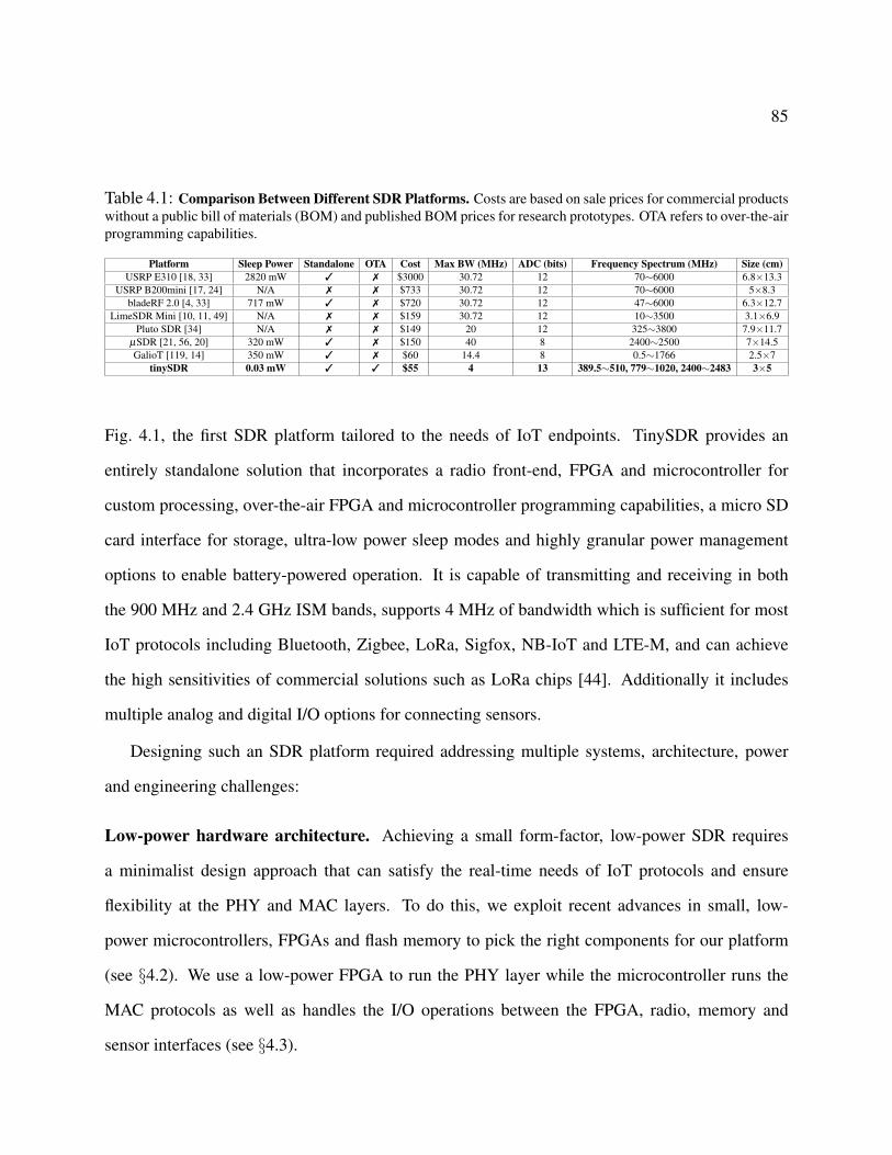
85
Table 4.1: Comparison Between Different SDR Platforms. Costs are based on sale prices for commercial productswithout a public bill of materials (BOM) and published BOM prices for research prototypes. OTA refers to over-the-airprogramming capabilities.
Platform Sleep Power Standalone OTA Cost Max BW (MHz) ADC (bits) Frequency Spectrum (MHz) Size (cm)USRP E310 [18, 33] 2820 mW 3 7 $3000 30.72 12 70∼6000 6.8×13.3
USRP B200mini [17, 24] N/A 7 7 $733 30.72 12 70∼6000 5×8.3bladeRF 2.0 [4, 33] 717 mW 3 7 $720 30.72 12 47∼6000 6.3×12.7
LimeSDR Mini [10, 11, 49] N/A 7 7 $159 30.72 12 10∼3500 3.1×6.9Pluto SDR [34] N/A 7 7 $149 20 12 325∼3800 7.9×11.7
µSDR [21, 56, 20] 320 mW 3 7 $150 40 8 2400∼2500 7×14.5GalioT [119, 14] 350 mW 3 7 $60 14.4 8 0.5∼1766 2.5×7
tinySDR 0.03 mW 3 3 $55 4 13 389.5∼510, 779∼1020, 2400∼2483 3×5
Fig. 4.1, the first SDR platform tailored to the needs of IoT endpoints. TinySDR provides an
entirely standalone solution that incorporates a radio front-end, FPGA and microcontroller for
custom processing, over-the-air FPGA and microcontroller programming capabilities, a micro SD
card interface for storage, ultra-low power sleep modes and highly granular power management
options to enable battery-powered operation. It is capable of transmitting and receiving in both
the 900 MHz and 2.4 GHz ISM bands, supports 4 MHz of bandwidth which is sufficient for most
IoT protocols including Bluetooth, Zigbee, LoRa, Sigfox, NB-IoT and LTE-M, and can achieve
the high sensitivities of commercial solutions such as LoRa chips [44]. Additionally it includes
multiple analog and digital I/O options for connecting sensors.
Designing such an SDR platform required addressing multiple systems, architecture, power
and engineering challenges:
Low-power hardware architecture. Achieving a small form-factor, low-power SDR requires
a minimalist design approach that can satisfy the real-time needs of IoT protocols and ensure
flexibility at the PHY and MAC layers. To do this, we exploit recent advances in small, low-
power microcontrollers, FPGAs and flash memory to pick the right components for our platform
(see §4.2). We use a low-power FPGA to run the PHY layer while the microcontroller runs the
MAC protocols as well as handles the I/O operations between the FPGA, radio, memory and
sensor interfaces (see §4.3).
86
Efficient power management. Achieving highly granular power management needed for battery-
powered operation and enabling ultra-low power sleep modes requires shutting down parts of SDR
when not in use. This is important for IoT endpoints that perform duty-cycled operations and
require an ultra-low power sleep mode to achieve a long battery life. This presents a design tradeoff
between the complexity of toggling the power of each hardware component ON and OFF, and the
cost of additional circuitry to do so. We address this challenge in §4.4 and achieve sleep power as
low as 30 µW.
Over-the-air SDR programming. Enabling a truly scalable system requires the ability to update
the PHY and MAC layers on the platform, over-the-air, in a testbed deployment. This however
also introduces the challenge of over-the-air FPGA and microcontroller programming as well as
communicating these updates robustly to each device in the network while minimizing power con-
sumption and network utilization. We use a dedicated wireless backbone subsystem complete with
a MAC protocol and its own flash memory to program both the microcontroller and FPGA. Addi-
tionally we leverage compression and low-power decompression algorithms to minimize network
downtime during the updates (see §4.5)
Fig. 4.2 shows the power consumption of the radio module in tinySDR compared to existing
SDR platforms. We evaluate tinySDR’s performance by presenting case studies of two common
protocols: LoRa and BLE beacons, and also evaluate tinySDR in a campus-testbed of 20 devices.
LoRa modulation and demodulation use 4% and 11% of the FPGA resources respectively and
achieve a sensitivity of -126 dBm for 3.12 kbps, which is similar to an SX1276 [44] LoRa chip
with the same configuration. Further, the FPGA supports real-time modulation and demodulation
of all LoRa spreading factors from 6 to 12. A LoRa MAC implementation on our MCU is also
compatible with the The Things Network.
TinySDR supports 2.4 GHz BLE beacon transmissions. The full baseband packet generation on
the FPGA uses 3% of its resources. The platform can perform frequency hopping with a delay

87
of 220 us and achieves a sensitivity of -94 dBm which is comparable to the commercial BLE
chipsets [37].
Finally, we present a case study of how the unique capabilities of tinySDR could be used
to answer new research questions. Recent work has explored techniques to enable concurrent
transmissions in LoRa networks [83, 89]; however these solutions were prototyped on USRPs and
it is unclear if IoT endpoints can decode concurrent transmissions in real-time within their power
and resource constraints. We implement a custom decoder on tinySDR to demonstrate for the first
time that IoT endpoints can receive concurrent transmissions.
Contributions. To summarize, we design the first SDR platform tailored to the needs of IoT
endpoint devices. By making careful design and architectural choices, our platform achieves low
power, supports IoT protocols at both 900 MHz and 2.4 GHz and has computation resources to
do on-board processing. We present a highly granular power management scheme that enables
duty-cycled operation and 10,000x lower power sleep modes. We also develop the first over-the-
air SDR programming capability to support PHY and MAC updates in a wireless testbed. We
characterize and evaluate our platform with case studies of LoRa and BLE beacons. Finally, we
present a research exploration of concurrently receiving multiple LoRa transmissions on our SDR
platform.
Platform availability. TinySDR’s hardware schematics and software are available at:
https://github.com/uw-x/tinysdr
4.1 SDR Requirements for IoT Nodes
To motivate the need for LoRa backscatterand inform our design decisions, we begin by identifying
the key requirements for an IoT endpoint. These include 1) operation in the 900 MHz and 2.4 GHz
bands, 2) low power operation which requires the ability to transition to ultra-low power sleep
mode, 3) standalone operation which requires an on-board control unit to duty cycle the radio, 4)
88
over-the-air programming capabilities for large scale IoT testbeds, 5) low cost per node, and 6)
at least 2 MHz bandwidth to support IoT protocols including LoRa, SIGFOX, LTE-M, NB-IoT,
ZigBee and Bluetooth. While there are a number of commercially available SDRs such as the
USRP, BladeRF, Pluto SDR, and LimeSDR [18, 4, 63, 11, 57] on the market and SDR research
prototypes such as WARP, Argos, SORA, SODA, KUAR, Tick, µSDR, OpenMili, and GalioT [68,
103, 69, 143, 87, 119, 105, 106, 82, 158, 110, 153, 114, 140, 121, 137, 136], all of them are
designed as gateway devices and do not satisfy many of the above constraints. Here, we analyze
the shortcomings of these platforms in the context of these requirements.
Low power operation and sleep mode. Fig. 4.2 compares the power consumption of the radio
module alone in existing SDR platforms, since each one has different peripherals. We find that
most SDR platforms consume 200-300 mW in receive mode, but a lot more power when transmit-
ting. While this may be acceptable for a gateway devices that are more often receiving, typical IoT
endpoints do the opposite and are required to transmit data like sensor information. Moreover, real
IoT nodes spend a very short time transmitting before transitioning to ultra-low power sleep modes.
Although IoT radios often consume tens to hundreds of milliwatts of power, the key to achieving
long battery lifetimes is exploiting their microwatt power sleep modes. Table 4.1 shows that none
of the other platforms can benefit from duty cycling as they consume more power in sleep mode
than LoRa backscatterdoes when transmitting; LoRa backscatter’s microwatt power consumption
in sleep mode enables dramatic power savings with duty cycling.
Standalone operation and cost. We observe that some of these platforms do not allow for stan-
dalone operation, i.e., they cannot be used in a testbed deployment without an external computer.
Among the ones that do, the Embedded USRP and bladeRF cost $700 or more per unit making
large scale deployments expensive. µSDR allows for standalone operation but only operates at
2.4 GHz and cannot support protocols like LoRa. GalioT [119] uses the low cost RTL2832U ra-
dio [14] connected to a Raspberry Pi computer which allows for standalone operation, however it

89
0
0.3
0.6
0.9
1.2
1.5
UBX 4
0
USR
P E31
0
USR
P B20
0
blad
eRF 2
.0
Lim
eSDR
Mini
Pluto
SDR
uSDR
GalioT
TinyS
DR
Po
we
rC
on
su
mp
tio
n (
W)
TX RX14dBm
10dBm 10dBm 10dBm10dBm10dBm 14dBm
No TX
14dBm
Figure 4.2: Radio Module Power Consumption for Each Platform. The TX output power ofeach radio module is shown on top of it.
does not support 2.4 GHz band. Moreover, this platform is receiver only and cannot be used to
prototype a typical IoT node that transmits data.
Over-the-air (OTA) programming. As shown in Table 4.1, all existing SDR platforms rely on
wired interfaces for programming. This means that even if one of these systems were connected
to a battery, running an experiment would require either tethering each one to a wired network or
individually programming them. An OTA programming system is crucial to realizing the goal of a
large scale wide area testbed as without it, researchers have to decide between limiting themselves
to deployment scenarios with wired infrastructure that are not representative of real IoT use cases or
traveling over kilometer distances to update individual nodes for each minor protocol modification,
which would be unmanageable at scale.
4.2 TinySDR Platform
We first describe our design choices for the different components of our hardware shown in Fig. 4.3
and explain the interfaces between them. Next we present the power management module which
enables our ultra-low-power sleep mode. Finally, we describe our over-the-air update protocol
including decompression algorithms and over-the-air reprogramming.
We seek to minimize power consumption and cost while offering the flexibility of an SDR to

90
process raw samples.
4.2.1 Designing the Software Radio
The core block on our platform is the software-defined radio, a programmable PHY layer that
processes and converts bits to radio signals and vice versa. We begin by explaining our choices for
the primary components of an SDR which are a radio chip that provides an interface for sending
and receiving raw samples of an RF signal as well as an FPGA that can process these signals in
real time. We then discuss the supporting peripherals for these devices such as a power amplifier
(PA) to boost the output of the radio chip and non-volatile memory for the FPGA to read and write
data from.
Choosing a radio chip. We begin by choosing a radio chip as its specs define the requirements
for the FPGA and other blocks. Our primary requirement is that the chip supports reading and
writing raw complex I/Q samples of the RF signal. As shown in Table 4.2, current SDR systems
use I/Q radio chips that are designed to cover a multi-GHz spectrum and have high ADC/DAC
sampling rates to support large bandwidth. For example, the AD936x [33] series which is used in
USRP and Pluto SDR can transmit up to 3.8 GHz and supports sampling rates as high as tens of
MHz. Each of these specs such as wide bandwidth, low noise, and high sampling rate represent
fundamental trade offs of power for performance, and therefore these chips consume watts of
power. Moreover, some of these radio chips costs more than $100.
We instead take a different approach: identify the minimum required specs and find a radio that
supports them. Specifically, a radio chip for an IoT platform must be able to operate in at least
the 900 MHz and 2.4 GHz ISM bands, have 4 MHz of bandwidth, while otherwise minimizing
power and ideally costing less than $10. We analyze all of the commercially available radio chips
that provide baseband I/Q samples and list them in Table 4.2, where only the AT86RF215 supports
all of our requirements. In addition to its lower cost and support for both frequency bands, it also
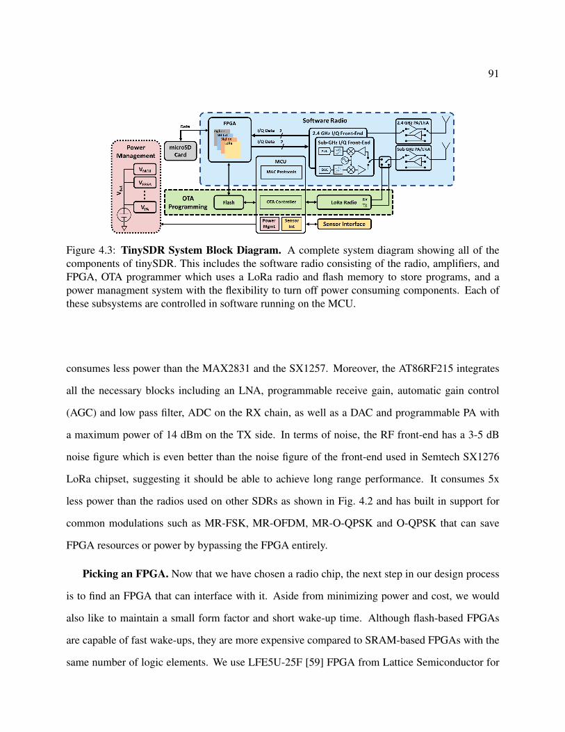
91
Figure 4.3: TinySDR System Block Diagram. A complete system diagram showing all of thecomponents of tinySDR. This includes the software radio consisting of the radio, amplifiers, andFPGA, OTA programmer which uses a LoRa radio and flash memory to store programs, and apower managment system with the flexibility to turn off power consuming components. Each ofthese subsystems are controlled in software running on the MCU.
consumes less power than the MAX2831 and the SX1257. Moreover, the AT86RF215 integrates
all the necessary blocks including an LNA, programmable receive gain, automatic gain control
(AGC) and low pass filter, ADC on the RX chain, as well as a DAC and programmable PA with
a maximum power of 14 dBm on the TX side. In terms of noise, the RF front-end has a 3-5 dB
noise figure which is even better than the noise figure of the front-end used in Semtech SX1276
LoRa chipset, suggesting it should be able to achieve long range performance. It consumes 5x
less power than the radios used on other SDRs as shown in Fig. 4.2 and has built in support for
common modulations such as MR-FSK, MR-OFDM, MR-O-QPSK and O-QPSK that can save
FPGA resources or power by bypassing the FPGA entirely.
Picking an FPGA. Now that we have chosen a radio chip, the next step in our design process
is to find an FPGA that can interface with it. Aside from minimizing power and cost, we would
also like to maintain a small form factor and short wake-up time. Although flash-based FPGAs
are capable of fast wake-ups, they are more expensive compared to SRAM-based FPGAs with the
same number of logic elements. We use LFE5U-25F [59] FPGA from Lattice Semiconductor for
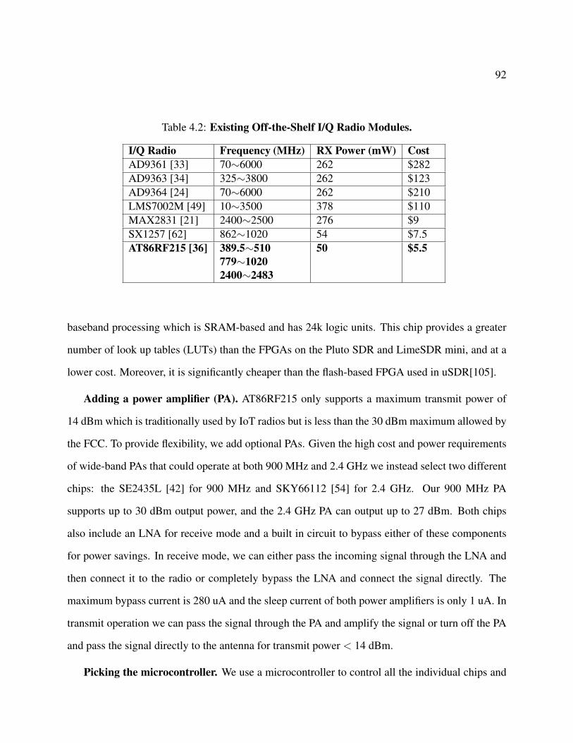
92
Table 4.2: Existing Off-the-Shelf I/Q Radio Modules.
I/Q Radio Frequency (MHz) RX Power (mW) CostAD9361 [33] 70∼6000 262 $282AD9363 [34] 325∼3800 262 $123AD9364 [24] 70∼6000 262 $210LMS7002M [49] 10∼3500 378 $110MAX2831 [21] 2400∼2500 276 $9SX1257 [62] 862∼1020 54 $7.5AT86RF215 [36] 389.5∼510
779∼10202400∼2483
50 $5.5
baseband processing which is SRAM-based and has 24k logic units. This chip provides a greater
number of look up tables (LUTs) than the FPGAs on the Pluto SDR and LimeSDR mini, and at a
lower cost. Moreover, it is significantly cheaper than the flash-based FPGA used in uSDR[105].
Adding a power amplifier (PA). AT86RF215 only supports a maximum transmit power of
14 dBm which is traditionally used by IoT radios but is less than the 30 dBm maximum allowed by
the FCC. To provide flexibility, we add optional PAs. Given the high cost and power requirements
of wide-band PAs that could operate at both 900 MHz and 2.4 GHz we instead select two different
chips: the SE2435L [42] for 900 MHz and SKY66112 [54] for 2.4 GHz. Our 900 MHz PA
supports up to 30 dBm output power, and the 2.4 GHz PA can output up to 27 dBm. Both chips
also include an LNA for receive mode and a built in circuit to bypass either of these components
for power savings. In receive mode, we can either pass the incoming signal through the LNA and
then connect it to the radio or completely bypass the LNA and connect the signal directly. The
maximum bypass current is 280 uA and the sleep current of both power amplifiers is only 1 uA. In
transmit operation we can pass the signal through the PA and amplify the signal or turn off the PA
and pass the signal directly to the antenna for transmit power < 14 dBm.
Picking the microcontroller. We use a microcontroller to control all the individual chips and
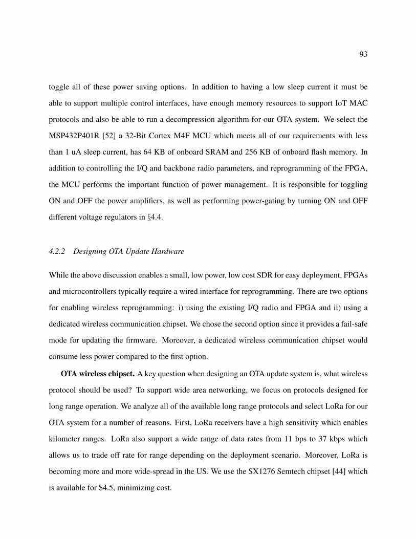
93
toggle all of these power saving options. In addition to having a low sleep current it must be
able to support multiple control interfaces, have enough memory resources to support IoT MAC
protocols and also be able to run a decompression algorithm for our OTA system. We select the
MSP432P401R [52] a 32-Bit Cortex M4F MCU which meets all of our requirements with less
than 1 uA sleep current, has 64 KB of onboard SRAM and 256 KB of onboard flash memory. In
addition to controlling the I/Q and backbone radio parameters, and reprogramming of the FPGA,
the MCU performs the important function of power management. It is responsible for toggling
ON and OFF the power amplifiers, as well as performing power-gating by turning ON and OFF
different voltage regulators in §4.4.
4.2.2 Designing OTA Update Hardware
While the above discussion enables a small, low power, low cost SDR for easy deployment, FPGAs
and microcontrollers typically require a wired interface for reprogramming. There are two options
for enabling wireless reprogramming: i) using the existing I/Q radio and FPGA and ii) using a
dedicated wireless communication chipset. We chose the second option since it provides a fail-safe
mode for updating the firmware. Moreover, a dedicated wireless communication chipset would
consume less power compared to the first option.
OTA wireless chipset. A key question when designing an OTA update system is, what wireless
protocol should be used? To support wide area networking, we focus on protocols designed for
long range operation. We analyze all of the available long range protocols and select LoRa for our
OTA system for a number of reasons. First, LoRa receivers have a high sensitivity which enables
kilometer ranges. LoRa also support a wide range of data rates from 11 bps to 37 kbps which
allows us to trade off rate for range depending on the deployment scenario. Moreover, LoRa is
becoming more and more wide-spread in the US. We use the SX1276 Semtech chipset [44] which
is available for $4.5, minimizing cost.
94
Figure 4.4: I/Q Word Structure Used by I/Q Radio.
Flash Memory. Our FPGA is SRAM based and does not include on-chip non-volatile memory
for storing programming data. We instead store the firmware bitstream on a separate flash memory
chip. The FPGA programming bitstream is 579 KB and the MCU programs require a maximum of
256 KB. We chose the MX25R6435F flash chip with 8 MB memory. Although this is far more than
the size required, it allows LoRa backscatterto store multiple FPGA bitstreams and MCU programs
to quickly switch between stored protocols without having to re-send the programming data over
the air.
4.3 Interfacing Between Blocks
4.3.1 Reading and Writing I/Q Samples
The AT86RF215 radio chipset samples baseband signals at 4 MHz with a 13 bit resolution for both
I and Q. Operating at the full rate therefore requires an interface which can support a throughput of
over 100 Mbps without consuming a large amount of power to meet our design objectives. To do
this we use low-voltage differential signaling (LVDS) [13] which is a high-speed digital interface
that reduces power by using lower voltage signals but maintains good SNR by sending data over
two differential lines to reduce common mode noise.
Receiving serial I/Q data. Our system communicates over LVDS to the FPGA in serial mode
to transfer I/Q data with a physical interface consisting of 4 I/O lines, pairs of which are used to
send data and clock signals. The radio outputs 32-bit serial data words at 4 Mwords/s using the
format in Fig. 4.4. Each data word starts with the I SY NC pattern which indicates the start of the
I sample which we use for synchronization. Next, it has 13 bits of I Data followed by a control

95
bit. The same format follows for Q, beginning with a synchronization pattern Q SY NC and then
13 bits for Q Data and the final control bit. The required 128 Mbps data rate is achieved using a
64 MHz clock provided by the radio operating at double data rate by sampling at both the rising
and falling edges of the clock. We implement an I/Q deserializer on the FPGA to read the data
which samples the input at both the rising and falling edges of the clock, uses the I SY NC and
Q SY NC to detect the beginning of the data fields and loads the I and Q values into 13 bit registers
for parallel processing.
Transmitting I/Q samples. In TX mode we need to do the opposite of the above sequence
to convert from the parallel representation on the FPGA to a serialized LVDS stream. To do this,
we use the FPGA’s onboard PLL to generate the 64 MHz clock signal. Next to create our double
data rate output signal that varies on both the positive and negative edges of this clock signal using
a dual-edge D flip-flop design [90] resulting in the desired 128 Mbps data rate. We use this to
generate the same I/Q word structure described above.
4.3.2 Memory Interfaces
After reading the raw data from the LVDS lines using the I/Q deserializer described above, we store
the samples into a FIFO buffer implemented using the FPGA’s embedded SRAM. We implement
a simple memory controller to write data to the FIFO which generates the memory control signals
and writes a full data word on each cycle. The embedded memory can run at rates significantly
greater than 4 MHz meaning it is not a limiting factor for real-time processing. The SRAM can
buffer up to 126 kB. The data stored in the FIFO can then be sent to signal processing blocks to
implement filters, cryptographic functions, etc. or to non-volatile flash memory. For flash memory,
we use a micro SD card which enables us to collect raw I/Q data and analyze the spectrum. The
micro SD card supports two modes: native SD mode and standard SPI mode. In native SD mode,
micro SD card’s interface uses 4 parallel data lines to read/write data to/from the micro SD card.
96
This mode supports a higher data rate compared to the SPI mode which only supports a 1-bit serial
interface. However, we implement SPI mode since it supports the 104 Mbps data rate which we
need to write data in real time. This allows us to re-use the same, simpler SPI block for multiple
functions and save resources on the FPGA.
4.3.3 RF, Control and Sensor Interfaces
The AT86RF215 provides differential RF signals for both 900 MHz and 2.4 GHz and has an inte-
grated TX/RX switch for both. At 2.4 GHz, the differential signal is transformed to a single-ended
output using the 2450FB15A050E [19] balun and fed to the SKY66112 [54] front-end with the
bypassable LNA and PA. Finally, after passing through a matching network, the 2.4 GHz signal is
connected to an SMA output.
On the 900 MHz side, the differential output of the AT86RF215 is connected to 0896BM15E0025E [58]
to convert it to a single-ended output. This must be shared between the backbone radio’s two sepa-
rate RF paths for transmit and receive and AT86RF215’s 900 MHz single-ended signal. We choose
between them using a ADG904 [35] SP4T RF switch. The single port side is connected to the
SE2435L [42] 900 MHz front-end which is similar to the 2.4 GHz front-end. The MCU commu-
nicates with the I/Q radio, backbone radio, FPGA and Flash memory through SPI which it uses to
send commands for changing the frequency, selecting the outputs, etc. It also has control signals
for FPGA programming, 900 MHz and 2.4 GHz front-end modules, RF switch and voltage regu-
lators for active power control. TinySDR supports common digital interfaces like SPI and I2C to
communicate with digital sensors and two analog to digital converters (ADC) for interfacing with
analog sensors. We leverage the internal flash memory of the MCU (≈ 256 kB) and external flash
memory (≈ 8 MB) to store sensor data.

97
Table 4.3: Power Domains in TinySDR.
Component Voltage [V] Power DomainMCU 1.8 V1FPGA 1.1, 1.8, 2.5, Vlvds V2, V3, V4, V5
I/Q Radio 1.8 < V5 < 3.6 V5Backbone Radio 1.8 < V5 < 3.6 V5
sub-GHz PA 3.5 V62.4 GHz PA 1.8, 3.0 V3, V7
FLASH Memory 1.8 V3Micro SD Memory 3.0 V7
4.4 Power Management Unit
Next, we present the design of our power management unit which seeks to maximize the system
lifetime when running off of a 3.7 V Lithium battery. To enable long battery lifetimes we need
to be able to duty-cycle our system and allow the MCU to toggle each of the above blocks ON
and OFF when they are not in use. Further, different components have different supply voltage
requirements and we wish to provide each one with the lowest voltage possible to minimize power
usage.
Ideally we would want separate controllable voltage regulators for each component in the sys-
tem. However, having many different regulators with individual controls significantly increases
the complexity, number of components, and price. Moreover, it complicates the PCB design by
requiring many control signals and a multitude of power planes. Therefore, there exists a trade-off
between the granularity of power control and the price/complexity of a design. We outline the sup-
ply voltages needed for each component and the power domain supporting it in Table 4.3. Below,
we show how we group components to balance power and complexity.
• Power domain V1 (MCU). Since the MCU is the central controller that implements power
management, it needs to be powered at all times and therefore has its own power domain. To

98
minimize its sleep current we need to use a voltage regulator with a low quiescent current.
Although switching voltage regulators have higher conversion efficiency when active, they
also have high quiescent currents so we instead select the TPS78218 linear regulator.
• Power domains V2, V3, V4, V6 and V7. These power domains provide power to blocks
such as the FPGA, memory blocks, and PAs. Since these components can all be turned off
when not operating, the voltage regulators for these domains should have low shut-down
current during sleep and high efficiency when active. We therefore choose the TPS62240
which has a shutdown current of only 0.1 uA. It is highly efficient and is rated to support
the current draw required by all components except the 900 MHz PA. To support this PA
at its maximum output power we use the TPS62080 switching regulator which supports the
required current.
• Power domain V5. V5 is a shared power domain for I/Q radio, backbone LoRa radio and
FPGA I/O bank. This power domain is initially set to 1.8V to minimize power consumption,
however components such as the radio chips can require higher voltage to achieve maximum
output power. Therefore, in addition to high efficiency and low shut-down current like the
others, this domain should be programmable. To do this, we use Semtech SC195ULTRT [27]
which provides an adjustable output that can be set from 1.8 V to 3.6 V.
4.5 Over-the-Air Programming protocol
OTA AP and MAC protocol. To update a network of tinySDR devices, we use an AP with a LoRa
radio to communicate with each device sequentially. In order to propagate updates throughout a
testbed or to specific tinySDR nodes, we design a MAC layer for the LoRa PHY. We pre-program
a timer on the MCU to periodically turn off the FPGA and switch from IQ radio mode to the back-
bone radio to listen for new firmware updates. If there is an update, the AP sends a programming
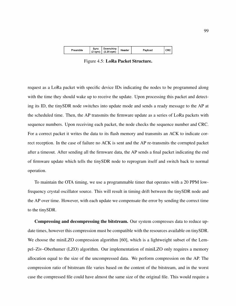
99
Figure 4.5: LoRa Packet Structure.
request as a LoRa packet with specific device IDs indicating the nodes to be programmed along
with the time they should wake up to receive the update. Upon processing this packet and detect-
ing its ID, the tinySDR node switches into update mode and sends a ready message to the AP at
the scheduled time. Then, the AP transmits the firmware update as a series of LoRa packets with
sequence numbers. Upon receiving each packet, the node checks the sequence number and CRC.
For a correct packet it writes the data to its flash memory and transmits an ACK to indicate cor-
rect reception. In the case of failure no ACK is sent and the AP re-transmits the corrupted packet
after a timeout. After sending all the firmware data, the AP sends a final packet indicating the end
of firmware update which tells the tinySDR node to reprogram itself and switch back to normal
operation.
To maintain the OTA timing, we use a programmable timer that operates with a 20 PPM low-
frequency crystal oscillator source. This will result in timing drift between the tinySDR node and
the AP over time. However, with each update we compensate the error by sending the correct time
to the tinySDR.
Compressing and decompressing the bitstream. Our system compresses data to reduce up-
date times, however this compression must be compatible with the resources available on tinySDR.
We choose the miniLZO compression algorithm [60], which is a lightweight subset of the Lem-
pel–Ziv–Oberhumer (LZO) algorithm. Our implementation of miniLZO only requires a memory
allocation equal to the size of the uncompressed data. We perform compression on the AP. The
compression ratio of bitstream file varies based on the content of the bitstream, and in the worst
case the compressed file could have almost the same size of the original file. This would require a

100
(a) LoRa Modulator
(b) LoRa Demodulator
Figure 4.6: LoRa Implementation Block Diagrams.
maximum memory allocation of 579 kB which we cannot afford on a low-cost MCU. Instead, we
first divide the original update file into blocks of 30 kB that will fit in the MCU memory. Then we
compress each block separately and transmit them to the tinySDR node one by one. Considering
the LoRa radio takes more power than the MCU, we immediately write the data to our dedicated
programming flash memory using an SPI interface.
After receiving all the data we turn off the LoRa radio and decompress data. First, we allocate
memory on the MCU’s SRAM equal to the block size and load a block of data from flash. Next, we
perform decompression and write the data in the allocated SRAM memory. Finally, we write the
decompressed data back to the flash beginning at the corresponding address of the programming
boot file. We repeat these steps until we decompress the full firmware update.
Over-the-air FPGA programming. After storing uncompressed programming data in flash
memory, we program the FPGA. We use the MCU to set the FPGA into programming mode. When
the FPGA switches to programming mode, it automatically reads its firmware directly from the
flash memory using a 62 MHz quad SPI interface and programs itself. Reading from flash using

101
quad SPI achieves programming times of 22 ms which is similar to FPGAs with embedded flash
memory and results in minimal system down time. After programming is complete, it resumes
operation and begins running the new firmware.
4.6 TinySDR’s Architectural Considerations
We design tinySDR to achieve three main goals: i) low-power ii) low-cost and iii) over-the-air pro-
grammability. To do this, we use a low-power I/Q radio with lower bandwidth support compared
to previous platforms. Since this radio is optimized for low bandwidths and in turn low sampling
rates, it consumes less power during TX/RX operations. Previous platforms [57, 105] use hardware
architectures that support high-bandwidth protocols such as Wi-Fi. However, we use a low-power
radio and build our hardware architecture for IoT protocols around it. In addition, we design a
power management system to be able to power cycle different parts of tinySDR’s architecture in
each operation to further reduce the power consumption. To achieve this, we use an MCU chip
that enables full control of the tinySDR’s blocks and power domains. We achieve minimum power
consumption during sleep mode by turning off power-hungry components.
In contrast, previous architectures such as uSDR [105] use an MCU integrated with an FPGA
which forces the FPGA to be always ON and increases the power consumption during sleep mode.
This is because uSDR is not designed for IoT endpoints but for gateways and hence does not
provide any of the architectural optimizations required for the low-power sleep operation required
by IoT devices. Furthermore, by using a lower bandwidth radio and also a low-cost SRAM-based
FPGA, we minimize the cost compared to platforms such as uSDR [105], Pluto SDR [57] and
LimeSDR [10]. Finally, we design tinySDR to operate completely standalone on battery without
the need for a wired connection to a network or a computer. To do this, we design an OTA system
on tinySDR to be able to re-program the FPGA and MCU on tinySDR wirelessly. This capability
does not exist on prior SDR platforms.
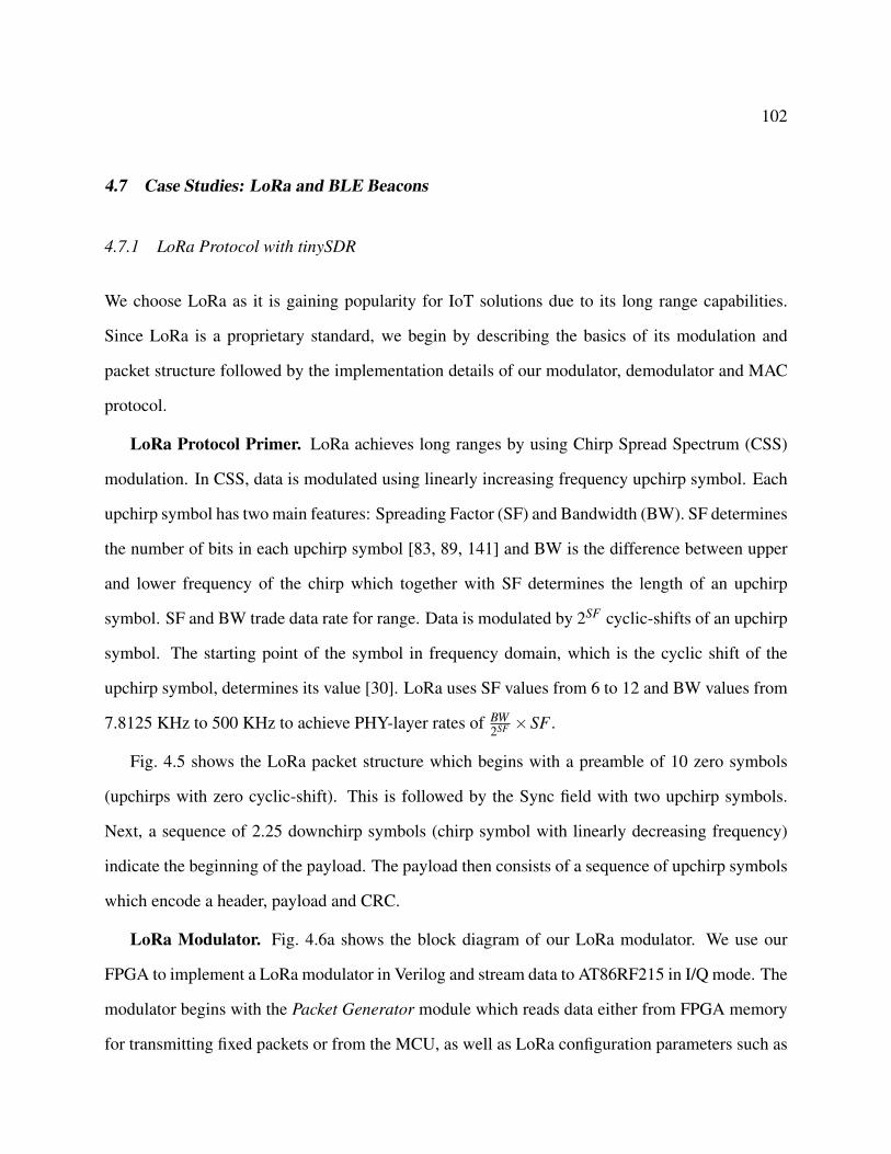
102
4.7 Case Studies: LoRa and BLE Beacons
4.7.1 LoRa Protocol with tinySDR
We choose LoRa as it is gaining popularity for IoT solutions due to its long range capabilities.
Since LoRa is a proprietary standard, we begin by describing the basics of its modulation and
packet structure followed by the implementation details of our modulator, demodulator and MAC
protocol.
LoRa Protocol Primer. LoRa achieves long ranges by using Chirp Spread Spectrum (CSS)
modulation. In CSS, data is modulated using linearly increasing frequency upchirp symbol. Each
upchirp symbol has two main features: Spreading Factor (SF) and Bandwidth (BW). SF determines
the number of bits in each upchirp symbol [83, 89, 141] and BW is the difference between upper
and lower frequency of the chirp which together with SF determines the length of an upchirp
symbol. SF and BW trade data rate for range. Data is modulated by 2SF cyclic-shifts of an upchirp
symbol. The starting point of the symbol in frequency domain, which is the cyclic shift of the
upchirp symbol, determines its value [30]. LoRa uses SF values from 6 to 12 and BW values from
7.8125 KHz to 500 KHz to achieve PHY-layer rates of BW2SF ×SF .
Fig. 4.5 shows the LoRa packet structure which begins with a preamble of 10 zero symbols
(upchirps with zero cyclic-shift). This is followed by the Sync field with two upchirp symbols.
Next, a sequence of 2.25 downchirp symbols (chirp symbol with linearly decreasing frequency)
indicate the beginning of the payload. The payload then consists of a sequence of upchirp symbols
which encode a header, payload and CRC.
LoRa Modulator. Fig. 4.6a shows the block diagram of our LoRa modulator. We use our
FPGA to implement a LoRa modulator in Verilog and stream data to AT86RF215 in I/Q mode. The
modulator begins with the Packet Generator module which reads data either from FPGA memory
for transmitting fixed packets or from the MCU, as well as LoRa configuration parameters such as
103
SF, coding and BW. This module determines each symbol value and its corresponding cyclic-shift.
Next, the Packet Generator sends these parameters along with the symbol values to the Chirp
Generator module, which generates the I/Q samples of each chirp symbol in the packet using a
squared phase accumulator and two lookup tables for sine and cosine function [141]. We then feed
these I/Q samples into an I/Q Serializer to stream them over the LVDS interface to the I/Q radio.
We generate the 64 MHz transmission clock using internal PLL of the FPGA.
LoRa Demodulator. Fig. 4.6b shows the block diagram of our LoRa demodulator. It begins
by reading data from the I/Q radio into the I/Q Deserializer module on the FPGA which converts
the serial I/Q stream to parallel I/Q for further signal processing. Next, we run the data through a
14 tap FIR low-pass filter to suppress high frequency noise and interference. We store the filtered
samples in a buffer implemented using the FPGA’s memory blocks. To decode the data, we use
the Chirp Generator module from the LoRa Modulator described above to generate a baseline
upchirp/downchirp symbol, and then we multiply that with the received chirp symbol using our
Complex Multiplier unit. The output of the multiplication then goes to an FFT block implemented
using a standard IP core from Lattice. Finally the Symbol Detector scans the output of the FFT for
peaks and records the frequency of the peak to determine the symbol value. To detect the chirp type
(upchirp/downchirp), we multiply each chirp symbol with both an upchirp and downchirp and then
compare the amplitudes of their FFT peaks. The higher peak in the FFT shows higher correlation
which indicates the chirp type.
LoRa MAC Layer. To demonstrate that our LoRa implementation on tinySDR is compatible
with existing LoRa networks such as the LoRa Alliance’s [50] The Things Network (TTN) [65], we
adopt their LoRa MAC design from TTN’s Arduino libraries [66] and implement it on tinySDR’s
MCU. TTN uses two methods for device association; Over-the-air activation (OTAA) and acti-
vation by personalization (ABP). In OTAA, each node performs a join-procedure during which
a dynamic device address is assigned to a node. However, in ABP we can hard-code the device
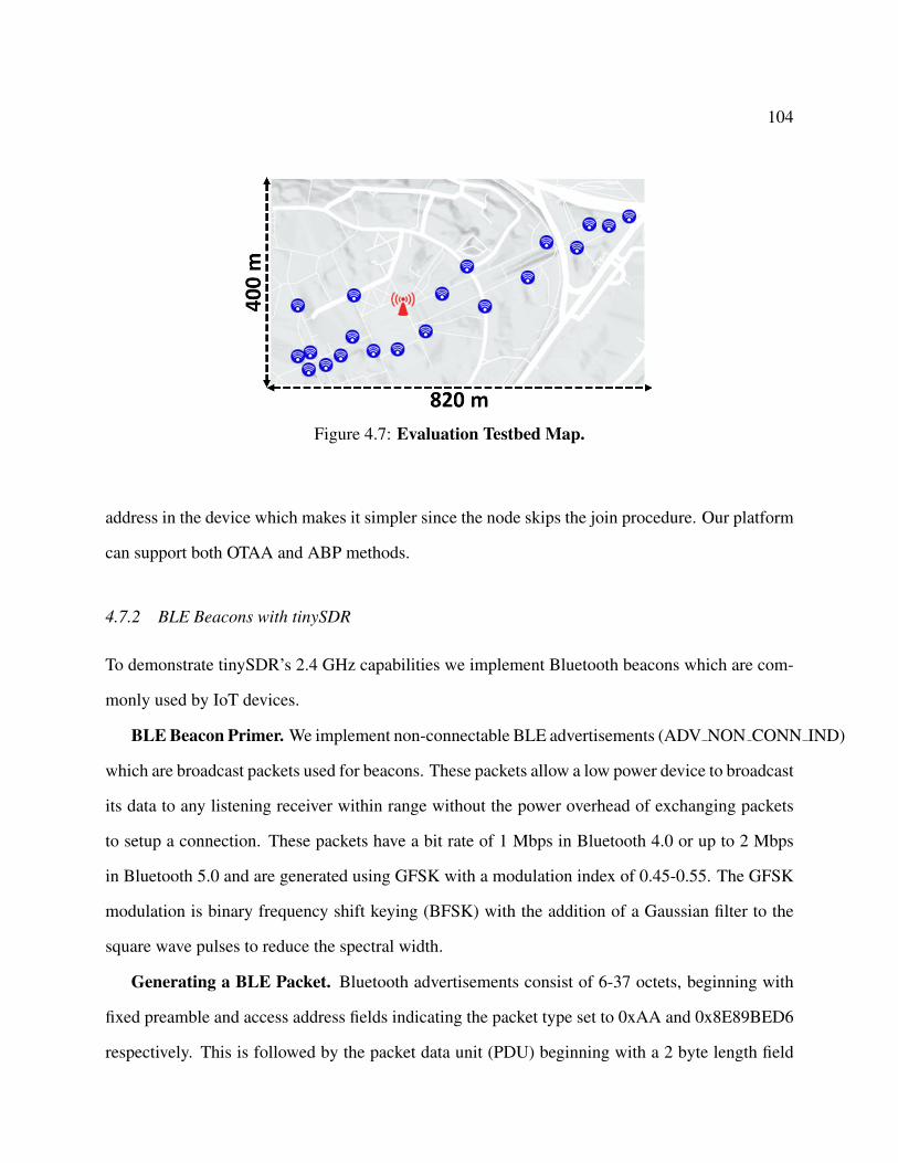
104
Figure 4.7: Evaluation Testbed Map.
address in the device which makes it simpler since the node skips the join procedure. Our platform
can support both OTAA and ABP methods.
4.7.2 BLE Beacons with tinySDR
To demonstrate tinySDR’s 2.4 GHz capabilities we implement Bluetooth beacons which are com-
monly used by IoT devices.
BLE Beacon Primer. We implement non-connectable BLE advertisements (ADV NON CONN IND)
which are broadcast packets used for beacons. These packets allow a low power device to broadcast
its data to any listening receiver within range without the power overhead of exchanging packets
to setup a connection. These packets have a bit rate of 1 Mbps in Bluetooth 4.0 or up to 2 Mbps
in Bluetooth 5.0 and are generated using GFSK with a modulation index of 0.45-0.55. The GFSK
modulation is binary frequency shift keying (BFSK) with the addition of a Gaussian filter to the
square wave pulses to reduce the spectral width.
Generating a BLE Packet. Bluetooth advertisements consist of 6-37 octets, beginning with
fixed preamble and access address fields indicating the packet type set to 0xAA and 0x8E89BED6
respectively. This is followed by the packet data unit (PDU) beginning with a 2 byte length field
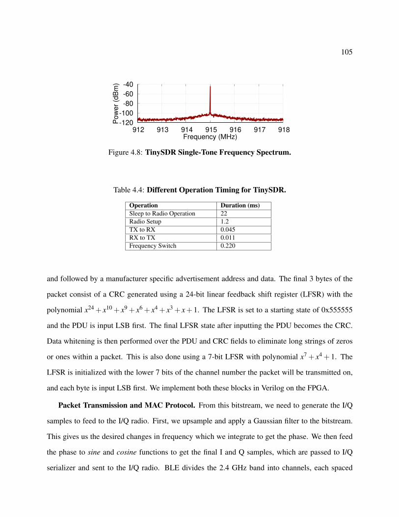
105
-120
-100
-80
-60
-40
912 913 914 915 916 917 918
Po
we
r (d
Bm
)
Frequency (MHz)
Figure 4.8: TinySDR Single-Tone Frequency Spectrum.
Table 4.4: Different Operation Timing for TinySDR.
Operation Duration (ms)Sleep to Radio Operation 22Radio Setup 1.2TX to RX 0.045RX to TX 0.011Frequency Switch 0.220
and followed by a manufacturer specific advertisement address and data. The final 3 bytes of the
packet consist of a CRC generated using a 24-bit linear feedback shift register (LFSR) with the
polynomial x24 + x10 + x9 + x6 + x4 + x3 + x+ 1. The LFSR is set to a starting state of 0x555555
and the PDU is input LSB first. The final LFSR state after inputting the PDU becomes the CRC.
Data whitening is then performed over the PDU and CRC fields to eliminate long strings of zeros
or ones within a packet. This is also done using a 7-bit LFSR with polynomial x7 + x4 + 1. The
LFSR is initialized with the lower 7 bits of the channel number the packet will be transmitted on,
and each byte is input LSB first. We implement both these blocks in Verilog on the FPGA.
Packet Transmission and MAC Protocol. From this bitstream, we need to generate the I/Q
samples to feed to the I/Q radio. First, we upsample and apply a Gaussian filter to the bitstream.
This gives us the desired changes in frequency which we integrate to get the phase. We then feed
the phase to sine and cosine functions to get the final I and Q samples, which are passed to I/Q
serializer and sent to the I/Q radio. BLE divides the 2.4 GHz band into channels, each spaced
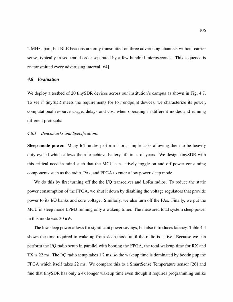
106
2 MHz apart, but BLE beacons are only transmitted on three advertising channels without carrier
sense, typically in sequential order separated by a few hundred microseconds. This sequence is
re-transmitted every advertising interval [64].
4.8 Evaluation
We deploy a testbed of 20 tinySDR devices across our institution’s campus as shown in Fig. 4.7.
To see if tinySDR meets the requirements for IoT endpoint devices, we characterize its power,
computational resource usage, delays and cost when operating in different modes and running
different protocols.
4.8.1 Benchmarks and Specifications
Sleep mode power. Many IoT nodes perform short, simple tasks allowing them to be heavily
duty cycled which allows them to achieve battery lifetimes of years. We design tinySDR with
this critical need in mind such that the MCU can actively toggle on and off power consuming
components such as the radio, PAs, and FPGA to enter a low power sleep mode.
We do this by first turning off the the I/Q transceiver and LoRa radios. To reduce the static
power consumption of the FPGA, we shut it down by disabling the voltage regulators that provide
power to its I/O banks and core voltage. Similarly, we also turn off the PAs. Finally, we put the
MCU in sleep mode LPM3 running only a wakeup timer. The measured total system sleep power
in this mode was 30 uW.
The low sleep power allows for significant power savings, but also introduces latency. Table 4.4
shows the time required to wake up from sleep mode until the radio is active. Because we can
perform the I/Q radio setup in parallel with booting the FPGA, the total wakeup time for RX and
TX is 22 ms. The I/Q radio setup takes 1.2 ms, so the wakeup time is dominated by booting up the
FPGA which itself takes 22 ms. We compare this to a SmartSense Temperature sensor [26] and
find that tinySDR has only a 4x longer wakeup time even though it requires programming unlike
107
230
240
250
260
270
280
290
-14 -12 -10 -8 -6 -4 -2 0 2 4 6 8 10 12 14
Pow
er
Consum
ption (
mW
)
Radio Output Power (dBm)
tinySDR 900 MHztinySDR 2.4 GHz
Figure 4.9: Single-Tone Transmitter Power Consumption. We show the total power consump-tion of tinySDR including I/Q radio, FPGA, MCU and regulators at different transmitter outputpower. This is 15-16 times lower power consumption than the USRP E310 embedded SDR.
commercial products that use a custom single protocol radio. Additionally many IoT devices
operate at low duty cycles waiting in sleep mode for seconds or more making tinySDR’s wakeup
latency insignificant.
Switching delays. We also measure the switching delays for different operations on the I/Q
radio as this is an important parameter for meeting MAC and protocol timing requirements. Ta-
ble 4.4 shows that it takes 45 µs and 11 µs to switch from TX to RX mode and RX to TX mode
respectively. As we see later, this is sufficient to meet the timing requirements of IoT packet
ACKs and MAC protocols. Further, the delay for switching between different frequencies is only
220 us. To measure this number, we switch between 2.402 GHz, 2.426 GHz and 2.480 GHz. This
switching delay is again sufficient to meet the requirements of frequency hopping during Bluetooth
advertising.
Transmitter performance. First, we implement a single-tone modulator on the FPGA that
generates the appropriate I/Q samples and streams them over LVDS to the radio. We connect the
output to an MDO4104b-6 [22] spectrum analyzer and observe a single tone, shown in Fig. 4.8,
with no unexpected harmonics introduced by the modulator.
Next we measure the end-to-end DC power consumption of our system including the I/Q radio,
FPGA, MCU and regulators to see how it scales with RF output power. We vary our radio output
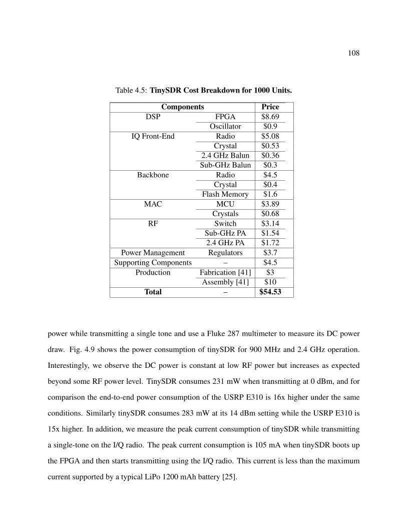
108
Table 4.5: TinySDR Cost Breakdown for 1000 Units.
Components PriceDSP FPGA $8.69
Oscillator $0.9IQ Front-End Radio $5.08
Crystal $0.532.4 GHz Balun $0.36Sub-GHz Balun $0.3
Backbone Radio $4.5Crystal $0.4
Flash Memory $1.6MAC MCU $3.89
Crystals $0.68RF Switch $3.14
Sub-GHz PA $1.542.4 GHz PA $1.72
Power Management Regulators $3.7Supporting Components – $4.5
Production Fabrication [41] $3Assembly [41] $10
Total – $54.53
power while transmitting a single tone and use a Fluke 287 multimeter to measure its DC power
draw. Fig. 4.9 shows the power consumption of tinySDR for 900 MHz and 2.4 GHz operation.
Interestingly, we observe the DC power is constant at low RF power but increases as expected
beyond some RF power level. TinySDR consumes 231 mW when transmitting at 0 dBm, and for
comparison the end-to-end power consumption of the USRP E310 is 16x higher under the same
conditions. Similarly tinySDR consumes 283 mW at its 14 dBm setting while the USRP E310 is
15x higher. In addition, we measure the peak current consumption of tinySDR while transmitting
a single-tone on the I/Q radio. The peak current consumption is 105 mA when tinySDR boots up
the FPGA and then starts transmitting using the I/Q radio. This current is less than the maximum
current supported by a typical LiPo 1200 mAh battery [25].
109
Cost. We also analyze the cost which is an important practical consideration for real world
deployment at scale. Table 4.5 shows a detailed breakdown of cost including each component as
well as PCB fabrication and assembly based on quotes for 1000 units [41], where the overall cost
is around $55 each.
4.8.2 Evaluating the Case Studies
LoRa using tinySDR. We evaluate various different components of tinySDR using LoRa as a case
study.
LoRa modulator. To evaluate this, we use our LoRa modulator to generate packets with three
byte payloads using a spreading factor of SF = 8 and bandwidths of 250 kHz and 125 kHz
which we transmit at -13 dBm. We receive the output of tinySDR on a Semtech SX1276 LoRa
transceiver [62] which we use to measure the packet error rate (PER) versus RSSI and plot the
results in Fig. 4.10. We compare our LoRa modulator to transmissions from an SX1276 LoRa
transceiver. The plots show that we can achieve a comparable sensitivity of -126 dBm which is
the LoRa sensitivity for SF = 8 and BW = 125kHz configuration. This is true for both configura-
tions, which shows that our low-power SDR can meet the sensitivity requirement of LPWAN IoT
protocols.
LoRa demodulator. Next we evaluate our LoRa demodulator on tinySDR. To test this, we
use transmissions from a Semtech SX1276 LoRa transceiver and use tinySDR to receive these
transmissions. The LoRa transceiver transmits packets with two configurations using a spreading
factor of 8 and bandwidths of 250 kHz and 125 kHz. We record the received RF signals in the
FPGA memory and run them through our demodulator to compute a chirp symbol error rate. Note
that the Semtech LoRa transceiver does not give access to its symbol error rate, but since we have
access to I/Q samples, we can compute it on our platform. We plot the results in Fig. 4.11 as a
function of the LoRa RSSI values. Our LoRa demodulator can demodulate chirp symbols down

110
0 20 40 60 80
100
-135 -130 -125 -120 -115 -110 -105 -100 -95
PE
R (
%)
RSSI (dBm)
TinySDR: SF8, BW250kHzTinySDR: SF8, BW125kHzSX1276: SF8, BW250kHzSX1276: SF8, BW125kHz
Figure 4.10: LoRa Modulator Evaluation. We evaluate our LoRa modulator in comparison withSemtech LoRa chip.
0 20 40 60 80
100
-140 -135 -130 -125 -120 -115 -110 -105 -100
Ch
irp
Sym
bo
lE
rro
r R
ate
(%)
RSSI (dBm)
SF8, BW250kHzSF8, BW125kHz
SF8, BW250k SensitivitySF8, BW125k Sensitivity
Figure 4.11: LoRa Demodulator Evaluation. We evaluate our LoRa demodulator by demodulat-ing chirp symbols at different RSSI.
to -126 dBm which is LoRa protocol sensitivity at SF = 8 and BW = 125kHz. Both the LoRa
modulator and demodulator run in real-time.
Resource allocation. Next, we evaluate the resource utilization of our LoRa PHY implemen-
tation on the FPGA. Table 4.6 shows the size for implementing the modulator and demodulator
on our FPGA using different SFs. Our LoRa modulator supports all LoRa configurations with
different SF with no additional cost. However, in the LoRa demodulator, we need FFT blocks with
different sizes to support different SF configurations. This table shows that our FPGA has suffi-
cient resources to support multiple configurations of LoRa and still leave space for other custom
operations.
LoRa MAC. We implement the LoRa MAC based on TTN’s Arduino libraries [66]. TTN pro-
tocol together with control for the I/Q radio, backbone radio, FPGA, PMU and decompression
algorithm for OTA take only 18% of MCU resources. Also, as shown in Table 4.4, our timings are
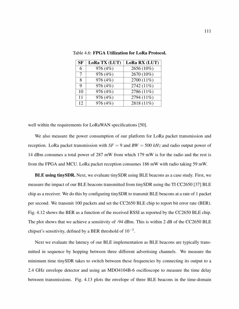
111
Table 4.6: FPGA Utilization for LoRa Protocol.
SF LoRa TX (LUT) LoRa RX (LUT)6 976 (4%) 2656 (10%)7 976 (4%) 2670 (10%)8 976 (4%) 2700 (11%)9 976 (4%) 2742 (11%)10 976 (4%) 2786 (11%)11 976 (4%) 2794 (11%)12 976 (4%) 2818 (11%)
well within the requirements for LoRaWAN specifications [50].
We also measure the power consumption of our platform for LoRa packet transmission and
reception. LoRa packet transmission with SF = 9 and BW = 500 kHz and radio output power of
14 dBm consumes a total power of 287 mW from which 179 mW is for the radio and the rest is
from the FPGA and MCU. LoRa packet reception consumes 186 mW with radio taking 59 mW.
BLE using tinySDR. Next, we evaluate tinySDR using BLE beacons as a case study. First, we
measure the impact of our BLE beacons transmitted from tinySDR using the TI CC2650 [37] BLE
chip as a receiver. We do this by configuring tinySDR to transmit BLE beacons at a rate of 1 packet
per second. We transmit 100 packets and set the CC2650 BLE chip to report bit error rate (BER).
Fig. 4.12 shows the BER as a function of the received RSSI as reported by the CC2650 BLE chip.
The plot shows that we achieve a sensitivity of -94 dBm. This is within 2 dB of the CC2650 BLE
chipset’s sensitivity, defined by a BER threshold of 10−3.
Next we evaluate the latency of our BLE implementation as BLE beacons are typically trans-
mitted in sequence by hopping between three different advertising channels. We measure the
minimum time tinySDR takes to switch between these frequencies by connecting its output to a
2.4 GHz envelope detector and using an MDO4104B-6 oscilloscope to measure the time delay
between transmissions. Fig. 4.13 plots the envelope of three BLE beacons in the time-domain

112
transmitted on the different advertising channels and shows that our system can transmit packets
with as little as 220 us delay between beacons. The corresponding result when a iPhone 8 transmits
beacons is 350 us. Finally, generating BLE beacons requires only 3% of the FPGA resources on
the tinySDR and it could run for over 2 years on a 1000 mAh battery when transmitting once per
second.
4.8.3 Over-the-Air Programming
An effective OTA programming system should both minimize use of system resources such as
power as well as network downtime. Considering the time to reprogram the FPGA and microcon-
troller from flash is fixed, the downtime for programming a node depends on the amount of data
sent and the throughput which varies with SNR.
Raw programming files for our FPGA are 579 kB, however we compress our data using
miniLZO. While the exact compression ratio depends on FPGA utilization, our LoRa program
compresses to 99 kB and BLE to 40 kB. Our microcontroller programs for both LoRa and BLE
are approximately 78 kB and are both compressed to 24 kB. When dividing the files into packets,
we would ideally minimize the preamble length and maximize packet length to reduce overhead,
however long packets with short preambles lead to higher PER. We choose a preamble of 8 chirps
and packets of 60 B which we find balances the trade-off of protocol overhead versus range in our
experiments.
To see the impact on a real deployment, we evaluate the time required to program tinySDR
nodes in our 20 device testbed shown in Fig. 4.7. We set up a LoRa transceiver configured with
SF = 8, BW = 500 kHz and CodingRate = 6 connected to a patch antenna transmitting at 14 dBm
as an AP and measure the time it takes to program the tinySDR devices at each location, according
to our protocol. We transmit the compressed FPGA and MCU programming data for LoRa and
BLE and plot the results as a CDF in Fig. 4.14. The plots show that the LoRa FPGA requires an
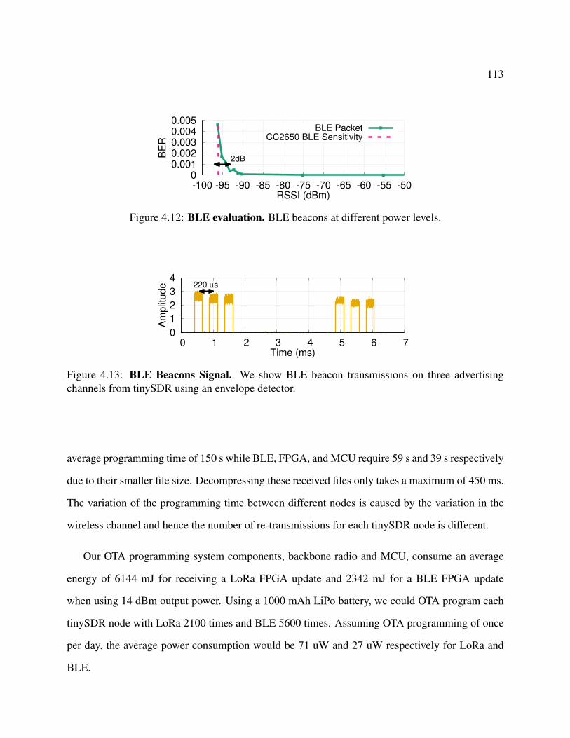
113
0 0.001 0.002 0.003 0.004 0.005
-100 -95 -90 -85 -80 -75 -70 -65 -60 -55 -50
BE
R
RSSI (dBm)
BLE PacketCC2650 BLE Sensitivity
2dB
Figure 4.12: BLE evaluation. BLE beacons at different power levels.
0
1
2
3
4
0 1 2 3 4 5 6 7
Am
plit
ud
e
Time (ms)
220 µs
Figure 4.13: BLE Beacons Signal. We show BLE beacon transmissions on three advertisingchannels from tinySDR using an envelope detector.
average programming time of 150 s while BLE, FPGA, and MCU require 59 s and 39 s respectively
due to their smaller file size. Decompressing these received files only takes a maximum of 450 ms.
The variation of the programming time between different nodes is caused by the variation in the
wireless channel and hence the number of re-transmissions for each tinySDR node is different.
Our OTA programming system components, backbone radio and MCU, consume an average
energy of 6144 mJ for receiving a LoRa FPGA update and 2342 mJ for a BLE FPGA update
when using 14 dBm output power. Using a 1000 mAh LiPo battery, we could OTA program each
tinySDR node with LoRa 2100 times and BLE 5600 times. Assuming OTA programming of once
per day, the average power consumption would be 71 uW and 27 uW respectively for LoRa and
BLE.
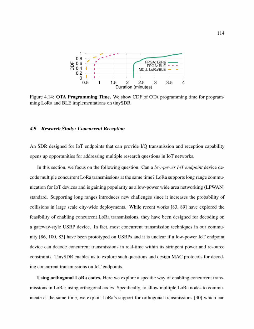
114
0 0.2 0.4 0.6 0.8
1
0.5 1 1.5 2 2.5 3 3.5 4
CD
F
Duration (minutes)
FPGA: LoRaFPGA: BLE
MCU: LoRa/BLE
Figure 4.14: OTA Programming Time. We show CDF of OTA programming time for program-ming LoRa and BLE implementations on tinySDR.
4.9 Research Study: Concurrent Reception
An SDR designed for IoT endpoints that can provide I/Q transmission and reception capability
opens up opportunities for addressing multiple research questions in IoT networks.
In this section, we focus on the following question: Can a low-power IoT endpoint device de-
code multiple concurrent LoRa transmissions at the same time? LoRa supports long range commu-
nication for IoT devices and is gaining popularity as a low-power wide area networking (LPWAN)
standard. Supporting long ranges introduces new challenges since it increases the probability of
collisions in large scale city-wide deployments. While recent works [83, 89] have explored the
feasibility of enabling concurrent LoRa transmissions, they have been designed for decoding on
a gateway-style USRP device. In fact, most concurrent transmission techniques in our commu-
nity [86, 100, 83] have been prototyped on USRPs and it is unclear if a low-power IoT endpoint
device can decode concurrent transmissions in real-time within its stringent power and resource
constraints. TinySDR enables us to explore such questions and design MAC protocols for decod-
ing concurrent transmissions on IoT endpoints.
Using orthogonal LoRa codes. Here we explore a specific way of enabling concurrent trans-
missions in LoRa: using orthogonal codes. Specifically, to allow multiple LoRa nodes to commu-
nicate at the same time, we exploit LoRa’s support for orthogonal transmissions [30] which can
115
occupy the same frequency channel without interfering with each other. Two chirp symbols are
orthogonal when they have a different chirp slope. For a chirp with a spreading factor of SF and
bandwidth of BW , the chirp slope is given by: BW 2
2SF [89].
Decoding concurrent transmissions on tinySDR. In order to receive concurrent LoRa trans-
missions, tinySDR must be able to demodulate LoRa upchirp symbols with different slopes. Sup-
pose we have two LoRa transmissions that use different spreading factor and bandwidth configu-
rations: SF1,BW1 and SF2,BW2. To decode them concurrently, we implement decoders similar to
Fig. 4.6b for each chirp configuration in parallel on our FPGA. Specifically, we first generate a cor-
responding downchirp symbol for each configuration in real-time using our chirp generator. Note
that we generate each chirp with its corresponding configuration on the FPGA and we do not use
pre-generated chirps on the FPGA. We then correlate the received signals with their corresponding
downchirp symbols using time domain multiplication. After correlation, we take the appropriate
length FFT of the result.
Evaluation. We evaluate three key aspects of our design: 1) the platform’s effectiveness in
decoding concurrent transmissions across a range of RSSI values, 2) the power consumption at
the endpoint device while decoding concurrent transmissions and 3) the computational resources
required.
We use two SX1276 LoRa transceivers as our transmitters and set them to transmit continu-
ously at two different settings: they both use a spreading factor of SF = 8 but have two different
bandwidth setups, BW1 = 125kHz and BW2 = 250kHz. We set the two to send random chirp sym-
bols. The tinySDR platform decodes these two concurrent transmissions and computes the chirp
symbol error rate for each transmission. We evaluate two scenarios: 1) when the two transmitters
have a similar power level at the receiver, 2) fix the power of one of the transmitters and increase
the power of the other one.
Fig. 4.15a shows the results when the two transmissions have similar power at the receiver. We

116
lose around 2 dB and 0.5 dB sensitivity for concurrent demodulation of LoRa configurations with
BW1 = 125kHz and BW2 = 250kHz. This is because while in theory the two chirps are orthogo-
nal, in practice, the chirps are created in the digital domain with discrete frequency steps which
introduces some non-orthogonality.
Fig. 4.15b shows the results when the first LoRa transmitter BW1 = 125kHz is received near its
sensitivity of -123 dBm and and the second LoRa transmitter changes its power. Here, the chirp
symbol error rate is affected when the other transmission’s power is higher than -116 dBm. When
two concurrent transmissions are present, one acts as an interferer when decoding the other. The
combined power of noise and the interferer, PI,N , determines the error rate. When sweeping the
power of interferer, at first the PI,N is dominated by noise and we should not see much effect on
error rate. Then at some point their power would be equal which results in a 3 dB increase of PI,N
and hence 3 dB sensitivity loss after which the error rate is determined by the interferer power.
This demonstrates the need for power control for concurrent transmissions to be received on IoT
endpoints.
Our parallel demodulation implementation, uses only 17% of the FPGA resources. This con-
current demodulation implementation consumes 207 mW. Note that Semtech gateway solutions
such as the SX1308 [55] can receive multiple transmissions. But, to the best of our knowledge we
are the first to show that concurrent LoRa transmissions can be decoded on an IoT endpoint while
meeting its power and computational requirements. This would have been difficult to do without
tinySDR.
4.10 Conclusion and Research Opportunities
This chapter presents the first SDR platform specifically tailored to the needs of IoT endpoints that
can be used for large scale IoT network deployments. The goal of LoRa backscatteris to provide a
platform that can catalyze research in IoT networks.

117
0 20 40 60 80
100
-130 -125 -120 -115 -110 -105 -100
Ch
irp
Sym
bo
lE
rro
r R
ate
(%)
RSSI (dBm)
SF8, BW250kHzSF8, BW125kHz
SF8, BW250k SensitivitySF8, BW125k Sensitivity
(a) Orthogonal Transmissions with Same Received Signal Power.
0 20 40 60 80
100
-130 -125 -120 -115 -110 -105
Ch
irp
Sym
bo
lE
rro
r R
ate
(%)
Interference Signal Power (dBm)
SF8, BW125kHz
NoiseDominant
InterferenceDominant
(b) Orthogonal Transmissions with Different Received Signal Power. We set the power of LoRa transmission with BW1 = 125kHz to -123 dBmand increase the power of the other one.
Figure 4.15: Orthogonal LoRa Demodulation Evaluation
Research on PHY/MAC protocols. LoRa backscatterpresents an opportunity for researchers
to avoid the time consuming endeavor of building their own custom hardware and instead focus on
PHY/MAC protocol innovations across the stack: What is the trade-off between packet length and
overall throughput? Are there benefits of rate adaptation? What about concurrent transmissions
from IoT devices? One could also create multi-hop IoT PHY/MAC innovations, which have not
been explored well given the lack of a flexible platform.
Research on IoT localization. LoRa backscattercould also be used to build localization sys-
tems as it gives access to I/Q signals and therefore phase across the 2.4 GHz and 900 MHz bands,
which forms the basis for many localization algorithms[118]. One could also explore distributed
localization solutions that combine the phase information across a distributed set of sensors to
create a large MIMO sensing system.
118
Machine learning on IoT devices. The FPGA on LoRa backscatteropens up exciting oppor-
tunities [74] for exploring machine learning algorithms on-board. This would allow researchers
to explore trade-offs between the power overhead of running an on-board classifier versus send-
ing data to the cloud. This could also enable use of high bandwidth sensors such as cameras and
microphones where the power bottleneck may be communication rather than sensing.
Low power backscatter readers. Recent work on ambient backscatter [111, 101, 102, 96, 149]
aims to achieve ultra-low power communication for IoT devices. Many of these proposals re-
quire either a single-tone generator [102] or a custom receiver to decode the backscatter transmis-
sions [131, 95, 94, 116]. TinySDR can be used as a building block to achieve a battery-operated
backscatter signal generation and receiver.
Better programming interface and protocols. In addition to IoT research opportunities, we
can also improve our platform in multiple ways. TinySDR currently requires users to write Verilog
or VHDL to program the FPGA and C code for programming the microcontroller. Future versions
can incorporate a pipeline to use high level synthesis tools or integrate with GNUradio for easy
prototyping. Further, LoRa backscatteruses a simple MAC protocol for programming with a focus
on using minimal system resources to allow for other custom software; however we could explore
modified MAC protocols that simultaneously broadcast the updates across the network to reduce
programming time.
119
Chapter 5
CONCLUSION
In conclusion, this dissertation presents wireless protocols that are well-suited for ultra low-
power IoT applications and a platform which paves the way for the research community to develop
and innovate on IoT protocols. Specifically, we designed wireless protocols and coding schemes
to extend the range of backscatter communication systems and enable concurrent transmissions.
Furthermore, we showed a flexible wireless platform that can emulate an actual IoT endpoint. We
evaluated these systems and deployed them in various practical scenarios.
• LoRa Backscatter: Enabling The Vision of Ubiquitous Connectivity. We overturned the
conventional wisdom about the backscatter technologies and presented the first wide-area
backscatter system. We enabled this by using CSS coding and showed that we can achieve
several hundreds of meter range using this technology.
• NetScatter: Enabling Large-Scale Backscatter Networks. We presented the first wireless
protocol that scales to hundreds of concurrent transmissions from backscatter devices while
being low power and long-range. We developed a distributed coding mechanism that works
below the noise floor, operates on backscatter devices and can decode all the concurrent
transmissions at the receiver using a single FFT operation.
• TinySDR: Low-Power SDR Platform for Over-the-Air Programmable IoT Testbeds. We built
the first SDR platform tailored to the needs of power-constrained IoT endpoints. TinySDR
provides a standalone, fully programmable low power software-defined radio solution that
120
can be duty cycled for battery operation like a real IoT endpoint, and more importantly, can
be programmed over the air to allow for large scale deployment.
5.1 Looking Forward
Over the past few years, IoT devices have seen a rapid proliferation. Tradeoffs exist between com-
puting and communication across battery-powered, battery-free and other resource-constrained IoT
devices. These devices span HD cameras located at long-ranges within a city, humidity sensors de-
ployed at farms, implanted and wearable sensors with unfavorable wireless channel conditions and
AR/VR devices. The focus of this dissertation was on the power and wireless communication as-
pect of these systems. However, to build an end to end IoT solutions, we need to understand and
address the latency requirements, battery and size constraints, available compute resources on the
edge and wireless communication channel to the cloud while considering power, range and privacy
concerns. For example, in smart homes and smart cities, what kind wireless communication we
need to enable a low power city scale network? How should we divide computing tasks between
the sensor node and the cloud? Can we make these sensor nodes cooperate to share computing
resources? How can we resolve privacy concerns? How can we address latency constraints? For
example, a city scale video analytics system designed to help autonomous vehicles’ applications
has very different latency requirements compared to a pollution sensor node deployed in a city.
Answering these questions to develop an end to end IoT solutions is the subject of the future
work.
121
BIBLIOGRAPHY
[1] 915mhz whip, straight rf antenna by nearson. ftp://ftp2.nearson.com/Drawings/
Antenna/S463XX-915.pdf.
[2] Alien swiggle rfid tag. http://www.rfidtags.com/squiggle-h3-rfid-tag.
[3] Altera’s cyclone v fpgas. https://www.altera.com/products/fpga/
cyclone-series/cyclone-v/overview.html.
[4] bladerf 2.0 micro. https://www.nuand.com/bladeRF_2_micro-brief.pdf.
[5] Brightvolt product matrix. http://www.brightvolt.com/products/
product-matrix-2/.
[6] Cadence rfspectre. http://www.cadence.com/products/rf/spectre_rf_
simulation/pages/default.aspx.
[7] De0-cv development kit. http://www.terasic.com.tw/cgi-bin/page/archive.pl?
Language=English&CategoryNo=163&No=921&PartNo=2.
[8] EFL700A39- rechargable thin film batteries by stmicroelectronics. http:
//www.st.com/content/ccc/resource/technical/document/datasheet/
cd/ac/89/0b/b4/8e/43/0b/CD00270103.pdf/files/CD00270103.pdf/jcr:
content/translations/en.CD00270103.pdf.
[9] Flexible, printed and thin film batteries 2016-2026: Technologies, mar-kets, players. http://www.idtechex.com/en/research-report/
flexible-printed-and-thin-film-batteries-2019-2029/634.
[10] Limesdr. https://myriadrf.org/projects/limesdr/.
[11] Limesdr-mini. https://wiki.myriadrf.org/LimeSDR-Mini.
[12] Lte for iot. http://resources.alcatel-lucent.com/asset/200178.
[13] An overview of lvds technology. http://www.ti.com/lit/an/snla165/snla165.pdf.

122
[14] Rtlsdr rtl2832u dvb-t tuner dongles. https://www.rtl-sdr.com/
buy-rtl-sdr-dvb-t-dongles/.
[15] Synopsis design complier. http://www.synopsys.com/Tools/Implementation/
RTLSynthesis/DesignCompiler/Pages/default.aspx.
[16] Ti cc2650. http://www.digikey.com/product-detail/en/CC2650F128RHBR/
CC2650F128RHBR-ND/5189550.
[17] Usrp b200mini. https://www.ettus.com/content/files/USRP_B200mini_Data_
Sheet.pdf.
[18] Usrp e310. https://www.ettus.com/content/files/USRP_E310_Datasheet.pdf.
[19] 2.45 ghz balun, filter combination, 2003. https://www.mouser.com/datasheet/2/611/JTI_Balun-Filter-2450FB15A050_2006-09-242325.pdf.
[20] Max5189 datasheet, 2003. https://datasheets.maximintegrated.com/en/ds/
MAX5186-MAX5189.pdf.
[21] Max2831 datasheet, 2011. https://datasheets.maximintegrated.com/en/ds/
MAX2831-MAX2832.pdf.
[22] Mdo4000b series datasheet, 2013. http://www.testequipmenthq.com/datasheets/
TEKTRONIX-MDO4104B-6-Datasheet.pdf.
[23] Smart cities and the internet of everything: The foundation for delivering next-generation citizen services, 2013. http://www.cisco.com/c/dam/en_us/solutions/
industries/docs/scc/ioe_citizen_svcs_white_paper_idc_2013.pdf.
[24] Ad9364 transceiver datasheet, 2014. https://www.analog.com/media/en/
technical-documentation/data-sheets/AD9364.pdf.
[25] Li-polymer battery technology specification, 2014. https://cdn-shop.adafruit.
com/product-files/258/C101-_Li-Polymer_503562_1200mAh_3.7V_with_PCM_
APPROVED_8.18.pdf.
[26] Smartsense temp/humidity manual, 2014. https://support.smartthings.com/hc/
en-us/articles/203040294-SmartSense-Temperature-Humidity-Sensor.
[27] 3.5mhz, 500ma synchronous step down dc-dc regulator, 2015. https://www.semtech.
com/uploads/documents/sc195.pdf.

123
[28] Igloo nano fpga datasheet by, 2015. https://www.microsemi.com/document-portal/
doc_download/130695-igloo-nano-low-power-flash-fpgas-datasheet.
[29] The internet of things and the future of farming, 2015. http://bits.blogs.nytimes.
com/2015/08/03/the-internet-of-things-and-the-future-of-farming/?_r=0.
[30] Lora modulation basics, 2015. https://www.semtech.com/uploads/documents/
an1200.22.pdf.
[31] Xrcha-f-a series, 2015. https://www.murata.com/~/media/webrenewal/products/
timingdevice/crystalu/flyers/vppt-hcrj078-d.ashx?la=en-us.
[32] 65 nm cmos process by tsmc, 2016. http://www.tsmc.com/english/
dedicatedFoundry/technology/65nm.htm.
[33] Ad9361 transceiver datasheet, 2016. https://www.analog.com/media/en/
technical-documentation/data-sheets/AD9361.pdf.
[34] Ad9363 transceiver datasheet, 2016. https://www.analog.com/media/en/
technical-documentation/data-sheets/AD9363.pdf.
[35] Adg904 datasheet by analog devices, 2016. http://www.analog.com/media/en/
technical-documentation/data-sheets/ADG904.pdf.
[36] At86rf215 datasheet, 2016.
[37] Cc2650 simplelink datasheet by ti, 2016. http://www.ti.com/lit/ds/symlink/
cc2650.pdf.
[38] How much does an RFID tag cost today?, 2016. https://www.rfidjournal.com/faq/
show?85.
[39] Lora alliance, 2016. https://www.lora-alliance.org/.
[40] New part 15 rules by fcc, 2016. https://transition.fcc.gov/oet/ea/
presentations/files/may05/New_Policies_Pt._15_SD.pdf.
[41] Pcbminions inc., 2016. https://pcbminions.com/.
[42] Se2435l power amplifier datasheet, 2016. http://www.skyworksinc.com/uploads/
documents/SE2435L_202412I.pdf.
124
[43] Semtech sx1276 transceiver, 2016. http://www.semtech.com/wireless-rf/
rf-transceivers/sx1276/.
[44] Sx1276 datasheet by semtech, 2016. https://www.semtech.com/uploads/documents/sx1276.pdf.
[45] Sx1276 datasheet by semtech, 2016. https://www.semtech.com/uploads/documents/sx1276.pdf.
[46] CC2630 by TI, 2017. http://www.ti.com/lit/ds/symlink/cc2630.pdf.
[47] CC2640 by TI, 2017. http://www.ti.com/lit/ds/symlink/cc2640.pdf.
[48] CC3200 SimpleLink Wi-Fi and Internet-of-Things Solution, 2017. http://www.ti.com/
product/CC3200/samplebuy.
[49] Lms7002m datasheet, 2017. https://limemicro.com/app/uploads/2017/07/
LMS7002M-Data-Sheet-v3.1r00.pdf.
[50] Lora alliance, 2017. https://lora-alliance.org/sites/default/files/2018-04/
lorawantm_specification_-v1.1.pdf.
[51] Msp430fr5969 datasheet by ti, 2017. http://www.ti.com/lit/ds/symlink/
msp430fr5969.pdf.
[52] Msp432p401r, msp432p401m simplelink mixed-signal microcontrollers datasheet, 2017.http://www.ti.com/lit/ds/symlink/msp432p401r.pdf.
[53] Sigfox products, 2017.
[54] Sky66112 power amplifier datasheet, 2017. http://www.skyworksinc.com/uploads/
documents/SKY66112_11_203225L.pdf.
[55] Sx1308 datasheet by semtech, 2017. https://www.semtech.com/uploads/documents/sx1308.pdf.
[56] Ad9228 datasheet, 2018. https://www.analog.com/media/en/
technical-documentation/data-sheets/ad9228.pdf.
[57] Adalm-pluto overview, 2018. https://wiki.analog.com/university/tools/pluto.
[58] Atmel at86rf215 868/915/928 mhz impedance matched balun + lpf, 2018. https://www.
mouser.com/datasheet/2/611/0896BM15E0025-1518705.pdf.

125
[59] Lfe5u fpga family datasheet, 2018. http://www.latticesemi.com/view_document?
document_id=50461.
[60] minilzo implementation, 2018. http://www.oberhumer.com/opensource/lzo/
#abstract.
[61] Rf5110 rf power amplifier, 2018. http://www.rfmd.com/store/downloads/dl/file/
id/30508/5110g_product_data_sheet.pdf.
[62] Sx1257 datasheet by semtech, 2018. https://www.semtech.com/uploads/documents/DS_SX1257_V1.2.pdf.
[63] Usrp x-300, 2018. https://www.ettus.com/product/details/X300-KIT.
[64] Bluetooth core specification v5.1, January 2019. https://www.bluetooth.com/
specifications/bluetooth-core-specification.
[65] The things network, 2019. https://www.thethingsnetwork.org/.
[66] The things network arduino library, 2019. https://github.com/TheThingsNetwork/
arduino-device-lib.
[67] Ali Afsahi, Jacob J Rael, Arya Behzad, Hung-Ming Chien, Michael Pan, Stephen Au, Ade-dayo Ojo, C Paul Lee, Seema Butala Anand, Kevin Chien, et al. A low-power single-weight-combiner 802.11 abg soc in 0.13 µm cmos for embedded applications utilizing an area andpower efficient cartesian phase shifter and mixer circuit. IEEE Journal of Solid-State Cir-cuits, 43(5):1101–1118, 2008.
[68] Kiarash Amiri, Yang Sun, Patrick Murphy, Chris Hunter, Joseph R Cavallaro, and AshutoshSabharwal. Warp, a unified wireless network testbed for education and research. In 2007IEEE International Conference on Microelectronic Systems Education (MSE’07), pages 53–54. IEEE, 2007.
[69] Narendra Anand, Ehsan Aryafar, and Edward W Knightly. Warplab: a flexible frameworkfor rapid physical layer design. In Proceedings of the 2010 ACM workshop on Wireless ofthe students, by the students, for the students, pages 53–56. ACM, 2010.
[70] Amay J. Bandodkar and Joseph Wang. Non-invasive wearable electrochemical sensors: areview. Trends in Biotechnology, 32(7):363 – 371, 2014.
[71] A. Berni and W. Gregg. On the utility of chirp modulation for digital signaling. IEEETransactions on Communications, 1973.
126
[72] Katherine Bourzac. Graphene temporary tattoo tracks vital signs. http:
//spectrum.ieee.org/nanoclast/semiconductors/nanotechnology/
graphene-temporary-tattoo.
[73] Ludovic Champion and Nicolas Sornin. Chirp signal processor, 7 2014. European PatentApplication EP2975814A1.
[74] Justin Chan, Anran Wang, Arvind Krishnamurthy, and Shyamnath Gollakota. Deepsense:Enabling carrier sense in low-power wide area networks using deep learning. CoRR,abs/1904.10607, 2019.
[75] Peter KC Chan, Wei Jin, JM Gong, and NS Demokan. Multiplexing of fiber bragg gratingsensors using a fmcw technique. IEEE Photonics Technology Letters, 11(11):1470–1472,1999.
[76] Vipul Chawla and Dong Sam Ha. An overview of passive rfid. IEEE CommunicationsMagazine, 45(9), 2007.
[77] Tzung-Ming Chen, Yung-Ming Chiu, Chun-Cheng Wang, Ka-Un Chan, Ying-Hsi Lin,Ming-Chong Huang, Chao-Hua Lu, Wen-Shan Wang, Che-Sheng Hu, Chao-Cheng Lee,et al. A low-power fullband 802.11 a/b/g wlan transceiver with on-chip pa. IEEE journal ofsolid-state circuits, 42(5):983–991, 2007.
[78] Namjun Cho, Seong-Jun Song, Sunyoung Kim, Shiho Kim, and Hoi-Jun Yoo. A 5.1-/spl µwuhf rfid tag chip integrated with sensors for wireless environmental monitoring. In Solid-State Circuits Conference, 2005. ESSCIRC 2005. Proceedings of the 31st European, pages279–282. IEEE, 2005.
[79] Kun-Da Chu, Mohamad Katanbaf, Chenxin Su, Tong Zhang, and Jacques C Rudell. In-tegrated cmos transceivers design towards flexible full duplex (fd) and frequency divisionduplex (fdd) systems. In 2018 IEEE Custom Integrated Circuits Conference (CICC), pages1–11. IEEE, 2018.
[80] Kun-Da Chu, Mohamad Katanbaf, Tong Zhang, Chenxin Su, and Jacques C Rudell.A broadband and deep-tx self-interference cancellation technique for full-duplex andfrequency-domain-duplex transceiver applications. In 2018 IEEE International Solid-StateCircuits Conference-(ISSCC), pages 170–172. IEEE, 2018.
[81] Daniel MJ Devasirvatham. Time delay spread measurements of wideband radio signalswithin a building. Electronics Letters, 20(23):950–951, 1984.

127
[82] Prabal Dutta, Ye-Sheng Kuo, Akos Ledeczi, Thomas Schmid, and Peter Volgyesi. Puttingthe software radio on a low-calorie diet. In Proceedings of the 9th ACM SIGCOMM Work-shop on Hot Topics in Networks, page 20. ACM, 2010.
[83] Rashad Eletreby, Diana Zhang, Swarun Kumar, and Osman Yagan. Empowering low-powerwide area networks in urban settings. SIGCOMM ’17.
[84] J.F. Ensworth and M.S. Reynolds. Every smart phone is a backscatter reader: Modulatedbackscatter compatibility with bluetooth 4.0 low energy (ble) devices. In RFID, 2015 IEEEInternational Conference on.
[85] Lingzhi Fu, Lirui Liu, Min Li, and Junyu Wang. Collision recovery receiver for epc gen2rfid systems. In Internet of Things (IOT), 2012 3rd International Conference on the, pages114–118, Oct 2012.
[86] Shyamnath Gollakota and Dina Katabi. Zigzag decoding: Combating hidden terminalsin wireless networks. In Proceedings of the ACM SIGCOMM 2008 Conference on DataCommunication, SIGCOMM ’08, 2008.
[87] Yeswanth Guddeti, Raghav Subbaraman, Moein Khazraee, Aaron Schulman, and DineshBharadia. Sweepsense: Sensing 5 ghz in 5 milliseconds with low-cost radios. In 16thUSENIX Symposium on Networked Systems Design and Implementation (NSDI 19),pages 317–330, 2019.
[88] Christian Hambeck, Stefan Mahlknecht, and Thomas Herndl. A 2.4µw wake-up receiverfor wireless sensor nodes with- 71dbm sensitivity. In 2011 IEEE International Symposiumof Circuits and Systems (ISCAS), pages 534–537. IEEE, 2011.
[89] Mehrdad Hessar, Ali Najafi, and Shyamnath Gollakota. Netscatter: Enabling large-scalebackscatter networks. In 16th USENIX Symposium on Networked Systems Design andImplementation (NSDI 19), pages 271–284, 2019.
[90] Ralf Hildebrandt. The pseudo dual-edge d-flip-flop, 2011.
[91] Pan Hu, Pengyu Zhang, and Deepak Ganesan. Laissez-faire: Fully asymmetric backscattercommunication. In Proceedings of the 2015 ACM Conference on Special Interest Group onData Communication, SIGCOMM ’15.
[92] Pan Hu, Pengyu Zhang, and Deepak Ganesan. Leveraging interleaved signal edges forconcurrent backscatter. In hotWireless, 2014.
128
[93] Pan Hu, Pengyu Zhang, and Deepak Ganesan. Laissez-faire: Fully asymmetric backscattercommunication. In Proceedings of the 2015 ACM Conference on Special Interest Group onData Communication, SIGCOMM ’15, pages 255–267, New York, NY, USA, 2015. ACM.
[94] Vikram Iyer, Justin Chan, Ian Culhane, Jennifer Mankoff, and Shyamnath Gollakota. Wire-less analytics for 3d printed objects. In Proceedings of the 31st Annual ACM Symposium onUser Interface Software and Technology, UIST ’18, pages 141–152, New York, NY, USA,2018. ACM.
[95] Vikram Iyer, Justin Chan, and Shyamnath Gollakota. 3d printing wireless connected objects.ACM Trans. Graph., 36(6), November 2017.
[96] Vikram Iyer, Vamsi Talla, Bryce Kellogg, Shyamnath Gollakota, and Joshua Smith. Inter-technology backscatter: Towards internet connectivity for implanted devices. In Proceed-ings of the 2016 ACM SIGCOMM Conference.
[97] Meng Jin, Yuan He, Xin Meng, Yilun Zheng, Dingyi Fang, and Xiaojiang Chen. Fliptracer:Practical parallel decoding for backscatter communication. In Proceedings of the 23rd An-nual International Conference on Mobile Computing and Networking, MobiCom ’17.
[98] Mohamad Katanbaf, Kun-Da Chu, Tong Zhang, Chenxin Su, and Jacques C Rudell. Two-way traffic ahead: Rf\/analog self-interference cancellation techniques and the challengesfor future integrated full-duplex transceivers. IEEE Microwave Magazine, 20(2):22–35,2019.
[99] Mohamad Katanbaf, Vivek Jain, and Joshua R Smith. Relacks: Reliable backscatter commu-nication in indoor environments. Proceedings of the ACM on Interactive, Mobile, Wearableand Ubiquitous Technologies, 4(2):1–24, 2020.
[100] Sachin Katti, Shyamnath Gollakota, and Dina Katabi. Embracing wireless interference:Analog network coding. In ACM SIGCOMM Computer Communication Review, volume 37,pages 397–408. ACM, 2007.
[101] Bryce Kellogg, Aaron Parks, Shyamnath Gollakota, Joshua R. Smith, and David Wetherall.Wi-fi backscatter: Internet connectivity for rf-powered devices. In Proceedings of the 2014ACM Conference on SIGCOMM.
[102] Bryce Kellogg, Vamsi Talla, Shyamnath Gollakota, and Joshua R. Smith. Passive wi-fi:Bringing low power to wi-fi transmissions. In NSDI 16.
[103] Ahmed Khattab, Joseph Camp, Chris Hunter, Patrick Murphy, Ashutosh Sabharwal, and Ed-ward W Knightly. Warp: a flexible platform for clean-slate wireless medium access protocol
129
design. ACM SIGMOBILE Mobile Computing and Communications Review, 12(1):56–58,2008.
[104] Manikanta Kotaru, Pengyu Zhang, and Sachin Katti. Localizing low-power backscatter tagsusing commodity wifi. In CoNext’17.
[105] Ye-Sheng Kuo, Pat Pannuto, Thomas Schmid, and Prabal Dutta. Reconfiguring the softwareradio to improve power, price, and portability. In Proceedings of the 10th ACM Conferenceon Embedded Network Sensor Systems, pages 267–280. ACM, 2012.
[106] Ye-Sheng Kuo, Thomas Schmid, and Prabal Dutta. A compact, inexpensive, and battery-powered software-defined radio platform. In Proceedings of the 11th international confer-ence on Information Processing in Sensor Networks, pages 137–138. ACM, 2012.
[107] Hasnain Lakdawala, Mark Schaecher, Chang-Tsung Fu, Rahul Limaye, Jon Duster, YulinTan, Ajay Balankutty, Erkan Alpman, Chun C Lee, Khoa Minh Nguyen, et al. A 32 nm socwith dual core atom processor and rf wifi transceiver. IEEE Journal of Solid-State Circuits,48(1):91–103, 2013.
[108] Chungyeol Paul Lee, Arya Behzad, Bojko Marholev, Vikram Magoon, Iqbal Bhatti, DandanLi, Subhas Bothra, Ali Afsahi, Dayo Ojo, Rozi Roufoogaran, et al. A multistandard, multi-band soc with integrated bt, fm, wlan radios and integrated power amplifier. In Solid-StateCircuits Conference Digest of Technical Papers (ISSCC), 2010 IEEE International, pages454–455. IEEE, 2010.
[109] Yu-Te Liao, Huanfen Yao, Andrew Lingley, Babak Parviz, and Brian P Otis. A 3-cmosglucose sensor for wireless contact-lens tear glucose monitoring. Solid-State Circuits, IEEEJournal of, 47(1):335–344, 2012.
[110] Yuan Lin, Hyunseok Lee, Mark Woh, Yoav Harel, Scott Mahlke, Trevor Mudge, ChaitaliChakrabarti, and Krisztian Flautner. Soda: A low-power architecture for software radio.ACM SIGARCH Computer Architecture News, 34(2):89–101, 2006.
[111] Vincent Liu, Aaron Parks, Vamsi Talla, Shyamnath Gollakota, David Wetherall, andJoshua R. Smith. Ambient backscatter: Wireless communication out of thin air. SIGCOMM’13.
[112] H. Mahdavifar and A. Vardy. Coding for tag collision recovery. In 2015 IEEE InternationalConference on RFID (RFID), pages 9–16, April 2015.
[113] George Malim. Hot iot is expanding into cosmetics and medical in-dustries. http://www.iotglobalnetwork.com/iotdir/2016/03/22/
how-iot-is-expanding-into-cosmetics-and-medical-industries-1203/.

130
[114] Gary J Minden, Joseph B Evans, Leon Searl, Daniel DePardo, Victor R Petty, Rakesh Ra-jbanshi, T Newman, Qi Chen, F Weidling, J Guffey, et al. Kuar: A flexible software-definedradio development platform. In 2007 2nd IEEE International Symposium on New Frontiersin Dynamic Spectrum Access Networks, pages 428–439. IEEE, 2007.
[115] James Morra. Iot devices and wearables push development ofthin, flexible batteries. http://electronicdesign.com/power/
iot-devices-and-wearables-push-development-thin-flexible-batteries.
[116] Saman Naderiparizi, Mehrdad Hessar, Vamsi Talla, Shyamnath Gollakota, and Joshua RSmith. Towards battery-free hd video streaming. In 15th USENIX Symposium on NetworkedSystems Design and Implementation (NSDI 18), 2018.
[117] Hiroyuki Nakamoto, Daisuke Yamazaki, Takuji Yamamoto, Hajime Kurata, Satoshi Ya-mada, Kenji Mukaida, Tsuzumi Ninomiya, Takashi Ohkawa, Shoichi Masui, and KunihikoGotoh. A passive uhf rf identification cmos tag ic using ferroelectric ram in 0.35 µm tech-nology. IEEE Journal of Solid-State Circuits, 42(1):101–110, 2007.
[118] Rajalakshmi Nandakumar, Vikram Iyer, and Shyamnath Gollakota. 3d localization for sub-centimeter sized devices. In Proceedings of the 16th ACM Conference on Embedded Net-worked Sensor Systems, SenSys ’18, 2018.
[119] Revathy Narayanan and Swarun Kumar. Revisiting software defined radios in the iot era. InProceedings of the 17th ACM Workshop on Hot Topics in Networks. ACM, 2018.
[120] Lalitkumar Nathawad, David Weber, Shahram Abdollahi, Phoebe Chen, Syed Enam, BrianKaczynski, Alireza Kheirkhahi, MeeLan Lee, Sotirios Limotyrakis, Keith Onodera, et al.An ieee 802.11 a/b/g soc for embedded wlan applications. In Solid-State Circuits Confer-ence, 2006. ISSCC 2006. Digest of Technical Papers. IEEE International, pages 1430–1439.IEEE, 2006.
[121] Man Cheuk Ng, Kermin Elliott Fleming, Mythili Vutukuru, Samuel Gross, Hari Balakrish-nan, et al. Airblue: A system for cross-layer wireless protocol development. In Proceedingsof the 6th ACM/IEEE Symposium on Architectures for Networking and CommunicationsSystems, page 4. ACM, 2010.
[122] Jiajue Ou, Mo Li, and Yuanqing Zheng. Come and be served: Parallel decoding for cotsrfid tags. In Proceedings of the 21st Annual International Conference on Mobile Computingand Networking, MobiCom ’15, pages 500–511, New York, NY, USA, 2015. ACM.
[123] J. Pandey, Yu-Te Liao, A. Lingley, R. Mirjalili, B. Parviz, and B. Otis. A fully integratedrf-powered contact lens with a single element display. Biomedical Circuits and Systems,IEEE Transactions on, 2010.
131
[124] Alexandros Pantelopoulos and Nikolaos G Bourbakis. A survey on wearable sensor-basedsystems for health monitoring and prognosis. IEEE Transactions on Systems, Man, andCybernetics, Part C (Applications and Reviews), 40(1):1–12, 2010.
[125] Aaron N. Parks, Angli Liu, Shyamnath Gollakota, and Joshua R. Smith. Turbochargingambient backscatter communication. In Proceedings of the 2014 ACM Conference on SIG-COMM, 2014.
[126] Yao Peng, Longfei Shangguan, Yue Hu, Yujie Qian, Xianshang Lin, Xiaojiang Chen, DingyiFang, and Kyle Jamieson. Plora: a passive long-range data network from ambient loratransmissions. In Proceedings of the 2018 Conference of the ACM Special Interest Groupon Data Communication, SIGCOMM ’18, pages 147–160. ACM, 2018.
[127] Carlos Perez-Penichet, Fredrick Hermans, Ambuj Varshney, and Thiemo Voigt. Augmentingiot networks with backscatter-enabled passive sensor tags. In HotWireless, 2016.
[128] Dinesh Pharadia, Kiran Raj Joshi, Manikanta Kotaru, and Sachin Katti. Backfi: Highthroughput wifi backscatter. In Proceedings of the 2015 ACM Conference on Special In-terest Group on Data Communication, 2015.
[129] Nathan E Roberts and David D Wentzloff. A 98nw wake-up radio for wireless body areanetworks. In 2012 IEEE Radio Frequency Integrated Circuits Symposium, pages 373–376.IEEE, 2012.
[130] Zhiyu Ru, Eric AM Klumperink, and Bram Nauta. A discrete-time mixing receiver archi-tecture with wideband harmonic rejection. In Solid-State Circuits Conference, 2008. ISSCC2008. Digest of Technical Papers. IEEE International, pages 322–616. IEEE, 2008.
[131] Ali Saffari, Mehrdad Hessar, Saman Naderiparizi, and Joshua R Smith. Battery-free wirelessvideo streaming camera system. In 2019 IEEE International Conference on RFID (RFID),pages 1–8. IEEE, 2019.
[132] Hiroki Sakurai, Yuka Kobayashi, Toshiya Mitomo, Osamu Watanabe, and Shoji Otaka.A 1.5 ghz-modulation-range 10ms-modulation-period 180khz rms-frequency-error 26mhz-reference mixed-mode fmcw synthesizer for mm-wave radar application. In Solid-StateCircuits Conference Digest of Technical Papers (ISSCC), 2011 IEEE International, pages292–294. IEEE, 2011.
[133] Adel AM Saleh and Reinaldo Valenzuela. A statistical model for indoor multipath propaga-tion. IEEE Journal on selected areas in communications, 5(2):128–137, 1987.

132
[134] Alanson P Sample, Daniel J Yeager, Pauline S Powledge, Alexander V Mamishev, andJoshua R Smith. Design of an rfid-based battery-free programmable sensing platform. In-strumentation and Measurement, IEEE Transactions on, 57(11):2608–2615, 2008.
[135] Olivier BA SELLER and Nicolas Sornin. Low power long range transmitter, February 22016. US Patent 9,252,834.
[136] Clayton Shepard, Abeer Javed, and Lin Zhong. Control channel design for many-antennamu-mimo. In Proceedings of the 21st Annual International Conference on Mobile Comput-ing and Networking, MobiCom ’15.
[137] Clayton Shepard, Hang Yu, Narendra Anand, Erran Li, Thomas Marzetta, Richard Yang,and Lin Zhong. Argos: Practical many-antenna base stations. In Proceedings of the 18thAnnual International Conference on Mobile Computing and Networking, Mobicom ’12.
[138] Suzanne Smiley. Active RFID vs. Passive RFID: What’s the Difference?, 2016.
[139] Nicolas Sornin and Ludovic Champion. Signal concentrator device, October 17 2017. USPatent 9,794,095.
[140] Paul D Sutton, Jorg Lotze, Hicham Lahlou, Suhaib A Fahmy, Keith E Nolan, Baris Ozgul,Thomas W Rondeau, Juanjo Noguera, and Linda E Doyle. Iris: an architecture for cognitiveradio networking testbeds. IEEE communications magazine, 48(9):114–122, 2010.
[141] Vamsi Talla, Mehrdad Hessar, Bryce Kellogg, Ali Najafi, Joshua R. Smith, and ShyamnathGollakota. Lora backscatter: Enabling the vision of ubiquitous connectivity. Proceedingsof the ACM on Interactive, Mobile, Wearable and Ubiquitous Technologies, 2017.
[142] Vamsi Talla, Bryce Kellogg, Benjamin Ransford, Saman Naderiparizi, Shyamnath Gol-lakota, and Joshua R. Smith. Powering the next billion devices with wi-fi. In Proceed-ings of the 11th ACM Conference on Emerging Networking Experiments and Technologies,CoNEXT ’15, pages 4:1–4:13, New York, NY, USA, 2015. ACM.
[143] Kun Tan, He Liu, Jiansong Zhang, Yongguang Zhang, Ji Fang, and Geoffrey M Voelker.Sora: high-performance software radio using general-purpose multi-core processors. In 6thUSENIX Symposium on Networked Systems Design and Implementation (NSDI 09),2009.
[144] S.J. Thomas and M.S. Reynolds. A 96 mbit/sec, 15.5 pj/bit 16-qam modulator for uhfbackscatter communication. In RFID (RFID), 2012 IEEE International Conference on,pages 185–190, April 2012.
133
[145] David Tse and Pramod Viswanath. Fundamentals of wireless communication. Cambridgeuniversity press, 2005.
[146] Ambuj Varshney, Oliver Harms, Carlos M. Perez-Penichet, Christian Rohner, Frederik Her-mans, and Thiemo Voigt. Lorea: A backscatter reader for everyone! CoRR, abs/1611.00096,2016.
[147] Arseny Vasilyev. The optoelectronic swept-frequency laser and its applications in ranging,three-dimensional imaging, and coherent beam combining of chirped-seed amplifiers. PhDthesis, California Institute of Technology, 2013.
[148] G. Vougioukas, S. N. Daskalakis, and A. Bletsas. Could battery-less scatter radio tagsachieve 270-meter range? In 2016 IEEE Wireless Power Transfer Conference (WPTC),pages 1–3, May 2016.
[149] Anran Wang, Vikram Iyer, Vamsi Talla, Joshua R. Smith, and Shyamnath Gollakota. FMbackscatter: Enabling connected cities and smart fabrics. In 14th USENIX Symposium onNetworked Systems Design and Implementation (NSDI 17).
[150] Jue Wang, Haitham Hassanieh, Dina Katabi, and Piotr Indyk. Efficient and reliable low-power backscatter networks. In SIGCOMM 2012.
[151] Peng Wei, Wenyi Che, Zhongyu Bi, Chen Wei, Yan Na, Li Qiang, and Min Hao. High-efficiency differential rf front-end for a gen2 rfid tag. IEEE Transactions on Circuits andSystems II: Express Briefs, 58(4):189–194, 2011.
[152] Jeffrey A Weldon, R Sekhar Narayanaswami, Jacques C Rudell, Li Lin, Masanori Otsuka,Sebastien Dedieu, Luns Tee, King-Chun Tsai, Cheol-Woong Lee, and Paul R Gray. A 1.75-ghz highly integrated narrow-band cmos transmitter with harmonic-rejection mixers. IEEEJournal of Solid-State Circuits, 36(12):2003–2015, 2001.
[153] Haoyang Wu, Tao Wang, Zengwen Yuan, Chunyi Peng, Zhiwei Li, Zhaowei Tan, BoyanDing, Xiaoguang Li, Yuanjie Li, Jun Liu, et al. The tick programmable low-latency sdrsystem. In Proceedings of the 23rd Annual International Conference on Mobile Computingand Networking, pages 101–113. ACM, 2017.
[154] Wanghua Wu, Robert Bogdan Staszewski, and John R Long. A 56.4-to-63.4 ghz multi-rateall-digital fractional-n pll for fmcw radar applications in 65 nm cmos. IEEE Journal ofsolid-state circuits, 49(5):1081–1096, 2014.
[155] H Yao, Y Liao, AR Lingley, A Afanasiev, I Lahdesmaki, BP Otis, and BA Parviz. A con-tact lens with integrated telecommunication circuit and sensors for wireless and continuous

134
tear glucose monitoring. Journal of Micromechanics and Microengineering, 22(7):075007,2012.
[156] Daniel Yeager, Fan Zhang, Azin Zarrasvand, Nicole T George, Thomas Daniel, and Brian POtis. A 9 $ µ a, addressable gen2 sensor tag for biosignal acquisition. IEEE Journal ofSolid-State Circuits, 45(10):2198–2209, 2010.
[157] Jun Yin, Jun Yi, Man Kay Law, Yunxiao Ling, Man Chiu Lee, Kwok Ping Ng, Bo Gao,Howard C Luong, Amine Bermak, Mansun Chan, et al. A system-on-chip epc gen-2 pas-sive uhf rfid tag with embedded temperature sensor. IEEE Journal of Solid-State Circuits,45(11):2404–2420, 2010.
[158] Jialiang Zhang, Xinyu Zhang, Pushkar Kulkarni, and Parameswaran Ramanathan. Open-mili: a 60 ghz software radio platform with a reconfigurable phased-array antenna. In Pro-ceedings of the 22nd Annual International Conference on Mobile Computing and Network-ing, pages 162–175. ACM, 2016.
[159] Pengyu Zhang, Dinesh Bharadia, Kiran Joshi, and Sachin Katti. Hitchhike: Practicalbackscatter using commodity wifi. In Proceedings of the 14th ACM Conference on Em-bedded Network Sensor Systems CD-ROM, SenSys ’16, pages 259–271, New York, NY,USA, 2016. ACM.
[160] Pengyu Zhang, Mohammad Rostami, Pan Hu, and Deepak Ganesan. Enabling practicalbackscatter communication for on-body sensors. In Proceedings of the ACM SIGCOMM2016 Conference on SIGCOMM, 2016.
[161] Tong Zhang, Ali Najafi, Chenxin Su, and Jacques C Rudell. 18.1 a 1.7-to-2.2 ghz full-duplex transceiver system with¿ 50db self-interference cancellation over 42mhz bandwidth.In 2017 IEEE International Solid-State Circuits Conference (ISSCC), pages 314–315. IEEE,2017.
[162] Tong Zhang, Chenxin Su, Ali Najafi, and Jacques Christophe Rudell. Wideband dual-injection path self-interference cancellation architecture for full-duplex transceivers. IEEEJournal of Solid-State Circuits, 53(6):1563–1576, 2018.
Related Documents