c 2012 Zachary J. Estrada

Welcome message from author
This document is posted to help you gain knowledge. Please leave a comment to let me know what you think about it! Share it to your friends and learn new things together.
Transcript

c© 2012 Zachary J. Estrada
ELECTRON-PHONON INTERACTIONS IN DOUBLE LAYERGRAPHENE SUPERFLUIDS
BY
ZACHARY J. ESTRADA
THESIS
Submitted in partial fulfillment of the requirementsfor the degree of Master of Science in Electrical and Computer Engineering
in the Graduate College of theUniversity of Illinois at Urbana-Champaign, 2012
Urbana, Illinois
Adviser:
Assistant Professor Matthew J. Gilbert

Abstract
As the scaling of electronic devices continues to decrease, the search for a low-
power replacement for complementary metal-oxide semiconductor (CMOS)
logic becomes increasingly important. A predicted room temperature phase
transition from Fermi liquid to Bose-Einstein condensate of excitons in double
layer graphene has potential for use in ultra-low power device applications.
These devices operate based on coherent interlayer transport and could far
outperform traditional CMOS devices both in switching speed and power
efficiency. When examining the possibility of a room-temperature exciton
condensate, it is important to consider the scattering of charge carriers by
phonons in each of the constituent graphene monolayers. We use the non-
equilibrium Green’s function (NEGF) formalism to examine the effect that
carrier-phonon scattering has on transport in such a device. The simulations
show that the effect of carrier-phonon scattering has a strong dependence on
the device coherence length, the maximum distance that individual electrons
or holes may travel into the gapped superfluid region.
ii

Dedicated to the memory of Uncle Ralph
iii
Acknowledgments
First and foremost thanks go to my adviser, Prof. Matthew Gilbert, for his
careful reading of this thesis and generous financial support over the past
year. His physical intuition and insistence on asking “why” have been a
model for scientific thought.
I’d also like to acknowledge everyone in the QTTG at UIUC. Thanks to
Brian Dellabetta for getting me started with his NEGF code. Thanks to
Hsiang-Hsuan Hung for helpful discussions regarding physics and for hang-
ing out with me all the nights we had to work late at the lab. Thanks to
Youngseok Kim and Brian Faulkner for being great officemates.
Thank you to Prof. John Shumway at ASU for his support, help, and
mentorship, though not directly on this project. His patience, honesty, light-
heartedness, and thoroughness have been extremely valuable to me.
Thanks to the folks at CME (Vinod, Matt, Erika, Andrew, Johnny, Mike,
and many more) who were not only extremely accommodating during my un-
dergraduate years, but also very understanding when I left to pursue graduate
studies and have continued to be extremely flexible and generous by helping
me out during breaks. Also, thanks for just being great people to work with.
To Maruja: thank you for all the effort you’ve made to help grad school
be bearable and for your never-ending words of encouragement. I appreciate
your patience when “date night” would turn into “lab night” and for your
continuous reading and listening to material that would flat out put you to
sleep. Also, sorry for leaving my place in such a mess when you visit.
I wish to thank D E Nikonov, Y Yoon and S Salahuddin for many insight-
ful discussions. I acknowledge computational support from the Center for
Scientific Computing from the CNSI at University of California - Santa Bar-
bara, MRL: an NSF MRSEC (DMR-1121053), Hewlett-Packard, and NSF
CNS-0960316. This work was supported by the ARO under contract No.
W911NF-09-1-0347.
iv

Thanks to Karl Rybaltowski for his proofreading and writing suggestions.
Finally, it is with immense gratitude that I acknowledge my family for
encouraging and supporting my education from early on, especially Mom,
Dad, Max, Babcia and Abuelo y Abuela. They have made many sacrifices to
provide me with the best opportunities and their love and support has been
instrumental to any success I’ve experienced. Thanks for everything!
There are many more people who deserve my thanks, and if you were
unmentioned, it was not for lack of gratitude.
v

Table of Contents
List of Figures . . . . . . . . . . . . . . . . . . . . . . . . . . . . . . . viii
List of Abbreviations . . . . . . . . . . . . . . . . . . . . . . . . . . . . ix
List of Symbols . . . . . . . . . . . . . . . . . . . . . . . . . . . . . . . x
Chapter 1 Introduction . . . . . . . . . . . . . . . . . . . . . . . . . . 11.1 Motivation . . . . . . . . . . . . . . . . . . . . . . . . . . . . . 11.2 Superfluids . . . . . . . . . . . . . . . . . . . . . . . . . . . . . 41.3 Bose-Einstein Condensation of Excitons . . . . . . . . . . . . . 71.4 The Device Under Consideration . . . . . . . . . . . . . . . . 12
Chapter 2 Graphene . . . . . . . . . . . . . . . . . . . . . . . . . . . 142.1 Transport Properties . . . . . . . . . . . . . . . . . . . . . . . 142.2 Electron-Phonon Interactions in Graphene . . . . . . . . . . . 16
Chapter 3 Transport in a Double Layer Graphene Superfluid . . . . . 193.1 Andreev Reflection . . . . . . . . . . . . . . . . . . . . . . . . 193.2 Critical Current . . . . . . . . . . . . . . . . . . . . . . . . . . 21
Chapter 4 Non-Equilibrium Green’s Function Simulations . . . . . . . 234.1 Overview . . . . . . . . . . . . . . . . . . . . . . . . . . . . . . 234.2 Tight-Binding Hamiltonian . . . . . . . . . . . . . . . . . . . . 244.3 Contact Self-Energies . . . . . . . . . . . . . . . . . . . . . . . 264.4 Calculating Quantities of Interest . . . . . . . . . . . . . . . . 264.5 Recursive Green’s Function Algorithm . . . . . . . . . . . . . 28
Chapter 5 Electron-Phonon Interactions in NEGF . . . . . . . . . . . 315.1 Phonons . . . . . . . . . . . . . . . . . . . . . . . . . . . . . . 315.2 Self-Consistent Born Approximation . . . . . . . . . . . . . . 345.3 Calculation of the In/Out Scattering Functions . . . . . . . . 355.4 Calculation of the Acoustic and Optical Phonon Self-Energies 37
Chapter 6 Electron-Phonon Interactions in Double Layer GrapheneSuperfluids . . . . . . . . . . . . . . . . . . . . . . . . . . . . . . . 416.1 Simulation Methodology . . . . . . . . . . . . . . . . . . . . . 416.2 Results . . . . . . . . . . . . . . . . . . . . . . . . . . . . . . . 44
vi

Chapter 7 Summary and Discussion . . . . . . . . . . . . . . . . . . . 48
References . . . . . . . . . . . . . . . . . . . . . . . . . . . . . . . . . . 49
vii

List of Figures
1.1 2011 ITRS Roadmap showing the functionality of MPU vs. year 21.2 Superfluid fraction vs. temperature for non-interacting bosons 51.3 Specific heat curve of liquid 4He . . . . . . . . . . . . . . . . . 61.4 Tunneling rate vs. interlayer voltage for quantum wells in
the quantum hall regime . . . . . . . . . . . . . . . . . . . . . 91.5 Phase diagram for room-temperature exciton superfluid in
double layer graphene . . . . . . . . . . . . . . . . . . . . . . . 111.6 Mean-field bandstructure for exciton superfluid in double
layer graphene . . . . . . . . . . . . . . . . . . . . . . . . . . . 111.7 Device schematic . . . . . . . . . . . . . . . . . . . . . . . . . 13
2.1 Graphene lattice and dispersion relation . . . . . . . . . . . . 152.2 Phonon dispersion relation for graphene . . . . . . . . . . . . 18
3.1 Analogy with Andreev reflection for transport in a doublelayer graphene superfluid . . . . . . . . . . . . . . . . . . . . . 20
4.1 Illustration of a generic device being simulated under NEGF . 24
5.1 Lennard-Jones atomic pair potential . . . . . . . . . . . . . . 325.2 An example single phonon diagram . . . . . . . . . . . . . . . 355.3 Sum of single phonon diagrams . . . . . . . . . . . . . . . . . 355.4 Born approximation and self-consistent Born approximation . 36
6.1 Illustration of the self-consistent procedure used during thesimulations . . . . . . . . . . . . . . . . . . . . . . . . . . . . 43
6.2 I-V curves showing the differences observed in interlayertransport with decreasing gate voltage . . . . . . . . . . . . . 45
6.3 The value of the critical current (Ic) found at different val-ues of the Fermi energy (|EF |) . . . . . . . . . . . . . . . . . . 47
6.4 Plot of the average self-consistent value of the superfluid density 47
viii

List of Abbreviations
BEC Bose-Einstein condensate
BTE Boltzmann transport equation
CMOS Complementary metal-oxide semiconductor
CNT Carbon nanotube
MOSFET Metal-oxide-semiconductor field-effect transistor
NEGF Non-equilibrium Green’s function
NEMS Nanoelectromechanical systems
SCBA Self-consistent Born approximation
TFET Tunnel field-effect transistor
ix

List of Symbols
c Speed of light
∆sas Single-particle interlayer tunneling energy
e Elementary charge
EF Fermi Energy
h Reduced Planck constant
GR Retarded Green’s function
Gn/p Electron/hole correlation function
Γ Level broadening
H Hamiltonian
Ic Critical current
kF Fermi wavenumber
kB Boltzmann constant
Lc Coherence length
me Electron mass
µ Chemical potential
ρm Mass density
ρn/p Electron/hole density
ρs Superfluid density
ΣL,ΣR Contact self-energies
Σph Phonon self-energy
x

t Hopping energy
T Temperature
vF Fermi velocity
xi

Chapter 1
Introduction
1.1 Motivation
High density integration of complementary metal-oxide semiconductor
(CMOS) circuits has allowed computers to move from giant rooms to the
palms of our hands, and getting faster all the while. Much of this remark-
able progress can be attributed to the phenomenal scaling of silicon metal-
oxide-semiconductor field-effect transistors (MOSFETs). This scaling trend
is colloquially referred to as “Moore’s Law,” where the number of transis-
tors integrated on a chip is predicted to double roughly every 18 months.
While the semiconductor industry and the general population have enjoyed
the benefits of this scaling far past Gordon Moore’s original prediction of “at
least 10 years” [1], as is evident in Fig. 1.1, this trend is slowing down and
eventually fundamental limits regarding power density and switching speed
will be reached [2].
Important advancements such as the addition of multiple gates [3] and the
use of high-κ gate dielectrics [4] have allowed the semiconductor industry to
keep pushing forward with silicon-based CMOS technology. Despite these ac-
complishments, increasing power density lowers the possibility of high density
integration without better solutions for thermal management [2]. The most
obvious approach to mitigate these issues is to replace silicon in the channel
with a high mobility material, using a channel made from a III-V semicon-
ductor [5] or carbon based materials [6]. While this may improve scaling and
allow increased device performance in the short term, this approach will end
with the same power density problem as experienced with silicon CMOS,
as these devices would still operate based on thermionic emission over an
energy barrier and have a subthreshold slope limited to 60 mV/decade at
room-temperature (300 K) [2,7]. What is needed is a device the operates on
1
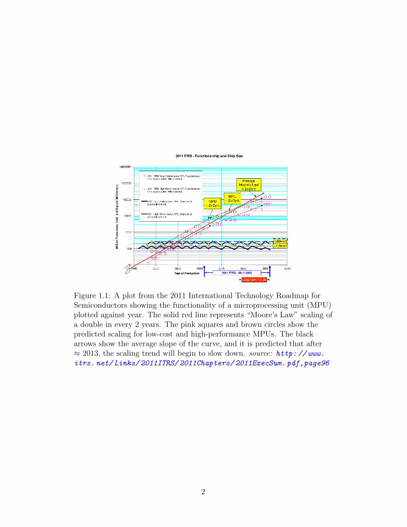
Figure 1.1: A plot from the 2011 International Technology Roadmap forSemiconductors showing the functionality of a microprocessing unit (MPU)plotted against year. The solid red line represents “Moore’s Law” scaling ofa double in every 2 years. The pink squares and brown circles show thepredicted scaling for low-cost and high-performance MPUs. The blackarrows show the average slope of the curve, and it is predicted that after≈ 2013, the scaling trend will begin to slow down. source: http: // www.
itrs. net/ Links/ 2011ITRS/ 2011Chapters/ 2011ExecSum. pdf,page96
2

different physical principles.
Post-CMOS device research has become an incredibly active and diverse
research area with many competing technologies [2]. However, no clear suc-
cessor to silicon CMOS has emerged. In the effort to minimize devices as
much as possible, the field of molecular electronics has gained serious atten-
tion [8]. While molecular electronics can offer extremely high device density
and low-power operation, it currently suffers from issues regarding molecule-
electrode coupling, low yield, and difficulty in making three-terminal devices,
which are the building blocks of logic circuits [8]. In addition to molecular
electronics, the improvement of nano-scale fabrication techniques has resur-
faced interest in using mechanical systems. Logic switches constructed from
nanoelectromechanical systems (NEMS) offer effectively zero leakage cur-
rent and an extremely sharp transition between insulating and conducting
states [9]. However, high-frequency switching speed and reliability remain
challenges for NEMS switches. Compared to these more exotic approaches,
the tunnel field-effect transistor (TFET), whose operation is based on band-
to-band tunneling [7], has shown much recent progress. TFETs showcase a
low off-state current and a subthreshold slope experimentally demonstrated
to be less than 60 mV/dec for carbon nanotube (CNT) TFETs. However,
TFETs are based on tunneling processes, they have a low on-state current
and any CNT based design suffers from the fabrication challenges associated
with CNTs, namely the precise placement of CNTs to build circuits and the
lack of ability to differentiate semiconducting CNTs from metallic ones.
A device that is predicted to showcase extremely low power dissipation
and a subthreshold slope significantly less than 60 mV/dec [10] is a logic
switch based on a room-temperature superfluid exciton condensate in dou-
ble layer graphene [10–13]. The stability of an exciton condensate in double
layer graphene depends on many factors and complex interactions. Previous
theoretical work has examined the effects of screening [14, 15], fluctuations
due to finite-temperature [13], layer scaling [16], and disorder [17, 18]. In
continuing to build on this knowledge, it is important to understand how
transport in such a system is affected by phonon scattering in the individ-
ual graphene layers, as both theoretical and experimental work has shown
that phonons negatively impact the room-temperature transport properties
of graphene [19–21].
3

1.2 Superfluids
As mentioned in the previous section, the device being studied in this thesis
is predicted to achieve ultra-low power operation because of a phase tran-
sition from a normal Fermi-liquid into an excitonic superfluid. Superfluid-
ity is closely related to Bose-Einstein condensation, and both are a conse-
quence of quantum statistics that occur because bosons can occupy the same
single-particle coherent state with a well-defined phase. In the case of a
Bose-Einstein condensate (BEC), a fraction of the particles (known as the
condensate fraction) condense into the ground state of the system.
As an introduction to the concept of Bose-Einstein condensation, one typ-
ically starts with the ideal Bose gas. The Bose-Einstein distribution gives
the statistical distribution of bosons with energy Ei,
Ni =1
e(Ei−µ)/kBT − 1. (1.1)
For a gas of non-interacting bosons with mass m, Ei is simply the energy
for a free particle Ei =hk2i2m
. The density of particles can be obtained by
integrating Eq. (1.1) over all k. When integrated with µ = 0 one obtains the
expression
n =1
V
∑k
Nk =
(1
2π
)3 ∫d3k
1
eβ(h2k2/2m) − 1= 2.612
(mkbT
2πh
)3/2
(1.2)
where V is the volume of the system and β = kb/T .
The integral above did not include the state with k = 0, but multiple
particles are allowed to be in the ground state. When Eq. (1.2) is solved
for T , the critical temperature for the ideal Bose gas to condense into the
ground state is given:
Tc = 1.054πh2n3/2
mkb(1.3)
For superfluids, the particles do not necessarily condense into the zero-
momentum state, but can move with a superfluid velocity [22]. The super-
fluid density gives the density of particles in the superfluid state and the
superfluid density can be treated as the order parameter for the phase tran-
sition: it is non-zero only in the condensed state. A plot of the superfluid
fraction (the superfluid density divided by the total particle density) for the
4

0 1 2 3 4 5 6Temperature (K)
0.0
0.2
0.4
0.6
0.8
1.0
ρs/ρ
Tc
Figure 1.2: The superfluid fraction vs. temperature for 10 non-interactingbosons of mass me in a 50 nm3 periodic simulation cell, obtained frompath-integral Monte Carlo simulations. From Eq. (1.3), Tc ≈ 5.44 and thisvalue is denoted by a dashed vertical line. The simulations were performedusing the open source pi-qmc programhttp://code.google.com/p/pi-qmc/.
ideal Bose gas is given in Fig. 1.2.
Condensed matter physicists have been studying superfluids for many years
and superfluidity was first observed experimentally during the 1930s. When
experimentalists cooled liquid 4He below ∼2.17K, it was discovered that 4He
has essentially infinite heat conductivity (it does not boil as no gas bubbles
are observed in 4He below this temperature) and that it has zero-viscosity (it
can flow through small capillaries without dissipation) [23, 24]. This super-
fluid transition in 4He was initially named the “lambda” transition because
of the shape of the 4He specific heat curve, as shown in Fig. 1.3 [25]. While
many theories were debated for a time, it was eventually settled that this su-
perfluid quantum phase transition is possible because 4He is composed of an
even number of fermions (two electrons, two protons, two neutrons), which
makes the composite particle, 4He, a boson.
Furthermore, it was observed in the 1970s that the 3He isotope also had
phases that exhibited superfluid properties [26]. 3He, however, is composed
of an odd number of fermions and therefore is a fermion itself. The current
accepted theory is that 3He atoms form composite p-wave pairs which then
act as bosons [27]. This pairing is analogous to Cooper pairing in a supercon-
ductor, where electrons can form s-wave pairs due to phonon interactions [28].
The composite 3He pairs have additional internal degrees of freedom because
5

Figure 1.3: One of the first experimental observations of superfluidity was adiscontinuity in the specific heat curve of liquid 4He observed near 2.2 K.Reprinted from Physica, Vol. 2, W.H. Keesom and A.P. Keesom, Newmeasurements on the specific heat of liquid helium, 557-572, Copyright1935, with permission from Elsevier, http://www.elsevier.com.
their total spin S and orbital angular momentum L are 1 (vs. L = S = 0 for4He) and therefore pairs of 3He can have L and S with different projections,
which allows for multiple condensed phases with varying properties [29].
Technological advances within the last 15 years have spurred cold-atom
research and the creation of “optical lattices.” Optical lattices are formed by
interfering laser beams and they allow experimentalists to tailor potentials
within which they can study fundamental physics by recreating systems that
would only occur in crystals and other condensed matter systems. The use of
optical lattices provides a highly-controlled environment where parameters
such as the geometry and height of the potential can be fine-tuned [30]. In
6

particular, the interaction strength between atoms can be set by adjusting the
optical lattice potential. This tuning of an exchange interaction in 87Rb [31]
led to one of the most intriguing results of cold-atom research to date: the
ability to tune 87Rb between a Mott-insulator state (where the atoms are
confined to their lattice sites) and a superfluid state and then back again [32].
1.3 Bose-Einstein Condensation of Excitons
An exciton is a bound electron-hole pair joined by a mutual Coulomb attrac-
tion. Excitons are allowed to condense because the half-spin electrons and
holes combine to form integer-spin bosons. However, an important distinc-
tion between the BCS-style phase transition in superconductors and BEC of
excitons is that condensation of Cooper pairs usually occurs at the onset of
pair formation, where excitons exist in non-condensed phases. BCS states
also form on the edge of the Fermi surface, whereas a BEC of excitons can
form across the entire bandwidth. A BEC of excitons was initially predicted
in the 1960s [33], but has gained recent interest because of experimental
evidence for these condensed phases.
Due to attractive Coulomb interactions, excitons normally have a finite
lifetime before recombining and emitting a photon. Thus, in order to realize
an exciton condensate, the underlying system must be designed to prevent
recombination while still allowing for sufficient interaction so excitons can
form [34].
Excitons can be formed in many semiconductors, and in the 1990s attempts
were made to realize an exciton condensate in materials where recombination
is suppressed, for example due to the underlying symmetries present in Cu2O.
Over the years, many experiments have been done in Cu2O [35–37] as Cu2O
boasts an exciton lifetime of tens of microseconds [35]. However, some the-
ories claim that non-radiative processes such as Auger recombination make
observing a condensate in Cu2O unlikely [38].
A more attractive approach is to spatially separate the constituent quasi-
particles that make up excitons so that extremely long lifetimes could be
achieved [39]. These so-called indirect excitons can be formed in double layer
semiconductor quantum wells by confining electrons to one layer and holes to
other layer, with a dielectric tunnel barrier between the two wells to suppress
7

recombination. Experimental evidence of BEC in coupled quantum wells has
been indicated by the existence of a “dark-spot” in the photoluminescence
pattern of optically generated excitons, where excitons travel long distances
without emitting light. In these quantum well systems, this dark spot has
been attributed as a signature of exciton condensation as it appears only
above a critical density and that decreases with lower temperatures [34,40].
Theoretically, a double layer system that is expected to exhibit an exci-
ton superfluid can be described using a pseudospin formalism [41], where the
layer degree of freedom is mapped on to a spin-1/2 particle. In this formalism,
the top layer is mapped to pseudospin-up | ↑〉 and the bottom layer is mapped
to pseudospin-down | ↓〉. Exciton condensation can then be viewed as pseu-
dospin ferromagnetism, where the quasiparticles are in a superposition of
both layers and the system becomes an XY pseudospin ferromagnet. [13,42].
Some of the most compelling experimental evidence for condensation of
indirect excitons has been observed in coupled wells in the quantum Hall
regime, when electron-electron layers are each tuned to 1/2 filling. In this
case, a particle-hole transformation can be made, and a nearly identical pop-
ulation of electrons and holes can be achieved with each layer as close to 1/2
filling as possible [43,44]. It is worth noting that this particle-hole transform
is equivalent to the typical treatment of holes in the valence band. Figure 1.4
shows an experimentally measured tunneling peak for quantum well systems
with two different layer separations. When the layers are relatively far apart,
tunneling of electrons at low voltages is suppressed by intralayer correlations
because an electron is unable to tunnel into a layer with high magnetic field
without disturbing the collective motion of electrons in that layer. However,
when the layer separation is reduced, a large tunneling peak is observed at
low voltages. This significant difference in tunneling rates at minor changes
in layer separation is attributed to a quantum phase transition. The argu-
ment that this tunneling peak is the mark of a phase transition is further
strengthened by the appreciable reduction of the peak with increased tem-
perature or deviation from a field that gives half filling [45]. While these
tunneling experiments show strong evidence of an exciton condensate, they
do not demonstrate superfluidity directly and transport measurements are
needed to confirm superfluid properties, as condensation does not strictly
require superfluidity.
While the strong evidence pointing to the existence of a superfluid exciton
8

Figure 1.4: Experimental evidence of a phase transition to a Bose-Einsteincondensate of excitons in coupled quantum wells at half filling. The plotshows tunneling rate vs. interlayer voltage. When the layers are separatedat a large distance, interlayer tunneling is minimal (blue line), but when thelayers are sufficiently close enhanced interlayer Coulomb interactions leadto a strong peak in tunneling rate (red line) that is attributed tospontaneous interlayer coherence. Reprinted by permission from MacmillanPublishers Ltd: Nature [43], copyright (2004). http://www.nature.com/
condensate in these quantum Hall systems is certainly exciting, the potential
to exploit these superfluid properties for device use is severely hampered by
the low temperature and strong magnetic field required to drive this phase
transition. In 2008, a theoretical prediction was made for the superfluid
phase transition to occur at or above room temperature (300 K) when two
sheets of graphene were used instead of semiconductor quantum wells [11,12].
Graphene is a favorable material to exhibit a high transition temperature be-
cause of its linear, symmetric bands (which allows for easier balance of elec-
tron and hole populations, in contrast to conventional bulk semiconductors),
strong ambipolar field effect (which allows for a large enough quasiparticle
density to achieve condensation), and it is atomically two-dimensional. The
phase diagram that predicts a room temperature condensate as published in
9

Ref. [11] is shown in Fig. 1.5 and the bandstructure obtained from the mean-
field calculations is shown in Fig. 1.6. As can be observed from the figures,
a strong field effect is critical for condensation, as well as precise tuning of
layer separation.
The bold claim of room-temperature superfluidity is controversial and
other works predict that strong screening of interlayer interactions can de-
crease the predicted transition temperature by orders of magnitude into the
milli-Kelvin regime [14]. This lower transition temperature is predicted be-
cause the authors considered screening from each fermionic degree of freedom
to add independently and the screening in the condensate phase is then essen-
tially the same as in the normal Fermi liquid phase. However, path integral
Monte Carlo simulations show that while the additional fermion flavors do
reduce the transition temperature, the effect of screening is not as drastic
due to strong exciton binding and interlayer correlations [15].
While the transition temperature is a widely debated topic, the dispute
will eventually be settled by experiment and experimentalists are actively
working towards creating double layer graphene systems for this purpose. A
type of experiment that can measure interlayer correlation is a Coulomb drag
experiment. In Coulomb drag experiments, electron and hole populations
are induced in a double layer system in which each of the layers has an
independent set of contacts. A current is then driven in one of the layers and
a voltage is measured in the opposite layer. This measured voltage shows
evidence of a correlated exciton population as holes in one layer are dragged
by the electrons in the other layer. In 2011, Coulomb drag measurements
provided exciting evidence of the interlayer interactions which may lead to the
experimental realization of an exciton condensate in double layer graphene
[46].
10

Figure 1.5: The predicted transition temperature to room excitonsuperfluid plotted against external electric field Eext and layer separation d.Reprinted figure with permission from Hongki Min, Rafi Bistritzer,Jung-Jung Su, and A. H. MacDonald, Physical Review B, 78, 121401(R)(2008). Copyright 2008 by the American Physical Society.http://prb.aps.org/abstract/PRB/v78/i12/e121401
Figure 1.6: The bandstructure obtained from mean-field calculations for adipolar superfluid in double layer graphene, showing the superfluid gap thatis opened when the system condenses into the ground state. Reprintedfigure with permission from Hongki Min, Rafi Bistritzer, Jung-Jung Su, andA. H. MacDonald, Physical Review B, 78, 121401(R) (2008). Copyright2008 by the American Physical Society.http://prb.aps.org/abstract/PRB/v78/i12/e121401
11

1.4 The Device Under Consideration
In this thesis, the effect of phonon scattering is investigated on an exciton
superfluid in double layer graphene. The non-equilibrium Green’s function
formalism is used to perform quantum transport simulations of the device
shown in Fig. 1.7. This device consists of two 30 nm x 10 nm sheets of zig-
zag graphene separated by 1 nm of SiO2 tunnel dielectric. Gates on the top
and bottom of the device are used to adjust the Fermi energy of each layer to
values favorable for room-temperature exciton condensation (the field from
these gate electrodes corresponds to Eext in Fig. 1.5). Each of the layers
are terminated by a separate set of contacts for current to be injected and
extracted. The graphene layers are assumed to be perfectly registered (lattice
site A in the top layer is matched with lattice site A in the bottom layer)
and are considered ideal, i.e. free from defects and disorder.
12

Figure 1.7: Schematic of the device under consideration: two layers ofgraphene separated by 1 nm of dielectric (SiO2). Each layer has a separateset of contacts (VTL and VTR for the top layer and VBL and VBR for thebottom layer) and is gated independently by VTG and VBG to the desiredcarrier concentration.
13

Chapter 2
Graphene
2.1 Transport Properties
Graphene, the atomically 2D honeycomb allotrope of carbon has generated
much research interest because of its astounding material properties [6,47,48].
It is one of the strongest materials known to exist and has incredibly unique
electronic properties. The electronic structure of a single layer of graphite
was first discussed in 1947 [49], but it was originally assumed that one could
not isolate a single atomic layer of carbon, so graphene was dismissed as a
purely theoretical material that would be unstable at room-temperature due
to the thermal fluctuations occurring on the order of the interatomic spacing.
However, in 2004, a research group at the University of Manchester isolated
atomically thin carbon films and observed astonishing electrical properties
in these films such as high carrier mobility and the ability to sustain large
currents [50–52]. After the experimental isolation of atomic layers of carbon,
interest in graphene for use in electronics began to grow. As exciting as the
discovery was, graphene did not gain significant attention from the commu-
nity at large. However, in 2005 it was shown that graphene not only exhibits
a strong ambipolar field effect, but also that it could exhibit Shubnikov-de
Haas oscillations at room temperature. Most importantly, it was shown ex-
perimentally that quasiparticle excitations in graphene could be described
as massless Dirac fermions [53], boosting the interest in graphene for use by
physicists as a playground for testing new phenomena. The linear dispersion
relation and particle-hole symmetry in graphene provide direct experimental
access for testing quantum electrodynamic effects because they behave very
much like Dirac fermions in quantum electrodynamics (QED). Experiments
have demonstrated the QED phenomena of Klein tunneling, where the trans-
mission of an electron through an energy barrier becomes close to unity if
14

the barrier’s height is larger than the electron’s rest energy [54,55].
As mentioned in the previous paragraph, a large part of the interest in
graphene from the physics community can be attributed to the honeycomb
lattice, which gives graphene its unique dispersion relation (see Fig. 2.1).
Near the K and K′ points in the Brillouin zone, low energy quasiparticles in
graphene can be described by the Dirac equation, similar to that of photons,
but with the speed of light c replaced by the Fermi velocity vF ≈ 106 m/s [6]:
E = hvF
√k2x + k2
y (2.1)
Figure 2.1: Honeycomb lattice structure showing a carbon nanotube (a)and a 3D plot of the dispersion relation (b) for graphene. For low energyexcitations near the K and K′ points, the dispersion relation is essentiallysymmetric, gapless, and linear. The dispersion relation in graphene canthen be described by the Dirac equation and is given by Eq. (2.1).Reprinted by permission from Macmillan Publishers Ltd: NatureNanotechnology [6], copyright 2007.http://www.nature.com/nnano/index.html
The semiconductor device community is chiefly interested in graphene be-
cause of the quality of available samples and their extremely high room-
temperature mobility (in excess of 15,000 cm2V−1s−1). These properties
have led researchers to experimentally observe ballistic transport at temper-
atures of 300 K [47]. However, because graphene is gapless and transistors
based on graphene exhibit an on-off ratio of roughly 10 to 100, its eventual
use as a semiconductor device material may very well not be as a field-effect
transistor for logic applications, but possibly for THz transistors in commu-
nications applications [56].
15

2.2 Electron-Phonon Interactions in Graphene
As discussed in the previous section, graphene is famous for having near-
ballistic transport at room temperature. However, this should not be taken
to imply that scattering mechanisms like phonons have no effect on trans-
port in graphene. In 2007, it was shown that graphene does in fact observe
a strong electron-phonon coupling, because phonons in graphene are con-
fined to the 2D crystal and an analogy was drawn to photon-Dirac fermion
interactions (further extending the analogies of graphene to quantum elec-
trodynamics) [57]. The electron-phonon coupling was found to be so strong
that it was concluded that the Born-Oppenheimer approximation (where the
motion of electrons and the lattice are treated separately) is not valid in
graphene. Although this strong electron-phonon interaction led theorists to
believe that graphene could exhibit superconducting properties, it remains to
be shown that intrinsic graphene can demonstrate superconductivity [58,59].
However, density functional calculations demonstrated promise of achiev-
ing superconductivity in graphene by depositing Li adatoms that sit in the
hollow sites in graphene to increase the electron-phonon coupling [60]. It
was demonstrated that the critical temperature of a single layer of LiC6 was
roughly 17 K, compared to the bulk critical temperature of 0.9 K.
Since graphene is atomically two-dimensional, six phonon modes are ex-
pected to exist: an optical and acoustic mode propagating in each of the
transverse (or shear) direction, longitudinal direction, and out of plane. The
phonon dispersion relation for graphene is plotted in Fig. 2.2, including both
results from experiment and density functional calculations. In Fig. 2.2, the
graphene phonon dispersion is essentially flat for longitudinal optical modes
at wave vector near the Γ point q = 0 and low energy and linear for the
longitudinal acoustic modes near Γ. These properties will become important
in simplifying the electron-phonon interaction used in this work.
Acoustic longitudinal phonons couple the strongest with electrons in
graphene, as the out of plane modes couple very weakly with electrons and
the energy cost for optical phonon scattering is often too high for many bias
configurations. In theoretical calculations, electron-acoustic phonon interac-
tions are normally treated within the deformation potential approximation,
where one accounts for phonons by a hydrostatic strain that causes a shift
in the energy bands of a material [22]. Within the deformation potential
16

approximation, acoustic phonons have been demonstrated to limit the room
temperature mobility of graphene nanoribbons [61]. While the deformation
potential approximation is useful for characterizing the electron-phonon in-
teraction, the value of the deformation potential constant Da in the literature
varies from 4.5 eV [21] to 19 eV [20], which can result in an order of magnitude
difference in coupling strength since coupling scales as ∝ D2a (see, for exam-
ple, Eq. (5.29)). Using deformation potential scattering, even within the
simplified self-consistent Born approximation used in this thesis (discussed
more in Section 5.2), it was shown that phonons could have an effect on the
transport of graphene nanoribbon transistors with channels only 30-90 nm
long and 2 nm wide [62].
Much of the work done with graphene on SiO2 shows that remote interface
phonons arising from the polar optical modes in SiO2 can severely degrade
transport in graphene on SiO2 [63,64]. This interaction would be important
for the device under consideration in this thesis, but the theoretical tools
to perform reasonable quantum transport calculations of such an interaction
remain to be developed.
17

Figure 2.2: The phonon dispersion relation for graphene, showing ab initiodensity functional theory calculations (solid lines) and experimental datafrom reflection electron-energy-loss spectroscopy (open squares) andhigh-resolution electron-energy-loss spectroscopy (filled circles). Reprintedfigure with permission from O. Dubay and G. Kresse, Physical Review B,67, 035401 (2003). Copyright 2003 by the American Physical Society.http://prb.aps.org/abstract/PRB/v67/i3/e035401
18

Chapter 3
Transport in a Double Layer GrapheneSuperfluid
3.1 Andreev Reflection
Excitons are charge neutral, but in order for an exciton condensate to be
useful for logic devices, the condensate needs to be able to sustain a current.
This current flow can be obtained using the proper bias schemes if the layers
are individually contacted [65]. In Fig. 3.1, an analogy to Andreev reflection
[66] in a normal metal-superconductor-normal metal junction is made [16].
Figure 3.1(a) shows the process of Andreev reflection. In the superconducting
state, electrons are bound into Cooper pairs and as a result of this pairing,
an energy gap is opened in the excitation spectrum. An electron injected
from one of the contacts with an energy below this gap cannot pass through
the superconducting region because there are no available single electron
states at the specified energy. Instead, a Cooper pair is launched across
the superconductor and a hole is reflected back to the originating metal
contact for conservation of momentum. Similarly, in Fig. 3.1(b), an electron
is incident from the top left contact. As in the case of a superconductor,
a superfluid gap is opened and the electron travels a short distance before
it is reflected off of the superfluid gap and out of the bottom left contact.
To conserve momentum, an exciton is sent across the channel. The bias
geometry (VTL = −VTR and VBL = VBR = 0 V ) used to generate this current
is referred to as the “Drag-Counterflow” scheme [65] and steady-state current
flow is possible when:
ITL + IBL = ITR + IBR (3.1)
In both the superconducting and the exciton condensate cases discussed
above, the injected electron travels a certain distance before being reflected
off of the energy gap. A quantity that will become important in later chapters
is the maximum distance that a quasiparticle will travel before undergoing
19

a reflection event. In the literature, this quantity has been labelled the
coherence length (also commonly referred to as the Josephson length λ) [16]:
Lc ≈1
kf
√ρs
∆sas
(3.2)
kF is the Fermi wavenumber, ρs is the superfluid density, and ∆sas is the sin-
gle particle tunneling energy. Previous studies have shown that even small
amounts of disorder within the coherence length have a severe negative im-
pact on transport in this system [18].
Figure 3.1: Illustration comparing Andreev reflection in a normalmetal-superconductor-normal metal interface and the current injectionprocess in a bilayer exciton condensate. Both the superconductor andexciton superfluid have a gap in their excitation spectrum and transport inthe exciton superfluid can be viewed by analogy to Andreev reflection. In(a), an electron with energy less than the superconducting gap (black) isincident from the left contact. A Cooper pair propagates through thesuperconductor and a hole is reflected to conserve momentum. In a bilayerexciton condensate (b), a similar process occurs, except an electron isincident on the top left contact and then reflected as an electron in thebottom left contact, launching an exciton to conserve momentum. Figureobtained from Ref. 16, c© 2010 IEEE.
20

3.2 Critical Current
The current injection process described previously is stable up to a value
known as the critical current (Ic), the maximum sustainable interlayer cur-
rent before the condensate phase is lost. As Ic determines the operational
constraints of the device, it is the most important parameter in such a sys-
tem and the main purpose of this work is to examine the effect of phonon
scattering on Ic.
The derivation of the critical current is most easily explained in the pseu-
dospin notation [42]. In the pseudospin notation, the condensate magnitude
and phase in the presence of electrical bias potentials are determined by the
dynamic Landau-Lifshitz-Slonczewski (LLS) equation,
0 = −ρsh~∇2φ+
1
2
∆sasn
hsinφ− 1
2~j · ~∇mz (3.3)
where φ is the phase of the order parameter, ∆sas is the single particle tun-
neling energy, n is the pseudospin density, ~j is the pseudospin current, and
mz is the pseudospin projection along the z-axis, where mz=1 (-1) corre-
sponds to a particle in the top (bottom) layer. Inside the region A where mz
is constant (where there is no pseudospin-transfer torque since this region is
far from the contacts), the steady-state solution of the LLS equation must
satisfy an elliptic sine-Gordon equation (obtained by taking ~∇mz = 0 and
substituting for Lc):
L2c~∇2φ− sinφ = 0 (3.4)
where Lc is the coherence length , previously described by Eq. (3.2).
The upper bound on interlayer current is calculated by integrating Eq.
(3.4) over the area over which mz is constant, A:
ρs
∫P
~∇φ · n =ρsA
L2c
sin(φ) (3.5)
The maximum attainable current is found to coincide with an order pa-
rameter phase of π/2, when sinφ = 1. When Lc is less than device length
(the case for the simulated device), the value of ~∇φ · n along the edge of A
near the source contact cannot differ from ~∇φ · n along the edge of A near the
drain contact by more than ∆sasn, due to energy conservation. This allows
A to be replaced by WLc in Eq. (3.4), and yields Eq. (12) in 42 and Eq.
21

(3.6) below:
Ic ∼eWρshLc
, (3.6)
where e is the elementary charge and W is the device width.
22

Chapter 4
Non-Equilibrium Green’s Function Simulations
4.1 Overview
Traditional semiconductor device simulations typically use an approach based
on the Boltzmann transport equation (BTE) [67]. However, the semiclassi-
cal BTE is not appropriate for systems where quantum mechanics play an
important role, as is the case for the system considered in this thesis. As
nanoscale devices become increasingly popular, simulations of these smaller
devices are required to better account for the quantum nature of charge car-
riers observed at the nanometer length scales. While scattering processes
like electron-phonon interactions can be included, pure quantum effects such
as Bose-Einstein condensation simply cannot be modeled by the BTE. As
engineers are growing more and more interested in the quantum nature of
devices, quantum simulation methods are becoming increasingly important.
The method discussed in this chapter is arguably one of the more popular
and powerful methods available today. The non-equilibrium Green’s func-
tion (NEGF) formalism is a Green’s function [68, 69] based approach that
has found wide application in solving transport problems for nanoscale de-
vice simulations [70, 71].
Figure 4.1 illustrates a high-level overview of a device as it is represented
in a NEGF simulation. The device is described by a Hamiltonian matrix, H,
which is the energy operator for the system. In principle, the Hamiltonian
fully describes the entire system, involving all scattering processes and the
full region of the contacts. As this would result in a matrix that would be
computationally intractable, it is more convenient to write only the Hamil-
tonian for the region of the device we are interested in (e.g. the channel in
a MOSFET) and include the effects of the contacts and internal scattering
processes as self-energy matrices, Σ. Once the Hamiltonian and self-energy
23

terms have been defined, we can calculate the retarded Green’s function from
a matrix inversion:
GR(E) =[(E + i0+)I −H − ΣL(E)− ΣR(E)− Σph(E)
]−1(4.1)
where 0+ is a positive infinitesimal and I is the identity matrix. ΣL(E),
ΣR(E), and Σph(E) are the self-energy terms that describe the effects of the
left contact, right contact, and phonon scattering, respectively. The real part
of these self-energies is related to a shift in energy and the imaginary part is
related to the broadening of energy levels. While the quantities in Eq. (4.1)
have only been written as a function of energy E, it is important to note that
they are in fact full complex-valued matrices of the chosen basis. Throughout
this thesis, an atomistic real-space basis (where the atomic orbitals at each
lattice site are used as the basis) is assumed for all NEGF functions.
Figure 4.1: Illustration of a generic device being simulated under NEGF.The region of interest (or “device region”) in the device is represented bythe Hamiltonian H (e.g. the channel in a MOSFET). The device isconnected to the environment via the self-energy terms ΣL, ΣR, and Σph
that describe the left contact, right contact, and phonon scatteringprocesses, respectively.
4.2 Tight-Binding Hamiltonian
The Hamiltonian H describes the electron dynamics in the device region, as
described in the previous section. In this section, a three-dimensional device
which is composed of multiple uniform two-dimensional layers is represented
by a nearest-neighbor tight-binding Hamiltonian. The device being described
24

is Nx x Ny xNz lattice sites in the x, y, and z dimensions. In the atomistic
real-space basis, the tight-binding Hamiltonian takes the form of an Nz x Nz
nested block-tridiagonal matrix:
H3D =
. . . 0. . . . . . . . . 0 . . . . . . . . .
. . . . . . 0 T †z H2D Tz 0 . . . . . .
. . . . . . . . . 0. . . . . . . . . 0 . . .
(4.2)
H2D is the Hamiltonian that describes a single layer and Tz is the hopping
matrix that describes hopping in the z-direction between layers.
Each layer Hamiltonian is itself an Nx x Nx block tridiagonal matrix com-
posed of Ny x Ny blocks:
H2D =
. . . 0. . . . . . . . . 0 . . . . . . . . .
. . . . . . 0 T †x Hy Tx 0 . . . . . .
. . . . . . . . . 0. . . . . . . . . 0 . . .
(4.3)
Tx describes the hopping in the x direction and Hy describes each slice of the
device in the y dimension.
Finally, Hy is a standard nearest neighbor one-dimensional Hamiltonian:
Hy =
. . . 0. . . . . . . . . 0 . . . . . . . . .
. . . . . . 0 t† V t 0 . . . . . .
. . . . . . . . . 0. . . . . . . . . 0 . . .
(4.4)
t describes nearest neighbor hopping and is equal to the hopping energy
if two lattice sites are nearest neighbors and is zero otherwise. V is the
onsite energy, which can be a combination of bias potential, electrostatic
potential, or impurity potentials. In the case of the electrostatic potential,
it is conventional to solve the NEGF equations self-consistently with the
Poisson equation:
∇2V (~r) =e2
ερ (4.5)
where e is the elementary charge, ε is the dielectric constant of the material,
and ρ is the charge density - which is obtained self-consistently from the
NEGF equations (see Section 4.4 for details on how the density is calculated).
25
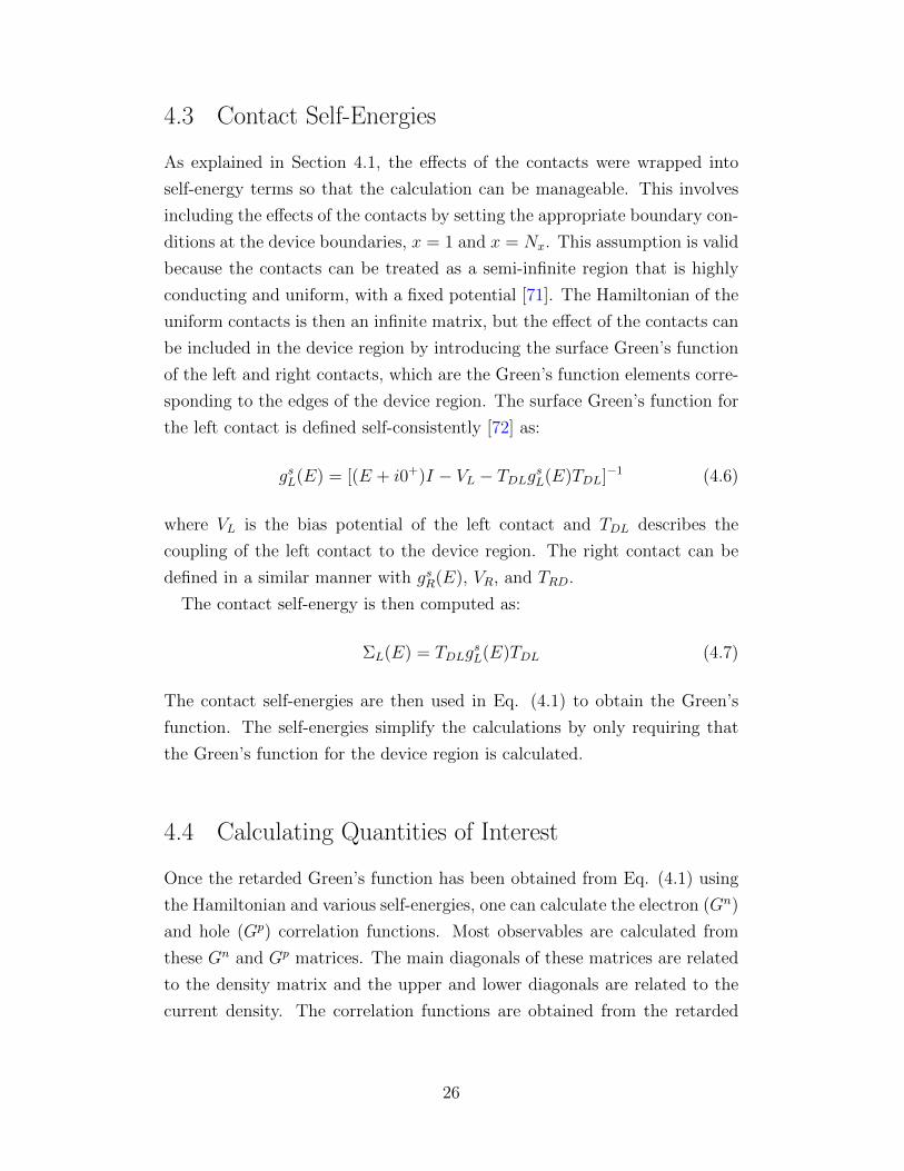
4.3 Contact Self-Energies
As explained in Section 4.1, the effects of the contacts were wrapped into
self-energy terms so that the calculation can be manageable. This involves
including the effects of the contacts by setting the appropriate boundary con-
ditions at the device boundaries, x = 1 and x = Nx. This assumption is valid
because the contacts can be treated as a semi-infinite region that is highly
conducting and uniform, with a fixed potential [71]. The Hamiltonian of the
uniform contacts is then an infinite matrix, but the effect of the contacts can
be included in the device region by introducing the surface Green’s function
of the left and right contacts, which are the Green’s function elements corre-
sponding to the edges of the device region. The surface Green’s function for
the left contact is defined self-consistently [72] as:
gsL(E) = [(E + i0+)I − VL − TDLgsL(E)TDL]−1 (4.6)
where VL is the bias potential of the left contact and TDL describes the
coupling of the left contact to the device region. The right contact can be
defined in a similar manner with gsR(E), VR, and TRD.
The contact self-energy is then computed as:
ΣL(E) = TDLgsL(E)TDL (4.7)
The contact self-energies are then used in Eq. (4.1) to obtain the Green’s
function. The self-energies simplify the calculations by only requiring that
the Green’s function for the device region is calculated.
4.4 Calculating Quantities of Interest
Once the retarded Green’s function has been obtained from Eq. (4.1) using
the Hamiltonian and various self-energies, one can calculate the electron (Gn)
and hole (Gp) correlation functions. Most observables are calculated from
these Gn and Gp matrices. The main diagonals of these matrices are related
to the density matrix and the upper and lower diagonals are related to the
current density. The correlation functions are obtained from the retarded
26

Green’s function and the in/out scattering functions, Σin and Σout:
Gn/p = GRΣin/out[GR]† (4.8)
i(GR − [GR]†) = Gn +Gp (4.9)
[GR]† is the Hermitian conjugate of GR. Σin and Σout are related to the
imaginary part of the self-energy and represent the rate at which electrons
scatter in/out of the given region.
The imaginary part of the self-energy itself can be defined in terms of the
level broadening, Γ(E) (which corresponds to the broadening of energy levels
due to a scattering mechanism), and the in/out scattering functions which
correspond to the rate at which electrons scatter in and out of a particular
point:
Im(Σ(E)) = −Γ(E)
2= −1
2
[Σin(E) + Σout(E)
](4.10)
The real part and imaginary part of the self-energy are Hilbert transform
pairs, so once the imaginary part has been determined, one can also find the
real part from the Kramers-Kronig relation:
Re(Σ(E)) = PV
∫dE′
Γ(E ′)
2π(E − E ′) (4.11)
where PV stands for the Cauchy principal value.
One is often interested in carrier density, especially when self-consistently
solving the Poisson equation, Eq. (4.5). The electron (n) and hole (p)
density matrices can be obtained from the respective correlation function
by an energy integration:
ρn/p =1
2π
∫Gn/p(E)dE (4.12)
The current flowing at each of the contacts can be calculated as:
IL/R =q
h
∫tr[GpL/R(E)Σin
L/R −GnL/R(E)Σout
L/R
]dE (4.13)
where q is the elementary charge, h is Planck’s constant, and “tr” signifies a
matrix trace.
In the case of contact self energies, the in/out scattering functions are
27

related to the level broadening and Fermi function at the contacts:
ΣinL/R =Γ(E)fL/R(E) (4.14)
ΣoutL/R =Γ(E)[1− fL/R(E)] (4.15)
fL/R is the Fermi-Dirac distribution for either the left or right contact:
fL/R(E) =1
e(E−µL/R)/kBT + 1(4.16)
µL/R corresponds to the chemical potential of the respective contact.
4.5 Recursive Green’s Function Algorithm
Most of the time during NEGF simulations is spent solving Eq. 4.1, which
needs to be obtained for each energy value. Calculating GR requires taking
a matrix inverse, which is a notoriously expensive computational operation.
While the initial matrix may start out as block-tridiagonal, the inverted ma-
trix would be a full matrix. If one were required to compute this full inverse,
the set of problems that could be solved using NEGF would be limited not
only by the time required for computation, but by memory requirements to
store the full matrix representing the Green’s function, electron/hole correla-
tion functions, and buffers to perform the calculations. However, as explained
in Section 4.4, only the diagonal and first off-diagonal elements are necessary
when calculating any observable quantities that one wishes to obtain from
NEGF simulations. Thus, recursive algorithms have been developed to cal-
culate GR [73] and Gn/p [74] without requiring the full matrix inversion [71].
In the outline of the algorithm below, the notation Ai,j corresponds to
the block i, j of the matrix that is to be inverted (that is, the value inside
the brackets on the right-hand-side of Eq. (4.1)) and GRi,j corresponds to
the i, j block of GR. When solving for the Green’s function, the algorithm
iterates starting from the left of the matrix and then back from the right side,
introducing the concept of the left-connected and right-connected Green’s
functions, denoted by gL and gR (typically, gR is not stored unless further
off-diagonal elements are required).
The recursive algorithm to calculate the main diagonal and first off-diagonals
28

of GR, assuming a matrix of N x N blocks is:
1. Begin by calculating gL1,1 = [A1,1]−1
2. For q = 2..N :, calculate: gLq,q =[Aq,q − Aq,q−1g
Lq−1,q−1Aq−1,q
]−1
3. Now GRN,N = gLN,N
4. For q = N..2, calculate:
(a) GRq,q−1 = −GR
q,qAq,q−1gLq−1,q−1
(b) GRq−1,q = −gLq,qAq−1,qG
Rq,q
(c) GRq−1,q−1 = gLq−1,q−1 + gLq−1,q−1Aq−1,qG
Rq,q−1
5. If desired, [GR]† can be calculated and stored during this step to take
advantage of CPU cache locality
The recursive algorithm to calculate the main diagonal and first off-diagonals
of Gn is similar except instead of a matrix inversion, we are replacing Eq.
(4.8). In the case of only contact self-energies, it is likely more desirable
to just calculate the diagonals and first off-diagonals of Gn/p exactly, since
Σin/out will be 0 except for the first and last blocks (this does involve obtaining
additional off-diagonal components to complete the matrix multiplication,
however). When phonon scattering is involved, then Σin/out are non-zero on
the entire diagonal and the matrix multiplication becomes very costly. The
second multiplication would require a full matrix to be stored and used, even
if only the diagonal and first off-diagonal components are desired. Again, as-
suming a matrix of N x N blocks and using gnL to denote the left-connected
Gn (this algorithm also reuses the left-connected Green’s function from the
calculation of GR):
1. Calculate: gnL1,1 = gL1,1Σin1,1[gL1,1]†
2. For q = 2..N , calculate: gnLq,q = gLq,q{
Σinq,q + Aq,q−1g
nLq−1,q−1[Aq,q−1]†
} [gLq,q]†
3. Now GnN,N = gnLN,N
4. For q = N..2, calculate:
(a) Gnq−1,q−1 = gnLq−1,q−1 + gLq−1,q−1
(Aq−1,qG
nq,q[Aq,q−1]†
) [gLq−1,q−1
]†−(gnLq−1,q−1Aq−1,q
[GRq,q−1
]†+GR
q−1,qAq,q−1gnLq−1,q−1
)29

(b) Gnq,q−1 = −
[GRq,qAq,q−1g
nLq−1,q−1 +Gn
q,q (Aq,q−1)†(gLq−1,q−1
)†](c) Use the Hermitian property ofGn to calculate the other off-diagonal:
Gnq−1,q = [Gn
q,q−1]†
The calculation can then be repeated using Σout instead of Σin to obtain Gp.
It is also possible that the relationship between GR and Gn/p outlined in Eq.
(4.9) could be used, but this increases the systematic error already present
in the calculations.
30
Chapter 5
Electron-Phonon Interactions in NEGF
5.1 Phonons
Phonons are quantized lattice vibrations that occur in periodic materials like
crystals. They can be viewed as collective excitations or quantum mechani-
cally as non-interacting bosons. As described in Section 2.2, electron-phonon
interactions can cause the energy bands of a solid to change via a deformation
potential. These interactions can cause electrons to scatter and lose energy
or change momentum. Electron-phonon interactions can also cause electrons
to become correlated and provide for the mechanism behind Cooper pairing
in the BCS theory of superconductivity [28].
As a brief introduction to the quantum mechanical concept of phonons, a
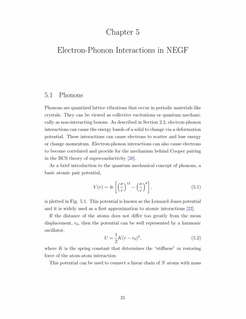
basic atomic pair potential,
V (r) = 4ε
[(σr
)12
−(σr
)6], (5.1)
is plotted in Fig. 5.1. This potential is known as the Lennard-Jones potential
and it is widely used as a first approximation to atomic interactions [22].
If the distance of the atoms does not differ too greatly from the mean
displacement, r0, then the potential can be well represented by a harmonic
oscillator,
U =1
2K(r − r0)2, (5.2)
where K is the spring constant that determines the “stiffness” or restoring
force of the atom-atom interaction.
This potential can be used to connect a linear chain of N atoms with mass
31

0.0 0.5 1.0 1.5 2.0 2.5 3.0r0
r
1.0
0.5
0.0
0.5
1.0
V(r
)
Figure 5.1: A plot of the Lennard-Jones atomic pair potential, Eq. (5.1).Near the minimum, r0, the potential can be approximated as harmonic.
m and including the kinetic term, the Hamiltonian becomes:
H =∑n
[p2n
2m+
1
2K(xn − xn−1)2
](5.3)
where pn is the momentum of the nth atom.
The classical solution of the linear chain problem yields a wave equation
for the position of the nth atom at time t:
xn = x0ei(qan−ωqt) (5.4)
where a is the lattice constant and ωq is the classical eigenfrequency:
ωq = ω0 sin(qa/2) (5.5)
with ω0 as the natural frequency of vibration,
ω0 = 2√K/m. (5.6)
A discrete Fourier transform is performed on xn and pn to give the normal
32
variables:
xq =1√N
∑n
xne−iqan (5.7)
pq =1√N
∑n
pne−iqan (5.8)
These normal variables can be substituted into the original Hamiltonian
and the Hamiltonian can be rewritten by using periodic boundary conditions
(xN = x1) and expanding the sum in Eq. (5.3) (see Ref. 22 pp. 184-185 for
details) as:
H =∑q
[ |pq|22m
+1
2mω2
q |xq|2]
(5.9)
As with the usual “ladder operator” treatment of the simple harmonic
oscillator problem in quantum mechanics [75], the following operators are
defined:
xq =
√mωqh
xq
pq =
√1
mhωqpq (5.10)
b†q =
√1
2(xq + ipq)
bq =
√1
2(x†q − ip†q)
(5.11)
The Hamiltonian in Eq. (5.9) can then be viewed as a sum of independent
simple harmonic oscillator potentials, and using the operators defined above
it can be rewritten as:
H =∑q
(b†qbq +
1
2
)hωq. (5.12)
The Hamiltonian can be understood as a sum of quantized modes q with
energy hωq. The b†q operator (“creation operator”) adds a phonon with
wavenumber q and the bq operator (“annihilation operator”) removes a phonon
33

with wavenumber q.
When treated within the formalism of second quantization, phonon cre-
ation and annihilation operators obey the boson commutation relations:
[bq, b†q′ ] = δq,q′ (5.13)
[bq, bq′ ] = 0 (5.14)
[b†q, b†q′ ] = 0 (5.15)
The number operator b†qbq gives the number of phonons in mode q and
provides expectation values that will be useful when describing the electron-
phonon interaction:
〈b†qbq′〉 = Nqδq,q′
〈bq′b†q〉 = (Nq + 1)δq,q′ (5.16)
where Nq is the Bose-Einstein distribution, Eq. (1.1) with Ei = hωq.
5.2 Self-Consistent Born Approximation
In NEGF device simulations, the contribution from phonon scattering is often
treated with a perturbation theory approach and the phonon self-energies can
be calculated within the self-consistent Born approximation (SCBA) [68,69,
76].
The SCBA can be outlined diagrammatically [69]. The first order per-
turbation to the electron-phonon self-energy has an odd number of phonon
operators, so its expectation value is zero. To lowest (second) order, the con-
tribution from phonon scattering involves a series of “one-phonon” diagrams,
where a free electron (single solid line with arrow) emits a phonon (dashed
curved line), propagates for some time, and the phonon is then reabsorbed
by the same electron. An example of such a diagram is shown in Fig. 5.2.
The Born approximation (BA) is made when one sums up all the contri-
butions of these one-phonon interaction diagrams. The summation neglects
all other higher-order contributions from phonon scattering. The summa-
tion of all these phonon scattering events results in the full Green’s function,
represented by the double line in Fig. 5.3.
34

The self-consistent Born approximation is made by replacing the free elec-
tron Green’s function with the full Green’s function and solving for the in-
teraction self-consistently. The typical diagrams representing the BA and
SCBA are illustrated in Fig. 5.4. In NEGF, many scattering self energies
can be obtained by starting with the expression:
Σin/out(r1, t1; r2, t2) = Dn/p(r1, t1; r2, t2)Gn/p(r1, t1; r2, t2) (5.17)
and this expression is valid for the single-phonon approximation, whereDn/p
is the phonon Green’s function [77].
Figure 5.2: An example single phonon diagram. A free electron withmomentum k emits a phonon with momentum q, which is later reabsorbedby the same electron.
Figure 5.3: The Born approximation is made by summing up allcontributions of one-phonon scattering processes.
5.3 Calculation of the In/Out Scattering Functions
An outline of the calculation of the electron-phonon in/out scattering func-
tions, which will be used to calculate the electron-phonon self-energy terms,
will be given here [69, 76]. In the self-consistent Born approximation, the
35
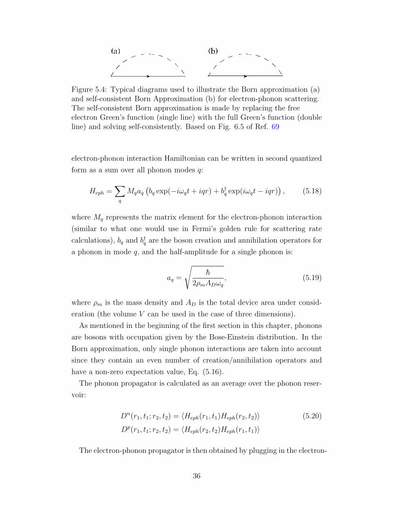
Figure 5.4: Typical diagrams used to illustrate the Born approximation (a)and self-consistent Born Approximation (b) for electron-phonon scattering.The self-consistent Born approximation is made by replacing the freeelectron Green’s function (single line) with the full Green’s function (doubleline) and solving self-consistently. Based on Fig. 6.5 of Ref. 69
electron-phonon interaction Hamiltonian can be written in second quantized
form as a sum over all phonon modes q:
Heph =∑q
Mqaq(bq exp(−iωqt+ iqr) + b†q exp(iωqt− iqr)
), (5.18)
where Mq represents the matrix element for the electron-phonon interaction
(similar to what one would use in Fermi’s golden rule for scattering rate
calculations), bq and b†q are the boson creation and annihilation operators for
a phonon in mode q, and the half-amplitude for a single phonon is:
aq =
√h
2ρmADωq, (5.19)
where ρm is the mass density and AD is the total device area under consid-
eration (the volume V can be used in the case of three dimensions).
As mentioned in the beginning of the first section in this chapter, phonons
are bosons with occupation given by the Bose-Einstein distribution. In the
Born approximation, only single phonon interactions are taken into account
since they contain an even number of creation/annihilation operators and
have a non-zero expectation value, Eq. (5.16).
The phonon propagator is calculated as an average over the phonon reser-
voir:
Dn(r1, t1; r2, t2) = 〈Heph(r1, t1)Heph(r2, t2)〉 (5.20)
Dp(r1, t1; r2, t2) = 〈Heph(r2, t2)Heph(r1, t1)〉
The electron-phonon propagator is then obtained by plugging in the electron-
36
phonon Hamiltonian, Eq. (5.18), into the above equation and using the
Bose-Einstein distribution and the expectation values in Eq. (5.16):
Dn(r1, t1; r2, t2) =∑q
|Mq|2a2q
{(Nq + 1) exp[iωq(t2 − t1) + iq(r1 − r2)] +Nq exp[iωq(t1 − t2) + iq(r2 − r1)]} .(5.21)
This function is then Fourier transformed from the time domain into the
energy domain to give the general energy-dependent phonon in/out scattering
functions:
Σinph(r1, r2, E) = D(r1, r2, E)(Nq + 1)Gn(r1, r2, E + hωq)
+ D(r1, r2, E)∗NqGn(r1, r2, E − hωq)
(5.22)
Σoutph (r1, r2, E) = D(r1, r2, E)∗NqG
p(r1, r2, E + hωq)
+ D(r1, r2, E)(Nq + 1)Gp(r1, r2, E − hωq)(5.23)
where the ∗ operator denotes complex conjugate. Note that in a departure
from the usual notation used in this thesis, the in/out scattering functions
and electron/hole correlation functions have been left as a function of grid co-
ordinates since the phonon coupling operator is still a function of coordinates
r1, r2:
D(r1, r2, E) =∑q
|Mq|2a2q exp[iq(r1 − r2)]. (5.24)
5.4 Calculation of the Acoustic and Optical Phonon
Self-Energies
Up until now, the phonon self-energy has been treated as a single entity,
Σph. However, in graphene there will be a contribution from both acoustic
and optical phonon modes [78], and the self-energy will be a sum of the two
contributions Σph = Σac + Σop. In this study, only the relevant longitudi-
nal phonon modes were included, as the transverse and out-of-plane modes
couple too weakly with electrons in graphene [20]. As will be demonstrated
37
shortly, the phonon self-energies are diagonal in the real-space basis cho-
sen [76], thus simplifying the calculations by allowing for use of the recursive
algorithms for calculation of GR and Gn (see Section 4.5). The basis for this
section is the derivation and results presented in Ref. [76].
As is conventional in NEGF treatments of phonon scattering [62,71,76], de-
formation potential scattering by low-energy acoustic phonons is treated as a
completely elastic process, as the energy of acoustic phonons is much smaller
than the energy scales being considered. The acoustic phonon occupation
number for these low energy modes is extremely high since hωq ≈ 0 � kbT
and Nq ≈ kbThωq
for small hωq. Since Nq � 1, a substitution is then made for
Nq ≈ Nq + 1 ≈ kbThωq
in Eq. (5.22):
ΣinAC(r1, r2, E) =
∑q
|Mq|2a2q exp[iq(r1 − r2)]
kbT
hωqGn(r1, r2, E) + c.c. (5.25)
In the equation above, only the term for phonon emission is included, since
the term for phonon absorption is just the complex conjugate (c.c.) of the
emission term.
Since Nq is extremely large for the low energy modes, the assumption of
elastic scattering is valid. One can then substitute the low energy linear
dispersion relation for acoustic phonons (see Fig. 2.2) ωq ≈ vsq and |Mq| ≈Daq into Eq. (5.22), where vs is the velocity of sound in the material. After
making these substitutions and expanding aq by Eq. (5.19), the following
expression is obtained:
ΣinAC(r1, r2, E) =
∑q
exp[iq(r1 − r2)]D2akBT
2ρmADv2s
Gn(r1, r2, E) + c.c. (5.26)
It should be noted that now the coupling parameter is a constant, indepen-
dent of phonon mode q.
Now, by converting the sum to an integral and using the relation δ(x) =1
2π
∫∞∞ exp(iqx), it is found that the in/out scattering functions are diagonal
in the coordinate space:
ΣinAC(r1, r2, E) =
D2akBT
ρmAv2s
Gn(r1, r2, E)δ(r1 − r2) (5.27)
Where A is now the area of the unit cell, from the normalization of the
38

sum. Also note that the emission and absorption terms have been summed,
resulting in the loss of a factor of 2 from the denominator of Eq. (5.26).
Thus, the in and out scattering functions and electron-phonon self energy
are given as (with the coordinates suppressed again):
ΣAC(E) = KACGR(E)
ΣinAC(E) = KACG
n(E)
ΣoutAC(E) = KACG
p(E)
(5.28)
The acoustic phonon coupling constant KAC contains the constants left
over from the substitutions made by assuming elastic scattering by low-
energy acoustic phonons:
KAC =D2akBT
ρmv2sA
(5.29)
When considering optical phonon scattering, the energy for optical phonons
is often too large to make a similar elastic scattering approximation. For ex-
ample, the optical phonon energy in graphene at q = 0 is hω0 ≈ 164 meV [21].
This results in a coupling between different energy values during the sim-
ulation (E ± hω) which complicates the calculations since NEGF calcula-
tion is traditionally data-parallel across energy values. The problem can be
somewhat simplified by only considering optical phonons of constant energy
near the center of the Brillouin zone [76] and substituting |Mq| ≈ Do and
hωq ≈ hω0 into Eqs. (5.22) and (5.23). In a similar process as outlined
above for acoustic phonon in/out scattering functions, the in/out scattering
functions are then defined as:
ΣinOP (E) = KOP{(N0 + 1)Gn(E + hω0)
+(N0)Gn(E − hω0)}ΣoutOP (E) = KOP{(N0)Gp(E + hω0)
+(N0 + 1)Gp(E − hω0)}
(5.30)
As with earlier functions, the first term in each of the scattering functions
corresponds to the emission of a phonon and the second term corresponds
to the absorption of a phonon. N0 is the occupation number of the optical
phonon mode q = 0 and can no longer be assumed to be dominated by one
term, so it is calculated from the Bose-Einstein distribution, Eq. (1.1). KOP
39

is a coupling constant obtained from the substitutions mentioned above:
KOP =hD2
o
2ρmω0A(5.31)
Once the optical phonon in/out scattering functions have been obtained,
one can calculate the imaginary part of the self-energy via Eq. (4.10) and
then obtain the real part via the Hilbert transform in Eq. (4.11). Note that
including optical phonon scattering imposes a significant burden on memory
and computational effort because Eq. (4.11) requires an energy integration
over the energy axis at each energy value, but most significantly because of
the energy coupling from inelastic scattering. This coupling requires one to
store and transmit (in the case of an MPI implementation) the additional
values Gn/p at energies other than the current value of E in the calculation.
Usually, one just performs the integrals Eq. (4.13) and Eq. (4.12) on the
fly, and the values of Gn/p would be discarded after the calculations are
performed at each energy.
40

Chapter 6
Electron-Phonon Interactions in Double LayerGraphene Superfluids
6.1 Simulation Methodology
The device shown in Figure 1.7 was simulated using the NEGF formalism,
both with and without phonon interactions included. An ideal phenomeno-
logical model for a generic metal contact was used for the contacts that
terminate each layer [72]. This model does not account for any unintentional
doping of the graphene layers that may occur [79]. The nearest-neighbor
tight-binding Hamiltonian used for the top (electron) layer is:
HTL =∑i,j
τTL|i〉〈j|+ Vi|i〉〈i|, (6.1)
where i and j are lattice points of first nearest neighbors, τ = -3.03eV is the
hopping energy for the pz orbital in graphene (which gives the linear disper-
sion relation near the K and K′ points), and Vi is the on-site electrostatic
potential calculated by the three-dimensional Poisson solver, Eq. (4.5). The
bottom (hole) layer is similarly described by HBL, which is the same as HTL
except with τBL = −τTL.
The full device Hamiltonian is a combination of the two layer Hamiltonians
with the interlayer interaction terms:
H =
[HTL 0
0 HBL
]+∑
µ=x,y,z
µ · ~∆⊗ σµ. (6.2)
The interlayer interactions include both single particle tunneling and the
mean-field many-body contribution, ~∆, which couples the two layers using
a local density approximation and drives the phase transition [13]. In Eq.
(6.7), µ represents a vector that isolates each of the Cartesian components of
the pairing vector, and σµ represents the Pauli spin matrices in each of the
41

three spatial directions.
In order to further describe the interlayer interactions, the single particle
density matrix (which can be calculated using Eq. (4.12)) is introduced as:
ρ =
[ρ↑↑ ρ↑↓
ρ↓↑ ρ↓↓
](6.3)
where ↑ and ↓ represent the top and bottom layer such that the on-diagonal
components correspond to the quasiparticle densities of the top and bot-
tom layer. The off-diagonal components of Eq. (6.3) are used to calculate~∆ as well as the order parameter of the phase transition. The directional
components of the psuedospin field are calculated as:
mxexc = ρ↑↓ + ρ↓↑ = 2Re(ρ↑↓)
myexc = −iρ↑↓ + iρ↓↑ = 2Im(ρ↑↓)
(6.4)
As described in Section 1.2, the superfluid density is a good order param-
eter for this type of system and its magnitude can be calculated from the x
and y components of pseudospin fields as [18]:
ρs =√
(mxexc)
2 + (myexc)2. (6.5)
The order parameter phase is also defined as:
φ = tan−1
(myexc
mxexc
). (6.6)
As shown in Eq. (3.5), the maximum interlayer current is obtained when
φ = π/2.
With the mean field contribution defined, the full system Hamiltonian with
interlayer interactions can now be expanded:
H =
[HTL + ∆z ∆x − i∆y
∆x + i∆y HBL −∆z
]. (6.7)
The directional components of the interlayer interaction can be written in
42

GR, Gn/p
Σph
Gn
Vi,∆
ρ
Figure 6.1: Simplified illustration of the self-consistent procedure usedduring the simulations. The phonon self-energies are calculatedself-consistently with GR until Gn is converged. These Gn/p matrices arethen used to calculate the density matrix which is used to calculation theinterlayer interactions and electrostatics. The procedure is repeated untilconvergence of the off-diagonal components of the density matrix isattained.
terms of Eq. (6.4):
∆x = (∆sas + Umxexc) ∆y = Umy
exc
∆z = 12(V↑|i〉〈i| − V↓|i〉〈i|)
(6.8)
where ∆z represents the unbound carriers in each layer, which have a screen-
ing effect. U is the strength of the interlayer on-site Coulomb interaction,
which is fixed at 2.0 eV to account for effects from screening [18,80]. ∆sas is
the single particle tunneling energy, which is fixed at 1 µeV to allow for suffi-
cient exciton lifetime for condensation and convergence of the self-consistent
calculations [18].
The transport quantities are calculated self-consistently with the interlayer
interactions and the electrostatics. A modified Broyden method is utilized
to accelerate convergence of the off-diagonal components of the density ma-
trix [81]. The phonon interaction self-energy terms depend on Gn/p as shown
in Eq. (5.28) and (5.30), adding complexity to the self-consistent calcula-
tions and greatly increasing run time when compared to ballistic simulations
(changing the run time for some simulations from hours to days when optical
phonons are included). The self-consistent procedure used is illustrated in
Fig. 6.1.
43

The self-energy terms for both elastic acoustic phonon scattering (with
deformation potential Da = 19 eV, to account for the largest used value) [20]
and inelastic optical phonon scattering processes (with optical deformation
potential Do = 1x10⁹ eV/cm and energy hω0 = 164.6 meV) [21] are included.
Both interband and intraband scattering are accounted for by utilizing an
atomistic real-space basis [62]. The system temperature is set to Tsys = 300 K
for all calculations.
6.2 Results
The critical current (Ic), as introduced in Section 3.2, is the most impor-
tant device parameter as it determines the operational regime for the device.
The critical current in the simulations is defined as the maximum interlayer
current attained before self-consistency is lost. After the system passes the
interlayer voltage corresponding to the critical current, the interlayer current
drops sharply as the system can no longer sustain the condensate phase and
interlayer tunneling becomes dominated by single particle tunneling [13,18].
While the condensate may persist beyond the critical current, this cannot be
accurately modeled by the steady-state simulations performed in this work
because the solution becomes time-dependent [18,42].
In order to most effectively drive the interlayer condensate current, the bias
voltages are applied in the drag-counterflow configuration [65] in which pos-
itive interlayer voltage is applied to the top left contact (VTL) and an equal
negative interlayer bias is applied to the top right contact (VTR) while the
contacts in the bottom layer remain grounded (VBL = VBR = 0 V ). In these
simulations, the interlayer current is the current measured flowing into the
top left contact and out of the bottom left contact. Since the bottom layer
is grounded, the interlayer current is induced solely by the electron-hole in-
terlayer interactions. The interlayer current-voltage characteristic calculated
for three values of gate voltage (simulated by using three different values of
the layer Fermi energy) is plotted in Fig. 6.2. In Fig. 6.2, |EF | refers to the
magnitude of the layer Fermi energy in each simulation where the top layer
has a Fermi energy of EF and the bottom layer has a Fermi energy −EF .
First, the critical current for a device with a Fermi energy of |EF | = 0.40 eV
is examined. This value was chosen in Ref. [18] to place the system well within
44

Figure 6.2: I-V curves showing the differences observed in interlayertransport with decreasing gate voltage, with and without phononscattering. In the above plots, (a) |EF | = 0.4 eV, (b) |EF | = 0.3 eV, and(c) |EF | = 0.2 eV.
the predicted regime for room-temperature superfluidity, based on the phase
diagram included in Fig. 1.5 with Eext=0.8 V/nm and d=1 nm. The critical
current for the ballistic case is found to be Ic ≈ 18.4 µA, in good agreement
with the analytic value of IAc ≈ 19.5 µA, based on Eq. (3.6), while when
phonons are included Iphc ≈ 17.9 µA representing a change of only 2.7%.
From these results, it would appear as though phonons do not have an effect
on the transport of this device.
In order to investigate the seemingly negligible effect of phonon scattering,
the Fermi levels of the graphene layers were adjusted. At |EF | = 0.30 eV, in
the ballistic case Ic ≈ 13.5 µA and Iphc ≈ 9.2 µA when phonon interactions
are included, representing a 31.9% drop in critical current. These values are
to be compared with the results at |EF | = 0.20 eV, where a critical current
of Ic ≈ 10.0 µA is found for the ballistic case and Iphc ≈ 3.4 µA when phonon
interactions are included, corresponding to a 66.0% drop in critical current.
The variation of the critical current considering both the ballistic and
phonon interaction cases is summarized in Fig. 6.3 by plotting Ic for |EF |from 0.20 eV to 0.40 eV. This region was explored because Fermi energies
below 0.20 eV are far outside of the predicted regime for room-temperature
condensation (even with the most optimistic estimates) and values above
0.40 eV require fields approaching the dielectric breakdown potential of SiO2.
As expected, the critical current in the ballistic case decreases linearly with
Fermi energy due to graphene’s linear bands. A convenient explanation for
this drop is to simply consider the change in Lc as the Fermi energy is de-
creased. In this case, it is expected that the critical current has an inverse
linear relationship with the coherence length [13] from Eqs. (3.6) and (3.2).
45

Simple changes in the coherence length, however, are insufficient to explain
the observed drop in critical current with decreasing |EF | seen when phonon
interactions are included in the simulations. While it is true that Ic does de-
crease linearly with decreasing |EF | in the ballistic case, this is untrue when
phonon interactions are considered as the effect is much stronger. To explain
the non-linear drop in critical current seen when phonon interactions are in-
cluded, the average self-consistent value of the order parameter ρs normalized
to ρs at |EF | = 0.4 eV is plotted with and without phonon interactions in
Fig. 6.4. For the ballistic case, ρs remains close to unity, deviating at lower
|EF | due to confinement effects. This occurs because the Fermi wavelength
is on the order of or larger than the device width at those values, resulting
in a poorly formed Fermi surface. Nevertheless, when phonons are included,
ρs drops quickly as |EF | decreases. This is due to the fact that quasiparticles
can travel farther into the device before being retroreflected, allowing them
to interact more strongly with the phonons in the individual graphene layers.
The energy changes in the carriers attributed to these scattering events serve
to energetically separate the excitons, prematurely breaking interlayer coher-
ence and leading to a large drop in the value of ρs and the corresponding
drop in Ic as |EF | decreases.
46

0.20 0.25 0.30 0.35 0.40Fermi Energy (eV)
0
5
10
15
20
Cri
tica
lCur
rent
(µA
)
BallisticPhonon
Figure 6.3: The value of the critical current (Ic) found at different values ofthe Fermi energy (|EF |) for both the ballistic case (black) and the phononlimited case (red).
0.20 0.25 0.30 0.35 0.40Fermi Energy (eV)
0.0
0.2
0.4
0.6
0.8
1.0
ρs/ρs(|E
F|=
0.4e
V)
BallisticPhonon
Figure 6.4: Plot of the average self-consistent value of the superfluid densityρs normalized to ρs at |EF | = 0.40 eV with and without phononinteractions.
47

Chapter 7
Summary and Discussion
A room temperature exciton superfluid in double layer graphene would not
only be a revolutionary development for the physics community, but it could
also help solve many challenges that device engineers will be facing in the near
future. With this device pending experimental verification, it is important
to understand the room-temperature transport properties of such a system.
In working towards building a theoretical understanding of these devices,
quantum transport simulations have been used to study the impact of carrier-
phonon scattering on transport in a superfluid in double layer graphene. The
effect of carrier-phonon scattering depends strongly on the value of the coher-
ence length of the system. At short coherence lengths, which occur at high
gate voltages, the critical current is not impacted by the presence of phonon
interactions. However, at lower gate voltages corresponding to longer coher-
ence lengths, the critical current is significantly reduced by the presence of
phonon interactions. In addition to the requirement for a relatively large
gate voltage to drive the high-temperature phase transition, phonon scatter-
ing places limits on the operational gate voltages which should be used in
conjunction with these devices to achieve maximum device performance.
48

References
[1] G. E. Moore, “Cramming more components onto integrated circuits,(reprinted from Electronics, vol. 38, no. 8, April 19, 1965, pp.114 ff.),”IEEE Solid-State Circuits Newsletter, vol. 20, no. 3, pp. 33–35, Sep. 2006.[Online]. Available: http://dx.doi.org/10.1109/N-SSC.2006.4785860
[2] K. Bernstein, R. K. Cavin, W. Porod, A. Seabaugh, and J. Welser,“Device and architecture outlook for beyond CMOS switches,”Proceedings of the IEEE, vol. 98, no. 12, pp. 2169–2184, Dec. 2010.[Online]. Available: http://dx.doi.org/10.1109/JPROC.2010.2066530
[3] B. S. Doyle, S. Datta, M. Doczy, S. Hareland, B. Jin, J. Kavalieros,T. Linton, A. Murthy, R. Rios, and R. Chau, “High performancefully-depleted tri-gate CMOS transistors,” IEEE Electron DeviceLetters, vol. 24, no. 4, pp. 263–265, Apr. 2003. [Online]. Available:http://dx.doi.org/10.1109/LED.2003.810888
[4] R. Chau, S. Datta, M. Doczy, B. Doyle, J. Kavalieros, and M. Metz,“High-/metal-gate stack and its MOSFET characteristics,” IEEEElectron Device Letters, vol. 25, no. 6, pp. 408– 410, June 2004.[Online]. Available: http://dx.doi.org/10.1109/LED.2004.828570
[5] J. David, L. Register, and S. Banerjee, “3D-Monte carlo study ofshort channel tri-gate nanowire MOSFETs,” Solid-State Electron.,vol. 61, no. 1, pp. 7–12, July 2011. [Online]. Available: http://www.sciencedirect.com/science/article/pii/S0038110110004338
[6] P. Avouris, Z. Chen, and V. Perebeinos, “Carbon-based electronics,”Nat Nano, vol. 2, no. 10, pp. 605–615, Oct. 2007. [Online]. Available:http://dx.doi.org/10.1038/nnano.2007.300
[7] A. M. Ionescu and H. Riel, “Tunnel field-effect transistors as energy-efficient electronic switches,” Nature, vol. 479, no. 7373, pp. 329–337,Nov. 2011. [Online]. Available: http://dx.doi.org/10.1038/nature10679
[8] D. Vuillaume, “Molecular nanoelectronics,” Proceedings of the IEEE,vol. 98, no. 12, pp. 2111–2123, Dec. 2010. [Online]. Available:http://dx.doi.org/10.1109/48.555
49

[9] V. Pott, H. Kam, R. Nathanael, J. Jeon, E. Alon, and T. K.Liu, “Mechanical computing redux: Relays for integrated circuitapplications,” Proceedings of the IEEE, vol. 98, no. 12, pp. 2076–2094,Dec. 2010. [Online]. Available: http://dx.doi.org/10.1109/JPROC.2010.2063411
[10] S. K. Banerjee, L. F. Register, E. Tutuc, D. Reddy, and A. H.MacDonald, “Bilayer PseudoSpin Field-Effect transistor (BiSFET):a proposed new logic device,” IEEE Electron Device Letters,vol. 30, no. 2, pp. 158–160, Feb. 2009. [Online]. Available:http://dx.doi.org/10.1109/LED.2008.2009362
[11] H. Min, R. Bistritzer, J. Su, and A. H. MacDonald, “Room-temperature superfluidity in graphene bilayers,” Phys. Rev. B,vol. 78, no. 12, p. 121401, 2008. [Online]. Available: http://link.aps.org/doi/10.1103/PhysRevB.78.121401
[12] C. Zhang and Y. N. Joglekar, “Excitonic condensation of masslessfermions in graphene bilayers,” Phys. Rev. B, vol. 77, no. 23, p.233405, June 2008. [Online]. Available: http://link.aps.org/doi/10.1103/PhysRevB.77.233405
[13] M. J. Gilbert, “Finite-temperature pseudospin torque effect in graphenebilayers,” Phys. Rev. B, vol. 82, no. 16, p. 165408, Oct. 2010. [Online].Available: http://link.aps.org/doi/10.1103/PhysRevB.82.165408
[14] M. Y. Kharitonov and K. B. Efetov, “Excitonic condensation ina double-layer graphene system,” Semicond. Sci. Technol., vol. 25,p. 034004, Mar. 2010. [Online]. Available: http://iopscience.iop.org/0268-1242/25/3/034004
[15] J. Shumway and M. J. Gilbert, “Effects of fermion flavor onexciton condensation in double-layer systems,” Phys. Rev. B,vol. 85, no. 3, p. 033103, Jan. 2012. [Online]. Available: http://link.aps.org/doi/10.1103/PhysRevB.85.033103
[16] M. J. Gilbert, “Performance characteristics of scaled bilayer graphenepseudospin devices,” IEEE Transactions on Electron Devices, vol. 57,no. 11, pp. 3059–3067, Nov. 2010. [Online]. Available: http://dx.doi.org/10.1109/TED.2010.2065807
[17] R. Bistritzer and A. H. MacDonald, “Influence of disorder onElectron-Hole pair condensation in graphene bilayers,” Phys. Rev.Lett., vol. 101, no. 25, p. 256406, Dec. 2008. [Online]. Available:http://link.aps.org/doi/10.1103/PhysRevLett.101.256406
50

[18] B. Dellabetta and M. J. Gilbert, “The effect of disorder in superfluiddouble layer graphene,” J. Phys.: Condens. Matter, vol. 23, p. 345302,Aug. 2011. [Online]. Available: http://iopscience.iop.org/0953-8984/23/34/345302
[19] G. D. Mahan, “Electron-optical phonon interaction in carbonnanotubes,” Phys. Rev. B, vol. 68, no. 12, p. 125409, 2003. [Online].Available: http://link.aps.org/doi/10.1103/PhysRevB.68.125409
[20] E. H. Hwang and S. Das Sarma, “Acoustic phonon scattering limitedcarrier mobility in two-dimensional extrinsic graphene,” Phys. Rev.B, vol. 77, no. 11, p. 115449, Mar. 2008. [Online]. Available:http://link.aps.org/doi/10.1103/PhysRevB.77.115449
[21] K. M. Borysenko, J. T. Mullen, E. A. Barry, S. Paul, Y. G. Semenov,J. M. Zavada, M. B. Nardelli, and K. W. Kim, “First-principlesanalysis of electron-phonon interactions in graphene,” Phys. Rev.B, vol. 81, no. 12, p. 121412, Mar. 2010. [Online]. Available:http://link.aps.org/doi/10.1103/PhysRevB.81.121412
[22] D. W. Snoke, Solid state physics : essential concepts. San Francisco:Addison-Wesley, 2009.
[23] R. P. Feynman, Statistical mechanics : a set of lectures. Reading,Mass.: Addison-Wesley, 1998.
[24] A. J. Leggett, “Superfluidity,” Reviews of Modern Physics, vol. 71,no. 2, pp. S318–S323, Mar. 1999. [Online]. Available: http://link.aps.org/doi/10.1103/RevModPhys.71.S318
[25] W. Keesom and A. Keesom, “New measurements on the specificheat of liquid helium,” Physica, vol. 2, no. 112, pp. 557–572, 1935.[Online]. Available: http://www.sciencedirect.com/science/article/pii/S0031891435901288
[26] A. J. Leggett, “Nobel lecture: Superfluid 3He: the early daysas seen by a theorist,” Reviews of Modern Physics, vol. 76,no. 3, pp. 999–1011, Dec. 2004. [Online]. Available: http://link.aps.org/doi/10.1103/RevModPhys.76.999
[27] D. M. Lee, “The extraordinary phases of liquid 3He,” Reviews ofModern Physics, vol. 69, no. 3, pp. 645–666, July 1997. [Online].Available: http://link.aps.org/doi/10.1103/RevModPhys.69.645
[28] J. Bardeen, L. N. Cooper, and J. R. Schrieffer, “Theory ofsuperconductivity,” Physical Review, vol. 108, no. 5, pp. 1175–1204, Dec. 1957. [Online]. Available: http://link.aps.org/doi/10.1103/PhysRev.108.1175
51
[29] D. Vollhardt and P. Wolfle, The superfluid phases of helium 3. London;New York: Taylor & Francis, 1990.
[30] I. Bloch, “Ultracold quantum gases in optical lattices,” NaturePhysics, vol. 1, no. 1, pp. 23–30, 2005. [Online]. Available:http://www.nature.com/nphys/journal/v1/n1/full/nphys138.html
[31] M. Anderlini, P. J. Lee, B. L. Brown, J. Sebby-Strabley, W. D.Phillips, and J. V. Porto, “Controlled exchange interaction betweenpairs of neutral atoms in an optical lattice,” Nature, vol. 448,no. 7152, pp. 452–456, July 2007. [Online]. Available: http://www.nature.com/nature/journal/v448/n7152/abs/nature06011.html
[32] M. Greiner, O. Mandel, T. Esslinger, T. W. Hansch, andI. Bloch, “Quantum phase transition from a superfluid to amott insulator in a gas of ultracold atoms,” Nature, vol. 415,no. 6867, pp. 39–44, Jan. 2002. [Online]. Available: http://www.nature.com/nature/journal/v415/n6867/abs/415039a.html
[33] J. M. Blatt, K. W. Ber, and W. Brandt, “Bose-Einstein condensationof excitons,” Phys. Rev., vol. 126, no. 5, pp. 1691–1692, June 1962.[Online]. Available: http://link.aps.org/doi/10.1103/PhysRev.126.1691
[34] D. Snoke, “Spontaneous bose coherence of excitons and polaritons,” Sci-ence, vol. 298, no. 5597, pp. 1368 –1372, Nov. 2002. [Online]. Available:http://www.sciencemag.org/content/298/5597/1368.abstract
[35] D. Hulin, A. Mysyrowicz, and C. B. a la Guillaume, “Evidencefor bose-einstein statistics in an exciton gas,” Phys. Rev. Lett.,vol. 45, pp. 1970–1973, Dec 1980. [Online]. Available: http://link.aps.org/doi/10.1103/PhysRevLett.45.1970
[36] A. Mysyrowicz, E. Benson, and E. Fortin, “Directed beam of excitonsproduced by stimulated scattering,” Phys. Rev. Lett., vol. 77, pp.896–899, Jul 1996. [Online]. Available: http://link.aps.org/doi/10.1103/PhysRevLett.77.896
[37] S. Denev and D. W. Snoke, “Stress dependence of exciton relaxationprocesses in cu2O,” Phys. Rev. B, vol. 65, p. 085211, Feb 2002. [Online].Available: http://link.aps.org/doi/10.1103/PhysRevB.65.085211
[38] J. I. Jang and J. P. Wolfe, “Auger recombination and biexcitons inCu2O: A case for dark excitonic matter,” Phys. Rev. B, vol. 74, p.045211, Jul 2006. [Online]. Available: http://link.aps.org/doi/10.1103/PhysRevB.74.045211
52

[39] A. Alexandrou, J. A. Kash, E. E. Mendez, M. Zachau, J. M. Hong,T. Fukuzawa, and Y. Hase, “Electric-field effects on exciton lifetimesin symmetric coupled gaas/Al0.3Ga0.7As double quantum wells,” Phys.Rev. B, vol. 42, pp. 9225–9228, Nov 1990. [Online]. Available:http://link.aps.org/doi/10.1103/PhysRevB.42.9225
[40] N. W. Sinclair, J. K. Wuenschell, Z. Vrs, B. Nelsen, D. W.Snoke, M. H. Szymanska, A. Chin, J. Keeling, L. N. Pfeiffer,and K. W. West, “Strain-induced darkening of trapped excitonsin coupled quantum wells at low temperature,” Physical ReviewB, vol. 83, no. 24, p. 245304, June 2011. [Online]. Available:http://link.aps.org/doi/10.1103/PhysRevB.83.245304
[41] K. Moon, H. Mori, K. Yang, S. M. Girvin, A. H. MacDonald,L. Zheng, D. Yoshioka, and S.-C. Zhang, “Spontaneous interlayercoherence in double-layer quantum hall systems: Charged vorticesand kosterlitz-thouless phase transitions,” Phys. Rev. B, vol. 51, pp.5138–5170, Feb 1995. [Online]. Available: http://link.aps.org/doi/10.1103/PhysRevB.51.5138
[42] J. Su and A. H. MacDonald, “Critical tunneling currents in quantumhall superfluids: Pseudospin-transfer torque theory,” Phys. Rev.B, vol. 81, no. 18, p. 184523, May 2010. [Online]. Available:http://link.aps.org/doi/10.1103/PhysRevB.81.184523
[43] J. P. Eisenstein and A. H. MacDonald, “Bose-Einstein condensationof excitons in bilayer electron systems,” Nature, vol. 432, no. 7018,pp. 691–694, Dec. 2004. [Online]. Available: http://dx.doi.org/10.1038/nature03081
[44] Y. Yoon, L. Tiemann, S. Schmult, W. Dietsche, K. von Klitzing,and W. Wegscheider, “Interlayer tunneling in counterflow experimentson the excitonic condensate in quantum Hall bilayers,” Phys. Rev.Lett., vol. 104, no. 11, p. 116802, Mar. 2010. [Online]. Available:http://link.aps.org/doi/10.1103/PhysRevLett.104.116802
[45] I. B. Spielman, J. P. Eisenstein, L. N. Pfeiffer, and K. W.West, “Resonantly enhanced tunneling in a double layer quantumHall ferromagnet,” Physical Review Letters, vol. 84, no. 25, pp.5808–5811, June 2000. [Online]. Available: http://link.aps.org/doi/10.1103/PhysRevLett.84.5808
[46] S. Kim, I. Jo, J. Nah, Z. Yao, S. K. Banerjee, and E. Tutuc,“Coulomb drag of massless fermions in graphene,” Physical ReviewB, vol. 83, no. 16, p. 161401, Apr. 2011. [Online]. Available:http://link.aps.org/doi/10.1103/PhysRevB.83.161401
53

[47] A. K. Geim and K. S. Novoselov, “The rise of graphene,” NatMater, vol. 6, no. 3, pp. 183–191, Mar. 2007. [Online]. Available:http://dx.doi.org/10.1038/nmat1849
[48] A. H. Castro Neto, F. Guinea, N. M. R. Peres, K. S. Novoselov,and A. K. Geim, “The electronic properties of graphene,” Reviewsof Modern Physics, vol. 81, no. 1, pp. 109–162, Jan. 2009. [Online].Available: http://link.aps.org/doi/10.1103/RevModPhys.81.109
[49] P. R. Wallace, “The band theory of graphite,” Physical Review,vol. 71, no. 9, pp. 622–634, May 1947. [Online]. Available:http://link.aps.org/doi/10.1103/PhysRev.71.622
[50] K. S. Novoselov, A. K. Geim, S. V. Morozov, D. Jiang,Y. Zhang, S. V. Dubonos, I. V. Grigorieva, and A. A. Firsov,“Electric field effect in atomically thin carbon films,” Science,vol. 306, no. 5696, pp. 666–669, Oct. 2004. [Online]. Available:http://www.sciencemag.org/content/306/5696/666
[51] K. S. Novoselov, Z. Jiang, Y. Zhang, S. V. Morozov, H. L. Stormer,U. Zeitler, J. C. Maan, G. S. Boebinger, P. Kim, and A. K.Geim, “Room-Temperature quantum Hall effect in graphene,” Science,vol. 315, no. 5817, pp. 1379–1379, Mar. 2007. [Online]. Available:http://www.sciencemag.org/content/315/5817/1379
[52] P. Avouris, “Graphene: Electronic and photonic properties anddevices,” Nano Lett., vol. 10, no. 11, pp. 4285–4294, 2010. [Online].Available: http://dx.doi.org/10.1021/nl102824h
[53] K. S. Novoselov, A. K. Geim, S. V. Morozov, D. Jiang, M. I.Katsnelson, I. V. Grigorieva, S. V. Dubonos, and A. A. Firsov,“Two-dimensional gas of massless Dirac fermions in graphene,” Nature,vol. 438, no. 7065, pp. 197–200, Nov. 2005. [Online]. Available:http://dx.doi.org/10.1038/nature04233
[54] M. I. Katsnelson, K. S. Novoselov, and A. K. Geim, “Chiraltunnelling and the Klein paradox in graphene,” Nature Physics,vol. 2, no. 9, pp. 620–625, 2006. [Online]. Available: http://www.nature.com/nphys/journal/v2/n9/full/nphys384.html
[55] N. Stander, B. Huard, and D. Goldhaber-Gordon, “Evidencefor Klein tunneling in graphene p-n junctions,” Physical ReviewLetters, vol. 102, no. 2, p. 026807, Jan. 2009. [Online]. Available:http://link.aps.org/doi/10.1103/PhysRevLett.102.026807
[56] A. K. Geim, “Graphene: Status and prospects,” Science, vol.324, no. 5934, pp. 1530 –1534, June 2009. [Online]. Available:http://www.sciencemag.org/content/324/5934/1530.abstract
54

[57] A. H. Castro Neto, “Graphene: Phonons behaving badly,” NatMater, vol. 6, no. 3, pp. 176–177, Mar. 2007. [Online]. Available:http://dx.doi.org/10.1038/nmat1851
[58] M. Einenkel and K. B. Efetov, “Possibility of superconductivitydue to electron-phonon interaction in graphene,” Physical ReviewB, vol. 84, no. 21, p. 214508, Dec. 2011. [Online]. Available:http://link.aps.org/doi/10.1103/PhysRevB.84.214508
[59] L. Covaci and F. M. Peeters, “Superconducting proximity effectin graphene under inhomogeneous strain,” Physical Review B,vol. 84, no. 24, p. 241401, Dec. 2011. [Online]. Available:http://link.aps.org/doi/10.1103/PhysRevB.84.241401
[60] G. Profeta, M. Calandra, and F. Mauri, “Phonon-mediatedsuperconductivity in graphene by lithium deposition,” NaturePhysics, vol. 8, no. 2, pp. 131–134, 2012. [Online]. Available:http://www.nature.com/nphys/journal/v8/n2/full/nphys2181.html
[61] T. Fang, A. Konar, H. Xing, and D. Jena, “Mobility in semiconductinggraphene nanoribbons: Phonon, impurity, and edge roughnessscattering,” Phys. Rev. B, vol. 78, no. 20, p. 205403, Nov. 2008. [Online].Available: http://link.aps.org/doi/10.1103/PhysRevB.78.205403
[62] Y. Yoon, D. E. Nikonov, and S. Salahuddin, “Role of phononscattering in graphene nanoribbon transistors: Nonequilibriumgreens function method with real space approach,” Appl. Phys.Lett., vol. 98, no. 20, p. 203503, 2011. [Online]. Available:http://link.aip.org/link/APPLAB/v98/i20/p203503/s1&Agg=doi
[63] J. Chen, C. Jang, S. Xiao, M. Ishigami, and M. S. Fuhrer, “Intrinsicand extrinsic performance limits of graphene devices on SiO2,” Nat.Nano, vol. 3, no. 4, pp. 206–209, Apr. 2008. [Online]. Available:http://dx.doi.org/10.1038/nnano.2008.58
[64] V. E. Dorgan, M. Bae, and E. Pop, “Mobility and saturation velocityin graphene on SiO2,” Appl. Phys. Lett., vol. 97, no. 8, p. 082112,2010. [Online]. Available: http://link.aip.org/link/APPLAB/v97/i8/p082112/s1&Agg=doi
[65] J. Su and A. H. MacDonald, “How to make a bilayer exciton condensateflow,” Nat. Phys., vol. 4, no. 10, pp. 799–802, Oct. 2008. [Online].Available: http://dx.doi.org/10.1038/nphys1055
[66] A. F. Andreev, “Thermal conductivity of the intermediate state of su-perconductors,” Soviet physics, Journal of experimental and theoreticalphysics, vol. 19, 1964.
55

[67] K. Hess, Advanced theory of semiconductor devices. New York: IEEEPress, 2000.
[68] G. D. Mahan, Many-particle physics. New York: Plenum Press, 1990.
[69] M. Di Ventra, Electrical transport in nanoscale systems. Cambridge,UK; New York: Cambridge University Press, 2008.
[70] S. Datta, Quantum transport : atom to transistor. Cambridge, UK;New York: Cambridge University Press, 2005.
[71] M. P. Anantram, M. S. Lundstrom, and D. E. Nikonov, “Modelingof nanoscale devices,” Proceedings of the IEEE, vol. 96, no. 9, pp.1511–1550, Sep. 2008. [Online]. Available: http://dx.doi.org/10.1109/JPROC.2008.927355
[72] J. Guo, “Carbon nanotube electronics: Modeling, physics, and applica-tions,” Ph.D. dissertation, Purdue University, 2004.
[73] R. Lake, G. Klimeck, R. C. Bowen, and D. Jovanovic, “Single andmultiband modeling of quantum electron transport through layeredsemiconductor devices,” J. Appl. Phys., vol. 81, no. 12, p. 7845, 1997.[Online]. Available: http://link.aip.org/link/JAPIAU/v81/i12/p7845/s1&Agg=doi
[74] A. Svizhenko, M. P. Anantram, T. R. Govindan, B. Biegel, andR. Venugopal, “Two-dimensional quantum mechanical modeling ofnanotransistors,” Journal of Applied Physics, vol. 91, no. 4, p. 2343,2002. [Online]. Available: http://link.aip.org/link/JAPIAU/v91/i4/p2343/s1&Agg=doi
[75] D. J. Griffiths, Introduction to quantum mechanics. Upper Saddle River,NJ: Pearson Prentice Hall, 2005.
[76] D. Nikonov, H. Pal, and G. Bourianoff, “Scattering in negf: Madesimple,” Nov. 2009. [Online]. Available: http://nanohub.org/resources/7772
[77] G. D. Mahan, “Quantum transport equation for electric and magneticfields,” Physics Reports, vol. 145, no. 5, pp. 251–318, Jan. 1987.[Online]. Available: http://www.sciencedirect.com/science/article/pii/0370157387900044
[78] R. Saito, Physical properties of carbon nanotubes. London: ImperialCollege Press, 1998.
56

[79] J. Cayssol, B. Huard, and D. Goldhaber-Gordon, “Contact resistanceand shot noise in graphene transistors,” Physical Review B,vol. 79, no. 7, p. 075428, Feb. 2009. [Online]. Available: http://link.aps.org/doi/10.1103/PhysRevB.79.075428
[80] M. Y. Kharitonov and K. B. Efetov, “Electron screening andexcitonic condensation in double-layer graphene systems,” Phys. Rev.B, vol. 78, no. 24, p. 241401, Dec. 2008. [Online]. Available:http://link.aps.org/doi/10.1103/PhysRevB.78.241401
[81] D. D. Johnson, “Modified Broyden’s method for acceleratingconvergence in self-consistent calculations,” Phys. Rev. B, vol. 38,no. 18, pp. 12 807–12 813, Dec. 1988. [Online]. Available: http://link.aps.org/doi/10.1103/PhysRevB.38.12807
57
Related Documents