User's Guide SLUUBA7A – April 2015 – Revised July 2015 bq76PL455EVM and GUI User Guide This document describes the functionality and the required setup steps to use the bq76PL455EVM. Instructions for installing and operating the bq76PL455A-Q1 Graphical User Interface (GUI) are provided as well as directions for connecting and powering the bq76PL455EVM on and off. Contents 1 General Description ......................................................................................................... 3 2 Features....................................................................................................................... 3 3 Electrical Characteristics .................................................................................................... 4 4 Application .................................................................................................................... 4 4.1 Cell Voltage Monitoring ............................................................................................ 6 4.2 Cell Undervoltage and Overvoltage Comparators .............................................................. 7 4.3 Temperature and Auxiliary Signal Monitoring ................................................................... 7 4.4 Cell Balancing ....................................................................................................... 7 4.5 Embedded Control Logic .......................................................................................... 7 4.6 Communications .................................................................................................... 8 4.7 Fault .................................................................................................................. 9 4.8 Wake and Power Down ............................................................................................ 9 4.9 Power Supplies ..................................................................................................... 9 5 Hardware .................................................................................................................... 10 5.1 Switches ............................................................................................................ 10 5.2 Connectors ......................................................................................................... 12 5.3 Test Points ......................................................................................................... 16 6 Getting Started with the bq76PL455EVM ............................................................................... 17 6.1 Software Drivers ................................................................................................... 17 6.2 GUI .................................................................................................................. 17 6.3 Recommended PC Requirements .............................................................................. 17 6.4 Installation Instructions ........................................................................................... 18 6.5 Configuring a Single bq76PL455EVM .......................................................................... 21 6.6 Connecting and Powering the bq76PL455EVM............................................................... 22 6.7 Configuring Stacked bq76PL455EVMs......................................................................... 23 6.8 Connecting and Powering Stacked bq76PL455EVMs ....................................................... 23 7 Software ..................................................................................................................... 23 7.1 Using the Software ................................................................................................ 23 7.2 Setup Tab .......................................................................................................... 27 7.3 Register View Window............................................................................................ 28 7.4 Comms Tab ........................................................................................................ 30 7.5 Thresholds Tab .................................................................................................... 32 7.6 Cells Tab ........................................................................................................... 33 7.7 Aux and I/O Tab ................................................................................................... 33 7.8 Balancing Tab ..................................................................................................... 34 7.9 Fault Mask Tab .................................................................................................... 35 7.10 Faults Tab .......................................................................................................... 36 7.11 Logging Tab ........................................................................................................ 37 7.12 Stopping and Starting Polling and Balancing .................................................................. 39 Core 2 Duo, VPro are trademarks of Intel Corporation. Intel is a registered trademark of Intel Corporation. Microsoft, Windows, Excel are registered trademarks of Microsoft Corporation. 1 SLUUBA7A – April 2015 – Revised July 2015 bq76PL455EVM and GUI User Guide Submit Documentation Feedback Copyright © 2015, Texas Instruments Incorporated

Welcome message from author
This document is posted to help you gain knowledge. Please leave a comment to let me know what you think about it! Share it to your friends and learn new things together.
Transcript
User's GuideSLUUBA7A–April 2015–Revised July 2015
bq76PL455EVM and GUI User Guide
This document describes the functionality and the required setup steps to use the bq76PL455EVM.Instructions for installing and operating the bq76PL455A-Q1 Graphical User Interface (GUI) are providedas well as directions for connecting and powering the bq76PL455EVM on and off.
Contents1 General Description ......................................................................................................... 32 Features....................................................................................................................... 33 Electrical Characteristics.................................................................................................... 44 Application .................................................................................................................... 4
4.1 Cell Voltage Monitoring ............................................................................................ 64.2 Cell Undervoltage and Overvoltage Comparators.............................................................. 74.3 Temperature and Auxiliary Signal Monitoring................................................................... 74.4 Cell Balancing ....................................................................................................... 74.5 Embedded Control Logic .......................................................................................... 74.6 Communications .................................................................................................... 84.7 Fault .................................................................................................................. 94.8 Wake and Power Down ............................................................................................ 94.9 Power Supplies ..................................................................................................... 9
5 Hardware .................................................................................................................... 105.1 Switches ............................................................................................................ 105.2 Connectors ......................................................................................................... 125.3 Test Points ......................................................................................................... 16
6 Getting Started with the bq76PL455EVM ............................................................................... 176.1 Software Drivers................................................................................................... 176.2 GUI .................................................................................................................. 176.3 Recommended PC Requirements .............................................................................. 176.4 Installation Instructions ........................................................................................... 186.5 Configuring a Single bq76PL455EVM .......................................................................... 216.6 Connecting and Powering the bq76PL455EVM............................................................... 226.7 Configuring Stacked bq76PL455EVMs......................................................................... 236.8 Connecting and Powering Stacked bq76PL455EVMs ....................................................... 23
7 Software ..................................................................................................................... 237.1 Using the Software ................................................................................................ 237.2 Setup Tab .......................................................................................................... 277.3 Register View Window............................................................................................ 287.4 Comms Tab ........................................................................................................ 307.5 Thresholds Tab .................................................................................................... 327.6 Cells Tab ........................................................................................................... 337.7 Aux and I/O Tab ................................................................................................... 337.8 Balancing Tab ..................................................................................................... 347.9 Fault Mask Tab .................................................................................................... 357.10 Faults Tab .......................................................................................................... 367.11 Logging Tab........................................................................................................ 377.12 Stopping and Starting Polling and Balancing .................................................................. 39
Core 2 Duo, VPro are trademarks of Intel Corporation.Intel is a registered trademark of Intel Corporation.Microsoft, Windows, Excel are registered trademarks of Microsoft Corporation.
1SLUUBA7A–April 2015–Revised July 2015 bq76PL455EVM and GUI User GuideSubmit Documentation Feedback
Copyright © 2015, Texas Instruments Incorporated
www.ti.com
7.13 Manual Command Window Extension.......................................................................... 417.14 Sections of the Manual Command Window Extension ....................................................... 427.15 Script File Format ................................................................................................. 517.16 Shutting Down ..................................................................................................... 52
Appendix A Log Files............................................................................................................ 53Appendix B Bill of Materials .................................................................................................... 58Appendix C Schematics ......................................................................................................... 61
List of Figures
1 bq76PL455EVM Board Photo.............................................................................................. 42 bq76PL455A-Q1 Functional Block Diagram.............................................................................. 63 Install Wizard................................................................................................................ 184 Software License Agreement Acceptance .............................................................................. 195 GUI Install Location Selection ............................................................................................ 196 GUI Installation Confirmation ............................................................................................. 207 GUI Installation Progress.................................................................................................. 208 GUI Installation Completion............................................................................................... 219 Single bq76PL455EVM Switch Configuration .......................................................................... 2210 COM Selection Window ................................................................................................... 2411 COM Selection Window Options ......................................................................................... 2412 Auto-Addressing ............................................................................................................ 2413 Initial View/Setup Tab...................................................................................................... 2514 Register View ............................................................................................................... 2815 EEPROM Save Warning .................................................................................................. 2916 Comms Tab ................................................................................................................. 3017 Sampling Tab ............................................................................................................... 3118 Thresholds Tab ............................................................................................................. 3219 Cells Tab .................................................................................................................... 3320 Aux and I/O Tab ............................................................................................................ 3421 Balancing Tab .............................................................................................................. 3522 Fault Mask Tab ............................................................................................................. 3623 Faults Tab ................................................................................................................... 3724 Logging Tab, Auto File Name ............................................................................................ 3825 Logging Tab, User-Specified File Name ................................................................................ 3826 Cell 10 Balancing Example ............................................................................................... 3927 Aborted Balancing Due to UV Fault ..................................................................................... 4028 Balancing during UV Fault ................................................................................................ 4129 Manual Communications Window........................................................................................ 4230 Ready to Load Previously Saved Script................................................................................. 4431 Load Script Selection Window............................................................................................ 4532 Loaded Script in Command Window .................................................................................... 4633 Broadcast Command Responses ........................................................................................ 4734 Manual Command Entry Help ............................................................................................ 4835 Script Assignment Window................................................................................................ 4836 Script Selection Window................................................................................................... 4937 Ready to Assign Script to Button......................................................................................... 4938 Script Assigned to Button ................................................................................................. 5039 Sample Script ............................................................................................................... 5140 Script with Comments ..................................................................................................... 5141 Example Script with Delay ................................................................................................ 52
2 bq76PL455EVM and GUI User Guide SLUUBA7A–April 2015–Revised July 2015Submit Documentation Feedback
Copyright © 2015, Texas Instruments Incorporated
www.ti.com General Description
42 bq76PL455EVM Schematic - Sheet 1 ................................................................................... 6243 bq76PL455EVM Schematic - Sheet 2 ................................................................................... 6344 bq76PL455EVM Schematic - Sheet 3 ................................................................................... 6445 bq76PL455EVM Schematic - Sheet 4 ................................................................................... 65
List of Tables
1 Switch Settings for Sample Rates ....................................................................................... 112 Battery Connector Pin Assignments ..................................................................................... 123 J4 - Diff Comm Low Connector Pin Assignments...................................................................... 134 J5 - Diff Comm High Connector Pin Assignments ..................................................................... 135 J3 - Serial Connector Pin Assignments ................................................................................. 146 J2 -Thermistor Connector Pin Assignments ............................................................................ 147 P1 - GPIO Header Pin Assignments..................................................................................... 158 bq76PL455EVM Test Points.............................................................................................. 16
1 General DescriptionTexas Instruments’ passive balancing bq76PL455A-Q1 provides monitoring and balancing for a stack ofup to 16 series-connected lithium-ion battery cells. The bq76PL455A-Q1 operates on stack voltages froma 16 V minimum to a 79.2 V maximum. In addition to 16 battery cell measurement channels, eight (8)additional analog channels are provided for temperature or auxiliary signal sensing, and six (6) additionaldigital channels are provided. As an option, configure the digital channels to generate faults when the levelchanges state; either high to low, or low to high. Please refer to the bq76PL455A-Q1 data sheet(SLUSC51) for specification of channel voltage measurement accuracy over the 0 to 65°C and –40°C to105°C operating temperature ranges. The passive cell balancing current is set by onboard resistors to 56mA for a cell at 4.2 V.
For battery stacks with more than 16 cells, stack up to 6 bq76PL455EVMs, in series, to support up to 96cells. Communication with stacked bq76PL455EVMs is via an isolated daisy chain differential bus capableof withstanding 500 V. A stack of multiple bq76PL455EVMs can be woken from power down using asingle wake command from the GUI. System Faults are monitored and indicated in the GUI by simulatedLED fault indicators.
Control a single EVM or multiple stacked bq76PL455EVMs using a PC-hosted GUI. Communicationbetween the PC and the lowest in a stack of bq76PL455EVMs is via an FTDI USB-to-TTL (5V) serialinterface cable. Communication between all other EVMs in the stack is via the isolated, daisy chaindifferential communication bus. The PC GUI allows configuration of the bq76PL455EVMs to monitor cellsand other analog data channels, control balancing, and monitor details of any faults.
The bq76PL455EVM (Figure 1) demonstrates the performance of Texas Instrument’s new highlyintegrated bq76PL455A-Q1 16-cell, battery stack monitoring, passive balancing device. The bq76PL455A-Q1 provides a highly accurate, reliable, and robust solution for battery management, integrating all of thefollowing components:• 14-bit Analog-to-Digital Converter (ADC)• Precision voltage reference• Precision, high-voltage Analog Front End (AFE)• Universal asynchronous receiver/transceiver (UART) serial communication interface• LDO voltage regulator• Control logic for monitoring, balancing, and communication functions
2 FeaturesThe features for the bq76PL455EVM include:• 16-channel precision voltage cell monitoring and passive balancing• 8-channel temperature or auxiliary signal monitoring
3SLUUBA7A–April 2015–Revised July 2015 bq76PL455EVM and GUI User GuideSubmit Documentation Feedback
Copyright © 2015, Texas Instruments Incorporated
Electrical Characteristics www.ti.com
• 6-channel digital signal monitoring, with optional fault monitoring• Isolated serial communications• Stackable, supporting up to 96 cells
3 Electrical CharacteristicsThe electrical characteristics are shown in the following list:• Operating voltage range 16 V to 79.2 V• Measures up to 16 cells from 1 V to 5 V
– Absolute maximum cell open circuit voltage 5.5 V• Balancing current up to 56 mA at 4.2 V• Operating temperature –40°C to 105°C
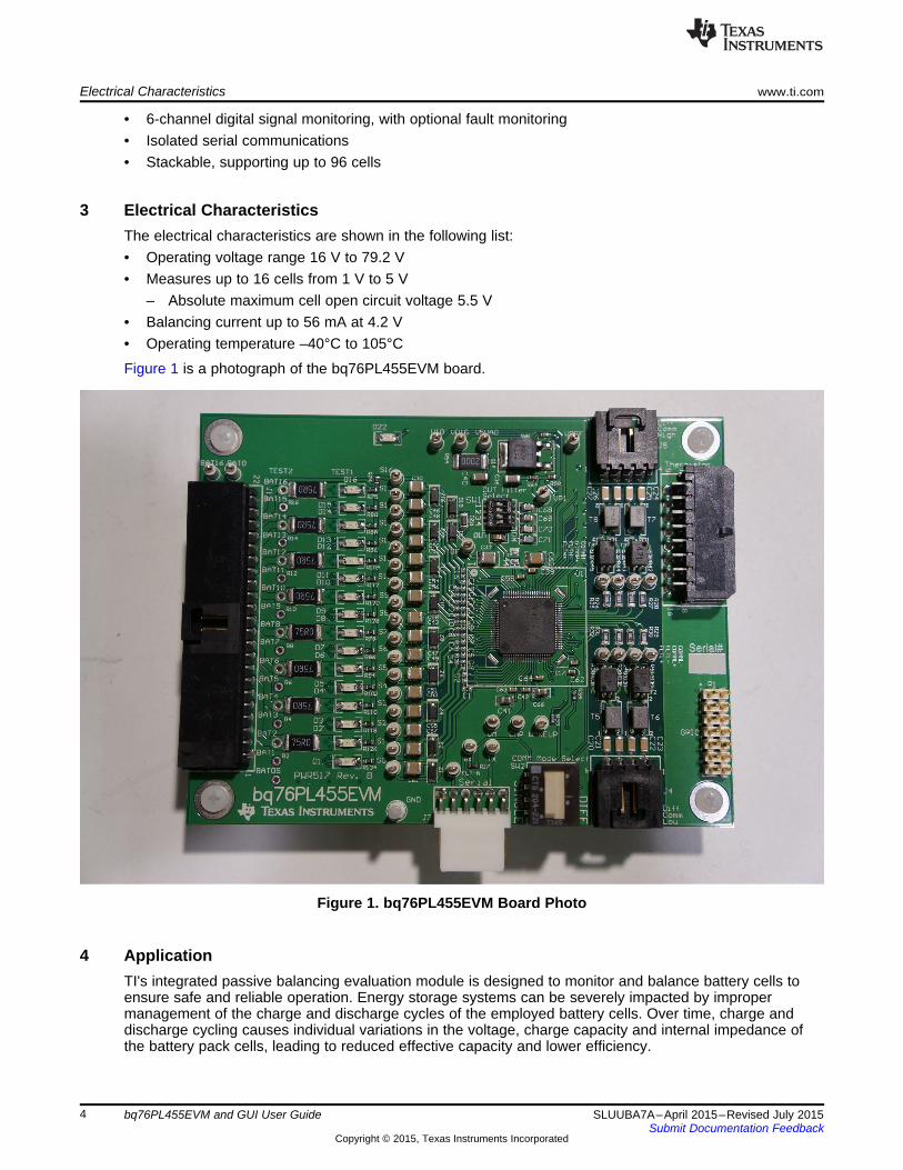
Figure 1 is a photograph of the bq76PL455EVM board.
Figure 1. bq76PL455EVM Board Photo
4 ApplicationTI's integrated passive balancing evaluation module is designed to monitor and balance battery cells toensure safe and reliable operation. Energy storage systems can be severely impacted by impropermanagement of the charge and discharge cycles of the employed battery cells. Over time, charge anddischarge cycling causes individual variations in the voltage, charge capacity and internal impedance ofthe battery pack cells, leading to reduced effective capacity and lower efficiency.
4 bq76PL455EVM and GUI User Guide SLUUBA7A–April 2015–Revised July 2015Submit Documentation Feedback
Copyright © 2015, Texas Instruments Incorporated
www.ti.com Application
If cells are mismatched by charge and discharge cycling, aging, or errors in manufacturing, then the cellscan easily be pushed beyond their rated operating voltage range by further charge and discharge cycles,causing permanent damage and compromising pack performance. Using the bq76PL455A-Q1 monitoringand balancing system, the individual battery pack cells are brought to the same voltage to optimize batterypack charge storage, lifetime, and application run time on a single charge.
The bq76PL455EVM implements the following functions:• Cell voltage monitoring• Cell UV and OV comparators• Cell balancing• Temperature and auxiliary signal monitoring• Embedded control• Fault monitoring• Isolated differential daisy chain communications• PC serial communications• General purpose I/O• Power supply
5SLUUBA7A–April 2015–Revised July 2015 bq76PL455EVM and GUI User GuideSubmit Documentation Feedback
Copyright © 2015, Texas Instruments Incorporated
Registers
Control
Squeeze Resistors
Threshold Set
NPN Regulator
EQ Control
WinComp
VP
NP
NB
TO
P
V5V
AO
VD
IG
VM
CH
M
CH
P
OSC
MUX
OV DAC
UV DAC
10 V ALWAYS ON
4.5V VREF
5.3 V REF
NPN PROTECT
VP CLAMP
1k
2.5V VREF
OU
T2
OU
T1
LPF
RX
ADC MUX ADC
VR
EF
Registers
I/O
TSD
OV
UV
OV
UV
OV
UV
OV
UV
VDIG
VP
VIO
VDD18
V5VAO
ANALOG DIE DIGITAL DIE
VDD18 TX
TX / RX
TX / RX
V5VAO VDIG
ChargePump
VDIG
VP
VM
HIGHESTCELL
EEPROM
VREG1.8
5 V ALWAYS
ON
Comms Interface
AUX0
AUX7
FAULTH-FAULTH+
FAULTL-FAULTL+
COMMH-COMMH+
COMML-COMML+
WAKEUP
RX
TX
POR
VP POR
V5VAO POR
1.8V POR
VIO POR
VDIG POR
POR
VP POR
VDIG POR
VM POR
GP
IO5
GP
IO0
FA
ULT
_NVIO
CG
ND
DG
ND
AG
ND
2
AG
ND
1
TempSensor
AFE
VSENSE0
EQ1
VSENSE1
VSENSE2
EQ2
VSENSE15
EQ16
VSENSE16
Temp Sensor
ChecksumEngine
EEC Decoder
AUX Pullup
AUXPUEN
DigitalComparators
Stack Monitor
AG
ND
3
VTOP
AGND
NPN PROTECT
!
TSD
!
WAKE
WAKEUP
V5VAO
WakeupControl
Registers
Control
WAKEUP
WAKE
Application www.ti.com
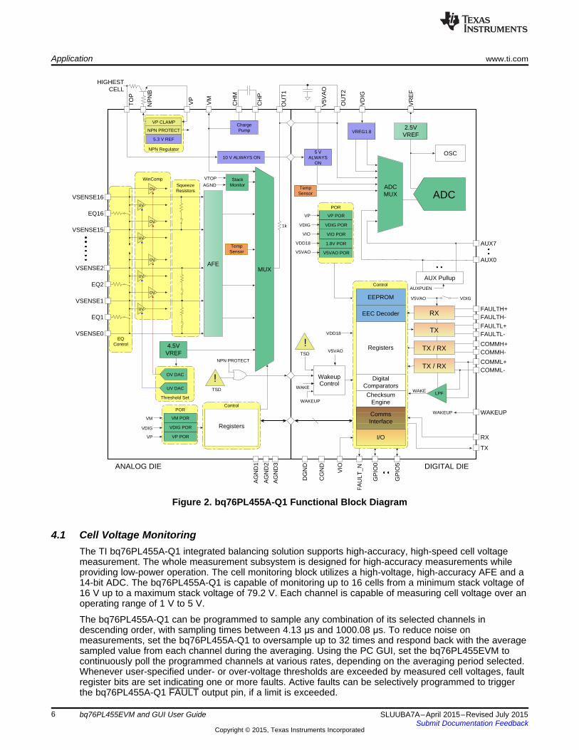
Figure 2. bq76PL455A-Q1 Functional Block Diagram
4.1 Cell Voltage MonitoringThe TI bq76PL455A-Q1 integrated balancing solution supports high-accuracy, high-speed cell voltagemeasurement. The whole measurement subsystem is designed for high-accuracy measurements whileproviding low-power operation. The cell monitoring block utilizes a high-voltage, high-accuracy AFE and a14-bit ADC. The bq76PL455A-Q1 is capable of monitoring up to 16 cells from a minimum stack voltage of16 V up to a maximum stack voltage of 79.2 V. Each channel is capable of measuring cell voltage over anoperating range of 1 V to 5 V.
The bq76PL455A-Q1 can be programmed to sample any combination of its selected channels indescending order, with sampling times between 4.13 μs and 1000.08 μs. To reduce noise onmeasurements, set the bq76PL455A-Q1 to oversample up to 32 times and respond back with the averagesampled value from each channel during the averaging. Using the PC GUI, set the bq76PL455EVM tocontinuously poll the programmed channels at various rates, depending on the averaging period selected.Whenever user-specified under- or over-voltage thresholds are exceeded by measured cell voltages, faultregister bits are set indicating one or more faults. Active faults can be selectively programmed to triggerthe bq76PL455A-Q1 FAULT output pin, if a limit is exceeded.
6 bq76PL455EVM and GUI User Guide SLUUBA7A–April 2015–Revised July 2015Submit Documentation Feedback
Copyright © 2015, Texas Instruments Incorporated
www.ti.com Application
4.2 Cell Undervoltage and Overvoltage ComparatorsAn independent bank of comparators with their own separate undervoltage and overvoltage limits providesadditional cell voltage monitoring and FAULT line control.
4.3 Temperature and Auxiliary Signal MonitoringThe bq76PL455A-Q1 supports eight temperature and auxiliary channels. The bq76PL455EVM implementsa connector for all of these channels, in order to test remote temperature and auxiliary signal monitoring.Negative thermal coefficient (NTC) thermistors or external signals can be connected to thebq76PL455EVM’s 8x2 pin right angle temperature sense J2 - Thermistor connector. Separateundervoltage and overvoltage limits can be set for each of the eight temperature/auxiliary channels. Ifthese limits are reached, a fault is flagged.
10-kΩ pull up resistors are fitted to support NTC use. Choose a thermistor, depending on the applicationand need and change the 10-kΩ pull-up resistors, as required.
4.4 Cell BalancingBased on the cell voltage data, the main system controller can determine when individual cells reach theirmaximum limit during charging. Without passive balancing, if an individual cell reaches its maximumvoltage, then stack charging should stop to prevent overcharging and damaging that cell. However, thatleaves other cells in the same series string less than 100% charged if all of the cells are not evenlymatched and do not reach maximum charge at the same time. Premature termination of stack chargingdue to an individual cell reaching maximum voltage leaves the stack inefficiently charged to less than itstheoretical maximum. With passive balancing, a switchable external shunt resistor across each cell is usedto discharge cells and limit the voltage of individual cells already at maximum voltage to allow furthercharging of the battery pack and raising all the cells to their maximum state of charge. The battery stack ischarged to its true maximum potential with passive balancing.
Each of the 16 battery channels on the evaluation module incorporates an external N-channel MOSFET inseries with a shunt 75-Ω, 1-W resistor across the battery cell. A secondary load is also incorporated in theform of an LED which lights when the MOSFET is on and balancing is active. The 16 N-channelMOSFETs are controlled by 16 EQ lines from the bq76PL455A-Q1 allowing independent balancing ofeach battery as determined from the cell voltage measurements.
To balance an individual cell, the EQ line for the N-Channel MOSFET on the selected channel is drivenhigh. Once it is turned on, current flows through the shunt resistor and LED circuit to dissipate excesscharge. The standard bq76PL455EVM is supplied with 16 × 75-Ω, 1-W (at 25C° ambient) shunt resistorswhich give a 56-mA balancing current for a cell at 4.2 V. Make the shunt resistor values smaller or largerto suit the application requirements. Minimum resistor value and maximum balancing current are limitedonly by the 1 W (at 25C°) power rating of the individual 2512 size balancing resistors and resulting PCBtemperature when all 16 balancing resistors are on.
4.5 Embedded Control LogicThe bq76PL455A-Q1 incorporates control logic to manage serial communications with the PC or mainsystem controller to control the monitoring and balancing functions and to respond back to the PC or mainsystem controller with the requested data.
The bq76PL455A-Q1 embedded control logic uses both EEPROM and RAM to store control register-based configuration data. EEPROM maintains configuration data while the bq76PL455A-Q1 is in powerdown mode. The configuration data is transferred from EEPROM to RAM when the bq76PL455A-Q1wakes; RAM data are used during normal operation. Modify the RAM data with a main system controlleror PC GUI.
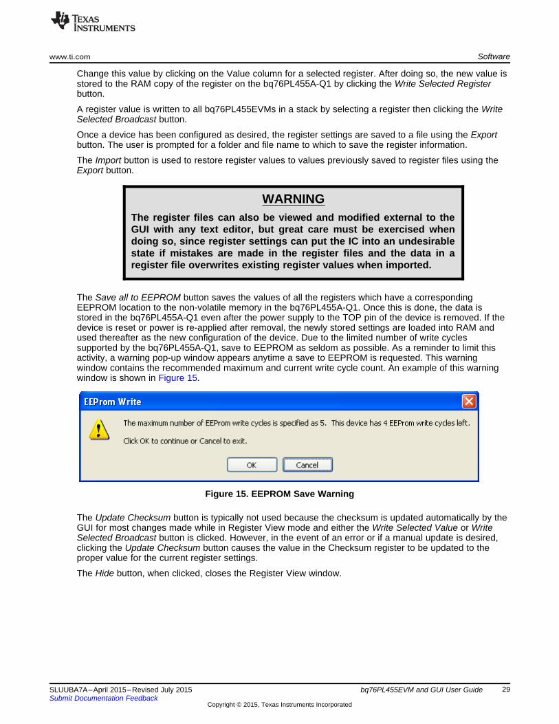
New register settings written into RAM by the system controller or PC GUI can be transferred to EEPROMon the bq76PL455A-Q1 IC if required to be automatically loaded on the next power cycle. In a typical,real-world implementation, the EEPROM is not required to be written frequently, therefore, thebq76PL455A-Q1 EEPROM is designed with limited endurance write cycles unsuited to the evaluationmodule environment.
7SLUUBA7A–April 2015–Revised July 2015 bq76PL455EVM and GUI User GuideSubmit Documentation Feedback
Copyright © 2015, Texas Instruments Incorporated
Application www.ti.com
Consequently, writing RAM register values to EEPROM is enabled but generates a warning message onthe evaluation module. The GUI allows the user to store their own register configurations on the PC as.reg files as an alternative to programming the EEPROM. These configuration files can then be restoredmanually as desired, such as after a power cycle. Alternatively, new configurations for the bq76PL455A-Q1 are written to RAM directly after any new power cycle using the controls in the GUI.
4.6 CommunicationsCommunication between the PC GUI and the first bq76PL455EVM is done via a USB-to-TTL Serialconverter cable. This cable connects to the J3 - Serial connector on the bq76PL455EVM. Communicationbetween all subsequent stacked bq76PL455EVMs is done over isolated, differential twisted pair, daisychained communication lines connected between the J4 - Diff Comm Low and J5 - Diff Comm Highconnectors of neighboring bq76PL455EVMs. The communication rate between the PC and the first ofpotentially multiple stacked modules is adjustable to various baud rates from 125K to 1M, whereas thecommunication rate over the daisy chain link is fixed. The typical minimum bit period over the daisy chainlink is 125 ns (8 MHz). Communication over the differential daisy chain link is transparent to the user viathe GUI, as the conversion between the single-ended communications link and the differentialcommunications link is handled in hardware by the bq76PL455A-Q1.
Communication is mastered by the PC GUI using a command and response protocol which allows theGUI to configure and read back data from slave bq76PL455EVMs. Under the command and responseprotocol, communication with the bq76PL455EVM(s) is always initiated by the GUI which issues acommand frame. Command frames are addressed to either an individual bq76PL455A-Q1, sent as abroadcast to a pre-specified group of consecutively addressed bq76PL455A-Q1 devices, or sent as ageneral broadcast to all bq76PL455A-Q1 devices on the J4 - Diff Comm Low and J5 - Diff Comm Highbus. Some command types are currently supported by the GUI only in the Extended Window interface.
The following six types of command frames are supported by the bq76PL455A-Q1:1. Write to a single bq76PL455A-Q1 causing a returned response (that is, essentially a “read” command).2. Write to a single bq76PL455A-Q1 with no response.3. Write to a pre-defined group of bq76PL455A-Q1 devices to generate a series of responses (device
with highest address in group responds first).4. Write to a pre-defined group of bq76PL455A-Q1 devices without a response request.5. Write to all connected bq76PL455A-Q1 devices to generate a series of responses (device with the
highest address responds first).6. Write to all connected bq76PL455A-Q1 devices with no responses generated.
The GUI currently uses command types 1, 2 and 6 from the aforementioned list during its operation aspart of the graphical interface. The remaining command frame types are accessible only through theextended window manual command interface and scripting options.
On the bq76PL455EVM, high-voltage isolation is provided on all of the twisted pair differentialcommunication links between each stacked evaluation module.
The serial bus allows Command frames to be transmitted by the PC and to be received by allbq76PL455EVMs. Response frames, when requested, are transmitted by any addressed bq76PL455EVMback to the PC.
Since response frames are only ever sent in response to command frames, a single physical pair of wiresis used to communicate between any two neighboring bq76PL455A-Q1 devices in a half duplex manner toalternately send and receive data. The physical differential pair connections are implemented usingcapacitive-coupling and are designed to meet the needs of wired differential communications inautomotive applications.
For battery systems with more than 16 cells where multiple bq76PL455EVMs are stacked, each evaluationmodule must have a unique address. Although the bq76PL455A-Q1 IC allows addresses to be set eitherwith the GPIO lines in hardware or via software, the evaluation module and GUI are, by default, auto-addressed by the GUI when the GUI starts. If more than one evaluation module is connected,bq76PL455EVMs are auto-addressed with addresses from 0 to n – 1, where n is the number of modulesconnected. The bq76PL455EVM connected to the PC is address 0, the first daisy-chained evaluationmodule is at address 1, the second daisy-chained evaluation module is at address 2, and so on.
8 bq76PL455EVM and GUI User Guide SLUUBA7A–April 2015–Revised July 2015Submit Documentation Feedback
Copyright © 2015, Texas Instruments Incorporated
www.ti.com Application
When polling and balancing, the GUI can communicate with multiple bq76PL455EVMs in a stackedconfiguration and log the data received from these evaluation modules to log files stored on the PC, butthe GUI allows data from only a single bq76PL455EVM to be viewed in real time. To switch the real timeview to another bq76PL455EVM, polling and balancing must be stopped, and the user must select a newevaluation module address from the Board Address pull-down menu on the Setup tab, then re-enablepolling or balancing.
4.7 FaultWhen a fault condition is detected, the bq76PL455A-Q1 communicates the fault back to the host PC onthe FAULT pin. Faults from evaluation modules higher in the daisy chain stack are communicated to thebottom (that is, lowest address) evaluation module using the FAULT ±differential signal pairs on the J5 -Diff Comm High and J4 - Diff Comm Low connectors. In the case of the bottom bq76PL455A-Q1, thesingle-ended active low FAULT signal is driven low whenever a fault is detected. Since a single virtualFAULT line is shared by all bq76PL455A-Q1 devices, in a user application the FAULT line going lowshould trigger the system controller to start sending commands to discover which bq76PL455A-Q1detected the fault and understand the nature of that fault so it can take appropriate action.
Currently, the daisy-chained FAULT signal terminates at the lowest evaluation module and the line statusis measured at pin 2 of the J3 - Serial connector. Additionally, a Flt-N test pin is also provided. The GUIautomatically polls the fault registers of thebq76PL455A-Q1 to show current status of all unmasked faults.
4.8 Wake and Power DownThebq76PL455A-Q1 has two power states, On (powered up) and Off (powered down). The power state iscontrolled by a hardware wake signal and a “wake up tone” on the differential twisted pair communicationslink between multiple evaluation modules. In single-ended mode, the bq76PL455A-Q1 uses the WAKEUPsignal (pin 49) as the wake input. When this pin on the bq76PL455A-Q1 is driven high (using an invertedsignal on the J3 - Serial connector), the bottom module in a daisy chain configuration powers on andgenerates a “wake up tone”. This tone is sent to other modules via the differential communication bus.This in turn causes all modules connected to the differential bus to also power on. To power down, thePOWER_DOWN bit in the Device Control Register (address 11) is set by sending a Broadcast Commandto the all bq76PL455A-Q1 devices on the stack while the WAKEUP pin is low on the bottom module.
4.9 Power SuppliesThe bq76PL455EVM is powered from the top of the cell stack being monitored and balanced, which mayrange from 16 V–79.2 V. Although several options exist to post-regulate this high voltage supply down thebq76PL455A-Q1’s integrated linear voltage regulator, the bq76PL455EVM implements a simple drop-down voltage divider. This provides the best low noise performance at the expense of higherbq76PL455EVM current compared to an implementation in which a switching buck converter is used. Aswitching buck converter optimizes efficiency, but compromises noise performance.
The bq76PL455A-Q1 linear voltage controller uses an external NPN power transistor to regulate a 5.3-Voutput supply at VP1. The VP1 supply then drives the VDIG digital supply on the bq76PL455A-Q1. Aseparate external VIO supply line into the bq76PL455A-Q1 is provided by the PC host via pin 3 on the J3- Serial connector. Although it is possible to externally supply the VDIG digital supply, it is notrecommended to do so on the bq76PL455EVM.
The bq76PL455A-Q1 also produces a regulated 1.8-V supply for internal use and a 2.5-V reference foruse by the integrated 14-bit ADC. There is no external (pin) access to the 1.8-V supply.
9SLUUBA7A–April 2015–Revised July 2015 bq76PL455EVM and GUI User GuideSubmit Documentation Feedback
Copyright © 2015, Texas Instruments Incorporated
Hardware www.ti.com
5 Hardware
5.1 SwitchesThere are 2 DIP switch packages on the bq76PL455EVM. The DIP packages provide five individual switchlevers. Configure the switch levers prior to application of bq76PL455EVM power. The switch packagedesignations are:• SW1 - OUT Filter Select switch package• SW2 - COMM Mode Select switch package
WARNINGChanging switch positions with power connected to the evaluationmodule can cause damage to the bq76PL455EVM.
The operation of the switch packages are detailed in Section 5.1.1 through Section 5.1.2.
5.1.1 SW1 - OUT Filter SelectThis 4-position DIP switch is used to connect different capacitor values to OUT1/OUT2, the output of theAFE before it enters the 14-bit ADC for conversion. This allows different single-pole low pass filters to beused in the signal path depending on the ADC sampling configuration selected in the GUI.
NOTE: NOTE: The current version of the GUI reads and displays the sample periods from theappropriate registers in the bq76PL455A-Q1 devices with which it is communicating. Bydefault at the time of writing, bq76PL455A-Q1 devices are configured to sample the cellchannels at 60.04 µs with 8x averaging (staying on a single channel before moving on to thenext channel). For this configuration, the best external capacitor selection is 390 pF. Pleasebe sure to change the corresponding SW1 - OUT Filter Select switch if the GUI samplingperiod configuration is changed.
Switch positions on the SW1 - OUT Filter Select switch package are marked with the numbers ‘1’ through‘4’ on one side of the package, and marked with the word “ON” on the other side of the switch package.
To select the 390 pF recommended for the default configuration, set only switch 4 to the “ON” position.
If changing the default sampling configuration, for example to a single sample (that is, no averaging)setting at 99.92 µs, other capacitors must be switched into the circuit.
10 bq76PL455EVM and GUI User Guide SLUUBA7A–April 2015–Revised July 2015Submit Documentation Feedback
Copyright © 2015, Texas Instruments Incorporated
www.ti.com Hardware
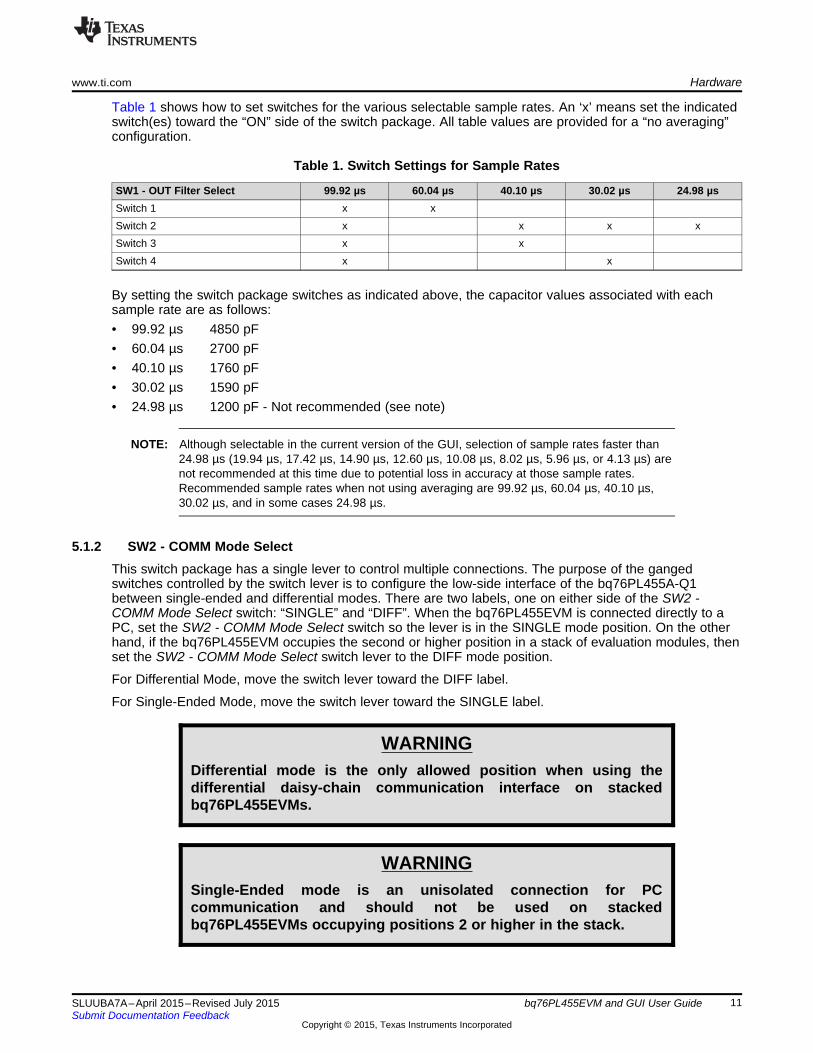
Table 1 shows how to set switches for the various selectable sample rates. An ‘x’ means set the indicatedswitch(es) toward the “ON” side of the switch package. All table values are provided for a “no averaging”configuration.
Table 1. Switch Settings for Sample Rates
SW1 - OUT Filter Select 99.92 µs 60.04 µs 40.10 µs 30.02 µs 24.98 µsSwitch 1 x xSwitch 2 x x x xSwitch 3 x xSwitch 4 x x
By setting the switch package switches as indicated above, the capacitor values associated with eachsample rate are as follows:• 99.92 µsxxxx4850 pF• 60.04 µsxxxx2700 pF• 40.10 µsxxxx1760 pF• 30.02 µsxxxx1590 pF• 24.98 µsxxxx1200 pF - Not recommended (see note)
NOTE: Although selectable in the current version of the GUI, selection of sample rates faster than24.98 µs (19.94 µs, 17.42 µs, 14.90 µs, 12.60 µs, 10.08 µs, 8.02 µs, 5.96 µs, or 4.13 µs) arenot recommended at this time due to potential loss in accuracy at those sample rates.Recommended sample rates when not using averaging are 99.92 µs, 60.04 µs, 40.10 µs,30.02 µs, and in some cases 24.98 µs.
5.1.2 SW2 - COMM Mode SelectThis switch package has a single lever to control multiple connections. The purpose of the gangedswitches controlled by the switch lever is to configure the low-side interface of the bq76PL455A-Q1between single-ended and differential modes. There are two labels, one on either side of the SW2 -COMM Mode Select switch: “SINGLE” and “DIFF”. When the bq76PL455EVM is connected directly to aPC, set the SW2 - COMM Mode Select switch so the lever is in the SINGLE mode position. On the otherhand, if the bq76PL455EVM occupies the second or higher position in a stack of evaluation modules, thenset the SW2 - COMM Mode Select switch lever to the DIFF mode position.
For Differential Mode, move the switch lever toward the DIFF label.
For Single-Ended Mode, move the switch lever toward the SINGLE label.
WARNINGDifferential mode is the only allowed position when using thedifferential daisy-chain communication interface on stackedbq76PL455EVMs.
WARNINGSingle-Ended mode is an unisolated connection for PCcommunication and should not be used on stackedbq76PL455EVMs occupying positions 2 or higher in the stack.
11SLUUBA7A–April 2015–Revised July 2015 bq76PL455EVM and GUI User GuideSubmit Documentation Feedback
Copyright © 2015, Texas Instruments Incorporated
Hardware www.ti.com
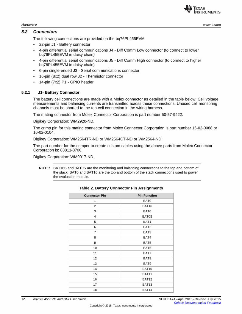
5.2 ConnectorsThe following connections are provided on the bq76PL455EVM:• 22-pin J1 - Battery connector• 4-pin differential serial communications J4 - Diff Comm Low connector (to connect to lower
bq76PL455EVM in daisy chain)• 4-pin differential serial communications J5 - Diff Comm High connector (to connect to higher
bq76PL455EVM in daisy chain)• 6-pin single-ended J3 - Serial communications connector• 16-pin (8x2) dual row J2 - Thermistor connector• 14-pin (7x2) P1 - GPIO header
5.2.1 J1- Battery ConnectorThe battery cell connections are made with a Molex connector as detailed in the table below. Cell voltagemeasurements and balancing currents are transmitted across these connections. Unused cell monitoringchannels must be shorted to the top cell connection in the wiring harness.
The mating connector from Molex Connector Corporation is part number 50-57-9422.
Digikey Corporation: WM2920-ND.
The crimp pin for this mating connector from Molex Connector Corporation is part number 16-02-0088 or16-02-0104.
Digikey Corporation: WM2564TR-ND or WM2564CT-ND or WM2564-ND.
The part number for the crimper to create custom cables using the above parts from Molex ConnectorCorporation is: 63811-8700.
Digikey Corporation: WM9017-ND.
NOTE: BAT16S and BAT0S are the monitoring and balancing connections to the top and bottom ofthe stack. BAT0 and BAT16 are the top and bottom of the stack connections used to powerthe evaluation module.
Table 2. Battery Connector Pin Assignments
Connector Pin Pin Function1 BAT02 BAT163 BAT04 BAT0S5 BAT16 BAT27 BAT38 BAT49 BAT510 BAT611 BAT712 BAT813 BAT914 BAT1015 BAT1116 BAT1217 BAT1318 BAT14
12 bq76PL455EVM and GUI User Guide SLUUBA7A–April 2015–Revised July 2015Submit Documentation Feedback
Copyright © 2015, Texas Instruments Incorporated
www.ti.com Hardware
Table 2. Battery Connector PinAssignments (continued)
Connector Pin Pin Function19 BAT1520 BAT16S21 BAT1622 BAT0
NOTE: All signals with like names are connected together on the bq76PL455A-Q1 PCB. Pins 1 and22 of the J1 – Battery connector are identified with silkscreen markings.
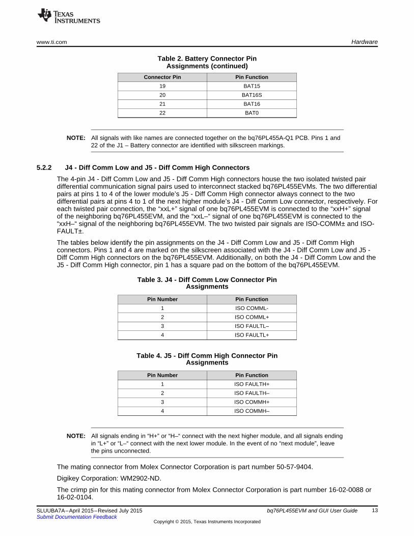
5.2.2 J4 - Diff Comm Low and J5 - Diff Comm High ConnectorsThe 4-pin J4 - Diff Comm Low and J5 - Diff Comm High connectors house the two isolated twisted pairdifferential communication signal pairs used to interconnect stacked bq76PL455EVMs. The two differentialpairs at pins 1 to 4 of the lower module’s J5 - Diff Comm High connector always connect to the twodifferential pairs at pins 4 to 1 of the next higher module’s J4 - Diff Comm Low connector, respectively. Foreach twisted pair connection, the “xxL+” signal of one bq76PL455EVM is connected to the “xxH+” signalof the neighboring bq76PL455EVM, and the “xxL–“ signal of one bq76PL455EVM is connected to the“xxH–“ signal of the neighboring bq76PL455EVM. The two twisted pair signals are ISO-COMM± and ISO-FAULT±.
The tables below identify the pin assignments on the J4 - Diff Comm Low and J5 - Diff Comm Highconnectors. Pins 1 and 4 are marked on the silkscreen associated with the J4 - Diff Comm Low and J5 -Diff Comm High connectors on the bq76PL455EVM. Additionally, on both the J4 - Diff Comm Low and theJ5 - Diff Comm High connector, pin 1 has a square pad on the bottom of the bq76PL455EVM.
Table 3. J4 - Diff Comm Low Connector PinAssignments
Pin Number Pin Function1 ISO COMML-2 ISO COMML+3 ISO FAULTL–4 ISO FAULTL+
Table 4. J5 - Diff Comm High Connector PinAssignments
Pin Number Pin Function1 ISO FAULTH+2 ISO FAULTH–3 ISO COMMH+4 ISO COMMH–
NOTE: All signals ending in “H+” or “H–“ connect with the next higher module, and all signals endingin “L+” or “L–“ connect with the next lower module. In the event of no “next module”, leavethe pins unconnected.
The mating connector from Molex Connector Corporation is part number 50-57-9404.
Digikey Corporation: WM2902-ND.
The crimp pin for this mating connector from Molex Connector Corporation is part number 16-02-0088 or16-02-0104.
13SLUUBA7A–April 2015–Revised July 2015 bq76PL455EVM and GUI User GuideSubmit Documentation Feedback
Copyright © 2015, Texas Instruments Incorporated
Hardware www.ti.com
Digikey Corporation: WM2564TR-ND or WM2564CT-ND or WM2564-ND.
The part number for the crimper to create custom cables using the above parts from Molex ConnectorCorporation is: 63811-8700.
Digikey Corporation: WM9017-ND.
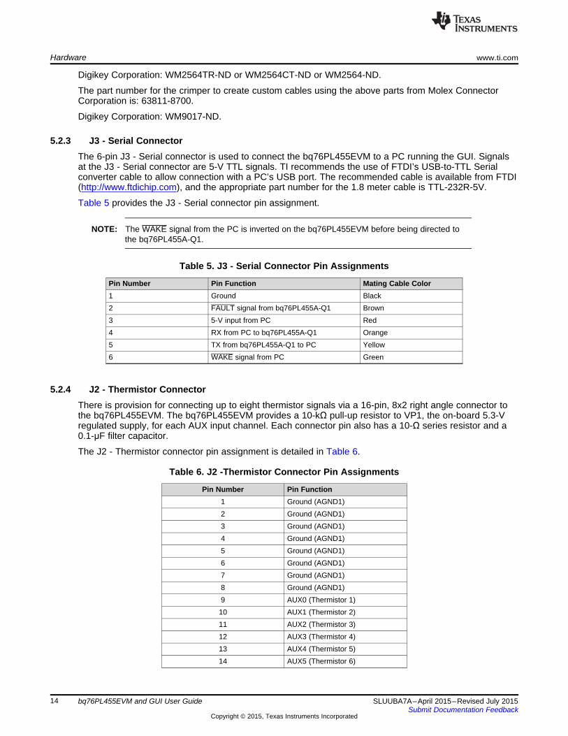
5.2.3 J3 - Serial ConnectorThe 6-pin J3 - Serial connector is used to connect the bq76PL455EVM to a PC running the GUI. Signalsat the J3 - Serial connector are 5-V TTL signals. TI recommends the use of FTDI’s USB-to-TTL Serialconverter cable to allow connection with a PC’s USB port. The recommended cable is available from FTDI(http://www.ftdichip.com), and the appropriate part number for the 1.8 meter cable is TTL-232R-5V.
Table 5 provides the J3 - Serial connector pin assignment.
NOTE: The WAKE signal from the PC is inverted on the bq76PL455EVM before being directed tothe bq76PL455A-Q1.
Table 5. J3 - Serial Connector Pin Assignments
Pin Number Pin Function Mating Cable Color1 Ground Black2 FAULT signal from bq76PL455A-Q1 Brown3 5-V input from PC Red4 RX from PC to bq76PL455A-Q1 Orange5 TX from bq76PL455A-Q1 to PC Yellow6 WAKE signal from PC Green
5.2.4 J2 - Thermistor ConnectorThere is provision for connecting up to eight thermistor signals via a 16-pin, 8x2 right angle connector tothe bq76PL455EVM. The bq76PL455EVM provides a 10-kΩ pull-up resistor to VP1, the on-board 5.3-Vregulated supply, for each AUX input channel. Each connector pin also has a 10-Ω series resistor and a0.1-μF filter capacitor.
The J2 - Thermistor connector pin assignment is detailed in Table 6.
Table 6. J2 -Thermistor Connector Pin Assignments
Pin Number Pin Function1 Ground (AGND1)2 Ground (AGND1)3 Ground (AGND1)4 Ground (AGND1)5 Ground (AGND1)6 Ground (AGND1)7 Ground (AGND1)8 Ground (AGND1)9 AUX0 (Thermistor 1)10 AUX1 (Thermistor 2)11 AUX2 (Thermistor 3)12 AUX3 (Thermistor 4)13 AUX4 (Thermistor 5)14 AUX5 (Thermistor 6)
14 bq76PL455EVM and GUI User Guide SLUUBA7A–April 2015–Revised July 2015Submit Documentation Feedback
Copyright © 2015, Texas Instruments Incorporated
www.ti.com Hardware
Table 6. J2 -Thermistor Connector PinAssignments (continued)
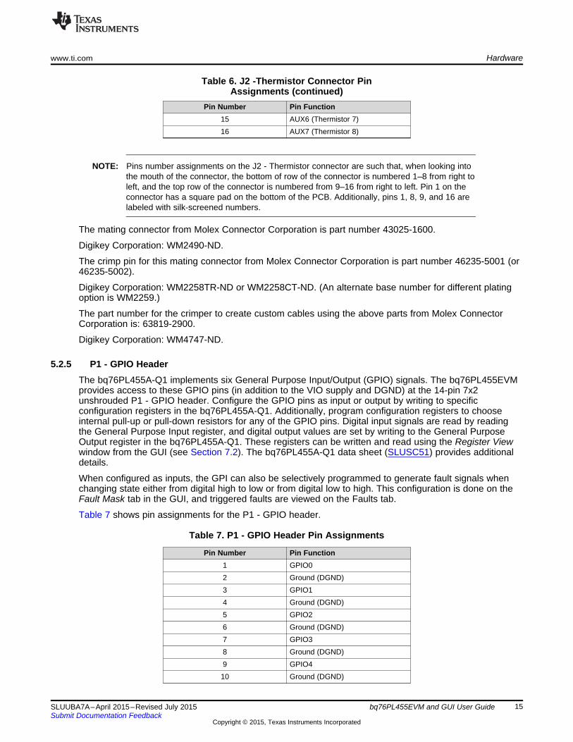
Pin Number Pin Function15 AUX6 (Thermistor 7)16 AUX7 (Thermistor 8)
NOTE: Pins number assignments on the J2 - Thermistor connector are such that, when looking intothe mouth of the connector, the bottom of row of the connector is numbered 1–8 from right toleft, and the top row of the connector is numbered from 9–16 from right to left. Pin 1 on theconnector has a square pad on the bottom of the PCB. Additionally, pins 1, 8, 9, and 16 arelabeled with silk-screened numbers.
The mating connector from Molex Connector Corporation is part number 43025-1600.
Digikey Corporation: WM2490-ND.
The crimp pin for this mating connector from Molex Connector Corporation is part number 46235-5001 (or46235-5002).
Digikey Corporation: WM2258TR-ND or WM2258CT-ND. (An alternate base number for different platingoption is WM2259.)
The part number for the crimper to create custom cables using the above parts from Molex ConnectorCorporation is: 63819-2900.
Digikey Corporation: WM4747-ND.
5.2.5 P1 - GPIO HeaderThe bq76PL455A-Q1 implements six General Purpose Input/Output (GPIO) signals. The bq76PL455EVMprovides access to these GPIO pins (in addition to the VIO supply and DGND) at the 14-pin 7x2unshrouded P1 - GPIO header. Configure the GPIO pins as input or output by writing to specificconfiguration registers in the bq76PL455A-Q1. Additionally, program configuration registers to chooseinternal pull-up or pull-down resistors for any of the GPIO pins. Digital input signals are read by readingthe General Purpose Input register, and digital output values are set by writing to the General PurposeOutput register in the bq76PL455A-Q1. These registers can be written and read using the Register Viewwindow from the GUI (see Section 7.2). The bq76PL455A-Q1 data sheet (SLUSC51) provides additionaldetails.
When configured as inputs, the GPI can also be selectively programmed to generate fault signals whenchanging state either from digital high to low or from digital low to high. This configuration is done on theFault Mask tab in the GUI, and triggered faults are viewed on the Faults tab.
Table 7 shows pin assignments for the P1 - GPIO header.
Table 7. P1 - GPIO Header Pin Assignments
Pin Number Pin Function1 GPIO02 Ground (DGND)3 GPIO14 Ground (DGND)5 GPIO26 Ground (DGND)7 GPIO38 Ground (DGND)9 GPIO410 Ground (DGND)
15SLUUBA7A–April 2015–Revised July 2015 bq76PL455EVM and GUI User GuideSubmit Documentation Feedback
Copyright © 2015, Texas Instruments Incorporated
Hardware www.ti.com
Table 7. P1 - GPIO Header PinAssignments (continued)
Pin Number Pin Function11 GPIO512 Ground (DGND)13 VIO14 Ground (DGND)
NOTE: The P1 - GPIO header is a 7x2 dual row unshrouded header. Pin 1 has a square pad on theunderside of the PCB, and the silk screen for the header indicates pin 1 with a small whitedot. All even numbered pins are on one, and all odd numbered pins are on the other, row ofthe header.
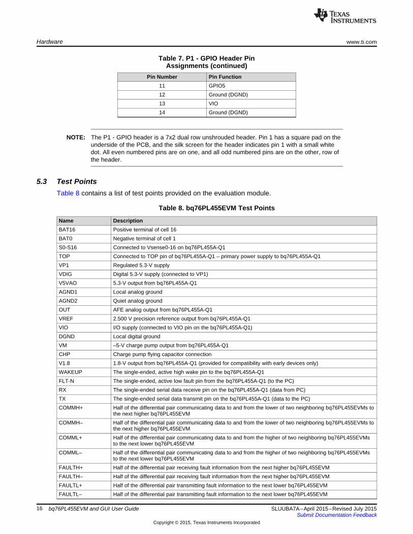
5.3 Test PointsTable 8 contains a list of test points provided on the evaluation module.
Table 8. bq76PL455EVM Test Points
Name DescriptionBAT16 Positive terminal of cell 16BAT0 Negative terminal of cell 1S0-S16 Connected to Vsense0-16 on bq76PL455A-Q1TOP Connected to TOP pin of bq76PL455A-Q1 – primary power supply to bq76PL455A-Q1VP1 Regulated 5.3-V supplyVDIG Digital 5.3-V supply (connected to VP1)V5VAO 5.3-V output from bq76PL455A-Q1AGND1 Local analog groundAGND2 Quiet analog groundOUT AFE analog output from bq76PL455A-Q1VREF 2.500 V precision reference output from bq76PL455A-Q1VIO I/O supply (connected to VIO pin on the bq76PL455A-Q1)DGND Local digital groundVM –5-V charge pump output from bq76PL455A-Q1CHP Charge pump flying capacitor connectionV1.8 1.8-V output from bq76PL455A-Q1 (provided for compatibility with early devices only)WAKEUP The single-ended, active high wake pin to the bq76PL455A-Q1FLT-N The single-ended, active low fault pin from the bq76PL455A-Q1 (to the PC)RX The single-ended serial data receive pin on the bq76PL455A-Q1 (data from PC)TX The single-ended serial data transmit pin on the bq76PL455A-Q1 (data to the PC)COMMH+ Half of the differential pair communicating data to and from the lower of two neighboring bq76PL455EVMs to
the next higher bq76PL455EVMCOMMH– Half of the differential pair communicating data to and from the lower of two neighboring bq76PL455EVMs to
the next higher bq76PL455EVMCOMML+ Half of the differential pair communicating data to and from the higher of two neighboring bq76PL455EVMs
to the next lower bq76PL455EVMCOMML– Half of the differential pair communicating data to and from the higher of two neighboring bq76PL455EVMs
to the next lower bq76PL455EVMFAULTH+ Half of the differential pair receiving fault information from the next higher bq76PL455EVMFAULTH– Half of the differential pair receiving fault information from the next higher bq76PL455EVMFAULTL+ Half of the differential pair transmitting fault information to the next lower bq76PL455EVMFAULTL– Half of the differential pair transmitting fault information to the next lower bq76PL455EVM
16 bq76PL455EVM and GUI User Guide SLUUBA7A–April 2015–Revised July 2015Submit Documentation Feedback
Copyright © 2015, Texas Instruments Incorporated
www.ti.com Getting Started with the bq76PL455EVM
6 Getting Started with the bq76PL455EVMThe following sequence is recommended to use the bq76PL455A-Q1 evaluation module:1. Install the GUI on the PC.2. Configure the bq76PL455EVM DIP switches.3. Connect the bq76PL455EVM to the battery stack and PC.4. Start the GUI and configure the bq76PL455A-Q1 control registers.5. Start polling, balancing and monitoring status.6. Stop polling, stop balancing.7. Exit the GUI.
These steps are detailed in subsequent sections of this document.
6.1 Software DriversAn FTDI FT232R USB-to-UART adapter driver is required to connect to the passive balancing evaluationmodule to a PC. The driver is either installed automatically as part of the cable install when installing theTTL-232R-5V from FTDI, or download it from www.ftdichip.com/Drivers/VCP.htm.
6.2 GUIIncluded with the TI passive balancing evaluation module is a PC GUI. The GUI is used to configure theevaluation module, read out and log all cell voltage data, control balancing, and manage faults.
The primary parameters configurable in the GUI are as follows:• Number of batteries/series cells in each module• Overvoltage and undervoltage threshold limits• Balancing period• Fault conditions• Communication and parameters
6.3 Recommended PC RequirementsThe requirements for the PC are listed below:• Microsoft® Windows® XP system and above• Intel® CoreTM2 Duo processor with vProTM technology at 2 GHz• 1 GB RAM Core 2 Duo™• 1024 x 768 display VPro™• 4MB hard drive space• USB 2.0 port
17SLUUBA7A–April 2015–Revised July 2015 bq76PL455EVM and GUI User GuideSubmit Documentation Feedback
Copyright © 2015, Texas Instruments Incorporated
Getting Started with the bq76PL455EVM www.ti.com
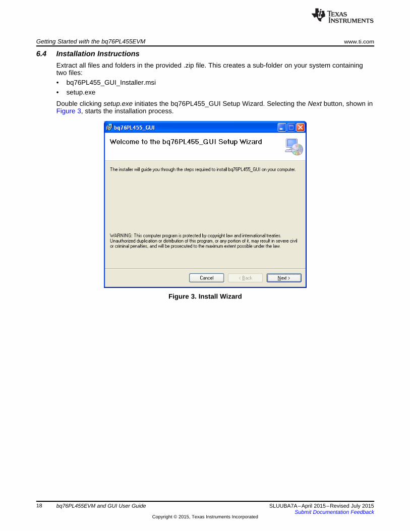
6.4 Installation InstructionsExtract all files and folders in the provided .zip file. This creates a sub-folder on your system containingtwo files:• bq76PL455_GUI_Installer.msi• setup.exe
Double clicking setup.exe initiates the bq76PL455_GUI Setup Wizard. Selecting the Next button, shown inFigure 3, starts the installation process.
Figure 3. Install Wizard
18 bq76PL455EVM and GUI User Guide SLUUBA7A–April 2015–Revised July 2015Submit Documentation Feedback
Copyright © 2015, Texas Instruments Incorporated
www.ti.com Getting Started with the bq76PL455EVM
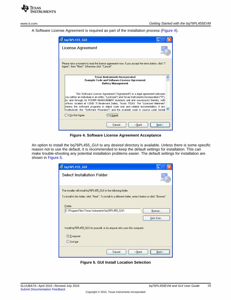
A Software License Agreement is required as part of the installation process (Figure 4).
Figure 4. Software License Agreement Acceptance
An option to install the bq76PL455_GUI to any desired directory is available. Unless there is some specificreason not to use the default, it is recommended to keep the default settings for installation. This canmake trouble-shooting any potential installation problems easier. The default settings for installation areshown in Figure 5.
Figure 5. GUI Install Location Selection
19SLUUBA7A–April 2015–Revised July 2015 bq76PL455EVM and GUI User GuideSubmit Documentation Feedback
Copyright © 2015, Texas Instruments Incorporated
Getting Started with the bq76PL455EVM www.ti.com
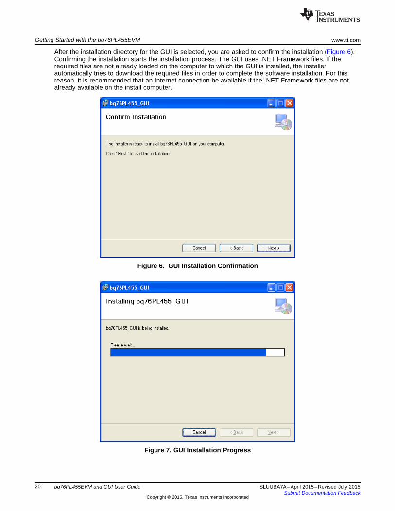
After the installation directory for the GUI is selected, you are asked to confirm the installation (Figure 6).Confirming the installation starts the installation process. The GUI uses .NET Framework files. If therequired files are not already loaded on the computer to which the GUI is installed, the installerautomatically tries to download the required files in order to complete the software installation. For thisreason, it is recommended that an Internet connection be available if the .NET Framework files are notalready available on the install computer.
Figure 6. GUI Installation Confirmation
Figure 7. GUI Installation Progress
20 bq76PL455EVM and GUI User Guide SLUUBA7A–April 2015–Revised July 2015Submit Documentation Feedback
Copyright © 2015, Texas Instruments Incorporated
www.ti.com Getting Started with the bq76PL455EVM
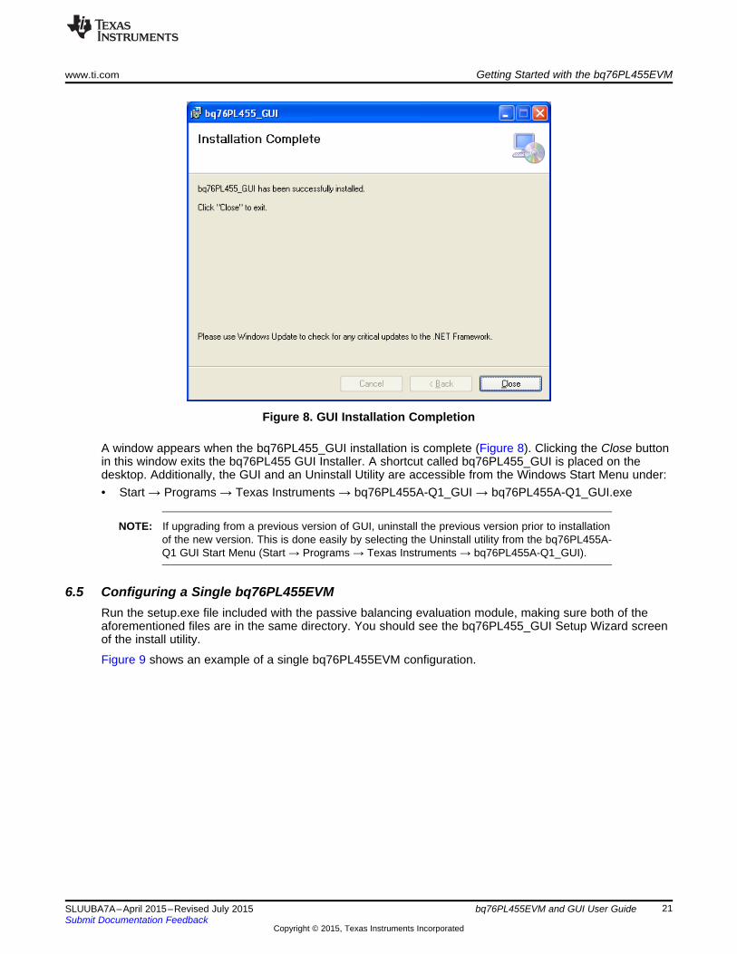
Figure 8. GUI Installation Completion
A window appears when the bq76PL455_GUI installation is complete (Figure 8). Clicking the Close buttonin this window exits the bq76PL455 GUI Installer. A shortcut called bq76PL455_GUI is placed on thedesktop. Additionally, the GUI and an Uninstall Utility are accessible from the Windows Start Menu under:• Start → Programs → Texas Instruments → bq76PL455A-Q1_GUI → bq76PL455A-Q1_GUI.exe
NOTE: If upgrading from a previous version of GUI, uninstall the previous version prior to installationof the new version. This is done easily by selecting the Uninstall utility from the bq76PL455A-Q1 GUI Start Menu (Start → Programs → Texas Instruments → bq76PL455A-Q1_GUI).
6.5 Configuring a Single bq76PL455EVMRun the setup.exe file included with the passive balancing evaluation module, making sure both of theaforementioned files are in the same directory. You should see the bq76PL455_GUI Setup Wizard screenof the install utility.
Figure 9 shows an example of a single bq76PL455EVM configuration.
21SLUUBA7A–April 2015–Revised July 2015 bq76PL455EVM and GUI User GuideSubmit Documentation Feedback
Copyright © 2015, Texas Instruments Incorporated
Getting Started with the bq76PL455EVM www.ti.com
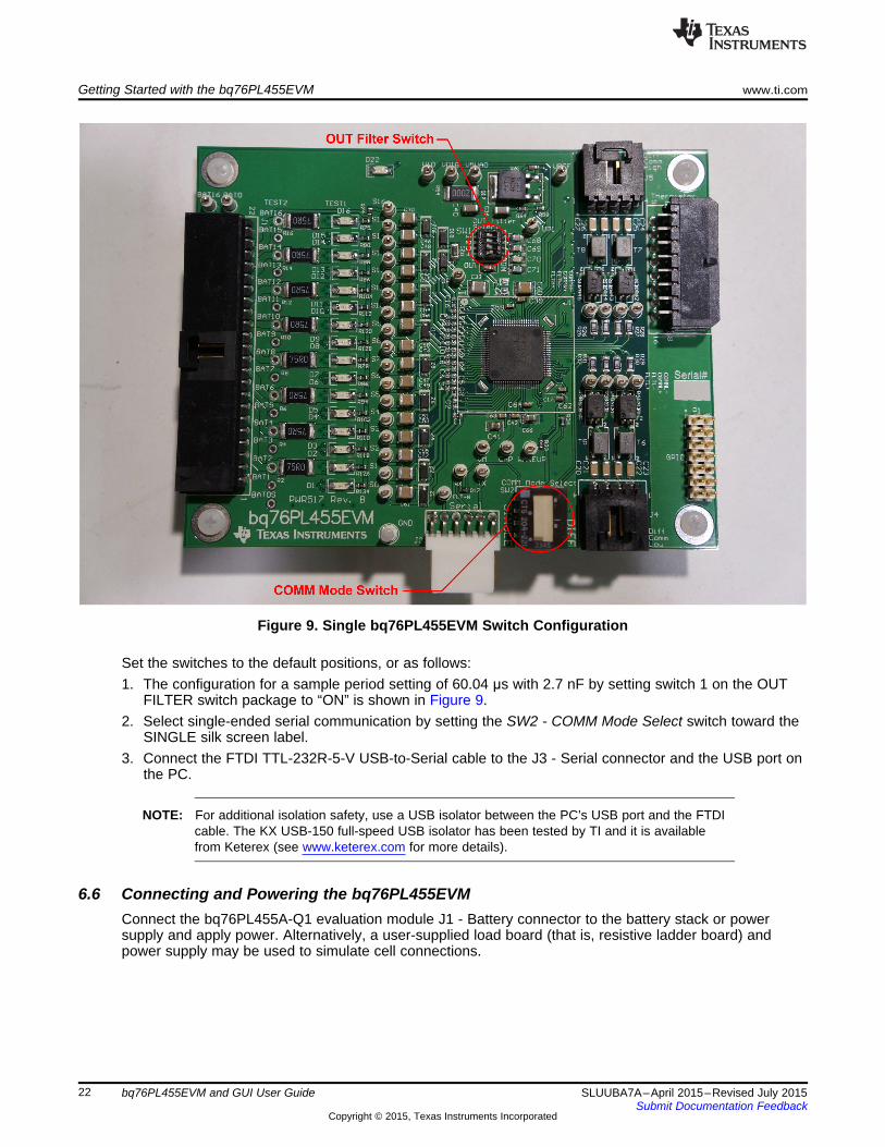
Figure 9. Single bq76PL455EVM Switch Configuration
Set the switches to the default positions, or as follows:1. The configuration for a sample period setting of 60.04 μs with 2.7 nF by setting switch 1 on the OUT
FILTER switch package to “ON” is shown in Figure 9.2. Select single-ended serial communication by setting the SW2 - COMM Mode Select switch toward the
SINGLE silk screen label.3. Connect the FTDI TTL-232R-5-V USB-to-Serial cable to the J3 - Serial connector and the USB port on
the PC.
NOTE: For additional isolation safety, use a USB isolator between the PC’s USB port and the FTDIcable. The KX USB-150 full-speed USB isolator has been tested by TI and it is availablefrom Keterex (see www.keterex.com for more details).
6.6 Connecting and Powering the bq76PL455EVMConnect the bq76PL455A-Q1 evaluation module J1 - Battery connector to the battery stack or powersupply and apply power. Alternatively, a user-supplied load board (that is, resistive ladder board) andpower supply may be used to simulate cell connections.
22 bq76PL455EVM and GUI User Guide SLUUBA7A–April 2015–Revised July 2015Submit Documentation Feedback
Copyright © 2015, Texas Instruments Incorporated
www.ti.com Getting Started with the bq76PL455EVM
NOTE: Although it is not strictly required due to the presence of on-module protection circuitry, whenusing a battery stack, it is recommended to first apply power from the top and bottom of thestack to BAT16 and BAT0, respectively, in order to power the bq76PL455EVM, beforeapplying power from the intermediate stack cell connections to BAT0S, BAT1, BAT2 throughto BAT15, and BAT16S. This is achieved using a make-first, break-last type batteryconnector if hot plugging or using switches to sequence power application.
Start the GUI. This step is explained in greater detail in the Section 7 of this document.
6.7 Configuring Stacked bq76PL455EVMsInstructions for configuring stacked bq76PL455EVMs are as follows:1. Identify the bq76PL455EVM that is connected to the bottom 16-cell module and the bq76PL455EVMs
that is stacked above it - connected to the higher 16-cell modules within the battery system. On thebottom bq76PL455EVM that is connected to the PC, connect the bottom end of the twisted pair daisychain cable to the J5 - Diff Comm High connector. Then, connect the other end of this twisted pairdaisy chain cable to the J4 - Diff Comm Low connecter on the second bq76PL455EVM. Continue withthis pattern for all subsequent bq76PL455EVMs in the daisy chain stack.
2. On the bottom bq76PL455EVM that is connected to the PC, set the SW2 - COMM Mode Select switchas shown in Figure 9. On all other stacked bq76PL455EVMs, set the lever on the SW2 - COMM ModeSelect switch package in the opposite direction, toward the DIFF label
3. Set SW1 - OUT Filter Select switches on all bq76PL455EVMs to the desired setting as outlined inSection 5.1.1 or as shown in Figure 9.
4. Connect any desired temperature sensors to the J2 - Thermistor connector on any of thebq76PL455EVMs in the system.
5. Connect the lowest bq76PL455EVM J3 - Serial header to a PC USB port using an FTDI USB-to-TTLSerial (5 V) cable.
6.8 Connecting and Powering Stacked bq76PL455EVMsPower a stack of bq76PL455EVMs, as configured in the previous section, with the following steps:1. Connect the bottom evaluation module J1 - Battery connector to the lowest 16 cells of the battery stack
and apply power.
NOTE: When using a battery stack, it is recommended - although not strictly required - to first applypower from the top and bottom of the stack to BAT16 and BAT0 respectively in order topower the bq76PL455EVM, before applying power from the intermediate stack cellconnections to BAT0S, BAT1, BAT2 through to BAT15 and BAT16S. This is achieved usinga make-first, break-last type battery connector if hot plugging or using switches to sequencepower application.
2. Connect the next higher stacked evaluation module to the next higher set of 16 cells, for example, cells17–32, using the same relative powering sequence described in step 1. Then, connectbq76PL455EVM 3 to cells 33–48, and so on.
3. Start the GUI (as described in Section 7.1).
7 Software
7.1 Using the SoftwareStart the GUI by double-clicking the bq76PL455_GUI shortcut on the PC desktop. A prompt is presentedto select the COM port number for the Serial-to-USB connection, as shown in Figure 10 and Figure 11. Inmost cases, the highlighted COM port is the appropriate COM port. If this is not the case, due to a custominstallation, determine the appropriate COM port by checking the Ports section in the Windows DeviceManager.
23SLUUBA7A–April 2015–Revised July 2015 bq76PL455EVM and GUI User GuideSubmit Documentation Feedback
Copyright © 2015, Texas Instruments Incorporated
Software www.ti.com
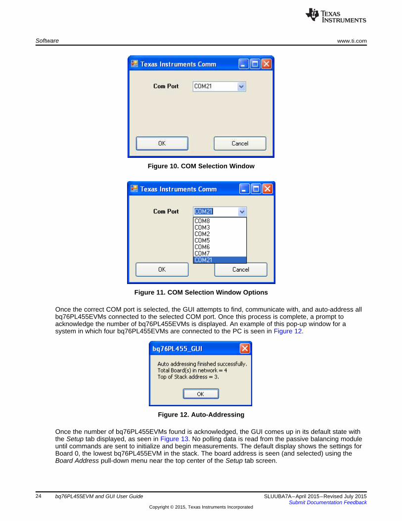
Figure 10. COM Selection Window
Figure 11. COM Selection Window Options
Once the correct COM port is selected, the GUI attempts to find, communicate with, and auto-address allbq76PL455EVMs connected to the selected COM port. Once this process is complete, a prompt toacknowledge the number of bq76PL455EVMs is displayed. An example of this pop-up window for asystem in which four bq76PL455EVMs are connected to the PC is seen in Figure 12.
Figure 12. Auto-Addressing
Once the number of bq76PL455EVMs found is acknowledged, the GUI comes up in its default state withthe Setup tab displayed, as seen in Figure 13. No polling data is read from the passive balancing moduleuntil commands are sent to initialize and begin measurements. The default display shows the settings forBoard 0, the lowest bq76PL455EVM in the stack. The board address is seen (and selected) using theBoard Address pull-down menu near the top center of the Setup tab screen.
24 bq76PL455EVM and GUI User Guide SLUUBA7A–April 2015–Revised July 2015Submit Documentation Feedback
Copyright © 2015, Texas Instruments Incorporated
www.ti.com Software
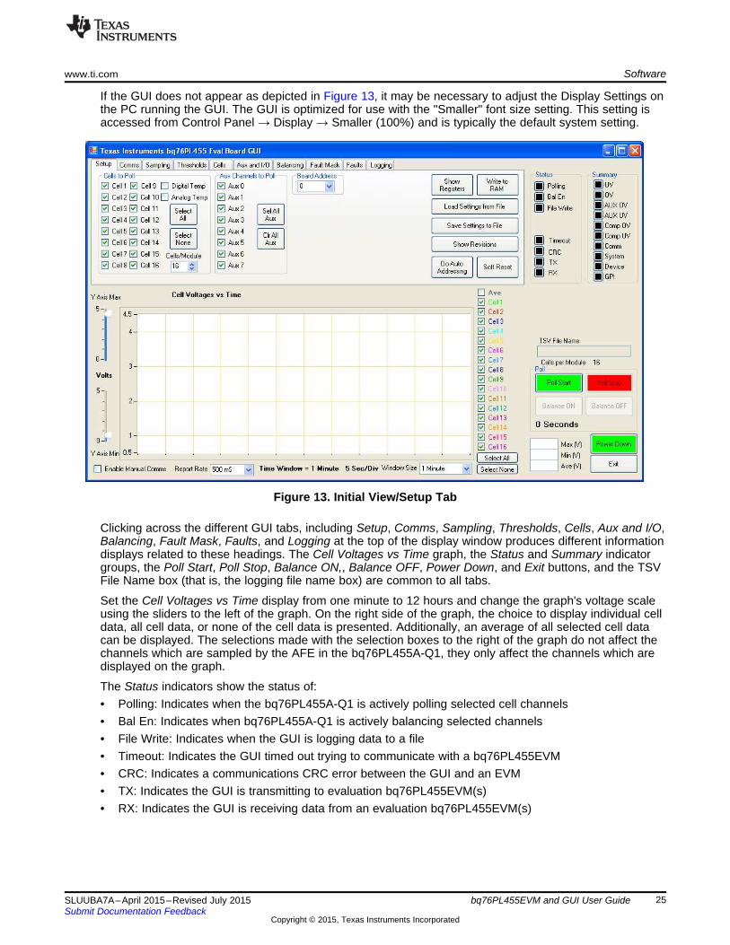
If the GUI does not appear as depicted in Figure 13, it may be necessary to adjust the Display Settings onthe PC running the GUI. The GUI is optimized for use with the "Smaller" font size setting. This setting isaccessed from Control Panel → Display → Smaller (100%) and is typically the default system setting.
Figure 13. Initial View/Setup Tab
Clicking across the different GUI tabs, including Setup, Comms, Sampling, Thresholds, Cells, Aux and I/O,Balancing, Fault Mask, Faults, and Logging at the top of the display window produces different informationdisplays related to these headings. The Cell Voltages vs Time graph, the Status and Summary indicatorgroups, the Poll Start, Poll Stop, Balance ON,, Balance OFF, Power Down, and Exit buttons, and the TSVFile Name box (that is, the logging file name box) are common to all tabs.
Set the Cell Voltages vs Time display from one minute to 12 hours and change the graph's voltage scaleusing the sliders to the left of the graph. On the right side of the graph, the choice to display individual celldata, all cell data, or none of the cell data is presented. Additionally, an average of all selected cell datacan be displayed. The selections made with the selection boxes to the right of the graph do not affect thechannels which are sampled by the AFE in the bq76PL455A-Q1, they only affect the channels which aredisplayed on the graph.
The Status indicators show the status of:• Polling: Indicates when the bq76PL455A-Q1 is actively polling selected cell channels• Bal En: Indicates when bq76PL455A-Q1 is actively balancing selected channels• File Write: Indicates when the GUI is logging data to a file• Timeout: Indicates the GUI timed out trying to communicate with a bq76PL455EVM• CRC: Indicates a communications CRC error between the GUI and an EVM• TX: Indicates the GUI is transmitting to evaluation bq76PL455EVM(s)• RX: Indicates the GUI is receiving data from an evaluation bq76PL455EVM(s)
25SLUUBA7A–April 2015–Revised July 2015 bq76PL455EVM and GUI User GuideSubmit Documentation Feedback
Copyright © 2015, Texas Instruments Incorporated

Software www.ti.com
NOTE: The indicators for Polling, Balancing (Bal En), and File Write turn green when the indicatedactivity is active. The Polling indicator has two states: on (green) and off (black). The FileWrite indicator, however, has three states: green (writing to file, polling active), red (notwriting to file, polling active), and black(off) (not writing to file, polling not active). TheBalancing (Bal En) indicator also has three states: green (balancing on, no fault detected),red (balancing was requested but a fault prevented balancing) and black (off). If timedbalancing was requested, then the Balancing (Bal En) indicator is red once the timed periodexpires to indicate that the timing system is armed for the next timed period.
The Timeout and CRC fault indicators indicate a fault has occurred by turning red. These indicators mustbe cleared manually, once tripped, because they latch the indicated fault.
The TX and RX indicators blink green whenever the indicated activity is active.
The Summary indicators indicate faults, including:• UV: Indicates a cell voltage exceeds the undervoltage threshold• OV: Indicates a cell voltage exceeds the overvoltage threshold• AUX OV: Indicates an AUX input overvoltage threshold is exceeded• AUX UV: Indicates an AUX input undervoltage threshold is exceeded• Comp OV: Indicates a comparator overvoltage threshold is exceeded• Comp UV: Indicates a comparator undervoltage threshold is exceeded• Comm: Indicates a communication fault has occurred• System: Indicates a general system fault is tripped (see the data sheet for a list)• Device: Indicates a fault in the Device Fault register is tripped (see the data sheet)• GPI: Indicates a user-configured input fault condition has been triggered (on the GPI pin)
Clicking any fault indicator clears all faults of the same type. For instance, clicking the UV fault buttonclears all UV faults for all cells. Clear individual cell UV faults by going to the Faults tab, Cell Faults, UVsection and clicking on the desired cell undervoltage fault indicator. Any of the Summary Faults can becleared while polling is active. If the source of the fault persists, then the fault indicator reactivates.
The TSV File Name field shows the file where data is being logged and is set on the Logging tab.
The Poll Start button is used to initiate polling. Polling is stopped using the Poll Stop button. Before pollingis started, set or verify the following parameters on the appropriate tab:1. The number of Cells/Module and Cells to Poll on the Setup tab2. The communications Baud Rate and the Comm Timeout period settings on the Comms tab3. The Initial Sample Delays, Sample Period, OverSample rate, Oversample Method and Aux Sample
period on the Sampling tab4. The Cell Voltage OV and UV limits, Comparator OV and UV limits and Aux Voltage OV and UV limits
on the Thresholds tab5. The desired Fault Masks on the Fault Masks tab6. Clear all faults on Faults tab (verifying proper clearing by issuing a Query All request, and clearing any
latent faults)7. Optionally, use the Log File Path and Name box on the Logging tab to set the storage location for the
Log File (if logging is desired)
The Balance ON button is used to start balancing once the channels to be balanced have been selectedon the Balancing tab and all faults have been cleared on the Faults tab.
NOTE: Cell balancing is not allowed to start if any faults are active, unless those faults have beenmasked or the Continue on Fault checkbox in the Balance Continue box on the Balancingtab is selected. Similarly, if a fault occurs during balancing, balancing stops unless the faulthas been masked. Most, but not all faults can be masked on the Fault Mask tab.
26 bq76PL455EVM and GUI User Guide SLUUBA7A–April 2015–Revised July 2015Submit Documentation Feedback
Copyright © 2015, Texas Instruments Incorporated

www.ti.com Software
The Power Down button powers down the bq76PL455EVM(s). Once powered down, the bq76PL455EVMis powered back up by clicking the Power Up button, which appears in place of the Power Down buttonafter the bq76PL455EVM is powered down.
7.2 Setup TabOn the Setup tab, set the number of cells in the module, which cell and aux channels are monitored,whether internal chip temperatures are monitored, and the bq76PL455EVM address. The Board Addressdrop-down menu is populated with the addresses of all bq76PL455EVMs discovered during the GUI start-up.
If there was a problem with auto-addressing during GUI power up and not all connected bq76PL455EVMswere recognized, reinitiate the search process by clicking the Do Auto Addressing button once theconnection problem has been rectified.
NOTE: Failure to select at least one channel before starting polling results in a GUI error message.
Save the bq76PL455A-Q1 RAM set up data using the Save Settings to File button which saves the data toa file on the PC. These data can later be restored to a bq76PL455EVM using the Load Settings from Filebutton.
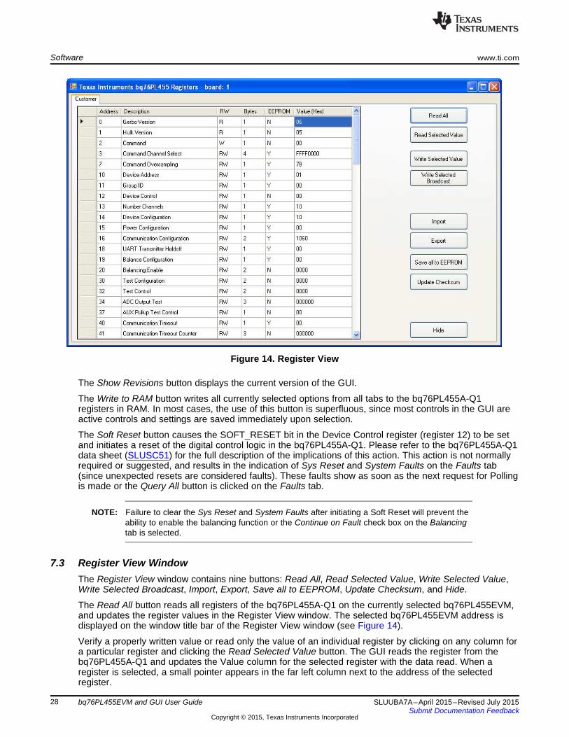
The Show Registers button produces a view, as shown in Figure 14, of the user-configurable registerswhich the GUI is writing to control bq76PL455A-Q1 operation. In the Registers view, values are observedand changed in the registers of the bq76PL455A-Q1. These registers are described in detail in thebq76PL455A-Q1 data sheet (SLUSC51). Register values are read and written from this Register Viewwindow, however, values are only written to RAM and cannot be saved to EEPROM using thebq76PL455EVM GUI. If power is removed from the bq76PL455EVM(s), any changes are lost. For thispurpose, any changes may be saved to and restored from a file using the Export and Import buttons.When importing from a file, values are written to all registers as part of the import process. Someadditional detail regarding the control buttons on this window is provided in the Register View Windowsection of this document.
NOTE: Since changes are made using check boxes and radio buttons in the primary GUI window,registers shown in Register View can change while the Register View window is open. Ifmaking changes in the GUI while the Register View is open, click Read All upon returning tothe Register View window.
27SLUUBA7A–April 2015–Revised July 2015 bq76PL455EVM and GUI User GuideSubmit Documentation Feedback
Copyright © 2015, Texas Instruments Incorporated
Software www.ti.com
Figure 14. Register View
The Show Revisions button displays the current version of the GUI.
The Write to RAM button writes all currently selected options from all tabs to the bq76PL455A-Q1registers in RAM. In most cases, the use of this button is superfluous, since most controls in the GUI areactive controls and settings are saved immediately upon selection.
The Soft Reset button causes the SOFT_RESET bit in the Device Control register (register 12) to be setand initiates a reset of the digital control logic in the bq76PL455A-Q1. Please refer to the bq76PL455A-Q1data sheet (SLUSC51) for the full description of the implications of this action. This action is not normallyrequired or suggested, and results in the indication of Sys Reset and System Faults on the Faults tab(since unexpected resets are considered faults). These faults show as soon as the next request for Pollingis made or the Query All button is clicked on the Faults tab.
NOTE: Failure to clear the Sys Reset and System Faults after initiating a Soft Reset will prevent theability to enable the balancing function or the Continue on Fault check box on the Balancingtab is selected.
7.3 Register View WindowThe Register View window contains nine buttons: Read All, Read Selected Value, Write Selected Value,Write Selected Broadcast, Import, Export, Save all to EEPROM, Update Checksum, and Hide.
The Read All button reads all registers of the bq76PL455A-Q1 on the currently selected bq76PL455EVM,and updates the register values in the Register View window. The selected bq76PL455EVM address isdisplayed on the window title bar of the Register View window (see Figure 14).
Verify a properly written value or read only the value of an individual register by clicking on any column fora particular register and clicking the Read Selected Value button. The GUI reads the register from thebq76PL455A-Q1 and updates the Value column for the selected register with the data read. When aregister is selected, a small pointer appears in the far left column next to the address of the selectedregister.
28 bq76PL455EVM and GUI User Guide SLUUBA7A–April 2015–Revised July 2015Submit Documentation Feedback
Copyright © 2015, Texas Instruments Incorporated
www.ti.com Software
Change this value by clicking on the Value column for a selected register. After doing so, the new value isstored to the RAM copy of the register on the bq76PL455A-Q1 by clicking the Write Selected Registerbutton.
A register value is written to all bq76PL455EVMs in a stack by selecting a register then clicking the WriteSelected Broadcast button.
Once a device has been configured as desired, the register settings are saved to a file using the Exportbutton. The user is prompted for a folder and file name to which to save the register information.
The Import button is used to restore register values to values previously saved to register files using theExport button.
WARNINGThe register files can also be viewed and modified external to theGUI with any text editor, but great care must be exercised whendoing so, since register settings can put the IC into an undesirablestate if mistakes are made in the register files and the data in aregister file overwrites existing register values when imported.
The Save all to EEPROM button saves the values of all the registers which have a correspondingEEPROM location to the non-volatile memory in the bq76PL455A-Q1. Once this is done, the data isstored in the bq76PL455A-Q1 even after the power supply to the TOP pin of the device is removed. If thedevice is reset or power is re-applied after removal, the newly stored settings are loaded into RAM andused thereafter as the new configuration of the device. Due to the limited number of write cyclessupported by the bq76PL455A-Q1, save to EEPROM as seldom as possible. As a reminder to limit thisactivity, a warning pop-up window appears anytime a save to EEPROM is requested. This warningwindow contains the recommended maximum and current write cycle count. An example of this warningwindow is shown in Figure 15.
Figure 15. EEPROM Save Warning
The Update Checksum button is typically not used because the checksum is updated automatically by theGUI for most changes made while in Register View mode and either the Write Selected Value or WriteSelected Broadcast button is clicked. However, in the event of an error or if a manual update is desired,clicking the Update Checksum button causes the value in the Checksum register to be updated to theproper value for the current register settings.
The Hide button, when clicked, closes the Register View window.
29SLUUBA7A–April 2015–Revised July 2015 bq76PL455EVM and GUI User GuideSubmit Documentation Feedback
Copyright © 2015, Texas Instruments Incorporated
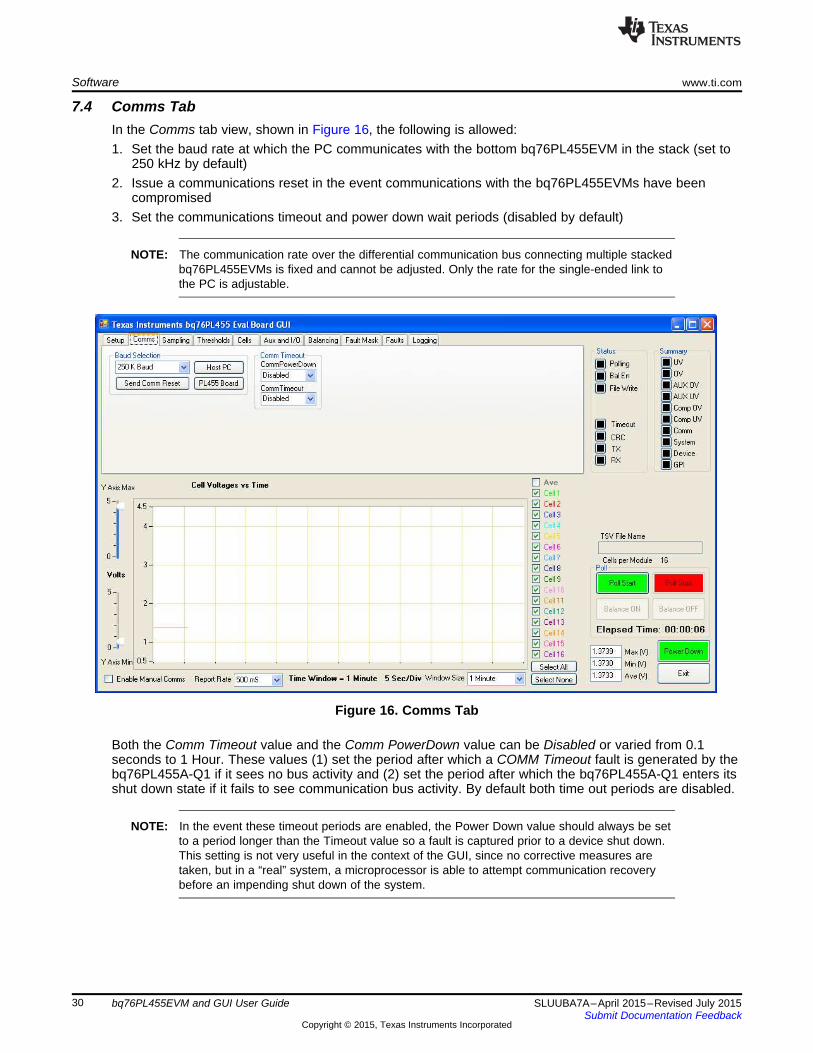
Software www.ti.com
7.4 Comms TabIn the Comms tab view, shown in Figure 16, the following is allowed:1. Set the baud rate at which the PC communicates with the bottom bq76PL455EVM in the stack (set to
250 kHz by default)2. Issue a communications reset in the event communications with the bq76PL455EVMs have been
compromised3. Set the communications timeout and power down wait periods (disabled by default)
NOTE: The communication rate over the differential communication bus connecting multiple stackedbq76PL455EVMs is fixed and cannot be adjusted. Only the rate for the single-ended link tothe PC is adjustable.
Figure 16. Comms Tab
Both the Comm Timeout value and the Comm PowerDown value can be Disabled or varied from 0.1seconds to 1 Hour. These values (1) set the period after which a COMM Timeout fault is generated by thebq76PL455A-Q1 if it sees no bus activity and (2) set the period after which the bq76PL455A-Q1 enters itsshut down state if it fails to see communication bus activity. By default both time out periods are disabled.
NOTE: In the event these timeout periods are enabled, the Power Down value should always be setto a period longer than the Timeout value so a fault is captured prior to a device shut down.This setting is not very useful in the context of the GUI, since no corrective measures aretaken, but in a “real” system, a microprocessor is able to attempt communication recoverybefore an impending shut down of the system.
30 bq76PL455EVM and GUI User Guide SLUUBA7A–April 2015–Revised July 2015Submit Documentation Feedback
Copyright © 2015, Texas Instruments Incorporated
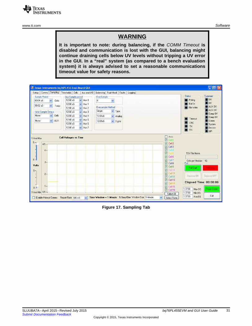
www.ti.com Software
WARNINGIt is important to note: during balancing, if the COMM Timeout isdisabled and communication is lost with the GUI, balancing mightcontinue draining cells below UV levels without tripping a UV errorin the GUI. In a “real” system (as compared to a bench evaluationsystem) it is always advised to set a reasonable communicationstimeout value for safety reasons.
Figure 17. Sampling Tab
31SLUUBA7A–April 2015–Revised July 2015 bq76PL455EVM and GUI User GuideSubmit Documentation Feedback
Copyright © 2015, Texas Instruments Incorporated
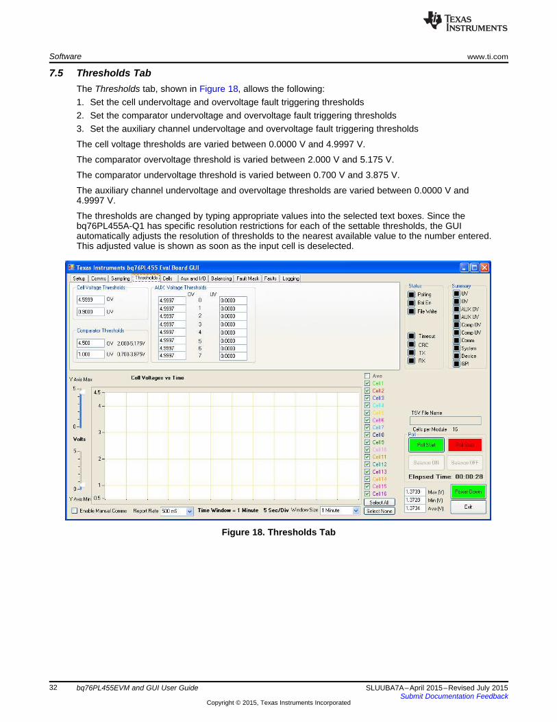
Software www.ti.com
7.5 Thresholds TabThe Thresholds tab, shown in Figure 18, allows the following:1. Set the cell undervoltage and overvoltage fault triggering thresholds2. Set the comparator undervoltage and overvoltage fault triggering thresholds3. Set the auxiliary channel undervoltage and overvoltage fault triggering thresholds
The cell voltage thresholds are varied between 0.0000 V and 4.9997 V.
The comparator overvoltage threshold is varied between 2.000 V and 5.175 V.
The comparator undervoltage threshold is varied between 0.700 V and 3.875 V.
The auxiliary channel undervoltage and overvoltage thresholds are varied between 0.0000 V and4.9997 V.
The thresholds are changed by typing appropriate values into the selected text boxes. Since thebq76PL455A-Q1 has specific resolution restrictions for each of the settable thresholds, the GUIautomatically adjusts the resolution of thresholds to the nearest available value to the number entered.This adjusted value is shown as soon as the input cell is deselected.
Figure 18. Thresholds Tab
32 bq76PL455EVM and GUI User Guide SLUUBA7A–April 2015–Revised July 2015Submit Documentation Feedback
Copyright © 2015, Texas Instruments Incorporated
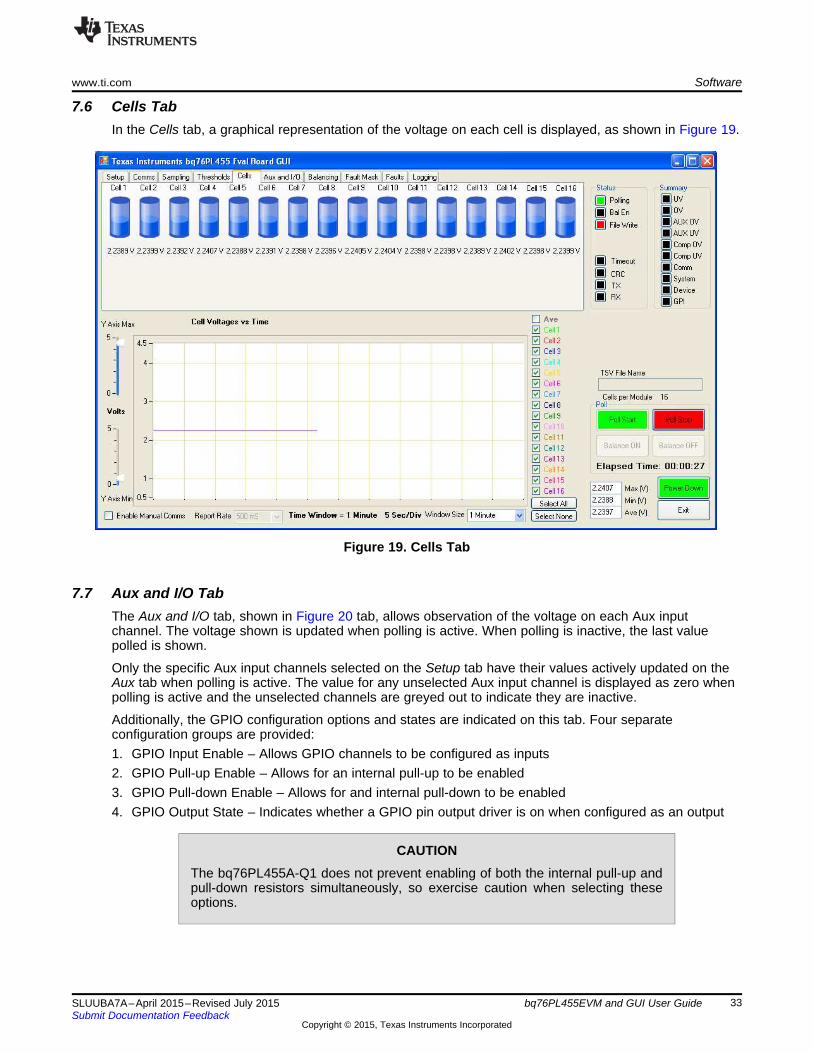
www.ti.com Software
7.6 Cells TabIn the Cells tab, a graphical representation of the voltage on each cell is displayed, as shown in Figure 19.
Figure 19. Cells Tab
7.7 Aux and I/O TabThe Aux and I/O tab, shown in Figure 20 tab, allows observation of the voltage on each Aux inputchannel. The voltage shown is updated when polling is active. When polling is inactive, the last valuepolled is shown.
Only the specific Aux input channels selected on the Setup tab have their values actively updated on theAux tab when polling is active. The value for any unselected Aux input channel is displayed as zero whenpolling is active and the unselected channels are greyed out to indicate they are inactive.
Additionally, the GPIO configuration options and states are indicated on this tab. Four separateconfiguration groups are provided:1. GPIO Input Enable – Allows GPIO channels to be configured as inputs2. GPIO Pull-up Enable – Allows for an internal pull-up to be enabled3. GPIO Pull-down Enable – Allows for and internal pull-down to be enabled4. GPIO Output State – Indicates whether a GPIO pin output driver is on when configured as an output
CAUTIONThe bq76PL455A-Q1 does not prevent enabling of both the internal pull-up andpull-down resistors simultaneously, so exercise caution when selecting theseoptions.
33SLUUBA7A–April 2015–Revised July 2015 bq76PL455EVM and GUI User GuideSubmit Documentation Feedback
Copyright © 2015, Texas Instruments Incorporated
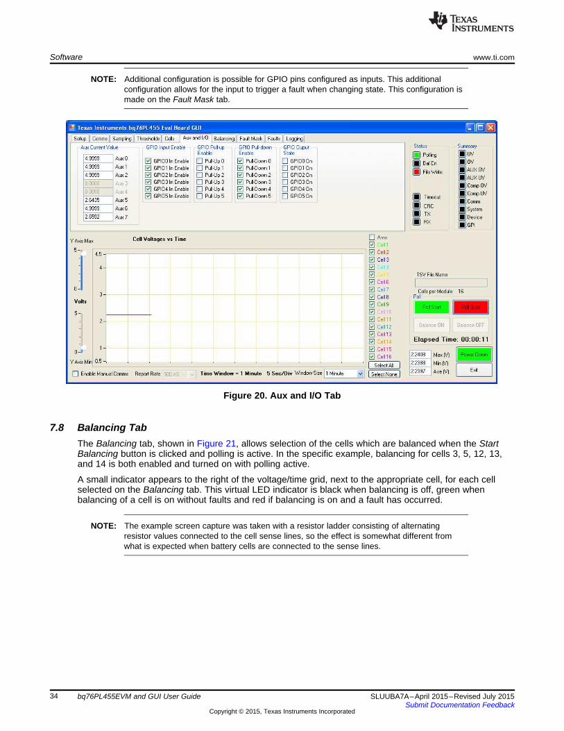
Software www.ti.com
NOTE: Additional configuration is possible for GPIO pins configured as inputs. This additionalconfiguration allows for the input to trigger a fault when changing state. This configuration ismade on the Fault Mask tab.
Figure 20. Aux and I/O Tab
7.8 Balancing TabThe Balancing tab, shown in Figure 21, allows selection of the cells which are balanced when the StartBalancing button is clicked and polling is active. In the specific example, balancing for cells 3, 5, 12, 13,and 14 is both enabled and turned on with polling active.
A small indicator appears to the right of the voltage/time grid, next to the appropriate cell, for each cellselected on the Balancing tab. This virtual LED indicator is black when balancing is off, green whenbalancing of a cell is on without faults and red if balancing is on and a fault has occurred.
NOTE: The example screen capture was taken with a resistor ladder consisting of alternatingresistor values connected to the cell sense lines, so the effect is somewhat different fromwhat is expected when battery cells are connected to the sense lines.
34 bq76PL455EVM and GUI User Guide SLUUBA7A–April 2015–Revised July 2015Submit Documentation Feedback
Copyright © 2015, Texas Instruments Incorporated
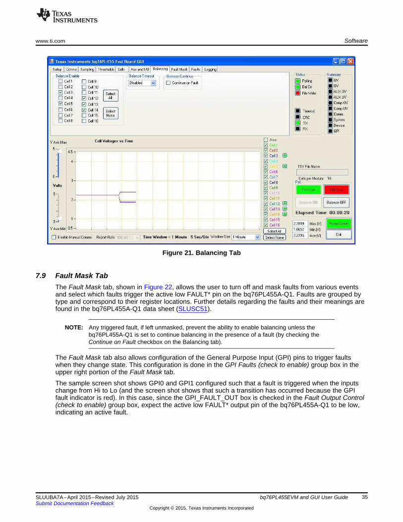
www.ti.com Software
Figure 21. Balancing Tab
7.9 Fault Mask TabThe Fault Mask tab, shown in Figure 22, allows the user to turn off and mask faults from various eventsand select which faults trigger the active low FAULT* pin on the bq76PL455A-Q1. Faults are grouped bytype and correspond to their register locations. Further details regarding the faults and their meanings arefound in the bq76PL455A-Q1 data sheet (SLUSC51).
NOTE: Any triggered fault, if left unmasked, prevent the ability to enable balancing unless thebq76PL455A-Q1 is set to continue balancing in the presence of a fault (by checking theContinue on Fault checkbox on the Balancing tab).
The Fault Mask tab also allows configuration of the General Purpose Input (GPI) pins to trigger faultswhen they change state. This configuration is done in the GPI Faults (check to enable) group box in theupper right portion of the Fault Mask tab.
The sample screen shot shows GPI0 and GPI1 configured such that a fault is triggered when the inputschange from Hi to Lo (and the screen shot shows that such a transition has occurred because the GPIfault indicator is red). In this case, since the GPI_FAULT_OUT box is checked in the Fault Output Control(check to enable) group box, expect the active low FAULT* output pin of the bq76PL455A-Q1 to be low,indicating an active fault.
35SLUUBA7A–April 2015–Revised July 2015 bq76PL455EVM and GUI User GuideSubmit Documentation Feedback
Copyright © 2015, Texas Instruments Incorporated
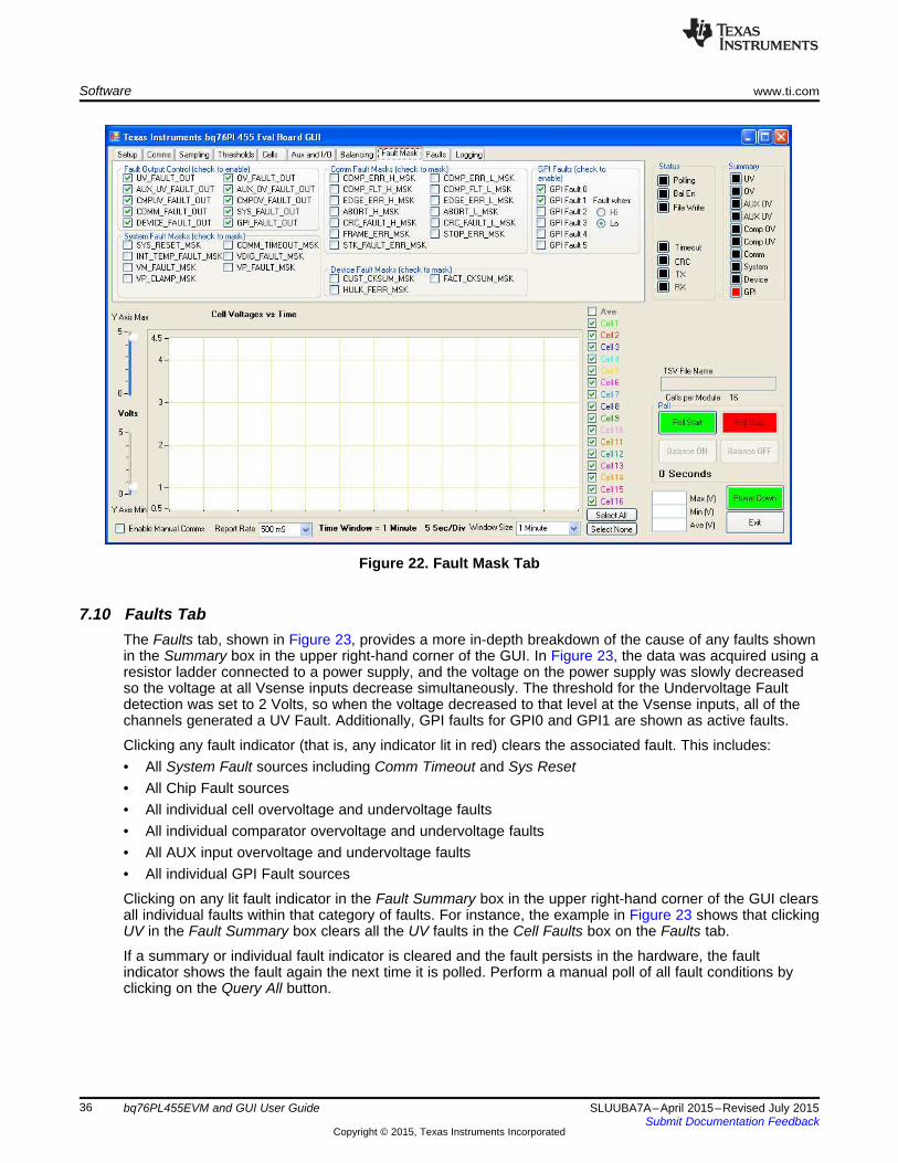
Software www.ti.com
Figure 22. Fault Mask Tab
7.10 Faults TabThe Faults tab, shown in Figure 23, provides a more in-depth breakdown of the cause of any faults shownin the Summary box in the upper right-hand corner of the GUI. In Figure 23, the data was acquired using aresistor ladder connected to a power supply, and the voltage on the power supply was slowly decreasedso the voltage at all Vsense inputs decrease simultaneously. The threshold for the Undervoltage Faultdetection was set to 2 Volts, so when the voltage decreased to that level at the Vsense inputs, all of thechannels generated a UV Fault. Additionally, GPI faults for GPI0 and GPI1 are shown as active faults.
Clicking any fault indicator (that is, any indicator lit in red) clears the associated fault. This includes:• All System Fault sources including Comm Timeout and Sys Reset• All Chip Fault sources• All individual cell overvoltage and undervoltage faults• All individual comparator overvoltage and undervoltage faults• All AUX input overvoltage and undervoltage faults• All individual GPI Fault sources
Clicking on any lit fault indicator in the Fault Summary box in the upper right-hand corner of the GUI clearsall individual faults within that category of faults. For instance, the example in Figure 23 shows that clickingUV in the Fault Summary box clears all the UV faults in the Cell Faults box on the Faults tab.
If a summary or individual fault indicator is cleared and the fault persists in the hardware, the faultindicator shows the fault again the next time it is polled. Perform a manual poll of all fault conditions byclicking on the Query All button.
36 bq76PL455EVM and GUI User Guide SLUUBA7A–April 2015–Revised July 2015Submit Documentation Feedback
Copyright © 2015, Texas Instruments Incorporated
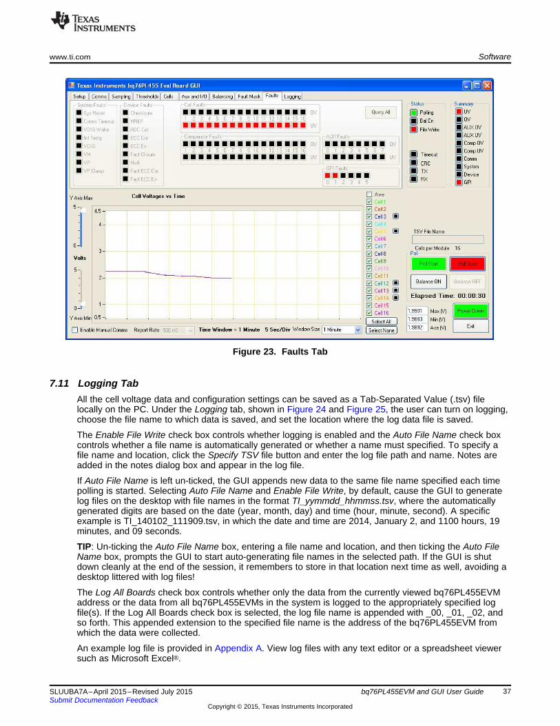
www.ti.com Software
Figure 23. Faults Tab
7.11 Logging TabAll the cell voltage data and configuration settings can be saved as a Tab-Separated Value (.tsv) filelocally on the PC. Under the Logging tab, shown in Figure 24 and Figure 25, the user can turn on logging,choose the file name to which data is saved, and set the location where the log data file is saved.
The Enable File Write check box controls whether logging is enabled and the Auto File Name check boxcontrols whether a file name is automatically generated or whether a name must specified. To specify afile name and location, click the Specify TSV file button and enter the log file path and name. Notes areadded in the notes dialog box and appear in the log file.
If Auto File Name is left un-ticked, the GUI appends new data to the same file name specified each timepolling is started. Selecting Auto File Name and Enable File Write, by default, cause the GUI to generatelog files on the desktop with file names in the format TI_yymmdd_hhmmss.tsv, where the automaticallygenerated digits are based on the date (year, month, day) and time (hour, minute, second). A specificexample is TI_140102_111909.tsv, in which the date and time are 2014, January 2, and 1100 hours, 19minutes, and 09 seconds.
TIP: Un-ticking the Auto File Name box, entering a file name and location, and then ticking the Auto FileName box, prompts the GUI to start auto-generating file names in the selected path. If the GUI is shutdown cleanly at the end of the session, it remembers to store in that location next time as well, avoiding adesktop littered with log files!
The Log All Boards check box controls whether only the data from the currently viewed bq76PL455EVMaddress or the data from all bq76PL455EVMs in the system is logged to the appropriately specified logfile(s). If the Log All Boards check box is selected, the log file name is appended with _00, _01, _02, andso forth. This appended extension to the specified file name is the address of the bq76PL455EVM fromwhich the data were collected.
An example log file is provided in Appendix A. View log files with any text editor or a spreadsheet viewersuch as Microsoft Excel®.
37SLUUBA7A–April 2015–Revised July 2015 bq76PL455EVM and GUI User GuideSubmit Documentation Feedback
Copyright © 2015, Texas Instruments Incorporated
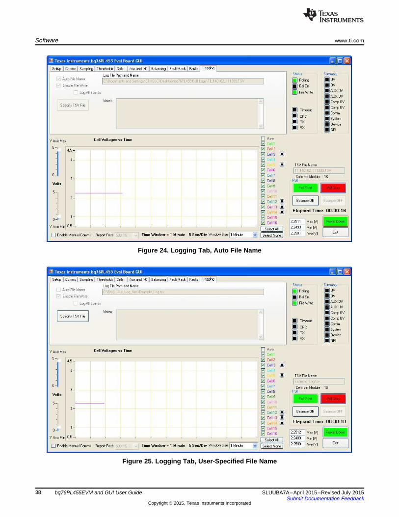
Software www.ti.com
Figure 24. Logging Tab, Auto File Name
Figure 25. Logging Tab, User-Specified File Name
38 bq76PL455EVM and GUI User Guide SLUUBA7A–April 2015–Revised July 2015Submit Documentation Feedback
Copyright © 2015, Texas Instruments Incorporated
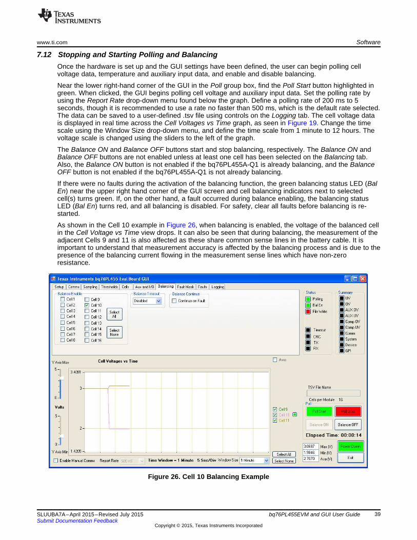
www.ti.com Software
7.12 Stopping and Starting Polling and BalancingOnce the hardware is set up and the GUI settings have been defined, the user can begin polling cellvoltage data, temperature and auxiliary input data, and enable and disable balancing.
Near the lower right-hand corner of the GUI in the Poll group box, find the Poll Start button highlighted ingreen. When clicked, the GUI begins polling cell voltage and auxiliary input data. Set the polling rate byusing the Report Rate drop-down menu found below the graph. Define a polling rate of 200 ms to 5seconds, though it is recommended to use a rate no faster than 500 ms, which is the default rate selected.The data can be saved to a user-defined .tsv file using controls on the Logging tab. The cell voltage datais displayed in real time across the Cell Voltages vs Time graph, as seen in Figure 19. Change the timescale using the Window Size drop-down menu, and define the time scale from 1 minute to 12 hours. Thevoltage scale is changed using the sliders to the left of the graph.
The Balance ON and Balance OFF buttons start and stop balancing, respectively. The Balance ON andBalance OFF buttons are not enabled unless at least one cell has been selected on the Balancing tab.Also, the Balance ON button is not enabled if the bq76PL455A-Q1 is already balancing, and the BalanceOFF button is not enabled if the bq76PL455A-Q1 is not already balancing.
If there were no faults during the activation of the balancing function, the green balancing status LED (BalEn) near the upper right hand corner of the GUI screen and cell balancing indicators next to selectedcell(s) turns green. If, on the other hand, a fault occurred during balance enabling, the balancing statusLED (Bal En) turns red, and all balancing is disabled. For safety, clear all faults before balancing is re-started.
As shown in the Cell 10 example in Figure 26, when balancing is enabled, the voltage of the balanced cellin the Cell Voltage vs Time view drops. It can also be seen that during balancing, the measurement of theadjacent Cells 9 and 11 is also affected as these share common sense lines in the battery cable. It isimportant to understand that measurement accuracy is affected by the balancing process and is due to thepresence of the balancing current flowing in the measurement sense lines which have non-zeroresistance.
Figure 26. Cell 10 Balancing Example
39SLUUBA7A–April 2015–Revised July 2015 bq76PL455EVM and GUI User GuideSubmit Documentation Feedback
Copyright © 2015, Texas Instruments Incorporated
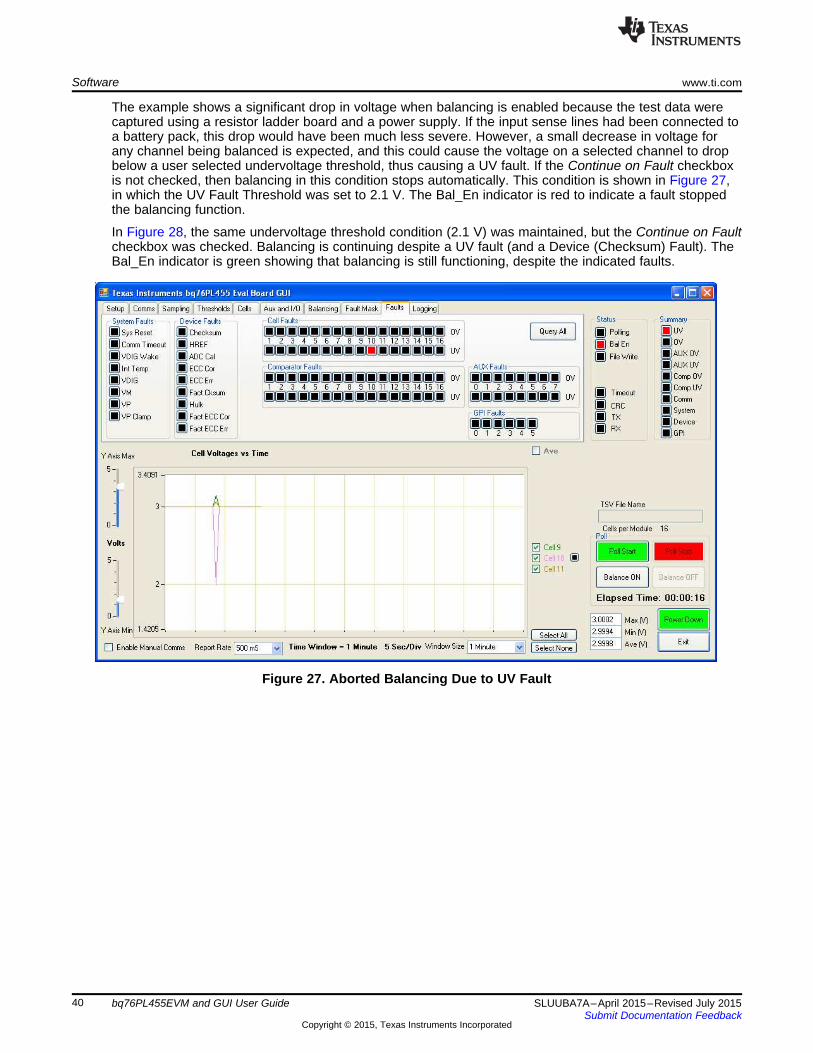
Software www.ti.com
The example shows a significant drop in voltage when balancing is enabled because the test data werecaptured using a resistor ladder board and a power supply. If the input sense lines had been connected toa battery pack, this drop would have been much less severe. However, a small decrease in voltage forany channel being balanced is expected, and this could cause the voltage on a selected channel to dropbelow a user selected undervoltage threshold, thus causing a UV fault. If the Continue on Fault checkboxis not checked, then balancing in this condition stops automatically. This condition is shown in Figure 27,in which the UV Fault Threshold was set to 2.1 V. The Bal_En indicator is red to indicate a fault stoppedthe balancing function.
In Figure 28, the same undervoltage threshold condition (2.1 V) was maintained, but the Continue on Faultcheckbox was checked. Balancing is continuing despite a UV fault (and a Device (Checksum) Fault). TheBal_En indicator is green showing that balancing is still functioning, despite the indicated faults.
Figure 27. Aborted Balancing Due to UV Fault
40 bq76PL455EVM and GUI User Guide SLUUBA7A–April 2015–Revised July 2015Submit Documentation Feedback
Copyright © 2015, Texas Instruments Incorporated
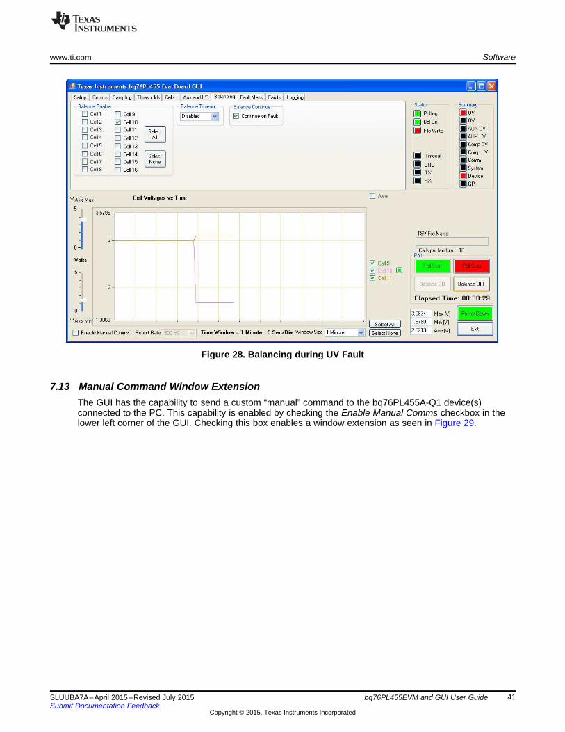
www.ti.com Software
Figure 28. Balancing during UV Fault
7.13 Manual Command Window ExtensionThe GUI has the capability to send a custom “manual” command to the bq76PL455A-Q1 device(s)connected to the PC. This capability is enabled by checking the Enable Manual Comms checkbox in thelower left corner of the GUI. Checking this box enables a window extension as seen in Figure 29.
41SLUUBA7A–April 2015–Revised July 2015 bq76PL455EVM and GUI User GuideSubmit Documentation Feedback
Copyright © 2015, Texas Instruments Incorporated
Software www.ti.com
Figure 29. Manual Communications Window
7.14 Sections of the Manual Command Window ExtensionThe Manual Comms window extension is broken into four sections. The four sections are:1. The Send Command window and the associated Calc CRC check box and Send button2. The Command window and the associated menu bar with the Clear, Save, Load, Edit, ClrComm, Run
and Help buttons3. The Script buttons4. The Packets Logged window and its associated menu bar with the Clear and Save buttons
The functions enabled by this window extension are powerful. Proper use of the functions require athorough understanding of the messaging protocol employed by the bq76PL455A-Q1. For this reason,read and understand the bq76PL455A-Q1 data sheet’s (SLUSC51) description of the message packetformat before using the functions in this window extension.
42 bq76PL455EVM and GUI User Guide SLUUBA7A–April 2015–Revised July 2015Submit Documentation Feedback
Copyright © 2015, Texas Instruments Incorporated
www.ti.com Software
CAUTIONIf improperly formatted messages are sent to one or more bq76PL455A-Q1devices using this interface, then it is possible to inadvertently change thebehavior of one or more devices! Exercise great care when sending commandsto connected devices.
7.14.1 The Send Command Window SectionA command is entered as a string of hexadecimal characters using the Send Command window. Thecommand is later sent to one or more bq76PL455A-Q1 devices. Each command message string is madeup of a header byte, several data bytes and two CRC bytes. To make it easier to form command strings,the GUI can calculate the CRC bytes if the Calc CRC box next to the Send Command window is checked.
Clicking the Send button next to the Send Command window moves the command in the Send Commandwindow into the larger Command window and immediately sends the command. When the GUI is initiallystarted, an example command string is loaded into the Send Command window. This example command(89 00 00 0D 00, without CRC) requests the data in register 13 from the first bq76PL455A-Q1 connectedto the GUI (that is, the device with Device ID Address 0). Since the Calc CRC checkbox is checked bydefault, the command has the CRC bytes added to the command string before it is sent (that is, 89 00 000D 00 D9 4F).
7.14.2 The Command Window SectionAny command scheduled to be sent to the device(s) connected to the GUI is listed in the Commandwindow. Commands listed in this window can come from either the Send Command window or a script file(explained in Section 7.14.3).
NOTE: Commands listed in the Command window have not necessarily been sent to the device. Ifthe source of the command is the Send Command window, then the command has beensent. If the source of the command(s) is a script file, then the command(s) are not sent untilthe Run button to the right of the Command window is clicked.
Multiple commands are transferred to the Command window. These commands remain in the Commandwindow until they are erased by clicking the Clear button to the right of the Command window. This is aconvenient method for building scripts from within the GUI. Once one or more commands have beenrecorded in the Command window, the command(s) can be saved to a script file by clicking the Savebutton to the right of the Command window. Commands are saved to script files in plain text, so these filescan be readily edited using any desired text editor. Reload and run script files later by clicking the Loadand Run buttons, respectively.
43SLUUBA7A–April 2015–Revised July 2015 bq76PL455EVM and GUI User GuideSubmit Documentation Feedback
Copyright © 2015, Texas Instruments Incorporated
Software www.ti.com
Figure 30 through Figure 34 demonstrate how to load and run a previously saved script file.
Figure 30. Ready to Load Previously Saved Script
44 bq76PL455EVM and GUI User Guide SLUUBA7A–April 2015–Revised July 2015Submit Documentation Feedback
Copyright © 2015, Texas Instruments Incorporated
www.ti.com Software
Clicking the Load button brings up a script selection window. The window defaults to the last useddirectory, but this directory can be changed to any desired directory. In the example in Figure 31, thescript with the filename, “Sample – Broadcast Sample all Boards.txt” is selected. antigravity
Figure 31. Load Script Selection Window
45SLUUBA7A–April 2015–Revised July 2015 bq76PL455EVM and GUI User GuideSubmit Documentation Feedback
Copyright © 2015, Texas Instruments Incorporated
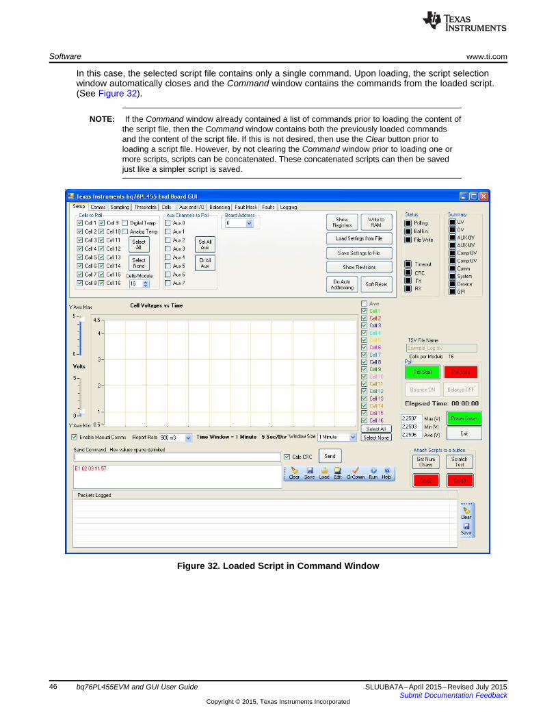
Software www.ti.com
In this case, the selected script file contains only a single command. Upon loading, the script selectionwindow automatically closes and the Command window contains the commands from the loaded script.(See Figure 32).
NOTE: If the Command window already contained a list of commands prior to loading the content ofthe script file, then the Command window contains both the previously loaded commandsand the content of the script file. If this is not desired, then use the Clear button prior toloading a script file. However, by not clearing the Command window prior to loading one ormore scripts, scripts can be concatenated. These concatenated scripts can then be savedjust like a simpler script is saved.
Figure 32. Loaded Script in Command Window
46 bq76PL455EVM and GUI User Guide SLUUBA7A–April 2015–Revised July 2015Submit Documentation Feedback
Copyright © 2015, Texas Instruments Incorporated
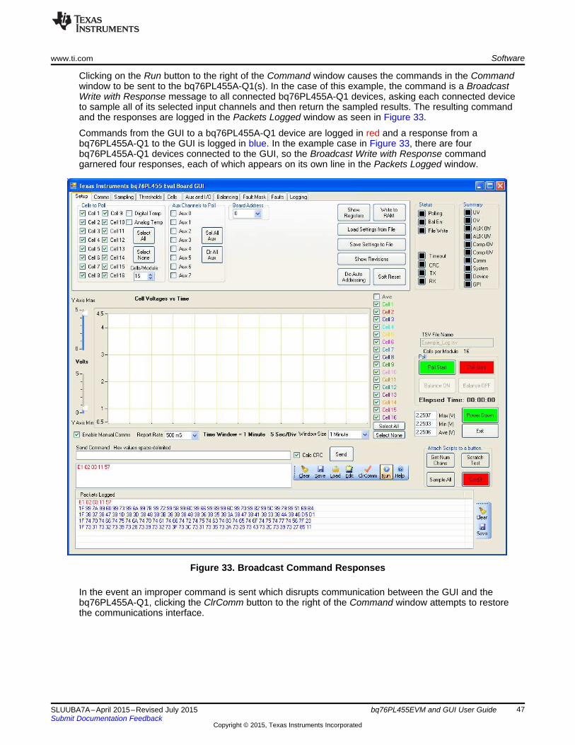
www.ti.com Software
Clicking on the Run button to the right of the Command window causes the commands in the Commandwindow to be sent to the bq76PL455A-Q1(s). In the case of this example, the command is a BroadcastWrite with Response message to all connected bq76PL455A-Q1 devices, asking each connected deviceto sample all of its selected input channels and then return the sampled results. The resulting commandand the responses are logged in the Packets Logged window as seen in Figure 33.
Commands from the GUI to a bq76PL455A-Q1 device are logged in red and a response from abq76PL455A-Q1 to the GUI is logged in blue. In the example case in Figure 33, there are fourbq76PL455A-Q1 devices connected to the GUI, so the Broadcast Write with Response commandgarnered four responses, each of which appears on its own line in the Packets Logged window.
Figure 33. Broadcast Command Responses
In the event an improper command is sent which disrupts communication between the GUI and thebq76PL455A-Q1, clicking the ClrComm button to the right of the Command window attempts to restorethe communications interface.
47SLUUBA7A–April 2015–Revised July 2015 bq76PL455EVM and GUI User GuideSubmit Documentation Feedback
Copyright © 2015, Texas Instruments Incorporated
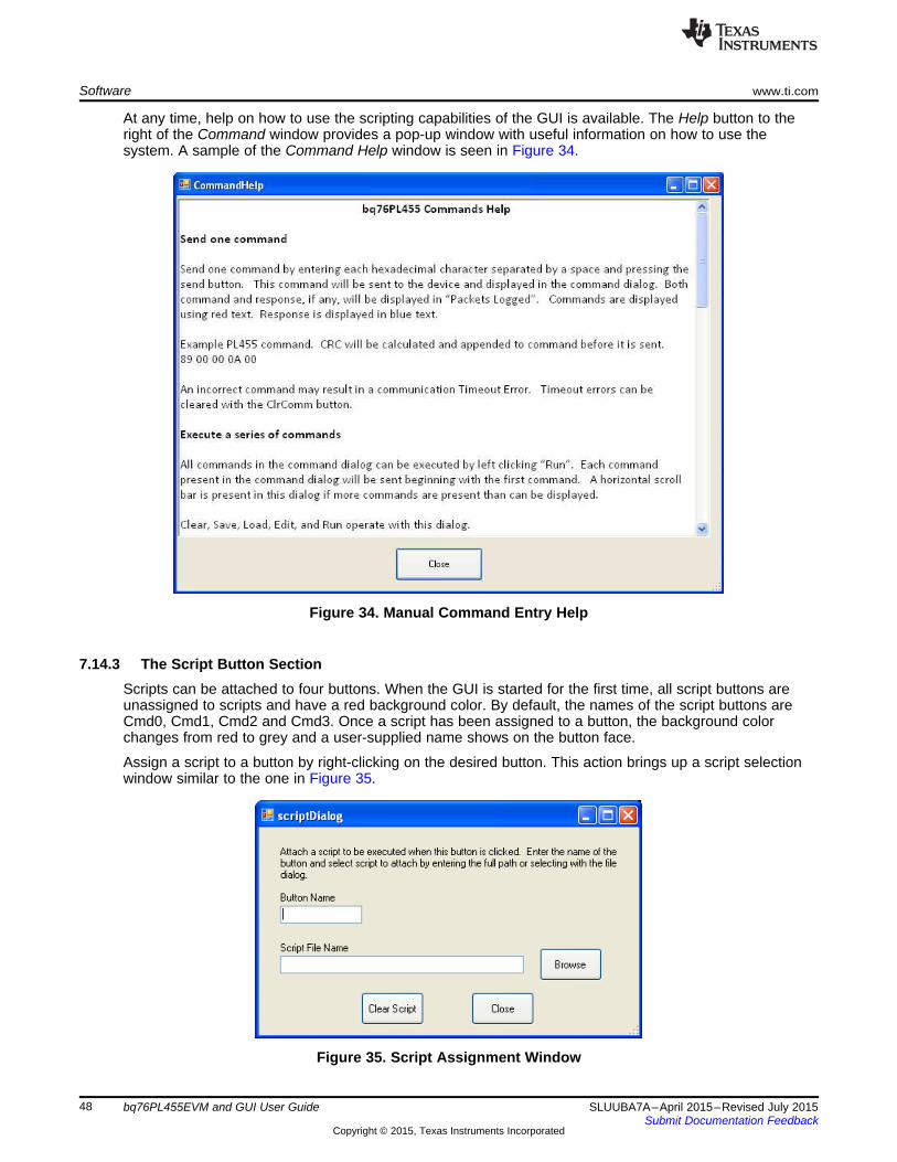
Software www.ti.com
At any time, help on how to use the scripting capabilities of the GUI is available. The Help button to theright of the Command window provides a pop-up window with useful information on how to use thesystem. A sample of the Command Help window is seen in Figure 34.
Figure 34. Manual Command Entry Help
7.14.3 The Script Button SectionScripts can be attached to four buttons. When the GUI is started for the first time, all script buttons areunassigned to scripts and have a red background color. By default, the names of the script buttons areCmd0, Cmd1, Cmd2 and Cmd3. Once a script has been assigned to a button, the background colorchanges from red to grey and a user-supplied name shows on the button face.
Assign a script to a button by right-clicking on the desired button. This action brings up a script selectionwindow similar to the one in Figure 35.
Figure 35. Script Assignment Window
48 bq76PL455EVM and GUI User Guide SLUUBA7A–April 2015–Revised July 2015Submit Documentation Feedback
Copyright © 2015, Texas Instruments Incorporated
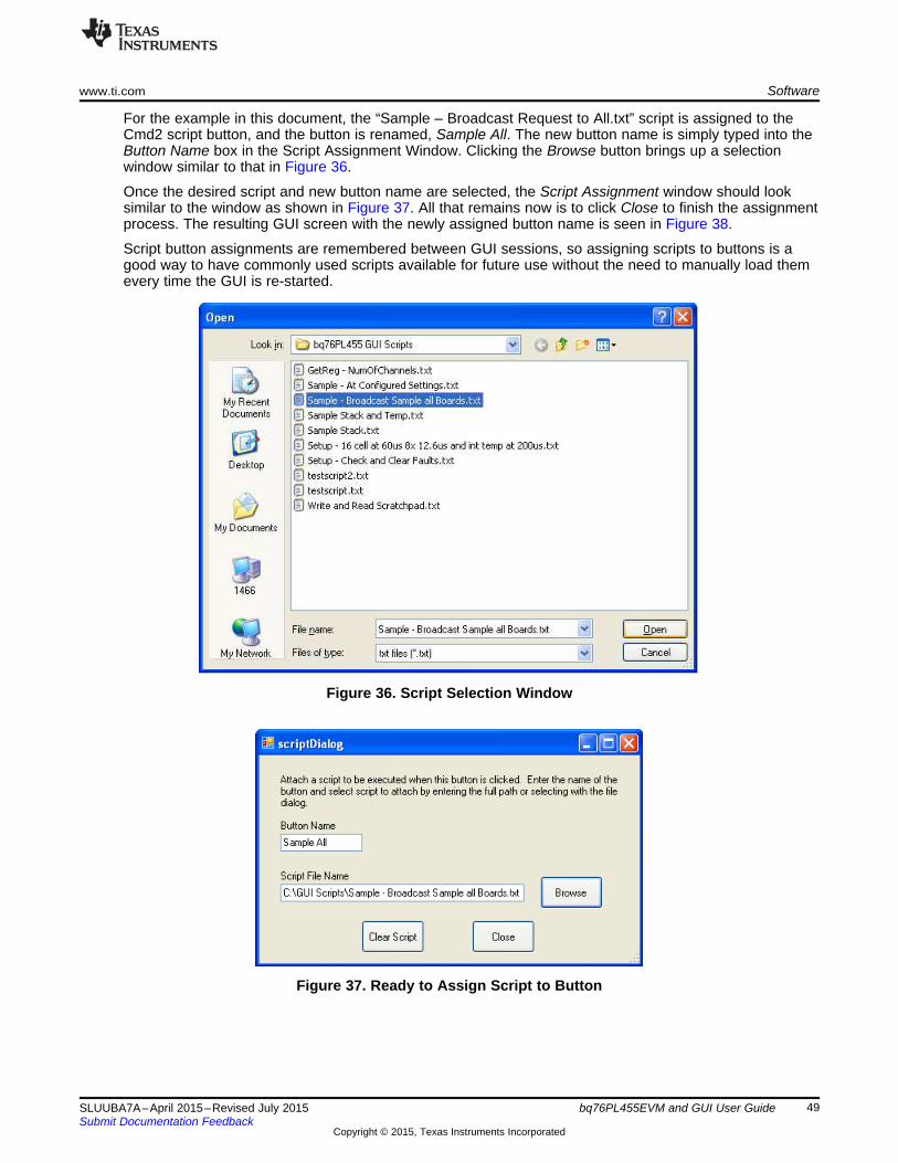
www.ti.com Software
For the example in this document, the “Sample – Broadcast Request to All.txt” script is assigned to theCmd2 script button, and the button is renamed, Sample All. The new button name is simply typed into theButton Name box in the Script Assignment Window. Clicking the Browse button brings up a selectionwindow similar to that in Figure 36.
Once the desired script and new button name are selected, the Script Assignment window should looksimilar to the window as shown in Figure 37. All that remains now is to click Close to finish the assignmentprocess. The resulting GUI screen with the newly assigned button name is seen in Figure 38.
Script button assignments are remembered between GUI sessions, so assigning scripts to buttons is agood way to have commonly used scripts available for future use without the need to manually load themevery time the GUI is re-started.
Figure 36. Script Selection Window
Figure 37. Ready to Assign Script to Button
49SLUUBA7A–April 2015–Revised July 2015 bq76PL455EVM and GUI User GuideSubmit Documentation Feedback
Copyright © 2015, Texas Instruments Incorporated
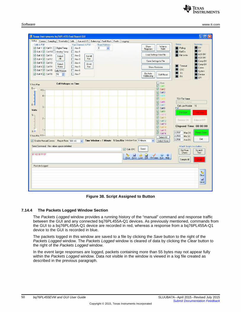
Software www.ti.com
Figure 38. Script Assigned to Button
7.14.4 The Packets Logged Window SectionThe Packets Logged window provides a running history of the “manual” command and response trafficbetween the GUI and any connected bq76PL455A-Q1 devices. As previously mentioned, commands fromthe GUI to a bq76PL455A-Q1 device are recorded in red, whereas a response from a bq76PL455A-Q1device to the GUI is recorded in blue.
The packets logged in this window are saved to a file by clicking the Save button to the right of thePackets Logged window. The Packets Logged window is cleared of data by clicking the Clear button tothe right of the Packets Logged window.
In the event large responses are logged, packets containing more than 55 bytes may not appear fullywithin the Packets Logged window. Data not visible in the window is viewed in a log file created asdescribed in the previous paragraph.
50 bq76PL455EVM and GUI User Guide SLUUBA7A–April 2015–Revised July 2015Submit Documentation Feedback
Copyright © 2015, Texas Instruments Incorporated
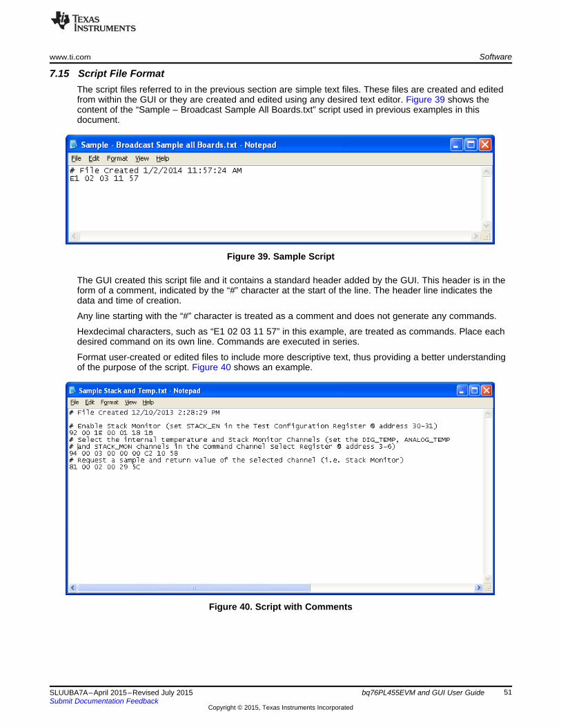
www.ti.com Software
7.15 Script File FormatThe script files referred to in the previous section are simple text files. These files are created and editedfrom within the GUI or they are created and edited using any desired text editor. Figure 39 shows thecontent of the “Sample – Broadcast Sample All Boards.txt” script used in previous examples in thisdocument.
Figure 39. Sample Script
The GUI created this script file and it contains a standard header added by the GUI. This header is in theform of a comment, indicated by the “#” character at the start of the line. The header line indicates thedata and time of creation.
Any line starting with the “#” character is treated as a comment and does not generate any commands.
Hexdecimal characters, such as “E1 02 03 11 57” in this example, are treated as commands. Place eachdesired command on its own line. Commands are executed in series.
Format user-created or edited files to include more descriptive text, thus providing a better understandingof the purpose of the script. Figure 40 shows an example.
Figure 40. Script with Comments
51SLUUBA7A–April 2015–Revised July 2015 bq76PL455EVM and GUI User GuideSubmit Documentation Feedback
Copyright © 2015, Texas Instruments Incorporated
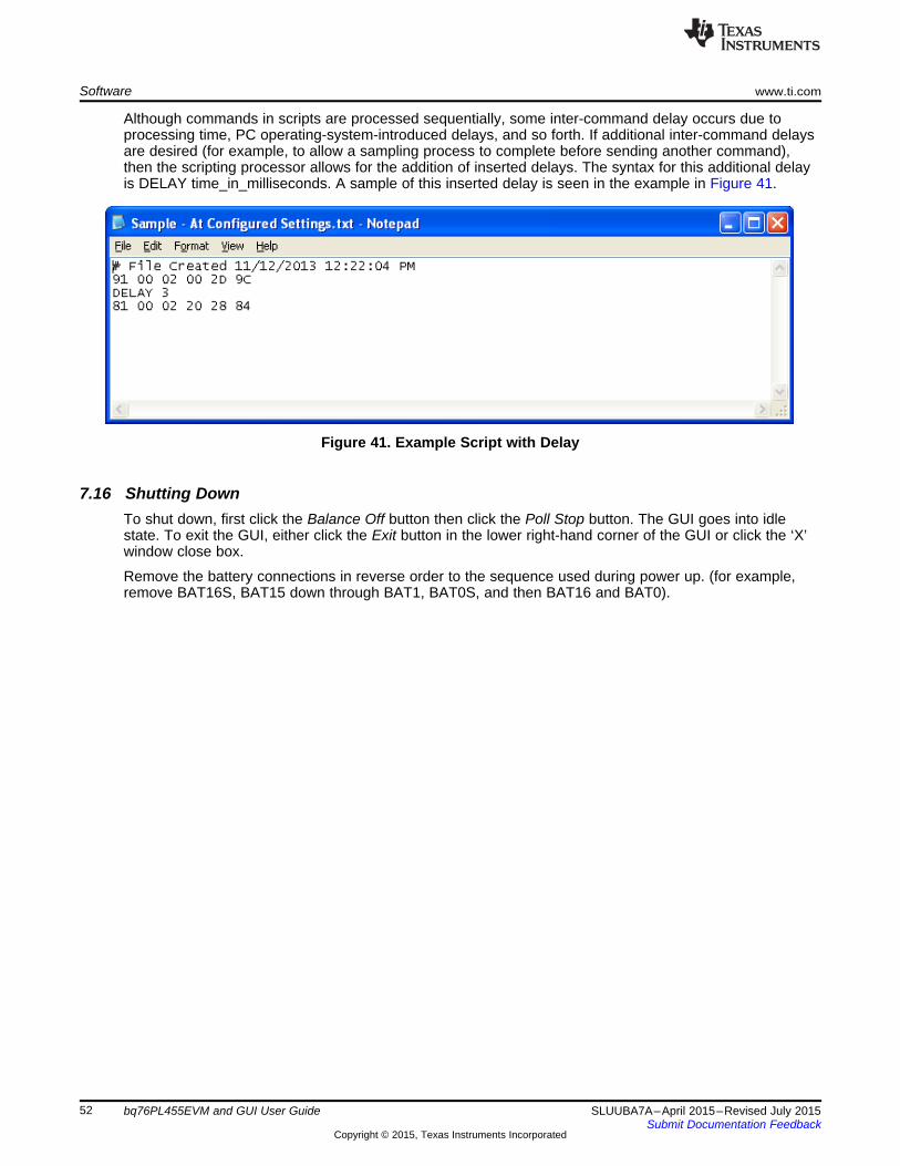
Software www.ti.com
Although commands in scripts are processed sequentially, some inter-command delay occurs due toprocessing time, PC operating-system-introduced delays, and so forth. If additional inter-command delaysare desired (for example, to allow a sampling process to complete before sending another command),then the scripting processor allows for the addition of inserted delays. The syntax for this additional delayis DELAY time_in_milliseconds. A sample of this inserted delay is seen in the example in Figure 41.
Figure 41. Example Script with Delay
7.16 Shutting DownTo shut down, first click the Balance Off button then click the Poll Stop button. The GUI goes into idlestate. To exit the GUI, either click the Exit button in the lower right-hand corner of the GUI or click the ‘X’window close box.
Remove the battery connections in reverse order to the sequence used during power up. (for example,remove BAT16S, BAT15 down through BAT1, BAT0S, and then BAT16 and BAT0).
52 bq76PL455EVM and GUI User Guide SLUUBA7A–April 2015–Revised July 2015Submit Documentation Feedback
Copyright © 2015, Texas Instruments Incorporated
Appendix ASLUUBA7A–April 2015–Revised July 2015
Log Files
A.1 Log File InformationEach log file produced by the GUI contains information for a single evaluation module in the stack ofbq76PL455EVMs connected to the host controller PC. This Appendix section provides detail and sampledata for a log file produced by the GUI.
A log file produced by the GUI is in .tsv format. The name for this file may be chosen, or it canautomatically be generated by the GUI. If the name user-created, provide a full path and name for the file.If the GUI automatically generates the file name, the format of the name is TI_yymmdd_hhmmss.tsv, andthe file is stored in the default directory specified upon the initial GUI installation. The dynamic portions ofthe automatic GUI-generated file name have the following meanings:• yy: last two digits of the year in which file was generated• mm: two-digit month in which the file was generated• dd: two-digit day of the month on which file was generated• hh: hour, in 24-hour format, at which logging began• mm: minute at which the logging began• ss: second at which the logging began
53SLUUBA7A–April 2015–Revised July 2015 Log FilesSubmit Documentation Feedback
Copyright © 2015, Texas Instruments Incorporated
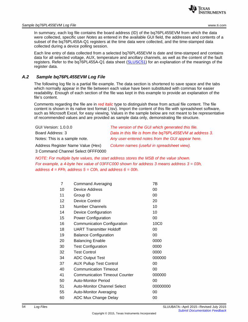
Sample bq76PL455EVM Log File www.ti.com
In summary, each log file contains the board address (ID) of the bq76PL455EVM from which the datawere collected, specific user Notes as entered in the available GUI field, the addresses and contents of asubset of the bq76PL455A-Q1 registers at the time data were collected, and the time-stamped datacollected during a device polling session.
Each line entry of data collected from a selected bq76PL455EVM is date and time-stamped and containsdata for all selected voltage, AUX, temperature and ancillary channels, as well as the content of the faultregisters. Refer to the bq76PL455A-Q1 data sheet (SLUSC51) for an explanation of the meanings of theregister data.
A.2 Sample bq76PL455EVM Log FileThe following log file is a partial file example. The data section is shortened to save space and the tabswhich normally appear in the file between each value have been substituted with commas for easierreadability. Enough of each section of the file was kept in this example to provide an explanation of thefile’s content.
Comments regarding the file are in red italic type to distinguish these from actual file content. The filecontent is shown in its native text format (.tsv). Import the content of this file with spreadsheet software,such as Microsoft Excel, for easy viewing. Values in the sample below are not meant to be representativeof recommended values and are provided as sample data only, demonstrating file structure.
GUI Version: 1.0.0.0 The version of the GUI which generated this file.Board Address: 3 Data in this file is from the bq76PL455EVM at address 3.Notes: This is a sample note. Any user-entered notes from the GUI appear here.
Address Register Name Value (Hex) Column names (useful in spreadsheet view).3 Command Channel Select 0FFF0000
NOTE: For multiple byte values, the start address stores the MSB of the value shown.For example, a 4-byte hex value of 03FFC000 shown for address 3 means address 3 = 03h,address 4 = FFh, address 5 = C0h, and address 6 = 00h.
7 Command Averaging 7B10 Device Address 0011 Group ID 0012 Device Control 2013 Number Channels 1014 Device Configuration 1015 Power Configuration 0016 Communication Configuration 10C018 UART Transmitter Holdoff 0019 Balance Configuration 0020 Balancing Enable 000030 Test Configuration 000032 Test Control 000034 ADC Output Test 00000037 AUX Pullup Test Control 0040 Communication Timeout 0041 Communication Timeout Counter 00000050 Auto-Monitor Period 0051 Auto-Monitor Channel Select 0000000055 Auto-Monitor Averaging 0060 ADC Mux Change Delay 00
54 Log Files SLUUBA7A–April 2015–Revised July 2015Submit Documentation Feedback
Copyright © 2015, Texas Instruments Incorporated
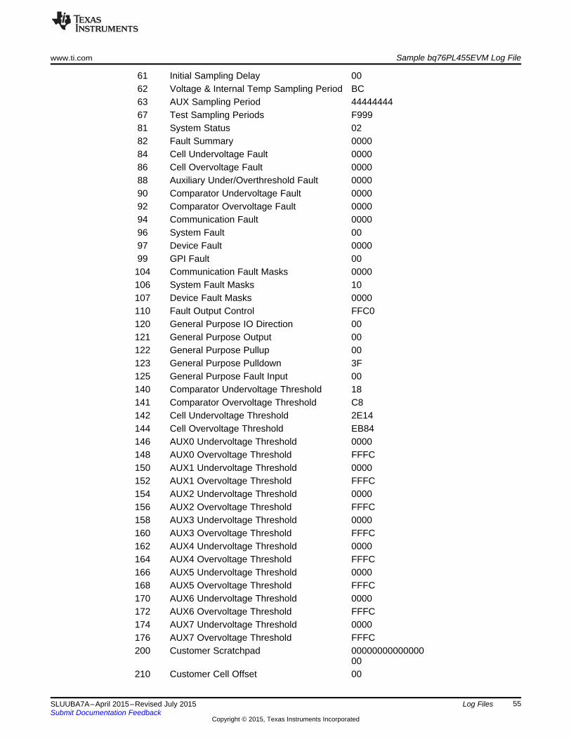
www.ti.com Sample bq76PL455EVM Log File
61 Initial Sampling Delay 0062 Voltage & Internal Temp Sampling Period BC63 AUX Sampling Period 4444444467 Test Sampling Periods F99981 System Status 0282 Fault Summary 000084 Cell Undervoltage Fault 000086 Cell Overvoltage Fault 000088 Auxiliary Under/Overthreshold Fault 000090 Comparator Undervoltage Fault 000092 Comparator Overvoltage Fault 000094 Communication Fault 000096 System Fault 0097 Device Fault 000099 GPI Fault 00
104 Communication Fault Masks 0000106 System Fault Masks 10107 Device Fault Masks 0000110 Fault Output Control FFC0120 General Purpose IO Direction 00121 General Purpose Output 00122 General Purpose Pullup 00123 General Purpose Pulldown 3F125 General Purpose Fault Input 00140 Comparator Undervoltage Threshold 18141 Comparator Overvoltage Threshold C8142 Cell Undervoltage Threshold 2E14144 Cell Overvoltage Threshold EB84146 AUX0 Undervoltage Threshold 0000148 AUX0 Overvoltage Threshold FFFC150 AUX1 Undervoltage Threshold 0000152 AUX1 Overvoltage Threshold FFFC154 AUX2 Undervoltage Threshold 0000156 AUX2 Overvoltage Threshold FFFC158 AUX3 Undervoltage Threshold 0000160 AUX3 Overvoltage Threshold FFFC162 AUX4 Undervoltage Threshold 0000164 AUX4 Overvoltage Threshold FFFC166 AUX5 Undervoltage Threshold 0000168 AUX5 Overvoltage Threshold FFFC170 AUX6 Undervoltage Threshold 0000172 AUX6 Overvoltage Threshold FFFC174 AUX7 Undervoltage Threshold 0000176 AUX7 Overvoltage Threshold FFFC200 Customer Scratchpad 00000000000000
00210 Customer Cell Offset 00
55SLUUBA7A–April 2015–Revised July 2015 Log FilesSubmit Documentation Feedback
Copyright © 2015, Texas Instruments Incorporated
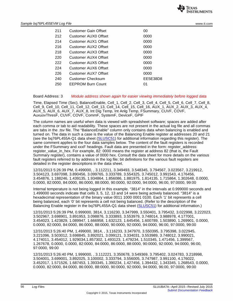
Sample bq76PL455EVM Log File www.ti.com
211 Customer Gain Offset 00212 Customer AUX0 Offset 0000214 Customer AUX1 Offset 0000216 Customer AUX2 Offset 0000218 Customer AUX3 Offset 0000220 Customer AUX4 Offset 0000222 Customer AUX5 Offset 0000224 Customer AUX6 Offset 0000226 Customer AUX7 Offset 0000240 Customer Checksum EE5E38D8250 EEPROM Burn Count 01
Board Address: 3 Module address shown again for easier viewing immediately before logged data
Time, Elapsed Time (Sec), BalanceEnable, Cell_1, Cell_2, Cell_3, Cell_4, Cell_5, Cell_6, Cell_7, Cell_8,Cell_9, Cell_10, Cell_11, Cell_12, Cell_13, Cell_14, Cell_15, Cell_16, AUX_1, AUX_2, AUX_3, AUX_4,AUX_5, AUX_6, AUX_7, AUX_8, Int Dig Temp, Int Anlg Temp, FSummary, CUVF, COVF,AuxuovThresF, CUVF, COVF, CommF, SystemF, DeviceF, GPIF
The column names are useful when data is viewed with spreadsheet software; spaces are added aftereach comma or tab to aid readability. These spaces are not present in the actual log file and all commasare tabs in the .tsv file. The “BalanceEnable” column only contains data when balancing is enabled andturned on. The data in such a case is the value of the Balancing Enable register at addresses 20 and 21(see the bq76PL455A-Q1 data sheet (SLUSC51) for additional information regarding this register). Thesame comment applies to the four data samples below. The content of the fault registers is recordedunder the FSummary and xxxF headings. Fault data are presented in the form: register_address:register_value_in_hex. For example, 82: 0000 means the register at address 82 (that is, the FaultSummary register), contains a value of 0000 hex. Consult the data sheet for more details on the variousfault registers referred to by address in the log file; bit definitions for the various fault regsiters aredetailed in the register descriptions in the data sheet.
12/31/2013 5:26:39 PM, 0.499000, , 3.112211, 3.349493, 3.548345, 3.794567, 3.023567, 3.219912,3.504123, 3.697098, 3.890456, 3.099765, 3.333789, 3.554325, 3.745012, 3.991543, 4.176456,3.454876, 1.188246, 1.439135, 1.934864, 1.856086, 1.881975, 1.814135, 1.715864, 1.302648, 0.0000,0.0000, 82:0000, 84:0000, 86:0000, 88:0000, 90:0000, 92:0000, 94:0000, 96:00, 97:0000, 99:00
Internal temperature is not being logged in this example. “3814” in the intervals at 0.999000 seconds and1.499000 seconds indicate that cells 3, 5, 12, 13 and 14 were being actively balanced. “3814” is ahexadecimal representation of the binary value 0011 1000 0001 0100. Each ‘1’ bit represents a cellbeing balanced, each ‘0’ bit represents a cell not being balanced. (Refer to the description of theBalancing Enable register in the bq76PL455A-Q1 data sheet (SLUSC51) for additional information.)
12/31/2013 5:26:39 PM, 0.999000, 3814, 3.116230, 3.347999, 3.550401, 3.795432, 3.022998, 3.222023,3.502967, 3.698901, 3.891953, 3.098876, 3.333893, 3.553979, 3.748014, 3.988978, 4.177001,3.454023, 1.423829, 1.089947, 1.666958, 1.632123, 1.645456, 1.600789, 1.503890, 1.269901, 0.0000,0.0000, 82:0000, 84:0000, 86:0000, 88:0000, 90:0000, 92:0000, 94:0000, 96:00, 97:0000, 99:00
12/31/2013 5:26:40 PM, 1.499000, 3814, , 3.116233, 3.347970, 3.550395, 3.795398, 3.022945,3.221096, 3.503012, 3.698845, 3.892021, 3.099121, 3.334031, 3.553989, 3.748012, 3.990021,4.174011, 3.454012, 1.929034,1.857302, 1.493123, 1.479234, 1.510345, 1.471456, 1.399567,1.267678, 0.0000, 0.0000, 82:0000, 84:0000, 86:0000, 88:0000, 90:0000, 92:0000, 94:0000, 96:00,97:0000, 99:00
12/31/2013 5:26:40 PM, 1.999000, , 3.112221, 3.350678, 3.549369, 3.795402, 3.024783, 3.218998,3.504001, 3.699001, 3.892025, 3.100002, 3.333794, 3.556005, 3.747987, 3.991100, 4.176022,3.452017, 1.571526, 1.687453, 1.393345, 1.390234, 1.427456, 1.394432, 1.343345, 1.268543, 0.0000,0.0000, 82:0000, 84:0000, 86:0000, 88:0000, 90:0000, 92:0000, 94:0000, 96:00, 97:0000, 99:00
56 Log Files SLUUBA7A–April 2015–Revised July 2015Submit Documentation Feedback
Copyright © 2015, Texas Instruments Incorporated
www.ti.com Sample bq76PL455EVM Log File
NOTE: When logging data for all the bq76PL455EVMs, the specified target file name for thecollected data is appended with an underscore and the bq76PL455EVM address of theevaluation module from which the data were collected.
NOTE: From time to time, log file formats and other GUI features are adjusted slightly to add newfeatures. Although every effort is made to update this document appropriately when suchchanges are made, there may be some mismatch between this document and the version ofGUI being used.
57SLUUBA7A–April 2015–Revised July 2015 Log FilesSubmit Documentation Feedback
Copyright © 2015, Texas Instruments Incorporated
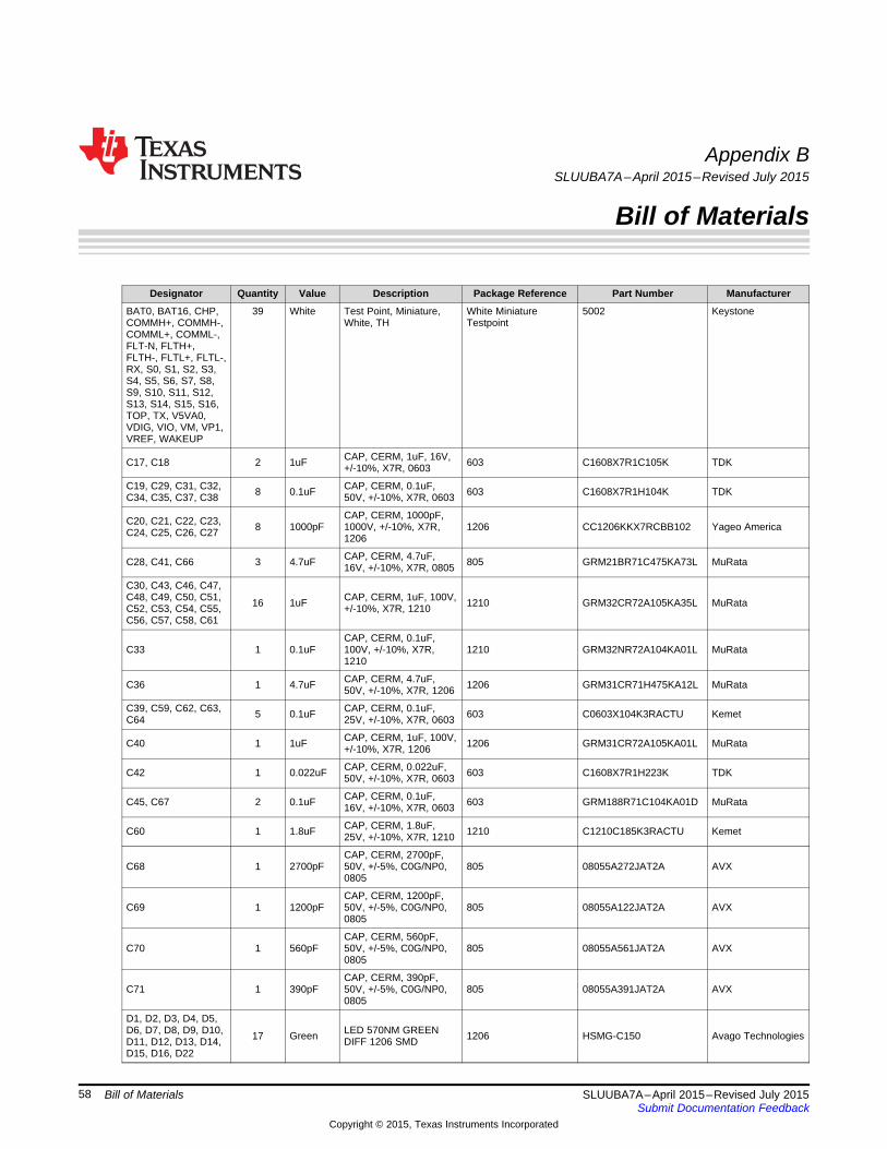
Appendix BSLUUBA7A–April 2015–Revised July 2015
Bill of Materials
Designator Quantity Value Description Package Reference Part Number Manufacturer
BAT0, BAT16, CHP, 39 White Test Point, Miniature, White Miniature 5002 KeystoneCOMMH+, COMMH-, White, TH TestpointCOMML+, COMML-,FLT-N, FLTH+,FLTH-, FLTL+, FLTL-,RX, S0, S1, S2, S3,S4, S5, S6, S7, S8,S9, S10, S11, S12,S13, S14, S15, S16,TOP, TX, V5VA0,VDIG, VIO, VM, VP1,VREF, WAKEUP
CAP, CERM, 1uF, 16V,C17, C18 2 1uF 603 C1608X7R1C105K TDK+/-10%, X7R, 0603
C19, C29, C31, C32, CAP, CERM, 0.1uF,8 0.1uF 603 C1608X7R1H104K TDKC34, C35, C37, C38 50V, +/-10%, X7R, 0603
CAP, CERM, 1000pF,C20, C21, C22, C23, 8 1000pF 1000V, +/-10%, X7R, 1206 CC1206KKX7RCBB102 Yageo AmericaC24, C25, C26, C27 1206
CAP, CERM, 4.7uF,C28, C41, C66 3 4.7uF 805 GRM21BR71C475KA73L MuRata16V, +/-10%, X7R, 0805
C30, C43, C46, C47,C48, C49, C50, C51, CAP, CERM, 1uF, 100V,16 1uF 1210 GRM32CR72A105KA35L MuRataC52, C53, C54, C55, +/-10%, X7R, 1210C56, C57, C58, C61
CAP, CERM, 0.1uF,C33 1 0.1uF 100V, +/-10%, X7R, 1210 GRM32NR72A104KA01L MuRata
1210
CAP, CERM, 4.7uF,C36 1 4.7uF 1206 GRM31CR71H475KA12L MuRata50V, +/-10%, X7R, 1206
C39, C59, C62, C63, CAP, CERM, 0.1uF,5 0.1uF 603 C0603X104K3RACTU KemetC64 25V, +/-10%, X7R, 0603
CAP, CERM, 1uF, 100V,C40 1 1uF 1206 GRM31CR72A105KA01L MuRata+/-10%, X7R, 1206
CAP, CERM, 0.022uF,C42 1 0.022uF 603 C1608X7R1H223K TDK50V, +/-10%, X7R, 0603
CAP, CERM, 0.1uF,C45, C67 2 0.1uF 603 GRM188R71C104KA01D MuRata16V, +/-10%, X7R, 0603
CAP, CERM, 1.8uF,C60 1 1.8uF 1210 C1210C185K3RACTU Kemet25V, +/-10%, X7R, 1210
CAP, CERM, 2700pF,C68 1 2700pF 50V, +/-5%, C0G/NP0, 805 08055A272JAT2A AVX
0805
CAP, CERM, 1200pF,C69 1 1200pF 50V, +/-5%, C0G/NP0, 805 08055A122JAT2A AVX
0805
CAP, CERM, 560pF,C70 1 560pF 50V, +/-5%, C0G/NP0, 805 08055A561JAT2A AVX
0805
CAP, CERM, 390pF,C71 1 390pF 50V, +/-5%, C0G/NP0, 805 08055A391JAT2A AVX
0805
D1, D2, D3, D4, D5,D6, D7, D8, D9, D10, LED 570NM GREEN17 Green 1206 HSMG-C150 Avago TechnologiesD11, D12, D13, D14, DIFF 1206 SMDD15, D16, D22
58 Bill of Materials SLUUBA7A–April 2015–Revised July 2015Submit Documentation Feedback
Copyright © 2015, Texas Instruments Incorporated
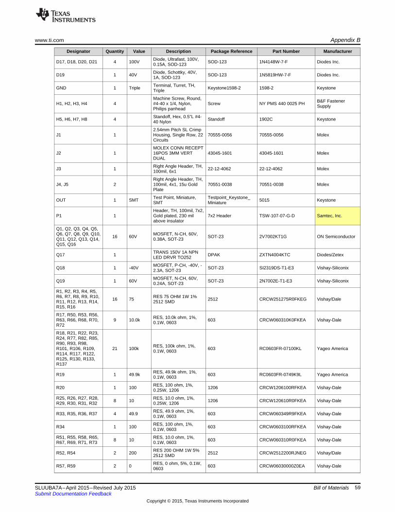
www.ti.com Appendix B
Designator Quantity Value Description Package Reference Part Number Manufacturer
Diode, Ultrafast, 100V,D17, D18, D20, D21 4 100V SOD-123 1N4148W-7-F Diodes Inc.0.15A, SOD-123
Diode, Schottky, 40V,D19 1 40V SOD-123 1N5819HW-7-F Diodes Inc.1A, SOD-123
Terminal, Turret, TH,GND 1 Triple Keystone1598-2 1598-2 KeystoneTriple
Machine Screw, Round, B&F FastenerH1, H2, H3, H4 4 #4-40 x 1/4, Nylon, Screw NY PMS 440 0025 PH SupplyPhilips panhead
Standoff, Hex, 0.5"L #4-H5, H6, H7, H8 4 Standoff 1902C Keystone40 Nylon
2.54mm Pitch SL CrimpJ1 1 Housing, Single Row, 22 70555-0056 70555-0056 Molex
Circuits
MOLEX CONN RECEPTJ2 1 16POS 3MM VERT 43045-1601 43045-1601 Molex
DUAL
Right Angle Header, TH,J3 1 22-12-4062 22-12-4062 Molex100mil, 6x1
Right Angle Header, TH,J4, J5 2 100mil, 4x1, 15u Gold 70551-0038 70551-0038 Molex
Plate
Test Point, Miniature, Testpoint_Keystone_OUT 1 SMT 5015 KeystoneSMT Miniature
Header, TH, 100mil, 7x2,P1 1 Gold plated, 230 mil 7x2 Header TSW-107-07-G-D Samtec, Inc.
above insulator
Q1, Q2, Q3, Q4, Q5,Q6, Q7, Q8, Q9, Q10, MOSFET, N-CH, 60V,16 60V SOT-23 2V7002KT1G ON SemiconductorQ11, Q12, Q13, Q14, 0.38A, SOT-23Q15, Q16
TRANS 150V 1A NPNQ17 1 DPAK ZXTN4004KTC Diodes/ZetexLED DRVR TO252
MOSFET, P-CH, -40V, -Q18 1 -40V SOT-23 SI2319DS-T1-E3 Vishay-Siliconix2.3A, SOT-23
MOSFET, N-CH, 60V,Q19 1 60V SOT-23 2N7002E-T1-E3 Vishay-Siliconix0.24A, SOT-23
R1, R2, R3, R4, R5,R6, R7, R8, R9, R10, RES 75 OHM 1W 1%16 75 2512 CRCW251275R0FKEG Vishay/DaleR11, R12, R13, R14, 2512 SMDR15, R16
R17, R50, R53, R56, RES, 10.0k ohm, 1%,R63, R66, R68, R70, 9 10.0k 603 CRCW060310K0FKEA Vishay-Dale0.1W, 0603R72
R18, R21, R22, R23,R24, R77, R82, R85,R90, R93, R98, RES, 100k ohm, 1%,R101, R106, R109, 21 100k 603 RC0603FR-07100KL Yageo America0.1W, 0603R114, R117, R122,R125, R130, R133,R137
RES, 49.9k ohm, 1%,R19 1 49.9k 603 RC0603FR-0749K9L Yageo America0.1W, 0603
RES, 100 ohm, 1%,R20 1 100 1206 CRCW1206100RFKEA Vishay-Dale0.25W, 1206
R25, R26, R27, R28, RES, 10.0 ohm, 1%,8 10 1206 CRCW120610R0FKEA Vishay-DaleR29, R30, R31, R32 0.25W, 1206
RES, 49.9 ohm, 1%,R33, R35, R36, R37 4 49.9 603 CRCW060349R9FKEA Vishay-Dale0.1W, 0603
RES, 100 ohm, 1%,R34 1 100 603 CRCW0603100RFKEA Vishay-Dale0.1W, 0603
R51, R55, R58, R65, RES, 10.0 ohm, 1%,8 10 603 CRCW060310R0FKEA Vishay-DaleR67, R69, R71, R73 0.1W, 0603
RES 200 OHM 1W 5%R52, R54 2 200 2512 CRCW2512200RJNEG Vishay/Dale2512 SMD
RES, 0 ohm, 5%, 0.1W,R57, R59 2 0 603 CRCW06030000Z0EA Vishay-Dale0603
59SLUUBA7A–April 2015–Revised July 2015 Bill of MaterialsSubmit Documentation Feedback
Copyright © 2015, Texas Instruments Incorporated
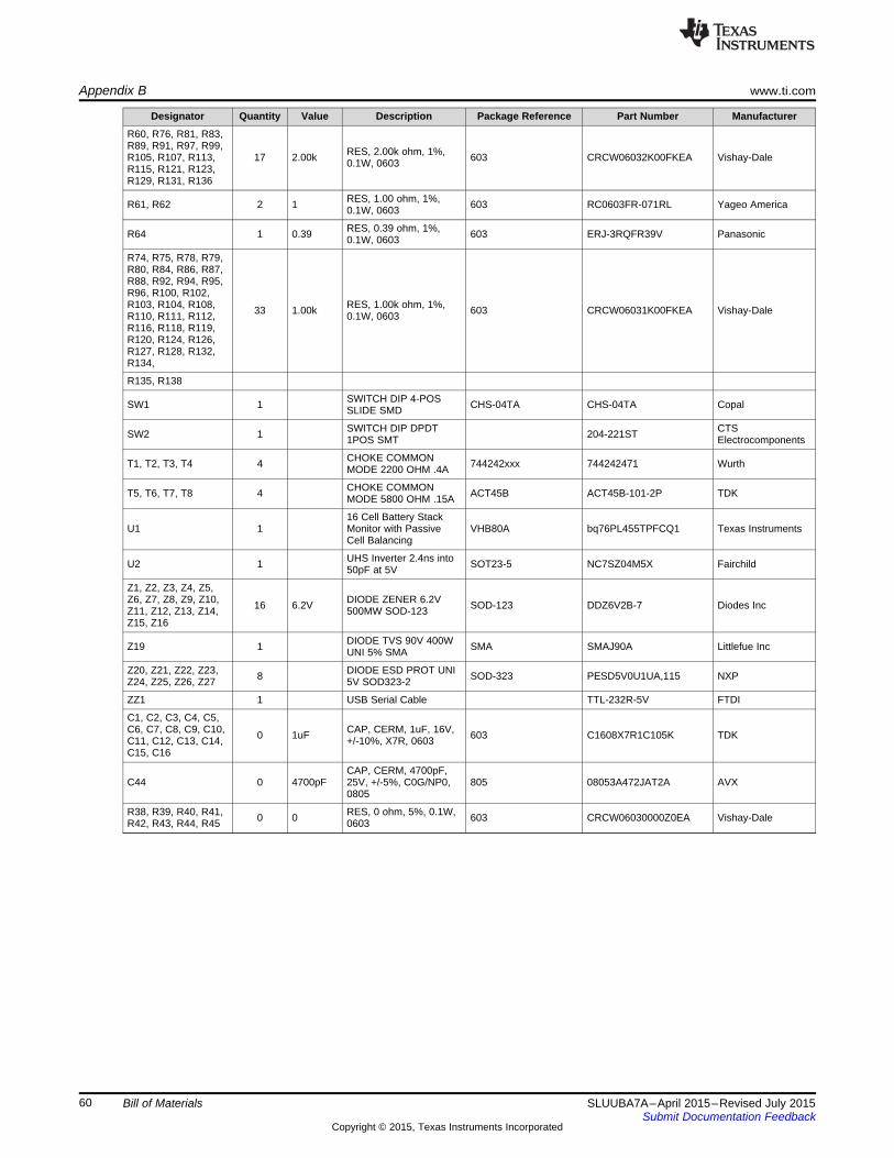
Appendix B www.ti.com
Designator Quantity Value Description Package Reference Part Number Manufacturer
R60, R76, R81, R83,R89, R91, R97, R99, RES, 2.00k ohm, 1%,R105, R107, R113, 17 2.00k 603 CRCW06032K00FKEA Vishay-Dale0.1W, 0603R115, R121, R123,R129, R131, R136
RES, 1.00 ohm, 1%,R61, R62 2 1 603 RC0603FR-071RL Yageo America0.1W, 0603
RES, 0.39 ohm, 1%,R64 1 0.39 603 ERJ-3RQFR39V Panasonic0.1W, 0603
R74, R75, R78, R79,R80, R84, R86, R87,R88, R92, R94, R95,R96, R100, R102,R103, R104, R108, RES, 1.00k ohm, 1%,33 1.00k 603 CRCW06031K00FKEA Vishay-DaleR110, R111, R112, 0.1W, 0603R116, R118, R119,R120, R124, R126,R127, R128, R132,R134,
R135, R138
SWITCH DIP 4-POSSW1 1 CHS-04TA CHS-04TA CopalSLIDE SMD
SWITCH DIP DPDT CTSSW2 1 204-221ST1POS SMT Electrocomponents
CHOKE COMMONT1, T2, T3, T4 4 744242xxx 744242471 WurthMODE 2200 OHM .4A
CHOKE COMMONT5, T6, T7, T8 4 ACT45B ACT45B-101-2P TDKMODE 5800 OHM .15A
16 Cell Battery StackU1 1 Monitor with Passive VHB80A bq76PL455TPFCQ1 Texas Instruments
Cell Balancing
UHS Inverter 2.4ns intoU2 1 SOT23-5 NC7SZ04M5X Fairchild50pF at 5V
Z1, Z2, Z3, Z4, Z5,Z6, Z7, Z8, Z9, Z10, DIODE ZENER 6.2V16 6.2V SOD-123 DDZ6V2B-7 Diodes IncZ11, Z12, Z13, Z14, 500MW SOD-123Z15, Z16
DIODE TVS 90V 400WZ19 1 SMA SMAJ90A Littlefue IncUNI 5% SMA
Z20, Z21, Z22, Z23, DIODE ESD PROT UNI8 SOD-323 PESD5V0U1UA,115 NXPZ24, Z25, Z26, Z27 5V SOD323-2
ZZ1 1 USB Serial Cable TTL-232R-5V FTDI
C1, C2, C3, C4, C5,C6, C7, C8, C9, C10, CAP, CERM, 1uF, 16V,0 1uF 603 C1608X7R1C105K TDKC11, C12, C13, C14, +/-10%, X7R, 0603C15, C16
CAP, CERM, 4700pF,C44 0 4700pF 25V, +/-5%, C0G/NP0, 805 08053A472JAT2A AVX
0805
R38, R39, R40, R41, RES, 0 ohm, 5%, 0.1W,0 0 603 CRCW06030000Z0EA Vishay-DaleR42, R43, R44, R45 0603
60 Bill of Materials SLUUBA7A–April 2015–Revised July 2015Submit Documentation Feedback
Copyright © 2015, Texas Instruments Incorporated
Appendix CSLUUBA7A–April 2015–Revised July 2015
Schematics
61SLUUBA7A–April 2015–Revised July 2015 SchematicsSubmit Documentation Feedback
Copyright © 2015, Texas Instruments Incorporated
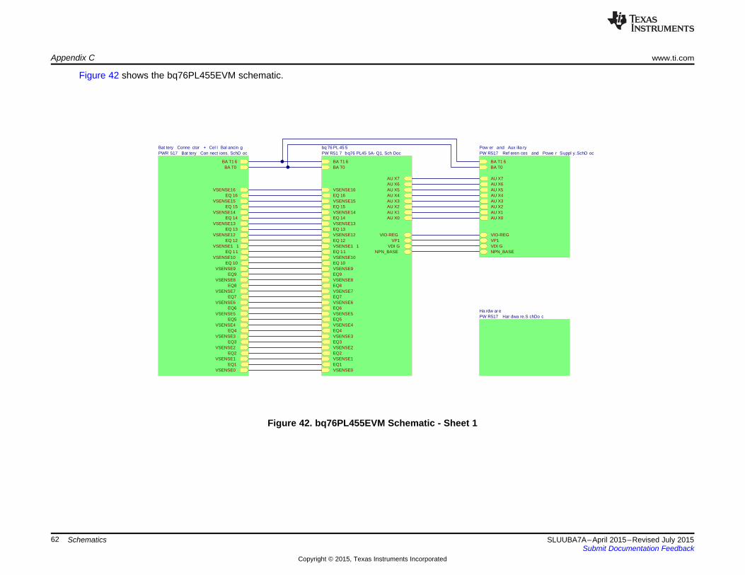
BA T0BA T1 6
EQ1
EQ 14
EQ 15
EQ 16
VSENSE0
VSENSE1
VSENSE2
VSENSE3
VSENSE4
VSENSE5
VSENSE6
VSENSE7
VSENSE8
VSENSE9
VSENSE10
VSENSE1 1
VSENSE12
VSENSE13
VSENSE14
VSENSE15
VSENSE16
EQ2
EQ3
EQ4
EQ5
EQ6
EQ7
EQ8
EQ9
EQ 10
EQ 11
EQ 12
EQ 13
AU X1AU X2AU X3
NPN_BASEVDI G
VP1
AU X0
VIO-REG
AU X4AU X5AU X6AU X7
bq 76 PL 45 5PW R51 7 bq76 PL45 5A- Q1. Sch Doc
Ha rdw ar ePW R517 Har dwa re.S chDo c
VSENSE16
VSENSE15
VSENSE14
VSENSE13
VSENSE12
VSENSE1 1
VSENSE10
VSENSE9
VSENSE8
VSENSE7
VSENSE6
VSENSE5
VSENSE4
VSENSE3
VSENSE2
VSENSE1
VSENSE0
EQ 16
EQ 15
EQ 14
EQ 13
EQ 12
EQ 11
EQ 10
EQ9
EQ8
EQ7
EQ6
EQ5
EQ4
EQ3
EQ2
EQ1
BA T1 6BA T0
Bat tery Conne ctor + Cel l Bal ancin gPWR 517 Bat tery Con nect ions. SchD oc
VDI GVP1
AU X1
NPN_BASE
BA T1 6
AU X3AU X2
AU X0
VIO-REG
AU X4AU X5AU X6AU X7
BA T0
Pow er and Aux ilia ryPW R517 Ref eren ces and Powe r Suppl y.SchD oc
Appendix C www.ti.com
Figure 42 shows the bq76PL455EVM schematic.
Figure 42. bq76PL455EVM Schematic - Sheet 1
62 Schematics SLUUBA7A–April 2015–Revised July 2015Submit Documentation Feedback
Copyright © 2015, Texas Instruments Incorporated
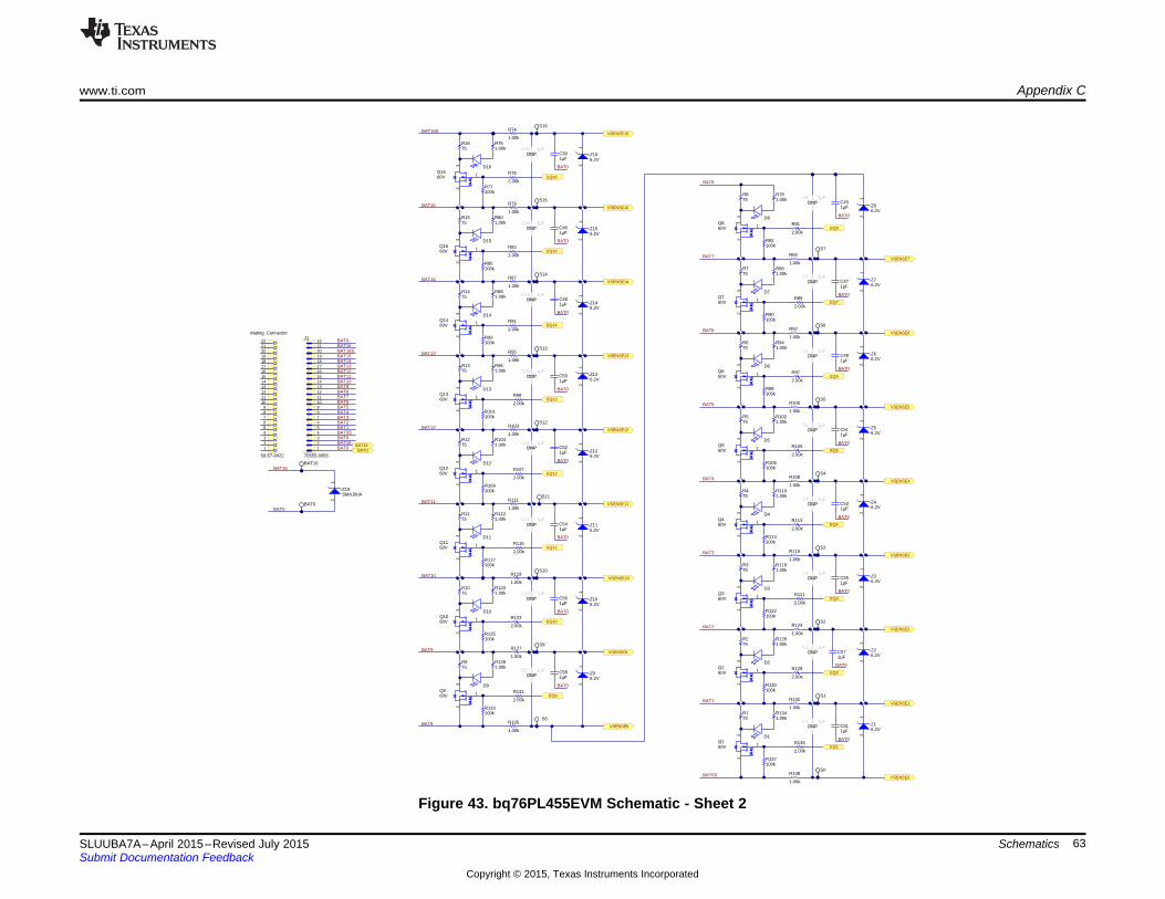
EQ7
EQ6
EQ10
EQ9
EQ11
EQ14
VSENSE15
EQ15
EQ16
EQ5
VSENSE3
EQ4
EQ3
VSENSE1
VSENSE0
VSENSE2
EQ1
EQ2
100kR137
BAT1
100kR130
100kR114
100kR122
1.00k
R138
BAT2
100kR106
100kR98
100kR90
100kR133
100kR125
100kR117
100kR77
1.00kR75
D16
1.00kR80
D15
1.00kR88
D14
D13
1.00kR104
D12
1.00kR112
D11
1.00kR120
D10
1.00kR128
D9
1.00kR86
D7
1.00kR94
D6
1.00kR102
D5
1.00kR110
D4
1.00kR118
D3
1.00kR126
D2
1.00kR134
D1
S0
S1
S2
S3
S10
S11
S14
S15
BAT16S
1.00k
R79
1.00k
R74S16
VSENSE16
100kR85
1.00k
R87VSENSE14
100kR93
VSENSE13
S13
1.00k
R95
1.00kR96
EQ13
100kR101
VSENSE12
S12
1.00k
R103
EQ12
100kR109
1.00k
R111VSENSE11
1.00k
R119VSENSE10
1.00k
R127VSENSE9
S9
1.00k
R135VSENSE8
S8
EQ8
100kR82
1.00kR78
D8
VSENSE7
S7
1.00k
R84
VSENSE6
S6
1.00k
R92
1.00k
R100VSENSE5
S5
BAT15
BAT5
BAT6
BAT7
BAT8
1.00k
R108VSENSE4
S4BAT4
1.00k
R116BAT3
1.00k
R124
1.00k
R132
BAT0S
BAT8
BAT14
BAT13
BAT12
BAT11
BAT10
BAT9
123456789
10111213141516171819202122
50-57-9422
BAT16
BAT0
BAT16BAT0
BAT9BAT8BAT7
BAT4BAT5BAT6
BAT10BAT11
BAT3BAT2BAT1BAT0SBAT0BAT16BAT0
BAT0
BAT12BAT13BAT14BAT15BAT16SBAT16
12345678910111213141516171819202122
J1
70555-0056
2.00k
R76
2.00k
R83
2.00k
R91
2.00k
R99
2.00k
R107
2.00k
R115
2.00k
R123
2.00k
R131
2.00k
R81
2.00k
R89
2.00k
R97
2.00k
R105
2.00k
R113
2.00k
R129
2.00k
R121
2.00k
R136
75R16
75R15
75R14
75R13
75R12
75R11
75R10
75R9
75R1
75R2
75R3
75R4
75R5
75R6
75R7
75R8
12
Z19SMAJ90A
BAT0
BAT16
1µFC16DNP
1µFC15DNP
1µFC14DNP
1µFC13DNP
1µFC12DNP
1µFC11DNP
1µFC10DNP
1µFC9DNP
1µFC8DNP
1µFC7DNP
1µFC6DNP
1µFC5DNP
1µFC4DNP
1µFC3DNP
1µFC2DNP
1µFC1DNP
60V 1
23
Q16
60V 1
23
Q15
60V 1
23
Q14
60V 1
23
Q13
60V 1
23
Q12
60V 1
23
Q11
60V 1
23
Q10
60V 1
23
Q9
60V 1
23
Q8
60V 1
23
Q7
60V 1
23
Q6
60V 1
23
Q5
60V 1
23
Q4
60V 1
23
Q3
60V 1
23
Q2
60V 1
23
Q1
1µFC58
BAT0
1µFC47
BAT0
1µFC61
BAT0
1µFC57
BAT0
1µFC55
BAT0
1µFC53
BAT0
1µFC51
BAT0
1µFC49
BAT0
1µFC43
BAT0
1µFC56
BAT0
1µFC54
BAT0
1µFC52
BAT0
1µFC50
BAT0
1µFC48
BAT0
1µFC46
BAT0
1µFC30
BAT0
Mating Connector
6.2V
12
Z9
6.2V
12
Z10
6.2V
12
Z11
6.2V
12
Z12
6.2V
12
Z14
6.2V
12
Z15
6.2V
12
Z16
6.2V
12
Z13
6.2V
12
Z1
6.2V
12
Z2
6.2V
12
Z3
6.2V
12
Z4
6.2V
12
Z5
6.2V
12
Z6
6.2V
12
Z7
6.2V
12
Z8
www.ti.com Appendix C
Figure 43. bq76PL455EVM Schematic - Sheet 2
63SLUUBA7A–April 2015–Revised July 2015 SchematicsSubmit Documentation Feedback
Copyright © 2015, Texas Instruments Incorporated
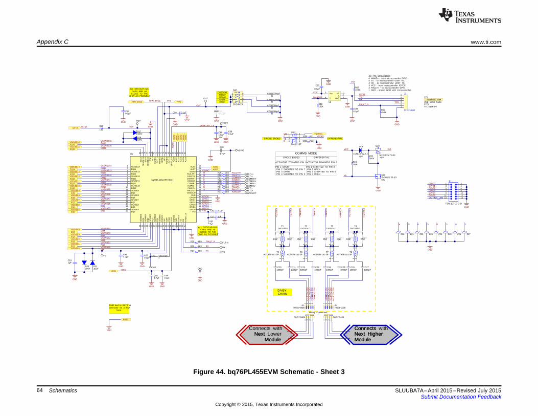
Connects with
EQ15 EQ15VSENSE15
ALL DECOUPLING CAPS ARE AS
CLOSE TO THE CHIP AS POSSIBLE
GND
390pF560pF
1200pF2700pF
CUSTOM
100
R20BAT16 BAT16
AU
X1
GPIO1GPIO0
GPIO2
ALL DECOUPLING CAPS ARE AS
CLOSE TO THE CHIP AS POSSIBLE
AU
X2
AU
X3
0.1µFC62
VDIG
GND
VM
VSENSE4
VSENSE3
VSENSE2
VSENSE1
VSENSE0
EQ4
EQ3
EQ2
EQ1
EQ4VSENSE4
EQ3VSENSE3
EQ2VSENSE2
EQ1VSENSE0
VSENSE1
GND
0.1µFC63
0.1µFC64
VSENSE7
VSENSE6
VSENSE5
EQ7
EQ6
EQ5
VSENSE10
VSENSE9
VSENSE8
EQ10
EQ9
EQ8
VSENSE11EQ11
VSENSE12EQ12
VSENSE13EQ13
VSENSE14EQ14
EQ13
EQ12VSENSE12
EQ11VSENSE11
EQ10VSENSE10
EQ9VSENSE9
EQ8VSENSE8
EQ7VSENSE7
EQ6VSENSE6
EQ5VSENSE5
VM
GND
VREF_INT_2.5VREF
NPN_BASE VP1
FAULT_N
RX
TX
FAULTL-FAULTL+
FLT-N
RX
TX
4.7µFC66
0.022µFC42
GND
NC 1
A 2
GND 3Y4
Vcc5
U2
GND
0.1µF
C67
GND
WAKE
VSENSE15
VSENSE16EQ16
VSENSE16EQ16
0.1µFC59
0.1µFC39
GND GND
GND
GND
TOP
VCC
VCC
10.0R32
GND
VIO
GPIO0GPIO1GPIO2GPIO3GPIO4GPIO5
10.0R31
10.0R28
10.0R3010.0R29
10.0R2710.0R2610.0R25
COMMH+COMMH-
FAULTH-FAULTH+
COMML+COMML-
WAKEUP GPIO3GPIO4GPIO5
GND
DAISY CHAIN
1000pFC27
ISO
-FA
ULT
H+
1000pFC26
ISO
-FA
ULT
H-
1000pFC25
1000pFC24
1000pFC23
ISO
-FA
ULT
L-
1000pFC21
ISO
-CO
MM
L-
1000pFC20
ISO
-CO
MM
L+
1000pFC22
ISO
-FA
ULT
L+
ISO
-CO
MM
H-
ISO
-CO
MM
H+
WAKEUP
0.1µFC33
CHP
4.7µFC41
A B C D E F
Z20 Z21 Z22 Z23 Z24 Z25 Z26 Z27
G H
DIFFERENTIALSINGLE ENDED
COMMS MODEDIFFERENTIALSINGLE ENDED
ACTUATOR TOWARDS PIN 1ACTUATOR TOWARDS PIN 8
PIN 1 OPEN PIN 2 SHORTED TO PIN 7 PIN 3 OPEN PIN 4 SHORTED TO PIN 5
PIN 1 SHORTED TO PIN 8 PIN 2 OPEN PIN 3 SHORTED TO PIN 6 PIN 4 OPEN
ABCDEFGH
Connects with Next Higher Module
Connects Next Higher Module
Next Lower Module
Next Module
123456
J3
22-12-4062
100VD18
100VD17
AU
X0
WAKEUP
AU
X0
GND
1234
J570551-0038
1234
50-57-9404
1234
50-57-9404
49.9R37
49.9R36
49.9R35
49.9R33
GND
VDIG
V5VAO
OUT
OUT TX
FAULT_N
1234
8765
ONSW1
CHS-04TA
4.7µF
C28
V5VA0
100R34VIO
GND
49.9kR19
RX
10.0kR17
VIO
-40V
Q18
SI2319DS-T1-E3
60V
Q192N7002E-T1-E3
100kR23
GND
VIOVCC
C
D
V5VAOVg
VIO100k R21
100k R22
100kR24
VIO
VIO-REG
1µFC17
40V
D19
1N5819HW-7-F
100kR18
GND
AUX7
AU
X5
AUX6
AU
X4
0.1µFC45
GND
1µFC18
25V1.8µFC60
4700pFC44DNP 390pFC71
560pFC70
2700pFC68
1200pFC69
100VD21
100VD20
FLTL+FLTL-COMML+COMML-COMMH-COMMH+FLTH-FLTH+
VSENSE13EQ14VSENSE14
TOP
Vg
Mating Connectors1234
J470551-0038
1 82 73 64 5
SW2
204-221ST
6 WAKEn - from microcontroller GPIOJ3 Pin Description
5 TX - to microcontroller UART RX4 RX - to microcontroller UART TX3 VCC - from microcontroller IOVCC2 FAULTn - to microcontroller GPIO1 GND - shared GND with microcontroller
Assembly Note
TTL-232R-5VFTDI
ZZ1
USB Serial Cable
GND
GND
GND
GND
GND
NPN_BASE VP1
GNDGND
1 23 45 67 89 10
11 1213 14
P1
TSW-107-07-G-D
GND
GND tied to BAT0 at connector via a thick
trace.
BAT0
GND
GND
CO
MM
H-
CO
MM
H+
FA
ULT
H-
FA
ULT
H+
FA
ULT
L-
FA
ULT
L+
CO
MM
L-
CO
MM
L+
1 234
T1744242471
1 234
T5ACT45B-101-2P
1 234
T2744242471
1 234
T6ACT45B-101-2P
1 234
T3744242471
1 234
T7ACT45B-101-2P
1 234
T4744242471
1 234
T8ACT45B-101-2P
0R39
DNP0R38
DNP 0R41
DNP0R40
DNP 0R43
DNP0R42
DNP 0R45
DNP0R44
DNP
SENSE117
SENSE141
EQ118
SENSE911
EQ520
SENSE813
EQ814
SENSE715
EQ716
SENSE617
EQ618
EQ142
SENSE519
SENSE133
EQ134
SENSE125
EQ126
EQ
324
EQ
422
SE
NS
E3
23
SE
NS
E4
21
SE
NS
E2
25
SENSE109
EQ1010
EQ912
SE
NS
E1
27E
Q2
26
TX
38
CH
M33
VM
31
CH
P32
DG
ND
130
VD
IG34
RX
39
NC
136
DG
ND
337
DG
ND
235
FA
ULT
_N40
COMMH- 54
AUX6 60
COMML- 53
FAULTL+ 50
VIO 41
GND 48
GPIO0 47
GPIO1 46
GPIO2 45
GPIO3 44
GPIO4 43
AUX7 59
GPIO5 42
V5VA0 58
FAULTH+ 57
FAULTH- 56
COMMH+ 55
COMML+ 52
FAULTL- 51
WAKEUP 49
SE
NS
E16
77
SE
NS
E15
79
EQ
1678
EQ
1580
TO
P76
AG
ND
272
AG
ND
174
OU
T_1
73
NC
275
NP
NB
71
VR
EF
_2.5
67
AG
ND
369
OU
T_2
68
VP
170
AU
X0
66
AU
X4
62
AU
X2
64
AU
X3
63
AU
X1
65
AU
X5
61
SE
NS
E0
29E
Q1
28U1
bq76PL455ATPFCRQ1
Appendix C www.ti.com
Figure 44. bq76PL455EVM Schematic - Sheet 3
64 Schematics SLUUBA7A–April 2015–Revised July 2015Submit Documentation Feedback
Copyright © 2015, Texas Instruments Incorporated
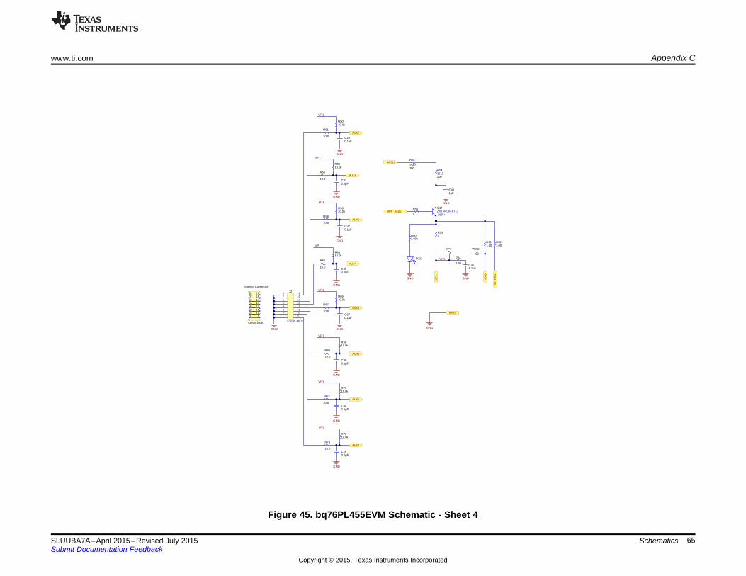
GND
10.0kR66
NPN_BASE
BAT16
0
R57
GND
10.0kR68
GND
10.0kR72
VP1
VP1
VP1
GND
10.0kR70
VP1
10.0
R69
10.0
R67
10.0
R71
10.0
R73
AUX3
AUX2
AUX1
AUX0
VP1
12345678
910111213141516
43025-1608
GND
12345678
910111213141516
J2
43045-1601
GND
10.0kR63
VP1
10.0
R65AUX4
GND
10.0kR56
VP1
10.0
R58AUX5
GND
10.0kR53
VP1
10.0
R55AUX6
GND
10.0kR50
VP1
10.0
R51AUX7
0.1µFC29
0.1µFC31
0.1µFC32
0.1µFC35
0.1µFC37
0.1µFC38
0.1µFC34
0.1µFC19
0.39
R64
Mating Connector
2512200
R52
2512200
R54
GND
1µFC40
150V
Q17ZXTN4004KTC
2.00kR60
D22
GND
0R59
VP
1
VP1
4.7µFC36
GND
1.00R61
VD
IG
VDIG1.00R62
VIO
-RE
G
GND
BAT0
www.ti.com Appendix C
Figure 45. bq76PL455EVM Schematic - Sheet 4
65SLUUBA7A–April 2015–Revised July 2015 SchematicsSubmit Documentation Feedback
Copyright © 2015, Texas Instruments Incorporated
Revision History www.ti.com
Revision History
Changes from Original (April 2015) to A Revision .......................................................................................................... Page
• Added appendix title..................................................................................................................... 53• Added Appendix B: Bill of Materials ................................................................................................... 58• Added Appendix C: Schematics ....................................................................................................... 61
66 Revision History SLUUBA7A–April 2015–Revised July 2015Submit Documentation Feedback
Copyright © 2015, Texas Instruments Incorporated
STANDARD TERMS AND CONDITIONS FOR EVALUATION MODULES1. Delivery: TI delivers TI evaluation boards, kits, or modules, including any accompanying demonstration software, components, or
documentation (collectively, an “EVM” or “EVMs”) to the User (“User”) in accordance with the terms and conditions set forth herein.Acceptance of the EVM is expressly subject to the following terms and conditions.1.1 EVMs are intended solely for product or software developers for use in a research and development setting to facilitate feasibility
evaluation, experimentation, or scientific analysis of TI semiconductors products. EVMs have no direct function and are notfinished products. EVMs shall not be directly or indirectly assembled as a part or subassembly in any finished product. Forclarification, any software or software tools provided with the EVM (“Software”) shall not be subject to the terms and conditionsset forth herein but rather shall be subject to the applicable terms and conditions that accompany such Software
1.2 EVMs are not intended for consumer or household use. EVMs may not be sold, sublicensed, leased, rented, loaned, assigned,or otherwise distributed for commercial purposes by Users, in whole or in part, or used in any finished product or productionsystem.
2 Limited Warranty and Related Remedies/Disclaimers:2.1 These terms and conditions do not apply to Software. The warranty, if any, for Software is covered in the applicable Software
License Agreement.2.2 TI warrants that the TI EVM will conform to TI's published specifications for ninety (90) days after the date TI delivers such EVM
to User. Notwithstanding the foregoing, TI shall not be liable for any defects that are caused by neglect, misuse or mistreatmentby an entity other than TI, including improper installation or testing, or for any EVMs that have been altered or modified in anyway by an entity other than TI. Moreover, TI shall not be liable for any defects that result from User's design, specifications orinstructions for such EVMs. Testing and other quality control techniques are used to the extent TI deems necessary or asmandated by government requirements. TI does not test all parameters of each EVM.
2.3 If any EVM fails to conform to the warranty set forth above, TI's sole liability shall be at its option to repair or replace such EVM,or credit User's account for such EVM. TI's liability under this warranty shall be limited to EVMs that are returned during thewarranty period to the address designated by TI and that are determined by TI not to conform to such warranty. If TI elects torepair or replace such EVM, TI shall have a reasonable time to repair such EVM or provide replacements. Repaired EVMs shallbe warranted for the remainder of the original warranty period. Replaced EVMs shall be warranted for a new full ninety (90) daywarranty period.
3 Regulatory Notices:3.1 United States
3.1.1 Notice applicable to EVMs not FCC-Approved:This kit is designed to allow product developers to evaluate electronic components, circuitry, or software associated with the kitto determine whether to incorporate such items in a finished product and software developers to write software applications foruse with the end product. This kit is not a finished product and when assembled may not be resold or otherwise marketed unlessall required FCC equipment authorizations are first obtained. Operation is subject to the condition that this product not causeharmful interference to licensed radio stations and that this product accept harmful interference. Unless the assembled kit isdesigned to operate under part 15, part 18 or part 95 of this chapter, the operator of the kit must operate under the authority ofan FCC license holder or must secure an experimental authorization under part 5 of this chapter.3.1.2 For EVMs annotated as FCC – FEDERAL COMMUNICATIONS COMMISSION Part 15 Compliant:
CAUTIONThis device complies with part 15 of the FCC Rules. Operation is subject to the following two conditions: (1) This device may notcause harmful interference, and (2) this device must accept any interference received, including interference that may causeundesired operation.Changes or modifications not expressly approved by the party responsible for compliance could void the user's authority tooperate the equipment.
FCC Interference Statement for Class A EVM devicesNOTE: This equipment has been tested and found to comply with the limits for a Class A digital device, pursuant to part 15 ofthe FCC Rules. These limits are designed to provide reasonable protection against harmful interference when the equipment isoperated in a commercial environment. This equipment generates, uses, and can radiate radio frequency energy and, if notinstalled and used in accordance with the instruction manual, may cause harmful interference to radio communications.Operation of this equipment in a residential area is likely to cause harmful interference in which case the user will be required tocorrect the interference at his own expense.
SPACER
SPACER
SPACER
SPACER
SPACER
SPACER
SPACER
SPACER

FCC Interference Statement for Class B EVM devicesNOTE: This equipment has been tested and found to comply with the limits for a Class B digital device, pursuant to part 15 ofthe FCC Rules. These limits are designed to provide reasonable protection against harmful interference in a residentialinstallation. This equipment generates, uses and can radiate radio frequency energy and, if not installed and used in accordancewith the instructions, may cause harmful interference to radio communications. However, there is no guarantee that interferencewill not occur in a particular installation. If this equipment does cause harmful interference to radio or television reception, whichcan be determined by turning the equipment off and on, the user is encouraged to try to correct the interference by one or moreof the following measures:
• Reorient or relocate the receiving antenna.• Increase the separation between the equipment and receiver.• Connect the equipment into an outlet on a circuit different from that to which the receiver is connected.• Consult the dealer or an experienced radio/TV technician for help.
3.2 Canada3.2.1 For EVMs issued with an Industry Canada Certificate of Conformance to RSS-210
Concerning EVMs Including Radio Transmitters:This device complies with Industry Canada license-exempt RSS standard(s). Operation is subject to the following two conditions:(1) this device may not cause interference, and (2) this device must accept any interference, including interference that maycause undesired operation of the device.
Concernant les EVMs avec appareils radio:Le présent appareil est conforme aux CNR d'Industrie Canada applicables aux appareils radio exempts de licence. L'exploitationest autorisée aux deux conditions suivantes: (1) l'appareil ne doit pas produire de brouillage, et (2) l'utilisateur de l'appareil doitaccepter tout brouillage radioélectrique subi, même si le brouillage est susceptible d'en compromettre le fonctionnement.
Concerning EVMs Including Detachable Antennas:Under Industry Canada regulations, this radio transmitter may only operate using an antenna of a type and maximum (or lesser)gain approved for the transmitter by Industry Canada. To reduce potential radio interference to other users, the antenna typeand its gain should be so chosen that the equivalent isotropically radiated power (e.i.r.p.) is not more than that necessary forsuccessful communication. This radio transmitter has been approved by Industry Canada to operate with the antenna typeslisted in the user guide with the maximum permissible gain and required antenna impedance for each antenna type indicated.Antenna types not included in this list, having a gain greater than the maximum gain indicated for that type, are strictly prohibitedfor use with this device.
Concernant les EVMs avec antennes détachablesConformément à la réglementation d'Industrie Canada, le présent émetteur radio peut fonctionner avec une antenne d'un type etd'un gain maximal (ou inférieur) approuvé pour l'émetteur par Industrie Canada. Dans le but de réduire les risques de brouillageradioélectrique à l'intention des autres utilisateurs, il faut choisir le type d'antenne et son gain de sorte que la puissance isotroperayonnée équivalente (p.i.r.e.) ne dépasse pas l'intensité nécessaire à l'établissement d'une communication satisfaisante. Leprésent émetteur radio a été approuvé par Industrie Canada pour fonctionner avec les types d'antenne énumérés dans lemanuel d’usage et ayant un gain admissible maximal et l'impédance requise pour chaque type d'antenne. Les types d'antennenon inclus dans cette liste, ou dont le gain est supérieur au gain maximal indiqué, sont strictement interdits pour l'exploitation del'émetteur
3.3 Japan3.3.1 Notice for EVMs delivered in Japan: Please see http://www.tij.co.jp/lsds/ti_ja/general/eStore/notice_01.page 日本国内に
輸入される評価用キット、ボードについては、次のところをご覧ください。http://www.tij.co.jp/lsds/ti_ja/general/eStore/notice_01.page
3.3.2 Notice for Users of EVMs Considered “Radio Frequency Products” in Japan: EVMs entering Japan may not be certifiedby TI as conforming to Technical Regulations of Radio Law of Japan.
If User uses EVMs in Japan, not certified to Technical Regulations of Radio Law of Japan, User is required by Radio Law ofJapan to follow the instructions below with respect to EVMs:1. Use EVMs in a shielded room or any other test facility as defined in the notification #173 issued by Ministry of Internal
Affairs and Communications on March 28, 2006, based on Sub-section 1.1 of Article 6 of the Ministry’s Rule forEnforcement of Radio Law of Japan,
2. Use EVMs only after User obtains the license of Test Radio Station as provided in Radio Law of Japan with respect toEVMs, or
3. Use of EVMs only after User obtains the Technical Regulations Conformity Certification as provided in Radio Law of Japanwith respect to EVMs. Also, do not transfer EVMs, unless User gives the same notice above to the transferee. Please notethat if User does not follow the instructions above, User will be subject to penalties of Radio Law of Japan.
SPACER
SPACER
SPACER
SPACER
SPACER
【無線電波を送信する製品の開発キットをお使いになる際の注意事項】 開発キットの中には技術基準適合証明を受けていないものがあります。 技術適合証明を受けていないもののご使用に際しては、電波法遵守のため、以下のいずれかの措置を取っていただく必要がありますのでご注意ください。1. 電波法施行規則第6条第1項第1号に基づく平成18年3月28日総務省告示第173号で定められた電波暗室等の試験設備でご使用
いただく。2. 実験局の免許を取得後ご使用いただく。3. 技術基準適合証明を取得後ご使用いただく。
なお、本製品は、上記の「ご使用にあたっての注意」を譲渡先、移転先に通知しない限り、譲渡、移転できないものとします。上記を遵守頂けない場合は、電波法の罰則が適用される可能性があることをご留意ください。 日本テキサス・イ
ンスツルメンツ株式会社東京都新宿区西新宿6丁目24番1号西新宿三井ビル
3.3.3 Notice for EVMs for Power Line Communication: Please see http://www.tij.co.jp/lsds/ti_ja/general/eStore/notice_02.page電力線搬送波通信についての開発キットをお使いになる際の注意事項については、次のところをご覧ください。http://www.tij.co.jp/lsds/ti_ja/general/eStore/notice_02.page
SPACER4 EVM Use Restrictions and Warnings:
4.1 EVMS ARE NOT FOR USE IN FUNCTIONAL SAFETY AND/OR SAFETY CRITICAL EVALUATIONS, INCLUDING BUT NOTLIMITED TO EVALUATIONS OF LIFE SUPPORT APPLICATIONS.
4.2 User must read and apply the user guide and other available documentation provided by TI regarding the EVM prior to handlingor using the EVM, including without limitation any warning or restriction notices. The notices contain important safety informationrelated to, for example, temperatures and voltages.
4.3 Safety-Related Warnings and Restrictions:4.3.1 User shall operate the EVM within TI’s recommended specifications and environmental considerations stated in the user
guide, other available documentation provided by TI, and any other applicable requirements and employ reasonable andcustomary safeguards. Exceeding the specified performance ratings and specifications (including but not limited to inputand output voltage, current, power, and environmental ranges) for the EVM may cause personal injury or death, orproperty damage. If there are questions concerning performance ratings and specifications, User should contact a TIfield representative prior to connecting interface electronics including input power and intended loads. Any loads appliedoutside of the specified output range may also result in unintended and/or inaccurate operation and/or possiblepermanent damage to the EVM and/or interface electronics. Please consult the EVM user guide prior to connecting anyload to the EVM output. If there is uncertainty as to the load specification, please contact a TI field representative.During normal operation, even with the inputs and outputs kept within the specified allowable ranges, some circuitcomponents may have elevated case temperatures. These components include but are not limited to linear regulators,switching transistors, pass transistors, current sense resistors, and heat sinks, which can be identified using theinformation in the associated documentation. When working with the EVM, please be aware that the EVM may becomevery warm.
4.3.2 EVMs are intended solely for use by technically qualified, professional electronics experts who are familiar with thedangers and application risks associated with handling electrical mechanical components, systems, and subsystems.User assumes all responsibility and liability for proper and safe handling and use of the EVM by User or its employees,affiliates, contractors or designees. User assumes all responsibility and liability to ensure that any interfaces (electronicand/or mechanical) between the EVM and any human body are designed with suitable isolation and means to safelylimit accessible leakage currents to minimize the risk of electrical shock hazard. User assumes all responsibility andliability for any improper or unsafe handling or use of the EVM by User or its employees, affiliates, contractors ordesignees.
4.4 User assumes all responsibility and liability to determine whether the EVM is subject to any applicable international, federal,state, or local laws and regulations related to User’s handling and use of the EVM and, if applicable, User assumes allresponsibility and liability for compliance in all respects with such laws and regulations. User assumes all responsibility andliability for proper disposal and recycling of the EVM consistent with all applicable international, federal, state, and localrequirements.
5. Accuracy of Information: To the extent TI provides information on the availability and function of EVMs, TI attempts to be as accurateas possible. However, TI does not warrant the accuracy of EVM descriptions, EVM availability or other information on its websites asaccurate, complete, reliable, current, or error-free.
SPACER
SPACER
SPACER
SPACER
SPACER
SPACER

SPACER6. Disclaimers:
6.1 EXCEPT AS SET FORTH ABOVE, EVMS AND ANY WRITTEN DESIGN MATERIALS PROVIDED WITH THE EVM (AND THEDESIGN OF THE EVM ITSELF) ARE PROVIDED "AS IS" AND "WITH ALL FAULTS." TI DISCLAIMS ALL OTHERWARRANTIES, EXPRESS OR IMPLIED, REGARDING SUCH ITEMS, INCLUDING BUT NOT LIMITED TO ANY IMPLIEDWARRANTIES OF MERCHANTABILITY OR FITNESS FOR A PARTICULAR PURPOSE OR NON-INFRINGEMENT OF ANYTHIRD PARTY PATENTS, COPYRIGHTS, TRADE SECRETS OR OTHER INTELLECTUAL PROPERTY RIGHTS.
6.2 EXCEPT FOR THE LIMITED RIGHT TO USE THE EVM SET FORTH HEREIN, NOTHING IN THESE TERMS ANDCONDITIONS SHALL BE CONSTRUED AS GRANTING OR CONFERRING ANY RIGHTS BY LICENSE, PATENT, OR ANYOTHER INDUSTRIAL OR INTELLECTUAL PROPERTY RIGHT OF TI, ITS SUPPLIERS/LICENSORS OR ANY OTHER THIRDPARTY, TO USE THE EVM IN ANY FINISHED END-USER OR READY-TO-USE FINAL PRODUCT, OR FOR ANYINVENTION, DISCOVERY OR IMPROVEMENT MADE, CONCEIVED OR ACQUIRED PRIOR TO OR AFTER DELIVERY OFTHE EVM.
7. USER'S INDEMNITY OBLIGATIONS AND REPRESENTATIONS. USER WILL DEFEND, INDEMNIFY AND HOLD TI, ITSLICENSORS AND THEIR REPRESENTATIVES HARMLESS FROM AND AGAINST ANY AND ALL CLAIMS, DAMAGES, LOSSES,EXPENSES, COSTS AND LIABILITIES (COLLECTIVELY, "CLAIMS") ARISING OUT OF OR IN CONNECTION WITH ANYHANDLING OR USE OF THE EVM THAT IS NOT IN ACCORDANCE WITH THESE TERMS AND CONDITIONS. THIS OBLIGATIONSHALL APPLY WHETHER CLAIMS ARISE UNDER STATUTE, REGULATION, OR THE LAW OF TORT, CONTRACT OR ANYOTHER LEGAL THEORY, AND EVEN IF THE EVM FAILS TO PERFORM AS DESCRIBED OR EXPECTED.
8. Limitations on Damages and Liability:8.1 General Limitations. IN NO EVENT SHALL TI BE LIABLE FOR ANY SPECIAL, COLLATERAL, INDIRECT, PUNITIVE,
INCIDENTAL, CONSEQUENTIAL, OR EXEMPLARY DAMAGES IN CONNECTION WITH OR ARISING OUT OF THESETERMS ANDCONDITIONS OR THE USE OF THE EVMS PROVIDED HEREUNDER, REGARDLESS OF WHETHER TI HASBEEN ADVISED OF THE POSSIBILITY OF SUCH DAMAGES. EXCLUDED DAMAGES INCLUDE, BUT ARE NOT LIMITEDTO, COST OF REMOVAL OR REINSTALLATION, ANCILLARY COSTS TO THE PROCUREMENT OF SUBSTITUTE GOODSOR SERVICES, RETESTING, OUTSIDE COMPUTER TIME, LABOR COSTS, LOSS OF GOODWILL, LOSS OF PROFITS,LOSS OF SAVINGS, LOSS OF USE, LOSS OF DATA, OR BUSINESS INTERRUPTION. NO CLAIM, SUIT OR ACTION SHALLBE BROUGHT AGAINST TI MORE THAN ONE YEAR AFTER THE RELATED CAUSE OF ACTION HAS OCCURRED.
8.2 Specific Limitations. IN NO EVENT SHALL TI'S AGGREGATE LIABILITY FROM ANY WARRANTY OR OTHER OBLIGATIONARISING OUT OF OR IN CONNECTION WITH THESE TERMS AND CONDITIONS, OR ANY USE OF ANY TI EVMPROVIDED HEREUNDER, EXCEED THE TOTAL AMOUNT PAID TO TI FOR THE PARTICULAR UNITS SOLD UNDERTHESE TERMS AND CONDITIONS WITH RESPECT TO WHICH LOSSES OR DAMAGES ARE CLAIMED. THE EXISTENCEOF MORE THAN ONE CLAIM AGAINST THE PARTICULAR UNITS SOLD TO USER UNDER THESE TERMS ANDCONDITIONS SHALL NOT ENLARGE OR EXTEND THIS LIMIT.
9. Return Policy. Except as otherwise provided, TI does not offer any refunds, returns, or exchanges. Furthermore, no return of EVM(s)will be accepted if the package has been opened and no return of the EVM(s) will be accepted if they are damaged or otherwise not ina resalable condition. If User feels it has been incorrectly charged for the EVM(s) it ordered or that delivery violates the applicableorder, User should contact TI. All refunds will be made in full within thirty (30) working days from the return of the components(s),excluding any postage or packaging costs.
10. Governing Law: These terms and conditions shall be governed by and interpreted in accordance with the laws of the State of Texas,without reference to conflict-of-laws principles. User agrees that non-exclusive jurisdiction for any dispute arising out of or relating tothese terms and conditions lies within courts located in the State of Texas and consents to venue in Dallas County, Texas.Notwithstanding the foregoing, any judgment may be enforced in any United States or foreign court, and TI may seek injunctive reliefin any United States or foreign court.
Mailing Address: Texas Instruments, Post Office Box 655303, Dallas, Texas 75265Copyright © 2015, Texas Instruments Incorporated
spacer

IMPORTANT NOTICE
Texas Instruments Incorporated and its subsidiaries (TI) reserve the right to make corrections, enhancements, improvements and otherchanges to its semiconductor products and services per JESD46, latest issue, and to discontinue any product or service per JESD48, latestissue. Buyers should obtain the latest relevant information before placing orders and should verify that such information is current andcomplete. All semiconductor products (also referred to herein as “components”) are sold subject to TI’s terms and conditions of salesupplied at the time of order acknowledgment.TI warrants performance of its components to the specifications applicable at the time of sale, in accordance with the warranty in TI’s termsand conditions of sale of semiconductor products. Testing and other quality control techniques are used to the extent TI deems necessaryto support this warranty. Except where mandated by applicable law, testing of all parameters of each component is not necessarilyperformed.TI assumes no liability for applications assistance or the design of Buyers’ products. Buyers are responsible for their products andapplications using TI components. To minimize the risks associated with Buyers’ products and applications, Buyers should provideadequate design and operating safeguards.TI does not warrant or represent that any license, either express or implied, is granted under any patent right, copyright, mask work right, orother intellectual property right relating to any combination, machine, or process in which TI components or services are used. Informationpublished by TI regarding third-party products or services does not constitute a license to use such products or services or a warranty orendorsement thereof. Use of such information may require a license from a third party under the patents or other intellectual property of thethird party, or a license from TI under the patents or other intellectual property of TI.Reproduction of significant portions of TI information in TI data books or data sheets is permissible only if reproduction is without alterationand is accompanied by all associated warranties, conditions, limitations, and notices. TI is not responsible or liable for such altereddocumentation. Information of third parties may be subject to additional restrictions.Resale of TI components or services with statements different from or beyond the parameters stated by TI for that component or servicevoids all express and any implied warranties for the associated TI component or service and is an unfair and deceptive business practice.TI is not responsible or liable for any such statements.Buyer acknowledges and agrees that it is solely responsible for compliance with all legal, regulatory and safety-related requirementsconcerning its products, and any use of TI components in its applications, notwithstanding any applications-related information or supportthat may be provided by TI. Buyer represents and agrees that it has all the necessary expertise to create and implement safeguards whichanticipate dangerous consequences of failures, monitor failures and their consequences, lessen the likelihood of failures that might causeharm and take appropriate remedial actions. Buyer will fully indemnify TI and its representatives against any damages arising out of the useof any TI components in safety-critical applications.In some cases, TI components may be promoted specifically to facilitate safety-related applications. With such components, TI’s goal is tohelp enable customers to design and create their own end-product solutions that meet applicable functional safety standards andrequirements. Nonetheless, such components are subject to these terms.No TI components are authorized for use in FDA Class III (or similar life-critical medical equipment) unless authorized officers of the partieshave executed a special agreement specifically governing such use.Only those TI components which TI has specifically designated as military grade or “enhanced plastic” are designed and intended for use inmilitary/aerospace applications or environments. Buyer acknowledges and agrees that any military or aerospace use of TI componentswhich have not been so designated is solely at the Buyer's risk, and that Buyer is solely responsible for compliance with all legal andregulatory requirements in connection with such use.TI has specifically designated certain components as meeting ISO/TS16949 requirements, mainly for automotive use. In any case of use ofnon-designated products, TI will not be responsible for any failure to meet ISO/TS16949.
Products ApplicationsAudio www.ti.com/audio Automotive and Transportation www.ti.com/automotiveAmplifiers amplifier.ti.com Communications and Telecom www.ti.com/communicationsData Converters dataconverter.ti.com Computers and Peripherals www.ti.com/computersDLP® Products www.dlp.com Consumer Electronics www.ti.com/consumer-appsDSP dsp.ti.com Energy and Lighting www.ti.com/energyClocks and Timers www.ti.com/clocks Industrial www.ti.com/industrialInterface interface.ti.com Medical www.ti.com/medicalLogic logic.ti.com Security www.ti.com/securityPower Mgmt power.ti.com Space, Avionics and Defense www.ti.com/space-avionics-defenseMicrocontrollers microcontroller.ti.com Video and Imaging www.ti.com/videoRFID www.ti-rfid.comOMAP Applications Processors www.ti.com/omap TI E2E Community e2e.ti.comWireless Connectivity www.ti.com/wirelessconnectivity
Mailing Address: Texas Instruments, Post Office Box 655303, Dallas, Texas 75265Copyright © 2015, Texas Instruments Incorporated
Related Documents