1 Curriculum Vitae Prof. Bhupendra Nath Dev Having obtained Ph.D. in Physics in 1985 from State University of New York at Albany, N.Y., USA, and subsequent postdoctoral experience at Hamburg Synchrotron Radiation Laboratory (HASYLAB) at DESY, Germany, I joined Institute of Physics (IOP), Bhubaneswar, in October 1988. At IOP I developed several state of the art experimental facilities since 1990, which are either one of its kind or the first of its kind in India. I set up a research programme in condensed matter physics and materials science based on accelerated charged particles. The 3 MV tandem Pelletron accelerator at IOP was installed in the end of 1990 and immediately afterwards we set up a Rutherford backscattering spectrometry (RBS) and ion channeling experimental facility in our Ion Beam Laboratory. This was the first set up of its kind in India [Nucl. Instr. Meth. Phys. Res. B73 (1993) 63]. This first paper from this facility also addressed an important problem in semiconductor industry, namely diffusion across interfaces and how to suppress this diffusion. As we opened this facility to the whole country, over 40 user groups from universities and research institutions used this experimental facility. Over the years we set up a few more beam lines and a few more experimental facilities with the Pelletron accelerator. We set up a UHV scattering chamber for studies of clean surfaces and ultrathin films. We also set up the first ion microbeam facility in India in collaboration with my alma mater SUNY at Albany [Radiat. Phys. Chem. 51 (1998) 677]. Simultaneously, We set up an X-ray reflectivity (XRR), combined with X-ray standing wave (XSW), facility - again the first such facility in India [Curr. Sci. 69 (1995) 526]. Following this I set up a facility for surface science including a custom-built UHV chamber for molecular beam epitaxy (MBE) growth and scanning tunneling microscopy (STM). This MBE system, designed by me, is the world’s smallest molecular beam epitaxy (MBE) facility, which allows contamination-free growth of epitaxial layers and self-organized epitaxial nanostructures and quantum structures on clean surfaces of single crystals. This was the first MBE system fabricated and assembled by Omicron Nanotechnology, Germany. This MBE facility has now become a commercial product of this company. We were the first Indian laboratory to produce atomic resolution STM images of clean surfaces and MBE-grown self-organized nanostructures [Curr. Sci. 84 (2003) 903]. Having served IOP for 18 years, I moved to Indian Association for the Cultivation of Science, Kolkata. There I set up a combined MBE-STM-PEEM (PEEM – photoemission electron microscopy) facility for research in surface physics and nanostructures. With the MBE-STM facility we fabricated and investigated low dimensional quantum structures including structures in the dimensional crossover regimes. We explained their electronic structure and transport with our own theoretical work. Using PEEM we developed a new method for the determination of lateral diffusion coefficient in nanoscale structures

Welcome message from author
This document is posted to help you gain knowledge. Please leave a comment to let me know what you think about it! Share it to your friends and learn new things together.
Transcript
1
Curriculum Vitae
Prof. Bhupendra Nath Dev Having obtained Ph.D. in Physics in 1985 from State University of New York at Albany, N.Y., USA, and subsequent postdoctoral experience at Hamburg Synchrotron Radiation Laboratory (HASYLAB) at DESY, Germany, I joined Institute of Physics (IOP), Bhubaneswar, in October 1988. At IOP I developed several state of the art experimental facilities since 1990, which are either one of its kind or the first of its kind in India. I set up a research programme in condensed matter physics and materials science based on accelerated charged particles. The 3 MV tandem Pelletron accelerator at IOP was installed in the end of 1990 and immediately afterwards we set up a Rutherford backscattering spectrometry (RBS) and ion channeling experimental facility in our Ion Beam Laboratory. This was the first set up of its kind in India [Nucl. Instr. Meth. Phys. Res. B73 (1993) 63]. This first paper from this facility also addressed an important problem in semiconductor industry, namely diffusion across interfaces and how to suppress this diffusion. As we opened this facility to the whole country, over 40 user groups from universities and research institutions used this experimental facility. Over the years we set up a few more beam lines and a few more experimental facilities with the Pelletron accelerator. We set up a UHV scattering chamber for studies of clean surfaces and ultrathin films. We also set up the first ion microbeam facility in India in collaboration with my alma mater SUNY at Albany [Radiat. Phys. Chem. 51 (1998) 677]. Simultaneously, We set up an X-ray reflectivity (XRR), combined with X-ray standing wave (XSW), facility - again the first such facility in India [Curr. Sci. 69 (1995) 526]. Following this I set up a facility for surface science including a custom-built UHV chamber for molecular beam epitaxy (MBE) growth and scanning tunneling microscopy (STM). This MBE system, designed by me, is the world’s smallest molecular beam epitaxy (MBE) facility, which allows contamination-free growth of epitaxial layers and self-organized epitaxial nanostructures and quantum structures on clean surfaces of single crystals. This was the first MBE system fabricated and assembled by Omicron Nanotechnology, Germany. This MBE facility has now become a commercial product of this company. We were the first Indian laboratory to produce atomic resolution STM images of clean surfaces and MBE-grown self-organized nanostructures [Curr. Sci. 84 (2003) 903]. Having served IOP for 18 years, I moved to Indian Association for the Cultivation of Science, Kolkata. There I set up a combined MBE-STM-PEEM (PEEM – photoemission electron microscopy) facility for research in surface physics and nanostructures. With the MBE-STM facility we fabricated and investigated low dimensional quantum structures including structures in the dimensional crossover regimes. We explained their electronic structure and transport with our own theoretical work. Using PEEM we developed a new method for the determination of lateral diffusion coefficient in nanoscale structures
2
[Appl. Surf. Sci. 256 (2009) 536]. This is a new application of PEEM. As quantum structures were gaining more importance, and a majority of them originated from surface physics, we initiated an extended research programme on quantum structures. With a large grant (Rs. 10.4 crores) from DAE in the form of an MoU between IACS and BARC, "IACS-BARC Initiative for Research in Quantum Structures”, I steered this programme as principal investigator. During my services at IOP and IACS I carried out several bilateral research collaborations as principal investigator, such as, Indo-US (Office of Naval Research Grant, USA), Indo-German (through the Department of Atomic Energy, Government of India) and Indo-Japan (through the Department of Science and Technology, Government of India). After superannuation from IACS in November, 2017, I joined IIT Kharagpur as Visiting Professor with joint appointment in the Department of Physics and the School of Nano Science and Technology. I have been teaching courses from 1st year Physics (required for all engineering, science and humanities students) to those for M.Sc.- M.Tech and Research Scholars. Till my superannuation I supervised 21 doctoral Research Scholars. In IIT Kharagpur I have been supervising one Research Scholar and carrying our research in both experimental and theoretical areas.
3
NAME : BHUPENDRA NATH DEV DESIGNATION: VISITING PROFESSOR ADDRESS FOR CORRESPONDENCE : Office:
Department of Physics and School of Nano Science & Technology Indian Institute of Technology Kharagpur Kharagpur 721302, India E-mail: [email protected], [email protected] Cell: +91-9433847131 Residence: GD-83, Sector III, Salt Lake City, Kolkata 700106. & A-67 Kajubagan, IIT Kharagpur Campus, Kharagpur 721302
PERSONAL DATA:
Nationality: Indian Date of birth: 15.11.1953 Sex: Male Marital status: Married
ACADEMIC BACKGROUND : [1] Sept 1980 - May 1985 : Doctor of Philosophy, Physics, State University of New York at Albany, N.Y., U.S.A. [Doctoral research with Prof. Walter M Gibson (experiment) & Prof. Tara P Das (theory)] [2] Sept 1977 - June 1978 : Post M.Sc., Solid State Stream, S.I.N.P, Calcutta, India, Asssociate of Saha Institute of Nuclear Physics. [3] March 1977: Master of Science, Physics (First Class) Rajshahi University, Bangladesh [4] May 1975 : Bachelor of Science (Honours)(1st class) Rajshahi University, Bangladesh AWARDS and HONOURS: 1985 Presidential Distinguished Doctoral Dissertation Award, State University of New York at Albany. N.Y., U.S.A.
4
2003 MRSI Medal of Materials Research Society of India 2005 Marie Curie International Incoming Fellow of European Union 2006 Elected Fellow of the Indian Academy of Sciences 2007 Elected Fellow of the West Bengal Academy of Science and Technology 2009 DAE-Raja Ramanna Prize in Physics of Jawaharlal Nehru Centre for Advanced Scientific Research 2010 International Alumni Award for Exceptional Achievement State University of New York at Albany. N.Y. U.S.A. 2011 Elected Fellow of the National Academy of Sciences, India 2012 S. P. Sengupta Memorial Lecture of Materials Research Society of India, Kolkata Chapter. 2015-2016 MRSI Distinguished Lectureship Award, Materials Research Society of India 2015 Anil Kumar Memorial Lecture, Indian Institute of Science, Bangalore, India FIELD OF RESEARCH: Surfaces, Interfaces and Thin Film Nanostructures Service on National and International Journals: [i] Member of the Advisory Editorial Board of Applied Surface Science (a North-Holland, Elsevier Science Journal, The Netherlands). (1999 - present) [ii] Member of the Board of Editors of Indian Journal of Physics (2008 - 2017) [iii] Member of the Advisory Editorial Board of Nuclear Instruments and Methods in Physics Research B (an Elsevier Science journal) (2009 – 2014) [iv] Member of the Editorial Board of Pramana – journal of physics (2015- present ) National and International Refereeing, Reviewing and Assessment: [i] Project Reviewer of Research Grants Council, Hong Kong. (1999 - present ) [ii] Member of the Program Advisory Committee on Condensed Matter Physics and Materials Science, Department of Science and Technology (DST), Government of India. (1997 - 2000) [iii] Chairman and Member of DST Project Monitoring Committees. (1997 - 2000). [iv] Reviewer of research proposals submitted to DST, CSIR, BRNS, Govt. of India. [v] Referee for several international and national journals. [vi] Member of the Accelerator Users' Committee of Inter University Accelerator Centre, New Delhi (An Inter University Centre of UGC), (2002 - 2004). [vii] Reviewed a book series proposal from Elsevier Science, The Netherlands, entitled "Recent Advances in Electronic Structures and Properties of Atomic, Molecular, Condensed Matter and Biological Systems". [viii] Member of the National Committee for Utilization of Indus Rings (NCUIR), (9/2004 - 2008).
5
[ix] Member of the Expert Committee on Nano Science and Technology Initiative (NSTI) of Department of Science and Technology (DST), Govt. of India (2004- 2007). [x] Member of the International Programme Committee of the "31st International Conference on Micro- and Nano-Engineering", 19-22 September, 2005, Vienna, Austria. [xi] Member of the International Programme Committee of the "32nd International Conference on Micro- and Nano-Engineering", 17-20 September, 2006, Barcelona, Spain. [xii] Member of the Expert Committee on Review of Accelerators, Department of Science and Technology, Government of India (2009 - 2015) [xiii] Member of the International Committee of the International Conference on Atomic Collisions in Solids (ICACS) (Elected for a term of 10 years, 2008 - 2018) [xiv] Member of University Grants Commission SAP Advisory Committee, Tezpur University (2012- 2015) [xv] Member of the Board of Professional Studies in Nanotechnology, North-Eastern Hill University (2013 – 2016) [xvi] Member of the Scientific Advisory Committee, UGC-DAE Consortium for Scientific Research, Indore (2015 – 2018) [xvii] Member of the Programme Advisory Committee on Physics and Astrophysics, Department of Science and Technology, Govt. of India (2016 – 2019) [xviii] Chairman, Subject Group – Thin Films, Surfaces and Interfaces, Materials Research Society of India (2016 – present) [xix] Member of the Programme Advisory Committee (Condensed Matter Physics and Materials Science I), Science and Engineering Research Board, Department of Science and Technology, Govt. of India (2018 - present). [xx] Member of the Advisory and Review Committee of UGC CAS VI Programme at the Department of Physics, IISc Bangalore (2018 – 2023). Expertise in Experimental Techniques: Molecular beam epitaxy (MBE), UHV variable temperature scanning tunneling microscopy (STM) and spectroscopy (STS), X-ray photoelectron spectroscopy (XPS), Photoemission electron microscopy (PEEM), Spin-polarized low energy electron microscopy (SPLEEM), Low energy electron diffraction (LEED), Reflection high energy electron diffraction (RHEED), Auger electron spectroscopy (AES). X-ray diffraction (XRD), X-ray standing wave (XSW), X-ray reflectivity (XRR) with extensive use of synchrotron radiation, Polarized neutron reflectivity (PNR), Ion scattering (Rutherford backscattering spectrometry and channeling), Ion implantation and irradiation, EMPLOYMENT HISTORY: Tata Institute of Fundamental Research, Bombay, India
Senior Scientific Assistant 7/78-8/80 State University of NewYork at Albany, Albany, N. Y., U. S. A.
6
Teaching Assistant 9/80-12/81 State University of NewYork at Albany, Albany, N. Y., U. S. A
Research Assistant 1/82-5/85 Deutsches Electronen synchrotron DESY, Hamburg, Germany, Guest Scientist 6/85 -9/88 Institute of Physics, Bhubaneswar, India.,
Senior Lecturer 10/88-1/92 Asst. Professor 2/92-1/98 Assoc. Professor 2/98-7/2004 Professor 8/2004- 6/2006
Indian Association for the Cultivation of Science, Kolkata, India Adjunct Professor 2/2005 – 6/2006
Indian Association for the Cultivation of Science, Kolkata, India Senior Professor 06/2006 – 11/2017 Indian Institute of Technology Kharagpur, Kharagpur, India Visiting Professor 12/2017 - present Research Guidance: No. of Ph.D. thesis supervised : 21 No. of Ph.D. thesis currently supervising: 1 Teaching: [i] State University of New York at Albany, U.S.A. Teaching Assistant (Teaching at the Bachelor level, Laboratory) [ii] Institute of Physics, Bhubaneswar (1989 - 2006) Post-M.Sc./Predoctoral Teaching (Core courses: Condensed Matter Physics, Experimental Physics; Special Courses: X-ray Scattering, Surface Physics). [iii] Indian Association for the Cultivation of Science, Kolkata (2006- 2017) Course on Materials Science, Nanoscale Science to Research Scholars. [v] Refresher courses at Calcutta University, Jadavpur University, Manipur University
NERIST, Itanagar [vi] Microcredit course offered in IIT Kharagpur (2016 – 2017) [vii] Indian Institute of Technology Kharagpur (2017 - present) Courses from 1st year Physics to MSc, MTech and Research Scholars, both in the Department of Physics and the School of Nano Science and Technology
7
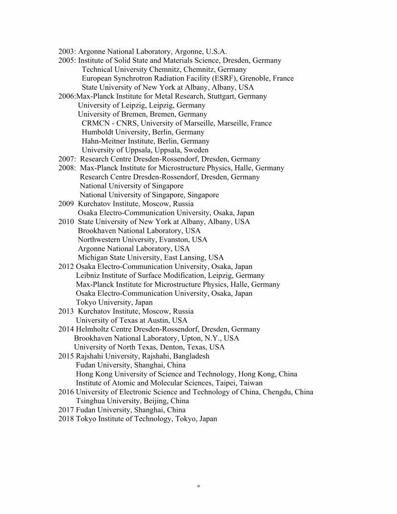
International Collaborations (as principal investigator): (i) Indo-German bilateral collaboration with Hamburg Synchrotron Radiation Laboratory (HASYLAB) at DESY, Hamburg, Germany (Physics-25). (1990-2002) . (ii) Indo-US collaboration with State University of New York at Albany, New York, U.S.A. Grantee: Office of Naval Research, U.S.A. Grant No.N00014-95-1-0130. (1995-2006) (iii) Indo-Japan (DST-JST) collaborative research programme with Osaka Electro-Communication University (2009- 2012) Visits Abroad, Lectures, Seminars: Long visits: [1] Hamburg Synchrotron Radiation Laboratory (HASYLAB) at DESY, Hamburg, Germany. (November 1995 - November 1996), Guest Scientist [2] Helmholtz Center Dresden-Rossendorf, Dresden, Germany EU Guest Scientist (Marie Curie International Incoming Fellow of European Union) (April 2005 - March 2006) Short visits and seminars: 1990 : State University of New York at Albany (SUNYA), New York, U.S.A.
HASYLAB at DESY, Hamburg, Germany 1992: HASYLAB at DESY, Hamburg, Germany 1994: Naval Research Laboratory, Washington DC, U.S.A.
SUNY at Albany, New York, USA 1996: University of Osnabrueck, Osnabrueck, Germany
Max-Planck Institute for Polymer Research, Mainz, Germany 1997: University of Maryland, College Park, U.S.A.
National Institute of Standards and Technology (NIST), U.S.A. Argonne National Laboratory, Argonne, U.S.A. SUNY at Albany, New York, U.S.A.
1999: Ecole Polytechnique, Paris, France Research Centre Dresden-Rossendorf, Dresden, Germany
2000: HASYLAB at DESY, Hamburg, Germany 2002: National University of Singapore, Singapore
Brookhaven National Laboratory, U.S.A. State University of New York at Albany, U.S.A. Paul-Drude Institute, Berlin, Germany University of Bremen, Germany HASYLAB at DESY, Hamburg, Germany
8
2003: Argonne National Laboratory, Argonne, U.S.A. 2005: Institute of Solid State and Materials Science, Dresden, Germany
Technical University Chemnitz, Chemnitz, Germany European Synchrotron Radiation Facility (ESRF), Grenoble, France State University of New York at Albany, Albany, USA
2006:Max-Planck Institute for Metal Research, Stuttgart, Germany University of Leipzig, Leipzig, Germany University of Bremen, Bremen, Germany CRMCN - CNRS, University of Marseille, Marseille, France
Humboldt University, Berlin, Germany Hahn-Meitner Institute, Berlin, Germany University of Uppsala, Uppsala, Sweden
2007: Research Centre Dresden-Rossendorf, Dresden, Germany 2008: Max-Planck Institute for Microstructure Physics, Halle, Germany Research Centre Dresden-Rossendorf, Dresden, Germany National University of Singapore National University of Singapore, Singapore 2009 Kurchatov Institute, Moscow, Russia Osaka Electro-Communication University, Osaka, Japan 2010 State University of New York at Albany, Albany, USA Brookhaven National Laboratory, USA Northwestern University, Evanston, USA Argonne National Laboratory, USA Michigan State University, East Lansing, USA 2012 Osaka Electro-Communication University, Osaka, Japan Leibniz Institute of Surface Modification, Leipzig, Germany Max-Planck Institute for Microstructure Physics, Halle, Germany Osaka Electro-Communication University, Osaka, Japan Tokyo University, Japan 2013 Kurchatov Institute, Moscow, Russia University of Texas at Austin, USA 2014 Helmholtz Centre Dresden-Rossendorf, Dresden, Germany Brookhaven National Laboratory, Upton, N.Y., USA University of North Texas, Denton, Texas, USA 2015 Rajshahi University, Rajshahi, Bangladesh Fudan University, Shanghai, China Hong Kong University of Science and Technology, Hong Kong, China Institute of Atomic and Molecular Sciences, Taipei, Taiwan 2016 University of Electronic Science and Technology of China, Chengdu, China Tsinghua University, Beijing, China 2017 Fudan University, Shanghai, China 2018 Tokyo Institute of Technology, Tokyo, Japan
9
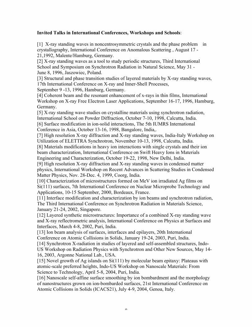
Invited Talks in International Conferences, Workshops and Schools: [1] X-ray standing waves in noncentrosymmetric crystals and the phase problem in crystallography, International Conference on Anomalous Scattering , August 17 - 21,1992, Malente/Hamburg, Germany. [2] X-ray standing waves as a tool to study periodic structures, Third International School and Symposium on Synchrotron Radiation in Natural Science, May 31 - June 8, 1996, Jaszowiec, Poland. [3] Structural and phase transition studies of layered materials by X-ray standing waves, 17th International Conference on X-ray and Inner-Shell Processes, September 9 -13, 1996, Hamburg, Germany. [4] Coherent beam and the resonant enhancement of x-rays in thin films, International Workshop on X-ray Free Electron Laser Applications, September 16-17, 1996, Hamburg, Germany. [5] X-ray standing wave studies on crystalline materials using synchrotron radiation, International School on Powder Diffraction, October 7-10, 1998, Calcutta, India. [6] Surface modification in ion-solid interactions, The 5th IUMRS International Conference in Asia, October 13-16, 1998, Bangalore, India,. [7] High resolution X-ray diffraction and X-ray standing waves, India-Italy Workshop on Utilization of ELETTRA Synchrotron, November 10-13, 1998, Calcutta, India. [8] Materials modifications in heavy ion interactions with single crystals and their ion beam characterization, International Conference on Swift Heavy Ions in Materials Engineering and Characterization, October 19-22, 1998, New Delhi, India. [9] High resolution X-ray diffraction and X-ray standing waves in condensed matter physics, International Workshop on Recent Advances in Scattering Studies in Condensed Matter Physics, Nov. 28-Dec. 4, 1999, Coorg, India. [10] Characterization of microstructures formed on MeV ion irradiated Ag films on Si(111) surfaces, 7th International Conference on Nuclear Microprobe Technology and Applications, 10-15 September, 2000, Bordeaux, France. [11] Interface modification and characterization by ion beams and synchrotron radiation, The Third International Conference on Synchrotron Radiation in Materials Science, January 21-24, 2002, Singapore. [12] Layered synthetic microstructures: Importance of a combined X-ray standing wave and X-ray reflectrometric analysis, International Conference on Physics at Surfaces and Interfaces, March 4-8, 2002, Puri, India. [13] Ion beam analysis of surfaces, interfaces and epilayers, 20th International Conference on Atomic Collisions in Solids, January 19-24, 2003, Puri, India. [14] Synchrotron X-radiation in studies of layered and self-assembled structures, Indo-US Workshop on Radiation Physics with Synchrotron and Other New Sources, May 14-16, 2003, Argonne National Lab., USA. [15] Novel growth of Ag islands on Si(111) by molecular beam epitaxy: Plateaus with atomic-scale preferred heights, Indo-US Workshop on Nanoscale Materials: From Science to Technology, April 5-8, 2004, Puri, India. [16] Nanoscale self-affine surface smoothing by ion bombardment and the morphology of nanostructures grown on ion-bombarded surfaces, 21st International Conference on Atomic Collisions in Solids (ICACS21), July 4-9, 2004, Genoa, Italy.
10
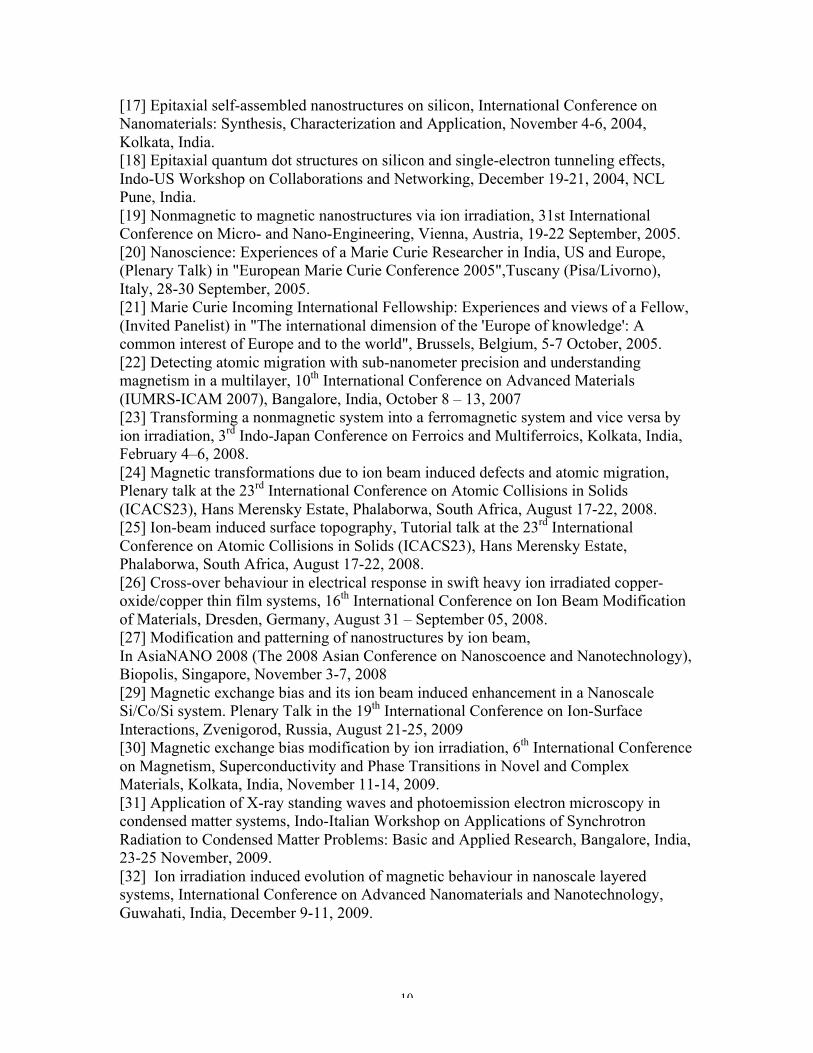
[17] Epitaxial self-assembled nanostructures on silicon, International Conference on Nanomaterials: Synthesis, Characterization and Application, November 4-6, 2004, Kolkata, India. [18] Epitaxial quantum dot structures on silicon and single-electron tunneling effects, Indo-US Workshop on Collaborations and Networking, December 19-21, 2004, NCL Pune, India. [19] Nonmagnetic to magnetic nanostructures via ion irradiation, 31st International Conference on Micro- and Nano-Engineering, Vienna, Austria, 19-22 September, 2005. [20] Nanoscience: Experiences of a Marie Curie Researcher in India, US and Europe, (Plenary Talk) in "European Marie Curie Conference 2005",Tuscany (Pisa/Livorno), Italy, 28-30 September, 2005. [21] Marie Curie Incoming International Fellowship: Experiences and views of a Fellow, (Invited Panelist) in "The international dimension of the 'Europe of knowledge': A common interest of Europe and to the world", Brussels, Belgium, 5-7 October, 2005. [22] Detecting atomic migration with sub-nanometer precision and understanding magnetism in a multilayer, 10th International Conference on Advanced Materials (IUMRS-ICAM 2007), Bangalore, India, October 8 – 13, 2007 [23] Transforming a nonmagnetic system into a ferromagnetic system and vice versa by ion irradiation, 3rd Indo-Japan Conference on Ferroics and Multiferroics, Kolkata, India, February 4–6, 2008. [24] Magnetic transformations due to ion beam induced defects and atomic migration, Plenary talk at the 23rd International Conference on Atomic Collisions in Solids (ICACS23), Hans Merensky Estate, Phalaborwa, South Africa, August 17-22, 2008. [25] Ion-beam induced surface topography, Tutorial talk at the 23rd International Conference on Atomic Collisions in Solids (ICACS23), Hans Merensky Estate, Phalaborwa, South Africa, August 17-22, 2008. [26] Cross-over behaviour in electrical response in swift heavy ion irradiated copper-oxide/copper thin film systems, 16th International Conference on Ion Beam Modification of Materials, Dresden, Germany, August 31 – September 05, 2008. [27] Modification and patterning of nanostructures by ion beam, In AsiaNANO 2008 (The 2008 Asian Conference on Nanoscoence and Nanotechnology), Biopolis, Singapore, November 3-7, 2008 [29] Magnetic exchange bias and its ion beam induced enhancement in a Nanoscale Si/Co/Si system. Plenary Talk in the 19th International Conference on Ion-Surface Interactions, Zvenigorod, Russia, August 21-25, 2009 [30] Magnetic exchange bias modification by ion irradiation, 6th International Conference on Magnetism, Superconductivity and Phase Transitions in Novel and Complex Materials, Kolkata, India, November 11-14, 2009. [31] Application of X-ray standing waves and photoemission electron microscopy in condensed matter systems, Indo-Italian Workshop on Applications of Synchrotron Radiation to Condensed Matter Problems: Basic and Applied Research, Bangalore, India, 23-25 November, 2009. [32] Ion irradiation induced evolution of magnetic behaviour in nanoscale layered systems, International Conference on Advanced Nanomaterials and Nanotechnology, Guwahati, India, December 9-11, 2009.
11
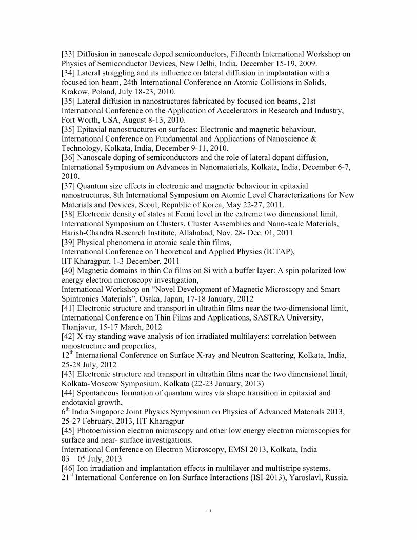
[33] Diffusion in nanoscale doped semiconductors, Fifteenth International Workshop on Physics of Semiconductor Devices, New Delhi, India, December 15-19, 2009. [34] Lateral straggling and its influence on lateral diffusion in implantation with a focused ion beam, 24th International Conference on Atomic Collisions in Solids, Krakow, Poland, July 18-23, 2010. [35] Lateral diffusion in nanostructures fabricated by focused ion beams, 21st International Conference on the Application of Accelerators in Research and Industry, Fort Worth, USA, August 8-13, 2010. [35] Epitaxial nanostructures on surfaces: Electronic and magnetic behaviour, International Conference on Fundamental and Applications of Nanoscience & Technology, Kolkata, India, December 9-11, 2010. [36] Nanoscale doping of semiconductors and the role of lateral dopant diffusion, International Symposium on Advances in Nanomaterials, Kolkata, India, December 6-7, 2010. [37] Quantum size effects in electronic and magnetic behaviour in epitaxial nanostructures, 8th International Symposium on Atomic Level Characterizations for New Materials and Devices, Seoul, Republic of Korea, May 22-27, 2011. [38] Electronic density of states at Fermi level in the extreme two dimensional limit, International Symposium on Clusters, Cluster Assemblies and Nano-scale Materials, Harish-Chandra Research Institute, Allahabad, Nov. 28- Dec. 01, 2011 [39] Physical phenomena in atomic scale thin films, International Conference on Theoretical and Applied Physics (ICTAP), IIT Kharagpur, 1-3 December, 2011 [40] Magnetic domains in thin Co films on Si with a buffer layer: A spin polarized low energy electron microscopy investigation, International Workshop on “Novel Development of Magnetic Microscopy and Smart Spintronics Materials”, Osaka, Japan, 17-18 January, 2012 [41] Electronic structure and transport in ultrathin films near the two-dimensional limit, International Conference on Thin Films and Applications, SASTRA University, Thanjavur, 15-17 March, 2012 [42] X-ray standing wave analysis of ion irradiated multilayers: correlation between nanostructure and properties, 12th International Conference on Surface X-ray and Neutron Scattering, Kolkata, India, 25-28 July, 2012 [43] Electronic structure and transport in ultrathin films near the two dimensional limit, Kolkata-Moscow Symposium, Kolkata (22-23 January, 2013) [44] Spontaneous formation of quantum wires via shape transition in epitaxial and endotaxial growth, 6th India Singapore Joint Physics Symposium on Physics of Advanced Materials 2013, 25-27 February, 2013, IIT Kharagpur [45] Photoemission electron microscopy and other low energy electron microscopies for surface and near- surface investigations. International Conference on Electron Microscopy, EMSI 2013, Kolkata, India 03 – 05 July, 2013 [46] Ion irradiation and implantation effects in multilayer and multistripe systems. 21st International Conference on Ion-Surface Interactions (ISI-2013), Yaroslavl, Russia.
12
22 – 26 August, 2013 [47] Evolution of electronic structure and transport properties of ultrathin films near the 2-D limit. ACCMS-VO8, Tohoku University, Sendai and Matsushima, Japan, 7-9 November, 2013 [48] Electronic structure and transport in atomic layer thin films in the 2D to 3D crossover regime 9th International Symposium on Atomic Level Characterization for New Materials and Devices ’13 (ALC’13), The Big Island, Hawaii, USA, 02-06 December, 2013 [49] Self-organized epitaxial nanostructures on silicon surfaces International Conference in Asia (IUMRS-ICA2013), Bangalore, 16-20 December, 2013 [50] Surface science: An introduction (Tutorial) The 3rd International Conference on Physics at Surfaces and Interfaces (PSI 2014), Puri, India, 24-28 February, 2014 [51] Towards tunable properties via structures in the lower dimensional crossover regimes. The 3rd International Conference on Physics at Surfaces and Interfaces (PSI 2014), Puri, India, 24-28 February, 2014 [52] A spin-polarized low energy electron microscopic investigation of magnetic domains in thin Co films on Si with a buffer layer International Conference on Spin Physics and Nanomagnetism, Max-Planck Institute of Microstructure Physics, Halle, Germany, 10-13 July, 2014 [53] Engineering quantum structures at surfaces International Conference on Emerging Materials: Characterization and Application, Kolkata, India, 4 – 6 December, 2014 (Plenary lecture) [54] Electronic structure and transport in low dimensional structures in the dimensional crossover regimes, 8th India-Singapore Symposium in Condensed Matter Physics, IIT Kanpur, 25-27 February, 2015 [55] Quantum phenomena in nanostructures International Conference on Advances in Physics, Rajshahi, Bangladesh, 18-19 April, 2015 (Plenary lecture) [56] Surfactant role of Ag in an effort to grow germanene on a Si(111)/Ge(√3x√3)-Ag substrate, International Conference on Applied Surface Science, Shanghai, China 27-30 July, 2015 [57] Phenomena in self-organized epitaxial nanostructure growth and structures in the dimensional crossover regimes, EMN (Energy Materials Nanotechnology) Meeting, Hong Kong, 09-12 December, 2015 [58] Growth of epitaxial nanowires using substrate symmetry as well as by symmetry breaking, EMN Meeting on Nanowires (Energy, Materials, Nanotechnology), Amsterdam, Netherlands, 16 – 19 May, 2016 [59] Self-organized epitaxial quantum dots on Si, single electron tunneling and quantum capacitance,
13
International Frontier Forum on Quantum Information 2016, Chengdu, China, 17 – 19 June, 2016 [60] Ion fluence dependent oscillatory amorphization and recrystallization, 27th International Conference on Atomic Collisions in Solids, Lanzhou, China, 24 – 29 July, 2016 [61] Epitaxial, endotaxial and polycrystalline transition metal silicide nanostructures on silicon, Third International Conference on Emerging Electronics (ICEE 2016), IIT Bombay, 27 – 30 December, 2016 [62] Self-organized epitaxial metal silicide nanostructures on silicon surfaces, The 3rd International Conference on Surface and Interface of Materials (SIM2017), Bangkok, Thailand, 3 – 5 January, 2017 [63] Nanoscale transition metal silicides in nanoelectronics, International Conference on Advances in Functional Materials (ICAFM2017), Chennai, India, 6-8 January, 2017 [64] Emerging materials and novel phenomena in thin films, The 2nd International Conference on Emerging Materials: Charatization and Application (EMCA 2017), NIT Durgapur, India, 15-17 March, 2017 [65] Materials and issues in miniaturization in silicon technology towards quantum computers, 1st International Conference on Electronics, Materials Engineering and Nanotechnology (IEMENTech 2017), Kolkata, India, 28 -29 April, 2017 [66] Superdense nonmagnetic cobalt, The 9th International Conference on Materials for Advanced Technologies (ICMAT 2017), Singapore, 18 – 23 June, 2017 [67] Electronic structure of atomic- and nanoscale structures in the dimensional crossover regimes, BIT’s 1st Annual Conference of Quantum World 2017 (CQW 2017), Changsha, China, 16 – 18 October, 2017 [68] Superconductivity in cobalt thin films, 17th International Conference on Thin Films 2017 (ICTF 2017), Delhi, India, 14 -17 November, 2017 [69] Endotaxial silicide nanostructures on silicon and growth induced surface reconstruction, Indo-US Discussion Meeting on Surfaces and Interfaces, Kolkata, India, 02 – 04 January, 2018 [70] Superconducting cobalt in nanoscale cobalt thin films (Keynote lecture), 24th World Congress on Nanomaterials and Nanotechnology, Bangkok, Thailand, 12-13 July, 2018 [71] Scanning tunneling microscopy and photoemission electron microscopy, International Conference on Microscopy and XXXIX Annual Meeting of Electron Microscope Society of India, Bhubaneswar, 18-20 July, 2018 (Pre-conference Workshop) [72] Vital role of transmission electron microscopy in exploring thin films and low dimensional structures, International Conference on Microscopy and XXXIX Annual Meeting of Electron Microscope Society of India, Bhubaneswar, India, 18-20 July, 2018
14
[73] Superconductivity of cobalt in nanoscale cobalt thin films, The 5th Conference on New Advances in Condensed Matter Physics, Kunming, China, 21- 23 August, 2018 [74] Handshake between electronic structure theory and experiment in surface science and nanoscale science (Plenary Lecture), International Workshop on Evolution of Electronic Structure theory & Experimental Realization (FESTER-2018), Chennai, india, 11 -15 September, 2018 [75] Loss of magnetism and emergence of superconductivity in cobalt in a self-organized superconductor-ferromagnet hybrid structure, 20th International Union of Materials Research Societies - International Conference in Asia (IUMRS-ICA 2019), Perth, Australia, 22-26 September 2019. [76] Early stage of growth of epitaxial FeSi2 nanowires on Si(110) surface, The 20th International Workshop on the Physics of Semiconductor Devices (IWPSD 2019), Kolkata, India, 17 – 20 December, 2019. Invited talks in national conferences/symposia/workshops: [1] Application of X-ray standing waves to the structural determination of the adsorbate covered crystal surfaces, Solid State Physics Symposium of DAE (India), Dec. 27-30, 1985, Nagpur,India. [2] Structure_property relation in surfaces and interfaces, XXI National Seminar on Crystallography, Dec. 27-29, 1989, Bombay, India . [3] Structural investigations of epitaxial interfaces, DAE Solid State Physics Symposium, Dec. 21-24, 1991, Varanasi, India. [4] Surface and interface studies with X-ray standing waves, National Conference on Science and Technology of Surfaces and Interfaces, Dec. 16-18, 1996, Kharagpur, India. [5] Strain relaxation, self-organization and defects in epitaxial growth, DAE Solid State Physics Symposium,Dec. 27 -31, 1997, Cochin, India. [6] Institute of Physics 3 MV 9SDH-2 Pelletron: Present status, Conference on Physics and Technology of Accelerators, February 10-13, 1998, Calcutta, India. [7] Multilayers characterization by X-ray standing waves, Workshop on Interface Engineering by Energetic Heavy Ions, April 3-4, 2000, IIT, Kanpur. [8] Multidisciplinary research at the 3 MV ion accelerator centre at IOP, DAE Solid State Physics Symposium, December 27 - 31, 2000, Bilashpur. [9] The ion microbeam facility in Bhubaneswar, Conference on Accelerator based research in basic and applied sciences, February 25-27, 2001, New Delhi. [10] Nanostructured multilayers - microstructures and ion beam induced effects, Symposium on New Developments in Materials: Nanomaterials and Manganites, March 2-3, 2001, New Delhi. [11] Ion beam characterization of thin films, Indian Vacuum Society Symposium, September 5-7, 2001, Bangalore. [12] Surface and interface phenomena and self-assembled nanostructures. (2003 MRSI Medal Lecture) 14th Annual General Meeting of Materials Research Society of India, 11-13 February, 2003, BARC, Mumbai.
15
[13] Ion beam analysis and modi_cations of surfaces, interfaces and layered materials. Workshop on Utilization of Energetic Ion Beams for Materials Research, July 29-31, 2003, Kalpakkam. [14] Growth of self-assembled nanostructures by molecular beam epitaxy and their characterizations by scanning tunneling microscopy and spectroscopy. INAE conference on Nanotechnology (ICON-2003), December 22-23, 2003, Chandigarh. ( with a large international participation) [15] MBE-grown self-assembled nanostructures and single-electron tunneling, MRSI Symposium on Nano and Biotechnology, August 7, 2004, Kharagpur. [16] Self-assembled nanostructures on silicon: Growth and quantum phenomena, National Conference on Current Trends in Condensed Matter Research, September 20-22, 2004. Kakatiya University, Warangal. [17] Epitaxial structures on single crystal surfaces, 54th DAE Solid State Physics Symposium, Vadodara, December 14-18, 2009. [18] Morphology and electronic structure of surface-based epitaxial nanostructures, Condensed Matter Days: Symposium on Condensed Matter Physics, Kalyani, August 25-27, 2010. [19] Quantum size effect in electronic and magnetic behaviour in epitaxial nanostructures, Current Trends in Condensed Matter Physics, Bhubaneswar, December 15-19, 2010. [20] Science at the atomic scale, National Conference on Recent Advances in Condensed Matter Physics, Aligarh, March 14-15, 2011. [21] Nanoscale structures towards future information and communication technologies. DST TIFAC Meeting – Vision 2035, Bose Institute, Kolkata, 6 June, 2011 [22] Ion beams - a versatile tool for materials modification, Recent Advances in Mechanics and their Application in Nano Engineering and Technology, Itanagar, 1-12 August, 2011 [23] Magnetism in ultrathin layers and ion beam induced effects National School cum Workshop on Magnetic Phase Transitions and Transformations, UGC-DAE CSR and Jadavpur University, Kolkata, 3-9 August, 2011 [24] Ordered self-organization and fabrication of nanostructures by ion beams. DAE-BRNS Theme Meeting on Emerging Trends in Applications of Lasers and Accelerators in Nanomaterials, BARC, Mumbai, 20-21 October, 2011 [25] Growth of epitaxially oriented nanoscale Ag islands on oxidized Si substrates: Influence of short range order on the oxide surface. Indian Vacuum Society Symposium on Thin Films: Science and Technology, BARC, Mumbai, 9-12 November, 2011 [26] Scanning tunneling microscopy, photoemission electron microscopy and spin polarized low energy electron microscopy Workshop on Electron Microscopy, Institute of Physics, Bhubaneswar, 22-25 November, 2011 [27] Pattern formation and electronic structure in atomic scale thin films Conference on “Advanced Functional Materials”, S. N. Bose Centre, Kolkata, 1-2 March, 2012 [28] How does the electronic structure change as a material is thinned down to one atomic layer?
16
First National Seminar on Recent Trends in Condensed Matter Physics Including Laser Applications, Burdwan University, 6-7 March, 2012 [29] Standing waves of X-rays and their diverse applications in condensed matter physics and materials science S. P. Sengupta Memorial Lecture of Material Society of India, Kolkata Chapter. 08 June, 2012 [30] Wonders in the ultrathin materials world, In the C.V. Raman Session on Materials Science, 100th Indian Science Congress 03-07 January, 2013) [31] Radiations in modification and analysis of materials, National Workshop on Applications of Radiationin Physical, Chemical and Life Sciences, 04 – 06 September, 2013 [32] Probing Materials with ion beams, National Short Term Course on Modern Methods in Materials Processing and Characterization, NIT Durgapur, 17 -19 September, 2013 [33] Quantum structures and phenomena – An emerging perspective, Special invited lecture in Multiscale Modeling of Materials and Devices (MMMD-2014), BARC, Mumbai, 30 Oct. – 02 Nov., 2014 [34] Novel structures on surfaces in the dimensional crossover regimes, National Conference on Current Trends in Advanced Materials (CTMat-2014), VECC, Kolkata, 19-21 November, 2014 [35] Induced substrate strain in heteroepitaxial growth Advances in Nanomaterials using Synchrotron Techniques (ANST-2014) Kolkata, 11-13 December, 2014 [36] Quantum structures and phenomena – an emerging perspective 26th Annual General Meeting, Materials Research Society of India, Jaipur, 9-11 February, 2015 [37] Quantum nanoelectronics Keynote lecture in National Conference on Micro and Nano Electronic Systems and Devices (MINO-III), Jaipur, 20-21 March, 2015 [38] Slimming single crystals to fitness: Making them active, functional and beautiful, SERC School on “Single Crystals of Functional Materials and their Applications”, SSN College of Engineering, Chennai, 02-22 September, 2015 [39] Playing with atoms for future technology, West Bengal State Level Student Youth Science Fair, Kolkata, 05 October, 2015 [40] Multilayered structures in space research and the effect of their exposure to energetic ions in space, Discussion Meeting on Materials Science Related to Nuclear and Space Research and Industry, SINP, Kolkata, 06-07 October, 2015 [41] Applications of energetic Ion beams in condensed matter physics and materials science, Workshop on the Use of Low Energy Ion Beams, Institute of Physics, Bhubaneswar, 07-09 November, 2015 [42] Standing waves of X-rays and their diverse applications in condense matter physics, Conference on “Synchrotron Radiation: Application to Condensed Matter Physics”,
17
IISER, Kolkata, 09 January 2016 [43] Quantum structures and phenomena – An emerging perspective, Solid State Physics Day, IACS, Kolkata, 12 January, 2016 [44] Self-organized quantum structures: Growth, electronic structure and transport, Discussion Meeting on Nano-scale and Atomic-scale Quantum Structures and Devices, IACS, Kolkata, 16-17 February, 2016 [45] Demise of Moore’s law and the beginning of the quantum era (Keynote Lecture), National Conference on Advancement in Frontier Physics: From 20th Century to the Present, Bhairab Ganguly College, Kolkata, 26-27 February, 2016 [46] Growth of self-organized quantum structures by molecular beam epitaxy and reactive deposition epitaxy, Conference on Emerging Materials (CEMAT 2016), Bengaluru, 18 – 19 July, 2016 [47] Seeing atoms and playing with atoms leading to future nanotechnologies, (Keynote lecture). National Workshop on Advances in Physics, Patna University, 8 - 9 July, 2016 [48] Advanced nanotechnology from atomic scale growth and atom manipulation, (Keynote lecture). National Conference on Recent Advances in Nanoscience and Nanotechnology (NCRANNT2016), Nehu, Shillong, 8 – 9 September, 2016 [49] Superdense nonmagnetic cobalt, Silver Jubilee Research Conference on “Study of matter using intense radiation sources and under extreme conditions”, UGC-DAE CSR, Indore, 3 – 6 November, 2016 [50] Real time investigation of the effect of thermal expansion coefficient mismatch on film-substrate strain partitioning in epitaxial systems, Discussion Meeting on Synchrotron Techniques in Materials Research, Dooars, 2-5 February, 2017 [51] Twist and turn in magnetism, Seminar “Twist and Turn in Physics Research: Special Emphasis on Bio- and Condensed Matter Physics”, Jadavpur University, Kolkata, 21-22 February, 2017. [52] Solid state quantum structures in quantum information processing and quantum technology, Discussion Meeting on Quantum Optics and Quantum Technology (QOQT 2017), Kolkata, 5 – 8 June, 2017 [53] X-ray and neutron scattering in thin films: Reflectivity, standing waves and resonance enhancement, Theme Meeting on Neutron Scattering, Mumbai, 19 August, 2017 [54] Superconductivity in cobalt, 9th Vidyasagar-Satyendranath Bose National Workshop 2018 on Science of Materials: Challenges and Prospects (SMCP- 2018), Vidyasagar University, Midnapore,17-19 Jan 2018, [55] Quantum tunneling in nature, life and lifestyle UGC-DAE CSR Indore Centre Research Scholars’ Workshop, Indore, 03-06 October, 2018. [56] Perspectives of surface and interface science 10th Vidyasagar-Satyendranath Bose National Workshop on Expanding Horizon in Physics, Vidyasagar University, Midnapore, 16-22 January, 2019 (Keynote lecture) [57] Epitaxial metallic nanowires on semiconductors
18
National Conference on Recent Developments in Nanoscience & Nanotechnology, Kolkata, 29-31 January, 2019. [58] Perspectives of surface and interface science Conference on Recent Advances in Physics, Delhi University, Delhi, 27 February, 2019. [59] Transition metal silicide nanowires on silicon: Epitaxial growth, self-organization and shape transition, The 64th DAE Solid State Physics Symposium, Jodhpur, 18 – 22 December, 2019. [60] Novel magnetic behaviour and inhomogeneous superconductivity in cobalt thin films with high density cobalt layers, 2nd Indian Materials Conclave and 31st Annual General Meeting of MRSI, Kolkata, 11-14 February, 2020. [61] Quantum phenomena in surface science National Conference on Frontiers of Materials Science and Photonics: Issues and Developments, SKB University, Purulia, 5 -6 March, 2020. Conference Organization: [1] Organized (Convener) several National Workshops over the years [2] Organized (Convener) " The 1st International Conference on Physics at Surfaces and Interfaces", March 2002, Puri, India [3] Organized ( as Co-Chairman with Prof. A. P. Pathak) the "20th International Conference on Atomic Collisions in Solids", January 19-24, 2003, Puri, India (In the history of four decades of this conference this is the first time it was held in India. Previous two conferences were held in France and Denmark). [4] Organized (as Co-Chairman) the "18th International Conference on Ion Beam Analysis" in 2007. (held for the first time in India). [5] Organized (Convener) "The 2nd International Conference on Physics at Surfaces and Interfaces", February 23-27, 2009, Puri, India [6] Organized (Co-Chairman) "The 3rd International Conference on Physics at Surfaces and Interfaces", February 24-28, 2014, Puri, India Current research interest: (i) Epitaxial layers, molecular beam epitaxy (MBE) and self-organized epitaxial growth and properties of nanostructures. Quantum structures. (ii) Ion-solid interaction, surface and interface modification by ion irradiation. (iii) Utilization of synchrotron radiation in surface and nanoscale science. (iv) Structure, morphology and properties of thin films, surfaces and interfaces. (v) Layered synthetic nanostructural multilayers and their ion-beam modification. (vi) Magnetism in nanoscale structures, superconductivity (vii) Scanning tunneling microscopy and spectroscopy, photoemission electron microscopy, X-ray and neutron reflectrometry, X-ray standing wave
19
LIST OF PUBLICATIONS: A. Books or Chapters in a Book: 1. Physics at Surfaces and Interfaces
Edited by B. N. Dev (World Scientific, Singapore, 2003) 2. Nuclear Instruments and Methods in Physics Research, Section B
Vol. 212, 2003 (North Holland, The Netherlands) Edited by A. P. Pathak and B. N. Dev Proceedings of the 20th International Conference on Atomic Collisions in Solids (ICACS20, January 19-24, 2003, Puri, India)
3. RBS and Channeling Analysis of Self-Assembled Structures,
B. N. Dev, A chapter in the book Ion Beam Analysis of Surfaces and Interfaces of Condensed Matter Systems, (NOVA Science Publishers Inc., New York, 2003), Ed P. Chakraborty, pp.103- 135.
4. Novel growth of Ag islands on Si(111) surfaces by molecular beam epitaxy: Plateaus with atomic scale preferred heights, D. K. Goswami, K. Bhattacharjee and B. N. Dev, in Nanoscale Materials: From Science and Technology, Editors: S. N. Sahu, R. K. Choudhury and P. Jena 5. Nuclear Instruments and Methods in Physics Research, Section B
Vol.266, 2008 (Elsevier) Edited by A. P. Pathak, D. K. Avasthi and B. N. Dev Proceedings of the 18th International Conference on Ion Beam Analysis (IBA2007, September 23-28, 2007, Hyderabad, India)
6. Applied Surface Science, Vol. 256, No.2, 2009 (Elsevier) Edited by B. N. Dev and P. V. Satyam Proceedings of the 2nd International Conference on Physics at Surfaces and Interfaces (Puri, India, 23-27 February, 2009)
7. Defect induced magnetism in fullerines and MoS2
Sinu Mathew, T. K. Chan, B. N. Dev, John TL Thong, M. B. H. Breese, T. Venkatesan in the book Low Power Semiconductor Devices and Processes for Emerging Applications in Communications, Computing, and Sensing,
S. Walia (Ed), (CRC Press, 2018) pp 79 – 93. 8. High-density nonmagnetic cobalt in cobalt thin films B. N. Dev and Nasrin Banu
20
in the book Recent Advances in Thin Film Research, Materials Horizons: From Nature to Nanomaterials, Sushil Kumar and D. K. Aswal (Eds), (Springer Nature, 2020) pp. 103 – 130. 9. Writing an invited monograph on
Solid Surfaces and Nanostructures as a part of a series on Science and Technology of Atomic, Molecular, Condensed Matter and Biological Systems to be published by Elsevier Science, The Netherlands. Series Editor: Professor T. P. Das (State University of New York at Albany, USA).
B. Refereed Journals [1] First-principles investigation of location and electronic structure of adsorbed halogen atoms on semiconductor surfaces, B.N.Dev, K.C.Mishra, W.M. Gibson and T.P.Das, Phys. Rev. B29, 1101 (1984). (Rapid Commun.) [2] Investigation of electronic structure and associated nuclear quadrupole interaction of adsorbed fluorine atoms on silicon surface, K.C.Mishra, B.N.Dev, S.M.Mahapatra, W.M.Gibson and T.P.Das, Hyperfine Interactions 15/16, 997 (1983). [3] An X-ray standing wave interface spectrometric analysis of chemisorption of selenium on silicon (111) and (220) surfaces, B.N.Dev, T.Thundat and W.M. Gibson, J. Vac. Sci. Technol. A3, 946 (1985). [4] An X-ray standing wave interference spectrometric analysis of bromine on cleaved silicon from solution , B.N.Dev, V.Aristov, N.Hertel, T.Thundat and W.M. Gibson, J. Vac. Sci. Technol. A3, 975 (1985). [5] Chemisorption of bromine on cleaved silicon (111) surfaces : An X-ray standing wave interference spectrometric analysis, B.N.Dev, V.Aristov, N.Hertel, T.Thundat and W.M.Gibson, Surf. Sci. 163, 457 (1985). [6] First-principles investigation of geometric and electronic structure of aluminium adsorbed on silicon surface, B.N.Dev, S.M.Mahapatra, K.C.Mishra, W.M.Gibson and T.P.Das, Phys. Rev. B36, 2666 (1987). [7] X-ray standing wave studies of germanium adsorbed on Si(111) surfaces , B. N.Dev, G.Materlik, R.L.Johnson, W.Kranz and P.Funke,
21
Surf. Sci. 178, 1 (1986). [8] Geometrical structures of the Ge/Si(111) interface and the Si(111)(7x7) surfaces, B.N.Dev, G.Materlik, F.Grey, R.L.Johnson and M.Clausnitzer, Phys. Rev. Lett. 57, 3058 (1986); Phys. Rev. Lett. 59, 1790 (1987) [9] Geometric structure of the NiSi2-Si(111) interface: An X-ray standing wave analysis , E.Vlieg, A.E.M.J.Fischer, J.F van der Veen, B.N.Dev and G.Materlik, Surf. Sci. 178, 36(1986). [10] First principle investigation of moderately heavy atoms on semiconductor surfaces_ bromine on silicon, S.M.Mahapatra, N.Sahoo, K.C.Mishra, B.N.Dev, W.M.Gibson and T.P.Das , J. Vac. Sci. Technol. A4, 2441 (1986). [11] Nuclear quadrupole interaction associated with adsorbed halogen and chalcogen atoms at semiconductor surfaces, S.M.Mahapatra, N.Sahoo , K.C.Mishra, B.N.Dev, W.M.Gibson and T.P.Das, Hyperfine Interactions 34, 581 (1987) [12] High temperature X-ray standing wave study : Application to melting of monolayers of Pb on Ge(111)surfaces, B.N.Dev, F.Grey, R.L.Johnson and G.Materlik, Europhys. Lett. 6, 311 (1988). [13] Coherent X_ray scattering by phonons: Determination of phonon eigenvectors, H.Spalt, A.Zounek, B.N.Dev and G.Materlik, Phys. Rev. Lett. 60, 1868(1988); Phys. Rev. Lett. 61, 2819 (1988). [14] Investigation of location, electronic structures and associated properties of chalcogen atoms adsorbed on silicon surfaces: Sulfur and selenium, S.M.Mahapatra, B.N.Dev, K.C.Mishra, W.M.Gibson and T.P.Das, Phys. Rev. B38, 13335 (1988). [15] Investigation of electronic structures and associated properties including hyperfine interactions for halogen adsorbed silicon surfaces: Fluorine through iodine, S.M.Mahapatra, B.N.Dev, K.C.Mishra, N.Sahoo, W.M.Gibson and T.P.Das, Phys. Rev. B38, 12556 (1988). [16] Experimental and theoretical investigations of chemisorbed Ga on Si(111), T.Thundat, S.M.Mahapatra, B.N.Dev, W.M.Gibson and T.P.Das, J. Vac. Sci. Technol. A6, 681 (1988). [17] Comment on "Quantitative structural determination of metallic film grown on semiconductor crystal: (√3x√3)R30˚→ (1x1) Pb on Ge(111)", B.N.Dev,
22
Phys. Rev. Lett. 64, 1182 (1990). [18] Electronic structure and associated properties of adsorbed atoms on silicon surfaces including hyperfine interactions, S.M.Mahapatra, B.N.Dev, L.Luo, T.Thundat, W.M.Gibson, K.C.Mishra, N.Sahoo and T.P.Das, Revs. of Solid State Science, Vol.4, pp 873-900 (1990) (World Scientific). [19] Compton Scattering study of the electronic structure of CuO , K.Sekar, B.K.Panda, B.N.Dev and D.P.Mahapatra, J. Phys. Condens. Matt. 3, 6033 (1991). [20] An RBS study on the annealing behaviour of Cu thin films on brominated Si(111) substrates, K. Sekar, P.V.Satyam, G.Kuri, D.P.Mahapatra and B.N.Dev, Nucl. Instr. and Meth. B71, 308 (1992). [21] An RBS study of interdiffusion across a brominated Si(111)/Cu interface with and without a barrier layer, K.Sekar, P.V.Satyam, G.Kuri, D.P.Mahapatra and B.N.Dev, Nucl. Instr. and Meth. B73, 63 (1993). [22] MeV He++ irradiation induced effects in CuO, K.Sekar, P.V.Satyam, D.P.Mahapatra, B.N.Dev, N.C.Mishra, B.S.Acharya and P.Sen, Nucl. Instr. and Meth. B83, 140 (1993). [23] Location of Ti atoms diffused into nearly perfect crystals of LiNbO3: An X-ray standing wave study , Th.Gog, T.Harasimowicz, B.N.Dev and G.Materlik, Europhys. Lett. 25, 253 (1994). [24] X-ray photoelectron spectroscopic study of Si(100) and Si(111) surfaces with chemically adsorbed bromine, K.Sekar, G.Kuri, D.P.Mahapatra, B.N.Dev, J.V.Ramana, Sanjiv Kumar and V.S.Raju, Surf. Sci. 302, 25 (1994) [25] A high energy ion scattering facility for condensed matter physics and material science studies, K.Sekar, P.V.Satyam, G.Kuri, B.Sundaravel, D.P.Mahapatra and B.N.Dev, Ind. J. Phys. 68A, (1994) p1-22 . [26] X-ray standing wave studies of the properties of ion beam synthesized epitaxial Si/CoSi2/Si system, P.V.Satyam and B.N.Dev, Ind. J. Phys. 68A, 23 (1994).
23
[27] Shape transition in the epitaxial growth of gold silicide in Au thin films on Si(111), K.Sekar, P.V.Satyam, G.Kuri, B.Sundaravel, D.P.Mahapatra and B.N.Dev, Phys. Rev. B51, 14330 (1995). [28] A PC-based control and data acquisition for X-ray reflection measurements , P.V. Satyam and B.N.Dev, Ind. J. Phys. 69A, 415 (1995). [29] Growth and alignment of gold silicide islands on Br-passivated vicinal Si(111) surfaces, K.Sekar, G.Kuri, P,V.Satyam, B.Sundaravel, D.P.Mahapatra and B.N.Dev, Surf. Sci. 339, 96 (1995). [30] A high precision technique using X-ray reflectivity for measurement of surface and interface roughness, P.V.Satyam, S.K.Ghose, D.Bahr, G.Kuri, B Sundaravel, B.Rout and B.N.Dev, Curr. Sci. 69, 526 (1995). [31] Epitaxy driven fractal growth, K.Sekar, P.V.Satyam, G.Kuri, D.P.Mahapatra and B.N.Dev, Solid State Commun. 96, 871 (1995). [32] MeV As and Au ion implantation in Si, GaP, GaAs, InSb and LiNbO3 : Study of range and lattice location, G.Kuri, B.Sundaravel, B.Rout, D.P.Mahapatra and B.N.Dev, Nucl. Instr. Meth. B 111, 234 (1996). [33] Ion channeling studies for the determination of orientation of interface in ion beam synthesized Si/CoSi2/Si system, P. V. Satyam, K. Sekar, G. Kuri, B. Sundaravel, S. K. Ghose, B. Rout, D. P. Mahapatra and B. N. Dev, Indian J. Phys. 70A, 777 (1996). [34] Defects in the ion-beam-synthesized epitaxial Si/CoSi2/Si(111) system. P. V. Satyam, K. Sekar, G. Kuri, B. Sundaravel, D. P. Mahapatra and B. N. Dev, Philos. Mag. Lett. 73, 309 (1996). [35] A simple program to simulate Rutherford backscattering spectra, G. Kuri, K. Sekar, P. V. Satyam, D. P. Mahapatra and B. N. Dev Ind. J. Phys. 70A, 465 (1996). [36] Channeling studies on self-assembled Au4Si islands on Br-passivated Si(111) surfaces , B. Sundaravel , K. Sekar, P. V. Satyam, G. Kuri, B. Rout, S. K. Ghose, D. P. Mahapatra and B. N. Dev, Ind. J. Phys. 70A, 687 (1996).
24
[37] Effect of MeV Au ion implantation on the composition of GaAs upon vacuum annealing : PIXE and XRF studies , G. Kuri, B. Sundaravel, B. Rout, D. P. Mahapatra and B. N. Dev, Nucl. Instr. Meth. B119, 403 (1996). [38] Grazing incidence X-ray standing wave: a novel technique for measuring ultrasmall diffusion coefficients in polymers, S. Dev (nee Sen) and B. N. Dev, Ind. J. Phys 70 A,189 (1996). [39] Determination of strain in a buried epitaxial CoSi2 layer in Si(111) by MeV ion scattering and x-ray rocking curve methods, P. V. Satyam, B. Sundaravel, S. K. Ghose, B. Rout, K. Sekar, D. P. Mahapatra and B. N. Dev, Ind. J. Phys. 70A, 783 (1996). [40] Rutherford backscattering spectrometry and channeling studies on MeV Au-implanted GaAs(100) crystals, G. Kuri, B. Sundaravel, D. P. Mahapatra and B. N. Dev, Nucl. Instr. Meth. B129, 35 (1997). [41] Ion dechanneling studies of defects in an ion-beam-synthesized epilayer sandwich system : Si(111)/CoSi2/Si P. V. Satyam, K. Sekar, G. Kuri, B. Sundaravel, D. P. Mahapatra, and B. N. Dev, Appl. Surf. Sci., 125, 173 (1998) [42] X-ray standing wave and ion scattering studies on Au-implanted LiNbO3(0001) single crystals, B. N. Dev, G. Kuri, P. V. Satyam, B. Sundaravel, Th. Gog and G. Materlik, Appl. Surf. Sci., 125, 163 (1998) [43] Characterization of a liquid-phase-epitaxy-grown Al0:2Ga0:8As film on a GaAs(111) substrate by RBS,channeling and PIGE analyses, G. Kuri, P. V. Satyam, B. Sundaravel, K. Sekar, D. P. Mahapatra and B. N. Dev, Nucl. Instr. and Meth. B140, 229 (1998). [44] Lattice Strain Measurement of Strained In0:1Ga0:9As=GaAs heterostructures by RBS and Channeling, Azher M. Siddiqui, Anand P. Pathak, B. Sundaravel, Amal K. Das, K. Sekar, B.N. Dev and B.M. Arora, Nucl. Instr. and Meth B142, 387 (1998). [45] Micro ion-beam facility at the Institute of Physics, Bhubaneswar, B. Rout, S. K. Ghose, B. Sundaravel, G. Kuri, D. P. Mahapatra, B. N. Dev, P. Sen, H. Bakhru and A. W. Haberl,
25
Radiat. Phys. Chem. 51, 677 (1998). [46] High energy Ni implantation in InP, T. K. Chini, S. R. Bhattacharya, D. Basu, B. Rout, S. Ghose, B. Sundaravel, B. N. Dev, F. Okuyama, M. Kaneko, J. Mater. Sci. Lett. 17, 1117 (1998). [47] Epitaxial growth of Ag on Br-passivated Si(111) under high vacuum, B. Sundaravel, Amal K. Das, S. K. Ghose, K. Sekar and B. N. Dev, Appl. Surf. Sci. 137, 11 (1999). [48] XPS and SIMS analysis of gold silicide grown on a bromine passivated Si(111) substrate, B. Sundaravel, K. Sekar, G. Kuri, P. V. Satyam, B. N. Dev, Santanu Bera and S. V. Narasimhan, P. Chakraborty and F. Caccavale, Appl. Surf. Sci. 137, 103 (1999). [49] High energy high dose Si implantation into Ge and effect of subsequent thermal annealing, G. Kuri, D. P. Mahapatra and B. N. Dev, Rad. Eff. Defects in Solids, 147, 133 (1999). [50] Materials modifications in heavy ion interactions with single crystals and their ion beam characterization, B. N. Dev, Nucl. Instr. and Meth. B156, 258 (1999). [51] Improvement of Ag(111) epitaxy on Si(111) by MeV Si+ irradiation and ion microbeam analysis of thermally induced morphology, B. Sundaravel, Amal K. Das, S. K. Ghose, B. Rout and B. N. Dev, Nucl. Instr. and Meth. B156, 130 (1999). [52] Radiation damage and surface modification of GaAs(001) by MeV C+ and C2+ co-implantation with Ga2+, S. K. Ghose, G. Kuri, Amal K. Das, B. Rout D. P. Mahapatra and B. N. Dev, Nucl. Instr. and Meth. B156, 125 (1999). [53] Resonance enhancement of X-rays in layered materials: Application to surface enrichment in polymer blends, B. N. Dev, Amal K. Das, S. Dev, D. W. Schubert, M. Stamm and G. Materlik, Phys. Rev. B61, 8462 (2000). [54] Spontaneous nanostructural island formation and layer-to-island mass transport in Ge layers on Si(111) surfaces, Amal K. Das, S. K. Ghose, B. N. Dev, G. Kuri and T. R. Yang, Appl. Surf. Sci. 165, 260 (2000).
26
[55] Self-assembled gold silicide wires on bromine-passivated Si(110) surfaces, B. Rout, B. Sundaravel, Amal K. Das, S. K. Ghose, K. Sekar, D. P. Mahapatra and B. N. Dev, J. Vac. Sci. Technol. B18, 1847 (2000). [56] Aspects of surface and interface characterizations by X-rays: The research programme at IOP, Bhubaneswar, B. N. Dev, (invited article) Curr. Sci. 78, 1511 (2000). [57] Self-assembled Ge nanostructures on polymer-coated silicon: growth and characterization, Amal K. Das, J. Kamila, B. N. Dev, B. Sundaravel and G. Kuri, Appl. Phys. Lett. 77, 951 (2000). [58] Surface and near-surface modifications and analysis by MeV ions, B. N. Dev, (invited article) Curr. Sci. 80, 1550 (2001). [59] Response to "Comment on Self-assembled Ge nanostructures on polymer-coated silicon: Growth and Characterization", Amal K. Das, J. Kamila, B. N. Dev, B. Sundaravel and G. Kuri, Appl. Phys. Lett. 78, 3552 (2001). [60] X-ray Standing wave and reflectometric characterization of multilayer structures, S. K. Ghose and B. N. Dev, Phys. Rev. B63, 245409 (2001). [61] Ion-irradiation induced mixing, interface broadening and period dilation in Pt/C multilayers, S. K. Ghose, D. K. Goswami, B. Rout, B. N. Dev, G. Kuri, and G. Materlik, Appl. Phys. Lett. 79, 467 (2001). [62] Status of ion microbeam facility at the Institute of Physics, Bhubaneswar, India, B. Rout, S. K. Ghose, D. P. Mahapatra, B. N. Dev, H. Bakhru and A. W. Haberl, Nucl. Instr. Meth. B181, 110 (2001). [63] Characterization of microstructures formed on MeV ion-irradiated silver films on Si(111) surfaces, B. Rout, J. Kamila, S. K. Ghose, D. P. Mahapatra and B. N. Dev, Nucl. Instr. Meth. B181, 268 (2001). [64] Resonance enhancement of X-rays and fluorescence yield from marker layers in the thin films, S. K. Ghose, B. N. Dev and Ajay Gupta,
27
Phys. Rev. B 64, 233403 (2001). [65] Redistribution of Ni implanted into InP, T. K. Chini, S. K. Ghose, B. Rout, B. N. Dev, M. Tanemura and F. Okuyama, Eur. Phys. J. AP 13, 83 (2001) [66] Clustering in Pb thin films on Si(111) and Pb-induced Si surface ordering, B. Rout, J. Kamila, M. Rundhe and B. N. Dev, Nucl. Instr. Meth. B 190, 641 (2002). [67] Ion beam studies in strained layer superlattices, A. P. Pathak, .....B. N. Dev and A. Turos, Nucl. Instr. Meth. B 193, 319 (2002). [68] Self-assembled growth of nanostructural Ge islands on bromine-passivated Si(111) surface at room temperature, Amal K. Das, B. N. Dev, B. Sundaravel, E. Z. Luo, J. B. Xu and I. H. Wilson, Pramana - J. Phys. 59, 133 (2002). [69] Growth of self-assembled nanostructures by molecular beam epitaxy. D. K. Goswami, B. Satpati, P. V. Satyam and B. N. Dev, Curr. Sci. 84, 903 (2003). [70] Crater formation in gold nano-islands due to MeV self-ion irradiation. P. V. Satyam, J. Kamila, S. Mohapatra, B. Satpati, D. K. Goswami, B. N. Dev, R. E. Cook, L. Assou_d, J. Wang and N. C. Mishra. J. Appl. Phys. 93, 6399 (2003). [71] Nanoscale self-affine smoothing by ion bombardment. D. K. Goswami and B. N. Dev, Phys. Rev. B 68, 033401 (2003). [72] Low current MeV Au2+ ion-induced amorphization in silicon: Rutherford backscattering spectrometry and transmission electron microscopy study. J. Kamila, B. Satpati, D. K. Goswami, M. Rundhe, B. N. Dev and P. V. Satyam Nucl. Instr. Meth. B 207, 291 (2003). [73] Ion irradiation induced impurity redistribution in Pt/C multilayers S. Bera, D. K. Goswami, K. Bhattacharjee and B. N. Dev, Nucl. Instr. Meth. B 212, 530 (2003) [74] Clustering in Pb thin films on bromine-passivated Si(111) surfaces. M. Rundhe, S. Mathew, B. R. Sekhar and B. N. Dev, Nucl. Instr. Meth. B 212, 314 (2003)
28
[75] Observation of smoothing and self-affine fractal roughness on MeV ion-irradiated Si surfaces, D. K. Goswami and B. N. Dev Nucl. Instr. Meth. B 212, 253 (2003). [76] Ion beam characterization and engineering of strain in semiconductor multilayers, S. V. S. Nageswara Rao, A.P. Pathak, A.M. Siddiqui, D. K. Avasthi, C. Muntele, D. Ila, B. N. Dev, R. Muralidharan, F. Eichhorn, R. Groetzschel and A. Turos, Nucl. Instr. Meth. Phys. Res. B 212, 442 (2003). [77] Study of sputtered particles from gold nanoislands due to MeV self-ion irradiation, B. Satpati, D. K. Goswami, S. Roy, T. Som, B. N. Dev and P. V. Satyam, Nucl. Instr. Meth. B 212, 332 (2003). [78] Energy spike induced effects in MeV ion irradiated nanoislands, B. Satpati, D. K. Goswami, U. D. Vaishnav, T. Som, B. N. Dev and P. V. Satyam, Nucl. Instr. Meth. B 212, 157 (2003). [79] Swift heavy ion induced interface modification in Ni/Ge, T. Som, B. Satpati, P. V. Satyam, D. Kabiraj, P. Ayyub, S. Ghosh, Ajay Gupta, B. N. Dev and D. K. Awasthi, Nucl. Instr. Meth. B. 212, 206 (2003) [80] Understanding the quantum size effects in ZnO nanocrystals, Ranjani Viswanatha, Sameer Sapra, B. Satpati, P. V. Satyam , B. N. Dev, and D. D. Sarma, J. Mater. Chem. 14, 661 (2004). [81] Ion-beam-induced embedded nanostructures and nanoscale mixing. B. Satpati, P.V. Satyam, T. Som and B.N. Dev, J. Appl. Phys. 96, 5212 (2004). [82] Synthesis and Characterization of Mn doped ZnO Nanocrystals, Ranjani Viswanatha, Sameer Sapra, B. Satpati, P. V. Satyam , B. N. Dev, and D. D. Sarma, J. Phys. Chem. B 108, 6303 (2004). [83] Shape variation in epitaxial microstructures of gold silicide grown on Br-passivated Si(111) surfaces. S. Chakraborty, J. Kamila, B. Rout, B. Satpati, P. V. Satyam and B. N. Dev, Surf. Sci. 549, 149 (2004). [84] Swift heavy ion induced interface modi_cation in Ni/Ge. T. Som, B. Satpati, P. V. Satyam, D. Kabiraj, P. Ayyub, S. Ghosh, Ajay Gupta, B. N. Dev and D. K. Avasthi, Nucl. Instr. Meth. B 212, 206 (2003).
29
[85] Synchrotron X-radiation in studies of layered and self-assembled structures. B. N. Dev, Radiat. Phys. Chem. 70, 525 (2004). [86] Nanoscale ion-beam mixing in Au-Si and Ag-Si eutectic systems. B. Satpati, P.V. Satyam, T. Som and B. N. Dev, Appl. Phys. A 79, 447 (2004). [87] Ge growth on ion-irradiated Si self-affine fractal surfaces. D.K. Goswami, K. Bhattacharjee and B.N. Dev, Surf. Sci. 564, 149 (2004). [88] Nanoscale self-affine surface smoothing: Dependence on ion fluence and initial surface roughness, K. Bhattacharjee, S. Bera, D.K. Goswami and B.N. Dev, Nucl. Instr. Meth. Phys. Res. B 230, 524 (2005). [89] Pattern growth of Ge films on PtBA polymer substrates, P. V. Satyam, S. Roy, B. Satpati, J. Ghatak, K. Bhattacharjee, J. Kamila, B. N. Dev, J. Wang, R. Guico, S. Narayanan, C. Liu, R. E. Cook and L. Assoufed, Physica E 27, 235 (2005). [90] Role of Pb for Ag growth on H-passivated Si(100) surfaces. S. Mathew, B. Satpati, B. Joseph and B.N. Dev, Appl. Surf. Sci. 249, 31 (2005). [91] Replicating nanostructures on silicon by low energy ion beams. B. Satpati and B. N. Dev, Nanotechnology 16, 524 (2005). [92] Size distribution of sputtered particles from Au nanoislands due to MeV self-ion bombardment, B. Satpati, J. Ghatak, P.V. Satyam and B.N. Dev, J. Appl. Phys. 98, 064904 (2005). [93] Quantum Dots. B. N. Dev, Invited review article in the special issue on "NANO SCIENCE AND TECHNOLOGY" of the Transactions of Indian Institute of Metals, Vol. 58 (2005) 1177-1188. [94] Energy dependent sputtering of nanoclusters from a nanodisperse target, B. Satpati, J. Ghatak, B. Joseph, T. Som, D. Kabiraj, B.N. Dev, and P. V. Satyam, Nucl. Instr. Meth. Phys. Res. B 244, 278 (2006). [95] Characterization of ion-beam-induced nanostructures,
30
J. Ghatak, B. Satpati, M. Umananda, T. Som, B. N. Dev, K. Akimoto, K. Ito, T. Emoto and P.V. Satyam, Nucl. Instr. Meth. Phys. Res. B 244, 45 (2006). [96] Ion-beam induced transformations in nanoscale multilayers: Evolution of clusters with preferred lengh scales, S. Bera, B. Satpati, K. Bhattacharjee, P. V. Satyam and B. N. Dev, J. Appl. Phys. 99, 074301 (2006). [97] Nonmagnetic to magnetic nanostructures via ion irradiation, B. N. Dev, S. Bera, B. Satpati, D. K. Goswami, K. Bhattacharjee, P. V. Satyam, K. Yamashita, O. M. Liedke, K. Potzger, J. Fassbender, F. Eichhorn and R. Groetzschel, Microelectronic Engineering 83, 172 (2006). [98] Proton microbeam irradiation effects on PtBA polymer, J. Kamila, S. Roy, K. Bhattacharje, B. N. Dev, R. Guico, J. Wang, B. Rout, A. W. Haberl, P. Ayyub and P. V. Satyam, Bull. Mater. Sci., 29, 101 (2006). [99] Preferential heights in the growth of Ag islands on Si(111)-(7x7) surfaces, D.K. Goswami, K. Bhattacharjee, B. Satpati, S. Roy, G. Kuri, P.V. Satyam and B.N. Dev, Surf. Sci. 601, 603 (2007). [100] Magnetism in C60 films induced by proton irradiation, S. Mathew, B. Joseph, B.N. Dev, R. Nirmala and S.K. Malik, R. Kesavamoorthy Phys. Rev. B 75, 075426 (2007). [101] Microstructures of a Pt/Ni/C multi-trilayer system: An X-ray reflectivity study, Sumalay Roy, S. Bera and B.N.Dev, J. Nanosci. Nanotechnol. 7, 2182 (2007). [102] Two mega-electron volt proton irradiation effects on fullerene films S. Mathew, B. Satpati, B. Joseph, B. N. Dev and R. Kesavamoorthy Rad. Eff. Defects in Solids 162, 223 (2007). [103] Probing atomic migration in nanostructured multilayers: Application of X-ray standing wave fields S. Bera, K. Bhattacharjee, G. Kuri and B. N. Dev Phys. Rev. Lett. 98, 196103 (2007).
[104] Coexistent compressive and tensile strain in Ag thin films on Si(111)−(7×7) surfaces D. K. Goswami, K. Bhattacharjee, B. Satpati, S. Roy, G. Kuri, P. V. Satyam and B. N. Dev App. Surf. Sci. 253, 9142 (2007)
31
[105] Microstructural evolution, atomic migration and FePt nanoparticle formation in ion-irradiated Pt(Fe)/C(Fe) multilayers. S. Bera, Sumalay Roy, K. Bhattacharjee, G. Kuri and B. N. Dev J. Appl. Phys. 102, 014308 (2007) [106] KeV Ag ion irradiation induced damage on multiwalled carbon nanotubes. S. Mathew, U. M. Bhatta, B. Joseph and B. N. Dev Nucl. Instr. Meth. Phys. Res. B 264 (2007) 36 [107] The effects of 2 MeV Ag ion irradiation on multiwalled carbon nanotubes. S. Mathew, U.M. Bhatta, J. Ghatak, B.R. Sekhar, B.N. Dev Carbon 45 (2007) 2659 [108] Growth of fullerene on Ag and hydrogen-passivated Si substrates: Effect of electron beam exposure on growth modes. M. Rundhe and B. N. Dev Appl. Surf. Sci. 254 (2008) 4531 [109] Electronic structure of Ag-adsorbed nanowire-like stripes on Si(110)-(16x2) surfaces. I. An in-situ STM and STS experiment. K. Bhattacharjee, A. Roy, K. Kundu, B.N. Dev Phys. Rev. B 77 (2008) 115430-1 – 115430-7 [110] Electronic structure of Ag-adsorbed nanowire-like stripes on Si(110)-(16x2) surfaces. II. A one-dimensional tight-binding model with Green's function approach. K. Bhattacharjee, A. Roy, K. Kundu, B.N. Dev Phys. Rev. B 77 (2008) 115431-1 – 115431-15 [111] Surface roughness of ion-bombarded Si(1 0 0) surfaces: Roughening and smoothing with the same roughness exponent. Anupam Roy, K. Bhattacharjee, H.P. Lenka, D.P. Mahapatra and B.N. Dev Nucl. Instr. Meth. Phys. Res. B 266 (2008) 1276 [112] X-ray photoelectron and Raman spectroscopic studies of MeV proton irradiated graphite. S. Mathew, B. Joseph, B. R. Sekhar, B. N. Dev Nucl. Instr. Meth. Phys. Res. B 266 (2008) 3241 [113] ZnO 1-D nanostructures: Low temperature synthesis and characterizations Apurba Dev, S. Chaudhury, B. N. Dev Bull. Mater. Sci. 31 (2008) 551. [114] Structural modifications of diamond like carbon films induced by MeV nitrogen ion irradiation, S. Mathew, U. M. Bhatta, A.K.M. Maidul Islam, M. Mukherjee, N.R. Ray and B.N. Dev, Appl. Surf. Sci. 255 (2009) 4796.
32
[115] Ultrasmall Ge islands with low diameter-to-height aspect ratio on Si(100)-(2×1) surfaces, K. Bhattacharjee, Anupam Roy, Jay Ghatak, P. V. Satyam and B. N. Dev Appl. Surf. Sci. 256 (2009) 356 [116] Growth of oriented crystalline Ag nanoislands on air-exposed Si(001) surfaces, A. Roy, K. Bhattacharjee, J. K. Dash and B. N. Dev
Appl. Surf. Sci. 256 (2009) 36 [117] Ge growth on self-affine fractal Si surfaces: Influence of surface roughness A. Roy, K. Bhattacharjee, H. P. Lenka, D. P. Mahapatra and B. N. Dev J. Phys D: Applied Physics 42 (2009) 145303 [118] Growth of (√3 × √3)-Ag and (111) oriented Ag islands on Ge/Si(111) surfaces, A. Roy, K. Bhattacharjee and B. N. Dev Appl. Surf. Sci. 256 (2009) 508 [119] Estimation of diffusion coefficient by photoemission electron microscopy in ion-implanted nanostructures, R. Batabyal , S. Patra , A. Roy, S. Roy , L. Bischoff and B. N. Dev Appl. Surf. Sci. 256 (2009) 536 [120] Lateral straggling and its influence on lateral diffusion in implantation with a focused ion beam, R. Batabyal, J. C. Mahato, A. Roy, S. Roy, L. Bischoff and B. N. Dev, Nucl. Instr. Meth. Phys. Res. B 269 (2011) 856 [121] Magnetic exchange bias and its ion beam induced enhancement in a nanoscale Si/Co/Si system, S. Roy, M. Menyhárd, S. Majumdar, D. Novikov and B. N. Dev,
J. Mater. Sci. Eng. 5 (2011) 200 [122] Growth mechanisms for wire-like epitaxial gold silicide islands on Si(1 1 0) Surfaces, R. Batabyal, S. Patra, A. Roy and B.N. Dev, Appl. Surf. Sci. 257 (2011) 3248 [123] Ion-irradiated Laterally Graded Ni/C Multilayers: A Combined X-ray Standing Wave and X-ray Reflectivity Analysis, B. N. Dev, S. Roy, S. Bera, Y. Tawara, N. Schell, J. Grenzer, J. v. Borany and R. Grötzschel, Jap. J. Appl. Phys. 50 (2011) 052501 [124] X-ray standing waves in a multi-trilayer system with linearly varying period Sumalay Roy and B.N. Dev Appl. Surf. Sci. 257 (2011) 7566
33
[125] Growth of oriented Ag nanocrystals on air-oxidized Si surfaces: An in-situ reflection high energy electron diffraction study, A. Roy, K. Bhattacharjee, J.K. Dash and B.N. Dev, Thin Solid Films 520 (2011) 853 [126] Epitaxy-like orientation of nanoscale Ag islands grown on air-oxidized Si(110)-(5×1) surfaces, Anupam Roy, J. K. Dash, A. Rath and B. N. Dev Surf. Interface Anal. 44 (2012) 513 [127] Growth of epitaxially oriented Ag nanoislands on air-oxidized Si(111)-(7×7) surfaces: Influence of short range order on the substrate, A. Roy, K. Bhattacharjee, J. Ghatak and B. N. Dev Appl. Surf. Sci. 258 (2012) 2255 [128] Ion irradiation induced evolution of nanostructure in a graded multi-trilayer system Sumalay Roy, J Ghatak and B N Dev Appl. Surf. Sci. 258 (2012) 3967 [129] Patterns in Ge cluster growth on clean and oxidized Si(111)-(7×7) surfaces Anupam Roy, Trilochan Bagarti, K. Bhattacharjee, K. Kundu, B. N.Dev Surf. Sci. 606 (2012) 777 [130] Fractal pattern formation in thermal grooving at grain boundaries in Ag films on Si(111) surfaces A. Roy, B. Sundaravel, R. Batabyal and B. N. Dev. Thin Solid Films 520 (2012) 5086 [131] Ion beam induced mixing in a Si/Co/Si system involving ultrathin layers: A grazing incidence x-ray standing wave study Sumalay Roy and B.N. Dev Phys. Status Solidi A 209 (2012) 1511
[132] Nanodot to nanowire: A strain-driven shape transition in self-organized endotaxial CoSi2 on Si(100), J. C. Mahato, Debolina Das, R. R. Juluri, R. Batabyal, A. Roy, P. V. Satyam and B. N. Dev Appl. Phys. Lett. 100 (2012) 263117 [133] A reaction diffusion model of pattern formation in clustering of adatoms on silicon surfaces, Trilochan Bagarti, Anupam Roy, K. Kundu, B. N. Dev, AIP Advances 2 (2012) 042101
34
[134] Interfacial mixing in as-deposited Si/Ni/Si layers analyzed by x-ray and polarized neutron reflectometry, Debarati Bhattacharya, S. Basu, S. Singh, Sumalay Roy and B. N. Dev Appl. Surf. Sci. 263 (2012) 666
[135] Ascertaining the nano-cluster formation within ion-irradiated Pt/Ni/C multi-trilayer with X-ray Absorption Spectroscopy, Nitya Ramanan, Sumalay Roy, Debdutta Lahiri, S. M. Sharma and B N Dev, J. Synchrotron Rad. 20 (2013) 137 [136] First principles electronic structure of coincidence site epitaxial Ag/Si (111) interface , A.H.M. Abdul Wasey, R. Batabyal, J.C. Mahato, B.N. Dev, Y. Kawazoe and G.P. Das Phys. Status Solidi B 250 (2013) 1313 [137] Negative differential resistance in electron tunneling in ultrathin films near the two-dimensional limit, R. Batabyal, A.H.M. Abdul Wasey, J. C. Mahato, Debolina Das, A. Roy, G. P. Das and B. N. Dev J. Appl. Phys. 113 (2013) 034308 [138] Uniformity of epitaxial nanostructures of CoSi2 via defect control of the Si(111) surface, J. C. Mahato, Debolina Das, A. Roy, R. Batabyal, R. R. Juluri, P. V. Satyam and B. N. Dev Thin Solid Films 534 (2013) 296 [139] Self-organized one-atom thick fractal nanoclusters via field-induced atomic transport, R. Batabyal, J. C. Mahato, Debolina Das, Anupam Roy and B. N. Dev J. Appl. Phys. 114 (2013) 064304 [140] Roughening in electronic growth of Ag on Si(111)-(7x7) surfaces, A. Pal, J. C. Mahato, B. N. Dev and D. K. Goswami ACS Appl. Mater. Interfaces 5 (2013) 9517 [141] Self-organized trench-island structures in epitaxial cobalt silicide growth on Si(111), J. C. Mahato, Debolina Das, R. Batabyal, Anupam Roy and B. N. Dev Surf. Sci. 620 (2014) 23 [142] The effect of exclusion on nonlinear reaction–diffusion system in inhomogeneous media, Trilochan Bagarti, Anupam Roy, K. Kundu and B.N. Dev Physica A 405 (2014) 52 [143] Electronic structure in the crossover regimes in lower dimensional structures,
35
R. Batabyal and B. N. Dev Physica E 64 (2014) 224 [144] Self-organized patterns along sidewalls of iron silicide nanowires on Si(110) and their origin, Debolina Das, J. C. Mahato, Bhaskar Bisi, B. Satpati and B. N. Dev Appl. Phys. Lett. 105 (2014) 191606 [145] Defect engineered d0 ferromagnetism in ITO nanostructures and nanocrystalline thin-films, G. G. Khan, S. Ghosh, A Sarkar, G. Mandal, G Dev Mukherjee, U Manju, Nasrin Banu and B. N. Dev J. Appl. Phys. 118 (2015) 074303 [146] Evolution of Fermi level state density in ultrathin films near the two dimensional limit: experiment and theory, R. Batabyal, A. H. M. Abdul Wasey, J. C. Mahato, Debolina Das, G. P.Das and B. N. Dev arXiv:1412.1238 [147] Ag-induced √3 reconstruction on Si(111)/Ge-(5×5) and the surfactant behaviour of Ag in further growth of Ge, J. C. Mahato, Debolina Das, Bhaskar Bisi, Arindam Pal and B. N. Dev Appl. Surf. Sci. 356 (2015) 249 [148] Evolution of the density of states at the Fermi level in ultrathin films near the two dimensional limit: experiment and theory R. Batabyal, A. H. M. Abdul Wasey, J. C. Mahato, Debolina Das, G. P. Das and B. N. Dev, Appl. Surf. Sci. (submitted) [149] Fractal growth via a diffusion limited aggregation model including edge diffusion A. Ghosh, R. Batabyal, G. P. Das and B. N. Dev AIP Advances 6 (2016) 015301 [150] Real time investigation of the effect of thermal expansion coefficient mismatch on film-substrate strain partitioning in Ag/Si systems Debolina Das, Nasrin Banu, Bhaskar Bisi, J. C. Mahato, V. Srihari, Rumu Halder, and B. N. Dev J. Appl. Phys. 120 (2016) 135301 [151] Evidence of formation of superdense nonmagnetic cobalt Nasrin Banu, Surendra Singh, B. Satpati, A. Roy, S. Basu, P. Chakraborty, Hema C. P. Movva, V. Lauter and B. N. Dev, Sci. Rep. 7 (2017) 41856, arXiv:1602.05713 [152] Nanoscale η-NiSi formation via ion irradiation of Si/Ni/Si
36
Nasrin Banu, Biswarup Satpati, Anjan Bhukta and B. N. Dev J. Appl. Phys. 121 (2017) 045302
[153] Fluence dependent oscillatory amorphization and recrystallization in ion irradiation Nasrin Banu, B. Satpati and B. N. Dev Nucl. Instr. Meth. Phys. Res. B 406 (2017) 689 [154] Ion irradiation effects on a magnetic Si/Ni/Si trilayer and lateral magnetic-nonmagnetic multistrip patterning by focused ion beam B. N. Dev, Nasrin Banu, J. Fassbender, J. Grenzer, N. Schell, L.Bischoff, R.Groetzschel and J. McCord Indian. J. Phys. 91 (2017) 1167 [155] Unidirectional endotaxial cobalt disilicide nanowires on Si(110) substrates J. C. Mahato, Debolina Das, Nasrin Banu, Biswarup Satpati and B. N. Dev Nanotechnology 28 (2017) 425603 [156] High density nonmagnetic cobalt in thin films, Nasrin Banu, S. Singh, S. Basu, A. Roy, H. C. P. Movva, V. Lauter, B. Satpati and B. N. Dev Nanotechnology 29 (2018) 195703 [157] Magnetocaloric effect of polycrystalline Sm0.5Ca0.5MnO3 compound: investigation of low temperature magnetic state K. Das, Nasrin Banu, I. Das and B. N. Dev Solid State Comm. 274 (2018) 36 [158] Probing of O2 vacancy defects and correlated magnetic, electrical and photoresponse properties in indium-tin oxide nanostructures by spectroscopic techniques Shyamsundar Ghosh and B. N. Dev Appl. Surf. Sci. 439 (2018) 891 [159] Significantly large magnetocaloric effect in polycrystalline La0.83Sr0.17MnO3 near room temperature Kalipada Das, Nasrin Banu, I. Das and B. N. Dev Physica B: Condensed Matter 545 (2018) 438 [160] Oscillatory magnetic behavior in an ion-irradiated Si/Ni/Si sandwich system Nasrin Banu, B. Satpati, V. Srihari and B. N. Dev Physica B: Condensed Matter 550 (2018) 199 [161] Electron energy loss and X-ray absorption behaviour of high density nonmagnetic cobalt Nasrin Banu, Prabhat Kumar, Nidhi Pandey, Biswarup Satpati, Mukul Gupta and B. N. Dev Thin Solid Films 675 (2019) 177
37
[162] Towards x-ray waveguide formation upon ion irradiation of a Co thin film on Si(111) Nasrin Banu, S. Roy, B. Satpati, Surendra Singh , Anjan Bhukta, P Chakraborty, S Basu and B N Dev Mater. Res. Express 6 (2019) 056419 [163] Investigation of size-dependent magnetic ordering in charge ordered antiferromagnetic nanoparticles via magnetocaloric effect K. Das, Nasrin Banu, I. Das and B. N. Dev J. Mag. Mag. Mater. 487 (2019) 165309 [164] Superconductivity of cobalt in thin films Nasrin Banu, M. Aslam, Arpita Paul, Sanjib Banik, S. Das, S. Datta, A. Roy, I. Das, G. Sheet, U. V. Waghmare and B. N. Dev
arXiv:1710.06114 [165] Inhomogeneous superconductivity in high-density nonmagnetic cobalt in a polycrystalline Co film Nasrin Banu, M. Aslam, Arpita Paul, Sanjib Banik, S. Das, S. Datta, A. Roy, I. Das, G. Sheet, U. V. Waghmare, S. Ramakrishnan and B. N. Dev
EPL, 131 (2020) 47001; doi: 10.1209/0295-5075/131/47001
C. Proceedings of International Conferences [1] Submonolayer of lead on silicon(111) surfaces : An X-ray standing wave analysis, B.N.Dev, G.Materlik, F.Grey and R.L.Johnson, In the "Structure of Surfaces II", J.F.van der Veen and M.A.Van Hove(eds), Springer Verlag , 1988, p340. [2] Electronic structure and Properties of lithium and sodium atoms adsorbed on silicon (111) surfaces, S.M.Mahapatra, N.Sahoo, B.N.Dev, K.C.Mishra , W.M.Gibson and T.P.Das, Bull. Am. Phys. Soc. 33, 572 (1988). [3] X-ray standing waves in noncentrosymmetric crystals and the phase problem in crystallography,B.N.Dev and G.Materlik in "Resonance Anomalous X-ray Scattering: Theory and Applications", G.Materlik, C.J.Sparks and K.Fischer (Eds.), Elsevier Science B.V, (1994), p.119-143 . [4] Structural and phase transition studies of layered materials by X-ray standing waves, B. N. Dev, in “X-ray and Inner-Shell Processes”, Eds. R. L. Johnson, H. Schmidt-Boecking and B. F. Sonntag (AIP Press, Woodbury, New York, 1997) pp.249-266.
38
[5] X-ray standing wave studies on crystalline materials using synchrotron radiation, B. N. Dev, in ”Powder Diffraction”, (Ed.) S. P. Sengupta (Allied Publishers, New Delhi, 1998) pp. 118-132 [6] Growth of self-assembled epitaxial germanium nanoislands on silicon surfaces by molecular beam epitaxy. D. K. Goswami, B. Satpati, P. V. Satyam and B. N. Dev in Physics at “Surfaces and Interfaces” Edited by B. N. Dev. (World Scientific, Singapore, 2003) 93. [7] Layered synthetic microstructures: importance of a combined X-ray standing wave and X-ray reflectivity analysis, B. N. Dev. In “Physics at Surfaces and Interfaces”, Edited by B. N. Dev (World Scientific, Singapore, 2003) 109. [8] Epitaxial self-assembled nanostructures on silicon, B. N. Dev, Proceedings of the International Conference on Nanomaterials: Synthesis, Characterization and Application, (Eds.) S. Bandyopadhyay et al (Tata McGraw-Hill, New Delhi, 2004) pp.233-242. [9] X-Ray and polarized neutron reflectometry: characterization of Si/Co/Si and Si/Ni/Si systems, D. Bhattacharya, S. Basu, A. K. Poswal, S. Roy and B. N. Dev in International Conference on Physics of Emerging Functional Materials (PEFM-2010) AIP Conference Proceedings Vol. 1313 (2010) pp. 388-390 [10] Ion Beams: A Powerful Tool for Making New Functional Materials, B. N. Dev in International Conference on Physics of Emerging Functional Materials (PEFM-2010) AIP Conference Proceedings Vol. 1313 (2010) pp. 70-73 [11] Quantum size effects in electronic and magnetic behaviour in epitaxial nanostructures, B. N. Dev, A. Roy, R. Batabyal, M. Suzuki, T. Koshikawa, T. Yasue, M. Hashimoto and K. Umezawa, In Proceedings of the 8th International Symposium on Atomic Level Characterizations for New Materials and Devices (ALC 11) (2011), pp. 382 - 384 Seoul, Republic of Korea, May 22- 27, 2011 [12] Tip-voltage induced modifications and real time growth observation of adlayer on ultrathin Ag nanoislands on Si(111)-(7x7) surfaces, R. Batabyal, J. C. Mahato, D. Das, A. Roy, A. S. Bhattacharyya and B. N. Dev, In Proceedings of the 8th International Symposium on Atomic Level Characterizations for New Materials and Devices (ALC 11) (2011), pp. 592 - 594 Seoul, Republic of Korea, May 22- 27, 2011
39
[13] XSW-XAFS characterization of ion-irradiated Pt/Ni/C multilayer Nitya Ramanan, Debdutta Lahiri, Sumalay Roy, Surinder M Sharma and B N Dev Journal of Physics: Conference Series 430 (2013) 012063 [14] Magnetic Studies of ion beam irradiated Co/CoO thin films A.S. Bhattacharyya, D. Kabiraj, S.M. Yusuf and B.N. Dev Physics Procedia 54, 87 ( 2014) [15] Loss of magnetism and emergence of superconductivity in cobalt in a self-organized superconductor-ferromagnet hybrid structure, Nasrin Banu, M. Aslam, Arpita Paul, S. Banik, S. Chaudhuri, A. Roy, I. Das, G. Sheet, U. V. Waghmare and B. N. Dev 20th International Union of Materials Research Societies - International Conference in Asia (IUMRS-ICA), Perth, Australia, 22-26 September 2019. [16] Early stage of growth of epitaxial FeSi2 nanowires on Si(110) surface, B. N. Dev, Debolina Das, J.C. Mahato The 20th International Workshop on the Physics of Semiconductor Devices (IWPSD 2019), Kolkata, India, 17 – 20 December, 2019. D. Proceedings of National Conferences ………………………………….. ………………………………… [1] Epitaxial structures on single crystal surfaces, B. N. Dev Solid State Physics, Vol. 54 (2009) pp. 33-36, Proceedings of the DAE Solid State Physics Symposium. [2] Desorption of Ag from grain boundaries in Ag film on Br- and H-passivated Si(111) surfaces Anupam Roy, B. Sundaravel, R. Batabyal, J. C. Mahato and B. N. Dev AIP Conf. Proc. Vol. 1349 (2010) pp. 691-692 Proceedings of 55th DAE Solid State Physics Symposium (DAE-SSPS 2010) at Manipal University, Karnataka, India, Dec 26-30 (2010) [3] Self-organized growth of cobalt nanostructures on Ag/Si(111)-(7×7) surfaces R. Batabyal, J. C. Mahato, A. Roy and B. N. Dev AIP Conf. Proc. Vol. 1349 (2010) pp. 741-742 Proceedings of 55th DAE Solid State Physics Symposium (DAE-SSPS 2010) at Manipal University, Karnataka, India, Dec 26-30 (2010) [4] X-ray Standing Wave in a Multi-Trilayer System With Linearly Varying Period Sumalay Roy and B. N. Dev AIP Conf. Proc. Vo. 1349 (2010) pp. 737 - 738 Proceedings of 55th DAE Solid State Physics Symposium (DAE-SSPS 2010) at
40
Manipal University, Karnataka, India, Dec 26-30 (2010) [5] “Self-organized Growth of Cobalt Nanostructures on Ag/Si (111)-7×7 Surfaces”, R. Batabyal, J. C. Mahato, A. Roy and B. N. Dev, AIP Conf. Proc. 1349, 741-742 (2011). [6] Simultaneous growth of sub-nanometer deep vacancy island and epitaxial silicide islands on Si (111) J. C. Mahato, Debolina Das, R. Batabyal, and B. N. Dev AIP Conf. Proc. 1512, 748 (2013) [7] Early stage fractal growth in thin films below the percolation limit
R. Batabyal, J. C. Mahato, Debolina Das, and B. N. Dev AIP Conf. Proc. 1512, 740 (2013) [8] Manifestation of surface and interface properties of Ag overlayer on Si (111)
A. H. M. Abdul Wasey, R. Batabyal, B. N. Dev, and G. P. Das AIP Conf. Proc. 1512, 714 (2013) [9] Growth of a-few-atom wide nanowires with different surface reconstructions via desorption of Au on vicinal Si (111) surfaces Debolina Das, J. C. Mahato, R. Batabyal, Nasrin Banu, Bhaskar Bisi and B. N. Dev , AIP Conf. Proc. 1536, 377 (2014) [10] Sign reversals of magnetoresistance in ion-irradiated Co/Cu multilayers at high fluences Nasrin Banu, I. Das and B. N. Dev AIP Conf. Proc. 1832, 080033 (2017) [11] Recrystallization in Si upon ion irradiation at room temperature in Co/Si(111) thin film systems, Nasrin Banu, B. Satpati, and B. N. Dev AIP Conf. Proc. 1942, 080063 (2018) [12] Transition metal silicide nanowires on silicon: Epitaxial growth, self-organization and shape transition, B. N. Dev, J. C. Mahato and Debolina Das The 64th DAE Solid State Physics Symposium, Jodhpur, 18 – 22 December, 2019
Related Documents