Citation: Kovaleva, N.; Chvostova, D.; Fekete, L.; Dejneka, A. Bi Layer Properties in the Bi–FeNi GMR-Type Structures Probed by Spectroscopic Ellipsometry. Coatings 2022, 12, 872. https://doi.org/10.3390/ coatings12060872 Academic Editor: Sheng-Rui Jian Received: 18 May 2022 Accepted: 17 June 2022 Published: 20 June 2022 Publisher’s Note: MDPI stays neutral with regard to jurisdictional claims in published maps and institutional affil- iations. Copyright: © 2022 by the authors. Licensee MDPI, Basel, Switzerland. This article is an open access article distributed under the terms and conditions of the Creative Commons Attribution (CC BY) license (https:// creativecommons.org/licenses/by/ 4.0/). coatings Article Bi Layer Properties in the Bi–FeNi GMR-Type Structures Probed by Spectroscopic Ellipsometry Natalia Kovaleva 1, *, Dagmar Chvostova 2 , Ladislav Fekete 2 and Alexandr Dejneka 2, * 1 Lebedev Physical Institute, Russian Academy of Sciences, Leninsky Prospect 53, 119991 Moscow, Russia 2 Institute of Physics, Academy of Sciences of the Czech Republic, Na Slovance 2, 18221 Prague, Czech Republic; [email protected] (D.C.); [email protected] (L.F.) * Correspondence: [email protected] (N.K.); [email protected] (A.D.) Abstract: Bismuth (Bi) having a large atomic number is characterized by a strong spin–orbit coupling (SOC) and is a parent compound of many 3D topological insulators (TIs). The ultrathin Bi films are supposed to be 2D TIs possessing a nontrivial topology, which opens the possibility of develop- ing new efficient technologies in the field of spintronics. Here we aimed at studying the dielectric function properties of ultrathin Bi/FeNi periodic structures using spectroscopic ellipsometry. The [Bi(d)–FeNi(1.8 nm)] N GMR-type structures were grown by rf sputtering deposition on Sitall-glass (TiO 2 ) substrates. The ellipsometric angles Ψ(ω) and Δ(ω) were measured for the grown series (d = 0.6, 1.4, 2.0, and 2.5 nm, N = 16) of the multilayered film samples at room temperature for four angles of incidence of 60 ◦ , 65 ◦ , 70 ◦ , and 75 ◦ in a wide photon energy range of 0.5–6.5eV. The mea- sured ellipsometric angles, Ψ(ω) and Δ(ω), were simulated in the framework of the corresponding multilayer model. The complex (pseudo)dielectric function spectra of the Bi layer were extracted. The GMR effects relevant for the studied Bi–FeNi MLF systems were estimated from the optical conductivity zero-limit (optical GMR effect). The obtained results demonstrated that the Bi layer possessed the surface metallic conductivity induced by the SOC effects, which was strongly enhanced on vanishing the semimetallic-like phase contribution on decreasing the layer thickness, indicating its nontrivial 2D topology properties. Keywords: optical GMR effect; bismuth–permalloy multilayers; spectroscopic ellipsometry 1. Introduction The relativistic effect of spin–orbit (SOC) coupling is involved in the so-called Rashba effect [1]. This phenomenon arises from the apparent loss of crystalline inversion sym- metry near the surface or heterojunction leading to the lifting of the spin degeneracy and generating spin-polarized surface metallic states. In this respect, 3D (2D) topological in- sulators (TIs) also exhibit spin-polarized surface metallic states due to SOC. However, contrary to the Rashba effect, the surface metallic bands of a TI are determined by its bulk characteristics. The TIs host metallic surface states in a bulk energy gap, which are topologically protected. The surface (or interface) states of TIs can be topologically trivial or nontrivial. In the latter case, for example, electrons cannot be backscattered by impurities. Bismuth (Bi), having a large atomic number, is characterized by a strong SOC and is a parent compound of many 3D TIs, such as Bi 1-x Sb x or Bi 2 Se 3 , even though 3D bulk Bi itself is topologically trivial. The specific feature of the electronic band structure of bulk Bi having R ¯ 3m rhombohedral symmetry [2–4] is its inverted band gaps at both the Γ and M points of the Brillouin zone due to the strong SOC. The uniqueness of Bi films associated with surface metallic states [5,6] and the semiconductor-to-metal transition [7,8] are well documented in the literature. Theoretical analyses predict a 1-bilayer (BL) Bi(111) film to be a 2D TI [9,10]. If there is no or weak inter-BL coupling, a stack of the odd–even 1-BL films will exhibit nontrivial Coatings 2022, 12, 872. https://doi.org/10.3390/coatings12060872 https://www.mdpi.com/journal/coatings

Welcome message from author
This document is posted to help you gain knowledge. Please leave a comment to let me know what you think about it! Share it to your friends and learn new things together.
Transcript
Citation: Kovaleva, N.; Chvostova,
D.; Fekete, L.; Dejneka, A. Bi Layer
Properties in the Bi–FeNi GMR-Type
Structures Probed by Spectroscopic
Ellipsometry. Coatings 2022, 12, 872.
https://doi.org/10.3390/
coatings12060872
Academic Editor: Sheng-Rui Jian
Received: 18 May 2022
Accepted: 17 June 2022
Published: 20 June 2022
Publisher’s Note: MDPI stays neutral
with regard to jurisdictional claims in
published maps and institutional affil-
iations.
Copyright: © 2022 by the authors.
Licensee MDPI, Basel, Switzerland.
This article is an open access article
distributed under the terms and
conditions of the Creative Commons
Attribution (CC BY) license (https://
creativecommons.org/licenses/by/
4.0/).
coatings
Article
Bi Layer Properties in the Bi–FeNi GMR-Type StructuresProbed by Spectroscopic EllipsometryNatalia Kovaleva 1,*, Dagmar Chvostova 2, Ladislav Fekete 2 and Alexandr Dejneka 2,*
1 Lebedev Physical Institute, Russian Academy of Sciences, Leninsky Prospect 53, 119991 Moscow, Russia2 Institute of Physics, Academy of Sciences of the Czech Republic, Na Slovance 2,
18221 Prague, Czech Republic; [email protected] (D.C.); [email protected] (L.F.)* Correspondence: [email protected] (N.K.); [email protected] (A.D.)
Abstract: Bismuth (Bi) having a large atomic number is characterized by a strong spin–orbit coupling(SOC) and is a parent compound of many 3D topological insulators (TIs). The ultrathin Bi filmsare supposed to be 2D TIs possessing a nontrivial topology, which opens the possibility of develop-ing new efficient technologies in the field of spintronics. Here we aimed at studying the dielectricfunction properties of ultrathin Bi/FeNi periodic structures using spectroscopic ellipsometry. The[Bi(d)–FeNi(1.8 nm)]N GMR-type structures were grown by rf sputtering deposition on Sitall-glass(TiO2) substrates. The ellipsometric angles Ψ(ω) and ∆(ω) were measured for the grown series(d = 0.6, 1.4, 2.0, and 2.5 nm, N = 16) of the multilayered film samples at room temperature for fourangles of incidence of 60, 65, 70, and 75 in a wide photon energy range of 0.5–6.5 eV. The mea-sured ellipsometric angles, Ψ(ω) and ∆(ω), were simulated in the framework of the correspondingmultilayer model. The complex (pseudo)dielectric function spectra of the Bi layer were extracted.The GMR effects relevant for the studied Bi–FeNi MLF systems were estimated from the opticalconductivity zero-limit (optical GMR effect). The obtained results demonstrated that the Bi layerpossessed the surface metallic conductivity induced by the SOC effects, which was strongly enhancedon vanishing the semimetallic-like phase contribution on decreasing the layer thickness, indicatingits nontrivial 2D topology properties.
Keywords: optical GMR effect; bismuth–permalloy multilayers; spectroscopic ellipsometry
1. Introduction
The relativistic effect of spin–orbit (SOC) coupling is involved in the so-called Rashbaeffect [1]. This phenomenon arises from the apparent loss of crystalline inversion sym-metry near the surface or heterojunction leading to the lifting of the spin degeneracy andgenerating spin-polarized surface metallic states. In this respect, 3D (2D) topological in-sulators (TIs) also exhibit spin-polarized surface metallic states due to SOC. However,contrary to the Rashba effect, the surface metallic bands of a TI are determined by itsbulk characteristics. The TIs host metallic surface states in a bulk energy gap, which aretopologically protected. The surface (or interface) states of TIs can be topologically trivial ornontrivial. In the latter case, for example, electrons cannot be backscattered by impurities.Bismuth (Bi), having a large atomic number, is characterized by a strong SOC and is aparent compound of many 3D TIs, such as Bi1−xSbx or Bi2Se3, even though 3D bulk Biitself is topologically trivial. The specific feature of the electronic band structure of bulk Bihaving R3m rhombohedral symmetry [2–4] is its inverted band gaps at both the Γ and Mpoints of the Brillouin zone due to the strong SOC. The uniqueness of Bi films associatedwith surface metallic states [5,6] and the semiconductor-to-metal transition [7,8] are welldocumented in the literature.
Theoretical analyses predict a 1-bilayer (BL) Bi(111) film to be a 2D TI [9,10]. If there isno or weak inter-BL coupling, a stack of the odd–even 1-BL films will exhibit nontrivial
Coatings 2022, 12, 872. https://doi.org/10.3390/coatings12060872 https://www.mdpi.com/journal/coatings
Coatings 2022, 12, 872 2 of 13
to trivial oscillations of topology (where the topological number ν [11] is equal to 1 or 0,respectively). However, for the nontrivial topology in a stack of 1-BL films, the intermediateinter-BL coupling strength, which is, for example, higher than the van der Waals strengths,is a mandatory condition. The direct (Γ point) and indirect band gap values were calculatedby Liu et al. as a function of the Bi film thickness [12]. It was established that below four BLsthe film is a semiconductor with the direct gap open at the Γ point and the positive indirectband gap leading to nontrivial topology characteristic of an intrinsic 2D TI. Above four BLsthe indirect band gap becomes negative resulting in a semiconductor– semimetal transitiondue to the overlapping of two bands at the Fermi level around the Γ and M points. Thissuggests that the Bi films from five to eight BLs represent a 2D TI situated between twotrivial metallic surfaces [12].
A comprehensive study of the associated SOC effects in ultrathin Bi layers opens thepossibility of developing new efficient technologies in the field of spintronics. For thispurpose, here we aimed at studying the dielectric function properties of ultrathin peri-odic structures Bi/Ni79Fe21, prepared by rf sputter deposition, which is one of the mostcommon technologies used to grow coatings and multilayered films (MLFs) exhibiting agiant magnetoresistance (GMR) effect for various existing and modern nanotechnologicalapplications. In earlier work, we demonstrated that the electronic band structure andsurface electronic properties of ultrathin Bi layers in real GMR-type (Bi–FeNi)N MLF struc-tures incorporating nanoisland FeNi layers could be successfully studied by spectroscopicellipsometry (SE) [13]. Here, by applying the elaborated SE approach, we investigated(Bi–FeNi) MLFs, where the thickness of the FeNi layer was 1.8 nm, corresponding to theFeNi layer structural percolation threshold [14,15], and the Bi spacer layer was 0.6, 1.4,2.0, and 2.5 nm thick, incorporating about two, four, six, and eight Bi(012)-type planes,respectively. We found that the Bi spacer layers have a metallic surface conductivity, whichdemonstrates strongly enhanced metallicity properties on vanishing the Bi semimetallic-like phase contribution on decreasing the layer thickness, which can be constructive infinding new nontrivial 2D topology properties of the (Bi–FeNi) GMR-type structures fortheir different nanotechnological applications.
2. Materials and Methods
The (Bi–FeNi)N MLFs were prepared in a sputter deposition system by cathode sput-tering from 99.95% pure Bi and Fe21Ni79 targets in an alternative way. The base pressurein a sputter deposition chamber was 2 × 10⁻⁶ Torr. The multilayers were deposited atapproximately 80 C in an argon atmosphere of 6 × 10⁻⁴ Torr on insulating glassy Sitall(TiO2) substrates. We utilized the substrates having typical dimensions 15× 5× 0.6 mm3.The nominal thicknesses of the FeNi and Bi layers were controlled by the layer depositiontimes in accordance with the material deposition rates. A series consisting of four MLFsamples was prepared. In the series of the grown (Bi–FeNi)N samples, the nominal thick-ness of the FeNi layer was 1.8 nm, the Bi layer thickness was 0.6, 1.4, 2.0, and 2.5 nm, andthe number N of periodically repeated Bi/FeNi layers was 16. The thickness of the FeNilayer was chosen to be 1.8 nm, matching the structural percolation threshold [14,15]. The Bilayer thicknesses were chosen in such a way that the conditions for ferromagnetic (FM) orantiFM coupling in the GMR-type structures would be optimized. To prevent degradationof the MLFs, the deposited (Bi–FeNi)16–FeNi/Sitall samples were covered in situ with a2.1 nm thick Al2O3 capping layer.
The related [Bi–FeNi(0.8,1.2 nm)]N samples prepared by rf sputtering deposition ontothe Sitall substrates under similar conditions were investigated by X-ray diffraction (XRD)as well as by the X-ray reflectivity (XRR) experimental techniques from our previous study(see Supplementary online information for the article [13]). The XRR spectra proved tohave a good periodicity and consistency with the corresponding nominal thicknesses ofthe FeNi and Bi slices in the Bi/FeNi MLF structures, as well as a relatively low interfaceroughness between the constituent layers. The XRD characterization suggested a (012)-typeBi plane orientation, where the interlayer distance was 3.28 Å. It followed from this that
Coatings 2022, 12, 872 3 of 13
in the studied MLF structures, the Bi layers with a thickness corresponding to 0.6, 1.4, 2.0,and 2.5 nm incorporated two, four, six, and eight Bi(012)-type planes, respectively.
In the present study, the surface morphology of the Bi–FeNi(1.8 nm) MLF samples,prepared by rf sputtering deposition on the Sitall (TiO2) substrates, was studied at roomtemperature using an ambient AFM (Bruker, Dimension Icon) in the PeakForce Tappingmode with ScanAsyst-Air tips (Bruker, k = 0.4 N/m, nominal tip radius 2 nm). The SEmeasurements for the investigated Al2O3/(Bi–FeNi)16/Sitall samples were performed atroom temperature in a wide photon energy range of 0.5–6.5 eV using a J.A. WoollamVUV–VASE ellipsometer (see the scheme illustrating the SE study of the (Bi–FeNi)N MLFsin Ref. [13], Figure 1a). The measured ellipsometry spectra are represented by real valuesof the angles Ψ(ω) and ∆(ω), which are defined through the complex Fresnel reflectioncoefficients for light-polarized parallel rp and perpendicular rs to the plane of incidence,tan Ψ ei∆ =
rprs
. The ellipsometric angles, Ψ(ω) and ∆(ω), measured for the Bi–FeNi MLFsamples were simulated using the multilayer model simulation available in J.A. WoollamVASE software [16]. From the multilayer model simulations, the (pseudo)dielectric functionspectra of the ultrathin 0.6, 1.4, 2.0, and 2.5 nm Bi layers and 1.8 nm FeNi layer inside theBi–FeNi MLF structures were extracted. The corresponding calculated optical conductivityspectra were analyzed.
3. Results3.1. Atomic Force Microscopy Study
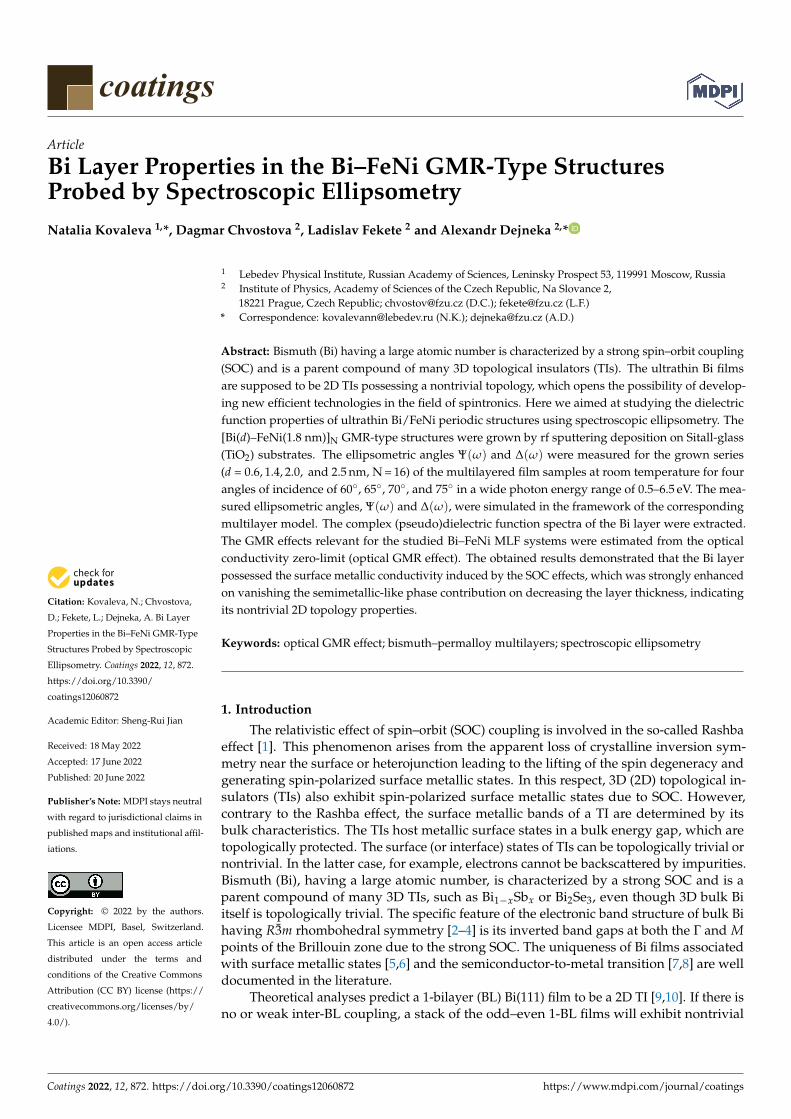
The retrieved 5 × 5 µm2 and 1 × 1µm2 AFM images of the Al2O3(2.1 nm)/[Bi(0.6, 1.4,2.0, 2.5 nm)–FeNi(1.8 nm)]N/Sitall multilayered films (where the given layer thicknessescorrespond to their nominal values) presented in Figure 1a–h show a discernible contrastbecause of the available surface height deviations. The surface roughness of the Sitall glass(TiO2) substrates was investigated by AFM in our earlier publication [17]. The height profileof the Sitall substrates (see Ref. [17], Figure 2a) demonstrated a height deviation within therange 1–3 nm characteristic of the relatively large 0.3–1 µm lateral scale, which characterizesthe Sitall substrate surface roughness. From the AFM measurements on the areas 5× 5 µm2
and 1 × 1 µm2 the root-mean square (RMS) surface roughness values were evaluated,which are presented in the caption to Figure 1. The corresponding RMS roughness valuesare notably higher for the Al2O3(2.1 nm)/[Bi(2.5 nm)–FeNi(1.8 nm)]16/Sitall MLF sample.The smaller-scale (1× 1µm2) images clearly exhibit a fine grainy-like structure of thesurface morphology, which seems to be characteristic for all studied film samples (seeFigure 1e–h). The typical grain size, of about 50 nm, is notably larger for the FeNi(1.8 nm)-BiMLF sample incorporating the 2.5 nm thick Bi layers, and, following the estimated RMSroughness values, the average grain size decreases to about 20 nm when decreasing theBi layer thickness to 1.4 nm. As one can see from the typical height profiles presented inFigure 1i,j, when decreasing the Bi layer thickness from 2.5 to about 0.6 nm, the surfacemorphology becomes highly irregular due to the formation of conglomerates of nanoislandsseparated by rather flat (relatively small roughness) areas of about 20 nm.
Coatings 2022, 12, 872 4 of 13
Figure 1. AFM images (a–d) 5 × 5 µm2 and (e–h) 1 × 1 µm2 of the Al2O3/(Bi–FeNi)16/Sitall MLFsamples, where the nominal Al2O3 and FeNi layer thicknesses are 2.1 and 1.8 nm and the nominalBi layer thicknesses are 0.6, 1.4, 2.0, and 2.5 nm, respectively. The estimated surface RMS roughnessvalues are in (a–d), 3.6, 3.0, 3.1, and 5.2 nm, and in (e–h), 3.2, 2.6, 2.7, and 5.3 nm, respectively.(i,j) The typical height profiles for the MLF samples with the nominal Bi layer thicknesses of 0.6 and2.5 nm, respectively.
3.2. Spectroscopic Ellipsometry Study of the Ultrathin Bi–FeNi Multilayer Film Samples
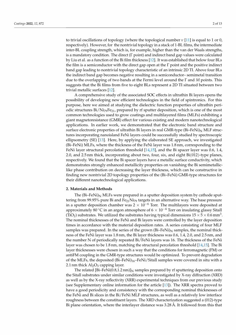
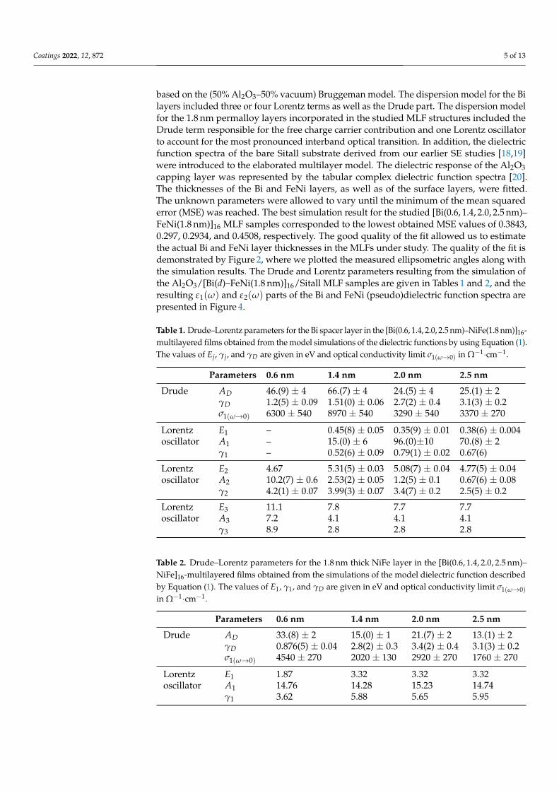
The ellipsometric angles Ψ(ω) and ∆(ω) were measured for the prepared Al2O3/(Bi–FeNi)16/Sitall MLF samples at the angles of incidence of 60, 65, 70, and 75. Figure 2demonstrates the ellipsometric angles Ψ(ω) and ∆(ω) recorded at 65 and 70. To modelthe contributions from free charge carriers and interband optical transitions, the complexdielectric function ε(ω) = ε1(ω) + iε2(ω) of the Bi and FeNi layers was interpreted interms of the Drude and Lorentz parts, respectively,
ε(E ≡ hω) = ε∞ −AD
E2 + iEγD+ ∑
j
AjγjEj
E2j − E2 − iEγj
, (1)
where ε∞ is the high-frequency dielectric constant, which takes into account the contribu-tion from the higher-energy interband transitions. The fitted Drude parameters were ADand the free charge carrier’s scattering rate γD. The fitted parameters of Lorentz bandswere Ej, γj, and Aj of the band maximum energy, the full width at half-maximum, and theε2 band height, respectively. The obtained ellipsometric angles Ψ(ω) and ∆(ω) measuredat different angles of incidence of 60, 65, 70, and 75 were fitted for each sample si-multaneously using J.A. Woollam VASE software [16] in the framework of the designedmultilayer model. The multilayer model for the studied Al2O3/(Bi–FeNi)/Sitall multilayerswas constructed as it is schematically presented in Figure 3, exactly so, as the layers weredeposited. In addition, we attempted to take into account the roughness properties of thesurface by using the conventional approach of effective medium approximation (EMA)
Coatings 2022, 12, 872 5 of 13
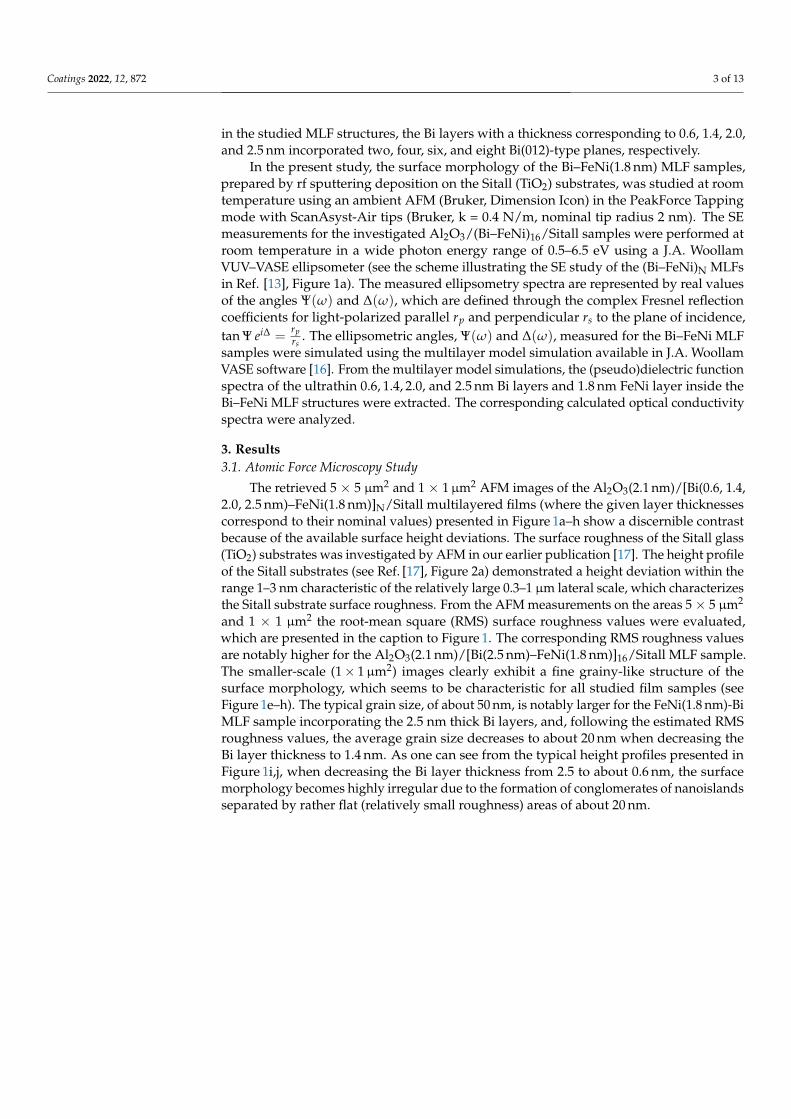
based on the (50% Al2O3–50% vacuum) Bruggeman model. The dispersion model for the Bilayers included three or four Lorentz terms as well as the Drude part. The dispersion modelfor the 1.8 nm permalloy layers incorporated in the studied MLF structures included theDrude term responsible for the free charge carrier contribution and one Lorentz oscillatorto account for the most pronounced interband optical transition. In addition, the dielectricfunction spectra of the bare Sitall substrate derived from our earlier SE studies [18,19]were introduced to the elaborated multilayer model. The dielectric response of the Al2O3capping layer was represented by the tabular complex dielectric function spectra [20].The thicknesses of the Bi and FeNi layers, as well as of the surface layers, were fitted.The unknown parameters were allowed to vary until the minimum of the mean squarederror (MSE) was reached. The best simulation result for the studied [Bi(0.6, 1.4, 2.0, 2.5 nm)–FeNi(1.8 nm)]16 MLF samples corresponded to the lowest obtained MSE values of 0.3843,0.297, 0.2934, and 0.4508, respectively. The good quality of the fit allowed us to estimatethe actual Bi and FeNi layer thicknesses in the MLFs under study. The quality of the fit isdemonstrated by Figure 2, where we plotted the measured ellipsometric angles along withthe simulation results. The Drude and Lorentz parameters resulting from the simulation ofthe Al2O3/[Bi(d)–FeNi(1.8 nm)]16/Sitall MLF samples are given in Tables 1 and 2, and theresulting ε1(ω) and ε2(ω) parts of the Bi and FeNi (pseudo)dielectric function spectra arepresented in Figure 4.
Table 1. Drude–Lorentz parameters for the Bi spacer layer in the [Bi(0.6, 1.4, 2.0, 2.5 nm)–NiFe(1.8 nm)]16-multilayered films obtained from the model simulations of the dielectric functions by using Equation (1).The values of Ej, γj, and γD are given in eV and optical conductivity limit σ1(ω→0) in Ω−1·cm−1.
Parameters 0.6 nm 1.4 nm 2.0 nm 2.5 nm
Drude AD 46.(9) ± 4 66.(7) ± 4 24.(5) ± 4 25.(1) ± 2γD 1.2(5) ± 0.09 1.51(0) ± 0.06 2.7(2) ± 0.4 3.1(3) ± 0.2σ1(ω→0) 6300 ± 540 8970 ± 540 3290 ± 540 3370 ± 270
Lorentz E1 – 0.45(8) ± 0.05 0.35(9) ± 0.01 0.38(6) ± 0.004oscillator A1 – 15.(0) ± 6 96.(0)±10 70.(8) ± 2
γ1 – 0.52(6) ± 0.09 0.79(1) ± 0.02 0.67(6)
Lorentz E2 4.67 5.31(5) ± 0.03 5.08(7) ± 0.04 4.77(5) ± 0.04oscillator A2 10.2(7) ± 0.6 2.53(2) ± 0.05 1.2(5) ± 0.1 0.67(6) ± 0.08
γ2 4.2(1) ± 0.07 3.99(3) ± 0.07 3.4(7) ± 0.2 2.5(5) ± 0.2
Lorentz E3 11.1 7.8 7.7 7.7oscillator A3 7.2 4.1 4.1 4.1
γ3 8.9 2.8 2.8 2.8
Table 2. Drude–Lorentz parameters for the 1.8 nm thick NiFe layer in the [Bi(0.6, 1.4, 2.0, 2.5 nm)–NiFe]16-multilayered films obtained from the simulations of the model dielectric function describedby Equation (1). The values of E1, γ1, and γD are given in eV and optical conductivity limit σ1(ω→0)in Ω−1·cm−1.
Parameters 0.6 nm 1.4 nm 2.0 nm 2.5 nm
Drude AD 33.(8) ± 2 15.(0) ± 1 21.(7) ± 2 13.(1) ± 2γD 0.876(5) ± 0.04 2.8(2) ± 0.3 3.4(2) ± 0.4 3.1(3) ± 0.2σ1(ω→0) 4540 ± 270 2020 ± 130 2920 ± 270 1760 ± 270
Lorentz E1 1.87 3.32 3.32 3.32oscillator A1 14.76 14.28 15.23 14.74
γ1 3.62 5.88 5.65 5.95
Coatings 2022, 12, 872 6 of 13
Figure 2. (a–d) Ellipsometric angles, Ψ(ω) and ∆(ω) (symbols), measured at the angles of incidenceof 65 and 70 for the Al2O3/[Bi(d)–NiFe(1.8 nm)]16/Sitall multilayered films where the Bi spacerlayer thicknesses d = 0.6, 1.4, 2.0, and 2.5 nm, respectively. The solid red, blue, green, and black curvesshow the corresponding simulation results for a 65 angle by the dielectric function model usingEquation (1).
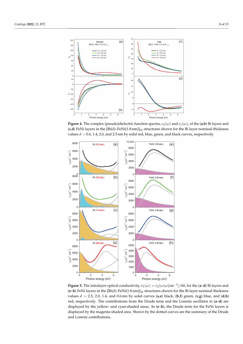
From Figure 4a,b one can see that the complex (pseudo)dielectric functions of the 0.6,1.4, 2.0, and 2.5 nm thick Bi spacers inside the investigated Bi–FeNi MLFs demonstratea metallic character. Moreover, the ε1(ω) function progressively decreases while the Bithickness decreases from 2.5 to 2.0 to 1.4 nm and the ε2(ω) increases at low photon energies,respectively. According to our simulation results, we expect that the best metallicityproperties are demonstrated by the Bi layer in the [Bi(1.4 nm)–NiFe(1.8 nm)]16 structure.At the same time, the complex (pseudo)dielectric functions of the thinnest 0.6 nm thickBi layer look somewhat different. Here, in addition to the low-energy metallic Druderesponse identified by the characteristic behavior of ε1(ω) and ε2(ω), the Lorentz bandaround 4–5 eV makes an essential contribution to the dielectric function response (thecorresponding Drude (AD and γD) and Lorentz (Aj, Ej, and γj) parameters are listed inTable 1). Next, being similar, the dielectric functions of the 1.8 nm thick permalloy layersin the [FeNi–Bi(1.4, 2.0, 2.5 nm)] MLFs are dominated by the ε2(ω) resonance and ε1(ω)
Coatings 2022, 12, 872 7 of 13
antiresonance features, indicating the predominant contribution from the Lorentz oscillatorpeaking at around 3 eV (see Figure 4c,d). An upturn evident in the ε2(ω) at low photonenergies indicates an additional Drude contribution, which is relatively less pronounced.Following our simulation results, we expect the advanced metallicity properties of the FeNilayer in the [Bi(0.6 nm)–NiFe(1.8 nm)]16 structure (see the corresponding Drude (AD andγD) and Lorentz (Aj, Ej, and γj) parameters listed in Table 2).
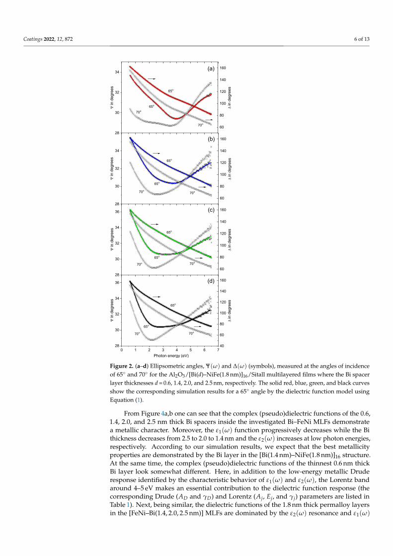
Figure 5a–d present the evolution of the Bi intralayer optical conductivity, σ1(ω) =ε2(ω)ω(cm−1)/60, upon decreasing the Bi spacer layer thickness in the [FeNi(1.8 nm)–Bi(2.5, 2.0, 1.4, 0.6 nm)]16 structures, and Figure 5e–h show the associated optical conduc-tivity spectra of the 1.8 nm FeNi permalloy layer. Here, the contributions from the Drudeand Lorentz oscillators following the multilayer model simulations using Equation (1)are evidently demonstrated. The presented optical conductivity spectra of the Bi andFeNi layers follow the main trends identified in their complex dielectric function spectrapresented in Figure 4.
(a)
(b)
( )
(d)
c
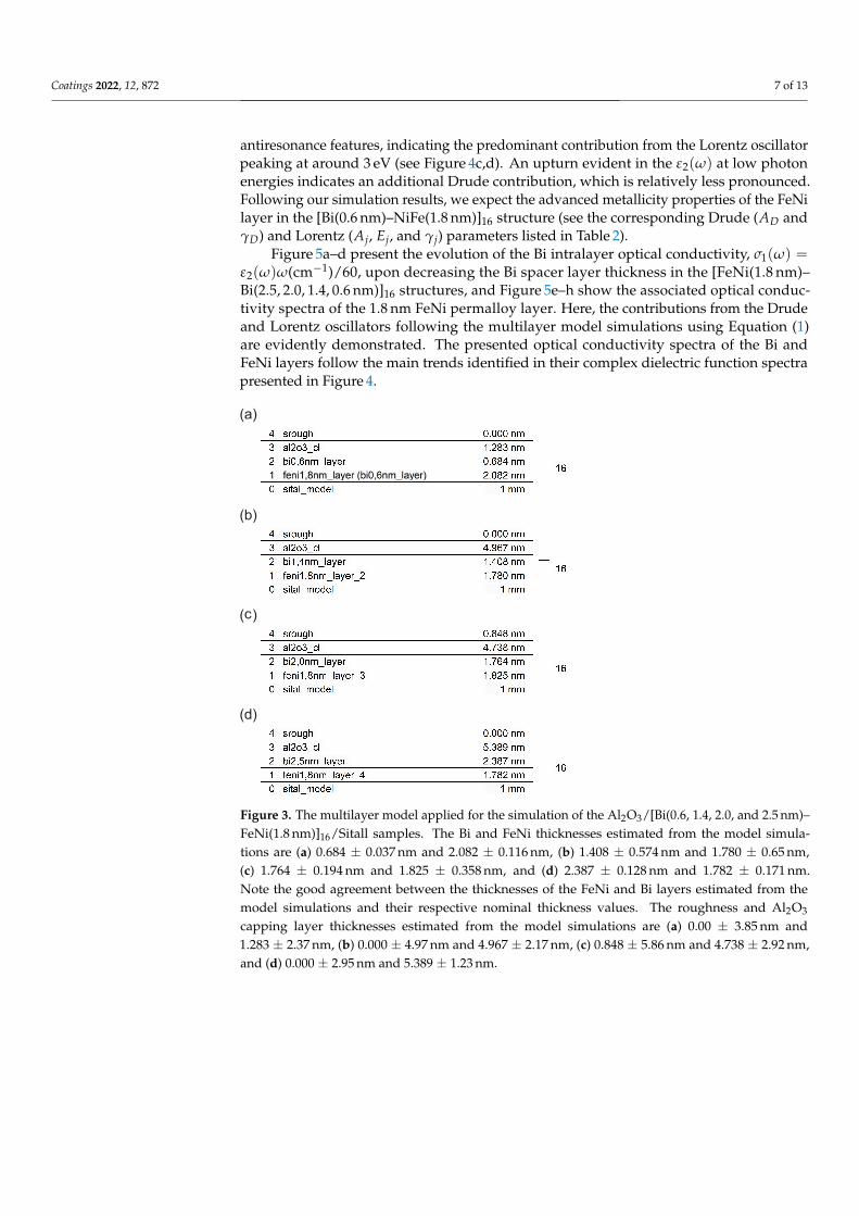
Figure 3. The multilayer model applied for the simulation of the Al2O3/[Bi(0.6, 1.4, 2.0, and 2.5 nm)–FeNi(1.8 nm)]16/Sitall samples. The Bi and FeNi thicknesses estimated from the model simula-tions are (a) 0.684 ± 0.037 nm and 2.082 ± 0.116 nm, (b) 1.408 ± 0.574 nm and 1.780 ± 0.65 nm,(c) 1.764 ± 0.194 nm and 1.825 ± 0.358 nm, and (d) 2.387 ± 0.128 nm and 1.782 ± 0.171 nm.Note the good agreement between the thicknesses of the FeNi and Bi layers estimated from themodel simulations and their respective nominal thickness values. The roughness and Al2O3
capping layer thicknesses estimated from the model simulations are (a) 0.00 ± 3.85 nm and1.283 ± 2.37 nm, (b) 0.000 ± 4.97 nm and 4.967 ± 2.17 nm, (c) 0.848 ± 5.86 nm and 4.738 ± 2.92 nm,and (d) 0.000 ± 2.95 nm and 5.389 ± 1.23 nm.
Coatings 2022, 12, 872 8 of 13
Figure 4. The complex (pseudo)dielectric function spectra, ε2(ω) and ε1(ω), of the (a,b) Bi layers and(c,d) FeNi layers in the [Bi(d)–FeNi(1.8 nm)]16 structures shown for the Bi layer nominal thicknessvalues d = 0.6, 1.4, 2.0, and 2.5 nm by solid red, blue, green, and black curves, respectively.
Figure 5. The intralayer optical conductivity, σ1(ω) = ε2(ω)ω[cm−1]/60, for the (a–d) Bi layers and(e–h) FeNi layers in the [Bi(d)–FeNi(1.8 nm)]16 structures shown for the Bi layer nominal thicknessvalues d = 2.5, 2.0, 1.4, and 0.6 nm by solid curves (a,e) black, (b,f) green, (c,g) blue, and (d,h)red, respectively. The contributions from the Drude term and the Lorentz oscillator in (a–d) aredisplayed by the yellow- and cyan-shaded areas. In (e–h), the Drude term for the FeNi layers isdisplayed by the magenta-shaded area. Shown by the dotted curves are the summary of the Drudeand Lorentz contributions.
Coatings 2022, 12, 872 9 of 13
4. Discussion
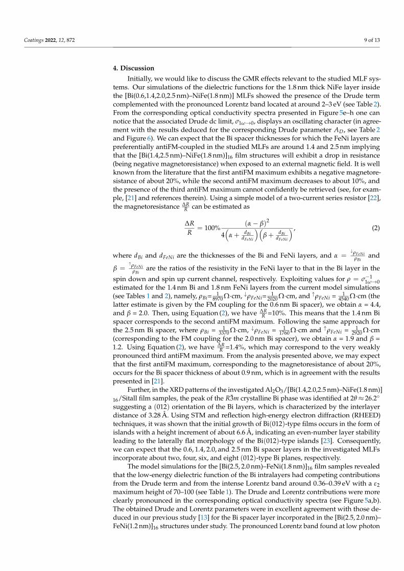
Initially, we would like to discuss the GMR effects relevant to the studied MLF sys-tems. Our simulations of the dielectric functions for the 1.8 nm thick NiFe layer insidethe [Bi(0.6,1.4,2.0,2.5 nm)–NiFe(1.8 nm)] MLFs showed the presence of the Drude termcomplemented with the pronounced Lorentz band located at around 2–3 eV (see Table 2).From the corresponding optical conductivity spectra presented in Figure 5e–h one cannotice that the associated Drude dc limit, σ1ω→0, displays an oscillating character (in agree-ment with the results deduced for the corresponding Drude parameter AD, see Table 2and Figure 6). We can expect that the Bi spacer thicknesses for which the FeNi layers arepreferentially antiFM-coupled in the studied MLFs are around 1.4 and 2.5 nm implyingthat the [Bi(1.4,2.5 nm)–NiFe(1.8 nm)]16 film structures will exhibit a drop in resistance(being negative magnetoresistance) when exposed to an external magnetic field. It is wellknown from the literature that the first antiFM maximum exhibits a negative magnetore-sistance of about 20%, while the second antiFM maximum decreases to about 10%, andthe presence of the third antiFM maximum cannot confidently be retrieved (see, for exam-ple, [21] and references therein). Using a simple model of a two-current series resistor [22],the magnetoresistance ∆R
R can be estimated as
∆RR
= 100%(α− β)2
4(
α + dBidFeNi
)(β + dBi
dFeNi
) , (2)
where dBi and dFeNi are the thicknesses of the Bi and FeNi layers, and α =↓ρFeNi
ρBiand
β =↑ρFeNi
ρBiare the ratios of the resistivity in the FeNi layer to that in the Bi layer in the
spin down and spin up current channel, respectively. Exploiting values for ρ = σ−11ω→0
estimated for the 1.4 nm Bi and 1.8 nm FeNi layers from the current model simulations(see Tables 1 and 2), namely, ρBi= 1
8970 Ω·cm, ↓ρFeNi= 12020 Ω·cm, and ↑ρFeNi = 1
4540 Ω·cm (thelatter estimate is given by the FM coupling for the 0.6 nm Bi spacer), we obtain α = 4.4,and β = 2.0. Then, using Equation (2), we have ∆R
R =10%. This means that the 1.4 nm Bispacer corresponds to the second antiFM maximum. Following the same approach forthe 2.5 nm Bi spacer, where ρBi = 1
3370 Ω·cm, ↓ρFeNi = 11760 Ω·cm and ↑ρFeNi = 1
2920 Ω·cm(corresponding to the FM coupling for the 2.0 nm Bi spacer), we obtain α = 1.9 and β =1.2. Using Equation (2), we have ∆R
R =1.4%, which may correspond to the very weaklypronounced third antiFM maximum. From the analysis presented above, we may expectthat the first antiFM maximum, corresponding to the magnetoresistance of about 20%,occurs for the Bi spacer thickness of about 0.9 nm, which is in agreement with the resultspresented in [21].
Further, in the XRD patterns of the investigated Al2O3/[Bi(1.4,2.0,2.5 nm)–NiFe(1.8 nm)]16/Sitall film samples, the peak of the R3m crystalline Bi phase was identified at 2θ≈ 26.2
suggesting a (012) orientation of the Bi layers, which is characterized by the interlayerdistance of 3.28 Å. Using STM and reflection high-energy electron diffraction (RHEED)techniques, it was shown that the initial growth of Bi(012)-type films occurs in the form ofislands with a height increment of about 6.6 Å, indicating an even-number layer stabilityleading to the laterally flat morphology of the Bi(012)-type islands [23]. Consequently,we can expect that the 0.6, 1.4, 2.0, and 2.5 nm Bi spacer layers in the investigated MLFsincorporate about two, four, six, and eight (012)-type Bi planes, respectively.
The model simulations for the [Bi(2.5, 2.0 nm)–FeNi(1.8 nm)]16 film samples revealedthat the low-energy dielectric function of the Bi intralayers had competing contributionsfrom the Drude term and from the intense Lorentz band around 0.36–0.39 eV with a ε2maximum height of 70–100 (see Table 1). The Drude and Lorentz contributions were moreclearly pronounced in the corresponding optical conductivity spectra (see Figure 5a,b).The obtained Drude and Lorentz parameters were in excellent agreement with those de-duced in our previous study [13] for the Bi spacer layer incorporated in the [Bi(2.5, 2.0 nm)–FeNi(1.2 nm)]16 structures under study. The pronounced Lorentz band found at low photon
Coatings 2022, 12, 872 10 of 13
energies for Bi single crystals (rhombohedral symmetry, space group R3m) [24,25] and bulkBi layers [26,27] is characteristic of the semimetallic-like electronic band structure due tothe contributions from the interband transitions near the Γ point, Γ+
6 – Γ−6 and Γ+45 – Γ−6 [2],
and near the T point, T−6 – T−45 [4]. The estimated values (see Table 1) of the Drude dclimit σ1ω→0 (2750–3830 Ω−1·cm−1) as well as the free charge carrier’s γD (2.3–3.3 eV) wereconsistent with those characteristic of the metallic surface states related to the RashbaSOC in Bi(111) films, σ1ω→0 = 2300 Ω−1·cm−1 and γD = 2.0 eV) [6]. Meanwhile, the modelsimulation for the [Bi(1.4 nm)–FeNi(1.8 nm)]16 structure indicated that for the 1.4 nm Bilayer, the Drude dc limit significantly increased to 8970 ± 540 Ω−1·cm−1, while the γDessentially decreased to 1.50± 0.06 eV. In this case, the Lorentz band was nearly suppressed.The associated found Drude parameters for the ultrathin Bi layer inside the [Bi(0.6 nm)–FeNi(1.8 nm)]16 structure were slightly different, namely, σ1ω→0 = 6300 ± 540 Ω−1·cm−1
and γD = 1.2 ± 0.1 eV, and the Lorentz band was clearly not present (see Figure 5c,d andTable 1).
Thus, we discovered that, on the one hand, the optical conductivity spectra of the2.0 and 2.5 nm thick Bi spacer layers in the (Bi–FeNi) MLFs incorporating eight and sixBi(012)-type monolayers, respectively, had contributions from the pronounced low-energyLorentz oscillator and from the free charge carrier Drude term (for details, see Figure 5a,band Table 1). Here, the presence of the low-energy Lorentz band points on the Bi semimetal-lic phase contribution and the parameters obtained for the Drude conductivity indicatethat its origin can be associated with the surface metallic states [6]. Therefore, the 2.0 and2.5 nm Bi layers can be associated with the semimetallic Bi phase sandwiched between twometallic layers on the top and bottom surfaces. On the other hand, the contribution fromthe intrinsic Lorentz band was strongly suppressed for the 1.4 and 0.6 nm layers, where theDrude conductivity displayed notably improved metallicity properties, as one can see fromthe optical conductivity spectra shown in Figure 5c,d (for details, see Table 1).
From the above discussion of the obtained results, we can conclude that the Bi layerconsisting of four Bi(012)-type monolayers represents a kind of crossover regarding thecontributions from the semimetallic Bi phase and/or surface metallic-like states. Here,we notice some similarity with the theory results presented for the ultrathin Bi(111) lay-ers by Liu et al. [12]. In their paper, it was established that below four Bi(111) BLs thefilm is a semiconductor with a direct gap open at the Γ point and a positive indirectband gap, leading to a nontrivial Z2 topology (ν = 1) characteristic of an intrinsic 2D TI.However, above four Bi(111) BLs, the indirect band gap becomes negative resulting in asemiconductor–semimetal transition, due to the overlapping of two bands at the Fermilevel around the Γ and M points. It was argued by Liu et al. [12] that the Bi layersconsisting of five to eight Bi(111) BLs represented a 2D TI placed between two “trivial”metallic surfaces [12]. This means that for the surface considered as an individual 2Dsystem, its Z2 number is trivial (ν = 0). The surface bands have no contribution to thenontrivial Z2 topology and, therefore, these trivial metallic surfaces are not robust and caneasily be removed by surface defects or impurities. We found [13] that the Bi layers in the[Bi(2.0, 2.5 nm)–FeNi(0.8 nm)] multilayers, incorporating the nanoisland permalloy layer,exhibited bulk-like semimetallic properties of the electronic band structure, although thesurface (Drude) metallic conductivity was absent there (see Ref. [13], Figure 4d). Indeed, astrong magnetic and spatial disorder induced by magnetic FeNi nanoislands, as well aslong-range many-body interactions between the magnetic moments of permalloy nanois-lands [17], may lead to a specific localization of free charge carriers [28]. However, the sur-face conductivity (or interface) states for the 1.4 nm layer in the Bi–FeNi(1.8 nm) multilayersmay be topologically nontrivial and, in this case, the electrons cannot be backscatteredby impurities. Here, the Drude dc limit was 8970 ± 540 Ω·cm−1 and the scattering rateγD = 1.5 ± 0.06 eV. We found that the 0.6 nm thick Bi layer exhibited somewhat differentDrude dc limit (6300 ± 540 Ω·cm−1) and γD (1.2 ± 0.1 eV), see Table 1 and Figure 6, whichcan be attributed to the discontinuous nanoisland structure of this layer.
Coatings 2022, 12, 872 11 of 13
Finally, we would like to note that it will be challenging to investigate the dc transportand superconductivity properties of the ultrathin Bi films possessing 2D TI surface statesfollowing the approach presented in [29], where the subkelvin superconductivity withoutany external stimuli was discovered in 3D TI Cd3As2 films [30,31].
Figure 6. (a,b) Parameters of the Drude term (AD and γD) for the Bi (filled symbols) and FeNi (emptysymbols) layers in the [Bi(0.6, 1.4, 2.0, 2.5 nm)–FeNi(1.8 nm)] MLF structures.
5. Conclusions
In summary, using wide-band (0.5–6.5 eV) spectroscopic ellipsometry, we studiedthe optical properties of the [Bi(0.6, 1.4, 2.0, 2.5 nm)–FeNi(1.8nm)]16 MLFs prepared by rfsputtering. The XRD analysis suggested that the 0.6, 1.4, 2.0, and 2.5 nm Bi layers in thestudied MLFs corresponded to about two, four, six, and eight Bi(012)-type monolayers,respectively. From the multilayer model simulations of the measured ellipsometric data, weextracted the Bi and FeNi layer dielectric functions. The dielectric function for the 2.0 and2.5 nm Bi spacer layers were represented by the Drude resonance due to the surface statesand the low-energy Lorentz band peaking at around 0.3–0.4 eV. The pronounced Lorentzband was characteristic of the semimetallic bulk-like Bi electronic zone structure due to thecontributions from the interband transitions near the Γ point. We discovered that the 2.0and 2.5 nm Bi spacer layers could be associated with the semimetallic Bi phase sandwichedbetween two trivial (where the topology number ν = 0) metallic layers on the top andbottom surfaces. The contribution from the low-photon-energy Lorentz band was stronglysuppressed for the 1.4 and 0.6 nm Bi layers, where the Drude conductivity displayednotably improved metallicity properties. This indicated that the Bi layer consisting of fourBi(012)-type monolayers represented a kind of crossover regarding the contributions fromthe semimetallic Bi phase and/or surface metallic-like states. Therefore, the properties ofBi layers below four monolayers may be associated with the nontrivial topology (wherethe topology number ν = 1) characteristic of an intrinsic 2D TI. We expect that the Bilayers having thickness of 0.9 nm will exhibit a maximal GMR effect of about 20% in the(Bi–FeNi) MLFs, where the Drude dc limit is about 8970 ± 540 Ω·cm−1. These states maybe protected from backscattering, which makes them promising in spintronic devices andquantum computing.
Coatings 2022, 12, 872 12 of 13
Author Contributions: Conceptualization, N.K. and A.D.; methodology, D.C. and L.F.; validation,N.K. and A.D.; investigation, D.C. and N.K.; data curation, D.C. and N.K.; writing—original draftpreparation, N.K.; writing—review and editing, N.K. and A.D.; visualization, N.K. and L.F.; supervi-sion, N.K. and A.D.; project administration, A.D.; funding acquisition, A.D. All authors have readand agreed to the published version of the manuscript.
Funding: This work was supported in part by the European Structural and Investment Funds and theCzech Ministry of Education, Youth, and Sports (Project No. SOLID21, Cz 02.1.01/0.0/0.0/16−019/0000760).
Institutional Review Board Statement: Not applicable.
Informed Consent Statement: Not applicable.
Data Availability Statement: Not applicable.
Acknowledgments: We thank F.A. Pudonin for providing us with the Bi/FeNi multilayer filmsamples and O. Pacherova for their XRD analysis. We thank A. Muratov for participation in thespectroscopic ellipsometry measurements.
Conflicts of Interest: The authors declare no conflict of interest.
Sample Availability: Samples of the Bi/FeNi multilayer films are available from the P.N. LebedevPhysical Institute, Moscow, Russia.
AbbreviationsThe following abbreviations are used in this manuscript:
GMR Giant magnetoresistanceSOC Spin–orbit couplingTI Topological insulatorMLF Multilayered filmSE Spectroscopic ellipsometryAFM Atomic force microscopyFM FerromagneticXRD X-ray diffractionXRR X-ray reflectivity
References1. Bychkov, Y.A.; Rashba, E.I. Properties of a 2D electron gas with lifted spectral degeneracy. JETP Lett. 1984, 39, 78–81.2. Golin, S. Band Structure of Bismuth: Pseudopotential Approach. Phys. Rev. B 1968, 166, 643–651. [CrossRef]3. Gonze, X.; Michenaud, J.-P.; Vigneron, J.-P. First-principles study of As, Sb, and Bi electronic properties. Phys. Rev. B 1990, 41,
11827–11836. [CrossRef] [PubMed]4. Liu, Y.; Allen, R.E. Electronic structure of the semimetals Bi and Sb. Phys. Rev. B 1995, 52, 1566–1577. [CrossRef] [PubMed]5. Hofmann, P. The surfaces of bismuth: Structural and electronic properties. Prog. Surf. Sci. 2006, 81, 191–245. [CrossRef]6. Yokota, Y.; Takeda, J.; Dang, C.; Han, G.; McCarthy, D.N.; Nagao, T.; Hishita, S.; Kitajima, K.; Katayama, I. Surface metallic states
in ultrathin Bi(001) films studied with terahertz time-domain spectroscopy. Appl. Phys. Lett. 2012, 100, 251605. [CrossRef]7. Hoffman, C.A.; Meyer, J.R.; Bartoli, F.J. Semimetal-to-semiconductor transition in Bismuth thin films. Phys. Rev. B 1993, 48,
11431–11434. [CrossRef]8. Koroteev, Y.M.; Bihlmayer, G.; Chulkov, E.V.; Blugel, S. First-principles investigation of structural and electronic properties of
ultrathin Bi films. Phys. Rev. B 2008, 77, 045428–. [CrossRef]9. Wada, M.; Murakami, S.; Freimuth, F.; Bihlmayer, G. Localized edge states in two-dimensional topological insulators: Ultrathin Bi
films. Phys. Rev. B 2011, 83, 121310(R). [CrossRef]10. Murakami, S. Quantum Spin Hall Effect and Enhanced Magnetic Response by Spin-Orbit Coupling. Phys. Rev. Lett. 2006,
97, 236805. [CrossRef]11. Fu, L.; Kane, C.L.; Mele, E.J. Topological Insulators in Three Dimensions. Phys. Rev. Lett. 2007, 98, 106803. [CrossRef] [PubMed]12. Liu, Z.; Liu, C.-X.; Wu, Y.-S.; Duan, W.-H.; Liu, F.; Wu, J. Stable nontrivial Z2 topology in ultrathin Bi(111) films: A first principles
study. Phys. Rev. Lett. 2011, 107, 136805. [CrossRef] [PubMed]13. Kovaleva, N.N.; Chvostova, D.; Pacherova O.; Muratov A.V.; Fekete L.; Sherstnev I.A.; Kugel K.I.; Pudonin F.A.; Dejneka A.
Bismuth layer properties in the ultrathin Bi–FeNi multilayer films probed by spectroscopic ellipsometry. Appl. Phys. Lett. 2021,119, 183101. [CrossRef]
14. Sherstnev, I.A. Electronic Transport and Magnetic Structure of Nanoisland Ferromagnetic Systems. Ph.D. Thesis, P.N. LebedevPhysical Institute, Moscow, Russia, 2014.
Coatings 2022, 12, 872 13 of 13
15. Boltaev, A.P.; Pudonin, F.A.; Shertnev, I.A.; Egorov, D.A. Detection of the metal-insulator transition in disordered systems ofmagnetic nanoislands. JETP 2017, 125, 465–468. [CrossRef]
16. Woollam, J.A. VASE Spectroscopic Ellipsometry Data Analysis Software; J.A. Woollam, Co.: Lincoln, NE, USA, 2010.17. Stupakov, A.; Bagdinov, A.V.; Prokhorov, V.V.; Bagdinova, A.N.; Demikhov, E.I.; Dejneka, A.; Kugel, K.I.; Gorbatsevich, A.A.;
Pudonin, F.A.; Kovaleva, N.N. Out-of-plane and in-plane magnetization behaviour of dipolar interacting FeNi nanoislandsaround the percolation threshold. J. Nanomater. 2016, 3190260. http://dx.doi.org/10.1155/2016/3190260. [CrossRef]
18. Kovaleva, N.N.; Chvostova, D.; Bagdinov, A.V.; Petrova M.G.; Demikhov E.I.; Pudonin F.A.; Dejneka A. Interplay of electroniccorrelation and localization in disordered β-tantalum films: Evidence from dc transport and spectroscopic ellipsometry study.Appl. Phys. Lett. 2015, 106, 051907. [CrossRef]
19. Kovaleva, N.; Chvostova, D.; Dejneka, A. Localization phenomena in disordered tantalum films. Metals 2017, 7, 257. [CrossRef]20. Palik, E.D. Handbook of Optical Constants of Solids; Elsevier Science: San Diego, CA, USA, 1991.21. Hütten, A.; Mrozek, S.; Heitmann, S.; Hempel, T.; Brückl H.; Reiss, G. Evolution of the GMR-Effect Amplitude in Copper-
Permalloy-Multilayered Thin Films. Acta Mater. 1999, 47, 4245–4252. [CrossRef]22. Mathon, J. Exchange Interactions and Giant Magnetoresistance in Magnetic Multilayers. Contemp. Phys. 1991, 32, 143–156.
[CrossRef]23. Nagao, T.; Sadowski, J.T.; Saito, M.; Yaginuma, S.; Fujikawa, Y.; Kogure, T.; Ohno, T.; Hasegawa, S.; Sakurai, T. Nanofilm allotrope
and phase transformation of ultrathin Bi film on Si(111)-7 × 7. Phys. Rev. Lett. 2004, 93, 105501. [CrossRef]24. Wang, P.Y.; Jain, A.L. Modulated Piezoreflectance in Bismuth. Phys. Rev. B 1970, 2, 2978–2983. [CrossRef]25. Lenham, A.P.; Treherne, D.M.; Metcalfe, R.J. Optical Properties of Antimony and Bismuth Crystals. J. Opt. Soc. Am. 1965, 55,
1072–1074. [CrossRef]26. Hunderi, O. Optical properties of crystalline and amorphous bismuth films. J. Phys. F 1975, 5, 2214–2225. [CrossRef]27. Toudert, J.; Serna, R. Interband transitions in semi-metals, semiconductors, and topological insulators: A new driving force for
plasmonics and nanophotonics [Invited]. Opt. Mater. Express 2017, 7, 2299–2325. [CrossRef]28. Kovaleva, N.N.; Kusmartsev, F.V.; Mekhiya, A.B.; Trunkin, I.N.; Chvostova, D.; Davydov, A.B.; Oveshnikov, L.N.; Pacherova, O.;
Sherstnev, I.A.; Kusmartseva, A.; et al. Control of Mooij correlations at the nanoscale in the disordered metallic Ta-nanoislandFeNi multilayers. Sci. Rep. 2020, 10, 21172. [CrossRef] [PubMed]
29. Suslov, A.V.; Davydov, A.B.; Oveshnikov, L.N.; Morgun, L.A.; Kugel, K.I.; Zakhvalinskii, V.S.; Pilyuk, E.A.; Kochura, A.V.;Kuzmenko, A.P.; Pudalov, V.M.; et al. Observation of subkelvin superconductivity in Cd3As2 thin films. Phys. Rev. B 2019,99, 094512. [CrossRef]
30. Kochura, A.V.; Zakhvalinskii, V.S.; Htet, A.Z.; Ril’, A.I.; Pilyuk, E.A.; Kuz’menko, A.P.; Aronzon, B.A.; Marenkin, S.F. Growth ofthin cadmium arsenide films by magnetron sputtering and their structure. Inorg. Mater. 2019, 55, 879–886. [CrossRef]
31. Kovaleva, N.; Chvostova, D.; Fekete, L.; Muratov, A. Morphology and Optical Properties of Thin Cd3As2 Films of a DiracSemimetal Compound. Metals 2020, 10, 1398. [CrossRef]
Related Documents