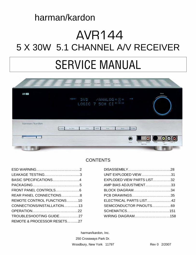
harman/kardon AVR144 5 X 30W 5.1 CHANNEL A/V RECEIVER SERVICE MANUAL CONTENTS ESD WARNING……………………………….2 LEAKAGE TESTING……………….…..…....3 BASIC SPECIFICATIONS…………………..4 PACKAGING…………………………….……5 FRONT PANEL CONTROLS………..…..…..6 REAR PANEL CONNECTIONS………….…8 REMOTE CONTROL FUNCTIONS……….10 CONNECTIONS/INSTALLATION………....13 OPERATION………………………...………22 TROUBLESHOOTING GUIDE…...……..…27 REMOTE & PROCESSOR RESETS……....27 DISASSEMBLY……………………………….28 UNIT EXPLODED VIEW…………..…….…..31 EXPLODED VIEW PARTS LIST……………32 AMP BIAS ADJUSTMENT……………….…33 BLOCK DIAGRAM…………………………..34 PCB DRAWINGS……………………………35 ELECTRICAL PARTS LIST………..….……42 SEMICONDUCTOR PINOUTS…….………69 SCHEMATICS………………………………151 WIRING DIAGRAM…………………………158 harman/kardon, Inc. 250 Crossways Park Dr. Woodbury, New York 11797 Rev 0 2/2007

Welcome message from author
This document is posted to help you gain knowledge. Please leave a comment to let me know what you think about it! Share it to your friends and learn new things together.
Transcript
harman/kardon
AVR144 5 X 30W 5.1 CHANNEL A/V RECEIVER
SERVICE MANUAL
CONTENTS
ESD WARNING……………………………….2 LEAKAGE TESTING……………….…..…....3 BASIC SPECIFICATIONS…………………..4 PACKAGING…………………………….……5 FRONT PANEL CONTROLS………..…..…..6 REAR PANEL CONNECTIONS………….…8 REMOTE CONTROL FUNCTIONS……….10 CONNECTIONS/INSTALLATION………....13 OPERATION………………………...………22 TROUBLESHOOTING GUIDE…...……..…27 REMOTE & PROCESSOR RESETS……....27
DISASSEMBLY……………………………….28 UNIT EXPLODED VIEW…………..…….…..31 EXPLODED VIEW PARTS LIST……………32 AMP BIAS ADJUSTMENT……………….…33 BLOCK DIAGRAM…………………………..34 PCB DRAWINGS……………………………35 ELECTRICAL PARTS LIST………..….……42 SEMICONDUCTOR PINOUTS…….………69 SCHEMATICS………………………………151 WIRING DIAGRAM…………………………158
harman/kardon, Inc.
250 Crossways Park Dr.
Woodbury, New York 11797 Rev 0 2/2007
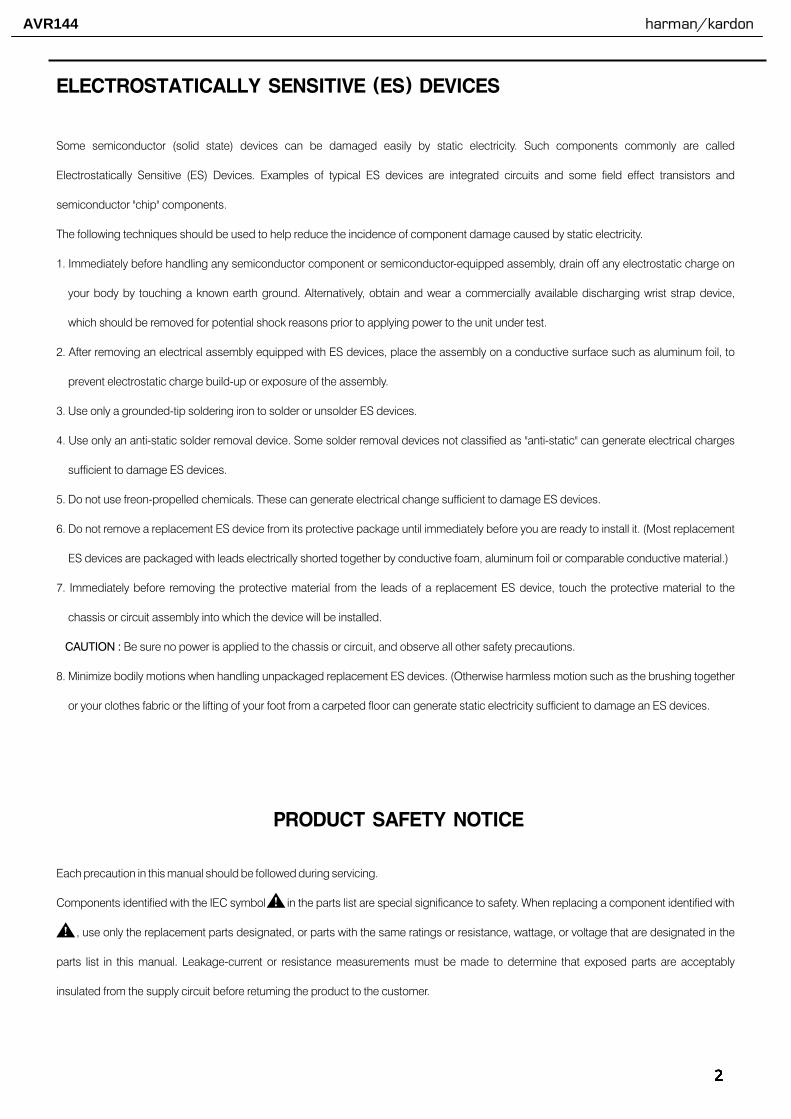
Each precaution in this manual should be followed during servicing.
Components identified with the IEC symbol in the parts list are special significance to safety. When replacing a component identified with
, use only the replacement parts designated, or parts with the same ratings or resistance, wattage, or voltage that are designated in the
parts list in this manual. Leakage-current or resistance measurements must be made to determine that exposed parts are acceptably
insulated from the supply circuit before retuming the product to the customer.
Some semiconductor (solid state) devices can be damaged easily by static electricity. Such components commonly are called
Electrostatically Sensitive (ES) Devices. Examples of typical ES devices are integrated circuits and some field effect transistors and
semiconductor "chip" components.
The following techniques should be used to help reduce the incidence of component damage caused by static electricity.
1. Immediately before handling any semiconductor component or semiconductor-equipped assembly, drain off any electrostatic charge on
your body by touching a known earth ground. Alternatively, obtain and wear a commercially available discharging wrist strap device,
which should be removed for potential shock reasons prior to applying power to the unit under test.
2. After removing an electrical assembly equipped with ES devices, place the assembly on a conductive surface such as aluminum foil, to
prevent electrostatic charge build-up or exposure of the assembly.
3. Use only a grounded-tip soldering iron to solder or unsolder ES devices.
4. Use only an anti-static solder removal device. Some solder removal devices not classified as "anti-static" can generate electrical charges
sufficient to damage ES devices.
5. Do not use freon-propelled chemicals. These can generate electrical change sufficient to damage ES devices.
6. Do not remove a replacement ES device from its protective package until immediately before you are ready to install it. (Most replacement
ES devices are packaged with leads electrically shorted together by conductive foam, aluminum foil or comparable conductive material.)
7. Immediately before removing the protective material from the leads of a replacement ES device, touch the protective material to the
chassis or circuit assembly into which the device will be installed.
Be sure no power is applied to the chassis or circuit, and observe all other safety precautions.
8. Minimize bodily motions when handling unpackaged replacement ES devices. (Otherwise harmless motion such as the brushing together
or your clothes fabric or the lifting of your foot from a carpeted floor can generate static electricity sufficient to damage an ES devices.
CAUTION :
AVR144 harman/kardon

SAFETY PRECAUTIONS
The following check should be performed for the continuedprotection of the customer and service technician.
LEAKAGE CURRENT CHECK
Measure leakage current to a known earth ground (waterpipe, conduit, etc.) by connecting a leakage current testerbetween the earth ground and all exposed metal parts of theappliance (input/output terminals, screwheads, metaloverlays, control shaft, etc.). Plug the AC line cord of theappliance directly into a 120V AC 60Hz outlet and turn theAC power switch on. Any current measured must not exceedo.5mA.
ANY MEASUREMENTS NOT WITHIN THE LIMITSOUTLINED ABOVE ARE INDICATIVE OF APOTENTIAL SHOCK HAZARD AND MUST BECORRECTED BEFORE RETURNING THE APPLIANCETO THE CUSTOMER.
Deviceundertest
Test allexposed metalsurfaces
Also test withplug reversed(Using AC adapterplug as required)
AC Leakage Test
Leakagecurrenttester
Reading shouldnot be above0.5mA
Earthground
3
AVR144 harman/kardon
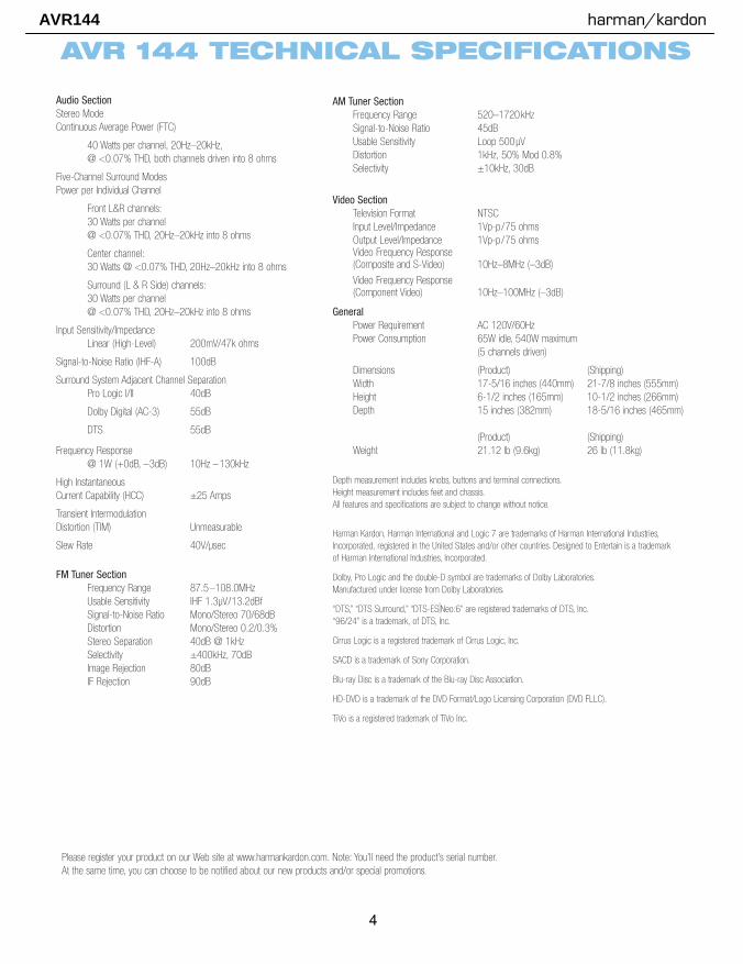
AVR 144 TECHNICAL SPECIFICATIONS
Audio SectionStereo Mode Continuous Average Power (FTC)
40 Watts per channel, 20Hz–20kHz,@ <0.07% THD, both channels driven into 8 ohms
Five-Channel Surround Modes Power per Individual Channel
Front L&R channels:30 Watts per channel@ <0.07% THD, 20Hz–20kHz into 8 ohms
Center channel:30 Watts @ <0.07% THD, 20Hz–20kHz into 8 ohms
Surround (L & R Side) channels:30 Watts per channel@ <0.07% THD, 20Hz–20kHz into 8 ohms
Input Sensitivity/ImpedanceLinear (High-Level) 200mV/47k ohms
Signal-to-Noise Ratio (IHF-A) 100dB
Surround System Adjacent Channel SeparationPro Logic I/II 40dB
Dolby Digital (AC-3) 55dB
DTS 55dB
Frequency Response @ 1W (+0dB, –3dB) 10Hz –130kHz
High Instantaneous Current Capability (HCC) ±25 Amps
Transient Intermodulation Distortion (TIM) Unmeasurable
Slew Rate 40V/μsec
FM Tuner SectionFrequency Range 87.5–108.0MHzUsable Sensitivity IHF 1.3μV/13.2dBfSignal-to-Noise Ratio Mono/Stereo 70/68dBDistortion Mono/Stereo 0.2/0.3%Stereo Separation 40dB @ 1kHzSelectivity ±400kHz, 70dBImage Rejection 80dBIF Rejection 90dB
AM Tuner SectionFrequency Range 520–1720kHzSignal-to-Noise Ratio 45dBUsable Sensitivity Loop 500μVDistortion 1kHz, 50% Mod 0.8%Selectivity ±10kHz, 30dB
Video SectionTelevision Format NTSCInput Level/Impedance 1Vp-p/75 ohmsOutput Level/Impedance 1Vp-p/75 ohmsVideo Frequency Response (Composite and S-Video) 10Hz–8MHz (–3dB)
Video Frequency Response (Component Video) 10Hz–100MHz (–3dB)
GeneralPower Requirement AC 120V/60HzPower Consumption 65W idle, 540W maximum
(5 channels driven)
Dimensions (Product) (Shipping)Width 17-5/16 inches (440mm) 21-7/8 inches (555mm) Height 6-1/2 inches (165mm) 10-1/2 inches (266mm) Depth 15 inches (382mm) 18-5/16 inches (465mm)
(Product) (Shipping)Weight 21.12 lb (9.6kg) 26 lb (11.8kg)
Depth measurement includes knobs, buttons and terminal connections.Height measurement includes feet and chassis.All features and specifications are subject to change without notice.
Harman Kardon, Harman International and Logic 7 are trademarks of Harman International Industries,Incorporated, registered in the United States and/or other countries. Designed to Entertain is a trademark of Harman International Industries, Incorporated.
Dolby, Pro Logic and the double-D symbol are trademarks of Dolby Laboratories.Manufactured under license from Dolby Laboratories.
“DTS,” “DTS Surround,” “DTS-ESINeo:6” are registered trademarks of DTS, Inc.“96/24” is a trademark, of DTS, Inc.
Cirrus Logic is a registered trademark of Cirrus Logic, Inc.
SACD is a trademark of Sony Corporation.
Blu-ray Disc is a trademark of the Blu-ray Disc Association.
HD-DVD is a trademark of the DVD Format/Logo Licensing Corporation (DVD FLLC).
TiVo is a registered trademark of TiVo Inc.
Please register your product on our Web site at www.harmankardon.com. Note: You’ll need the product’s serial number.At the same time, you can choose to be notified about our new products and/or special promotions.
HKP1482AVR144-om 9/7/06 3:12 PM Page 45
4
AVR144 harman/kardon

POLY BAG
NO DESCRIPTION PARTS NO. Q,ty
1
2
3
4
5
6
7
1
1
POLY BAG
MANUAL ASS'Y
BOX,OUT CARTON
4
5
1
2
DESCRIPTIONNO
CPS4A564
CPG1A820S
1
1
1
Q,tyPARTS NO.
CPS4A565SNOW,PAD(R)3 1
1. Instruction manual ass'y - Accessories 2. Package Drawing
SHEET GUIDE(QUICK START GUIDE)
STAPLE
8 CQE1A305Z
3
1
1
MANUAL ASS'Y1
SNOW PAD (R)3
BOX ,OUT CARTON5
SET4
SNOW PAD (L)2
CARTAVR144
CSA1A027Z
REMOCON TRANSMITTER ASS'Y
AM LOOP ANTENNA
BATTERY
1
1
3
CARD WARRANTY CQE1A172X 1
SNOW,PAD(L)
AVR144
1
INSTRUCTION MANUAL
FM 1 POL ANT(UL)
CQX1A1153Z
CSA1A019Z 1
1
CARD WARRANTY
SHEET GUIDE
2
BATTERY ASS'Y
4
REMOCONTRANSMITTER ASS'Y
87
3
AM LOOP ANTENNA ASS'Y
MANUAL INSTRUCTION
5
FM 1 POLE ANT(UL)
6
STAPLE
9
SHEET,FRONT COVER
COVER B
COVER A
BAG,POLY
PAD, COVER
CQE1A219Z
CGR1A332M7H43
CPS1A676
CGR1A331M7H43
11
1
1
1
1
10 CGRAVR130ZA 1
5
4
3
2
1
COVER ASS'Y
10
11
IMAGE BROCHURES11 1
IMAGE BROCHURES
9
AVR144 AVR 144
DOOR KIT
5
AVR144 harman/kardon

8
Main Power Switch: This is a mechanical switch that turns thepower supply on or off. It is usually left pressed in (On position) at alltimes, and cannot be turned on using the remote control.
Standby/On Switch: This is an electrical switch that turns thereceiver on for playback, or leaves it in standby mode for quick turn-onusing this switch or the remote control.
Power Indicator: This LED has three possible modes. When mainpower is turned off, the LED is dark and the receiver won’t respond toany button presses. When main power is turned on, but before theStandby/On Switch is used, the LED turns amber to indicate that thereceiver is in Standby mode and ready to be turned on. When thereceiver is turned on, the LED turns blue.
Source Select: Press this button to select a source device, which isa component where a playback signal originates, e.g., DVD, CD, cableTV, satellite or HDTV tuner.
Source Indicators: The name of the current source input lights up.The indicated input changes each time the Source Select Button ispressed.
Volume Knob: Turn this knob to raise or lower the volume, which willbe shown in decibels (dB) in the Message Display.
Message Display: Various messages appear in this two-line displayin response to commands. When the on-screen display menu system(OSD) is in use, the message OSD ON will appear to remind you tocheck the video display.
Tuner Band: Press this button to select the tuner as the source, or toswitch between the AM and FM bands.
Tuning: Press either side of this button to tune a radio station.
Tuning Mode: This button toggles between manual (one frequencystep at a time) and automatic (seeks frequencies with acceptable signalstrength) tuning mode. It also toggles between stereo and mono modeswhen an FM station is tuned.
Preset Stations: Press this button to select a preset radio station.
Headphone Jack: Plug a 1/4" headphone plug into this jack for private listening.
Surround Mode: Press this button to select a type of surroundsound (e.g., multichannel) mode. Choose from the Dolby modes, DTSmodes, Logic 7 modes, DSP modes or Stereo modes.
Surround Select: After you have selected the desired type of sur-round mode, press this button to select a specific variant of that type of mode.
Surround Mode Indicators: One or more of these icons may lightup as you select different surround modes. The Message Display alsoindicates the surround mode.
Analog Audio, Video and Digital Audio Inputs: Connect asource component that will only be used temporarily to these jacks,such as a camera or game console. Remember to select only one typeof audio and one type of video connection.
Speaker/Channel Input Indicators: The box icons indicatewhich speaker positions you have configured, and the size (frequencyrange) of each speaker. When a digital audio input is used, letters willlight inside the boxes to indicate which channels are present in theincoming signal.
FRONT-PANEL CONTROLS
HKP1482AVR144-om 9/7/06 3:10 PM Page 8
6
AVR144 harman/kardon

SurroundMode
Tuning Preset Stations
SurroundSelect
Tuner Band Tuning Mode
SourceSelect
HeadphoneJack
DigitalAudio Inputs
Video Inputs
Analog AudioInputs
PowerIndicator
Main PowerSwitch
Standby/OnSwitch
Volume
SourceIndicatorsMessage Display
Surround Mode Indicators Speaker/ChannelInput Indicators
NOTE: To make it easier to follow the instructions throughout the manual that refer to this illustration, a copy of this page may be downloaded from the Product Support section atwww.harmankardon.com.
HKP1482AVR144-om 9/7/06 3:10 PM Page 9
7
AVR144 harman/kardon

10
REAR-PANEL CONNECTIONS
AM and FM Antenna Terminals: Connect the included AM andFM antennas to their respective terminals for radio reception.
Front, Center and Surround Speaker Outputs: Use two-conductor speaker wire to connect each set of terminals to the correctspeaker. Remember to observe the correct polarity (positive and negativeconnections). Always connect the positive lead to the colored terminalon the receiver and the red terminal on the speaker. Connect the negativelead to the black terminal on both the receiver and the speaker. See theConnections section for more information on connecting your speakers.
Subwoofer Output: If you have a powered subwoofer, connect it tothis jack.
Video 1, Video 2 and DVD Audio/Video Inputs: These jacksmay be used to connect your video-capable source components (e.g.,VCR, DVD player, cable TV box) to the receiver. Remember to use onlyone type of video connection for each source. See the Connectionssection for more information on audio and video connection options foreach source component.
Video 1 Audio/Video Outputs: These jacks may be used to con-nect your VCR or another recorder.
Composite and S-Video Monitor Outputs: If some of yoursources use composite or S-video connections, then you will need toconnect one or both of these monitor outputs to the correspondinginputs on your television or video display in order to view the sources.
CD and Tape Audio Inputs: These jacks may be used to connectyour audio-only source components (e.g., CD player, tape deck). Do notconnect a turntable to these jacks unless you are using the turntablewith a phono preamp.
Tape Outputs: These jacks may be used to connect your CDR oranother audio-only recorder.
Coaxial and Optical Digital Audio Inputs: If your source has a compatible digital audio output, connect it to one of these jacks forimproved audio performance. Remember to use only one type of digitalaudio connection for each source.
6-Channel Inputs: Connect the analog audio outputs of a DVD-Audio, SACD™, Blu-ray Disc™ or HD-DVD™ player (or any other externaldecoder) to these jacks to enjoy these proprietary formats.
Component Video Inputs: If both your video source (e.g., DVDplayer or HDTV tuner) and your television or video display have analogcomponent video (Y/Pb/Pr) capability, then you may connect the com-ponent video outputs of your source to one of the two component videoinputs. Do not make any other video connections to that source.
Component Video Monitor Outputs: If you are using one orboth of the Component Video Inputs and your television or video displayis component-video-capable, you may connect these jacks to the corre-sponding inputs on your video display. You will also need to connect thecomposite and/or S-video monitor outputs to your video display if someof your sources use those types of video connections and to view theon-screen menus.
AC Power Cord: After you have made all other connections, plug theAC power cord into an unswitched outlet.
HKP1482AVR144-om 9/7/06 3:10 PM Page 10
8
AVR144 harman/kardon

FM Antenna
AM Antenna
Video 2A/VInputs
Video 1A/VOutputs
Video 1A/VInputs
VideoMonitorOutputs
DVD A/V Inputs
Component VideoInputs (1 & 2)
Component VideoMonitor Outputs
AC Power Cord
Coaxial DigitalAudio Inputs(1 & 2)
SubwooferOutput
Front SpeakerOutputs
SurroundSpeakerOutputs
6-ChannelInputs
CenterSpeakerOutputs
Optical DigitalAudio Inputs (1 & 2)
CDInputs
TapeOutputs
TapeInputs
NOTE: To make it easier to follow the instructions throughout the manual that refer to this illustration, a copy of this page may be downloaded from the Product Support section atwww.harmankardon.com.
HKP1482AVR144-om 9/7/06 3:10 PM Page 11
9
AVR144 harman/kardon
12
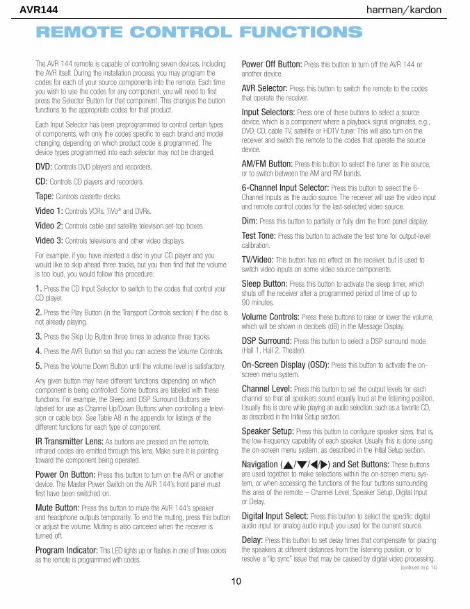
The AVR 144 remote is capable of controlling seven devices, includingthe AVR itself. During the installation process, you may program thecodes for each of your source components into the remote. Each timeyou wish to use the codes for any component, you will need to firstpress the Selector Button for that component. This changes the buttonfunctions to the appropriate codes for that product.
Each Input Selector has been preprogrammed to control certain types of components, with only the codes specific to each brand and modelchanging, depending on which product code is programmed. Thedevice types programmed into each selector may not be changed.
DVD: Controls DVD players and recorders.
CD: Controls CD players and recorders.
Tape: Controls cassette decks.
Video 1: Controls VCRs, TiVo® and DVRs.
Video 2: Controls cable and satellite television set-top boxes.
Video 3: Controls televisions and other video displays.
For example, if you have inserted a disc in your CD player and youwould like to skip ahead three tracks, but you then find that the volumeis too loud, you would follow this procedure:
1. Press the CD Input Selector to switch to the codes that control yourCD player.
2. Press the Play Button (in the Transport Controls section) if the disc isnot already playing.
3. Press the Skip Up Button three times to advance three tracks.
4. Press the AVR Button so that you can access the Volume Controls.
5. Press the Volume Down Button until the volume level is satisfactory.
Any given button may have different functions, depending on whichcomponent is being controlled. Some buttons are labeled with thesefunctions. For example, the Sleep and DSP Surround Buttons arelabeled for use as Channel Up/Down Buttons when controlling a televi-sion or cable box. See Table A8 in the appendix for listings of the different functions for each type of component.
IR Transmitter Lens: As buttons are pressed on the remote,infrared codes are emitted through this lens. Make sure it is pointingtoward the component being operated.
Power On Button: Press this button to turn on the AVR or anotherdevice. The Master Power Switch on the AVR 144’s front panel mustfirst have been switched on.
Mute Button: Press this button to mute the AVR 144’s speaker and headphone outputs temporarily. To end the muting, press this button or adjust the volume. Muting is also canceled when the receiver isturned off.
Program Indicator: This LED lights up or flashes in one of three colorsas the remote is programmed with codes.
Power Off Button: Press this button to turn off the AVR 144 oranother device.
AVR Selector: Press this button to switch the remote to the codesthat operate the receiver.
Input Selectors: Press one of these buttons to select a sourcedevice, which is a component where a playback signal originates, e.g.,DVD, CD, cable TV, satellite or HDTV tuner. This will also turn on thereceiver and switch the remote to the codes that operate the sourcedevice.
AM/FM Button: Press this button to select the tuner as the source,or to switch between the AM and FM bands.
6-Channel Input Selector: Press this button to select the 6-Channel Inputs as the audio source. The receiver will use the video inputand remote control codes for the last-selected video source.
Dim: Press this button to partially or fully dim the front-panel display.
Test Tone: Press this button to activate the test tone for output-levelcalibration.
TV/Video: This button has no effect on the receiver, but is used toswitch video inputs on some video source components.
Sleep Button: Press this button to activate the sleep timer, whichshuts off the receiver after a programmed period of time of up to 90 minutes.
Volume Controls: Press these buttons to raise or lower the volume,which will be shown in decibels (dB) in the Message Display.
DSP Surround: Press this button to select a DSP surround mode(Hall 1, Hall 2, Theater).
On-Screen Display (OSD): Press this button to activate the on-screen menu system.
Channel Level: Press this button to set the output levels for eachchannel so that all speakers sound equally loud at the listening position.Usually this is done while playing an audio selection, such as a favorite CD,as described in the Initial Setup section.
Speaker Setup: Press this button to configure speaker sizes, that is,the low-frequency capability of each speaker. Usually this is done usingthe on-screen menu system, as described in the Initial Setup section.
Navigation (⁄/¤/‹/›) and Set Buttons: These buttonsare used together to make selections within the on-screen menu sys-tem, or when accessing the functions of the four buttons surroundingthis area of the remote – Channel Level, Speaker Setup, Digital Input or Delay.
Digital Input Select: Press this button to select the specific digitalaudio input (or analog audio input) you used for the current source.
Delay: Press this button to set delay times that compensate for placingthe speakers at different distances from the listening position, or toresolve a “lip sync” issue that may be caused by digital video processing.
REMOTE CONTROL FUNCTIONS
(continued on p. 14)
HKP1482AVR144-om 9/7/06 3:10 PM Page 12
10
AVR144 harman/kardon

IR Transmitter Lens
Program IndicatorPower On
AVR Selector
AM/FMDim
Test ToneSleep
DSP SurroundOn-Screen Display
Channel Level
Digital Input
Tuning ModeDirect Station Entry
Tuning
Tone Mode
Night Mode
Track Skip
Transport Controls
Power OffMute
Input Selectors
6-Channel Input Selector
TV/Video
Volume Control
(Not Used)
Speaker Setup
Set
Numeric Keys
Delay
MemoryClearPreset Stations Selectors
Disc SkipMacros
Surround Mode Selectors
Navigation
NOTE: To make it easier to follow the instruc-tions throughout the manual that refer to thisillustration, a copy of this page may be down-loaded from the Product Support section atwww.harmankardon.com.
HKP1482AVR144-om 9/7/06 3:10 PM Page 13
11
AVR144 harman/kardon

14
REMOTE CONTROL FUNCTIONS
This is done using the on-screen menu system, as described in theInitial Setup section.
Numeric Keys: Use these buttons to enter radio station frequencieswhen using the tuner (after pressing the Direct Button), or to select stationpresets.
Tuning Mode: This button toggles between manual (one frequencystep at a time) and automatic (seeks frequencies with acceptable signalstrength) tuning mode. It also toggles between stereo and mono modeswhen an FM station is tuned.
Memory: After you have tuned a particular radio station, press thisbutton, then the numeric keys, to save that station as a radio preset.
Tuning: Press these buttons to tune a radio station. Depending onwhether the tuning mode has been set to manual or automatic, eachpress will either change one frequency step at a time, or seek the nextfrequency with acceptable signal strength.
Direct: Press this button before using the Numeric Keys to directlyenter a radio station frequency.
Clear: Press this button to clear a radio station frequency you havestarted to enter.
Preset Stations Selector: Press these buttons to select a presetradio station.
Tone Mode: Press this button to access the tone controls (bass andtreble). Use the Navigation Buttons to make your selections.
Disc Skip: This button has no effect on the receiver, but is used withsome optical disc changers to skip to the next disc.
Macros: These buttons may be programmed to execute long com-mand sequences with a single button press. They are useful for pro-gramming the command to turn on or off all of your components, or foraccessing specialized functions for a different component than you arecurrently operating.
Surround Mode Selectors: Press any of these buttons to select a type of surround sound (e.g., multichannel) mode. Choose from theDolby modes, DTS modes, Logic 7 modes or Stereo modes. Eachpress of a button will cycle to the next available variant of that mode.Not all modes or mode groups are available with all sources.
Night Mode: Press this button to activate Night mode with speciallyencoded Dolby Digital discs or broadcasts. Night mode compresses theaudio so that louder passages are reduced in volume to avoid disturbingothers, while dialogue remains intelligible.
Track Skip: These buttons have no effect on the receiver, but areused with many source components to change tracks or chapters.
Transport Controls: These buttons have no effect on the receiver,but are used to control many source components. By default, when theremote is operating the receiver, these buttons will control a DVD player.
HKP1482AVR144-om 9/7/06 3:11 PM Page 14
12
AVR144 harman/kardon

16
CONNECTIONS
There are different types of audio and video connections used to con-nect the receiver to the speakers and video display, and to connect the source devices to the receiver. To make it easier to keep them allstraight, the Consumer Electronics Association (CEA) has established acolor-coding standard. Table 1 may be helpful to you as a referencewhile you set up your system.
Table 1– Connection Color Guide
Types of Cables
This section will briefly review different types of cables and connectionsthat you may use to set up your system.
Speaker Connections
Speaker cables carry an amplified signal from the receiver’s speaker terminals to each loudspeaker. Speaker cables contain two wire conductors, or leads, inside plastic insulation. The two conductors areusually differentiated in some way, by using different colors, or stripes,or even by adding a ridge to the insulation. Sometimes the actual wiresare different, one being copper red and the other silver.
The differentiation is important because each speaker must be connectedto the receiver’s speaker-output terminals using two wires, one positive(+) and one negative (–). This is called speaker polarity. It’s important tomaintain the proper polarity for all speakers in the system. If some speakershave their negative terminals connected to the receiver’s positive terminals, performance can suffer, especially for the low frequencies.
Always connect the positive terminal on the loudspeaker, which is usuallycolored red, to the positive terminal on the receiver, which is colored asshown in the Connection Color Guide (Table 1). Similarly, always con-nect the black negative terminal on the speaker to the black negativeterminal on the receiver.
The AVR 144 uses binding-post speakerterminals that can accept banana plugsor bare-wire cables.
Banana plugs are simply plugged into thehole in the middle of the terminal cap.See Figure 1.
Figure 1 – Binding-Post Speaker Terminals With Banana Plugs
Bare wire cables are installed as follows (see Figure 2):
1. Unscrew the terminal cap until the pass-through hole in the collar isrevealed.
2. Insert the bare end of the wire into the hole.
3. Screw the cap back into place until the wire is held snugly.
Figure 2 – Binding-Post Speaker Terminals With Bare Wires
Subwoofer
The subwoofer is a specialized type of loudspeaker that is usually con-nected in a different way. The subwoofer is used to play only the lowfrequencies (bass), which require much more power than the otherspeaker channels. In order to obtain the best results, most speakermanufacturers offer powered subwoofers, in which the speaker containsits own amplifier on board. Sometimes the subwoofer is connected tothe receiver using the front left and right speaker outputs, and then thefront left and right speakers are connected to terminals on the sub-woofer. More often, a line-level (nonamplified) connection is made from the receiver’s Subwoofer Output to a corresponding jack on thesubwoofer, as shown in Figure 3.
Although the subwoofer output looks similar to the analog audio jacksused for the various components, it is filtered and only allows the lowfrequencies to pass. Don’t connect this output to your other devices.Although doing so won’t cause any harm, performance will suffer.
Figure 3 – Subwoofer
Connecting Source Devices to the AVRThe AVR 144 is designed to process audio and video input signals,playing back the audio and displaying the video on a television or moni-tor connected to the AVR. These signals originate in what are known as“source devices,” including your DVD player, CD player, DVR (digitalvideo recorder) or other recorder, tape deck, game console, cable orsatellite television box or MP3 player. Although the tuner is built into theAVR, it also counts as a source, even though no external connectionsare needed, other than the FM and AM antennas.
Separate connections are required for the audio and video portions ofthe signal. The types of connections used depend upon what’s availableon the source device, and for video signals, the capabilities of your video display.
SubwooferPre-out
1 2 3
+
Audio Connections Left Right
Front (FL/FR)Center (C)Surround (SL/SR)Subwoofer (SUB)
Digital Audio ConnectionsCoaxial
Optical Input
Video ConnectionsComponent Y Pb Pr
Composite
S-Video
HKP1482AVR144-om 9/7/06 3:11 PM Page 16
13
AVR144 harman/kardon
17
CONNECTIONS
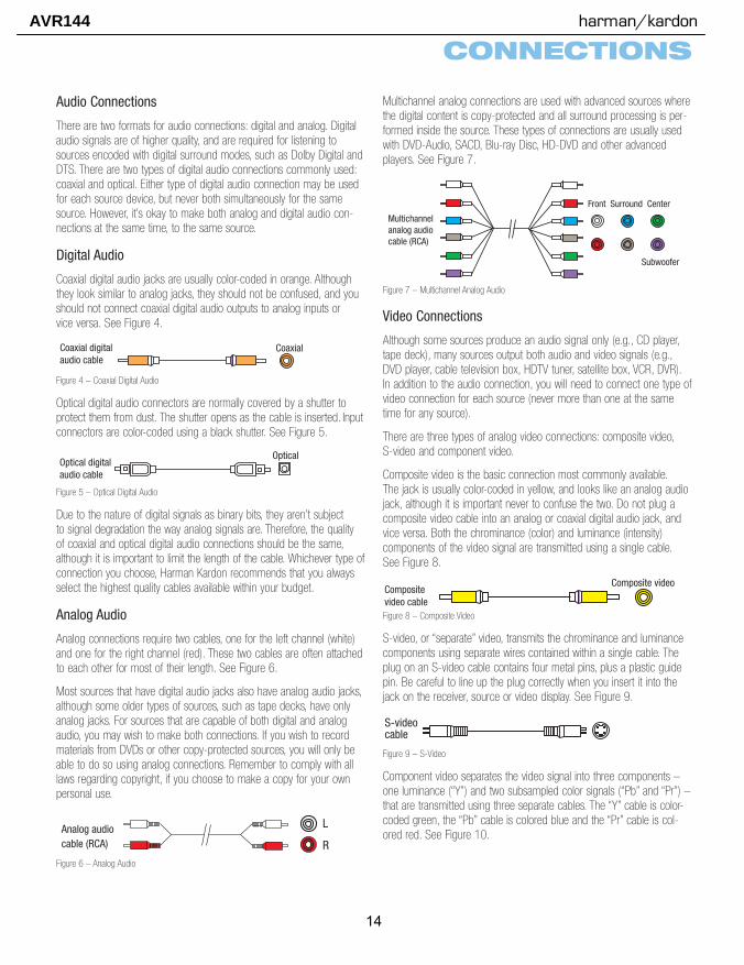
Audio Connections
There are two formats for audio connections: digital and analog. Digitalaudio signals are of higher quality, and are required for listening tosources encoded with digital surround modes, such as Dolby Digital andDTS. There are two types of digital audio connections commonly used:coaxial and optical. Either type of digital audio connection may be usedfor each source device, but never both simultaneously for the samesource. However, it’s okay to make both analog and digital audio con-nections at the same time, to the same source.
Digital Audio
Coaxial digital audio jacks are usually color-coded in orange. Althoughthey look similar to analog jacks, they should not be confused, and youshould not connect coaxial digital audio outputs to analog inputs or vice versa. See Figure 4.
Figure 4 – Coaxial Digital Audio
Optical digital audio connectors are normally covered by a shutter toprotect them from dust. The shutter opens as the cable is inserted. Inputconnectors are color-coded using a black shutter. See Figure 5.
Figure 5 – Optical Digital Audio
Due to the nature of digital signals as binary bits, they aren’t subject to signal degradation the way analog signals are. Therefore, the qualityof coaxial and optical digital audio connections should be the same,although it is important to limit the length of the cable. Whichever type ofconnection you choose, Harman Kardon recommends that you alwaysselect the highest quality cables available within your budget.
Analog Audio
Analog connections require two cables, one for the left channel (white)and one for the right channel (red). These two cables are often attachedto each other for most of their length. See Figure 6.
Most sources that have digital audio jacks also have analog audio jacks,although some older types of sources, such as tape decks, have onlyanalog jacks. For sources that are capable of both digital and analogaudio, you may wish to make both connections. If you wish to recordmaterials from DVDs or other copy-protected sources, you will only beable to do so using analog connections. Remember to comply with alllaws regarding copyright, if you choose to make a copy for your ownpersonal use.
Figure 6 – Analog Audio
Multichannel analog connections are used with advanced sources wherethe digital content is copy-protected and all surround processing is per-formed inside the source. These types of connections are usually usedwith DVD-Audio, SACD, Blu-ray Disc, HD-DVD and other advanced players. See Figure 7.
Figure 7 – Multichannel Analog Audio
Video Connections
Although some sources produce an audio signal only (e.g., CD player,tape deck), many sources output both audio and video signals (e.g.,DVD player, cable television box, HDTV tuner, satellite box, VCR, DVR).In addition to the audio connection, you will need to connect one type ofvideo connection for each source (never more than one at the sametime for any source).
There are three types of analog video connections: composite video,S-video and component video.
Composite video is the basic connection most commonly available.The jack is usually color-coded in yellow, and looks like an analog audiojack, although it is important never to confuse the two. Do not plug a composite video cable into an analog or coaxial digital audio jack, andvice versa. Both the chrominance (color) and luminance (intensity) components of the video signal are transmitted using a single cable.See Figure 8.
Figure 8 – Composite Video
S-video, or “separate” video, transmits the chrominance and luminancecomponents using separate wires contained within a single cable. Theplug on an S-video cable contains four metal pins, plus a plastic guidepin. Be careful to line up the plug correctly when you insert it into thejack on the receiver, source or video display. See Figure 9.
Figure 9 – S-Video
Component video separates the video signal into three components –one luminance (“Y”) and two subsampled color signals (“Pb” and “Pr”) –that are transmitted using three separate cables. The “Y” cable is color-coded green, the “Pb” cable is colored blue and the “Pr” cable is col-ored red. See Figure 10.
S-videocable
Compositevideo cable
Composite video
Multichannelanalog audiocable (RCA)
Front Surround Center
Subwoofer
L
RAnalog audiocable (RCA)
OpticalOptical digitalaudio cable
CoaxialCoaxial digitalaudio cable
HKP1482AVR144-om 9/7/06 3:11 PM Page 17
14
AVR144 harman/kardon

18 18
CONNECTIONS
Figure 10 – Component Video
If it’s available on your video display, component video is recom-mended as the best quality connection, followed by S-video and thencomposite video.
AntennasThe AVR 144 uses separate terminals for the included FM and AMantennas that provide proper reception for the tuner.
The FM antenna uses a 75-ohm F-connector. See Figure 11.
Figure 11 – FM Antenna
The AM loop antenna needs to be assembled. Then connect the twoleads to the screw terminals on the receiver. See Figure 12.
Figure 12 – AM Antenna
Componentvideo cable
HKP1482AVR144-om 9/7/06 3:11 PM Page 18
15
AVR144 harman/kardon

20 20
INSTALLATION
You are now ready to connect your various components to your receiver.Before beginning, make sure that all components, including the AVR 144,are turned completely off and their power cords are unplugged. Don’tplug any of the power cords back in until you have finishedmaking all of your connections.
Remember that your receiver generates heat while it is playing. Select alocation that leaves several inches of space on all sides of the receiver. Itis preferable to avoid completely enclosing the receiver inside a cabinet.It is also preferable to stack components on separate shelves ratherthan directly on top of the receiver. Some surface finishes are delicate.Try to select a location with a sturdy surface finish.
Step One – Connect the SpeakersIf you have not yet done so, place your speakers in the listening roomas described in the Speaker Placement section above.
Connect the center, front left, front right, surround left and surround rightloudspeakers to the corresponding speaker terminals on the AVR 144.Remember to maintain the proper polarity by always connecting thepositive and negative terminals on each speaker to the positive andnegative terminals on the receiver. Use the Connection Color Guide on page 16 as a reference. See Figure 14.
Figure 14 – Speaker Connections
Step Two – Connect the SubwooferConnect the Subwoofer Output on the AVR 144 to the line-level input onyour subwoofer. See Figure 15. Consult the manufacturer’s guide for thesubwoofer for additional information.
Figure 15 – Subwoofer Connection
Step Three – Connect the AntennasConnect the FM and AM antennas to their terminals. See Figure 16.
Figure 16 – Antenna Connections
Step Four – Connect the Source ComponentsUse the worksheets in the Appendix to note which connections you willuse for each of your source devices.
For each source, select a source input (Video 1, Video 2, Video 3, etc.).In Table 2 we recommend connecting certain types of sources to certainsource inputs to make it easier to program and use the remote control.
Decide which audio connections you will use. If your source device hasthem, use either the coaxial digital or the optical digital audio connec-tion. Referring to Table 2, we recommend you connect the DVD sourceto the Coaxial 1 input jack, and the source designated Video 2 to theOptical 1 input jack. However, you may make whatever connections arebest for your system.
In addition to the digital audio connections, we recommend that youconnect the analog audio connections for each source, as a backup tothe digital connections. For sources that don’t have digital audio outputs,you must use the analog audio connections.
For each video source, select one type of video connection. Componentvideo is preferred, but both your source device and your video displaymust have this type of video capability. If either device does not, thenuse S-video. Again, if either your source device or your video displaydoesn’t have S-video connections, then use composite video.
Referring to Table 2, we recommend that you connect the DVD sourceto the Component Video 1 inputs, and any one source designated asVideo 1, Video 2 or Video 3 to the Component Video 2 inputs. However,you may make whatever video connections are best for your system.
FM
AM
AVR 144
AVR 144
SUB
FR FL SR SL
C
AVR 144
HKP1482AVR144-om 9/7/06 3:11 PM Page 20
16
AVR144 harman/kardon

Video 1 Source
Since this source includes audio and video recording output jacks, it isbest suited to a video recorder, such as your VCR or DVR.
Referring to Table 2, connect your recorder to the Video 1 Analog Audioinputs and outputs and to any available Coax or Optical digital audioinput. See Figure 17. Use either the Video 1 S-video or compositevideo input and output if you wish to make recordings. If you don’t planon recording, you may use the Component Video 2 inputs.
Figure 17 – Video 1 A/V Inputs and Outputs, and Digital Audio Inputs
Remember to connect the audio and video output jacks on yourrecorder to the Video 1 or digital audio input jacks on the AVR, and theaudio and video input jacks on your recorder to the Video 1 outputjacks on the AVR.
Device Type AVR 144 Source Input Audio Connections Video Connections
VCR, DVR, PVR, Video 1 • Video 1 Analog (inputs and outputs) • One of component Video 2, Video 1 S-videoTiVo or other and or Video 1 composite video audio/video recorder • Any one available coaxial or optical • For recording, use Video 1 S-video or
digital audio input composite video output, and do not use component video connections at all
Cable TV, satellite, Video 2 • Video 2 Analog and • One of component Video 2, Video 2 HDTV or other • Optical 1 S-video, Video 2 composite videodevice that delivers television programs
TV, game console, Video 3 (front-panel jacks) • Video 3 Analog and • One of component Video 2, Video 3 S-video camera or other • Either Coax 3 or Optical 3 or Video 3 composite videoaudio/video device
DVD Audio/Video, DVD • DVD Analog • Component Video 1SACD, HD-DVD, • 6-Channel inputs (optional) andBlu-ray Disc • Coax 1
CD player CD • CD Analog and • Not required• Any one available coaxial or optical
digital audio input
CDR, MiniDisc, Tape • Tape Analog (inputs and outputs) and • Not requiredcassette • Any one available coaxial or optical
digital audio input
INSTALLATION
NOTE: It’s possible for a source to use none of the connectionsnamed for that source. For example, you might connect yourDVD player to the Component Video 1 inputs and the Coax 1digital audio input. However, we will refer to this source as“DVD”, and in Step Five of the Initial Setup section you will pro-gram the receiver so that these connections are assigned to theDVD source. When you select “DVD” as your source using thefront panel or the remote, the correct connections for your DVDplayer will be used.
We recommend connecting your various sources using the connectionsshown in Table 2 below in order to simplify programming your receiverand remote control. However, you may connect any device to anysource input.
Table 2 – Recommended Source Component Connections
HKP1482AVR144-om 9/7/06 3:11 PM Page 21
17
AVR144 harman/kardon
22
INSTALLATION
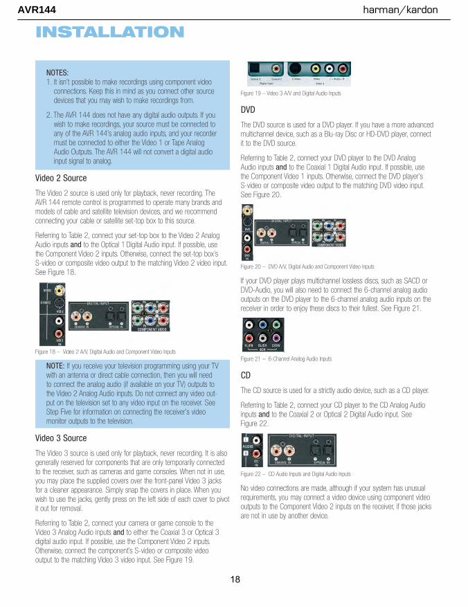
NOTES:1. It isn’t possible to make recordings using component video
connections. Keep this in mind as you connect other sourcedevices that you may wish to make recordings from.
2. The AVR 144 does not have any digital audio outputs. If youwish to make recordings, your source must be connected toany of the AVR 144’s analog audio inputs, and your recordermust be connected to either the Video 1 or Tape AnalogAudio Outputs. The AVR 144 will not convert a digital audioinput signal to analog.
Video 2 Source
The Video 2 source is used only for playback, never recording. TheAVR 144 remote control is programmed to operate many brands andmodels of cable and satellite television devices, and we recommendconnecting your cable or satellite set-top box to this source.
Referring to Table 2, connect your set-top box to the Video 2 AnalogAudio inputs and to the Optical 1 Digital Audio input. If possible, use the Component Video 2 inputs. Otherwise, connect the set-top box’s S-video or composite video output to the matching Video 2 video input.See Figure 18.
Figure 18 – Video 2 A/V, Digital Audio and Component Video Inputs
NOTE: If you receive your television programming using your TVwith an antenna or direct cable connection, then you will needto connect the analog audio (if available on your TV) outputs tothe Video 2 Analog Audio inputs. Do not connect any video out-put on the television set to any video input on the receiver. SeeStep Five for information on connecting the receiver’s videomonitor outputs to the television.
Video 3 Source
The Video 3 source is used only for playback, never recording. It is alsogenerally reserved for components that are only temporarily connectedto the receiver, such as cameras and game consoles. When not in use,you may place the supplied covers over the front-panel Video 3 jacksfor a cleaner appearance. Simply snap the covers in place. When youwish to use the jacks, gently press on the left side of each cover to pivotit out for removal.
Referring to Table 2, connect your camera or game console to theVideo 3 Analog Audio inputs and to either the Coaxial 3 or Optical 3digital audio input. If possible, use the Component Video 2 inputs.Otherwise, connect the component’s S-video or composite video output to the matching Video 3 video input. See Figure 19.
Figure 19 – Video 3 A/V and Digital Audio Inputs
DVD
The DVD source is used for a DVD player. If you have a more advancedmultichannel device, such as a Blu-ray Disc or HD-DVD player, connectit to the DVD source.
Referring to Table 2, connect your DVD player to the DVD Analog Audio inputs and to the Coaxial 1 Digital Audio input. If possible, use the Component Video 1 inputs. Otherwise, connect the DVD player’s S-video or composite video output to the matching DVD video input.See Figure 20.
Figure 20 – DVD A/V, Digital Audio and Component Video Inputs
If your DVD player plays multichannel lossless discs, such as SACD orDVD-Audio, you will also need to connect the 6-channel analog audiooutputs on the DVD player to the 6-channel analog audio inputs on thereceiver in order to enjoy these discs to their fullest. See Figure 21.
Figure 21 – 6-Channel Analog Audio Inputs
CD
The CD source is used for a strictly audio device, such as a CD player.
Referring to Table 2, connect your CD player to the CD Analog Audioinputs and to the Coaxial 2 or Optical 2 Digital Audio input. See Figure 22.
Figure 22 – CD Audio Inputs and Digital Audio Inputs
No video connections are made, although if your system has unusualrequirements, you may connect a video device using component videooutputs to the Component Video 2 inputs on the receiver, if those jacksare not in use by another device.
HKP1482AVR144-om 9/7/06 3:11 PM Page 22
18
AVR144 harman/kardon

23
Tape
The Tape source is used for audio-only recorders, such as a CDR,MiniDisc or cassette deck.
Referring to Table 2, connect your recorder to the Tape AnalogAudio inputs and outputs, and to any available digital audio input.See Figure 23.
Figure 23 – Tape Audio Inputs and Outputs, and Digital Audio Inputs
NOTE: You will not be able to make digital audio recordings usingthe AVR 144. Make sure your source is connected to any ofthe AVR 144’s analog audio inputs, and connect your recorderto either the Video 1 or Tape Analog Audio Outputs. The AVR 144will not convert a digital audio input signal to analog.
Remember to connect the output jacks on your recorder to the Tape or digital audio input jacks on the AVR, and the input jacks on yourrecorder to the Tape output jacks on the AVR.
No video connections are made.
Step Five – Connect Video DisplayOnly video connections should be made between the receiver and yourvideo display (TV), unless your TV is the source for your television pro-gramming (see note above).
You will need to make a video connection for each type of video usedfor your sources. In addition, even if you didn’t use S-video or compos-ite video for any of your sources, you will still need to use one of thesetwo video monitor connections in order to view the AVR 144’s on-screen menus and displays.
First, determine what types of video your display is capable of handling.Remember that component video is preferred, followed by S-video andthen composite video. Ideally, this guided you in selecting the video con-nections for your sources.
Next, note which types of video connections you used for your sourcedevices. Make sure you didn’t use a better type of video connection fora source than your video display can handle. If so, you will need to dis-connect the source and use a video connection that’s compatible withyour display.
If you used component video for any sources, connect the ComponentVideo Monitor outputs on the receiver to one set of component videoinputs on your display. Make a note of how these inputs are labeled onthe display. See Figure 24.
Figure 24 – Component Video Monitor Outputs
If you used S-video for any sources, or if all of your sources used com-ponent video, connect the S-video Monitor output on the receiver to anS-video input on your display. Make a note of how the input is labeled.See Figure 25.
If you used composite video for any sources, connect the compositevideo Monitor output on the receiver to a composite video input on thedisplay. Again, make a note of how this input is labeled on the display.See Figure 25.
Figure 25 – S-Video and Composite Video Monitor Outputs
Consult the manual for your TV to make sure you understand how toselect each video input. As you play different source devices that usedifferent types of video connections, you will need to remember toselect the correct video input on your video display.
Step Six – Plug in AC PowerHaving made all of your wiring connections, it is now time to plug eachcomponent’s AC power cord into a working outlet.
Before plugging the AVR 144’s AC Power Cord into an electrical outlet,make sure that the Master Power Switch on the front panel is poppedout so that the word OFF appears on its top. Gently press the button toturn the switch off. This will prevent the possibility of damaging the AVRin case of a transient power surge.
Step Seven – Insert Batteries in RemoteThe AVR 144 remote control uses three AAA batteries, which areincluded.
To remove the battery cover located on the back of the remote, firmlypress the ridged depression and slide the cover towards the top of the remote.
Insert the batteries as shown in the diagram, making sure to observe the correct polarity. See Figure 26.
Figure 26 – Remote Battery Compartment
When using the remote, remember to point the lens toward the frontpanel of the AVR 144. Make sure no objects, such as furniture, areblocking the remote’s path to the receiver. Bright lights, fluorescent lightsand plasma video displays may interfere with the remote’s functioning.The remote has a range of about 20 feet, depending on the lightingconditions. It may be used at an angle of up to 30 degrees to eitherside of the AVR.
INSTALLATION
HKP1482AVR144-om 9/7/06 3:11 PM Page 23
19
AVR144 harman/kardon

24
INSTALLATION
If the remote seems to operate intermittently, or if pressing a button on the remote does not cause the AVR Selector or one of the InputSelectors to light up, then make sure the batteries have been insertedcorrectly, or replace all three batteries with fresh ones.
Step Eight – Program Sources Into the RemoteThe AVR 144 remote is capable of controlling not only the receiver,but it may also be programmed to control many brands and models ofVCRs, DVD players, CD players, cable boxes, satellite receivers, cassettedecks and TVs.
It may help to think of the remote as a book with pages. Each page rep-resents the button functions for a different device. In order to access thefunctions for a particular device, you first need to turn to that page. Thisis done by pressing the AVR Button to access the codes that control thereceiver, or the Input Selector buttons to access the codes for thedevices programmed into the remote.
At the factory, the AVR 144’s codes and the codes to control manyHarman Kardon DVD and CD players are preprogrammed. If you haveother source devices in your system, follow these steps to program thecorrect codes into the remote.
1. Using the codes in Tables A9–A15 of the Appendix, look up theproduct type (e.g., DVD, cable TV box) and the brand name of yoursource. The number(s) listed are potential candidates for the correctcode set for your particular device.
2. Turn on your source device.
3. Put the remote into Program mode by pressing and holding the InputSelector and the Mute button simultaneously until the LED on theremote starts to flash, and then releasing the buttons. See Figure 27.
Figure 27 – Input Selectors
4. Enter a code from Step 1 above.
a) If the device turns off, then press the Input Selector again to acceptthe code, which will flash. The remote will exit the Program mode.
b) If the device does not turn off, try entering another code. If you run out of codes, you may search through all of the codes in theremote’s library for that product type by pressing the ⁄ or ¤
button repeatedly until the device turns off. When the device turnsoff, enter the code by pressing the Input Selector, which will flash.The remote then exits Program mode.
5. Once you have accepted a code, it’s a good idea to try using someother functions to control the device. Sometimes manufacturers
use the same Power code for several different models, while othercodes will vary. You may wish to repeat this process until you’ve pro-grammed a satisfactory code set that operates most of the functionsyou frequently use.
6. You may find out which code number you have programmed bypressing and holding the Input Selector and Mute Button simultane-ously to enter the Program mode. Then press the Set Button, and theLED will blink in the code sequence. One blink represents “1”, twoblinks for “2”, and so forth. A series of many fast blinks represents “0”. Record the codes programmed for each device here.
Table 3 – Remote Control Codes
If you are unable to locate a code set that correctly operates yoursource device, it will not be possible to use the AVR remote to controlthat device. However, you may still connect the source to the AVR 144and operate it using the device’s original remote control. Alternatively,you may wish to consider purchasing Harman Kardon’s optional TC 30activity-based remote, which is programmed by accessing a large data-base of product codes on the Internet. The TC 30 is also capable of“learning” codes from your device’s original remote.
Most of the button labels on the remote describe the button’s functionwhen used to control the AVR 144. However, the button may perform avery different function when used to control another device. Refer to theRemote Control Function List, Table A8 in the Appendix, for a list ofeach button’s functions with the various product types.
If you wish, you may program Macros, which are preprogrammed codesequences that execute many code commands with a single buttonpress. You may also program “punch-through” codes, which allow theremote to operate the volume, channel or transport controls of anotherdevice without having to switch the remote to the mode for that device.See pages 42 – 43 for instructions on these advanced programmingfunctions.
NOTE: The AVR 144 remote is preprogrammed to operate thetransport controls of Harman Kardon DVD players when the AVRor the Video 2 (cable/satellite) or Video 3 (TV) source is selected.The volume and mute controls operate the AVR when anydevice except Tape has been selected. You may change thispunch-through programming at any time.
Source Input Product Type Remote Control Code(circle one)
Video 1 VCR, PVRVideo 2 Cable, SatelliteVideo 3 TVDVD DVDCD CD, CDRTape Cassette
HKP1482AVR144-om 9/7/06 3:11 PM Page 24
20
AVR144 harman/kardon
25
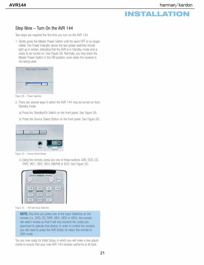
Step Nine – Turn On the AVR 144Two steps are required the first time you turn on the AVR 144.
1. Gently press the Master Power Switch until the word OFF is no longervisible. The Power Indicator above the two power switches shouldlight up in amber, indicating that the AVR is in Standby mode and isready to be turned on. See Figure 28. Normally, you may leave theMaster Power Switch in the ON position, even when the receiver isnot being used.
Figure 28 – Power Switches
2. There are several ways in which the AVR 144 may be turned on fromStandby mode.
a) Press the Standby/On Switch on the front panel. See Figure 28.
b) Press the Source Select Button on the front panel. See Figure 29.
Figure 29 – Source Select Button
c) Using the remote, press any one of these buttons: AVR, DVD, CD,TAPE, VID1, VID2, VID3, AM/FM or 6CH. See Figure 30.
Figure 30 – AVR and Input Selectors
NOTE: Any time you press one of the Input Selectors on theremote (i.e., DVD, CD, TAPE, VID1, VID2 or VID3), the remotewill switch modes so that it will only transmit the codes pro-grammed to operate that device. In order to control the receiver,you will need to press the AVR Button to return the remote toAVR mode.
You are now ready for Initial Setup, in which you will make a few adjust-ments to ensure that your new AVR 144 receiver performs at its best.
INSTALLATION
HKP1482AVR144-om 9/7/06 3:11 PM Page 25
21
AVR144 harman/kardon

OPERATION
Now that you have installed your system components and completed atleast a basic configuration of your receiver, you are ready to beginenjoying your home theater system.
Turning On the AVR 144Gently press the Master Power Switch until the word OFF is no longer visi-ble. The Power Indicator above the two power switches should light up inamber. This indicates that the AVR is in Standby mode and is ready to beturned on. Normally, you may leave the Master Power Switch in the ONposition, even when the receiver is not being used. See Figure 41.
Figure 41 – Power Switches
There are several ways in which the AVR 144 may be turned on:
a) Press the Standby/On Switch on the front panel. See Figure 41.
b) Press the Source Select Button on the front panel. See Figure 42.
Figure 42 – Source Select Button
c) Using the remote, press any one of these buttons: AVR, DVD, CD,TAPE, VID1, VID2, VID3, AM/FM or 6CH. See Figure 43.
Figure 43 – AVR and Input Selectors
NOTE: Any time you press one of the remote’s Input Selectors(i.e., DVD, CD, TAPE, VID1, VID2 or VID3), the remote will switchmodes so that it will only transmit the codes programmed tooperate that device. In order to control the receiver, you will needto press the AVR Button to return the remote to AVR mode.
To turn the receiver off, press either the Standby/On Switch on the frontpanel, or press the AVR Button and the OFF Button on the remote.Unless the receiver will not be used for an extended period of time (for example, if you will be on vacation), it is not necessary to turn offthe Master Power Switch. When the Master Power Switch is turned off,any settings you have programmed, including system configuration andpreset radio stations, will be preserved for up to four weeks.
Sleep TimerYou may program the AVR to play for up to 90 minutes and then turnoff automatically using the sleep timer.
Press the Sleep Button on the remote, and the time until turn-off will bedisplayed. Each additional press of the Sleep Button will reduce the timeuntil turn-off by 10 minutes, until the OFF setting is reached, which dis-ables the sleep timer. See Figure 44.
Figure 44 – Sleep Button
When the sleep timer has been set, the front-panel display will automati-cally dim to half-brightness. If you press any button on the remote orfront panel, the display will return to full-brightness. The display will dimagain several seconds after your last command.
If you press the Sleep Button after the timer has been set, the remainingtime until turn-off will be displayed. You may press the Sleep Button tochange the time until turn-off. Pressing and holding the Sleep Button willdisable the sleep timer, and the SLEEP OFF message will appear.
Volume ControlThe volume may be adjusted either by turning the knob on the frontpanel (clockwise to increase volume or counterclockwise to decreasevolume), or by pressing the Volume Control Buttons on the remote. SeeFigure 45. The volume is displayed as a negative number of decibels(dB) below the 0dB reference point, and may be changed in 0.5dBincrements. Unlike some volume controls on other products, 0dB is themaximum volume for the AVR 144. Although it’s physically possible toturn the volume to a higher level, doing so may damage your hearingand your speakers. For certain more dynamic audio materials, even 0dBmay be too high, allowing for damage to equipment.
Figure 45 – Volume Controls
HKP1482AVR144-om 9/7/06 3:12 PM Page 32
22
AVR144 harman/kardon

33
OPERATION
Remember that the AVR 144 is designed to reproduce audio with aminimum amount of distortion. This clarity may lead you to believe thatyour hearing and the equipment can handle higher volumes. We urgecaution with regard to volume levels.
Mute FunctionTo temporarily mute all speakers and the headphones, press the MuteButton on the remote. See Figure 46. Any recording in progress will notbe affected. The MUTE message will flash in the display as a reminder.To restore normal audio, either press the Mute Button again, or adjustthe volume. Turning off the AVR will also end muting.
Figure 46 – Mute Button
Tone ControlsYou may boost or cut either the treble or the bass frequencies by up to 10dB in 2dB increments.
Using the remote, press the Tone Mode Button once. See Figure 47.This will indicate whether the tone controls are in or out of the circuitry.If you wish to return the tone controls to 0, or “flat” response, press the⁄/¤ Buttons until the TONE OUT message appears, which preservesany changes you have made to the bass or treble settings for later use.To reactivate your changes, the tone control must again be set to TONE IN.
With the TONE IN message displayed, press the Tone Mode Buttonrepeatedly to access TREBLE MODE and BASS MODE. Use the⁄/¤ Buttons to change the treble or bass settings, as desired. Thedisplay will return to normal a few seconds after your last command.
Figure 47 – Tone Button
You may alternatively adjust the tone controls using the full-OSD menusystem. Press the OSD Button on the remote to view the Master Menu.The cursor will be pointing to the INPUT SETUP line; press the SetButton to display that menu. You will be able to view the tone settings. Ifyou wish to make any changes to the TONE, BASS or TREBLE settings,use the arrow keys on the remote to move the cursor to the line youwish to change. Once you have changed the setting using the ‹/›Buttons, simply move the cursor up or down to a different line; it isn’tnecessary to press the Set Button to enter the new setting. When youhave finished, either wait until the display times out and disappears,
press the OSD Button to clear the display, or move the cursor to theBACK TO MASTER MENU line if you wish to make other changes usingthe menu system.
NOTE: The AVR 144 does not have any conventional balancecontrol. The output level calibration process compensates for anycharacteristics of your room or speakers, and we recommendthat you leave the settings as they are after the speakers havebeen calibrated. However, you may manually adjust the levels ofthe left and right channels – decreasing one and increasing theother by the same amount – using the Channel Adjust submenu.This achieves the same effect as a balance control.
HeadphonesPlug the 1/4" plug on a pair of headphones into the headphone jack on the front of the receiver for private listening. See Figure 48. The first time you use the headphones, the DOLBY H:BP message will bedisplayed, indicating that Dolby Headphone surround processing is inthe bypass mode, which delivers a conventional 2-channel signal to the headphones.
Figure 48 – Headphone Jack
Press the Surround Select Button on the front panel, or the DolbyButton on the remote, to switch to Dolby Headphone virtual surroundprocessing, indicated by the DOLBY H:DH message. Dolby Headphonedelivers an enhanced sound field that emulates a 5.1-channel speakersystem. No other surround modes are available for the headphones.
Source SelectionPress the front-panel Source Select Button to scroll through thesources. The left side of the button scrolls down the list that appears inthe display; the right side scrolls upward. For direct access to the tuner,press the Tuner Band Button, which switches to the last-used band andfrequency. See Figure 49. For direct access to any source, press itsInput Selector on the remote (see Figure 43).
Figure 49 – Source Select and Tuner Band Buttons
The AVR 144 will switch to the audio and video inputs assigned to thatsource. If you set the BASS MGR setting in the Speaker X-Over menuto INDEPENDENT, the AVR 144 will change the speaker size configura-tion to the one you programmed for the source. If you selected a sur-round mode for the source, the AVR 144 will switch to that mode.
HKP1482AVR144-om 9/7/06 3:12 PM Page 33
23
AVR144 harman/kardon
34
OPERATION
The source name will appear in the upper line of the front-panel display.If you retitled the source, only the new title will appear. Otherwise, theaudio input assigned to the source (analog or one of the digital audioinputs) will also appear. The surround mode will be displayed on thelower line. The same information will also appear on screen in the semi-OSD, unless you have set the semi-OSD to OFF in the SystemSetup menu (see Advanced Functions section).
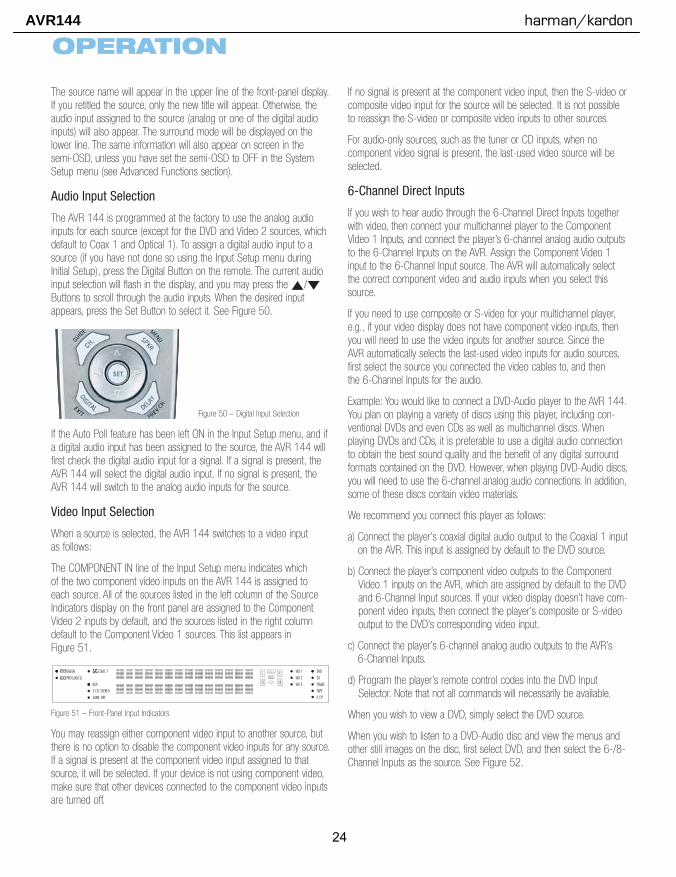
Audio Input Selection
The AVR 144 is programmed at the factory to use the analog audioinputs for each source (except for the DVD and Video 2 sources, whichdefault to Coax 1 and Optical 1). To assign a digital audio input to asource (if you have not done so using the Input Setup menu duringInitial Setup), press the Digital Button on the remote. The current audioinput selection will flash in the display, and you may press the ⁄/¤Buttons to scroll through the audio inputs. When the desired inputappears, press the Set Button to select it. See Figure 50.
Figure 50 – Digital Input Selection
If the Auto Poll feature has been left ON in the Input Setup menu, and ifa digital audio input has been assigned to the source, the AVR 144 willfirst check the digital audio input for a signal. If a signal is present, theAVR 144 will select the digital audio input. If no signal is present, theAVR 144 will switch to the analog audio inputs for the source.
Video Input Selection
When a source is selected, the AVR 144 switches to a video input as follows:
The COMPONENT IN line of the Input Setup menu indicates which of the two component video inputs on the AVR 144 is assigned to each source. All of the sources listed in the left column of the SourceIndicators display on the front panel are assigned to the ComponentVideo 2 inputs by default, and the sources listed in the right columndefault to the Component Video 1 sources. This list appears in Figure 51.
Figure 51 – Front-Panel Input Indicators
You may reassign either component video input to another source, butthere is no option to disable the component video inputs for any source.If a signal is present at the component video input assigned to thatsource, it will be selected. If your device is not using component video,make sure that other devices connected to the component video inputsare turned off.
If no signal is present at the component video input, then the S-video orcomposite video input for the source will be selected. It is not possibleto reassign the S-video or composite video inputs to other sources.
For audio-only sources, such as the tuner or CD inputs, when no component video signal is present, the last-used video source will beselected.
6-Channel Direct Inputs
If you wish to hear audio through the 6-Channel Direct Inputs togetherwith video, then connect your multichannel player to the ComponentVideo 1 Inputs, and connect the player’s 6-channel analog audio outputsto the 6-Channel Inputs on the AVR. Assign the Component Video 1input to the 6-Channel Input source. The AVR will automatically selectthe correct component video and audio inputs when you select thissource.
If you need to use composite or S-video for your multichannel player,e.g., if your video display does not have component video inputs, thenyou will need to use the video inputs for another source. Since the AVR automatically selects the last-used video inputs for audio sources,first select the source you connected the video cables to, and then the 6-Channel Inputs for the audio.
Example: You would like to connect a DVD-Audio player to the AVR 144.You plan on playing a variety of discs using this player, including con-ventional DVDs and even CDs as well as multichannel discs. When playing DVDs and CDs, it is preferable to use a digital audio connectionto obtain the best sound quality and the benefit of any digital surroundformats contained on the DVD. However, when playing DVD-Audio discs,you will need to use the 6-channel analog audio connections. In addition,some of these discs contain video materials.
We recommend you connect this player as follows:
a) Connect the player’s coaxial digital audio output to the Coaxial 1 inputon the AVR. This input is assigned by default to the DVD source.
b) Connect the player’s component video outputs to the ComponentVideo 1 inputs on the AVR, which are assigned by default to the DVDand 6-Channel Input sources. If your video display doesn’t have com-ponent video inputs, then connect the player’s composite or S-videooutput to the DVD’s corresponding video input.
c) Connect the player’s 6-channel analog audio outputs to the AVR’s 6-Channel Inputs.
d) Program the player’s remote control codes into the DVD InputSelector. Note that not all commands will necessarily be available.
When you wish to view a DVD, simply select the DVD source.
When you wish to listen to a DVD-Audio disc and view the menus andother still images on the disc, first select DVD, and then select the 6-/8-Channel Inputs as the source. See Figure 52.
DIGITAL LOGIC 7 VID 1 DVD
CD
FMAM
TAPE
6 CH
VID 2
VID 3
PRO LOGIC
DSP
5 CH. STEREO
SURR. OFF
HKP1482AVR144-om 9/7/06 3:12 PM Page 34
24
AVR144 harman/kardon

35
OPERATION
Figure 52 – 6-Channel Input Selector
NOTE: The 6-Channel Inputs pass the incoming signals directlyto the volume control, without digitizing or processing them.Therefore, you will need to configure bass management settings(i.e., speaker size, delay and output level) on your source deviceso that they match the settings you programmed using theManual Setup menu. Consult the owner’s guide for your multi-channel player for more information.
Using the TunerThe AVR 144’s built-in tuner may be selected in one of three ways (seeFigure 53):
1. Press the Source Selector Button on the front panel repeatedly untilthe tuner is selected. The last-used band (AM or FM) will be active.
2. Press the Tuner Band Button (marked AM/FM). Press this buttonagain to switch bands.
3. Press the Tuner Input Selector (marked AM/FM) on the remote. Pressthis button again to switch bands.
Figure 53 – Tuner Input Selection
Radio stations may be selected in one of four ways (see Figure 54):
1. If you know the frequency number, enter it directly by first pressingthe Direct Button on the remote, and then using the Numeric Keys.
2. After you have programmed Preset stations (see below), either enterthe Preset number (1 through 30) using the remote or use the front-panel Preset Stations Button to scroll through the list of presets.
3. In Auto tuning mode, with each press of the Tuning Buttons (front-panel or remote) the AVR 144 will scan in the chosen direction until astation with acceptable signal strength is detected. Press the TuningButton again to stop scanning.
4. In Manual tuning mode, with each press of the Tuning Buttons theAVR 144 will tune the next frequency increment (0.1MHz for FM, or10kHz for AM) in the selected direction. Press and hold the TuningButton for faster scanning.
Figure 54 – Tuning a Station
Press the Tuning Mode Button (TUN-M on the remote) to switchbetween Auto and Manual tuning modes. When an FM station has beentuned, pressing the Tuning Mode Button will switch between stereo andmono tuning, which may improve reception of weaker stations. SeeFigure 55.
Figure 55 – Tuning Mode
To store a station in one of the 30 presets (see Figure 56):
1. Tune the desired station.
2. Press the Memory Button on the remote.
3. Use the Numeric Keys to enter the desired preset number.
Figure 56 – Storing a Preset Station
RecordingTwo-channel analog audio signals, as well as composite and S-videosignals, are normally available at the appropriate recording outputs. Thus,to make a recording, you need only make sure to connect your audio orvideo recorder to the appropriate output jacks, as described in theInstallation section, insert blank media and make sure the recorder isturned on and recording while the source is playing.
NOTES:1. Analog audio signals are not converted to digital form, and
digital audio signals are not converted to analog audio form.
2. The AVR 144 is not designed to make digital audio record-ings. Make sure your source device is connected to one ofthe AVR 144’s analog audio inputs, and connect yourrecorder to either the Video 1 or Tape analog audio outputs.
3. Component video sources are not available for recording.
4. Please make certain that you are aware of any copyrightrestrictions on any material you record. Unauthorized duplicationof copyrighted materials is prohibited by federal law.
HKP1482AVR144-om 9/7/06 3:12 PM Page 35
25
AVR144 harman/kardon

36
OPERATION
Selecting a Surround ModeSurround mode selection can be as simple or sophisticated as yourindividual system and tastes. Feel free to experiment with the manyavailable surround modes on the AVR 144, and you may find a few thatbecome your favorites for certain sources or program types. Althoughmore detailed information on surround modes may be found in theAdvanced Functions section, it is easy to select any of the modes available at a given time:
To select a surround mode using the front-panel controls, press theSurround Mode Button repeatedly until the desired group of modes isselected: Logic 7, Dolby, DTS, DSP or Stereo. Then press the SurroundSelect Button repeatedly to select the desired mode within the group.See Figure 57.
Figure 57 – Select a Surround Mode (Front Panel)
To select a surround mode using the remote control, locate the buttondedicated to the desired group of modes: Logic 7, Dolby Sur, DTS Sur,DTS Neo:6, Surr (DSP) or Stereo. Press that button repeatedly to selectthe desired mode. See Figure 58.
Figure 58 – Select a Surround Mode (Remote)
To select a surround mode using the full-OSD menu system, press theOSD Button to display the Master Menu. Navigate to the SURROUNDSELECT line and press the Set Button to view the Surround Selectmenu. Each of the major surround mode groups is listed here. Selectthat group to access the MODE setting for selection of an individualmode. As explained in the Advanced Functions section, there are alsosome additional settings that may be made.
You are now ready to enjoy the best in home theater entertainment,using your AVR 144. As you become more familiar with the receiver,you may wish to explore some of its advanced functions, which aredescribed in the following section.
HKP1482AVR144-om 9/7/06 3:12 PM Page 36
26
AVR144 harman/kardon

45
TROUBLESHOOTING GUIDESYMPTOM CAUSE SOLUTION
Unit does not function when Main • No AC Power • Make certain AC power cord is plugged into Power Switch is pushed a live outlet
• Check to see whether outlet is switch-controlled
Display lights, but no sound • Intermittent input connections • Make certain that all input and speaker connections or picture are secure
• Mute is on • Press Mute Button• Volume control is down • Turn up volume control
No sound from any speaker; • Amplifier is in protection mode • Check speaker wire connections for shorts at receiver and light around power switch is red due to possible short speaker ends
• Amplifier is in protection mode • Contact your local Harman Kardon service centerdue to internal problems
No sound from surround or • Incorrect surround mode • Select a mode other than Stereocenter speakers • Input is monaural • There is no surround information from mono sources
• Incorrect configuration • Check speaker mode configuration • Stereo or Mono program material • The surround decoder may not create center- or rear-channel
information from nonencoded programs
Unit does not respond to • Weak batteries in remote • Change remote batteriesremote commands • Wrong device selected • Press the AVR selector
• Remote sensor is obscured • Make certain front panel sensor is visible to remoteor connect an optional remote sensor
Intermittent buzzing in tuner • Local interference • Move unit or antenna away from computers, fluorescent lights, motors or other electrical appliances
Letters flash in the channel indicator • Digital audio feed paused • Resume play for DVDdisplay and digital audio stops • Check that Digital Input is selected
In addition to the items shown above, additional information on troubleshooting possible problems with your AVR 145, or installation-related issues, maybe found in the list of "Frequently Asked Questions" which is located in the Product Support section of our Web site at www.harmankardon.com.
AVR 145 OM (New) 8/4/06 1:19 PM Page 45
Erasing Macros It isn’t possible to “edit” a command within a macro. However, you may erase the macro as follows: 1. Simultaneously press and hold the Mute Button and the Macro Button containing the macro until the LED flashes. 2. Press the Surround Button to erase the macro. Resetting the Remote To reset the remote to its factory defaults, enter Program mode by simultaneously pressing and holding any Input Selector and the Mute Button. When the LED flashes, enter the code “333”. When the LED goes out, the remote will have been fully reset. Processor Reset There may be instances where you wish to fully reset the AVR 145 to its factory defaults, or the unit may behave erratically after a power surge. For erratic behavior, we recommend you try turning the Master Power Switch off and unplugging the AC Power Cord for at least three minutes. Try plugging the cord back in and turning the receiver back on. If this doesn’t work, you may want to try a system reset. NOTE: A system reset erases all user configurations, including speaker and level settings and tuner presets. After a reset, you will need to re-enter all of these settings. To reset the AVR 145, place the receiver in Standby mode (press the front-panel Standby/On Switch so that the Power Indicator turns amber). Then press and hold the front-panel Tone Mode Button for at least five seconds until the RESET message appears in the display. If the receiver still does not function correctly after a processor reset, contact an authorized Harman Kardon service center for assistance. Service centers may be located by visiting our Web site at www.harmankardon.com. Memory If the AVR 145 is unplugged or experiences a power outage, it will retain user settings for up to four weeks.
27
AVR144 harman/kardon
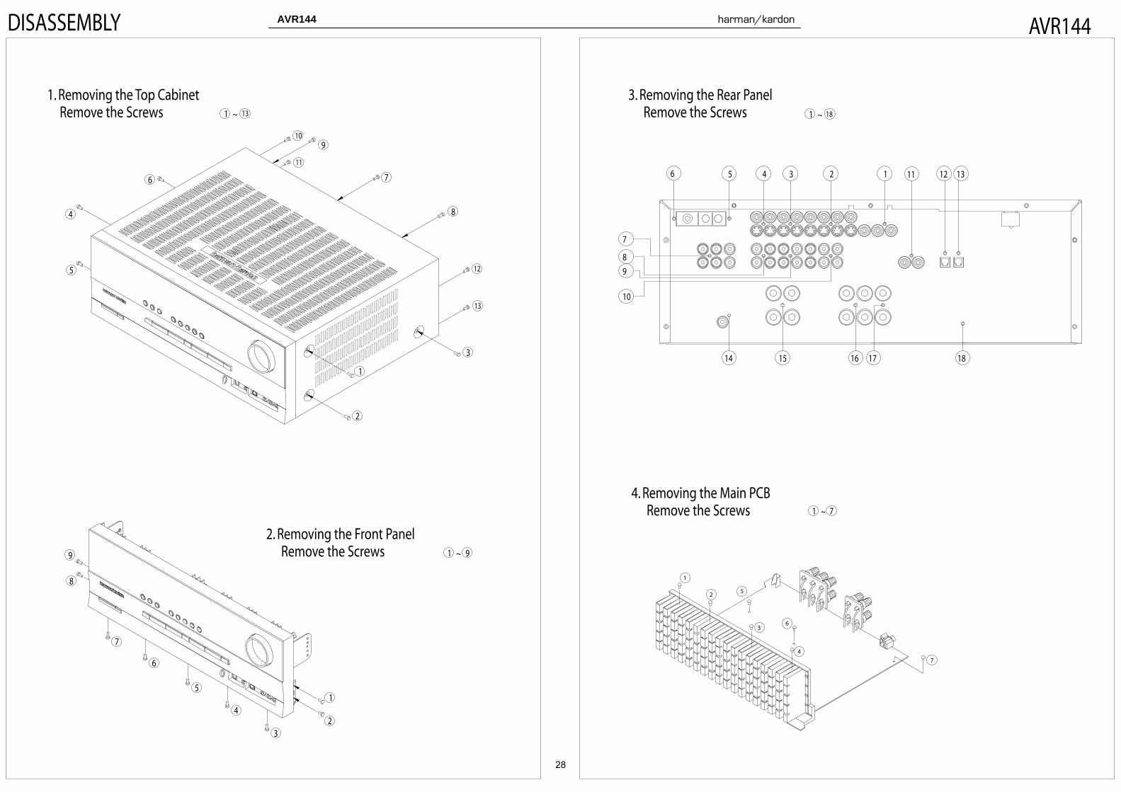
1
2
1
1. Removing the Top Cabinet Remove the Screws
5
4
6
DISASSEMBLY
~ 13
11
10
7
9
13
3
12
8
7
5
6
8
9
4
32
1
Remove the Screws2. Removing the Front Panel
1 9~
63
4
7
Remove the Screws4. Removing the Main PCB
1
25
~1 7
13
18
~1 18 Remove the Screws
10
9
8
14
7
6 5
15 16 17
3. Removing the Rear Panel
AVR144
114 3 2 1 12
28
AVR144 harman/kardon
AVR144 DISASSEMBLY PROCEDURES
1 TOP-CABINET (21) REMOVAL
1. Remove 13 screws (S1,S7) and then remove the Top-cabinet. 2 FRONT PANEL ASS’Y REMOVAL
1. Remove the Top-cabinet, referring to the previous step1. 2. Disconnect the card cable between connector (CN72-17p) on the Fip PCB (37-1) and connector (CN72) on the Input PCB (39-1). 3. Disconnect the lead wire (BN81-8P) on the Fip PCB (37-1) from connector (CN81) on the Trans PCB (40-4). 4. Disconnect the lead wire (BN22-6P) on the Phone PCB (37-5) from connector (CN22) on the Input PCB (39-1). 5. Disconnect the lead wire (BN18-5P) on the Phone PCB (37-5) from connector (CN18) on the Input PCB (39-1) 6. Disconnect the lead wire (BN10-4P) on the Volume PCB (37-6) from connector (CN10) on the Input PCB (39-1) 7. Disconnect the lead wire (BN41-6P) on the Volume PCB (37-6) from connector (CN41) on the Video PCB (41) 8. Remove 1 screw (S10) and then lead wire (JW82-1P,JW83-1P) on the Phone PCB (37-5). 9 .Remove 1screw (S10) and then lead wire (JW84-1P) on the Volume PCB (37-3). 10. Remove 10 screws (S1) and then remove the Front Panel ASS’Y.
3 VOLUME PCB (37-6) REMOVAL 1. Remove the Top-cabinet, referring to the previous step1.
2. Remove the Front Panel ASS’Y, referring to the previous step 2. 3. Pull out the Volume Knob ASS’Y. 4. Disconnect connector (CN84) on the Volume PCB (37-6) from the lead wire (BN84-5P) on the Fip PCB (37-1). 5. Remove 8 screws (S2,S14), and then remove the Volume PCB (37-6).
4 PHONE PCB (37-5) REMOVAL 1. Remove the Top-cabinet, referring to the previous step 1.
2. Remove the Front Panel ASS’Y, referring to the previous step 2. 3.. Disconnect connector (CN85)on the Phone PCB (37-5) from the lead wire (BN85-2P) on the Fip PCB (37-1). 4. Remove 2 screws (S2) and then remove the Phone PCB (37-5). .
5 POWER LED PCB (37-3) REMOVAL 1. Remove the Top-cabinet, referring to the previous step1.
2. Remove the Front Panel ASS’Y, referring to the previous step 2. 3. Disconnect connector (CN88) on the Power Led PCB (37-3) from the lead wire (BN88-4P) on the Fip PCB (37-1) . 4. Remove 2 screws (S2) and then remove the Power led PCB (37-3).
6 FIP PCB (37-1) REMOVAL 1. Remove the Top-cabinet, referring to the previous step 1.
2. Remove the Front Panel ASS’Y, referring to the previous step 2. 3. Disconnect the lead wire (BN84-5P) on the Fip PCB (37-1) from connector (CN84) on the Volume PCB (37-6). 4. Disconnect the lead wire (BN85-2P) on the Fip PCB (37-1) from connector (CN85) on the Phone PCB (37-5). 5. Disconnect the lead wire (BN88-4P) on the Fip PCB (37-1) from connector (CN88) on the Power Led PCB (37-3). 6. Remove 3 screws (S2) and then remove the Guide PCB (37-8) & the Fip PCB (37-1).
29
AVR144 harman/kardon
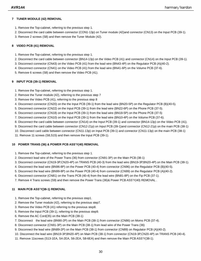
7 TUNER MODULE (42) REMOVAL
1. Remove the Top-cabinet, referring to the previous step 1. 2. Disconnect the card cable between connector (CON1-13p) on Tuner module (42)and connector (CN13) on the Input PCB (39-1). 3. Remove 2 screws (S8) and then remove the Tuner Module (42).
8 VIDEO PCB (41) REMOVAL
1. Remove the Top-cabinet, referring to the previous step 1. 2. Disconnect the card cable between connector (BN14-13p) on the Video PCB (41) and connector (CN14) on the Input PCB (39-1). 3. Disconnect connector (CN43) on the Video PCB (41) from the lead wire (BN43-4P) on the Regulator PCB (A)(40-2). 4. Disconnect connector (CN41) on the Video PCB (41) from the lead wire (BN41-6P) on the Volume PCB (37-6). 5. Remove 6 screws (S8) and then remove the Video PCB (41).
9 INPUT PCB (39-1) REMOVAL
1. Remove the Top-cabinet, referring to the previous step 1. 2. Remove the Tuner module (42), referring to the previous step 7 3. Remove the Video PCB (41), referring to the previous step 8 4. Disconnect connector (CN20) on the the Input PCB (39-1) from the lead wire (BN20-5P) on the Regulator PCB (B)(40-5). 5. Disconnect connector (CN22) on the Input PCB (39-1) from the lead wire (BN22-6P) on the Phone PCB (37-5). 6. Disconnect connector (CN18) on the Input PCB (39-1) from the lead wire (BN18-5P) on the Phone PCB (37-5) 7. Disconnect connector (CN10) on the Input PCB (39-1) from the lead wire (BN10-4P) on the Volume PCB (37-6). 8. Disconnect the card cable between connector (CN14) on the Input PCB (39-1) and connector (BN14-13p) on the Video PCB (41). 9. Disconnect the card cable between connector (CN12-21p) on Input PCB (39-1)and connector (CN12-21p) on the main PCB (38-1) 10. Disconnect card cable between connector (CN11-13p) on Input PCB (39-1) and connector (CN11-13p) on the main PCB (38-1) 11. Remove 11 screws (S8,S15) and then remove the Input PCB (39-1).
10 POWER TRANS (36) & POWER PCB ASS’Y(40) REMOVAL
1. Remove the Top-cabinet, referring to the previous step 1. 2. Disconnect lead wire of the Power Trans (36) from connector (CN91-3P) on the Main PCB (38-1) 3. Disconnect connector (CN19-3P,CN20-4P) on TRANS PCB (40-3) from the lead wire (BN19-3P,BN20-4P) on the Main PCB (38-1). 4. Disconnect the lead wire (BN96-8P) on the Power PCB (40-4) from connector (CN96) on the Regulator PCB (B)(40-5). 5. Disconnect the lead wire (BN99-8P) on the Power PCB (40-4) from connector (CN99) on the Regulator PCB (A)(40-2). 6. Disconnect connector (CN81) on the Trans PCB (40-4) from the lead wire (BN81-8P) on the Fip PCB (37-1). 7. Remove 4 Trans screws (S9) and then remove the Power Trans (36)& Power PCB ASS’Y(40) REMOVAL .
11 MAIN PCB ASS’Y(38-1) REMOVAL
1. Remove the Top-cabinet, referring to the previous step1. 2. Remove the Tuner module (42), referring to the previous step7. 3. Remove the Video PCB (41) referring to the previous step8. 5. Remove the Input PCB (39-1), referring to the previous step9. 6. Remove the AC Cord(35) on the Main PCB (38-1) 7. Disconnect the lead wire (BN90-2P) on the Main PCB (38-1) from connector (CN86) on Moms PCB (37-4). 8. Disconnect connector (CN91-3P) on the Main PCB (38-1) from lead wire of the Power Trans (36) 9. Disconnect the lead wire (BN89-2P) on the Main PCB (38-1) from connector (CN89) on Regulator PCB (A)(40-2). 10. Disconnect the lead wire (BN19-3P,BN20-4P) on Main PCB (38-1) from connector (CN19-3P,CN20-4P) on TRANS PCB (40-4). 11. Remove 11screws (S13-1EA, S4-2EA, S6-2EA, S8-6EA) and then remove the Main PCB ASS’Y(38-1).
30
AVR144 harman/kardon
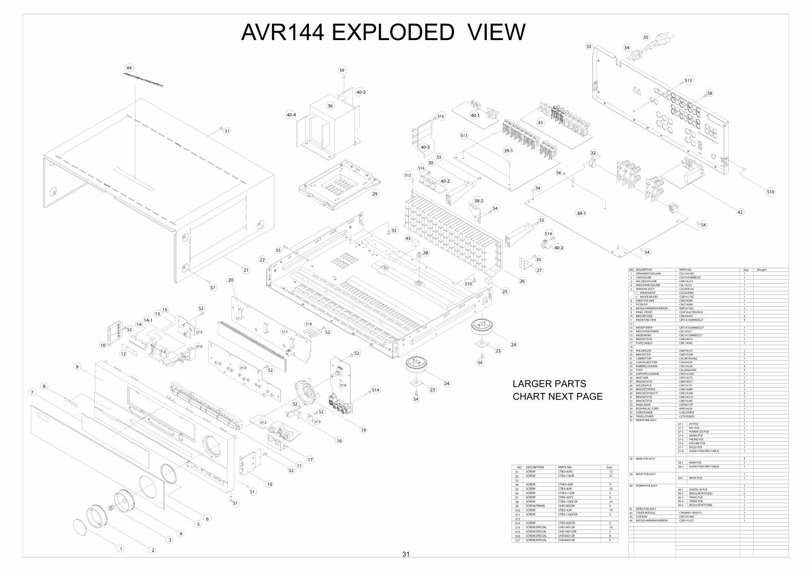
S7
S1
44
4
8
9
10
11
25
26
2721
28
29
36
30
32
34
35
22
S1
S2
S10
S5
S5
S9
S5
S4
S4
S4
S4
S6 x2
S11
S10
S8
S12
42
19
43
2
3
5
7
33
S1
1
6
38-1
39-1
37-2
S2
S14
17
S13
S2
S2
16
S5
37-1
41
16 BRACKET,PCB CMK2A010
BRACKET,PCB(H/T)
SUPPORT,CUSHION
FRONT PAB ASS'Y
BUSHING,AC CORD
29 BRACKET,TRANS
3637
30313233
3534
TRANS,POWER
PANEL,REARBRACKET,PCB
CORD,POWER
23242526
2827
17181920
2221
HOLDER,PCBBRACKET,PCBHEAT SINK
RUBBER,CUSHIONFOOT
PLATE,SHIELD
BRACKET,FIPHOLDER,LED
CHASSIS,BOTTOMCABINET,TOP
CMD1A487
CKF8A319Y
COP11910I
CJA523FBYAKHR1A028
CMD1A387
CMD1A398
CMY1A273
CUA2A229
CKL2A063H43
CKC4B145S46ZCMD1A209
CHE1A170CMD1A417
CHG1A104Z
CHG1A329
CMC1A302
CMH1A215
INDICATOR,VOLUME
BDAGE,HARMAN/KARDON
INDICATOR,POWER
3
10111213
1514
76
54
98
KNOB,MOMS
KNOB,POWER
KNOB,FUNCTION
FILTER,FIP
WINDOW ASS'Y
BRACKET,SIDEPANEL,FRONT
NO
21
HOLDER,VOLUMECAP,VOLUME
DESCRIPTION
CGL1A222CGUAVR144
CGW1A427RDZH43
CBC1A158MBZG27
CBT1A1026MMZG27
CBT1A1028MBZG27CMD2A443
KGB1A158ZCMZ1A088
CGL1A221
CGX1A338MBC63
PARTS NO.
CMH1A214
1
1
11
21
2
11
1144
22
3
1
1
11
1
1
11
11
11
1
21
Q,ty
11
37-137-237-337-437-537-637-737-8
FIP PCBKEY PCBPOWER LED PCBMOMS PCBPHONE PCBVOLUME PCBRS232 PCBGUIDE PCB(CARD CABLE)
38 MAIN PCB ASS'Y COP11911I 1
38-1 MAIN PCB
11
111
1
11
11
39 INPUT PCB ASS'Y COP11931I 1
39-1 INPUT PCB 1
POWER PCB ASS'Y40 COP11916I 1
40-1 DIGITAL IN PCB 1
BADGE,MODEL
BADGE,HARMAN/KARDON CGB1A152Z
CGB1A174Z
ORNAMENT,VOLUME CGU1A318Z 1
CHG1A160ZCUSHION
WINDOW,FIP CGU2A399Z12
11
CMZ2A090SHEET,VOLUME 1
BRACKET,PCB CMD1A570 1
Weright
VIDEO PCB ASS'Y41 COP11917I 1TUNER MODULE42 1
4344 1
1
40-4
40-3
40-1
37-6
37-5
2324
2324
S4
S4
S5
S2
S1
S12S13S14
S9
S11S10
S7S8
S6S5S4
S2S3
NO13CTB3+8JFCSCREW
SCREWSCREW,SPECIAL
CTB3+8JFZRCHD1A012R
SCREW
SCREW,TRANSSCREW
SCREWSCREW
SCREWSCREWSCREW
SCREW
CTB4+6FFC
CTB3+16GFZRCTB3+6JR
CTB3+10GFZRCHD1A023R
CTB3+10GR
CTW3+12JRCTB3+8JRCTW3+8JR
316
4
219
622
3109
31
DESCRIPTION PARTS NO. Q,ty
S16S17
S15SCREW,SPECIALSCREW,SPECIAL
CHD3A012RCHD4A012R
CHD1A012ZR65
2SCREW,SPECIAL
40-2 REGULATOR PCB(A) 5
40-3 TRANS PCB 1
40-4 TRANS PCB 1
40-5 REGULATOR PCB(B) 1
38-2 GUIDE PCB(CARD CABLE) 1
CNVM9011MS071L
CLT5U026ZU
37-410
S2
S2
14
1315
37-3
12
14-1
37-9
40-2
S14
40-5
S16
S16
S2
37-8
38-2
20
40-2
AVR144 EXPLODED VIEW
LARGER PARTSCHART NEXT PAGE
31
JRico
Rectangle
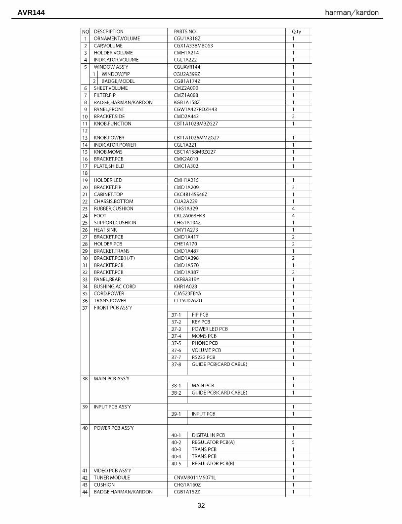
32
AVR144 harman/kardon
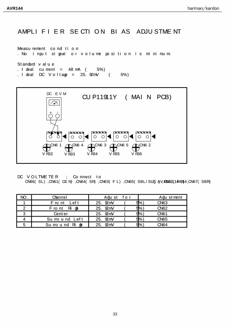
AMPLIFIER SECTION BIAS ADJUSTMENT
Measurement condition.No input signal or volume position is minimum.
Standard value.Ideal current = 48mA (± 5%).Ideal DC Voltage = 25.92mV (± 5%)
CUP11911Y (MAIN PCB)
DC VOLTMETER ; Connect to CN66(SL),CN61(CEN),CN64(SR),CN63(FL),CN65(SBL/SL(AVR132,144,145)),CN62(FR),CN67(SBR)
CN61
CN65
Adjust for Adjustment
25.92mV (± 5%)
CN64
25.92mV (± 5%)
25.92mV (± 5%)
25.92mV (± 5%)
25.92mV (± 5%)
CN63
CN62
Channel
Front Left
Front Right
Center
Surround Left
Surround Right
4
5
NO.
1
2
3
CN61
VR32
CN64
VR33
CN63
VR34
CN65
VR35
CN62
VR36
+ -
DC EVM
33
AVR144 harman/kardon
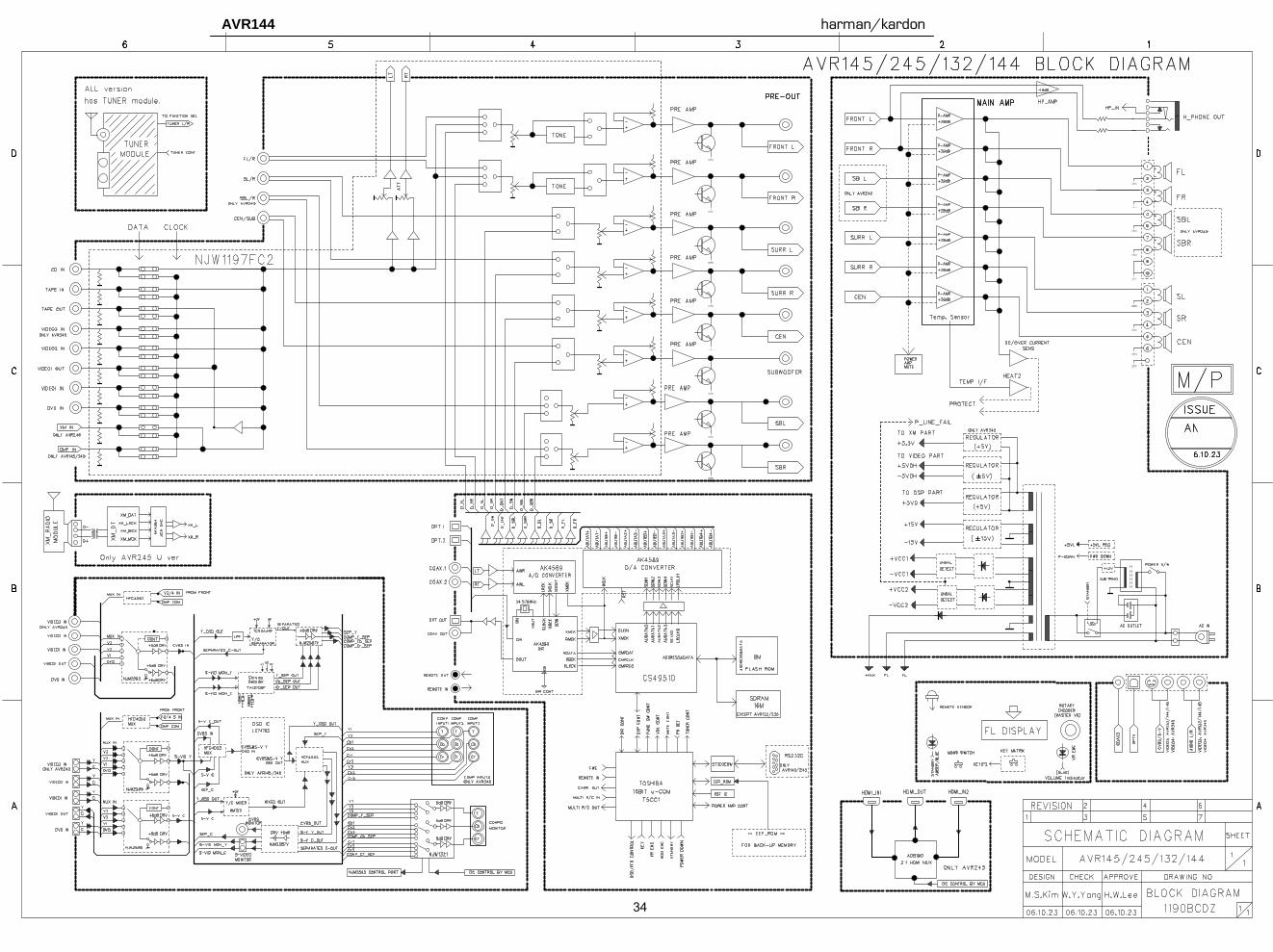
34
AVR144 harman/kardon
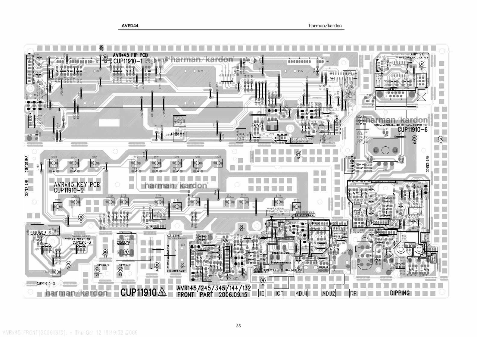
35
AVR144 harman/kardon
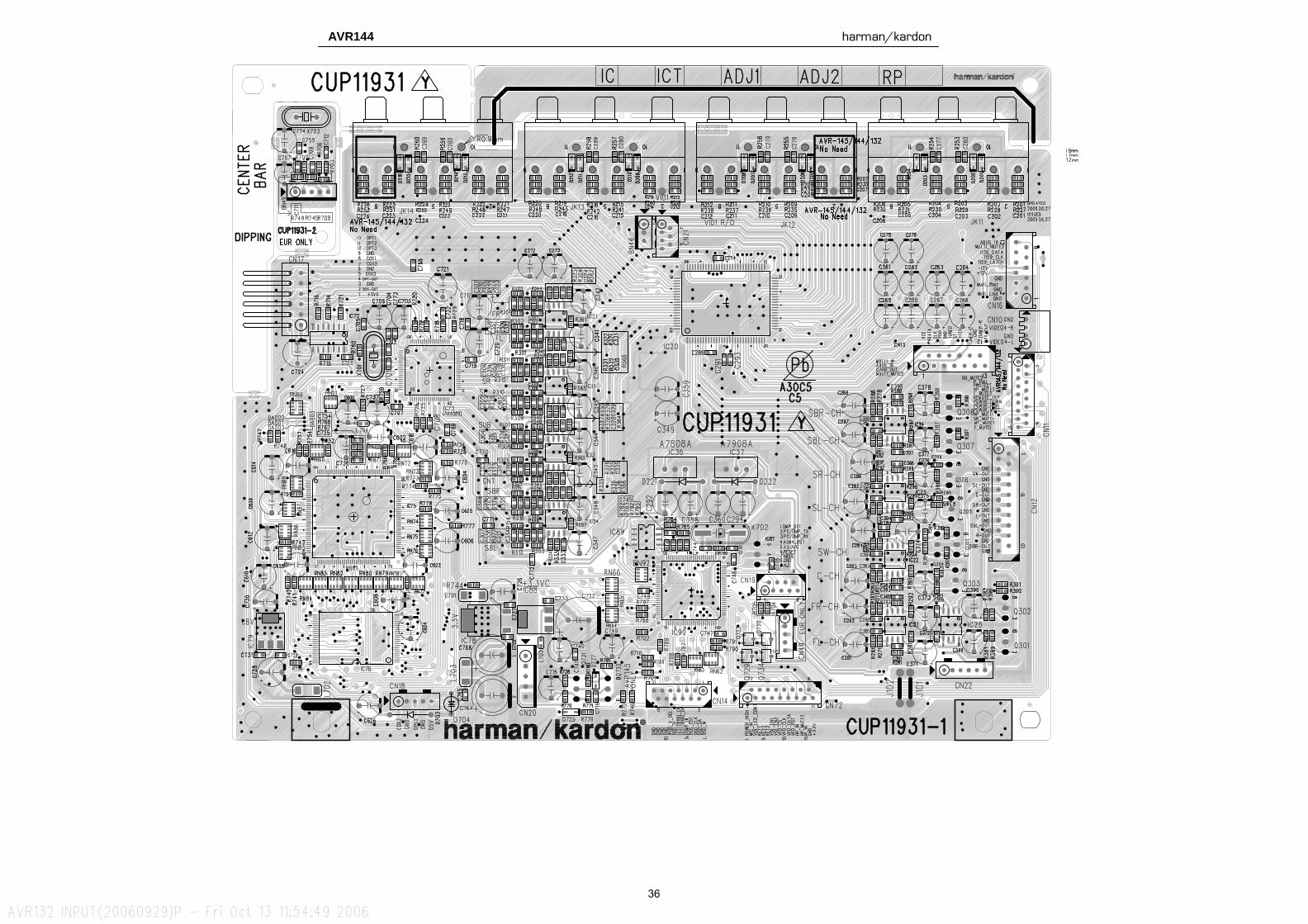
36
AVR144 harman/kardon
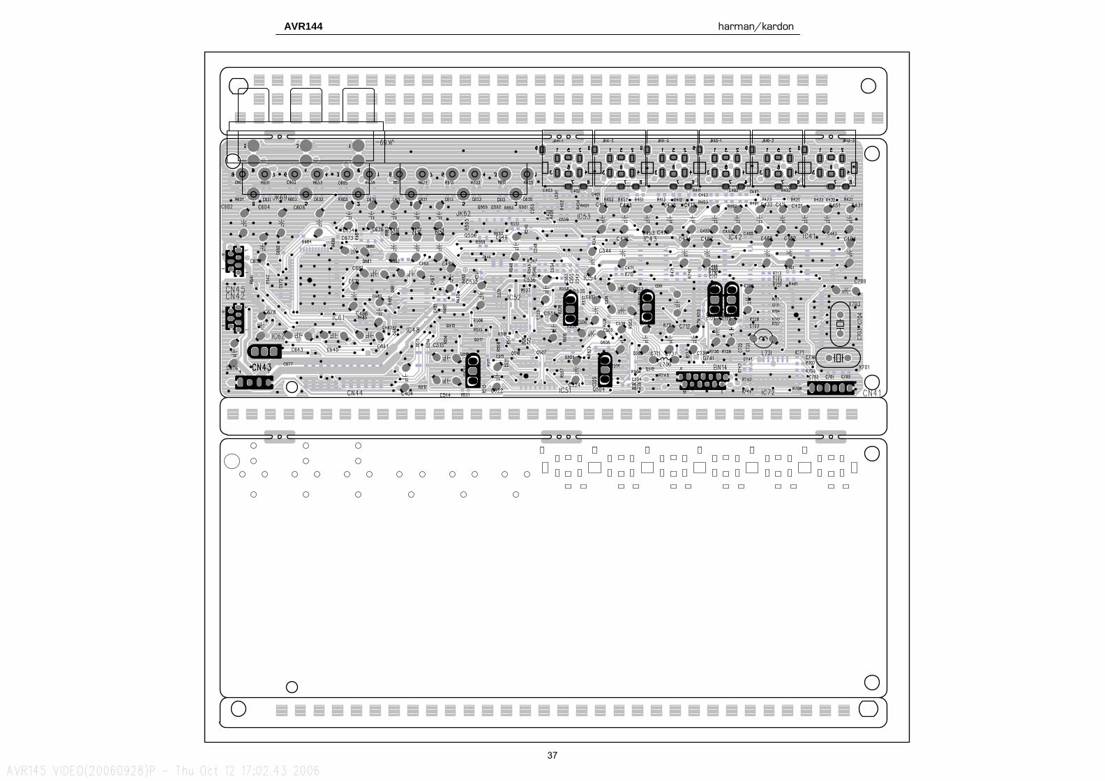
37
AVR144 harman/kardon

38
AVR144 harman/kardon

39
AVR144 harman/kardon

40
AVR144 harman/kardon
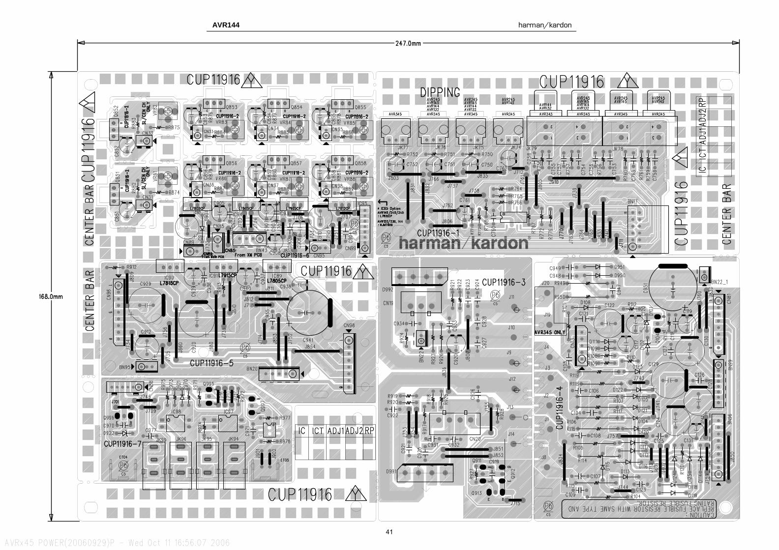
41
AVR144 harman/kardon
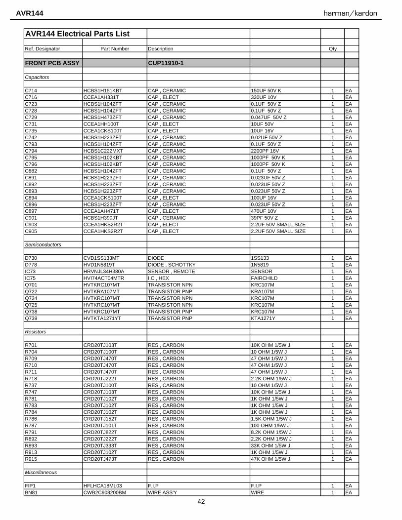
AVR144 Electrical Parts List
Ref. Designator Part Number Description Qty
FRONT PCB ASSY CUP11910-1
Capacitors
C714 HCBS1H151KBT CAP , CERAMIC 150UF 50V K 1 EAC716 CCEA1AH331T CAP , ELECT 330UF 10V 1 EAC723 HCBS1H104ZFT CAP , CERAMIC 0.1UF 50V Z 1 EAC728 HCBS1H104ZFT CAP , CERAMIC 0.1UF 50V Z 1 EAC729 HCBS1H473ZFT CAP , CERAMIC 0.047UF 50V Z 1 EAC731 CCEA1HH100T CAP , ELECT 10UF 50V 1 EAC735 CCEA1CKS100T CAP , ELECT 10UF 16V 1 EAC742 HCBS1H223ZFT CAP , CERAMIC 0.02UF 50V Z 1 EAC793 HCBS1H104ZFT CAP , CERAMIC 0.1UF 50V Z 1 EAC794 HCBS1C222MXT CAP , CERAMIC 2200PF 16V 1 EAC795 HCBS1H102KBT CAP , CERAMIC 1000PF 50V K 1 EAC796 HCBS1H102KBT CAP , CERAMIC 1000PF 50V K 1 EAC882 HCBS1H104ZFT CAP , CERAMIC 0.1UF 50V Z 1 EAC891 HCBS1H223ZFT CAP , CERAMIC 0.023UF 50V Z 1 EAC892 HCBS1H223ZFT CAP , CERAMIC 0.023UF 50V Z 1 EAC893 HCBS1H223ZFT CAP , CERAMIC 0.023UF 50V Z 1 EAC894 CCEA1CKS100T CAP , ELECT 100UF 16V 1 EAC896 HCBS1H223ZFT CAP , CERAMIC 0.023UF 50V Z 1 EAC897 CCEA1AH471T CAP , ELECT 470UF 10V 1 EAC901 HCBS1H390JT CAP , CERAMIC 39PF 50V Z 1 EAC903 CCEA1HKS2R2T CAP , ELECT 2.2UF 50V SMALL SIZE 1 EAC905 CCEA1HKS2R2T CAP , ELECT 2.2UF 50V SMALL SIZE 1 EA
Semiconductors
D730 CVD1SS133MT DIODE 1SS133 1 EAD778 HVD1N5819T DIODE , SCHOTTKY 1N5819 1 EAIC73 HRVNJL34H380A SENSOR , REMOTE SENSOR 1 EAIC75 HVI74ACT04MTR I.C , HEX FAIRCHILD 1 EAQ701 HVTKRC107MT TRANSISTOR NPN KRC107M 1 EAQ722 HVTKRA107MT TRANSISTOR PNP KRA107M 1 EAQ724 HVTKRC107MT TRANSISTOR NPN KRC107M 1 EAQ725 HVTKRC107MT TRANSISTOR NPN KRC107M 1 EAQ738 HVTKRC107MT TRANSISTOR PNP KRC107M 1 EAQ739 HVTKTA1271YT TRANSISTOR PNP KTA1271Y 1 EA
Resistors
R701 CRD20TJ103T RES , CARBON 10K OHM 1/5W J 1 EAR704 CRD20TJ100T RES , CARBON 10 OHM 1/5W J 1 EAR709 CRD20TJ470T RES , CARBON 47 OHM 1/5W J 1 EAR710 CRD20TJ470T RES , CARBON 47 OHM 1/5W J 1 EAR711 CRD20TJ470T RES , CARBON 47 OHM 1/5W J 1 EAR718 CRD20TJ222T RES , CARBON 2.2K OHM 1/5W J 1 EAR737 CRD20TJ100T RES , CARBON 10 OHM 1/5W J 1 EAR747 CRD20TJ103T RES , CARBON 10K OHM 1/5W J 1 EAR781 CRD20TJ102T RES , CARBON 1K OHM 1/5W J 1 EAR783 CRD20TJ102T RES , CARBON 1K OHM 1/5W J 1 EAR784 CRD20TJ102T RES , CARBON 1K OHM 1/5W J 1 EAR786 CRD20TJ152T RES , CARBON 1.5K OHM 1/5W J 1 EAR787 CRD20TJ101T RES , CARBON 100 OHM 1/5W J 1 EAR791 CRD20TJ822T RES , CARBON 8.2K OHM 1/5W J 1 EAR892 CRD20TJ222T RES , CARBON 2.2K OHM 1/5W J 1 EAR893 CRD20TJ333T RES , CARBON 33K OHM 1/5W J 1 EAR913 CRD20TJ102T RES , CARBON 1K OHM 1/5W J 1 EAR915 CRD20TJ473T RES , CARBON 47K OHM 1/5W J 1 EA
Miscellaneous
FIP1 HFLHCA18ML03 F.I.P F.I.P 1 EABN81 CWB2C908200BM WIRE ASS'Y WIRE 1 EA
42
AVR144 harman/kardon

Ref. Designator Part Number Description Qty
FRONT PCB ASSY CUP11910-1
BN84 CWB2B905080EN WIRE ASS'Y WIRE 1 EABN85 CWB2B902100EW WIRE ASS'Y ( ANGLE ) WIRE 1 EABN88 CWB2B904100EN WIRE ASS'Y WIRE 1 EA
CMC3A111 PLATE , EARTH PLATE 1 EAL702 HLQ02C100KT COIL , AXAIL COIL 1 EACN72 CJP17GA193ZY WAFER, CARD CABLE (SMD) WAFER 1 EACN89 CJP04GB46ZY WAFER WAFER 1 EA
PCB , FRONT STAND BY CUP11910-3
CN88 CJP04GB46ZY WAFER WAFER 1 EAR824 CRD20TJ221T RES , CARBON 220 OHM 1/5W J 1 EAR825 CRD20TJ681T RES , CARBON 680 OHM 1/5W J 1 EAR828 CRD20TJ221T RES , CARBON 220 OHM 1/5W J 1 EAR829 CRD20TJ681T RES , CARBON 680 OHM 1/5W J 1 EAS701 HST1A020ZT SW , TACT 1A020 1 EAD723 CVD50BOBBWGA L.E.D , 2 COLOR (ORG , BLUE) L.E.D 1 EAD727 CVD50BOBBWGA L.E.D , 2 COLOR (ORG , BLUE) L.E.D 1 EA
PCB , FRONT POWER (MOMS) SW CUP11910-4
CN86 CJP02GA89ZM WAFER WAFER 1 EASW1 CSH1A008ZV SW , PUSH (MOMS) MOMS SWITCH 1 EA
PCB , FRONT PANEL KEY CUP11910-2
Capacitors
C719 HCBS1H102KBT CAP , CERAMIC 1000PF 50V K 1 EAC720 HCBS1H102KBT CAP , CERAMIC 1000PF 50V K 1 EAC721 HCBS1H102KBT CAP , CERAMIC 1000PF 50V K 1 EA
Resistors
R753 CRD20TF1001T RES , CARBON 1K /1/5W /F 1 EAR754 CRD20TF1501T RES , CARBON 1.5K /1/5W /F 1 EAR755 CRD20TF1801T RES , CARBON 1.8K /1/5W /F 1 EAR756 CRD20TF2701T RES , CARBON 2.7K /1/5W/F 1 EAR757 CRD20TF3301T RES ,CARBON 3.3K /1/5W/F 1 EAR758 CRD20TF5601T RES ,CARBON(5.6K/F) 5.6K/1/5W/F 1 EAR759 CRD20TF1001T RES , CARBON 1K /1/5W /F 1 EAR760 CRD20TF1501T RES , CARBON 1.5K /1/5W /F 1 EAR761 CRD20TF1801T RES , CARBON 1.8K /1/5W /F 1 EAR762 CRD20TF2701T RES , CARBON 2.7K /1/5W/F 1 EAR763 CRD20TF3301T RES ,CARBON 3.3K /1/5W/F 1 EAR764 CRD20TF5601T RES ,CARBON(5.6K/F) 5.6K/1/5W/F 1 EAR765 CRD20TF7501T RES , CARBON (7.5K/F) 7.5K/1/5W/F 1 EAR766 CRD20TF1001T RES , CARBON 1K /1/5W /F 1 EAR767 CRD20TF1501T RES , CARBON 1.5K /1/5W /F 1 EAR768 CRD20TF1801T RES , CARBON 1.8K /1/5W /F 1 EAR769 CRD20TF2701T RES , CARBON 2.7K /1/5W/F 1 EA
Miscellaneous
S701 HST1A020ZT SW , TACT 1A020 1 EAS702 HST1A020ZT SW , TACT 1A020 1 EAS703 HST1A020ZT SW , TACT 1A020 1 EAS704 HST1A020ZT SW , TACT 1A020 1 EAS705 HST1A020ZT SW , TACT 1A020 1 EAS706 HST1A020ZT SW , TACT 1A020 1 EAS707 HST1A020ZT SW , TACT 1A020 1 EAS711 HST1A020ZT SW , TACT 1A020 1 EAS712 HST1A020ZT SW , TACT 1A020 1 EAS713 HST1A020ZT SW , TACT 1A020 1 EA
43
AVR144 harman/kardon

Ref. Designator Part Number Description Qty
PCB , FRONT PANEL KEY CUP11910-2
S714 HST1A020ZT SW , TACT 1A020 1 EAS715 HST1A020ZT SW , TACT 1A020 1 EABN89 CWB2B904100EN WIRE ASS'Y WIRE 1 EA
PCB , VR JACK CUP11910-6
Capacitors
C805 HCBS1H223ZFT CAP , CERAMIC 0.022UF 50V Z 1 EAC806 HCBS1H223ZFT CAP , CERAMIC 0.022UF 50V Z 1 EAC841 CCEA1HH100T CAP , ELECT 10UF 50V 1 EAC842 CCEA1HH100T CAP , ELECT 10UF 50V 1 EAC843 CCEA1HH100T CAP , ELECT 10UF 50V 1 EAC855 HCBS1H101KBT CAP , CERAMIC 100PF 50V K 1 EAC856 HCBS1H101KBT CAP , CERAMIC 100PF 50V K 1 EAC857 HCBS1H104ZFT CAP , CERAMIC 0.1UF 50V Z 1 EAC862 HCBS1H101KBT CAP , CERAMIC 100PF 50V K 1 EAC863 HCBS1H101KBT CAP , CERAMIC 100PF 50V K 1 EAC874 HCBS1H101KBT CAP , CERAMIC 100PF 50V K 1 EA
Semiconductors
D774 CVD1SS133MT DIODE 1SS133 1 EAD701 CVD52CSBBCEAB2 BLUE L.E.D L.E.D 1 EAD703 CVD52CSBBCEAB2 BLUE L.E.D L.E.D 1 EAD705 CVD52CSBBCEAB2 BLUE L.E.D L.E.D 1 EA
Resistors
R705 CRD20TJ820T RES , CARBON 82 OHM 1/5W J 1 EAR706 CRD20TJ820T RES , CARBON 82 OHM 1/5W J 1 EAR708 CRD20TJ820T RES , CARBON 82 OHM 1/5W J 1 EAR864 CRD20TJ272T RES , CARBON 2.7K OHM 1/5W J 1 EAR865 CRD20TJ101T RES , CARBON 100 OHM 1/5W J 1 EAR866 CRD20TJ272T RES , CARBON 2.7K OHM 1/5W J 1 EAR871 CRD20TJ104T RES , CARBON 100K OHM 1/5W J 1 EAR872 CRD20TJ104T RES , CARBON 100K OHM 1/5W J 1 EAR873 CRD20TJ471T RES , CARBON 470 OHM 1/5W J 1 EAR874 CRD20TJ471T RES , CARBON 470 OHM 1/5W J 1 EAR876 CRD20TJ750T RES , CARBON 75 OHM 1/5W J 1 EAR877 CRD20TJ750T RES , CARBON 75 OHM 1/5W J 1 EAR878 CRD20TJ750T RES , CARBON 75 OHM 1/5W J 1 EAR881 C3A206 WIRE , COPPER SN95/PB5 , 0.6R882 C3A206 WIRE , COPPER SN95/PB5 , 0.6VR74 CSR2A037Z ENCODER ENCODER 1 EA
Miscellaneous
CN84 CJP05GB46ZY WAFER WAFER 1 EABN10 CWZAVR230BN10 WIRE ASS'Y (SHIELD) WIRE 1 EABN41 CWZAVR130BN41 WIRE ASS'Y (SHIELD) WIRE 1 EAJK85 CJJ9M003Z JACK , S-VIDEO S-VIDEO JACK 1 EAJK86 CJJ4S023Y JACK , BOARD BOARD 1 EAJW84 CWE8202110RV WIRE ASS'Y WIRE 1 EA
PCB , PHONE JACK CUP11910-5
Capacitors
C807 HCBS1H104ZFT CAP , CERAMIC 0.1UF 50V Z 1 EAC808 HCBS1H181KBT CAP , CERAMIC 180PF 50V Z 1 EAC809 CCEA1AH471T CAP , ELECT 470UF 10V 1 EAC812 HCBS1H104ZFT CAP , CERAMIC 0.1UF 50V Z 1 EAC817 HCBS1H100JCT CAP , CERAMIC 10PF 50V 1 EAC850 HCBS1H471KBT CAP , CERAMIC 470PF 50V 1 EA
44
AVR144 harman/kardon

Ref. Designator Part Number Description Qty
PCB , PHONE JACK CUP11910-5
C851 HCBS1H471KBT CAP , CERAMIC 470PF 50V 1 EAC852 HCBS1H104ZFT CAP , CERAMIC 0.1UF 50V Z 1 EAC866 CCEA1HKS100T CAP , ELECT 10UF 50V 1 EAC867 CCEA1HKS100T CAP , ELECT 10UF 50V 1 EAC868 CCEA1EKS470T CAP , ELECT 47UF 25V 1 EAC869 CCEA1EKS470T CAP , ELECT 47UF 25V 1 EAC870 HCBS1H681KBT CAP , CERAMIC 680PF 50V K 1 EAC871 HCBS1H681KBT CAP , CERAMIC 680PF 50V K 1 EAC872 CCEA1CH331T CAP , ELECT 330UF 16V 1 EAC873 CCEA1CH331T CAP , ELECT 330UF 16V 1 EAC889 HCBS1H104ZFT CAP , CERAMIC 0.1UF 50V Z 1 EA
Semiconductors
D784 CVD1SS133MT DIODE 1SS133 1 EAD785 CVD1SS133MT DIODE 1SS133 1 EAQ734 HVTKTC2874BT TRANSISTOR , MUTE NPN KTC2874B 1 EAQ735 HVTKTC2874BT TRANSISTOR , MUTE NPN KTC2874B 1 EAQ736 HVTKTC2874BT TRANSISTOR , MUTE NPN KTC2874B 1 EAQ737 HVTKTC2874BT TRANSISTOR , MUTE NPN KTC2874B 1 EAIC76 HVI74HCU04AFNG I.C , INVERTER TOSHIBA 1 EAIC86 HVINJM4556AL I.C , HEADPHONE JRC 1 EA
Resistors
R456 C3A206 WIRE , COPPER SN95/PB5 , 0.6R457 C3A206 WIRE , COPPER SN95/PB5 , 0.6R805 CRD20TJ104T RES , CARBON 100K OHM 1/5W J 1 EAR806 CRD20TJ472T RES , CARBON 4.7K OHM 1/5W J 1 EAR869 CRD20TJ750T RES , CARBON 75 OHM 1/5W J 1 EAR875 CRD20TJ103T RES , CARBON 10K OHM 1/5W J 1 EAR895 CRD20TJ101T RES , CARBON 100 OHM 1/5W J 1 EAR896 CRD20TJ101T RES , CARBON 100 OHM 1/5W J 1 EAR897 CRD20TJ101T RES , CARBON 100 OHM 1/5W J 1 EAR898 CRD20TJ101T RES , CARBON 100 OHM 1/5W J 1 EAR899 CRD20TJ104T RES , CARBON 100K OHM 1/5W J 1 EAR900 CRD20TJ104T RES , CARBON 100K OHM 1/5W J 1 EAR901 CRD20TJ152T RES , CARBON 1.5K OHM 1/5W J 1 EAR902 CRD20TJ152T RES , CARBON 1.5K OHM 1/5W J 1 EAR903 CRD20TJ102T RES , CARBON 1K OHM 1/5W J 1 EAR904 CRD20TJ102T RES , CARBON 1K OHM 1/5W J 1 EAR905 CRD20TJ104T RES , CARBON 100K OHM 1/5W J 1 EAR906 CRD20TJ104T RES , CARBON 100K OHM 1/5W J 1 EAR907 CRD20TJ472T RES , CARBON 4.7K OHM 1/5W J 1 EAR908 CRD20TJ472T RES , CARBON 4.7K OHM 1/5W J 1 EAR909 CRD20TJ221T RES , CARBON 220 OHM 1/5W J 1 EAR910 CRD20TJ221T RES , CARBON 220 OHM 1/5W J 1 EAR911 CRD20TJ221T RES , CARBON 220 OHM 1/5W J 1 EAR912 CRD20TJ221T RES , CARBON 220 OHM 1/5W J 1 EAR918 CRD20TJ472T RES , CARBON 4.7K OHM 1/5W J 1 EAR919 CRD20TJ472T RES , CARBON 4.7K OHM 1/5W J 1 EA
Miscellaneous
CN85 CJP02GA19ZY WAFER, 2PIN WAFER 1 EABN18 CWZAVR125BN18 WIRE ASS'Y (SHIELD) WIRE 1 EABN22 CWZAVR145BN22 WIRE ASS'Y (SHIELD) WIRE 1 EAJK81 CJJ4M043Y JACK,BOARD BOARD 1 EAJK82 HJSTORX177L MODULE , OPTICAL(RX) OPTICAL JACK 1 EAJK83 CJJ2E026Z JACK , HEADPHONE(SILVER PLATE) HDEAPHONE JACK 1 EAJW82 CWE8202300RV WIRE ASS'Y WIRE 1 EAJW83 CWE8202150RV WIRE ASS'Y WIRE 1 EA
45
AVR144 harman/kardon
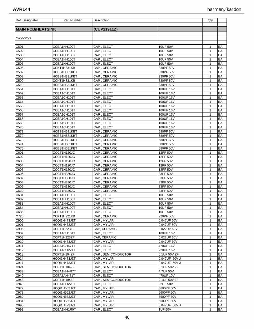
Ref. Designator Part Number Description Qty
MAIN PCB/HEATSINK (CUP11911Z)
Capacitors
C501 CCEA1HH100T CAP , ELECT 10UF 50V 1 EAC502 CCEA1HH100T CAP , ELECT 10UF 50V 1 EAC503 CCEA1HH100T CAP , ELECT 10UF 50V 1 EAC504 CCEA1HH100T CAP , ELECT 10UF 50V 1 EAC505 CCEA1HH100T CAP , ELECT 10UF 50V 1 EAC506 CCKT1H331KB CAP , CERAMIC 330PF 50V 1 EAC507 HCBS1H331KBT CAP , CERAMIC 330PF 50V 1 EAC508 HCBS1H331KBT CAP , CERAMIC 330PF 50V 1 EAC509 CCKT1H331KB CAP , CERAMIC 330PF 50V 1 EAC510 HCBS1H331KBT CAP , CERAMIC 330PF 50V 1 EAC561 CCEA1CH101T CAP , ELECT 100UF 16V 1 EAC562 CCEA1CH101T CAP , ELECT 100UF 16V 1 EAC563 CCEA1CH101T CAP , ELECT 100UF 16V 1 EAC564 CCEA1CH101T CAP , ELECT 100UF 16V 1 EAC565 CCEA1CH101T CAP , ELECT 100UF 16V 1 EAC566 CCEA1CH101T CAP , ELECT 100UF 16V 1 EAC567 CCEA1CH101T CAP , ELECT 100UF 16V 1 EAC568 CCEA1CH101T CAP , ELECT 100UF 16V 1 EAC569 CCEA1CH101T CAP , ELECT 100UF 16V 1 EAC570 CCEA1CH101T CAP , ELECT 100UF 16V 1 EAC571 HCBS1H681KBT CAP , CERAMIC 680PF 50V 1 EAC572 HCBS1H681KBT CAP , CERAMIC 680PF 50V 1 EAC573 HCBS1H681KBT CAP , CERAMIC 680PF 50V 1 EAC574 HCBS1H681KBT CAP , CERAMIC 680PF 50V 1 EAC575 HCBS1H681KBT CAP , CERAMIC 680PF 50V 1 EAC601 CCCT1H120JC CAP , CERAMIC 12PF 50V 1 EAC602 CCCT1H120JC CAP , CERAMIC 12PF 50V 1 EAC603 CCCT1H120JC CAP , CERAMIC 12PF 50V 1 EAC604 CCCT1H120JC CAP , CERAMIC 12PF 50V 1 EAC605 CCCT1H120JC CAP , CERAMIC 12PF 50V 1 EAC606 CCCT1H330JC CAP , CERAMIC 33PF 50V 1 EAC607 CCCT1H330JC CAP , CERAMIC 33PF 50V 1 EAC608 CCCT1H330JC CAP , CERAMIC 33PF 50V 1 EAC609 CCCT1H330JC CAP , CERAMIC 33PF 50V 1 EAC610 CCCT1H330JC CAP , CERAMIC 33PF 50V 1 EAC681 CCEA1HH100T CAP , ELECT 10UF 50V 1 EAC682 CCEA1HH100T CAP , ELECT 10UF 50V 1 EAC683 CCEA1HH100T CAP , ELECT 10UF 50V 1 EAC684 CCEA1HH100T CAP , ELECT 10UF 50V 1 EAC685 CCEA1HH100T CAP , ELECT 10UF 50V 1 EAC726 CCKT1H221KB CAP , CERAMIC 220PF 50V 1 EAC900 HCQI1H473JZT CAP , MYLAR 0.047UF 50V 1 EAC901 HCQI1H473JZT CAP , MYLAR 0.047UF 50V 1 EAC905 CCFT1H223ZF CAP, CERAMIC 0.022UP 50V 1 EAC907 CCEA1CH101T CAP , ELECT 100UF 16V 1 EAC908 CCFT1H223ZF CAP, CERAMIC 0.022UP 50V 1 EAC910 HCQI1H473JZT CAP , MYLAR 0.047UF 50V 1 EAC911 CCEA1CH471T CAP , ELECT 470UF 16V 1 EAC912 CCEA1CH221T CAP , ELECT 220UF 16V 1 EAC913 CCFT1H104ZF CAP , SEMICONDUCTOR 0.1UF 50V ZF 1 EAC914 HCQI1H473JZT CAP , MYLAR 0.047UF 50V J 1 EAC917 HCQI1H473JZT CAP , MYLAR 0.047UF 50V J 1 EAC924 CCFT1H104ZF CAP , SEMICONDUCTOR 0.1UF 50V ZF 1 EAC939 CCEA1HH4R7T CAP , ELECT 4.7UF 50V 1 EAC940 CCEA1AH471T CAP , ELECT 470UF 10V 1 EAC948 CCFT1H104ZF CAP , SEMICONDUCTOR 0.1UF 50V ZF 1 EAC949 CCEA1HH220T CAP , ELECT 22UF 50V 1 EAC972 HCQI1H562JZT CAP , MYLAR 5600PF 50V 1 EAC973 HCQI1H562JZT CAP , MYLAR 5600PF 50V 1 EAC980 HCQI1H562JZT CAP , MYLAR 5600PF 50V 1 EAC981 HCQI1H562JZT CAP , MYLAR 5600PF 50V 1 EAC990 HCQI1H473JZT CAP , MYLAR 0.047UF 50V J 1 EAC991 CCEA1HH1R0T CAP , ELECT 1UF 50V 1 EA
46
AVR144 harman/kardon

Ref. Designator Part Number Description Qty
MAIN PCB/HEATSINK (CUP11911Z)
C992 HCQI1H473JZT CAP , MYLAR 0.047UF 50V J 1 EAC993 HCQI1H473JZT CAP , MYLAR 0.047UF 50V J 1 EAC995 HCQI1H473JZT CAP , MYLAR 0.047UF 50V J 1 EAC997 HCQI1H473JZT CAP , MYLAR 0.047UF 50V J 1 EAC999 CCFT1H223ZF CAP, CERAMIC 0.022UP 50V 1 EAC631 CCEA1JH101E CAP , ELECT 100UF 63V 1 EAC632 CCEA1JH101E CAP , ELECT 100UF 63V 1 EAC633 CCEA1JH101E CAP , ELECT 100UF 63V 1 EAC634 CCEA1JH101E CAP , ELECT 100UF 63V 1 EAC635 CCEA1JH101E CAP , ELECT 100UF 63V 1 EAC636 CCEA1JH101E CAP , ELECT 100UF 63V 1 EAC637 CCEA1JH101E CAP , ELECT 100UF 63V 1 EAC638 CCEA1JH101E CAP , ELECT 100UF 63V 1 EAC639 CCEA1JH101E CAP , ELECT 100UF 63V 1 EAC640 CCEA1JH101E CAP , ELECT 100UF 63V 1 EAC902 CCET50VKL4682NK CAP , ELECT 6800UF/50V 1 EAC904 KCKDKS472ME CAP , CERAMIC(X1/Y2/SC) 0.0047UF/2.5KV 1 EAC906 CCEA1EH102E CAP , ELECT 1000UF 25V 1 EAC909 CCET50VKL4682NK CAP , ELECT 6800UF/50V 1 EAC915 CCET50VKL4682NK CAP , ELECT 6800UF/50V 1 EAC916 CCET50VKL4682NK CAP , ELECT 6800UF/50V 1 EA
Semiconductors
D501 CVD1SS133MT DIODE 1SS133 1 EAD502 CVD1SS133MT DIODE 1SS133 1 EAD503 CVD1SS133MT DIODE 1SS133 1 EAD504 CVD1SS133MT DIODE 1SS133 1 EAD505 CVD1SS133MT DIODE 1SS133 1 EAD581 CVD1SS133MT DIODE 1SS133 1 EAD582 CVD1SS133MT DIODE 1SS133 1 EAD583 CVD1SS133MT DIODE 1SS133 1 EAD584 CVD1SS133MT DIODE 1SS133 1 EAD585 CVD1SS133MT DIODE 1SS133 1 EAD901 CVD1N4003SRT RECT , DIODE 1N4003 1 EAD902 CVD1SS133MT DIODE 1SS133 1 EAD911 CVD1SS133MT DIODE 1SS133 1 EAD912 CVD1SS133MT DIODE 1SS133 1 EAD914 CVD1SS133MT DIODE 1SS133 1 EAD917 CVD1SS133MT DIODE 1SS133 1 EAD953 CVD1SS133MT DIODE 1SS133 1 EAD954 CVD1N4003SRT RECT , DIODE 1N4003 1 EAD955 CVD1N4003SRT RECT , DIODE 1N4003 1 EAD956 CVD1N4003SRT RECT , DIODE 1N4003 1 EAD957 CVD1N4003SRT RECT , DIODE 1N4003 1 EAD961 CVD1N4003ST RECT , DIODE 1N4003 1 EAD962 CVD1N4003SRT RECT , DIODE 1N4003 1 EAD963 CVD1N4003ST RECT , DIODE 1N4003 1 EAD973 CVD1SS133MT DIODE 1SS133 1 EAD974 CVD1SS133MT DIODE 1SS133 1 EAD979 HVDMTZJ6.2BT DIODE , ZENER MTZJ6.2B 1 EAD980 CVD1SS133MT DIODE 1SS133 1 EAQ501 HVTKTA1268GRT TRANSISTOR PNP KTA1268GR 1 EAQ502 HVTKTA1268GRT TRANSISTOR PNP KTA1268GR 1 EAQ503 HVTKTA1268GRT TRANSISTOR PNP KTA1268GR 1 EAQ504 HVTKTA1268GRT TRANSISTOR PNP KTA1268GR 1 EAQ505 HVTKTA1268GRT TRANSISTOR PNP KTA1268GR 1 EAQ511 HVTKTC3200GRT TRANSISTOR NPN KTC3200GR 1 EAQ512 HVTKTC3200GRT TRANSISTOR NPN KTC3200GR 1 EAQ513 HVTKTC3200GRT TRANSISTOR NPN KTC3200GR 1 EAQ514 HVTKTC3200GRT TRANSISTOR NPN KTC3200GR 1 EAQ515 HVTKTC3200GRT TRANSISTOR NPN KTC3200GR 1 EAQ516 HVTKTC3200GRT TRANSISTOR NPN KTC3200GR 1 EAQ517 HVTKTC3200GRT TRANSISTOR NPN KTC3200GR 1 EAQ518 HVTKTC3200GRT TRANSISTOR NPN KTC3200GR 1 EA
47
AVR144 harman/kardon
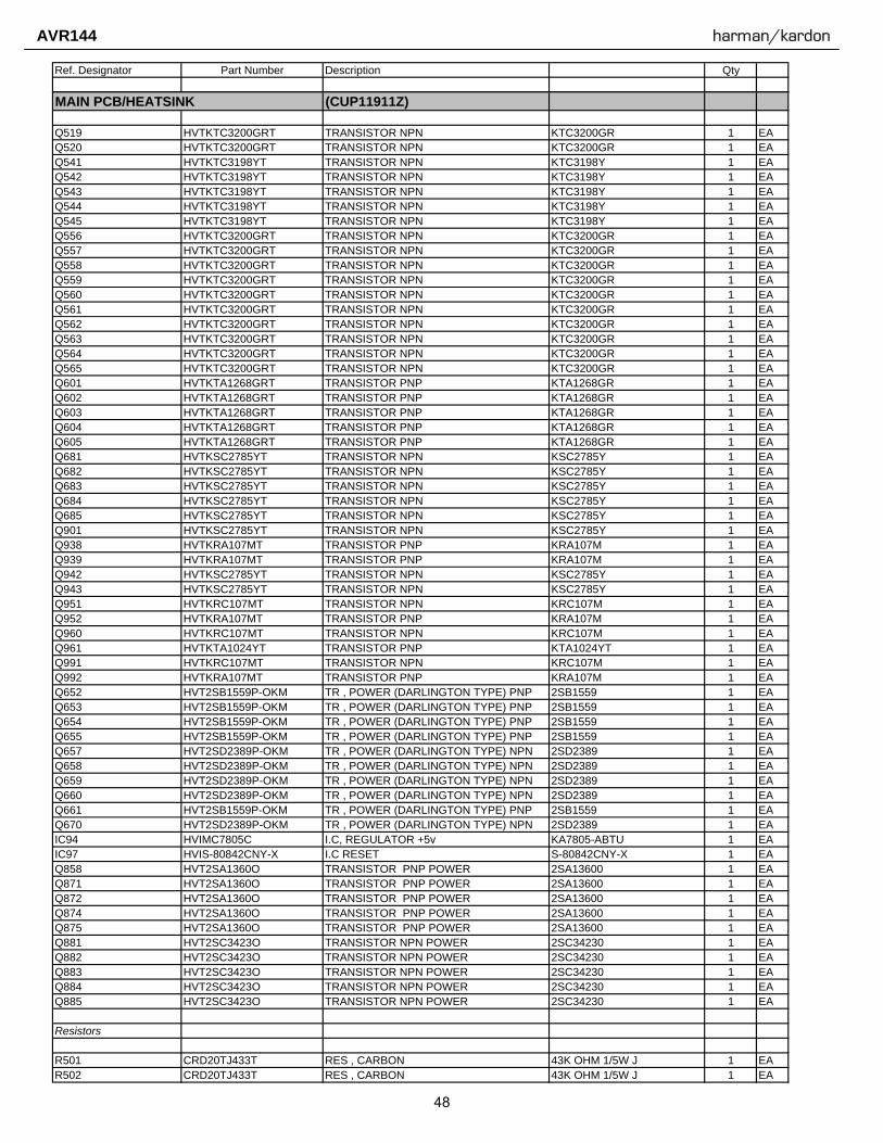
Ref. Designator Part Number Description Qty
MAIN PCB/HEATSINK (CUP11911Z)
Q519 HVTKTC3200GRT TRANSISTOR NPN KTC3200GR 1 EAQ520 HVTKTC3200GRT TRANSISTOR NPN KTC3200GR 1 EAQ541 HVTKTC3198YT TRANSISTOR NPN KTC3198Y 1 EAQ542 HVTKTC3198YT TRANSISTOR NPN KTC3198Y 1 EAQ543 HVTKTC3198YT TRANSISTOR NPN KTC3198Y 1 EAQ544 HVTKTC3198YT TRANSISTOR NPN KTC3198Y 1 EAQ545 HVTKTC3198YT TRANSISTOR NPN KTC3198Y 1 EAQ556 HVTKTC3200GRT TRANSISTOR NPN KTC3200GR 1 EAQ557 HVTKTC3200GRT TRANSISTOR NPN KTC3200GR 1 EAQ558 HVTKTC3200GRT TRANSISTOR NPN KTC3200GR 1 EAQ559 HVTKTC3200GRT TRANSISTOR NPN KTC3200GR 1 EAQ560 HVTKTC3200GRT TRANSISTOR NPN KTC3200GR 1 EAQ561 HVTKTC3200GRT TRANSISTOR NPN KTC3200GR 1 EAQ562 HVTKTC3200GRT TRANSISTOR NPN KTC3200GR 1 EAQ563 HVTKTC3200GRT TRANSISTOR NPN KTC3200GR 1 EAQ564 HVTKTC3200GRT TRANSISTOR NPN KTC3200GR 1 EAQ565 HVTKTC3200GRT TRANSISTOR NPN KTC3200GR 1 EAQ601 HVTKTA1268GRT TRANSISTOR PNP KTA1268GR 1 EAQ602 HVTKTA1268GRT TRANSISTOR PNP KTA1268GR 1 EAQ603 HVTKTA1268GRT TRANSISTOR PNP KTA1268GR 1 EAQ604 HVTKTA1268GRT TRANSISTOR PNP KTA1268GR 1 EAQ605 HVTKTA1268GRT TRANSISTOR PNP KTA1268GR 1 EAQ681 HVTKSC2785YT TRANSISTOR NPN KSC2785Y 1 EAQ682 HVTKSC2785YT TRANSISTOR NPN KSC2785Y 1 EAQ683 HVTKSC2785YT TRANSISTOR NPN KSC2785Y 1 EAQ684 HVTKSC2785YT TRANSISTOR NPN KSC2785Y 1 EAQ685 HVTKSC2785YT TRANSISTOR NPN KSC2785Y 1 EAQ901 HVTKSC2785YT TRANSISTOR NPN KSC2785Y 1 EAQ938 HVTKRA107MT TRANSISTOR PNP KRA107M 1 EAQ939 HVTKRA107MT TRANSISTOR PNP KRA107M 1 EAQ942 HVTKSC2785YT TRANSISTOR NPN KSC2785Y 1 EAQ943 HVTKSC2785YT TRANSISTOR NPN KSC2785Y 1 EAQ951 HVTKRC107MT TRANSISTOR NPN KRC107M 1 EAQ952 HVTKRA107MT TRANSISTOR PNP KRA107M 1 EAQ960 HVTKRC107MT TRANSISTOR NPN KRC107M 1 EAQ961 HVTKTA1024YT TRANSISTOR PNP KTA1024YT 1 EAQ991 HVTKRC107MT TRANSISTOR NPN KRC107M 1 EAQ992 HVTKRA107MT TRANSISTOR PNP KRA107M 1 EAQ652 HVT2SB1559P-OKM TR , POWER (DARLINGTON TYPE) PNP 2SB1559 1 EAQ653 HVT2SB1559P-OKM TR , POWER (DARLINGTON TYPE) PNP 2SB1559 1 EAQ654 HVT2SB1559P-OKM TR , POWER (DARLINGTON TYPE) PNP 2SB1559 1 EAQ655 HVT2SB1559P-OKM TR , POWER (DARLINGTON TYPE) PNP 2SB1559 1 EAQ657 HVT2SD2389P-OKM TR , POWER (DARLINGTON TYPE) NPN 2SD2389 1 EAQ658 HVT2SD2389P-OKM TR , POWER (DARLINGTON TYPE) NPN 2SD2389 1 EAQ659 HVT2SD2389P-OKM TR , POWER (DARLINGTON TYPE) NPN 2SD2389 1 EAQ660 HVT2SD2389P-OKM TR , POWER (DARLINGTON TYPE) NPN 2SD2389 1 EAQ661 HVT2SB1559P-OKM TR , POWER (DARLINGTON TYPE) PNP 2SB1559 1 EAQ670 HVT2SD2389P-OKM TR , POWER (DARLINGTON TYPE) NPN 2SD2389 1 EAIC94 HVIMC7805C I.C, REGULATOR +5v KA7805-ABTU 1 EAIC97 HVIS-80842CNY-X I.C RESET S-80842CNY-X 1 EAQ858 HVT2SA1360O TRANSISTOR PNP POWER 2SA13600 1 EAQ871 HVT2SA1360O TRANSISTOR PNP POWER 2SA13600 1 EAQ872 HVT2SA1360O TRANSISTOR PNP POWER 2SA13600 1 EAQ874 HVT2SA1360O TRANSISTOR PNP POWER 2SA13600 1 EAQ875 HVT2SA1360O TRANSISTOR PNP POWER 2SA13600 1 EAQ881 HVT2SC3423O TRANSISTOR NPN POWER 2SC34230 1 EAQ882 HVT2SC3423O TRANSISTOR NPN POWER 2SC34230 1 EAQ883 HVT2SC3423O TRANSISTOR NPN POWER 2SC34230 1 EAQ884 HVT2SC3423O TRANSISTOR NPN POWER 2SC34230 1 EAQ885 HVT2SC3423O TRANSISTOR NPN POWER 2SC34230 1 EA
Resistors
R501 CRD20TJ433T RES , CARBON 43K OHM 1/5W J 1 EAR502 CRD20TJ433T RES , CARBON 43K OHM 1/5W J 1 EA
48
AVR144 harman/kardon

Ref. Designator Part Number Description Qty
MAIN PCB/HEATSINK (CUP11911Z)
R503 CRD20TJ433T RES , CARBON 43K OHM 1/5W J 1 EAR504 CRD20TJ433T RES , CARBON 43K OHM 1/5W J 1 EAR505 CRD20TJ433T RES , CARBON 43K OHM 1/5W J 1 EAR506 CRD20TJ333T RES , CARBON 33K OHM 1/5W J 1 EAR507 CRD20TJ333T RES , CARBON 33K OHM 1/5W J 1 EAR508 CRD20TJ333T RES , CARBON 33K OHM 1/5W J 1 EAR509 CRD20TJ333T RES , CARBON 33K OHM 1/5W J 1 EAR510 CRD20TJ333T RES , CARBON 33K OHM 1/5W J 1 EAR511 CRD20TJ152T RES , CARBON 1.5K OHM 1/5W J 1 EAR512 CRD20TJ152T RES , CARBON 1.5K OHM 1/5W J 1 EAR513 CRD20TJ152T RES , CARBON 1.5K OHM 1/5W J 1 EAR514 CRD20TJ152T RES , CARBON 1.5K OHM 1/5W J 1 EAR515 CRD20TJ152T RES , CARBON 1.5K OHM 1/5W J 1 EAR516 CRD20TJ152T RES , CARBON 1.5K OHM 1/5W J 1 EAR517 CRD20TJ152T RES , CARBON 1.5K OHM 1/5W J 1 EAR518 CRD20TJ152T RES , CARBON 1.5K OHM 1/5W J 1 EAR519 CRD20TJ152T RES , CARBON 1.5K OHM 1/5W J 1 EAR520 CRD20TJ152T RES , CARBON 1.5K OHM 1/5W J 1 EAR521 CRD20TJ471T RES , CARBON 470 OHM 1/5W J 1 EAR522 CRD20TJ471T RES , CARBON 470 OHM 1/5W J 1 EAR523 CRD20TJ471T RES , CARBON 470 OHM 1/5W J 1 EAR524 CRD20TJ471T RES , CARBON 470 OHM 1/5W J 1 EAR525 CRD20TJ471T RES , CARBON 470 OHM 1/5W J 1 EAR531 CRD20TJ221T RES , CARBON 220 OHM 1/5W J 1 EAR532 CRD20TJ221T RES , CARBON 220 OHM 1/5W J 1 EAR533 CRD20TJ221T RES , CARBON 220 OHM 1/5W J 1 EAR534 CRD20TJ221T RES , CARBON 220 OHM 1/5W J 1 EAR535 CRD20TJ221T RES , CARBON 220 OHM 1/5W J 1 EAR536 CRD20TJ221T RES , CARBON 220 OHM 1/5W J 1 EAR537 CRD20TJ221T RES , CARBON 220 OHM 1/5W J 1 EAR538 CRD20TJ221T RES , CARBON 220 OHM 1/5W J 1 EAR539 CRD20TJ221T RES , CARBON 220 OHM 1/5W J 1 EAR540 CRD20TJ221T RES , CARBON 220 OHM 1/5W J 1 EAR541 CRD20TJ271T RES , CARBON 270 OHM 1/5W J 1 EAR542 CRD20TJ271T RES , CARBON 270 OHM 1/5W J 1 EAR543 CRD20TJ271T RES , CARBON 270 OHM 1/5W J 1 EAR544 CRD20TJ271T RES , CARBON 270 OHM 1/5W J 1 EAR545 CRD20TJ271T RES , CARBON 270 OHM 1/5W J 1 EAR556 CRD20TJ273T RES , CARBON 27K OHM 1/5W J 1 EAR557 CRD20TJ273T RES , CARBON 27K OHM 1/5W J 1 EAR558 CRD20TJ273T RES , CARBON 27K OHM 1/5W J 1 EAR559 CRD20TJ273T RES , CARBON 27K OHM 1/5W J 1 EAR560 CRD20TJ273T RES , CARBON 27K OHM 1/5W J 1 EAR561 CRD20TJ182T RES , CARBON 1.8K OHM 1/5W J 1 EAR562 CRD20TJ182T RES , CARBON 1.8K OHM 1/5W J 1 EAR563 CRD20TJ182T RES , CARBON 1.8K OHM 1/5W J 1 EAR564 CRD20TJ182T RES , CARBON 1.8K OHM 1/5W J 1 EAR565 CRD20TJ182T RES , CARBON 1.8K OHM 1/5W J 1 EAR566 CRD20TJ561T RES , CARBON 560 OHM 1/5W J 1 EAR567 CRD20TJ561T RES , CARBON 560 OHM 1/5W J 1 EAR568 CRD20TJ561T RES , CARBON 560 OHM 1/5W J 1 EAR569 CRD20TJ561T RES , CARBON 560 OHM 1/5W J 1 EAR570 CRD20TJ561T RES , CARBON 560 OHM 1/5W J 1 EAR571 CRD20TJ561T RES , CARBON 560 OHM 1/5W J 1 EAR572 CRD20TJ561T RES , CARBON 560 OHM 1/5W J 1 EAR573 CRD20TJ561T RES , CARBON 560 OHM 1/5W J 1 EAR574 CRD20TJ561T RES , CARBON 560 OHM 1/5W J 1 EAR575 CRD20TJ561T RES , CARBON 560 OHM 1/5W J 1 EAR576 CRD20TJ100T RES , CARBON 10 OHM 1/5W J 1 EAR577 CRD20TJ100T RES , CARBON 10 OHM 1/5W J 1 EAR578 CRD20TJ100T RES , CARBON 10 OHM 1/5W J 1 EAR579 CRD20TJ100T RES , CARBON 10 OHM 1/5W J 1 EAR580 CRD20TJ100T RES , CARBON 10 OHM 1/5W J 1 EAR581 CRD20TJ561T RES , CARBON 560 OHM 1/5W J 1 EAR582 CRD20TJ561T RES , CARBON 560 OHM 1/5W J 1 EA
49
AVR144 harman/kardon
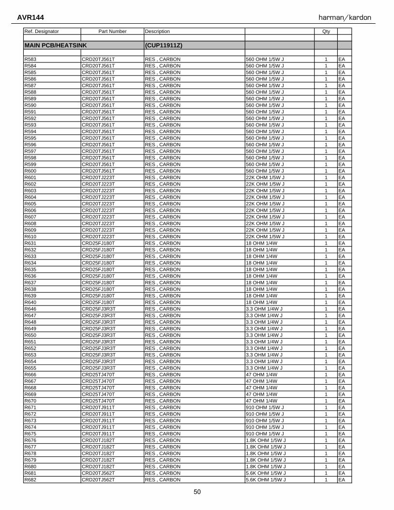
Ref. Designator Part Number Description Qty
MAIN PCB/HEATSINK (CUP11911Z)
R583 CRD20TJ561T RES , CARBON 560 OHM 1/5W J 1 EAR584 CRD20TJ561T RES , CARBON 560 OHM 1/5W J 1 EAR585 CRD20TJ561T RES , CARBON 560 OHM 1/5W J 1 EAR586 CRD20TJ561T RES , CARBON 560 OHM 1/5W J 1 EAR587 CRD20TJ561T RES , CARBON 560 OHM 1/5W J 1 EAR588 CRD20TJ561T RES , CARBON 560 OHM 1/5W J 1 EAR589 CRD20TJ561T RES , CARBON 560 OHM 1/5W J 1 EAR590 CRD20TJ561T RES , CARBON 560 OHM 1/5W J 1 EAR591 CRD20TJ561T RES , CARBON 560 OHM 1/5W J 1 EAR592 CRD20TJ561T RES , CARBON 560 OHM 1/5W J 1 EAR593 CRD20TJ561T RES , CARBON 560 OHM 1/5W J 1 EAR594 CRD20TJ561T RES , CARBON 560 OHM 1/5W J 1 EAR595 CRD20TJ561T RES , CARBON 560 OHM 1/5W J 1 EAR596 CRD20TJ561T RES , CARBON 560 OHM 1/5W J 1 EAR597 CRD20TJ561T RES , CARBON 560 OHM 1/5W J 1 EAR598 CRD20TJ561T RES , CARBON 560 OHM 1/5W J 1 EAR599 CRD20TJ561T RES , CARBON 560 OHM 1/5W J 1 EAR600 CRD20TJ561T RES , CARBON 560 OHM 1/5W J 1 EAR601 CRD20TJ223T RES , CARBON 22K OHM 1/5W J 1 EAR602 CRD20TJ223T RES , CARBON 22K OHM 1/5W J 1 EAR603 CRD20TJ223T RES , CARBON 22K OHM 1/5W J 1 EAR604 CRD20TJ223T RES , CARBON 22K OHM 1/5W J 1 EAR605 CRD20TJ223T RES , CARBON 22K OHM 1/5W J 1 EAR606 CRD20TJ223T RES , CARBON 22K OHM 1/5W J 1 EAR607 CRD20TJ223T RES , CARBON 22K OHM 1/5W J 1 EAR608 CRD20TJ223T RES , CARBON 22K OHM 1/5W J 1 EAR609 CRD20TJ223T RES , CARBON 22K OHM 1/5W J 1 EAR610 CRD20TJ223T RES , CARBON 22K OHM 1/5W J 1 EAR631 CRD25FJ180T RES , CARBON 18 OHM 1/4W 1 EAR632 CRD25FJ180T RES , CARBON 18 OHM 1/4W 1 EAR633 CRD25FJ180T RES , CARBON 18 OHM 1/4W 1 EAR634 CRD25FJ180T RES , CARBON 18 OHM 1/4W 1 EAR635 CRD25FJ180T RES , CARBON 18 OHM 1/4W 1 EAR636 CRD25FJ180T RES , CARBON 18 OHM 1/4W 1 EAR637 CRD25FJ180T RES , CARBON 18 OHM 1/4W 1 EAR638 CRD25FJ180T RES , CARBON 18 OHM 1/4W 1 EAR639 CRD25FJ180T RES , CARBON 18 OHM 1/4W 1 EAR640 CRD25FJ180T RES , CARBON 18 OHM 1/4W 1 EAR646 CRD25FJ3R3T RES , CARBON 3.3 OHM 1/4W J 1 EAR647 CRD25FJ3R3T RES , CARBON 3.3 OHM 1/4W J 1 EAR648 CRD25FJ3R3T RES , CARBON 3.3 OHM 1/4W J 1 EAR649 CRD25FJ3R3T RES , CARBON 3.3 OHM 1/4W J 1 EAR650 CRD25FJ3R3T RES , CARBON 3.3 OHM 1/4W J 1 EAR651 CRD25FJ3R3T RES , CARBON 3.3 OHM 1/4W J 1 EAR652 CRD25FJ3R3T RES , CARBON 3.3 OHM 1/4W J 1 EAR653 CRD25FJ3R3T RES , CARBON 3.3 OHM 1/4W J 1 EAR654 CRD25FJ3R3T RES , CARBON 3.3 OHM 1/4W J 1 EAR655 CRD25FJ3R3T RES , CARBON 3.3 OHM 1/4W J 1 EAR666 CRD25TJ470T RES , CARBON 47 OHM 1/4W 1 EAR667 CRD25TJ470T RES , CARBON 47 OHM 1/4W 1 EAR668 CRD25TJ470T RES , CARBON 47 OHM 1/4W 1 EAR669 CRD25TJ470T RES , CARBON 47 OHM 1/4W 1 EAR670 CRD25TJ470T RES , CARBON 47 OHM 1/4W 1 EAR671 CRD20TJ911T RES , CARBON 910 OHM 1/5W J 1 EAR672 CRD20TJ911T RES , CARBON 910 OHM 1/5W J 1 EAR673 CRD20TJ911T RES , CARBON 910 OHM 1/5W J 1 EAR674 CRD20TJ911T RES , CARBON 910 OHM 1/5W J 1 EAR675 CRD20TJ911T RES , CARBON 910 OHM 1/5W J 1 EAR676 CRD20TJ182T RES , CARBON 1.8K OHM 1/5W J 1 EAR677 CRD20TJ182T RES , CARBON 1.8K OHM 1/5W J 1 EAR678 CRD20TJ182T RES , CARBON 1.8K OHM 1/5W J 1 EAR679 CRD20TJ182T RES , CARBON 1.8K OHM 1/5W J 1 EAR680 CRD20TJ182T RES , CARBON 1.8K OHM 1/5W J 1 EAR681 CRD20TJ562T RES , CARBON 5.6K OHM 1/5W J 1 EAR682 CRD20TJ562T RES , CARBON 5.6K OHM 1/5W J 1 EA
50
AVR144 harman/kardon
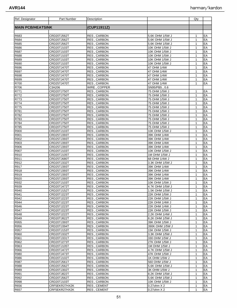
Ref. Designator Part Number Description Qty
MAIN PCB/HEATSINK (CUP11911Z)
R683 CRD20TJ562T RES , CARBON 5.6K OHM 1/5W J 1 EAR684 CRD20TJ562T RES , CARBON 5.6K OHM 1/5W J 1 EAR685 CRD20TJ562T RES , CARBON 5.6K OHM 1/5W J 1 EAR686 CRD20TJ103T RES , CARBON 10K OHM 1/5W J 1 EAR687 CRD20TJ103T RES , CARBON 10K OHM 1/5W J 1 EAR688 CRD20TJ103T RES , CARBON 10K OHM 1/5W J 1 EAR689 CRD20TJ103T RES , CARBON 10K OHM 1/5W J 1 EAR690 CRD20TJ103T RES , CARBON 10K OHM 1/5W J 1 EAR696 CRD25TJ470T RES , CARBON 47 OHM 1/4W 1 EAR697 CRD25TJ470T RES , CARBON 47 OHM 1/4W 1 EAR698 CRD25TJ470T RES , CARBON 47 OHM 1/4W 1 EAR699 CRD25TJ470T RES , CARBON 47 OHM 1/4W 1 EAR700 CRD25TJ470T RES , CARBON 47 OHM 1/4W 1 EAR706 C3A206 WIRE , COPPER SN95/PB5 , 0.6R771 CRD20TJ750T RES , CARBON 75 OHM 1/5W J 1 EAR772 CRD20TJ750T RES , CARBON 75 OHM 1/5W J 1 EAR773 CRD20TJ750T RES , CARBON 75 OHM 1/5W J 1 EAR774 CRD20TJ750T RES , CARBON 75 OHM 1/5W J 1 EAR775 CRD20TJ750T RES , CARBON 75 OHM 1/5W J 1 EAR781 CRD20TJ750T RES , CARBON 75 OHM 1/5W J 1 EAR782 CRD20TJ750T RES , CARBON 75 OHM 1/5W J 1 EAR783 CRD20TJ750T RES , CARBON 75 OHM 1/5W J 1 EAR784 CRD20TJ750T RES , CARBON 75 OHM 1/5W J 1 EAR785 CRD20TJ750T RES , CARBON 75 OHM 1/5W J 1 EAR900 CRD20TJ103T RES , CARBON 10K OHM 1/5W J 1 EAR901 CRD25TJ393T RES , CARBON 39K OHM 1/4W 1 EAR902 CRD25TJ393T RES , CARBON 39K OHM 1/4W 1 EAR903 CRD25TJ393T RES , CARBON 39K OHM 1/4W 1 EAR906 CRD25TJ393T RES , CARBON 39K OHM 1/4W 1 EAR907 CRD20TJ103T RES , CARBON 10K OHM 1/5W J 1 EAR910 CRD20TJ105T RES , CARBON 1M OHM 1/5W J 1 EAR911 CRD25TJ680T RES , CARBON 68 OHM 1/4W J 1 EAR912 CRD20TJ332T RES , CARBON 3.3K OHM 1/5W J 1 EAR917 CRD25TJ393T RES , CARBON 39K OHM 1/4W 1 EAR918 CRD25TJ393T RES , CARBON 39K OHM 1/4W 1 EAR919 CRD25TJ393T RES , CARBON 39K OHM 1/4W 1 EAR920 CRD25TJ393T RES , CARBON 39K OHM 1/4W 1 EAR932 CRD20TJ103T RES , CARBON 10K OHM 1/5W J 1 EAR939 CRD20TJ472T RES , CARBON 4.7K OHM 1/5W J 1 EAR940 CRD20TJ152T RES , CARBON 1.5K OHM 1/5W J 1 EAR941 CRD20TJ223T RES , CARBON 22K OHM 1/5W J 1 EAR942 CRD20TJ223T RES , CARBON 22K OHM 1/5W J 1 EAR944 CRD25TJ223T RES , CARBON 22K OHM 1/4W J 1 EAR946 CRD25TJ223T RES , CARBON 22K OHM 1/4W J 1 EAR947 CRD20TJ223T RES , CARBON 22K OHM 1/5W J 1 EAR948 CRD25TJ222T RES , CARBON 2.2K OHM 1/4W J 1 EAR949 CRD20TJ822T RES , CARBON 8.2K OHM 1/5W J 1 EAR955 CRD20TJ393T RES , CARBON 39K OHM 1/5W J 1 EAR956 CRD20TJ394T RES , CARBON 390K OHM 1/5W J 1 EAR957 CRD20TJ153T RES , CARBON 15K OHM 1/5W J 1 EAR960 CRD20TJ332T RES , CARBON 3.3K OHM 1/5W J 1 EAR961 CRD20TJ331T RES , CARBON 330 OHM 1/5W J 1 EAR962 CRD20TJ273T RES , CARBON 27K OHM 1/5W J 1 EAR963 CRD20TJ105T RES , CARBON 1M OHM 1/5W J 1 EAR966 CRD20TJ472T RES , CARBON 4.7K OHM 1/5W J 1 EAR980 CRD20TJ473T RES , CARBON 47K OHM 1/5W J 1 EAR986 CRD20TJ102T RES , CARBON 1K OHM 1/5W J 1 EAR987 CRD20TJ561T RES , CARBON 560 OHM 1/5W J 1 EAR988 CRD20TJ562T RES , CARBON 5.6K OHM 1/5W J 1 EAR989 CRD20TJ302T RES , CARBON 3K OHM 1/5W J 1 EAR991 CRD20TJ822T RES , CARBON 8.2K OHM 1/5W J 1 EAR992 CRD20TJ562T RES , CARBON 5.6K OHM 1/5W J 1 EAR998 CRD20TJ103T RES , CARBON 10K OHM 1/5W J 1 EAR656 CRF5EKR27HX2K RES , CEMENT 0.27ohm X 2 1 EAR657 CRF5EKR27HX2K RES , CEMENT 0.27ohm X 2 1 EA
51
AVR144 harman/kardon
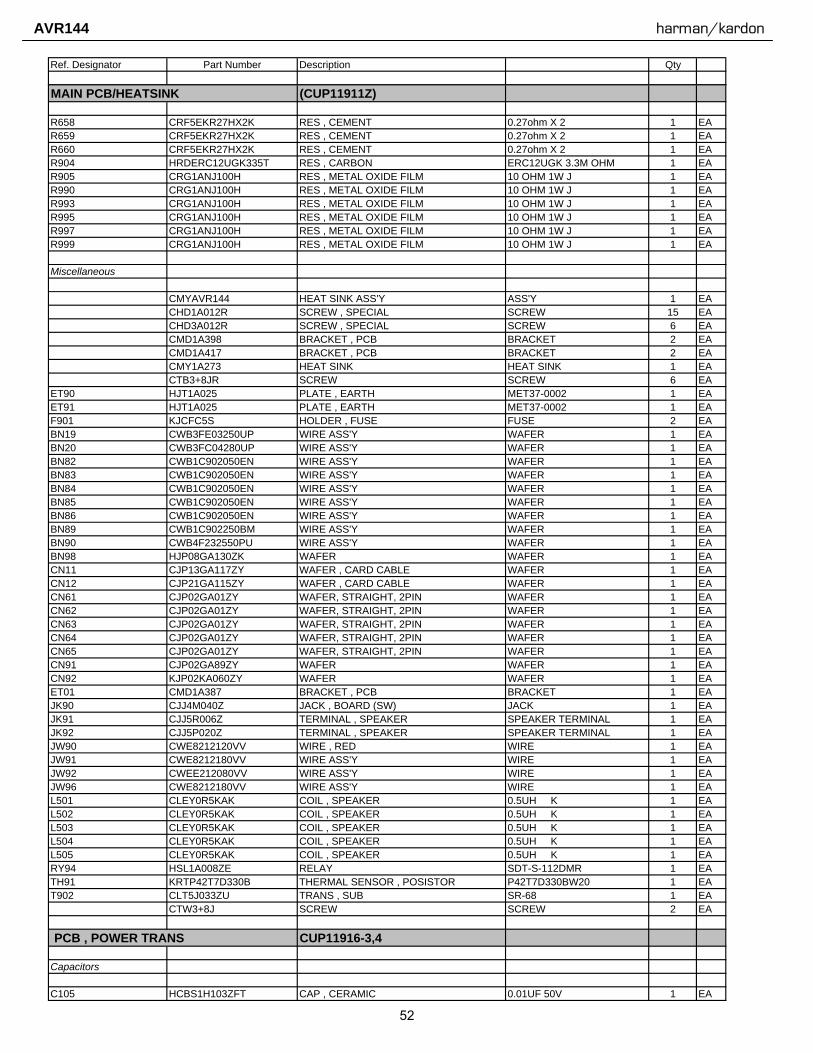
Ref. Designator Part Number Description Qty
MAIN PCB/HEATSINK (CUP11911Z)
R658 CRF5EKR27HX2K RES , CEMENT 0.27ohm X 2 1 EAR659 CRF5EKR27HX2K RES , CEMENT 0.27ohm X 2 1 EAR660 CRF5EKR27HX2K RES , CEMENT 0.27ohm X 2 1 EAR904 HRDERC12UGK335T RES , CARBON ERC12UGK 3.3M OHM 1 EAR905 CRG1ANJ100H RES , METAL OXIDE FILM 10 OHM 1W J 1 EAR990 CRG1ANJ100H RES , METAL OXIDE FILM 10 OHM 1W J 1 EAR993 CRG1ANJ100H RES , METAL OXIDE FILM 10 OHM 1W J 1 EAR995 CRG1ANJ100H RES , METAL OXIDE FILM 10 OHM 1W J 1 EAR997 CRG1ANJ100H RES , METAL OXIDE FILM 10 OHM 1W J 1 EAR999 CRG1ANJ100H RES , METAL OXIDE FILM 10 OHM 1W J 1 EA
Miscellaneous
CMYAVR144 HEAT SINK ASS'Y ASS'Y 1 EACHD1A012R SCREW , SPECIAL SCREW 15 EACHD3A012R SCREW , SPECIAL SCREW 6 EACMD1A398 BRACKET , PCB BRACKET 2 EACMD1A417 BRACKET , PCB BRACKET 2 EACMY1A273 HEAT SINK HEAT SINK 1 EACTB3+8JR SCREW SCREW 6 EA
ET90 HJT1A025 PLATE , EARTH MET37-0002 1 EAET91 HJT1A025 PLATE , EARTH MET37-0002 1 EAF901 KJCFC5S HOLDER , FUSE FUSE 2 EABN19 CWB3FE03250UP WIRE ASS'Y WAFER 1 EABN20 CWB3FC04280UP WIRE ASS'Y WAFER 1 EABN82 CWB1C902050EN WIRE ASS'Y WAFER 1 EABN83 CWB1C902050EN WIRE ASS'Y WAFER 1 EABN84 CWB1C902050EN WIRE ASS'Y WAFER 1 EABN85 CWB1C902050EN WIRE ASS'Y WAFER 1 EABN86 CWB1C902050EN WIRE ASS'Y WAFER 1 EABN89 CWB1C902250BM WIRE ASS'Y WAFER 1 EABN90 CWB4F232550PU WIRE ASS'Y WAFER 1 EABN98 HJP08GA130ZK WAFER WAFER 1 EACN11 CJP13GA117ZY WAFER , CARD CABLE WAFER 1 EACN12 CJP21GA115ZY WAFER , CARD CABLE WAFER 1 EACN61 CJP02GA01ZY WAFER, STRAIGHT, 2PIN WAFER 1 EACN62 CJP02GA01ZY WAFER, STRAIGHT, 2PIN WAFER 1 EACN63 CJP02GA01ZY WAFER, STRAIGHT, 2PIN WAFER 1 EACN64 CJP02GA01ZY WAFER, STRAIGHT, 2PIN WAFER 1 EACN65 CJP02GA01ZY WAFER, STRAIGHT, 2PIN WAFER 1 EACN91 CJP02GA89ZY WAFER WAFER 1 EACN92 KJP02KA060ZY WAFER WAFER 1 EAET01 CMD1A387 BRACKET , PCB BRACKET 1 EAJK90 CJJ4M040Z JACK , BOARD (SW) JACK 1 EAJK91 CJJ5R006Z TERMINAL , SPEAKER SPEAKER TERMINAL 1 EAJK92 CJJ5P020Z TERMINAL , SPEAKER SPEAKER TERMINAL 1 EAJW90 CWE8212120VV WIRE , RED WIRE 1 EAJW91 CWE8212180VV WIRE ASS'Y WIRE 1 EAJW92 CWEE212080VV WIRE ASS'Y WIRE 1 EAJW96 CWE8212180VV WIRE ASS'Y WIRE 1 EAL501 CLEY0R5KAK COIL , SPEAKER 0.5UH K 1 EAL502 CLEY0R5KAK COIL , SPEAKER 0.5UH K 1 EAL503 CLEY0R5KAK COIL , SPEAKER 0.5UH K 1 EAL504 CLEY0R5KAK COIL , SPEAKER 0.5UH K 1 EAL505 CLEY0R5KAK COIL , SPEAKER 0.5UH K 1 EARY94 HSL1A008ZE RELAY SDT-S-112DMR 1 EATH91 KRTP42T7D330B THERMAL SENSOR , POSISTOR P42T7D330BW20 1 EAT902 CLT5J033ZU TRANS , SUB SR-68 1 EA
CTW3+8J SCREW SCREW 2 EA
PCB , POWER TRANS CUP11916-3,4
Capacitors
C105 HCBS1H103ZFT CAP , CERAMIC 0.01UF 50V 1 EA
52
AVR144 harman/kardon

Ref. Designator Part Number Description Qty
PCB , POWER TRANS CUP11916-3,4
C106 CCFT1H104ZF CAP , SEMICONDUCTOR 0.1UF 50V ZF 1 EAC107 HCBS1H103ZFT CAP , CERAMIC 0.01UF 50V 1 EAC108 HCBS1H103ZFT CAP , CERAMIC 0.01UF 50V 1 EAC109 CCFT1H104ZF CAP , SEMICONDUCTOR 0.1UF 50V ZF 1 EAC117 CCEA1HH4R7T CAP , ELECT 4.7UF 50V 1 EAC118 HCBS1H103ZFT CAP , CERAMIC 0.01UF 50V 1 EAC119 CCEA1JH470TS CAP , ELECT 63V/47UF/105'C 1 EAC120 CCEA1JH470TS CAP , ELECT 63V/47UF/105'C 1 EAC121 HCBS1H103ZFT CAP , CERAMIC 0.01UF 50V 1 EAC122 CCEA1JH101E CAP , ELECT 100UF 63V 1 EAC125 CCFT1H473ZF CAP, CERAMIC 0.047UF 50V ZF 1 EAC126 CCFT1H473ZF CAP, CERAMIC 0.047UF 50V ZF 1 EAC128 CCEA1EH102E CAP , ELECT 1000UF 25V 1 EAC129 CCEA1EH222E CAP , ELECT 2200UF 25V 1 EAC131 CCEA1HH4R7T CAP , ELECT 4.7UF 50V 1 EAC919 CCKT1H102KB CAP , CERAMIC 1000PF 50V 1 EAC920 CCEA1HH470T CAP , ELECT 47UF 50V 1 EAC921 HCQI1H104JZT CAP , MYLAR 0.1UF 50V J 1 EAC922 HCQI1H104JZT CAP , MYLAR 0.1UF 50V J 1 EAC923 HCQI1H104JZT CAP , MYLAR 0.1UF 50V J 1 EAC924 HCQI1H104JZT CAP , MYLAR 0.1UF 50V J 1 EAC925 HCQI1H103JZT CAP , MYLAR 0.01UF 50V J 1 EAC926 HCQI1H103JZT CAP , MYLAR 0.01UF 50V J 1 EAC927 HCQI1H103JZT CAP , MYLAR 0.01UF 50V J 1 EAC928 HCQI1H103JZT CAP , MYLAR 0.01UF 50V J 1 EAC931 HCQI1H473JZT CAP , MYLAR 0.047UF 50V J 1 EAC932 HCQI1H473JZT CAP , MYLAR 0.047UF 50V J 1 EAC933 HCQI1H473JZT CAP , MYLAR 0.047UF 50V J 1 EAC934 HCQI1H473JZT CAP , MYLAR 0.047UF 50V J 1 EAC104 HCBS1H103ZFT CAP , CERAMIC 0.01UF 50V 1 EA
Semiconductors
D101 HVDMTZJ15BT DIODE , ZENER 15V 1/2W 1 EAD102 HVDMTZJ27BT DIODE , ZENER 27V 1/2W 1 EAD104 CVD1N4003ST RECT , DIODE 1N4003 1 EAD105 CVD1N4003ST RECT , DIODE 1N4003 1 EAD108 CVD1N4003ST RECT , DIODE 1N4003 1 EAD109 HVDMTZJ12BT DIODE , ZENER 12V 1/2W 1 EAD111 HVDMTZJ12BT DIODE , ZENER 12V 1/2W 1 EAD114 CVD1N4003ST RECT , DIODE 1N4003 1 EAD115 CVD1N4003ST RECT , DIODE 1N4003 1 EAD116 CVD1N4003ST RECT , DIODE 1N4003 1 EAD117 CVD1N4003ST RECT , DIODE 1N4003 1 EAD118 CVD1N4003ST RECT , DIODE 1N4003 1 EAD119 CVD1N4003ST RECT , DIODE 1N4003 1 EAD120 CVD1N4003ST RECT , DIODE 1N4003 1 EAD121 CVD1N4003ST RECT , DIODE 1N4003 1 EAD124 CVD1N4003ST RECT , DIODE 1N4003 1 EAD125 CVD1N4003ST RECT , DIODE 1N4003 1 EAD991 HVDKBU804F DIODE , BRIDGE KBU804F 1 EAD992 HVDKBU804F DIODE , BRIDGE KBU804F 1 EAQ104 HVTKSC2316YT TRANSISTOR NPN KSC2316Y 1 EAQ911 HVTKTA1267YT TRANSISTOR PNP KTA1267Y 1 EAQ912 HVTKTC3198YT TRANSISTOR NPN KTC3198Y 1 EAQ913 HVTKTC3198YT TRANSISTOR NPN KTC3198Y 1 EA
Resistors
R101 CRD25FJ3R3T RES , CARBON 3.3 OHM 1/4W J 1 EAR104 KRQ1AJR47H RES , FUSE 0.47 OHM 1W J 1 EAR105 KRQ1AJR47H RES , FUSE 0.47 OHM 1W J 1 EAR106 CRQ1AJR33H RES , FUSE 0.33 OHM 1W J 1 EAR107 CRQ1AJR33H RES , FUSE 0.33 OHM 1W J 1 EAR116 CRQ1AJR33H RES , FUSE 0.33 OHM 1W J 1 EA
53
AVR144 harman/kardon
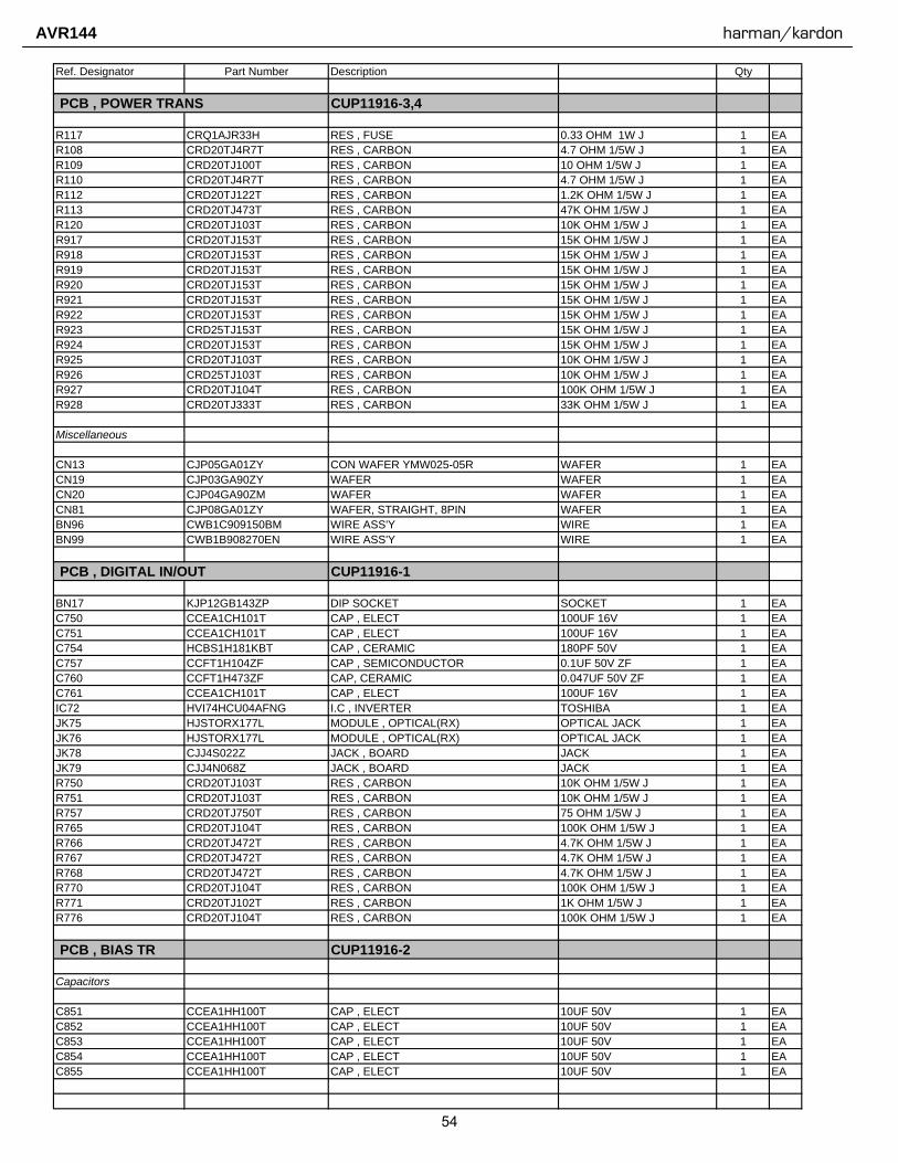
Ref. Designator Part Number Description Qty
PCB , POWER TRANS CUP11916-3,4
R117 CRQ1AJR33H RES , FUSE 0.33 OHM 1W J 1 EAR108 CRD20TJ4R7T RES , CARBON 4.7 OHM 1/5W J 1 EAR109 CRD20TJ100T RES , CARBON 10 OHM 1/5W J 1 EAR110 CRD20TJ4R7T RES , CARBON 4.7 OHM 1/5W J 1 EAR112 CRD20TJ122T RES , CARBON 1.2K OHM 1/5W J 1 EAR113 CRD20TJ473T RES , CARBON 47K OHM 1/5W J 1 EAR120 CRD20TJ103T RES , CARBON 10K OHM 1/5W J 1 EAR917 CRD20TJ153T RES , CARBON 15K OHM 1/5W J 1 EAR918 CRD20TJ153T RES , CARBON 15K OHM 1/5W J 1 EAR919 CRD20TJ153T RES , CARBON 15K OHM 1/5W J 1 EAR920 CRD20TJ153T RES , CARBON 15K OHM 1/5W J 1 EAR921 CRD20TJ153T RES , CARBON 15K OHM 1/5W J 1 EAR922 CRD20TJ153T RES , CARBON 15K OHM 1/5W J 1 EAR923 CRD25TJ153T RES , CARBON 15K OHM 1/5W J 1 EAR924 CRD20TJ153T RES , CARBON 15K OHM 1/5W J 1 EAR925 CRD20TJ103T RES , CARBON 10K OHM 1/5W J 1 EAR926 CRD25TJ103T RES , CARBON 10K OHM 1/5W J 1 EAR927 CRD20TJ104T RES , CARBON 100K OHM 1/5W J 1 EAR928 CRD20TJ333T RES , CARBON 33K OHM 1/5W J 1 EA
Miscellaneous
CN13 CJP05GA01ZY CON WAFER YMW025-05R WAFER 1 EACN19 CJP03GA90ZY WAFER WAFER 1 EACN20 CJP04GA90ZM WAFER WAFER 1 EACN81 CJP08GA01ZY WAFER, STRAIGHT, 8PIN WAFER 1 EABN96 CWB1C909150BM WIRE ASS'Y WIRE 1 EABN99 CWB1B908270EN WIRE ASS'Y WIRE 1 EA
PCB , DIGITAL IN/OUT CUP11916-1
BN17 KJP12GB143ZP DIP SOCKET SOCKET 1 EAC750 CCEA1CH101T CAP , ELECT 100UF 16V 1 EAC751 CCEA1CH101T CAP , ELECT 100UF 16V 1 EAC754 HCBS1H181KBT CAP , CERAMIC 180PF 50V 1 EAC757 CCFT1H104ZF CAP , SEMICONDUCTOR 0.1UF 50V ZF 1 EAC760 CCFT1H473ZF CAP, CERAMIC 0.047UF 50V ZF 1 EAC761 CCEA1CH101T CAP , ELECT 100UF 16V 1 EAIC72 HVI74HCU04AFNG I.C , INVERTER TOSHIBA 1 EAJK75 HJSTORX177L MODULE , OPTICAL(RX) OPTICAL JACK 1 EAJK76 HJSTORX177L MODULE , OPTICAL(RX) OPTICAL JACK 1 EAJK78 CJJ4S022Z JACK , BOARD JACK 1 EAJK79 CJJ4N068Z JACK , BOARD JACK 1 EAR750 CRD20TJ103T RES , CARBON 10K OHM 1/5W J 1 EAR751 CRD20TJ103T RES , CARBON 10K OHM 1/5W J 1 EAR757 CRD20TJ750T RES , CARBON 75 OHM 1/5W J 1 EAR765 CRD20TJ104T RES , CARBON 100K OHM 1/5W J 1 EAR766 CRD20TJ472T RES , CARBON 4.7K OHM 1/5W J 1 EAR767 CRD20TJ472T RES , CARBON 4.7K OHM 1/5W J 1 EAR768 CRD20TJ472T RES , CARBON 4.7K OHM 1/5W J 1 EAR770 CRD20TJ104T RES , CARBON 100K OHM 1/5W J 1 EAR771 CRD20TJ102T RES , CARBON 1K OHM 1/5W J 1 EAR776 CRD20TJ104T RES , CARBON 100K OHM 1/5W J 1 EA
PCB , BIAS TR CUP11916-2
Capacitors
C851 CCEA1HH100T CAP , ELECT 10UF 50V 1 EAC852 CCEA1HH100T CAP , ELECT 10UF 50V 1 EAC853 CCEA1HH100T CAP , ELECT 10UF 50V 1 EAC854 CCEA1HH100T CAP , ELECT 10UF 50V 1 EAC855 CCEA1HH100T CAP , ELECT 10UF 50V 1 EA
54
AVR144 harman/kardon
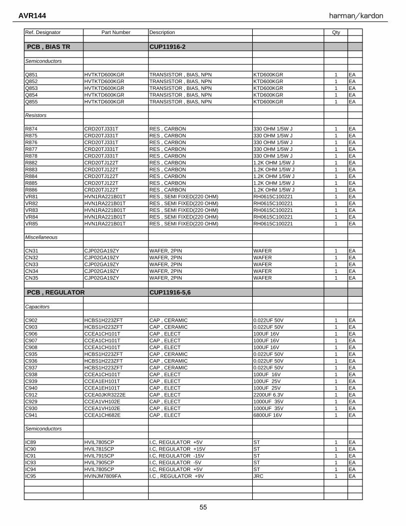
Ref. Designator Part Number Description Qty
PCB , BIAS TR CUP11916-2
Semiconductors
Q851 HVTKTD600KGR TRANSISTOR , BIAS, NPN KTD600KGR 1 EAQ852 HVTKTD600KGR TRANSISTOR , BIAS, NPN KTD600KGR 1 EAQ853 HVTKTD600KGR TRANSISTOR , BIAS, NPN KTD600KGR 1 EAQ854 HVTKTD600KGR TRANSISTOR , BIAS, NPN KTD600KGR 1 EAQ855 HVTKTD600KGR TRANSISTOR , BIAS, NPN KTD600KGR 1 EA
Resistors
R874 CRD20TJ331T RES , CARBON 330 OHM 1/5W J 1 EAR875 CRD20TJ331T RES , CARBON 330 OHM 1/5W J 1 EAR876 CRD20TJ331T RES , CARBON 330 OHM 1/5W J 1 EAR877 CRD20TJ331T RES , CARBON 330 OHM 1/5W J 1 EAR878 CRD20TJ331T RES , CARBON 330 OHM 1/5W J 1 EAR882 CRD20TJ122T RES , CARBON 1.2K OHM 1/5W J 1 EAR883 CRD20TJ122T RES , CARBON 1.2K OHM 1/5W J 1 EAR884 CRD20TJ122T RES , CARBON 1.2K OHM 1/5W J 1 EAR885 CRD20TJ122T RES , CARBON 1.2K OHM 1/5W J 1 EAR886 CRD20TJ122T RES , CARBON 1.2K OHM 1/5W J 1 EAVR81 HVN1RA221B01T RES , SEMI FIXED(220 OHM) RH0615C100221 1 EAVR82 HVN1RA221B01T RES , SEMI FIXED(220 OHM) RH0615C100221 1 EAVR83 HVN1RA221B01T RES , SEMI FIXED(220 OHM) RH0615C100221 1 EAVR84 HVN1RA221B01T RES , SEMI FIXED(220 OHM) RH0615C100221 1 EAVR85 HVN1RA221B01T RES , SEMI FIXED(220 OHM) RH0615C100221 1 EA
Miscellaneous
CN31 CJP02GA19ZY WAFER, 2PIN WAFER 1 EACN32 CJP02GA19ZY WAFER, 2PIN WAFER 1 EACN33 CJP02GA19ZY WAFER, 2PIN WAFER 1 EACN34 CJP02GA19ZY WAFER, 2PIN WAFER 1 EACN35 CJP02GA19ZY WAFER, 2PIN WAFER 1 EA
PCB , REGULATOR CUP11916-5,6
Capacitors
C902 HCBS1H223ZFT CAP , CERAMIC 0.022UF 50V 1 EAC903 HCBS1H223ZFT CAP , CERAMIC 0.022UF 50V 1 EAC906 CCEA1CH101T CAP , ELECT 100UF 16V 1 EAC907 CCEA1CH101T CAP , ELECT 100UF 16V 1 EAC908 CCEA1CH101T CAP , ELECT 100UF 16V 1 EAC935 HCBS1H223ZFT CAP , CERAMIC 0.022UF 50V 1 EAC936 HCBS1H223ZFT CAP , CERAMIC 0.022UF 50V 1 EAC937 HCBS1H223ZFT CAP , CERAMIC 0.022UF 50V 1 EAC938 CCEA1CH101T CAP , ELECT 100UF 16V 1 EAC939 CCEA1EH101T CAP , ELECT 100UF 25V 1 EAC940 CCEA1EH101T CAP , ELECT 100UF 25V 1 EAC912 CCEA0JKR3222E CAP , ELECT 2200UF 6.3V 1 EAC929 CCEA1VH102E CAP , ELECT 1000UF 35V 1 EAC930 CCEA1VH102E CAP , ELECT 1000UF 35V 1 EAC941 CCEA1CH682E CAP , ELECT 6800UF 16V 1 EA
Semiconductors
IC89 HVIL7805CP I.C, REGULATOR +5V ST 1 EAIC90 HVIL7815CP I.C, REGULATOR +15V ST 1 EAIC91 HVIL7915CP I.C, REGULATOR -15V ST 1 EAIC93 HVIL7905CP I.C, REGULATOR -5V ST 1 EAIC94 HVIL7805CP I.C, REGULATOR +5V ST 1 EAIC95 HVINJM7809FA I.C , REGULATOR +9V JRC 1 EA
55
AVR144 harman/kardon

Ref. Designator Part Number Description Qty
PCB , REGULATOR CUP11916-5,6
Resistors
R912 CRD20TJ153T RES , CARBON 15K OHM 1/5W J 1 EAR913 CRD20TJ153T RES , CARBON 15K OHM 1/5W J 1 EA
Miscellaneous
BN20 CWB1C905200BM WIRE ASS'Y WIRE 1 EABN43 CWB1C904200BM WIRE ASS'Y WIRE 1 EABN95 CWB1C903080EN WIRE ASS'Y WIRE 1 EACN89 CJP02GA01ZY WAFER, STRAIGHT, 2PIN WAFER 1 EACN95 CJP03GA19ZY WAFER, STRAIGHT, 3PIN WAFER 1 EACN96 CJP09GA01ZY CON WAFER YMW025-09R WAFER 1 EACN98 HJP08GB131ZK WAFER WAFER 1 EACN99 CJP08GA19ZY WAFER, STRAIGHT, 8PIN WAFER 1 EA
PCB , INPUT CUP11912-1
Capacitors
C201 CCUS1H221JA CAP , CHIP 220PF 1 EAC202 CCUS1H221JA CAP , CHIP 220PF 1 EAC203 CCUS1H221JA CAP , CHIP 220PF 1 EAC204 CCUS1H221JA CAP , CHIP 220PF 1 EAC205 CCUS1H221JA CAP , CHIP 220PF 1 EAC206 CCUS1H221JA CAP , CHIP 220PF 1 EAC209 CCUS1H221JA CAP , CHIP 220PF 1 EAC210 CCUS1H221JA CAP , CHIP 220PF 1 EAC211 CCUS1H221JA CAP , CHIP 220PF 1 EAC212 CCUS1H221JA CAP , CHIP 220PF 1 EAC213 CCUS1H221JA CAP , CHIP 220PF 1 EAC214 CCUS1H221JA CAP , CHIP 220PF 1 EAC215 CCUS1H221JA CAP , CHIP 220PF 1 EAC216 CCUS1H221JA CAP , CHIP 220PF 1 EAC219 CCUS1H221JA CAP , CHIP 220PF 1 EAC220 CCUS1H221JA CAP , CHIP 220PF 1 EAC221 CCUS1H221JA CAP , CHIP 220PF 1 EAC222 CCUS1H221JA CAP , CHIP 220PF 1 EAC223 CCUS1H221JA CAP , CHIP 220PF 1 EAC224 CCUS1H221JA CAP , CHIP 220PF 1 EAC260 CCUS1H104KC CAP , CHIP 0.1UF 1 EAC269 CCUS1A105KC CAP , CHIP 1UF 1 EAC274 CCUS1A105KC CAP , CHIP 1UF 1 EAC277 CCUS1H104KC CAP , CHIP 0.1UF 1 EAC279 CCUS1H104KC CAP , CHIP 0.1UF 1 EAC280 CCUS1H104KC CAP , CHIP 0.1UF 1 EAC289 CCUS1H104KC CAP , CHIP 0.1UF 1 EAC290 CCUS1H104KC CAP , CHIP 0.1UF 1 EAC291 CCUS1H104KC CAP , CHIP 0.1UF 1 EAC293 CCUS1H104KC CAP , CHIP 0.1UF 1 EAC299 CCUS1H104KC CAP , CHIP 0.1UF 1 EAC301 CCUS1H471JA CAP , CHIP 470PF 1 EAC302 CCUS1H471JA CAP , CHIP 470PF 1 EAC303 CCUS1H471JA CAP , CHIP 470PF 1 EAC304 CCUS1H471JA CAP , CHIP 470PF 1 EAC305 CCUS1H471JA CAP , CHIP 470PF 1 EAC306 CCUS1H471JA CAP , CHIP 470PF 1 EAC309 CCUS1H332KC CAP , CHIP 3300PF 1 EAC310 CCUS1H332KC CAP , CHIP 3300PF 1 EAC311 CCUS1H332KC CAP , CHIP 3300PF 1 EAC312 CCUS1H332KC CAP , CHIP 3300PF 1 EAC313 CCUS1H332KC CAP , CHIP 3300PF 1 EAC314 CCUS1H332KC CAP , CHIP 3300PF 1 EAC317 CCUS1H223KC CAP , CHIP 0.022UF 1 EAC318 CCUS1H223KC CAP , CHIP 0.022UF 1 EA
56
AVR144 harman/kardon
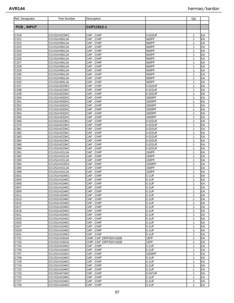
Ref. Designator Part Number Description Qty
PCB , INPUT CUP11912-1
C319 CCUS1H223KC CAP , CHIP 0.022UF 1 EAC321 CCUS1H561JA CAP , CHIP 560PF 1 EAC322 CCUS1H561JA CAP , CHIP 560PF 1 EAC323 CCUS1H561JA CAP , CHIP 560PF 1 EAC324 CCUS1H561JA CAP , CHIP 560PF 1 EAC325 CCUS1H561JA CAP , CHIP 560PF 1 EAC326 CCUS1H561JA CAP , CHIP 560PF 1 EAC327 CCUS1H561JA CAP , CHIP 560PF 1 EAC328 CCUS1H561JA CAP , CHIP 560PF 1 EAC329 CCUS1H561JA CAP , CHIP 560PF 1 EAC330 CCUS1H561JA CAP , CHIP 560PF 1 EAC331 CCUS1H561JA CAP , CHIP 560PF 1 EAC332 CCUS1H561JA CAP , CHIP 560PF 1 EAC337 CCUS1H223KC CAP , CHIP 0.022UF 1 EAC338 CCUS1H223KC CAP , CHIP 0.022UF 1 EAC339 CCUS1H223KC CAP , CHIP 0.022UF 1 EAC350 CCUS1H332KC CAP , CHIP 3300PF 1 EAC351 CCUS1H332KC CAP , CHIP 3300PF 1 EAC352 CCUS1H332KC CAP , CHIP 3300PF 1 EAC353 CCUS1H332KC CAP , CHIP 3300PF 1 EAC354 CCUS1H332KC CAP , CHIP 3300PF 1 EAC355 CCUS1H332KC CAP , CHIP 3300PF 1 EAC369 CCUS1H223KC CAP , CHIP 0.022UF 1 EAC370 CCUS1H223KC CAP , CHIP 0.022UF 1 EAC381 CCUS1H223KC CAP , CHIP 0.022UF 1 EAC382 CCUS1H223KC CAP , CHIP 0.022UF 1 EAC383 CCUS1H223KC CAP , CHIP 0.022UF 1 EAC384 CCUS1H223KC CAP , CHIP 0.022UF 1 EAC385 CCUS1H223KC CAP , CHIP 0.022UF 1 EAC386 CCUS1H223KC CAP , CHIP 0.022UF 1 EAC391 CCUS1H151JA CAP , CHIP 150PF 1 EAC392 CCUS1H151JA CAP , CHIP 150PF 1 EAC393 CCUS1H151JA CAP , CHIP 150PF 1 EAC394 CCUS1H102KC CAP , CHIP 1000PF 1 EAC395 CCUS1H151JA CAP , CHIP 150PF 1 EAC396 CCUS1H151JA CAP , CHIP 150PF 1 EAC601 CCUS1H104KC CAP , CHIP 0.1UF 1 EAC603 CCUS1H104KC CAP , CHIP 0.1UF 1 EAC605 CCUS1H104KC CAP , CHIP 0.1UF 1 EAC607 CCUS1H104KC CAP , CHIP 0.1UF 1 EAC609 CCUS1H104KC CAP , CHIP 0.1UF 1 EAC611 CCUS1H104KC CAP , CHIP 0.1UF 1 EAC613 CCUS1H104KC CAP , CHIP 0.1UF 1 EAC615 CCUS1H104KC CAP , CHIP 0.1UF 1 EAC617 CCUS1H104KC CAP , CHIP 0.1UF 1 EAC619 CCUS1H104KC CAP , CHIP 0.1UF 1 EAC621 CCUS1H104KC CAP , CHIP 0.1UF 1 EAC623 CCUS1H104KC CAP , CHIP 0.1UF 1 EAC625 CCUS1H104KC CAP , CHIP 0.1UF 1 EAC627 CCUS1H104KC CAP , CHIP 0.1UF 1 EAC629 CCUS1H104KC CAP , CHIP 0.1UF 1 EAC631 CCUS1H104KC CAP , CHIP 0.1UF 1 EAC701 CCUS1H150JA CHIP, CAP 15PF/50V/1608 15PF 1 EAC702 CCUS1H150JA CHIP, CAP 15PF/50V/1608 15PF 1 EAC704 CCUS1H104KC CAP , CHIP 0.1UF 1 EAC705 CCUS1H104KC CAP , CHIP 0.1UF 1 EAC707 CCUS1H102KC CAP , CHIP 1000PF 1 EAC708 CCUS1H104KC CAP , CHIP 0.1UF 1 EAC718 CCUS1H104KC CAP , CHIP 0.1UF 1 EAC719 CCUS1H104KC CAP , CHIP 0.1UF 1 EAC722 CCUS1H104KC CAP , CHIP 0.1UF 1 EAC723 CCUS1H473KC CAP , CHIP 0.047UF 1 EAC725 CCUS1H104KC CAP , CHIP 0.1UF 1 EAC727 CCUS1H104KC CAP , CHIP 0.1UF 1 EAC729 CCUS1H104KC CAP , CHIP 0.1UF 1 EA
57
AVR144 harman/kardon
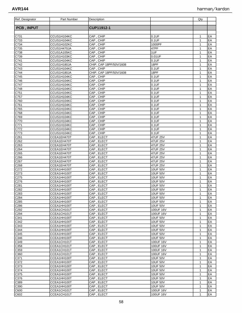
Ref. Designator Part Number Description Qty
PCB , INPUT CUP11912-1
C731 CCUS1H104KC CAP , CHIP 0.1UF 1 EAC733 CCUS1H104KC CAP , CHIP 0.1UF 1 EAC734 CCUS1H102KC CAP , CHIP 1000PF 1 EAC735 CCUS1H470JA CAP , CHIP 47PF 1 EAC738 CCUS1A105KC CAP , CHIP 1UF 1 EAC739 CCUS1H103KC CAP , CHIP 0.01UF 1 EAC741 CCUS1H104KC CAP , CHIP 0.1UF 1 EAC742 CCUS1H180JA CHIP, CAP 18PF/50V/1608 18PF 1 EAC743 CCUS1H104KC CAP , CHIP 0.1UF 1 EAC744 CCUS1H180JA CHIP, CAP 18PF/50V/1608 18PF 1 EAC745 CCUS1H104KC CAP , CHIP 0.1UF 1 EAC746 CCUS1H104KC CAP , CHIP 0.1UF 1 EAC747 CCUS1H104KC CAP , CHIP 0.1UF 1 EAC748 CCUS1H104KC CAP , CHIP 0.1UF 1 EAC751 CCUS1H104KC CAP , CHIP 0.1UF 1 EAC757 CCUS1H104KC CAP , CHIP 0.1UF 1 EAC760 CCUS1H104KC CAP , CHIP 0.1UF 1 EAC761 CCUS1H104KC CAP , CHIP 0.1UF 1 EAC765 CCUS1H104KC CAP , CHIP 0.1UF 1 EAC768 CCUS1H104KC CAP , CHIP 0.1UF 1 EAC769 CCUS1H104KC CAP , CHIP 0.1UF 1 EAC770 CCUS1H104KC CAP , CHIP 0.1UF 1 EAC771 CCUS1H104KC CAP , CHIP 0.1UF 1 EAC772 CCUS1H104KC CAP , CHIP 0.1UF 1 EAC773 CCUS1H104KC CAP , CHIP 0.1UF 1 EAC261 CCEA1EH470T CAP , ELECT 47UF 25V 1 EAC262 CCEA1EH470T CAP , ELECT 47UF 25V 1 EAC263 CCEA1EH470T CAP , ELECT 47UF 25V 1 EAC264 CCEA1EH470T CAP , ELECT 47UF 25V 1 EAC265 CCEA1EH470T CAP , ELECT 47UF 25V 1 EAC266 CCEA1EH470T CAP , ELECT 47UF 25V 1 EAC267 CCEA1EH470T CAP , ELECT 47UF 25V 1 EAC268 CCEA1EH470T CAP , ELECT 47UF 25V 1 EAC272 CCEA1HH100T CAP , ELECT 10UF 50V 1 EAC273 CCEA1HH100T CAP , ELECT 10UF 50V 1 EAC275 CCEA1HH100T CAP , ELECT 10UF 50V 1 EAC276 CCEA1HH100T CAP , ELECT 10UF 50V 1 EAC281 CCEA1HH100T CAP , ELECT 10UF 50V 1 EAC282 CCEA1HH100T CAP , ELECT 10UF 50V 1 EAC283 CCEA1HH100T CAP , ELECT 10UF 50V 1 EAC284 CCEA1HH100T CAP , ELECT 10UF 50V 1 EAC285 CCEA1HH100T CAP , ELECT 10UF 50V 1 EAC286 CCEA1HH100T CAP , ELECT 10UF 50V 1 EAC292 CCEA1CH101T CAP , ELECT 100UF 16V 1 EAC294 CCEA1CH101T CAP , ELECT 100UF 16V 1 EAC341 CCEA1HH100T CAP , ELECT 10UF 50V 1 EAC342 CCEA1HH100T CAP , ELECT 10UF 50V 1 EAC343 CCEA1HH100T CAP , ELECT 10UF 50V 1 EAC344 CCEA1HH100T CAP , ELECT 10UF 50V 1 EAC345 CCEA1HH100T CAP , ELECT 10UF 50V 1 EAC346 CCEA1HH100T CAP , ELECT 10UF 50V 1 EAC349 CCEA1CH101T CAP , ELECT 100UF 16V 1 EAC358 CCEA1CH101T CAP , ELECT 100UF 16V 1 EAC359 CCEA1CH101T CAP , ELECT 100UF 16V 1 EAC360 CCEA1CH101T CAP , ELECT 100UF 16V 1 EAC371 CCEA1HH100T CAP , ELECT 10UF 50V 1 EAC372 CCEA1HH100T CAP , ELECT 10UF 50V 1 EAC373 CCEA1HH100T CAP , ELECT 10UF 50V 1 EAC374 CCEA1HH100T CAP , ELECT 10UF 50V 1 EAC375 CCEA1HH100T CAP , ELECT 10UF 50V 1 EAC376 CCEA1HH100T CAP , ELECT 10UF 50V 1 EAC389 CCEA1HH100T CAP , ELECT 10UF 50V 1 EAC390 CCEA1HH100T CAP , ELECT 10UF 50V 1 EAC600 CCEA1CH101T CAP , ELECT 100UF 16V 1 EAC602 CCEA1CH101T CAP , ELECT 100UF 16V 1 EA
58
AVR144 harman/kardon
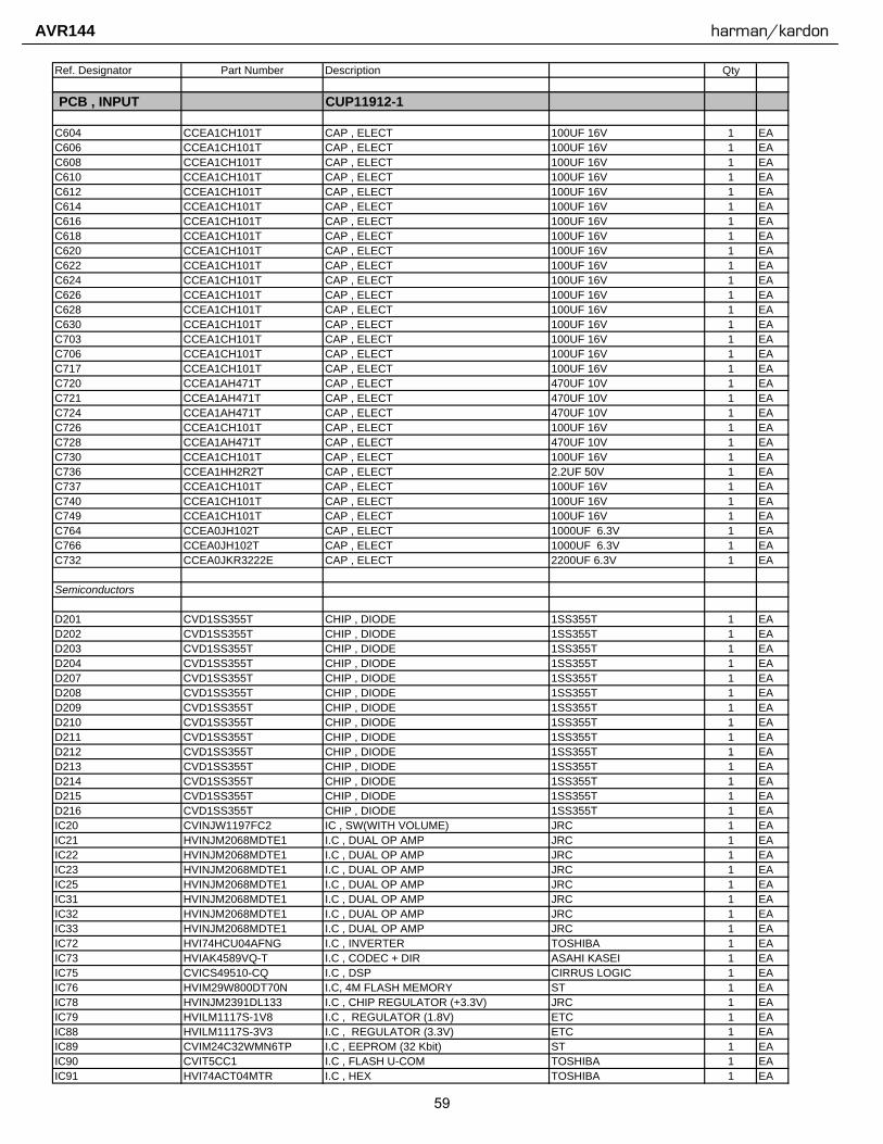
Ref. Designator Part Number Description Qty
PCB , INPUT CUP11912-1
C604 CCEA1CH101T CAP , ELECT 100UF 16V 1 EAC606 CCEA1CH101T CAP , ELECT 100UF 16V 1 EAC608 CCEA1CH101T CAP , ELECT 100UF 16V 1 EAC610 CCEA1CH101T CAP , ELECT 100UF 16V 1 EAC612 CCEA1CH101T CAP , ELECT 100UF 16V 1 EAC614 CCEA1CH101T CAP , ELECT 100UF 16V 1 EAC616 CCEA1CH101T CAP , ELECT 100UF 16V 1 EAC618 CCEA1CH101T CAP , ELECT 100UF 16V 1 EAC620 CCEA1CH101T CAP , ELECT 100UF 16V 1 EAC622 CCEA1CH101T CAP , ELECT 100UF 16V 1 EAC624 CCEA1CH101T CAP , ELECT 100UF 16V 1 EAC626 CCEA1CH101T CAP , ELECT 100UF 16V 1 EAC628 CCEA1CH101T CAP , ELECT 100UF 16V 1 EAC630 CCEA1CH101T CAP , ELECT 100UF 16V 1 EAC703 CCEA1CH101T CAP , ELECT 100UF 16V 1 EAC706 CCEA1CH101T CAP , ELECT 100UF 16V 1 EAC717 CCEA1CH101T CAP , ELECT 100UF 16V 1 EAC720 CCEA1AH471T CAP , ELECT 470UF 10V 1 EAC721 CCEA1AH471T CAP , ELECT 470UF 10V 1 EAC724 CCEA1AH471T CAP , ELECT 470UF 10V 1 EAC726 CCEA1CH101T CAP , ELECT 100UF 16V 1 EAC728 CCEA1AH471T CAP , ELECT 470UF 10V 1 EAC730 CCEA1CH101T CAP , ELECT 100UF 16V 1 EAC736 CCEA1HH2R2T CAP , ELECT 2.2UF 50V 1 EAC737 CCEA1CH101T CAP , ELECT 100UF 16V 1 EAC740 CCEA1CH101T CAP , ELECT 100UF 16V 1 EAC749 CCEA1CH101T CAP , ELECT 100UF 16V 1 EAC764 CCEA0JH102T CAP , ELECT 1000UF 6.3V 1 EAC766 CCEA0JH102T CAP , ELECT 1000UF 6.3V 1 EAC732 CCEA0JKR3222E CAP , ELECT 2200UF 6.3V 1 EA
Semiconductors
D201 CVD1SS355T CHIP , DIODE 1SS355T 1 EAD202 CVD1SS355T CHIP , DIODE 1SS355T 1 EAD203 CVD1SS355T CHIP , DIODE 1SS355T 1 EAD204 CVD1SS355T CHIP , DIODE 1SS355T 1 EAD207 CVD1SS355T CHIP , DIODE 1SS355T 1 EAD208 CVD1SS355T CHIP , DIODE 1SS355T 1 EAD209 CVD1SS355T CHIP , DIODE 1SS355T 1 EAD210 CVD1SS355T CHIP , DIODE 1SS355T 1 EAD211 CVD1SS355T CHIP , DIODE 1SS355T 1 EAD212 CVD1SS355T CHIP , DIODE 1SS355T 1 EAD213 CVD1SS355T CHIP , DIODE 1SS355T 1 EAD214 CVD1SS355T CHIP , DIODE 1SS355T 1 EAD215 CVD1SS355T CHIP , DIODE 1SS355T 1 EAD216 CVD1SS355T CHIP , DIODE 1SS355T 1 EAIC20 CVINJW1197FC2 IC , SW(WITH VOLUME) JRC 1 EAIC21 HVINJM2068MDTE1 I.C , DUAL OP AMP JRC 1 EAIC22 HVINJM2068MDTE1 I.C , DUAL OP AMP JRC 1 EAIC23 HVINJM2068MDTE1 I.C , DUAL OP AMP JRC 1 EAIC25 HVINJM2068MDTE1 I.C , DUAL OP AMP JRC 1 EAIC31 HVINJM2068MDTE1 I.C , DUAL OP AMP JRC 1 EAIC32 HVINJM2068MDTE1 I.C , DUAL OP AMP JRC 1 EAIC33 HVINJM2068MDTE1 I.C , DUAL OP AMP JRC 1 EAIC72 HVI74HCU04AFNG I.C , INVERTER TOSHIBA 1 EAIC73 HVIAK4589VQ-T I.C , CODEC + DIR ASAHI KASEI 1 EAIC75 CVICS49510-CQ I.C , DSP CIRRUS LOGIC 1 EAIC76 HVIM29W800DT70N I.C, 4M FLASH MEMORY ST 1 EAIC78 HVINJM2391DL133 I.C , CHIP REGULATOR (+3.3V) JRC 1 EAIC79 HVILM1117S-1V8 I.C , REGULATOR (1.8V) ETC 1 EAIC88 HVILM1117S-3V3 I.C , REGULATOR (3.3V) ETC 1 EAIC89 CVIM24C32WMN6TP I.C , EEPROM (32 Kbit) ST 1 EAIC90 CVIT5CC1 I.C , FLASH U-COM TOSHIBA 1 EAIC91 HVI74ACT04MTR I.C , HEX TOSHIBA 1 EA
59
AVR144 harman/kardon
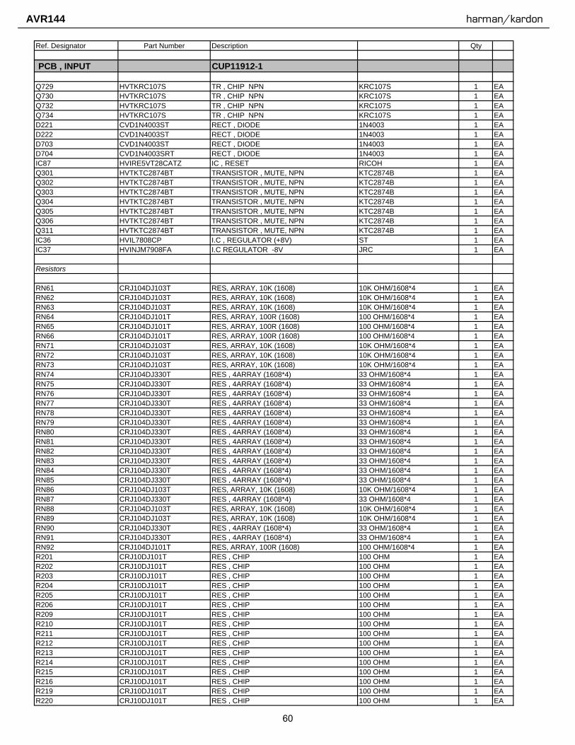
Ref. Designator Part Number Description Qty
PCB , INPUT CUP11912-1
Q729 HVTKRC107S TR , CHIP NPN KRC107S 1 EAQ730 HVTKRC107S TR , CHIP NPN KRC107S 1 EAQ732 HVTKRC107S TR , CHIP NPN KRC107S 1 EAQ734 HVTKRC107S TR , CHIP NPN KRC107S 1 EAD221 CVD1N4003ST RECT , DIODE 1N4003 1 EAD222 CVD1N4003ST RECT , DIODE 1N4003 1 EAD703 CVD1N4003ST RECT , DIODE 1N4003 1 EAD704 CVD1N4003SRT RECT , DIODE 1N4003 1 EAIC87 HVIRE5VT28CATZ IC , RESET RICOH 1 EAQ301 HVTKTC2874BT TRANSISTOR , MUTE, NPN KTC2874B 1 EAQ302 HVTKTC2874BT TRANSISTOR , MUTE, NPN KTC2874B 1 EAQ303 HVTKTC2874BT TRANSISTOR , MUTE, NPN KTC2874B 1 EAQ304 HVTKTC2874BT TRANSISTOR , MUTE, NPN KTC2874B 1 EAQ305 HVTKTC2874BT TRANSISTOR , MUTE, NPN KTC2874B 1 EAQ306 HVTKTC2874BT TRANSISTOR , MUTE, NPN KTC2874B 1 EAQ311 HVTKTC2874BT TRANSISTOR , MUTE, NPN KTC2874B 1 EAIC36 HVIL7808CP I.C , REGULATOR (+8V) ST 1 EAIC37 HVINJM7908FA I.C REGULATOR -8V JRC 1 EA
Resistors
RN61 CRJ104DJ103T RES, ARRAY, 10K (1608) 10K OHM/1608*4 1 EARN62 CRJ104DJ103T RES, ARRAY, 10K (1608) 10K OHM/1608*4 1 EARN63 CRJ104DJ103T RES, ARRAY, 10K (1608) 10K OHM/1608*4 1 EARN64 CRJ104DJ101T RES, ARRAY, 100R (1608) 100 OHM/1608*4 1 EARN65 CRJ104DJ101T RES, ARRAY, 100R (1608) 100 OHM/1608*4 1 EARN66 CRJ104DJ101T RES, ARRAY, 100R (1608) 100 OHM/1608*4 1 EARN71 CRJ104DJ103T RES, ARRAY, 10K (1608) 10K OHM/1608*4 1 EARN72 CRJ104DJ103T RES, ARRAY, 10K (1608) 10K OHM/1608*4 1 EARN73 CRJ104DJ103T RES, ARRAY, 10K (1608) 10K OHM/1608*4 1 EARN74 CRJ104DJ330T RES , 4ARRAY (1608*4) 33 OHM/1608*4 1 EARN75 CRJ104DJ330T RES , 4ARRAY (1608*4) 33 OHM/1608*4 1 EARN76 CRJ104DJ330T RES , 4ARRAY (1608*4) 33 OHM/1608*4 1 EARN77 CRJ104DJ330T RES , 4ARRAY (1608*4) 33 OHM/1608*4 1 EARN78 CRJ104DJ330T RES , 4ARRAY (1608*4) 33 OHM/1608*4 1 EARN79 CRJ104DJ330T RES , 4ARRAY (1608*4) 33 OHM/1608*4 1 EARN80 CRJ104DJ330T RES , 4ARRAY (1608*4) 33 OHM/1608*4 1 EARN81 CRJ104DJ330T RES , 4ARRAY (1608*4) 33 OHM/1608*4 1 EARN82 CRJ104DJ330T RES , 4ARRAY (1608*4) 33 OHM/1608*4 1 EARN83 CRJ104DJ330T RES , 4ARRAY (1608*4) 33 OHM/1608*4 1 EARN84 CRJ104DJ330T RES , 4ARRAY (1608*4) 33 OHM/1608*4 1 EARN85 CRJ104DJ330T RES , 4ARRAY (1608*4) 33 OHM/1608*4 1 EARN86 CRJ104DJ103T RES, ARRAY, 10K (1608) 10K OHM/1608*4 1 EARN87 CRJ104DJ330T RES , 4ARRAY (1608*4) 33 OHM/1608*4 1 EARN88 CRJ104DJ103T RES, ARRAY, 10K (1608) 10K OHM/1608*4 1 EARN89 CRJ104DJ103T RES, ARRAY, 10K (1608) 10K OHM/1608*4 1 EARN90 CRJ104DJ330T RES , 4ARRAY (1608*4) 33 OHM/1608*4 1 EARN91 CRJ104DJ330T RES , 4ARRAY (1608*4) 33 OHM/1608*4 1 EARN92 CRJ104DJ101T RES, ARRAY, 100R (1608) 100 OHM/1608*4 1 EAR201 CRJ10DJ101T RES , CHIP 100 OHM 1 EAR202 CRJ10DJ101T RES , CHIP 100 OHM 1 EAR203 CRJ10DJ101T RES , CHIP 100 OHM 1 EAR204 CRJ10DJ101T RES , CHIP 100 OHM 1 EAR205 CRJ10DJ101T RES , CHIP 100 OHM 1 EAR206 CRJ10DJ101T RES , CHIP 100 OHM 1 EAR209 CRJ10DJ101T RES , CHIP 100 OHM 1 EAR210 CRJ10DJ101T RES , CHIP 100 OHM 1 EAR211 CRJ10DJ101T RES , CHIP 100 OHM 1 EAR212 CRJ10DJ101T RES , CHIP 100 OHM 1 EAR213 CRJ10DJ101T RES , CHIP 100 OHM 1 EAR214 CRJ10DJ101T RES , CHIP 100 OHM 1 EAR215 CRJ10DJ101T RES , CHIP 100 OHM 1 EAR216 CRJ10DJ101T RES , CHIP 100 OHM 1 EAR219 CRJ10DJ101T RES , CHIP 100 OHM 1 EAR220 CRJ10DJ101T RES , CHIP 100 OHM 1 EA
60
AVR144 harman/kardon
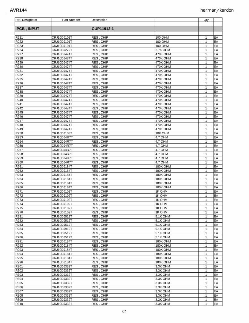
Ref. Designator Part Number Description Qty
PCB , INPUT CUP11912-1
R221 CRJ10DJ101T RES , CHIP 100 OHM 1 EAR222 CRJ10DJ101T RES , CHIP 100 OHM 1 EAR223 CRJ10DJ101T RES , CHIP 100 OHM 1 EAR224 CRJ10DJ272T RES , CHIP 2.7K OHM 1 EAR227 CRJ10DJ474T RES , CHIP 470K OHM 1 EAR228 CRJ10DJ474T RES , CHIP 470K OHM 1 EAR229 CRJ10DJ474T RES , CHIP 470K OHM 1 EAR230 CRJ10DJ474T RES , CHIP 470K OHM 1 EAR231 CRJ10DJ474T RES , CHIP 470K OHM 1 EAR232 CRJ10DJ474T RES , CHIP 470K OHM 1 EAR235 CRJ10DJ474T RES , CHIP 470K OHM 1 EAR236 CRJ10DJ474T RES , CHIP 470K OHM 1 EAR237 CRJ10DJ474T RES , CHIP 470K OHM 1 EAR238 CRJ10DJ474T RES , CHIP 470K OHM 1 EAR239 CRJ10DJ474T RES , CHIP 470K OHM 1 EAR240 CRJ10DJ474T RES , CHIP 470K OHM 1 EAR241 CRJ10DJ474T RES , CHIP 470K OHM 1 EAR242 CRJ10DJ474T RES , CHIP 470K OHM 1 EAR245 CRJ10DJ474T RES , CHIP 470K OHM 1 EAR246 CRJ10DJ474T RES , CHIP 470K OHM 1 EAR247 CRJ10DJ474T RES , CHIP 470K OHM 1 EAR248 CRJ10DJ474T RES , CHIP 470K OHM 1 EAR249 CRJ10DJ474T RES , CHIP 470K OHM 1 EAR250 CRJ10DJ103T RES , CHIP 10K OHM 1 EAR253 CRJ10DJ4R7T RES , CHIP 4.7 OHM 1 EAR254 CRJ10DJ4R7T RES , CHIP 4.7 OHM 1 EAR256 CRJ10DJ4R7T RES , CHIP 4.7 OHM 1 EAR257 CRJ10DJ4R7T RES , CHIP 4.7 OHM 1 EAR258 CRJ10DJ4R7T RES , CHIP 4.7 OHM 1 EAR259 CRJ10DJ4R7T RES , CHIP 4.7 OHM 1 EAR260 CRJ10DJ4R7T RES , CHIP 4.7 OHM 1 EAR261 CRJ10DJ184T RES , CHIP 180K OHM 1 EAR262 CRJ10DJ184T RES , CHIP 180K OHM 1 EAR263 CRJ10DJ184T RES , CHIP 180K OHM 1 EAR264 CRJ10DJ184T RES , CHIP 180K OHM 1 EAR265 CRJ10DJ184T RES , CHIP 180K OHM 1 EAR266 CRJ10DJ184T RES , CHIP 180K OHM 1 EAR271 CRJ10DJ102T RES , CHIP 1K OHM 1 EAR272 CRJ10DJ102T RES , CHIP 1K OHM 1 EAR273 CRJ10DJ102T RES , CHIP 1K OHM 1 EAR274 CRJ10DJ102T RES , CHIP 1K OHM 1 EAR275 CRJ10DJ102T RES , CHIP 1K OHM 1 EAR276 CRJ10DJ102T RES , CHIP 1K OHM 1 EAR281 CRJ10DJ512T RES , CHIP 5.1K OHM 1 EAR282 CRJ10DJ512T RES , CHIP 5.1K OHM 1 EAR283 CRJ10DJ512T RES , CHIP 5.1K OHM 1 EAR284 CRJ10DJ912T RES , CHIP 9.1K OHM 1 EAR285 CRJ10DJ512T RES , CHIP 5.1K OHM 1 EAR286 CRJ10DJ512T RES , CHIP 5.1K OHM 1 EAR291 CRJ10DJ184T RES , CHIP 180K OHM 1 EAR292 CRJ10DJ184T RES , CHIP 180K OHM 1 EAR293 CRJ10DJ184T RES , CHIP 180K OHM 1 EAR294 CRJ10DJ184T RES , CHIP 180K OHM 1 EAR295 CRJ10DJ184T RES , CHIP 180K OHM 1 EAR296 CRJ10DJ184T RES , CHIP 180K OHM 1 EAR301 CRJ10DJ332T RES , CHIP 3.3K OHM 1 EAR302 CRJ10DJ332T RES , CHIP 3.3K OHM 1 EAR303 CRJ10DJ332T RES , CHIP 3.3K OHM 1 EAR304 CRJ10DJ332T RES , CHIP 3.3K OHM 1 EAR305 CRJ10DJ332T RES , CHIP 3.3K OHM 1 EAR306 CRJ10DJ332T RES , CHIP 3.3K OHM 1 EAR307 CRJ10DJ332T RES , CHIP 3.3K OHM 1 EAR308 CRJ10DJ332T RES , CHIP 3.3K OHM 1 EAR309 CRJ10DJ332T RES , CHIP 3.3K OHM 1 EAR310 CRJ10DJ332T RES , CHIP 3.3K OHM 1 EA
61
AVR144 harman/kardon

Ref. Designator Part Number Description Qty
PCB , INPUT CUP11912-1
R311 CRJ10DJ332T RES , CHIP 3.3K OHM 1 EAR312 CRJ10DJ332T RES , CHIP 3.3K OHM 1 EAR317 CRJ10DJ561T RES , CHIP 560 OHM 1 EAR318 CRJ10DF3920T RES. CHIP (392R 1%) 392 OHM 1 EAR321 CRJ10DJ512T RES , CHIP 5.1K OHM 1 EAR322 CRJ10DJ122T RES , CHIP 1.2K OHM 1 EAR323 CRJ10DJ122T RES , CHIP 1.2K OHM 1 EAR324 CRJ10DJ512T RES , CHIP 5.1K OHM 1 EAR325 CRJ10DJ512T RES , CHIP 5.1K OHM 1 EAR326 CRJ10DJ122T RES , CHIP 1.2K OHM 1 EAR327 CRJ10DJ122T RES , CHIP 1.2K OHM 1 EAR328 CRJ10DJ103T RES , CHIP 10K OHM 1 EAR329 CRJ10DJ512T RES , CHIP 5.1K OHM 1 EAR330 CRJ10DJ122T RES , CHIP 1.2K OHM 1 EAR331 CRJ10DJ122T RES , CHIP 1.2K OHM 1 EAR332 CRJ10DJ512T RES , CHIP 5.1K OHM 1 EAR341 CRJ10DJ122T RES , CHIP 1.2K OHM 1 EAR344 CRJ10DJ122T RES , CHIP 1.2K OHM 1 EAR345 CRJ10DJ122T RES , CHIP 1.2K OHM 1 EAR348 CRJ10DJ122T RES , CHIP 1.2K OHM 1 EAR349 CRJ10DJ122T RES , CHIP 1.2K OHM 1 EAR352 CRJ10DJ122T RES , CHIP 1.2K OHM 1 EAR361 CRJ10DJ104T RES , CHIP 100K OHM 1 EAR362 CRJ10DJ104T RES , CHIP 100K OHM 1 EAR363 CRJ10DJ104T RES , CHIP 100K OHM 1 EAR364 CRJ10DJ104T RES , CHIP 100K OHM 1 EAR365 CRJ10DJ104T RES , CHIP 100K OHM 1 EAR366 CRJ10DJ104T RES , CHIP 100K OHM 1 EAR371 CRJ10DJ512T RES , CHIP 5.1K OHM 1 EAR372 CRJ10DJ512T RES , CHIP 5.1K OHM 1 EAR373 CRJ10DJ512T RES , CHIP 5.1K OHM 1 EAR374 CRJ10DJ103T RES , CHIP 10K OHM 1 EAR375 CRJ10DJ512T RES , CHIP 5.1K OHM 1 EAR376 CRJ10DJ512T RES , CHIP 5.1K OHM 1 EAR381 CRJ10DJ561T RES , CHIP 560 OHM 1 EAR382 CRJ10DJ561T RES , CHIP 560 OHM 1 EAR383 CRJ10DJ561T RES , CHIP 560 OHM 1 EAR384 CRJ10DJ561T RES , CHIP 560 OHM 1 EAR385 CRJ10DJ561T RES , CHIP 560 OHM 1 EAR386 CRJ10DJ561T RES , CHIP 560 OHM 1 EAR389 CRJ10DJ184T RES , CHIP 180K OHM 1 EAR390 CRJ10DJ184T RES , CHIP 180K OHM 1 EAR391 CRJ10DF3920T RES. CHIP (392R 1%) 392 OHM 1 EAR392 CRJ10DF3920T RES. CHIP (392R 1%) 392 OHM 1 EAR393 CRJ10DF3920T RES. CHIP (392R 1%) 392 OHM 1 EAR394 CRJ10DF3920T RES. CHIP (392R 1%) 392 OHM 1 EAR395 CRJ10DF3920T RES. CHIP (392R 1%) 392 OHM 1 EAR396 CRJ10DF3920T RES. CHIP (392R 1%) 392 OHM 1 EAR701 CRJ10DJ103T RES , CHIP 10K OHM 1 EAR702 CRJ10DJ103T RES , CHIP 10K OHM 1 EAR709 CRJ10DJ103T RES , CHIP 10K OHM 1 EAR710 CRJ10DJ103T RES , CHIP 10K OHM 1 EAR714 CRJ10DJ104T RES , CHIP 100K OHM 1 EAR715 CRJ10DJ104T RES , CHIP 100K OHM 1 EAR716 CRJ10DJ472T RES , CHIP 4.7K OHM 1 EAR717 CRJ10DJ3R3T RES , CHIP 3.3 OHM 1 EAR718 CRJ10DJ123T RES , CHIP 12K OHM 1 EAR719 CRJ10DJ473T RES , CHIP 47K OHM 1 EAR720 CRJ10DJ473T RES , CHIP 47K OHM 1 EAR721 CRJ10DJ330T RES , CHIP 33 OHM 1 EAR723 CRJ10DJ2R7T RES , CHIP 2.7 OHM 1 EAR724 CRJ10DJ101T RES , CHIP 100 OHM 1 EAR725 CRJ10DJ473T RES , CHIP 47K OHM 1 EAR726 CRJ10DJ473T RES , CHIP 47K OHM 1 EAR727 CRJ10DJ473T RES , CHIP 47K OHM 1 EA
62
AVR144 harman/kardon

Ref. Designator Part Number Description Qty
PCB , INPUT CUP11912-1
R728 CRJ10DJ102T RES , CHIP 1K OHM 1 EAR729 CRJ10DJ123T RES , CHIP 12K OHM 1 EAR730 CRJ10DJ123T RES , CHIP 12K OHM 1 EAR737 CRJ10DJ330T RES , CHIP 33 OHM 1 EAR739 CRJ10DJ1R0T RES , CHIP 1 OHM 1 EAR740 CRJ10DJ820T RES , CHIP 820 OHM 1 EAR741 CRJ10DJ330T RES , CHIP 820 OHM 1 EAR742 CRJ10DJ330T RES , CHIP 33 OHM 1 EAR743 CRJ10DJ330T RES , CHIP 33 OHM 1 EAR744 CRJ10DJ0R0T RES , CHIP 0 OHM 1 EAR746 CRJ10DJ0R0T RES , CHIP 0 OHM 1 EAR747 CRJ10DJ330T RES , CHIP 33 OHM 1 EAR748 CRJ10DJ330T RES , CHIP 33 OHM 1 EAR751 CRJ10DJ330T RES , CHIP 33 OHM 1 EAR752 CRJ10DJ330T RES , CHIP 33 OHM 1 EAR753 CRJ10DJ103T RES , CHIP 10K OHM 1 EAR754 CRJ10DJ103T RES , CHIP 10K OHM 1 EAR756 CRJ10DJ103T RES , CHIP 10K OHM 1 EAR759 CRJ10DJ330T RES , CHIP 33 OHM 1 EAR760 CRJ10DJ105T RES , CHIP 1M OHM 1 EAR765 CRJ10DJ103T RES , CHIP 10K OHM 1 EAR766 CRJ10DJ103T RES , CHIP 10K OHM 1 EAR767 CRJ10DJ301T RES , CHIP 300 OHM 1 EAR768 CRJ10DJ562T RES , CHIP 5.6K OHM 1 EAR773 CRJ10DJ332T RES , CHIP 10 OHM 1 EAR774 CRJ10DJ332T RES , CHIP 10K OHM 1 EAR775 CRJ10DJ332T RES , CHIP 47K OHM 1 EAR776 CRJ10DJ332T RES , CHIP 3.3K OHM 1 EAR777 CRJ10DJ102T RES , CHIP 1K OHM 1 EAR778 CRJ10DJ103T RES , CHIP 10K OHM 1 EAR782 CRJ10DJ272T RES , CHIP 2.7K OHM 1 EAR783 CRJ10DJ272T RES , CHIP 2.7K OHM 1 EAR784 CRJ10DJ473T RES , CHIP 47K OHM 1 EAR785 CRJ10DJ104T RES , CHIP 100K OHM 1 EAR786 CRJ10DJ471T RES , CHIP 470 OHM 1 EAR787 CRJ10DJ103T RES , CHIP 10K OHM 1 EAR788 CRJ10DJ103T RES , CHIP 10K OHM 1 EAR789 CRJ10DJ103T RES , CHIP 10K OHM 1 EAR790 CRJ10DJ103T RES , CHIP 10K OHM 1 EAR793 CRJ10DJ103T RES , CHIP 10K OHM 1 EAR794 CRJ10DJ102T RES , CHIP 1K OHM 1 EAR795 CRJ10DJ102T RES , CHIP 1K OHM 1 EAR796 CRJ10DJ102T RES , CHIP 1K OHM 1 EAR712 CRD20TJ103T RES , CARBON 10K OHM 1/5W J 1 EAR732 CRD20TJ103T RES , CARBON 10K OHM 1/5W J 1 EA
Miscellaneous
X702 HOX27000E180S CRYSTAL , CHIP(27MHZ,SMD) 27MHZ 1 EAL701 HLZ9Z014Z CHIP , BEAD HU-1H4516-600JT 1 EAL702 HLZ9Z014Z CHIP , BEAD HU-1H4516-600JT 1 EAL703 HLZ9Z014Z CHIP , BEAD HU-1H4516-600JT 1 EAL704 HLZ9R005Z BEAD CHIP 60(1608 SIZE) HH-1M1608-600 1 EAL705 HLZ9R005Z BEAD CHIP 60(1608 SIZE) HH-1M1608-600 1 EACN10 CJP04GB46ZY WAFER WAFER 1 EACN11 CJP13GA117ZY WAFER , CARD CABLE WAFER 1 EACN12 CJP21GA115ZY WAFER , CARD CABLE WAFER 1 EACN13 CJP13GA115ZY WAFER , CARD CABLE WAFER 1 EACN14 CJP09GA117ZY WAFER WAFER 1 EACN17 KJP12GB142ZP PIN HEADER WAFER 1 EACN18 CJP05GA19ZY WAFER, STRAIGHT, 5PIN WAFER 1 EACN19 CJP09GA117ZY WAFER WAFER 1 EACN20 CJP05GA01ZY CON WAFER YMW025-05R WAFER 1 EACN22 CJP06GA19ZY WAFER, STRAIGHT, 6PIN WAFER 1 EACN72 CJP17GA117ZY WAFER WAFER 1 EA
63
AVR144 harman/kardon
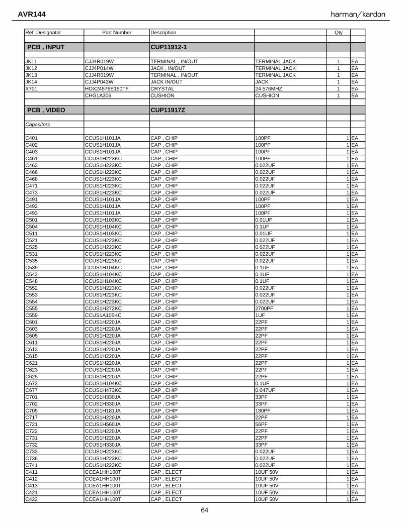
Ref. Designator Part Number Description Qty
PCB , INPUT CUP11912-1
JK11 CJJ4R019W TERMINAL , IN/OUT TERMINAL JACK 1 EAJK12 CJJ4P014W JACK , IN/OUT TERMINAL JACK 1 EAJK13 CJJ4R019W TERMINAL , IN/OUT TERMINAL JACK 1 EAJK14 CJJ4P043W JACK IN/OUT JACK 1 EAX701 HOX24576E150TF CRYSTAL 24.576MHZ 1 EA
CHG1A306 CUSHION CUSHION 1 EA
PCB , VIDEO CUP11917Z
Capacitors
C401 CCUS1H101JA CAP , CHIP 100PF 1 EAC402 CCUS1H101JA CAP , CHIP 100PF 1 EAC403 CCUS1H101JA CAP , CHIP 100PF 1 EAC461 CCUS1H223KC CAP , CHIP 100PF 1 EAC463 CCUS1H223KC CAP , CHIP 0.022UF 1 EAC466 CCUS1H223KC CAP , CHIP 0.022UF 1 EAC468 CCUS1H223KC CAP , CHIP 0.022UF 1 EAC471 CCUS1H223KC CAP , CHIP 0.022UF 1 EAC473 CCUS1H223KC CAP , CHIP 0.022UF 1 EAC491 CCUS1H101JA CAP , CHIP 100PF 1 EAC492 CCUS1H101JA CAP , CHIP 100PF 1 EAC493 CCUS1H101JA CAP , CHIP 100PF 1 EAC501 CCUS1H103KC CAP , CHIP 0.01UF 1 EAC504 CCUS1H104KC CAP , CHIP 0.1UF 1 EAC511 CCUS1H103KC CAP , CHIP 0.01UF 1 EAC521 CCUS1H223KC CAP , CHIP 0.022UF 1 EAC525 CCUS1H223KC CAP , CHIP 0.022UF 1 EAC531 CCUS1H223KC CAP , CHIP 0.022UF 1 EAC535 CCUS1H223KC CAP , CHIP 0.022UF 1 EAC539 CCUS1H104KC CAP , CHIP 0.1UF 1 EAC543 CCUS1H104KC CAP , CHIP 0.1UF 1 EAC548 CCUS1H104KC CAP , CHIP 0.1UF 1 EAC552 CCUS1H223KC CAP , CHIP 0.022UF 1 EAC553 CCUS1H223KC CAP , CHIP 0.022UF 1 EAC554 CCUS1H223KC CAP , CHIP 0.022UF 1 EAC555 CCUS1H272KC CAP , CHIP 2700PF 1 EAC559 CCUS1A105KC CAP , CHIP 1UF 1 EAC601 CCUS1H220JA CAP , CHIP 22PF 1 EAC603 CCUS1H220JA CAP , CHIP 22PF 1 EAC605 CCUS1H220JA CAP , CHIP 22PF 1 EAC611 CCUS1H220JA CAP , CHIP 22PF 1 EAC613 CCUS1H220JA CAP , CHIP 22PF 1 EAC615 CCUS1H220JA CAP , CHIP 22PF 1 EAC621 CCUS1H220JA CAP , CHIP 22PF 1 EAC623 CCUS1H220JA CAP , CHIP 22PF 1 EAC625 CCUS1H220JA CAP , CHIP 22PF 1 EAC672 CCUS1H104KC CAP , CHIP 0.1UF 1 EAC677 CCUS1H473KC CAP , CHIP 0.047UF 1 EAC701 CCUS1H330JA CAP , CHIP 33PF 1 EAC702 CCUS1H330JA CAP , CHIP 33PF 1 EAC705 CCUS1H181JA CAP , CHIP 180PF 1 EAC717 CCUS1H220JA CAP , CHIP 22PF 1 EAC721 CCUS1H560JA CAP , CHIP 56PF 1 EAC722 CCUS1H220JA CAP , CHIP 22PF 1 EAC731 CCUS1H220JA CAP , CHIP 22PF 1 EAC732 CCUS1H330JA CAP , CHIP 33PF 1 EAC733 CCUS1H223KC CAP , CHIP 0.022UF 1 EAC736 CCUS1H223KC CAP , CHIP 0.022UF 1 EAC741 CCUS1H223KC CAP , CHIP 0.022UF 1 EAC411 CCEA1HH100T CAP , ELECT 10UF 50V 1 EAC412 CCEA1HH100T CAP , ELECT 10UF 50V 1 EAC413 CCEA1HH100T CAP , ELECT 10UF 50V 1 EAC421 CCEA1HH100T CAP , ELECT 10UF 50V 1 EAC422 CCEA1HH100T CAP , ELECT 10UF 50V 1 EA
64
AVR144 harman/kardon
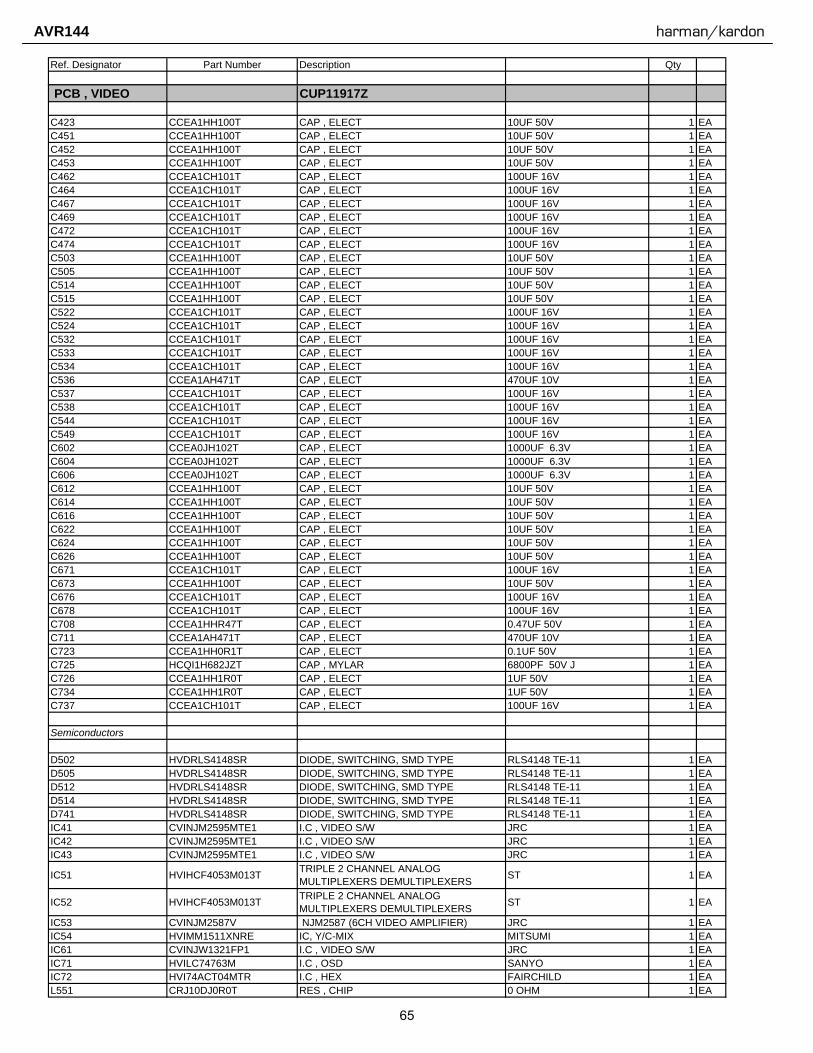
Ref. Designator Part Number Description Qty
PCB , VIDEO CUP11917Z
C423 CCEA1HH100T CAP , ELECT 10UF 50V 1 EAC451 CCEA1HH100T CAP , ELECT 10UF 50V 1 EAC452 CCEA1HH100T CAP , ELECT 10UF 50V 1 EAC453 CCEA1HH100T CAP , ELECT 10UF 50V 1 EAC462 CCEA1CH101T CAP , ELECT 100UF 16V 1 EAC464 CCEA1CH101T CAP , ELECT 100UF 16V 1 EAC467 CCEA1CH101T CAP , ELECT 100UF 16V 1 EAC469 CCEA1CH101T CAP , ELECT 100UF 16V 1 EAC472 CCEA1CH101T CAP , ELECT 100UF 16V 1 EAC474 CCEA1CH101T CAP , ELECT 100UF 16V 1 EAC503 CCEA1HH100T CAP , ELECT 10UF 50V 1 EAC505 CCEA1HH100T CAP , ELECT 10UF 50V 1 EAC514 CCEA1HH100T CAP , ELECT 10UF 50V 1 EAC515 CCEA1HH100T CAP , ELECT 10UF 50V 1 EAC522 CCEA1CH101T CAP , ELECT 100UF 16V 1 EAC524 CCEA1CH101T CAP , ELECT 100UF 16V 1 EAC532 CCEA1CH101T CAP , ELECT 100UF 16V 1 EAC533 CCEA1CH101T CAP , ELECT 100UF 16V 1 EAC534 CCEA1CH101T CAP , ELECT 100UF 16V 1 EAC536 CCEA1AH471T CAP , ELECT 470UF 10V 1 EAC537 CCEA1CH101T CAP , ELECT 100UF 16V 1 EAC538 CCEA1CH101T CAP , ELECT 100UF 16V 1 EAC544 CCEA1CH101T CAP , ELECT 100UF 16V 1 EAC549 CCEA1CH101T CAP , ELECT 100UF 16V 1 EAC602 CCEA0JH102T CAP , ELECT 1000UF 6.3V 1 EAC604 CCEA0JH102T CAP , ELECT 1000UF 6.3V 1 EAC606 CCEA0JH102T CAP , ELECT 1000UF 6.3V 1 EAC612 CCEA1HH100T CAP , ELECT 10UF 50V 1 EAC614 CCEA1HH100T CAP , ELECT 10UF 50V 1 EAC616 CCEA1HH100T CAP , ELECT 10UF 50V 1 EAC622 CCEA1HH100T CAP , ELECT 10UF 50V 1 EAC624 CCEA1HH100T CAP , ELECT 10UF 50V 1 EAC626 CCEA1HH100T CAP , ELECT 10UF 50V 1 EAC671 CCEA1CH101T CAP , ELECT 100UF 16V 1 EAC673 CCEA1HH100T CAP , ELECT 10UF 50V 1 EAC676 CCEA1CH101T CAP , ELECT 100UF 16V 1 EAC678 CCEA1CH101T CAP , ELECT 100UF 16V 1 EAC708 CCEA1HHR47T CAP , ELECT 0.47UF 50V 1 EAC711 CCEA1AH471T CAP , ELECT 470UF 10V 1 EAC723 CCEA1HH0R1T CAP , ELECT 0.1UF 50V 1 EAC725 HCQI1H682JZT CAP , MYLAR 6800PF 50V J 1 EAC726 CCEA1HH1R0T CAP , ELECT 1UF 50V 1 EAC734 CCEA1HH1R0T CAP , ELECT 1UF 50V 1 EAC737 CCEA1CH101T CAP , ELECT 100UF 16V 1 EA
Semiconductors
D502 HVDRLS4148SR DIODE, SWITCHING, SMD TYPE RLS4148 TE-11 1 EAD505 HVDRLS4148SR DIODE, SWITCHING, SMD TYPE RLS4148 TE-11 1 EAD512 HVDRLS4148SR DIODE, SWITCHING, SMD TYPE RLS4148 TE-11 1 EAD514 HVDRLS4148SR DIODE, SWITCHING, SMD TYPE RLS4148 TE-11 1 EAD741 HVDRLS4148SR DIODE, SWITCHING, SMD TYPE RLS4148 TE-11 1 EAIC41 CVINJM2595MTE1 I.C , VIDEO S/W JRC 1 EAIC42 CVINJM2595MTE1 I.C , VIDEO S/W JRC 1 EAIC43 CVINJM2595MTE1 I.C , VIDEO S/W JRC 1 EA
IC51 HVIHCF4053M013T TRIPLE 2 CHANNEL ANALOG MULTIPLEXERS DEMULTIPLEXERS ST 1 EA
IC52 HVIHCF4053M013T TRIPLE 2 CHANNEL ANALOG MULTIPLEXERS DEMULTIPLEXERS ST 1 EA
IC53 CVINJM2587V NJM2587 (6CH VIDEO AMPLIFIER) JRC 1 EAIC54 HVIMM1511XNRE IC, Y/C-MIX MITSUMI 1 EAIC61 CVINJW1321FP1 I.C , VIDEO S/W JRC 1 EAIC71 HVILC74763M I.C , OSD SANYO 1 EAIC72 HVI74ACT04MTR I.C , HEX FAIRCHILD 1 EAL551 CRJ10DJ0R0T RES , CHIP 0 OHM 1 EA
65
AVR144 harman/kardon
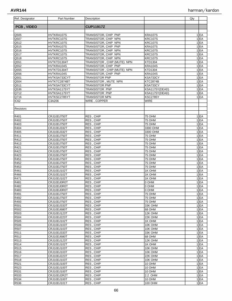
Ref. Designator Part Number Description Qty
PCB , VIDEO CUP11917Z
Q505 HVTKRA107S TRANSISTOR, CHIP PNP KRA107S 1 EAQ507 HVTKRC107S TRANSISTOR, CHIP NPN KRC107S 1 EAQ512 HVTKRC107S TRANSISTOR, CHIP NPN KRC107S 1 EAQ515 HVTKRA107S TRANSISTOR, CHIP PNP KRA107S 1 EAQ516 HVTKRC107S TRANSISTOR, CHIP NPN KRC107S 1 EAQ517 HVTKRC107S TRANSISTOR, CHIP NPN KRC107S 1 EAQ518 HVTKRC107S TRANSISTOR, CHIP NPN KRC107S 1 EAQ551 HVTKTD1304T TRANSISTOR , CHIP (MUTE) NPN KTD1304 1 EAQ552 HVTKRA104S TRANSISTOR, CHIP PNP KRA104S 1 EAQ555 HVTKTD1304T TRANSISTOR , CHIP (MUTE) NPN KTD1304 1 EAQ556 HVTKRA104S TRANSISTOR, CHIP PNP KRA104S 1 EAQ501 HVTKSA733CYT TRANSISTOR PNP KSA733CY 1 EAQ504 HVTKTC2874BT TRANSISTOR , MUTE NPN KTC2874B 1 EAQ511 HVTKSA733CYT TRANSISTOR PNP KSA733CY 1 EAQ536 HVTKSA1175YT TRANSISTOR PNP KSA1175Y(DEAD) 1 EAQ712 HVTKSA1175YT TRANSISTOR PNP KSA1175Y(DEAD) 1 EAQ716 HVTKSC2785YT TRANSISTOR NPN KSC2785Y 1 EAIC62 C3A206 WIRE , COPPER WIRE
Resistors
R401 CRJ10DJ750T RES , CHIP 75 OHM 1 EAR402 CRJ10DJ750T RES , CHIP 75 OHM 1 EAR403 CRJ10DJ750T RES , CHIP 75 OHM 1 EAR404 CRJ10DJ332T RES , CHIP 3300 OHM 1 EAR405 CRJ10DJ332T RES , CHIP 3300 OHM 1 EAR411 CRJ10DJ750T RES , CHIP 75 OHM 1 EAR412 CRJ10DJ750T RES , CHIP 75 OHM 1 EAR413 CRJ10DJ750T RES , CHIP 75 OHM 1 EAR421 CRJ10DJ750T RES , CHIP 75 OHM 1 EAR422 CRJ10DJ750T RES , CHIP 75 OHM 1 EAR423 CRJ10DJ750T RES , CHIP 75 OHM 1 EAR451 CRJ10DJ750T RES , CHIP 75 OHM 1 EAR452 CRJ10DJ750T RES , CHIP 75 OHM 1 EAR453 CRJ10DJ750T RES , CHIP 75 OHM 1 EAR461 CRJ10DJ102T RES , CHIP 1K OHM 1 EAR466 CRJ10DJ102T RES , CHIP 1K OHM 1 EAR471 CRJ10DJ102T RES , CHIP 1K OHM 1 EAR481 CRJ10DJ0R0T RES , CHIP 0 OHM 1 EAR482 CRJ10DJ0R0T RES , CHIP 0 OHM 1 EAR483 CRJ10DJ0R0T RES , CHIP 0 OHM 1 EAR491 CRJ10DJ750T RES , CHIP 75 OHM 1 EAR492 CRJ10DJ750T RES , CHIP 75 OHM 1 EAR493 CRJ10DJ750T RES , CHIP 75 OHM 1 EAR501 CRJ10DJ333T RES , CHIP 33K OHM 1 EAR502 CRJ10DJ680T RES , CHIP 68 OHM 1 EAR503 CRJ10DJ123T RES , CHIP 12K OHM 1 EAR504 CRJ10DJ223T RES , CHIP 22K OHM 1 EAR505 CRJ10DJ102T RES , CHIP 1K OHM 1 EAR506 CRJ10DJ103T RES , CHIP 10K OHM 1 EAR507 CRJ10DJ103T RES , CHIP 10K OHM 1 EAR511 CRJ10DJ333T RES , CHIP 33K OHM 1 EAR512 CRJ10DJ680T RES , CHIP 68 OHM 1 EAR513 CRJ10DJ123T RES , CHIP 12K OHM 1 EAR514 CRJ10DJ102T RES , CHIP 1K OHM 1 EAR515 CRJ10DJ103T RES , CHIP 10K OHM 1 EAR516 CRJ10DJ103T RES , CHIP 10K OHM 1 EAR517 CRJ10DJ223T RES , CHIP 22K OHM 1 EAR518 CRJ10DJ103T RES , CHIP 10K OHM 1 EAR521 CRJ10DJ100T RES , CHIP 10 OHM 1 EAR523 CRJ10DJ100T RES , CHIP 10 OHM 1 EAR531 CRJ10DJ100T RES , CHIP 10 OHM 1 EAR533 CRJ10DJ2R2T RES , CHIP 2.2 OHM 1 EAR534 CRJ10DJ100T RES , CHIP 10 OHM 1 EAR536 CRJ10DJ101T RES , CHIP 100 OHM 1 EA
66
AVR144 harman/kardon
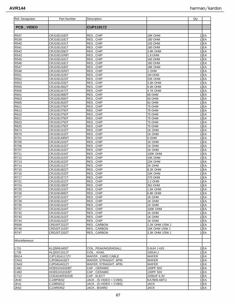
Ref. Designator Part Number Description Qty
PCB , VIDEO CUP11917Z
R537 CRJ10DJ183T RES , CHIP 18K OHM 1 EAR539 CRJ10DJ181T RES , CHIP 180 OHM 1 EAR540 CRJ10DJ101T RES , CHIP 100 OHM 1 EAR541 CRJ10DJ181T RES , CHIP 180 OHM 1 EAR542 CRJ10DJ392T RES . CHIP 3.9K OHM 1 EAR543 CRJ10DJ1R8T RES , CHIP 1.8 OHM 1 EAR545 CRJ10DJ161T RES , CHIP 160 OHM 1 EAR546 CRJ10DJ181T RES , CHIP 180 OHM 1 EAR547 CRJ10DJ183T RES , CHIP 18K OHM 1 EAR548 CRJ10DJ1R0T RES , CHIP 1 OHM 1 EAR551 CRJ10DJ105T RES , CHIP 1M OHM 1 EAR552 CRJ10DJ223T RES , CHIP 22K OHM 1 EAR553 CRJ10DJ332T RES , CHIP 3.3K OHM 1 EAR555 CRJ10DJ562T RES , CHIP 5.6K OHM 1 EAR556 CRJ10DJ472T RES , CHIP 4.7K OHM 1 EAR601 CRJ10DJ680T RES , CHIP 68 OHM 1 EAR603 CRJ10DJ560T RES , CHIP 56 OHM 1 EAR605 CRJ10DJ620T RES , CHIP 62 OHM 1 EAR611 CRJ10DJ750T RES , CHIP 75 OHM 1 EAR613 CRJ10DJ750T RES , CHIP 75 OHM 1 EAR615 CRJ10DJ750T RES , CHIP 75 OHM 1 EAR621 CRJ10DJ750T RES , CHIP 75 OHM 1 EAR623 CRJ10DJ750T RES , CHIP 75 OHM 1 EAR625 CRJ10DJ750T RES , CHIP 75 OHM 1 EAR674 CRJ10DJ102T RES , CHIP 1K OHM 1 EAR675 CRJ10DJ102T RES , CHIP 1K OHM 1 EAR701 CRJ10DJ0R0T RES , CHIP 0 OHM 1 EAR705 CRJ10DJ102T RES , CHIP 1K OHM 1 EAR706 CRJ10DJ102T RES , CHIP 1K OHM 1 EAR707 CRJ10DJ102T RES , CHIP 1K OHM 1 EAR711 CRJ10DJ104T RES , CHIP 100K OHM 1 EAR712 CRJ10DJ103T RES , CHIP 10K OHM 1 EAR713 CRJ10DJ223T RES , CHIP 22K OHM 1 EAR714 CRJ10DJ122T RES , CHIP 2K OHM 1 EAR715 CRJ10DJ822T RES , CHIP 8.2K OHM 1 EAR716 CRJ10DJ103T RES , CHIP 10K OHM 1 EAR717 CRJ10DJ271T RES , CHIP 270 OHM 1 EAR721 CRJ10DJ222T RES , CHIP 2.2 OHM 1 EAR724 CRJ10DJ393T RES , CHIP 39J OHM 1 EAR725 CRJ10DJ152T RES , CHIP 1.5K OHM 1 EAR726 CRJ10DJ682T RES , CHIP 6.8K OHM 1 EAR727 CRJ10DJ102T RES , CHIP 1K OHM 1 EAR728 CRJ10DJ102T RES , CHIP 1K OHM 1 EAR735 CRJ10DJ102T RES , CHIP 1K OHM 1 EAR737 CRJ10DJ104T RES , CHIP 100K OHM 1 EAR742 CRJ10DJ102T RES , CHIP 1K OHM 1 EAR743 CRJ10DJ102T RES , CHIP 1K OHM 1 EAR744 CRJ10DJ102T RES , CHIP 1K OHM 1 EAR558 CRD20TJ222T RES , CARBON 2.2K OHM 1/5W J 1 EAR746 CRD20TJ103T RES , CARBON 10K OHM 1/5W J 1 EAR747 CRD20TJ332T RES , CARBON 3.3K OHM 1/5W J 1 EA
Miscellaneous
L731 KLQ5R6J405T COIL, PEAKING(RADIAL) 5.6UH J 4X5 1 EAL736 HLQ02C101JT COIL , AXAIL 100UH,J 1 EABN14 CJP13GA117ZY WAFER , CARD CABLE WAFER 1 EACN41 CJP06GA19ZY WAFER, STRAIGHT, 6PIN WAFER 1 EACN43 CJP04GA01ZY WAFER, STRAIGHT, 4PIN WAFER 1 EAC481 HCBS1H101KBT CAP , CERAMIC 100PF 50V 1 EAC483 HCBS1H101KBT CAP , CERAMIC 100PF 50V 1 EAC712 CCEA0JKR3222E CAP , ELECT 2200UF 6.3V 1 EAJK40 CJJ9P003Z JACK , (S-VIDEO + CVBS) KA7809-ABTU 1 EAJK41 CJJ9R001Z JACK , (S-VIDEO + CVBS) JACK 1 EAJK62 CJJ4R045Z JACK , BOARD JACK 1 EA
67
AVR144 harman/kardon

Ref. Designator Part Number Description Qty
PCB , VIDEO CUP11917Z
JK69 CJJ4S030Z JACK , BOARD JACK 1 EAX701 HOX14318E220C CRYSTAL 14.318Mhz 1 EA
CNVM9011MS071L AVR 144 TUNER MODULE
68
AVR144 harman/kardon
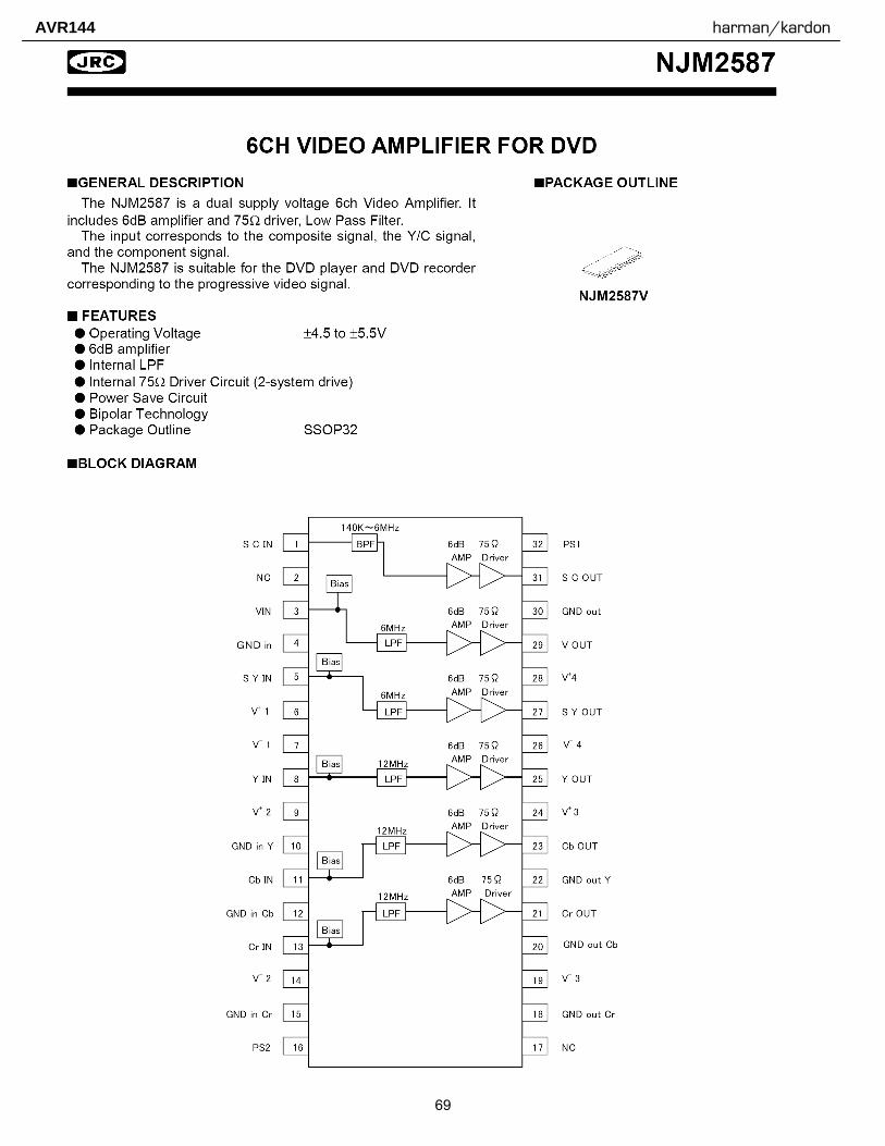
69
AVR144 harman/kardon

70
AVR144 harman/kardon
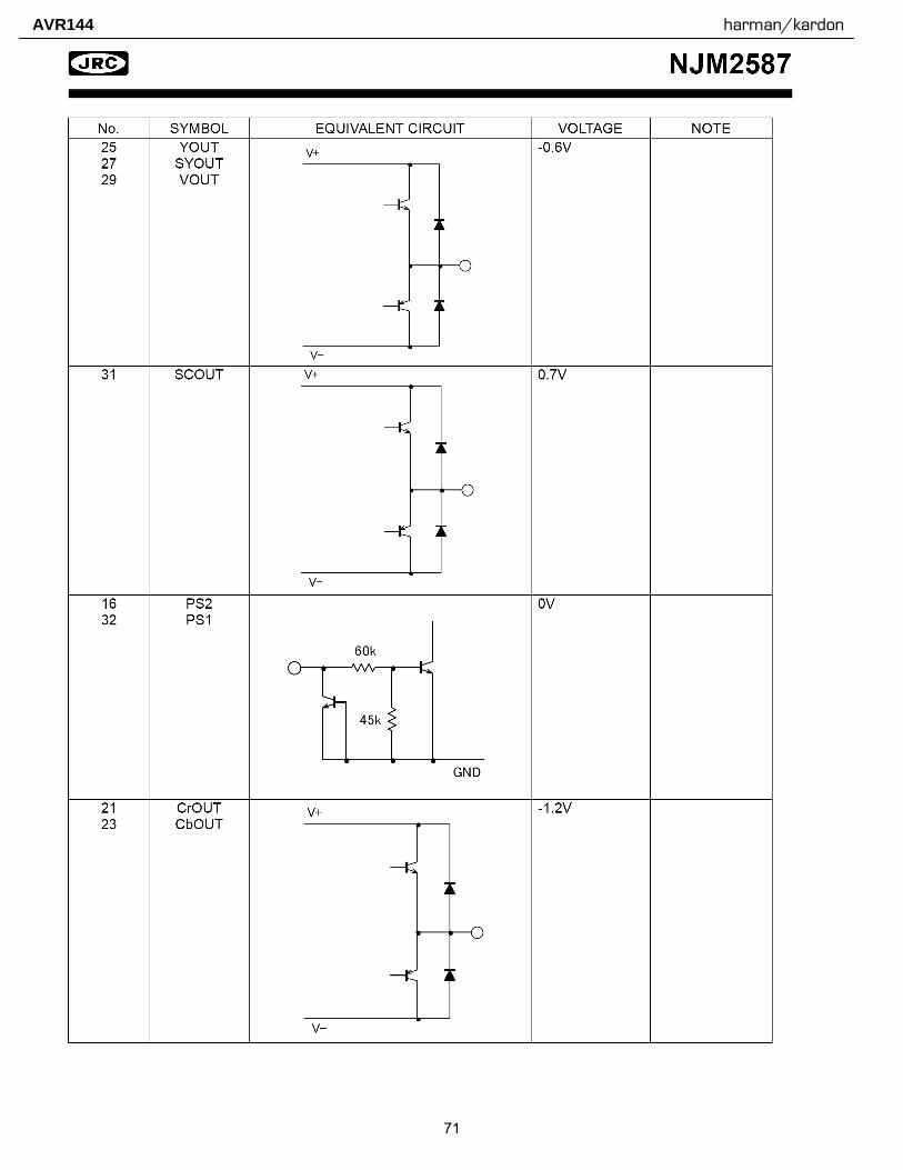
71
AVR144 harman/kardon
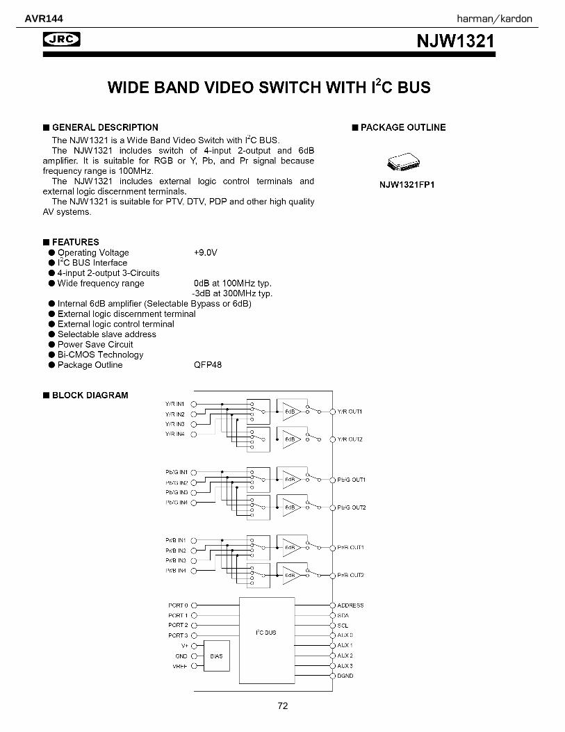
72
AVR144 harman/kardon
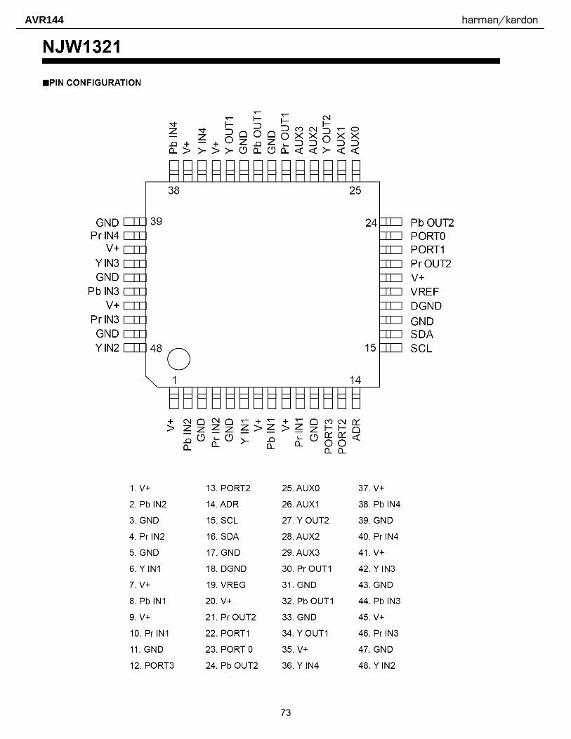
73
AVR144 harman/kardon
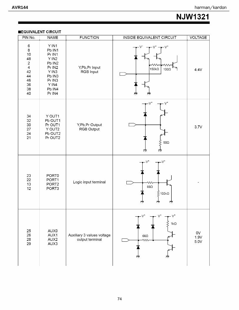
74
AVR144 harman/kardon

75
AVR144 harman/kardon
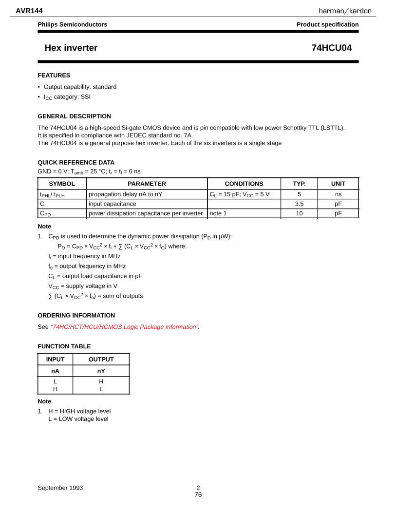
September 1993 2
Philips Semiconductors Product specification
Hex inverter 74HCU04
FEATURES
• Output capability: standard
• ICC category: SSI
GENERAL DESCRIPTION
The 74HCU04 is a high-speed Si-gate CMOS device and is pin compatible with low power Schottky TTL (LSTTL).It is specified in compliance with JEDEC standard no. 7A.The 74HCU04 is a general purpose hex inverter. Each of the six inverters is a single stage
QUICK REFERENCE DATAGND = 0 V; Tamb = 25 °C; tr = tf = 6 ns
Note
1. CPD is used to determine the dynamic power dissipation (PD in µW):
PD = CPD × VCC2 × fi + ∑ (CL × VCC
2 × fO) where:
fi = input frequency in MHz
fo = output frequency in MHz
CL = output load capacitance in pF
VCC = supply voltage in V
∑ (CL × VCC2 × fo) = sum of outputs
ORDERING INFORMATION
See “74HC/HCT/HCU/HCMOS Logic Package Information”.
FUNCTION TABLE
Note
1. H = HIGH voltage levelL = LOW voltage level
SYMBOL PARAMETER CONDITIONS TYP. UNIT
tPHL/ tPLH propagation delay nA to nY CL = 15 pF; VCC = 5 V 5 ns
CI input capacitance 3.5 pF
CPD power dissipation capacitance per inverter note 1 10 pF
INPUT OUTPUT
nA nY
LH
HL
76
AVR144 harman/kardon

September 1993 3
Philips Semiconductors Product specification
Hex inverter 74HCU04
PIN DESCRIPTION
PIN NO. SYMBOL NAME AND FUNCTION
1, 3, 5, 9, 11, 13 1A to 6A data inputs
2, 4, 6, 8, 10, 12 1Y to 6Y data outputs
7 GND ground (0 V)
14 VCC positive supply voltage
Fig.1 Pin configuration. Fig.2 Logic symbol. Fig.3 IEC logic symbol.
Fig.4 Functional diagram.Fig.5 Schematic diagram
(one inverter).
77
AVR144 harman/kardon
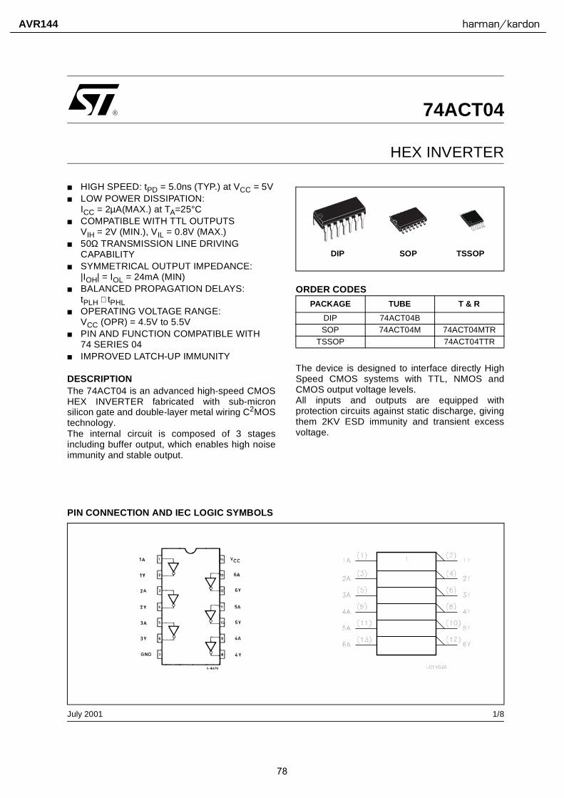
1/8July 2001
HIGH SPEED: tPD = 5.0ns (TYP.) at VCC = 5V LOW POWER DISSIPATION:
ICC = 2µA(MAX.) at TA=25°C COMPATIBLE WITH TTL OUTPUTS
VIH = 2V (MIN.), VIL = 0.8V (MAX.) 50Ω TRANSMISSION LINE DRIVING
CAPABILITY SYMMETRICAL OUTPUT IMPEDANCE:
|IOH| = IOL = 24mA (MIN) BALANCED PROPAGATION DELAYS:
tPLH ≅ tPHL OPERATING VOLTAGE RANGE:
VCC (OPR) = 4.5V to 5.5V PIN AND FUNCTION COMPATIBLE WITH
74 SERIES 04 IMPROVED LATCH-UP IMMUNITY
DESCRIPTIONThe 74ACT04 is an advanced high-speed CMOSHEX INVERTER fabricated with sub-micronsilicon gate and double-layer metal wiring C2MOStechnology. The internal circuit is composed of 3 stagesincluding buffer output, which enables high noiseimmunity and stable output.
The device is designed to interface directly HighSpeed CMOS systems with TTL, NMOS andCMOS output voltage levels.All inputs and outputs are equipped withprotection circuits against static discharge, givingthem 2KV ESD immunity and transient excessvoltage.
74ACT04
HEX INVERTER
PIN CONNECTION AND IEC LOGIC SYMBOLS
ORDER CODES
PACKAGE TUBE T & R
DIP 74ACT04B
SOP 74ACT04M 74ACT04MTR
TSSOP 74ACT04TTR
TSSOPDIP SOP
78
AVR144 harman/kardon

NJM2595
5-INPUT 3-OUTPUT VIDEO SWITCH
GENERAL DESCRIPTION PACKAGE OUTLINE
FEATURES
5-input 3-output Operating Voltage ±4.0 to ±6.5V Operating current ±15mAtyp. at Vcc=±5V Crosstalk -65dBtyp. Internal 6dB Amplifier Internal 75Ω Driver Bipolar Technology Package Outline DIP16,DMP16
PIN CONFIGURATION and BLOCK DIAGRAM
13
9
7
5
3
20k
20k
20k
20k
16 10 14 2
1
15
11
8 12 6 4
6dB Amp
75Ω Driver
S3
S2
S4
S1
20k
20k
20k
S5
S6
S7
Vin1
Vin2
Vin3
Vin4
Vin5
SW3 SW4
SW5 SW1 SW2V+
GND V-
Vout3
Vout2
Vout1
6dB Amp
6dB Amp
75Ω Driver
75Ω Driver
The NJM2595 is a 5-input 3-output video switch. Its switches select one from five signals received from VTR,TV,DVD, TV-GAME and others. The NJM2595 is designed for audio items, such as AV amplifier and others.
NJM2595D NJM2595M
79
AVR144 harman/kardon
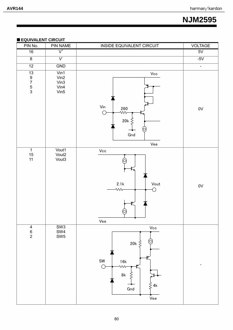
NJM2595
EQUIVALENT CIRCUIT PIN No. PIN NAME INSIDE EQUIVALENT CIRCUIT VOLTAGE
16 V+ 5V
8 V- -5V
12 GND - 13 9 7 5 3
Vin1 Vin2 Vin3 Vin4 Vin5
260
20k
Gnd
Vcc
Vee
Vin
0V
1 15 11
Vout1 Vout2 Vout3
Vcc
2.1k
Vee
Vout
0V
4 6 2
SW3 SW4 SW5
4k
16k
8k
Gnd
Vcc
Vee
SW
20k
-
80
AVR144 harman/kardon
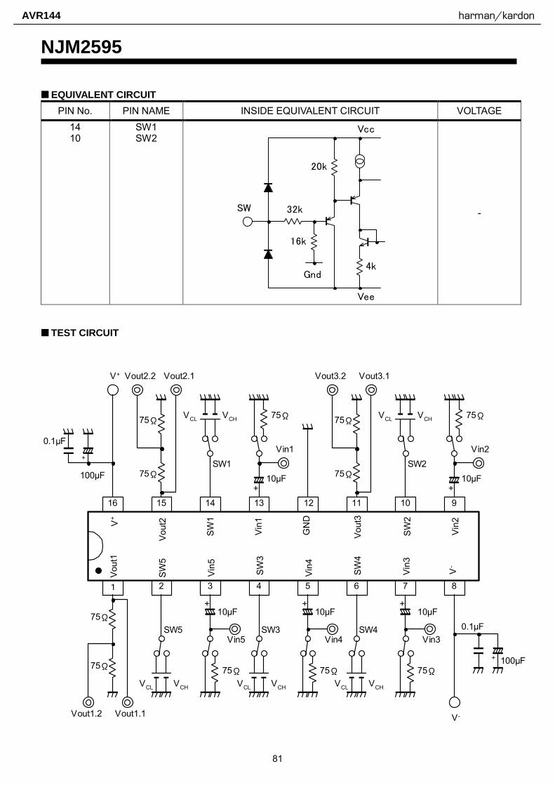
NJM2595
EQUIVALENT CIRCUIT PIN No. PIN NAME INSIDE EQUIVALENT CIRCUIT VOLTAGE
14 10
SW1 SW2
4k
32k
16k
Gnd
Vcc
Vee
SW
20k
-
TEST CIRCUIT
Vout3.1
+
Vin2
SW2
Vout
3
GN
D
Vin1
SW1
Vout
2V+
V-
Vin3
SW4
Vin4
SW3
Vin5
SW5
Vout
1
SW2
V+
Vin2
75Ω 10µF
1
9
8765432
16 15 14 13 12 11 10
+
75Ω
+
Vin1
10µF
75Ω 75Ω
Vout3.2
SW1
VCHVCLVCL VCH
75Ω
75Ω
Vout2.2 Vout2.1
V-
+
+
Vin3
10µF
75Ω
SW4
VCHVCL
+
Vin4
10µF
75Ω
SW3
VCHVCL
+
Vin5
10µF
75Ω
SW5
VCL VCH
75Ω
75Ω
Vout1.2 Vout1.1
0.1µF
100µF
0.1µF
100µF
81
AVR144 harman/kardon
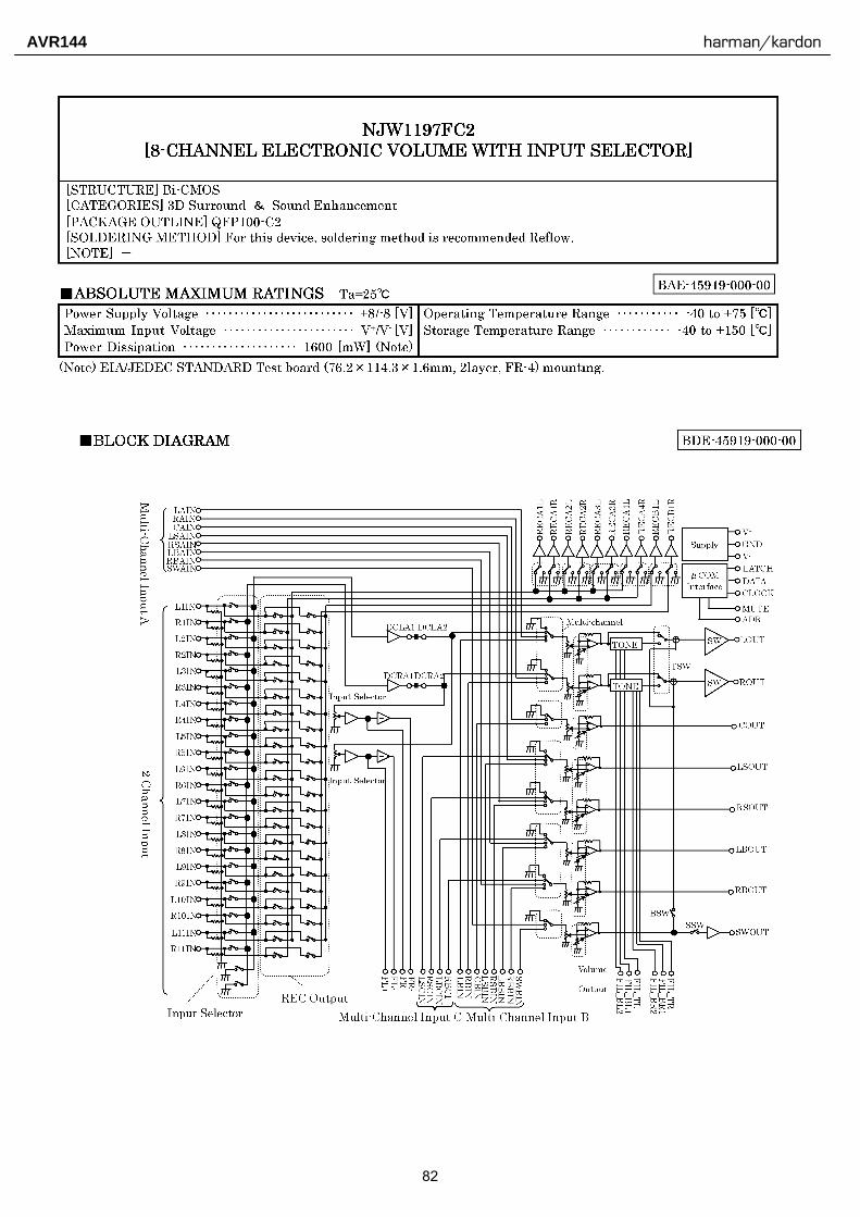
82
AVR144 harman/kardon
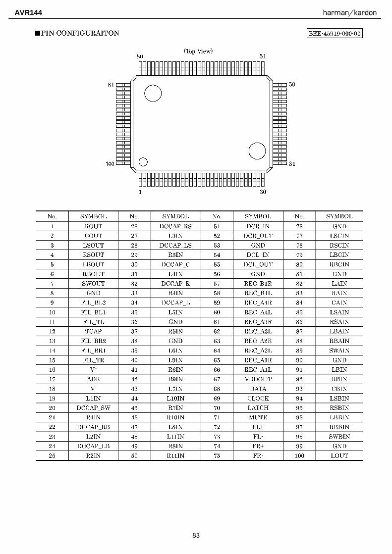
83
AVR144 harman/kardon

84
AVR144 harman/kardon
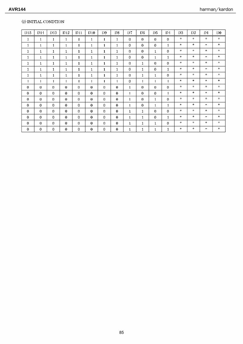
85
AVR144 harman/kardon
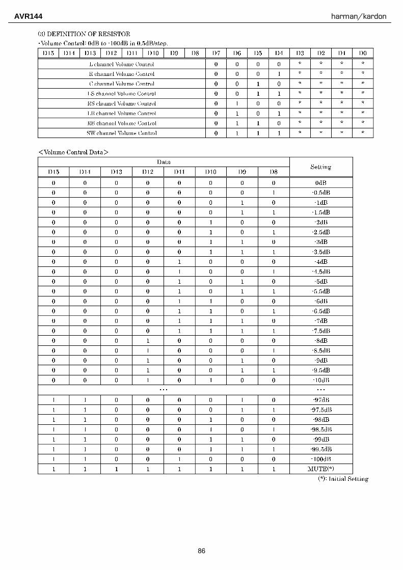
86
AVR144 harman/kardon
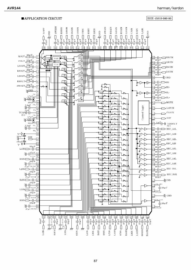
87
AVR144 harman/kardon
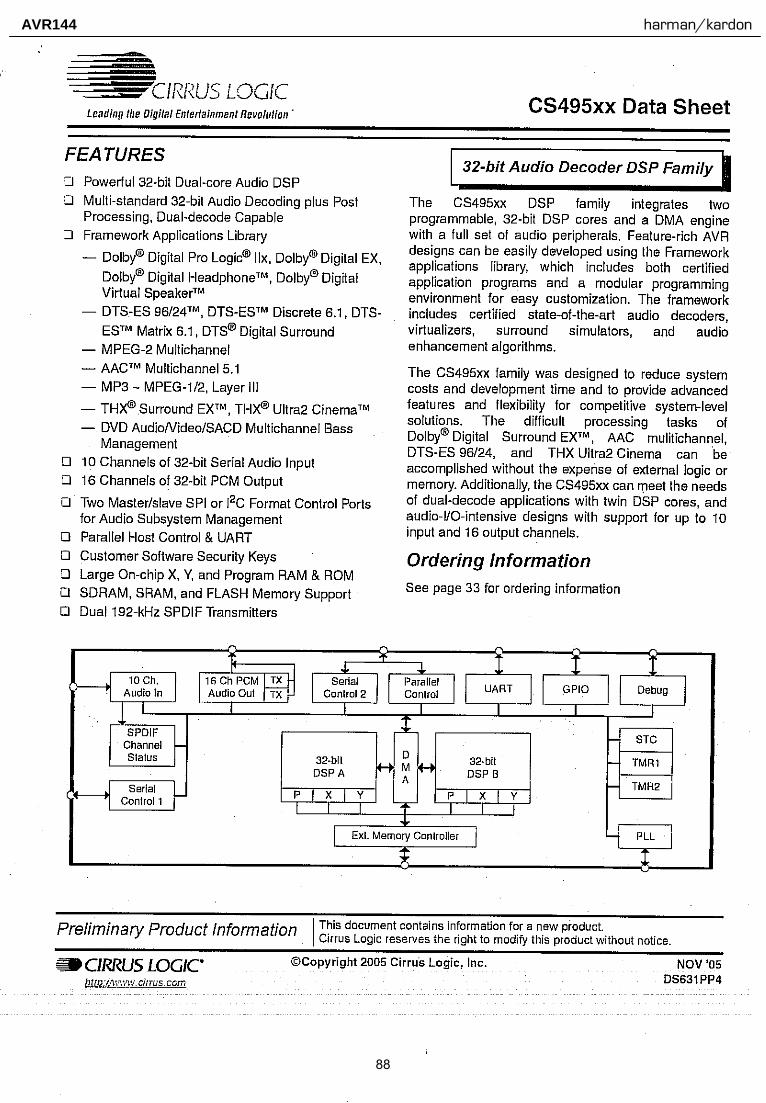
88
AVR144 harman/kardon

89
AVR144 harman/kardon
90
AVR144 harman/kardon
91
AVR144 harman/kardon

92
AVR144 harman/kardon
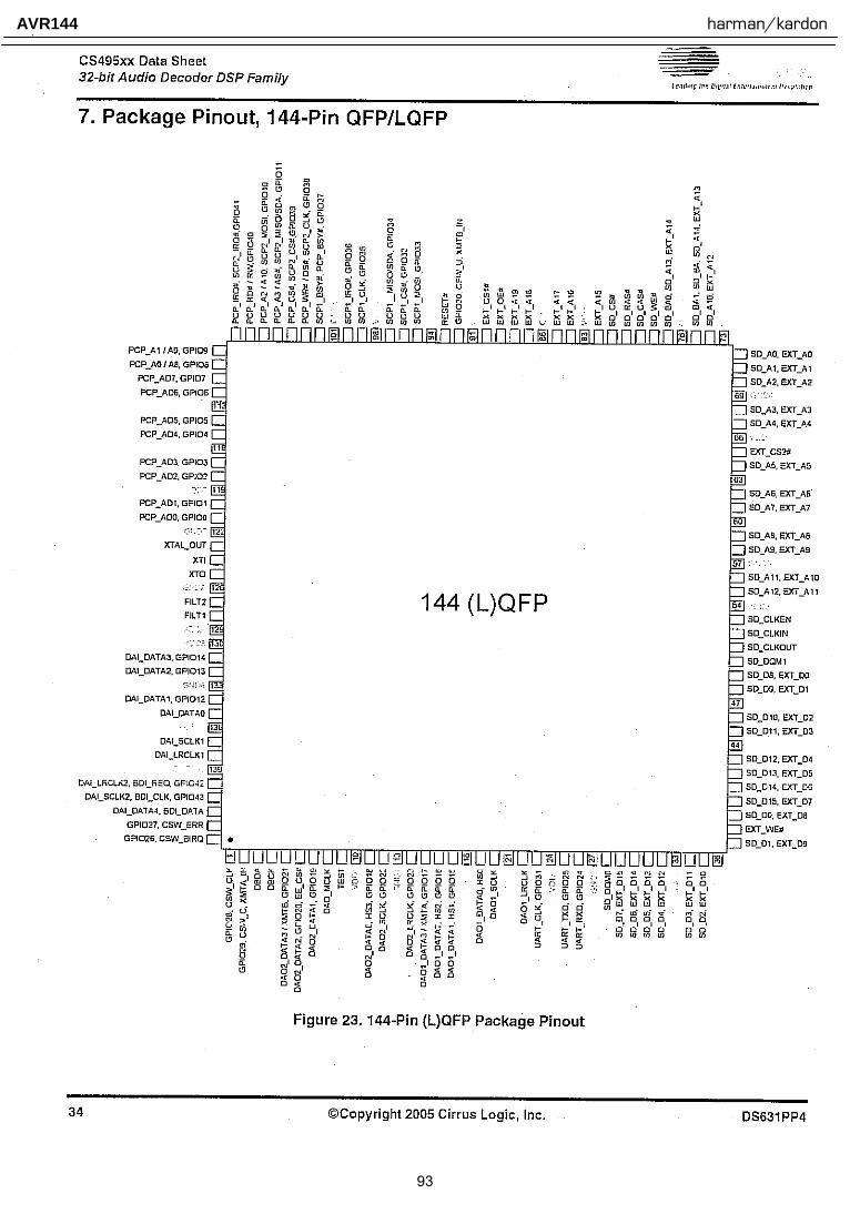
93
AVR144 harman/kardon
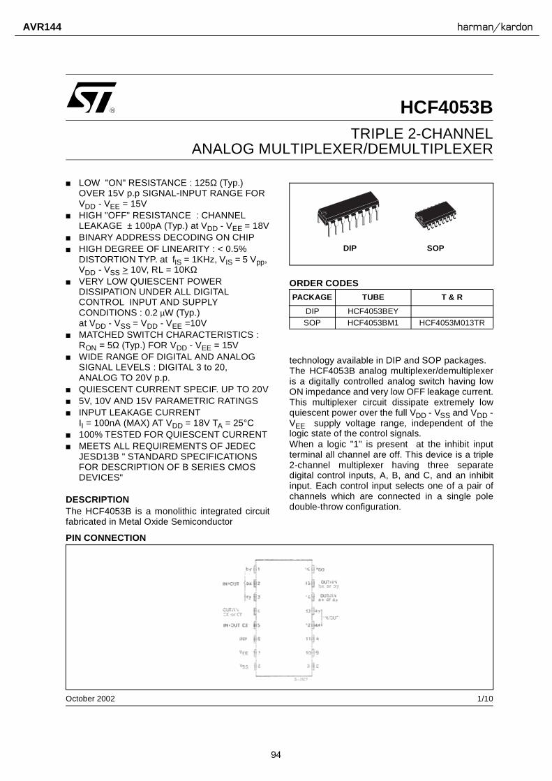
1/10October 2002
LOW "ON" RESISTANCE : 125Ω (Typ.)OVER 15V p.p SIGNAL-INPUT RANGE FORVDD - VEE = 15V
HIGH "OFF" RESISTANCE : CHANNELLEAKAGE ± 100pA (Typ.) at VDD - VEE = 18V
BINARY ADDRESS DECODING ON CHIP HIGH DEGREE OF LINEARITY : < 0.5%
DISTORTION TYP. at fIS = 1KHz, VIS = 5 Vpp,VDD - VSS > 10V, RL = 10KΩ
VERY LOW QUIESCENT POWERDISSIPATION UNDER ALL DIGITALCONTROL INPUT AND SUPPLYCONDITIONS : 0.2 µW (Typ.)at VDD - VSS = VDD - VEE =10V
MATCHED SWITCH CHARACTERISTICS :RON = 5Ω (Typ.) FOR VDD - VEE = 15V
WIDE RANGE OF DIGITAL AND ANALOGSIGNAL LEVELS : DIGITAL 3 to 20,ANALOG TO 20V p.p.
QUIESCENT CURRENT SPECIF. UP TO 20V 5V, 10V AND 15V PARAMETRIC RATINGS INPUT LEAKAGE CURRENT
II = 100nA (MAX) AT VDD = 18V TA = 25°C 100% TESTED FOR QUIESCENT CURRENT MEETS ALL REQUIREMENTS OF JEDEC
JESD13B " STANDARD SPECIFICATIONSFOR DESCRIPTION OF B SERIES CMOSDEVICES"
DESCRIPTIONThe HCF4053B is a monolithic integrated circuitfabricated in Metal Oxide Semiconductor
technology available in DIP and SOP packages.The HCF4053B analog multiplexer/demultiplexeris a digitally controlled analog switch having lowON impedance and very low OFF leakage current.This multiplexer circuit dissipate extremely lowquiescent power over the full VDD - VSS and VDD -VEE supply voltage range, independent of thelogic state of the control signals.When a logic "1" is present at the inhibit inputterminal all channel are off. This device is a triple2-channel multiplexer having three separatedigital control inputs, A, B, and C, and an inhibitinput. Each control input selects one of a pair ofchannels which are connected in a single poledouble-throw configuration.
HCF4053BTRIPLE 2-CHANNEL
ANALOG MULTIPLEXER/DEMULTIPLEXER
PIN CONNECTION
ORDER CODES
PACKAGE TUBE T & R
DIP HCF4053BEYSOP HCF4053BM1 HCF4053M013TR
DIP SOP
94
AVR144 harman/kardon

HCF4053B
2/10
INPUT EQUIVALENT CIRCUIT PIN DESCRIPTION
TRUTH TABLE
X : Don’t Care
FUNCTIONAL DIAGRAM
PIN No SYMBOL NAME AND FUNCTION
11, 10, 9 A, B, C Binary Control Inputs6 INH Inhibit Inputs
12, 13, 2, 1,5, 3
IN/OUTax,ay,bx,by,cx,cy Input/Output
14 OUT/IN ax or ay15 OUT/IN bx or by4 OUT/IN cx or cy
7 VEE Supply Voltage
8 VSS Negative Supply Voltage
16 VDD Positive Supply Voltage
INHIBIT C or B or A
0 0 ax or bx or cx0 1 ay or by or cy1 X NONE
95
AVR144 harman/kardon
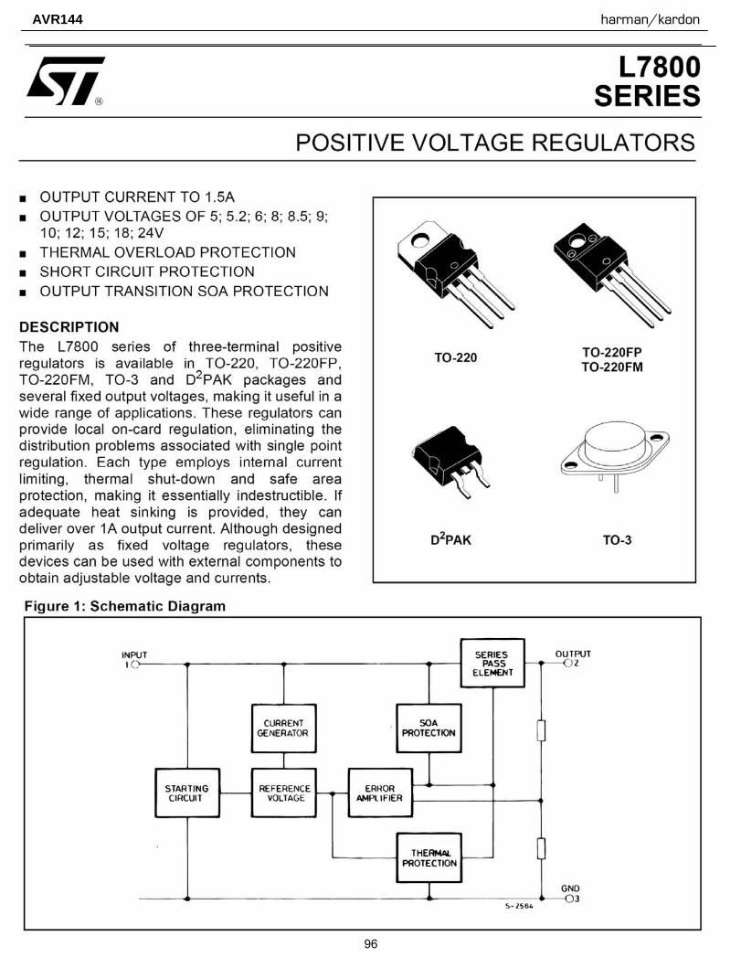
96
AVR144 harman/kardon
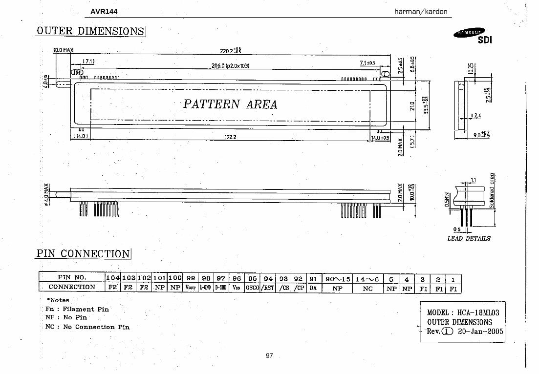
97
AVR144 harman/kardon

98
AVR144 harman/kardon
99
AVR144 harman/kardon
100
AVR144 harman/kardon
101
AVR144 harman/kardon

102
AVR144 harman/kardon
103
AVR144 harman/kardon

104
AVR144 harman/kardon
105
AVR144 harman/kardon

106
AVR144 harman/kardon

107
AVR144 harman/kardon
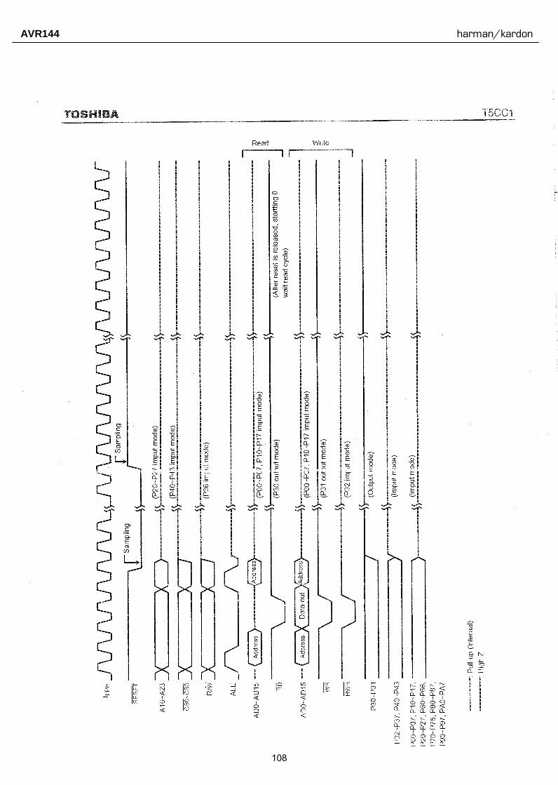
108
AVR144 harman/kardon

109
AVR144 harman/kardon
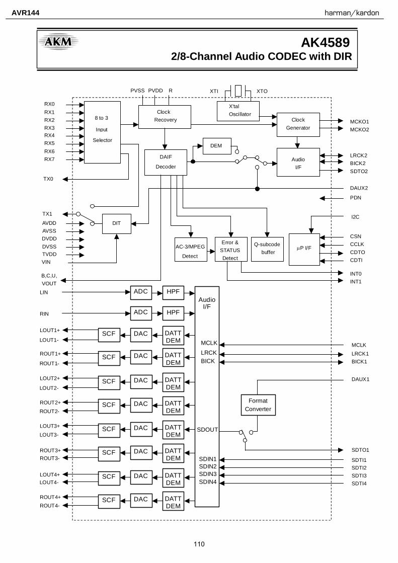
Input
Selector
ClockRecovery Clock
Generator
DAIF
Decoder
AC-3/MPEG
Detect
DEM
µP I/F
Audio I/F
X'talOscillator
PDN
INT0
LRCK2BICK2SDTO2
DAUX2
MCKO2
XTOXTIRPVDD PVSS
CDTICDTOCCLKCSNDVDD
DVSS TVDD
MCKO1
I2C
RX0 RX1 RX2 RX3 RX4 RX5 RX6 RX7
DIT
TX0
Error &
DetectSTATUS
INT1
Q-subcode buffer
TX1
B,C,U, VOUT
8 to 3
VIN
AudioI/F
SCF
SCF
SCF
SCF
SCF
SCF
LOUT1+
ROUT1+
LOUT2+
ROUT2+
LOUT3+
ROUT3+
DAC DATTDEM
ADC HPF
ADC HPFRIN
LIN
LRCK1BICK1
SDTI1 SDTI2 SDTI3
DAUX1
MCLKLRCKBICK
SDOUT
SDIN1SDIN2SDIN3
MCLK
SDTO1
Format Converter
SDTI4 SDIN4SCF
SCF
LOUT4+
ROUT4+
DAC DATTDEM
DAC DATTDEM
DAC DATTDEM
DAC DATTDEM
DAC DATTDEM
DAC DATTDEM
DAC DATTDEM
AVDD AVSS
LOUT1-
ROUT1-
LOUT2-
ROUT2-
LOUT3-
ROUT3-
LOUT4-
ROUT4-
2/8-Channel Audio CODEC with DIRAK4589
110
AVR144 harman/kardon

ASAHI KASEI [AK4589]
MS0339-J-00 2004/09 - 4 -
オーダリングガイド
AK4589VQ -10 ∼ +70°C 80pin LQFP(0.5mm pitch) AKD4589 評価ボード
ピン配置
(Top View)
CC
LK/S
CL
CD
TI/S
DA
CSN
DAU
X1SD
TI4
SDTI
3SD
TI2
SDTI
1XT
L1XT
L0PD
NM
ASTE
RD
ZF2
DZF
1LO
UT4
-LO
UT4
+R
OU
T4-
RO
UT4
+LO
UT3
-LO
UT3
+
21
22
23
24
25
26
27
28
29
30
31
32
33
34
35
36
37
38
39
40
60 59 58 57 56 55 54 53 52 51 50 49 48 47 46 45 44 43 42 41
80
79
78
77
76
75
74
73
72
71
70
69
68
67
66
65
64
63
62
61
1 2 3 4 5 6 7 8 9 10 11 12 13 14 15 16 17 18 19 20
INT1 BOUT TVDD DVDD DVSS
XTO XTI
TEST3 MCKO2 MCKO1
COUT UOUT VOUT
SDTO2 BICK2
LRCK2 SDTO1 BICK1
LRCK1 CDTO
TEST1 RX1 NC RX0 AVSS AVDD VREFH VCOM RIN LIN ROUT1+ ROUT1- LOUT1+ LOUT1- ROUT2+ ROUT2- LOUT2+ LOUT2- ROUT3+ ROUT3-
INT0
TX
1 TX
0 M
CLK
VI
N
DAU
X2
I2C
R
X7
CAD
1 R
X6
CAD
0 R
X5
TEST
2 R
X4
PVD
D
R
PVSS
R
X3
NC
R
X2
111
AVR144 harman/kardon
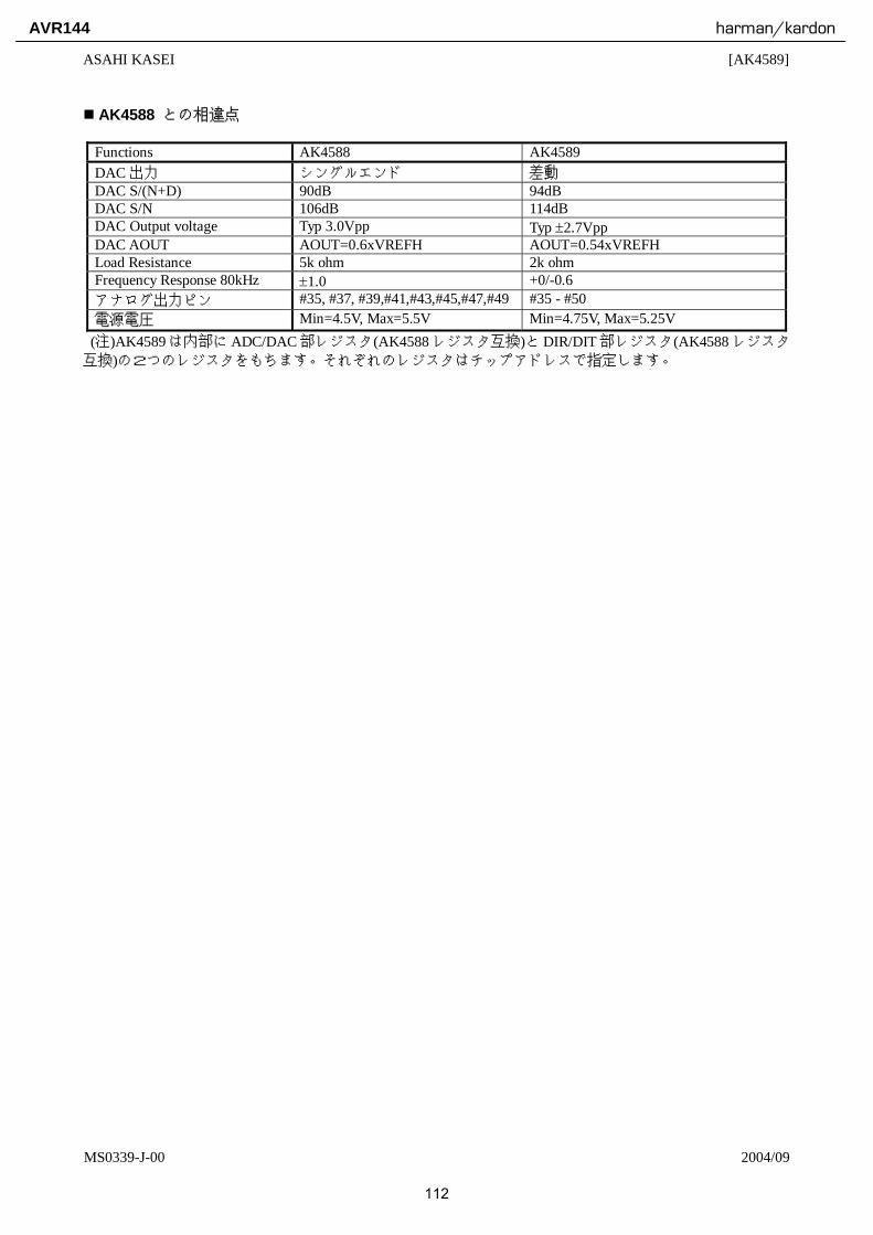
ASAHI KASEI [AK4589]
MS0339-J-00 2004/09 - 5 -
AK4588 との相違点
Functions AK4588 AK4589 DAC出力 シングルエンド 差動 DAC S/(N+D) 90dB 94dB DAC S/N 106dB 114dB DAC Output voltage Typ 3.0Vpp Typ ±2.7Vpp DAC AOUT AOUT=0.6xVREFH AOUT=0.54xVREFH Load Resistance 5k ohm 2k ohm Frequency Response 80kHz ±1.0 +0/-0.6 アナログ出力ピン #35, #37, #39,#41,#43,#45,#47,#49 #35 - #50 電源電圧 Min=4.5V, Max=5.5V Min=4.75V, Max=5.25V
(注)AK4589は内部にADC/DAC部レジスタ(AK4588レジスタ互換)とDIR/DIT部レジスタ(AK4588レジスタ互換)の2つのレジスタをもちます。それぞれのレジスタはチップアドレスで指定します。
112
AVR144 harman/kardon
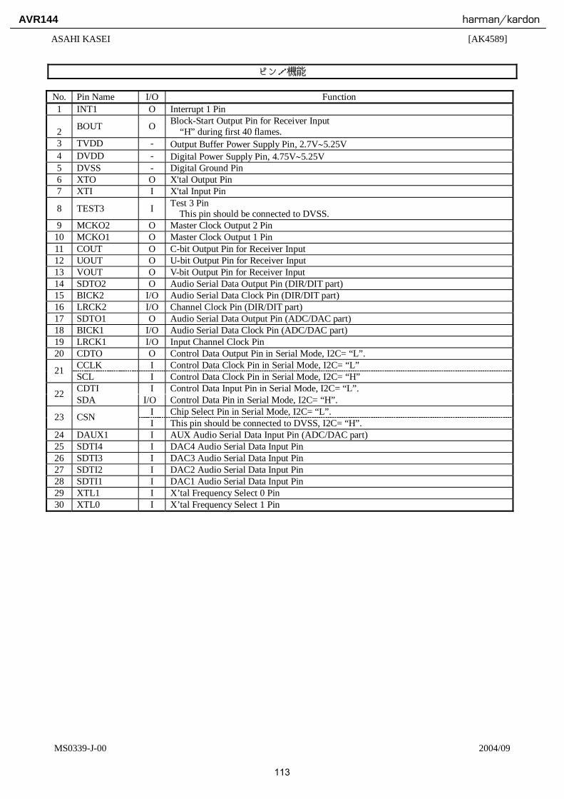
ASAHI KASEI [AK4589]
MS0339-J-00 2004/09 - 6 -
ピン/機能 No. Pin Name I/O Function 1 INT1 O Interrupt 1 Pin 2 BOUT O Block-Start Output Pin for Receiver Input
“H” during first 40 flames. 3 TVDD - Output Buffer Power Supply Pin, 2.7V∼5.25V 4 DVDD - Digital Power Supply Pin, 4.75V∼5.25V 5 DVSS - Digital Ground Pin 6 XTO O X'tal Output Pin 7 XTI I X'tal Input Pin
8 TEST3 I Test 3 Pin This pin should be connected to DVSS.
9 MCKO2 O Master Clock Output 2 Pin 10 MCKO1 O Master Clock Output 1 Pin 11 COUT O C-bit Output Pin for Receiver Input 12 UOUT O U-bit Output Pin for Receiver Input 13 VOUT O V-bit Output Pin for Receiver Input 14 SDTO2 O Audio Serial Data Output Pin (DIR/DIT part) 15 BICK2 I/O Audio Serial Data Clock Pin (DIR/DIT part) 16 LRCK2 I/O Channel Clock Pin (DIR/DIT part) 17 SDTO1 O Audio Serial Data Output Pin (ADC/DAC part) 18 BICK1 I/O Audio Serial Data Clock Pin (ADC/DAC part) 19 LRCK1 I/O Input Channel Clock Pin 20 CDTO O Control Data Output Pin in Serial Mode, I2C= “L”.
CCLK I Control Data Clock Pin in Serial Mode, I2C= “L” 21 SCL I Control Data Clock Pin in Serial Mode, I2C= “H” CDTI I Control Data Input Pin in Serial Mode, I2C= “L”. 22 SDA I/O Control Data Pin in Serial Mode, I2C= “H”.
I Chip Select Pin in Serial Mode, I2C= “L”. 23 CSN I This pin should be connected to DVSS, I2C= “H”. 24 DAUX1 I AUX Audio Serial Data Input Pin (ADC/DAC part) 25 SDTI4 I DAC4 Audio Serial Data Input Pin 26 SDTI3 I DAC3 Audio Serial Data Input Pin 27 SDTI2 I DAC2 Audio Serial Data Input Pin 28 SDTI1 I DAC1 Audio Serial Data Input Pin 29 XTL1 I X’tal Frequency Select 0 Pin 30 XTL0 I X’tal Frequency Select 1 Pin
113
AVR144 harman/kardon
ASAHI KASEI [AK4589]
MS0339-J-00 2004/09 - 7 -
No. Pin Name I/O Function
31 PDN I Power-Down Mode Pin
When “L”, the AK4589 is powered-down, all digital output pins go “L”, all registers are reset. When CAD1/0 pins are changed, the AK4589 should be reset by PDN pin.
32 MASTER I Master Mode Select Pin “H”: Master mode, “L”: Slave mode
DZF2 O
Zero Input Detect 2 Pin (Table 13) When the input data of the group 1 follow total 8192 LRCK cycles with “0” input data, this pin goes to “H”. And when RSTN bit is “0”, PWDAN bit is “0”, this pin goes to “H”. It always is in “L” when P/S pin is “H”. 33
OVF O Analog Input Overflow Detect Pin This pin goes to “H” if the analog input of Lch or Rch overflows.
34 DZF1 O
Zero Input Detect 1 Pin (Table 13) When the input data of the group 1 follow total 8192 LRCK cycles with “0” input data, this pin goes to “H”. And when RSTN bit is “0”, PWDAN bit is “0”, this pin goes to “H”. Output is selected by setting DZFE pin when P/S pin is “H”.
35 LOUT4- O DAC4 Lch Negative Analog Output Pin 36 LOUT4+ O DAC4 Lch Positive Analog Output Pin
470pF capacitor should be connected between LOUT4- and LOUT4+.
37 ROUT4- O DAC4 Rch Negative Analog Output Pin 38 ROUT4+ O DAC4 Rch Positive Analog Output Pin
470pF capacitor should be connected between ROUT4- and ROUT4+.
39 LOUT3- O DAC3 Lch Negative Analog Output Pin 40 LOUT3+ O DAC3 Lch Positive Analog Output Pin
470pF capacitor should be connected between LOUT3- and LOUT3+.
41 ROUT3- O DAC3 Rch Negative Analog Output Pin 42 ROUT3+ O DAC3 Rch Positive Analog Output Pin
470pF capacitor should be connected between ROUT3- and ROUT3+.
43 LOUT2- O DAC2 Lch Negative Analog Output Pin 44 LOUT2+ O DAC2 Lch Positive Analog Output Pin
470pF capacitor should be connected between LOUT2- and LOUT2+.
45 ROUT2- O DAC2 Rch Negative Analog Output Pin 46 ROUT2+ O DAC2 Rch Positive Analog Output Pin
470pF capacitor should be connected between ROUT2- and ROUT2+.
47 LOUT1- O DAC1 Lch Negative Analog Output Pin 48 LOUT1+ O DAC1 Lch Positive Analog Output Pin
470pF capacitor should be connected between LOUT1- and LOUT1+.
49 ROUT1- O DAC1 Rch Negative Analog Output Pin 50 ROUT1+ O DAC1 Rch Positive Analog Output Pin
470pF capacitor should be connected between ROUT1- and ROUT1+.
51 LIN I Lch Analog Input Pin 52 RIN I Rch Analog Input Pin
53 VCOM - Common Voltage Output Pin 2.2µF capacitor should be connected to AVSS externally.
54 VREFH - Positive Voltage Reference Input Pin, AVDD
114
AVR144 harman/kardon
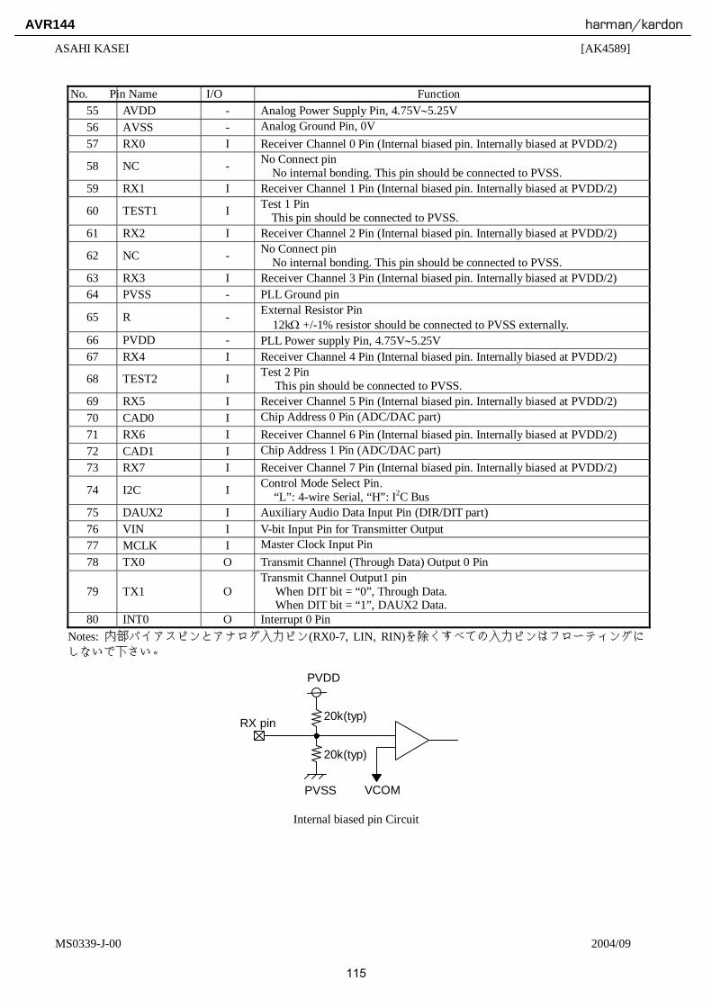
ASAHI KASEI [AK4589]
MS0339-J-00 2004/09 - 8 -
No. Pin Name I/O Function 55 AVDD - Analog Power Supply Pin, 4.75V∼5.25V 56 AVSS - Analog Ground Pin, 0V 57 RX0 I Receiver Channel 0 Pin (Internal biased pin. Internally biased at PVDD/2)
58 NC - No Connect pin No internal bonding. This pin should be connected to PVSS.
59 RX1 I Receiver Channel 1 Pin (Internal biased pin. Internally biased at PVDD/2)
60 TEST1 I Test 1 Pin This pin should be connected to PVSS.
61 RX2 I Receiver Channel 2 Pin (Internal biased pin. Internally biased at PVDD/2)
62 NC - No Connect pin No internal bonding. This pin should be connected to PVSS.
63 RX3 I Receiver Channel 3 Pin (Internal biased pin. Internally biased at PVDD/2) 64 PVSS - PLL Ground pin
65 R - External Resistor Pin 12kΩ +/-1% resistor should be connected to PVSS externally.
66 PVDD - PLL Power supply Pin, 4.75V∼5.25V 67 RX4 I Receiver Channel 4 Pin (Internal biased pin. Internally biased at PVDD/2)
68 TEST2 I Test 2 Pin This pin should be connected to PVSS.
69 RX5 I Receiver Channel 5 Pin (Internal biased pin. Internally biased at PVDD/2) 70 CAD0 I Chip Address 0 Pin (ADC/DAC part) 71 RX6 I Receiver Channel 6 Pin (Internal biased pin. Internally biased at PVDD/2) 72 CAD1 I Chip Address 1 Pin (ADC/DAC part) 73 RX7 I Receiver Channel 7 Pin (Internal biased pin. Internally biased at PVDD/2)
74 I2C I Control Mode Select Pin. “L”: 4-wire Serial, “H”: I2C Bus
75 DAUX2 I Auxiliary Audio Data Input Pin (DIR/DIT part) 76 VIN I V-bit Input Pin for Transmitter Output 77 MCLK I Master Clock Input Pin 78 TX0 O Transmit Channel (Through Data) Output 0 Pin
79 TX1 O Transmit Channel Output1 pin
When DIT bit = “0”, Through Data. When DIT bit = “1”, DAUX2 Data.
80 INT0 O Interrupt 0 Pin Notes: 内部バイアスピンとアナログ入力ピン(RX0-7, LIN, RIN)を除くすべての入力ピンはフローティングにしないで下さい。
VCOM
PVDD
PVSS
RX pin 20k(typ)
20k(typ)
Internal biased pin Circuit
115
AVR144 harman/kardon

ASAHI KASEI [AK4589]
MS0339-J-00 2004/09 - 9 -
使用しないピンの処理について 使用しない入出力ピンは下記の設定を行い、適切に処理して下さい。 Classification Pin Name Setting Analog RX0-7, LOUT1-4, ROUT1-4, LIN, RIN These pins should be open.
INT0-1, BOUT, XTO, MCKO1-2, COUT, UOUT, VOUT, SDTO1-2, CDTO, DZF1-2, TX1-0
These pins should be open.
CSN, DAUX1-2, SDTI1-4, XTL0-1 These pins should be connected to DVSS. Digital
TEST1-3 These pins should be connected to PVSS.
116
AVR144 harman/kardon

117
AVR144 harman/kardon
1/42September 2004
M29W800DTM29W800DB
8 Mbit (1Mb x8 or 512Kb x16, Boot Block)3V Supply Flash Memory
FEATURES SUMMARY SUPPLY VOLTAGE
– VCC = 2.7V to 3.6V for Program, Erase and Read
ACCESS TIMES: 45, 70, 90ns PROGRAMMING TIME
– 10µs per Byte/Word typical 19 MEMORY BLOCKS
– 1 Boot Block (Top or Bottom Location)– 2 Parameter and 16 Main Blocks
PROGRAM/ERASE CONTROLLER– Embedded Byte/Word Program
algorithms ERASE SUSPEND and RESUME MODES
– Read and Program another Block duringErase Suspend
UNLOCK BYPASS PROGRAM COMMAND– Faster Production/Batch Programming
TEMPORARY BLOCK UNPROTECTION MODE
COMMON FLASH INTERFACE– 64 bit Security Code
LOW POWER CONSUMPTION– Standby and Automatic Standby
100,000 PROGRAM/ERASE CYCLES per BLOCK
ELECTRONIC SIGNATURE– Manufacturer Code: 0020h– Top Device Code M29W800DT: 22D7h– Bottom Device Code M29W800DB:
225Bh
Figure 1. Packages
TSOP48 (N)12 x 20mm
TFBGA48 (ZA)6 x 9 mm
FBGA
SO44 (M)
TFBGA48 (ZE)6 x 8mm
FBGA
118
AVR144 harman/kardon
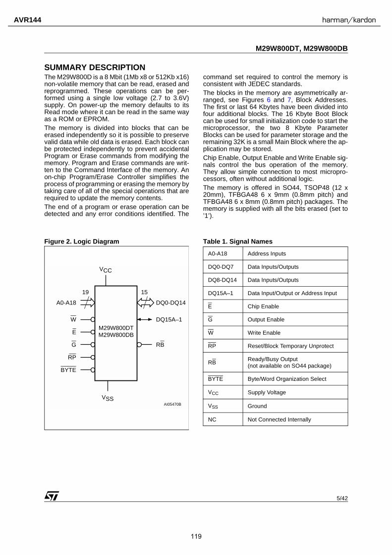
5/42
M29W800DT, M29W800DB
SUMMARY DESCRIPTIONThe M29W800D is a 8 Mbit (1Mb x8 or 512Kb x16)non-volatile memory that can be read, erased andreprogrammed. These operations can be per-formed using a single low voltage (2.7 to 3.6V)supply. On power-up the memory defaults to itsRead mode where it can be read in the same wayas a ROM or EPROM.The memory is divided into blocks that can beerased independently so it is possible to preservevalid data while old data is erased. Each block canbe protected independently to prevent accidentalProgram or Erase commands from modifying thememory. Program and Erase commands are writ-ten to the Command Interface of the memory. Anon-chip Program/Erase Controller simplifies theprocess of programming or erasing the memory bytaking care of all of the special operations that arerequired to update the memory contents.The end of a program or erase operation can bedetected and any error conditions identified. The
command set required to control the memory isconsistent with JEDEC standards.The blocks in the memory are asymmetrically ar-ranged, see Figures 6 and 7, Block Addresses.The first or last 64 Kbytes have been divided intofour additional blocks. The 16 Kbyte Boot Blockcan be used for small initialization code to start themicroprocessor, the two 8 Kbyte ParameterBlocks can be used for parameter storage and theremaining 32K is a small Main Block where the ap-plication may be stored.Chip Enable, Output Enable and Write Enable sig-nals control the bus operation of the memory.They allow simple connection to most micropro-cessors, often without additional logic.The memory is offered in SO44, TSOP48 (12 x20mm), TFBGA48 6 x 9mm (0.8mm pitch) andTFBGA48 6 x 8mm (0.8mm pitch) packages. Thememory is supplied with all the bits erased (set to’1’).
Figure 2. Logic Diagram Table 1. Signal Names
AI05470B
19
A0-A18
W
DQ0-DQ14
VCC
M29W800DTM29W800DBE
VSS
15
G
RP
DQ15A–1
RB
BYTE
A0-A18 Address Inputs
DQ0-DQ7 Data Inputs/Outputs
DQ8-DQ14 Data Inputs/Outputs
DQ15A–1 Data Input/Output or Address Input
E Chip Enable
G Output Enable
W Write Enable
RP Reset/Block Temporary Unprotect
RBReady/Busy Output(not available on SO44 package)
BYTE Byte/Word Organization Select
VCC Supply Voltage
VSS Ground
NC Not Connected Internally
119
AVR144 harman/kardon
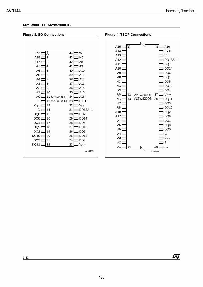
M29W800DT, M29W800DB
6/42
Figure 3. SO Connections Figure 4. TSOP Connections
GDQ0DQ8
A3
A0E
VSS
A2A1
A13
VSS
A14A15
DQ7
A12
A16BYTE
DQ15A–1
DQ5DQ2
DQ3VCCDQ11DQ4
DQ14
A9
NCRP
A4
W
A7
AI05462b
M29W800DTM29W800DB
8
234567
910111213141516
3231302928272625242322
20191817DQ1
DQ9
A6A5
DQ6DQ13
44
39383736353433
A11A10
DQ1021
DQ12
40
431
4241
A17 A8A18
DQ3
DQ9DQ2
A6DQ0
W
A3
RB
DQ6A8A9
DQ13
A17
A10 DQ14
A2
DQ12
DQ10
DQ15A–1
VCC
DQ4
DQ5
A7
DQ7
NCNC
AI05461
M29W800DTM29W800DB
12
1
13
24 25
3637
48
DQ8
NCNC
A1
A18
A4A5
DQ1
DQ11
G
A12A13
A16
A11
BYTEA15A14
VSS
EA0
RP
VSS
120
AVR144 harman/kardon

M29W800DT, M29W800DB
8/42
Figure 6. Block Addresses (x8)
Note: Also see APPENDIX A., Tables 21 and 22 for a full listing of the Block Addresses.
AI05463
16 KByteFFFFFh
FC000h
64 KByte
1FFFFh
10000h
64 KByte0FFFFh
00000h
M29W800DT Top Boot Block Addresses (x8)
32 KByteF7FFFh
F0000h
64 KByteE0000h
EFFFFh
Total of 1564 KByte Blocks
16 KByte
FFFFFh
F0000h64 KByte
64 KByte
03FFFh
00000h
M29W800DB Bottom Boot Block Addresses (x8)
32 KByte
EFFFFh
1FFFFh64 KByte
E0000h
10000h
Total of 1564 KByte Blocks
0FFFFh
08000h
8 KByte
8 KByte
FBFFFh
FA000hF9FFFh
F8000h
8 KByte
8 KByte
07FFFh
06000h05FFFh
04000h
121
AVR144 harman/kardon
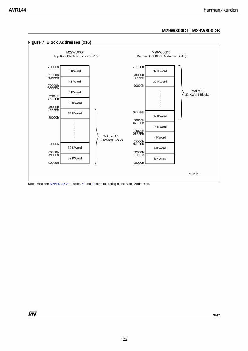
9/42
M29W800DT, M29W800DB
Figure 7. Block Addresses (x16)
Note: Also see APPENDIX A., Tables 21 and 22 for a full listing of the Block Addresses.
AI05464
8 KWord7FFFFh
7E000h
32 KWord
0FFFFh
08000h
32 KWord07FFFh
00000h
M29W800DT Top Boot Block Addresses (x16)
16 KWord7BFFFh
78000h
32 KWord70000h
77FFFh
Total of 1532 KWord Blocks
8 KWord
7FFFFh
78000h32 KWord
32 KWord
01FFFh
00000h
M29W800DB Bottom Boot Block Addresses (x16)
16 KWord
77FFFh
0FFFFh32 KWord
70000h
08000h
Total of 1532 KWord Blocks
07FFFh
04000h
4 KWord
4 KWord
7DFFFh
7D000h7CFFFh
7C000h
4 KWord
4 KWord
03FFFh
03000h02FFFh
02000h
122
AVR144 harman/kardon

M29W800DT, M29W800DB
10/42
SIGNAL DESCRIPTIONSSee Figure 2., Logic Diagram, and Table1., Signal Names, for a brief overview of the sig-nals connected to this device.Address Inputs (A0-A18). The Address Inputsselect the cells in the memory array to access dur-ing Bus Read operations. During Bus Write opera-tions they control the commands sent to theCommand Interface of the internal state machine.Data Inputs/Outputs (DQ0-DQ7). The Data In-puts/Outputs output the data stored at the selectedaddress during a Bus Read operation. During BusWrite operations they represent the commandssent to the Command Interface of the internal statemachine.Data Inputs/Outputs (DQ8-DQ14). The Data In-puts/Outputs output the data stored at the selectedaddress during a Bus Read operation when BYTEis High, VIH. When BYTE is Low, VIL, these pinsare not used and are high impedance. During BusWrite operations the Command Register does notuse these bits. When reading the Status Registerthese bits should be ignored.Data Input/Output or Address Input (DQ15A-1). When BYTE is High, VIH, this pin behaves asa Data Input/Output pin (as DQ8-DQ14). WhenBYTE is Low, VIL, this pin behaves as an addresspin; DQ15A–1 Low will select the LSB of the Wordon the other addresses, DQ15A–1 High will selectthe MSB. Throughout the text consider referencesto the Data Input/Output to include this pin whenBYTE is High and references to the Address In-puts to include this pin when BYTE is Low exceptwhen stated explicitly otherwise.Chip Enable (E). The Chip Enable, E, activatesthe memory, allowing Bus Read and Bus Write op-erations to be performed. When Chip Enable isHigh, VIH, all other pins are ignored.Output Enable (G). The Output Enable, G, con-trols the Bus Read operation of the memory.Write Enable (W). The Write Enable, W, controlsthe Bus Write operation of the memory’s Com-mand Interface.Reset/Block Temporary Unprotect (RP). TheReset/Block Temporary Unprotect pin can beused to apply a Hardware Reset to the memory orto temporarily unprotect all Blocks that have beenprotected.A Hardware Reset is achieved by holding Reset/Block Temporary Unprotect Low, VIL, for at leasttPLPX. After Reset/Block Temporary Unprotectgoes High, VIH, the memory will be ready for BusRead and Bus Write operations after tPHEL or
tRHEL, whichever occurs last. See the Ready/BusyOutput section, Table 15. and Figure 15., Reset/Block Temporary Unprotect AC Waveforms, formore details.Holding RP at VID will temporarily unprotect theprotected Blocks in the memory. Program andErase operations on all blocks will be possible.The transition from VIH to VID must be slower thantPHPHH.Ready/Busy Output (RB). The Ready/Busy pinis an open-drain output that can be used to identifywhen the device is performing a Program or Eraseoperation. During Program or Erase operationsReady/Busy is Low, VOL. Ready/Busy is high-im-pedance during Read mode, Auto Select modeand Erase Suspend mode. After a Hardware Reset, Bus Read and Bus Writeoperations cannot begin until Ready/Busy be-comes high-impedance. See Table 15., Reset/Block Temporary Unprotect AC Characteristicsand Figure 15., Reset/Block Temporary UnprotectAC Waveforms. The use of an open-drain output allows the Ready/Busy pins from several memories to be connectedto a single pull-up resistor. A Low will then indicatethat one, or more, of the memories is busy.Byte/Word Organization Select (BYTE). TheByte/Word Organization Select pin is used toswitch between the 8-bit and 16-bit Bus modes ofthe memory. When Byte/Word Organization Se-lect is Low, VIL, the memory is in 8-bit mode, whenit is High, VIH, the memory is in 16-bit mode.VCC Supply Voltage. The VCC Supply Voltagesupplies the power for all operations (Read, Pro-gram, Erase etc.).The Command Interface is disabled when the VCCSupply Voltage is less than the Lockout Voltage,VLKO. This prevents Bus Write operations from ac-cidentally damaging the data during power up,power down and power surges. If the Program/Erase Controller is programming or erasing duringthis time then the operation aborts and the memo-ry contents being altered will be invalid.A 0.1µF capacitor should be connected betweenthe VCC Supply Voltage pin and the VSS Groundpin to decouple the current surges from the powersupply. The PCB track widths must be sufficient tocarry the currents required during program anderase operations, ICC3.VSS Ground. The VSS Ground is the reference forall voltage measurements.
123
AVR144 harman/kardon

11/42
M29W800DT, M29W800DB
BUS OPERATIONSThere are five standard bus operations that controlthe device. These are Bus Read, Bus Write, Out-put Disable, Standby and Automatic Standby. SeeTables 2 and 3, Bus Operations, for a summary.Typically glitches of less than 5ns on Chip Enableor Write Enable are ignored by the memory and donot affect bus operations.Bus Read. Bus Read operations read from thememory cells, or specific registers in the Com-mand Interface. A valid Bus Read operation in-volves setting the desired address on the AddressInputs, applying a Low signal, VIL, to Chip Enableand Output Enable and keeping Write EnableHigh, VIH. The Data Inputs/Outputs will output thevalue, see Figure 12., Read Mode AC Waveforms,and Table 12., Read AC Characteristics for detailsof when the output becomes valid.Bus Write. Bus Write operations write to theCommand Interface. A valid Bus Write operationbegins by setting the desired address on the Ad-dress Inputs. The Address Inputs are latched bythe Command Interface on the falling edge of ChipEnable or Write Enable, whichever occurs last.The Data Inputs/Outputs are latched by the Com-mand Interface on the rising edge of Chip Enableor Write Enable, whichever occurs first. Output En-able must remain High, VIH, during the whole BusWrite operation. See Figures 13 and 14, Write ACWaveforms, and Tables 13 and 14, Write ACCharacteristics, for details of the timing require-ments.Output Disable. The Data Inputs/Outputs are inthe high impedance state when Output Enable isHigh, VIH.Standby. When Chip Enable is High, VIH, thememory enters Standby mode and the Data In-puts/Outputs pins are placed in the high-imped-
ance state. To reduce the Supply Current to theStandby Supply Current, ICC2, Chip Enable shouldbe held within VCC ± 0.2V. For the Standby currentlevel see Table 11., DC Characteristics.During program or erase operations the memorywill continue to use the Program/Erase SupplyCurrent, ICC3, for Program or Erase operations un-til the operation completes.Automatic Standby. If CMOS levels (VCC ± 0.2V)are used to drive the bus and the bus is inactive for150ns or more the memory enters AutomaticStandby where the internal Supply Current is re-duced to the Standby Supply Current, ICC2. TheData Inputs/Outputs will still output data if a BusRead operation is in progress.Special Bus Operations. Additional bus opera-tions can be performed to read the Electronic Sig-nature and also to apply and remove BlockProtection. These bus operations are intended foruse by programming equipment and are not usu-ally used in applications. They require VID to beapplied to some pins.Electronic Signature. The memory has twocodes, the manufacturer code and the devicecode, that can be read to identify the memory.These codes can be read by applying the signalslisted in Tables 2 and 3, Bus Operations.Block Protection and Blocks Unprotection.Each block can be separately protected againstaccidental Program or Erase. Protected blockscan be unprotected to allow data to be changed. There are two methods available for protectingand unprotecting the blocks, one for use on pro-gramming equipment and the other for in-systemuse. Block Protect and Chip Unprotect operationsare described in APPENDIX C.
Table 2. Bus Operations, BYTE = VIL
Note: X = VIL or VIH.
Operation E G W Address InputsDQ15A–1, A0-A18
Data Inputs/Outputs
DQ14-DQ8 DQ7-DQ0
Bus Read VIL VIL VIH Cell Address Hi-Z Data Output
Bus Write VIL VIH VIL Command Address Hi-Z Data Input
Output Disable X VIH VIH X Hi-Z Hi-Z
Standby VIH X X X Hi-Z Hi-Z
Read Manufacturer Code
VIL VIL VIHA0 = VIL, A1 = VIL, A9 = VID, Others VIL or VIH
Hi-Z 20h
Read Device Code VIL VIL VIHA0 = VIH, A1 = VIL, A9 = VID, Others VIL or VIH
Hi-ZD7h (M29W800DT)5Bh (M29W800DB)
124
AVR144 harman/kardon
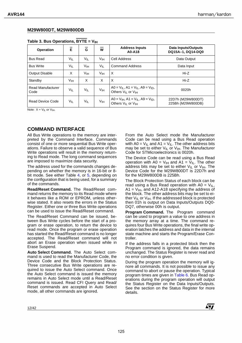
M29W800DT, M29W800DB
12/42
Table 3. Bus Operations, BYTE = VIH
Note: X = VIL or VIH.
COMMAND INTERFACEAll Bus Write operations to the memory are inter-preted by the Command Interface. Commandsconsist of one or more sequential Bus Write oper-ations. Failure to observe a valid sequence of BusWrite operations will result in the memory return-ing to Read mode. The long command sequencesare imposed to maximize data security.The address used for the commands changes de-pending on whether the memory is in 16-bit or 8-bit mode. See either Table 4, or 5, depending onthe configuration that is being used, for a summaryof the commands.Read/Reset Command. The Read/Reset com-mand returns the memory to its Read mode whereit behaves like a ROM or EPROM, unless other-wise stated. It also resets the errors in the StatusRegister. Either one or three Bus Write operationscan be used to issue the Read/Reset command.The Read/Reset Command can be issued, be-tween Bus Write cycles before the start of a pro-gram or erase operation, to return the device toread mode. Once the program or erase operationhas started the Read/Reset command is no longeraccepted. The Read/Reset command will notabort an Erase operation when issued while inErase Suspend.Auto Select Command. The Auto Select com-mand is used to read the Manufacturer Code, theDevice Code and the Block Protection Status.Three consecutive Bus Write operations are re-quired to issue the Auto Select command. Oncethe Auto Select command is issued the memoryremains in Auto Select mode until a Read/Resetcommand is issued. Read CFI Query and Read/Reset commands are accepted in Auto Selectmode, all other commands are ignored.
From the Auto Select mode the ManufacturerCode can be read using a Bus Read operationwith A0 = VIL and A1 = VIL. The other address bitsmay be set to either VIL or VIH. The ManufacturerCode for STMicroelectronics is 0020h.The Device Code can be read using a Bus Readoperation with A0 = VIH and A1 = VIL. The otheraddress bits may be set to either VIL or VIH. TheDevice Code for the M29W800DT is 22D7h andfor the M29W800DB is 225Bh.The Block Protection Status of each block can beread using a Bus Read operation with A0 = VIL,A1 = VIH, and A12-A18 specifying the address ofthe block. The other address bits may be set to ei-ther VIL or VIH. If the addressed block is protectedthen 01h is output on Data Inputs/Outputs DQ0-DQ7, otherwise 00h is output.Program Command. The Program commandcan be used to program a value to one address inthe memory array at a time. The command re-quires four Bus Write operations, the final write op-eration latches the address and data in the internalstate machine and starts the Program/Erase Con-troller. If the address falls in a protected block then theProgram command is ignored, the data remainsunchanged. The Status Register is never read andno error condition is given.During the program operation the memory will ig-nore all commands. It is not possible to issue anycommand to abort or pause the operation. Typicalprogram times are given in Table 6. Bus Read op-erations during the program operation will outputthe Status Register on the Data Inputs/Outputs.See the section on the Status Register for moredetails.
Operation E G W Address InputsA0-A18
Data Inputs/OutputsDQ15A–1, DQ14-DQ0
Bus Read VIL VIL VIH Cell Address Data Output
Bus Write VIL VIH VIL Command Address Data Input
Output Disable X VIH VIH X Hi-Z
Standby VIH X X X Hi-Z
Read Manufacturer Code
VIL VIL VIHA0 = VIL, A1 = VIL, A9 = VID, Others VIL or VIH
0020h
Read Device Code VIL VIL VIHA0 = VIH, A1 = VIL, A9 = VID, Others VIL or VIH
22D7h (M29W800DT)225Bh (M29W800DB)
125
AVR144 harman/kardon
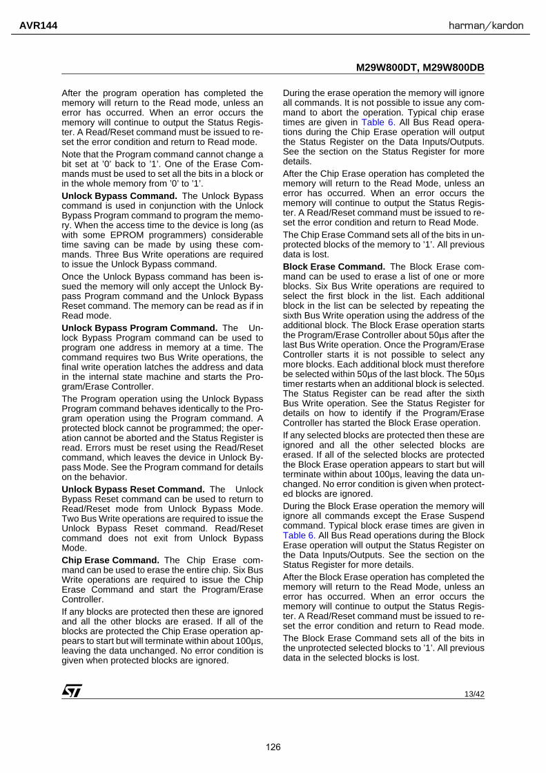
13/42
M29W800DT, M29W800DB
After the program operation has completed thememory will return to the Read mode, unless anerror has occurred. When an error occurs thememory will continue to output the Status Regis-ter. A Read/Reset command must be issued to re-set the error condition and return to Read mode.Note that the Program command cannot change abit set at ’0’ back to ’1’. One of the Erase Com-mands must be used to set all the bits in a block orin the whole memory from ’0’ to ’1’.Unlock Bypass Command. The Unlock Bypasscommand is used in conjunction with the UnlockBypass Program command to program the memo-ry. When the access time to the device is long (aswith some EPROM programmers) considerabletime saving can be made by using these com-mands. Three Bus Write operations are requiredto issue the Unlock Bypass command.Once the Unlock Bypass command has been is-sued the memory will only accept the Unlock By-pass Program command and the Unlock BypassReset command. The memory can be read as if inRead mode.Unlock Bypass Program Command. The Un-lock Bypass Program command can be used toprogram one address in memory at a time. Thecommand requires two Bus Write operations, thefinal write operation latches the address and datain the internal state machine and starts the Pro-gram/Erase Controller.The Program operation using the Unlock BypassProgram command behaves identically to the Pro-gram operation using the Program command. Aprotected block cannot be programmed; the oper-ation cannot be aborted and the Status Register isread. Errors must be reset using the Read/Resetcommand, which leaves the device in Unlock By-pass Mode. See the Program command for detailson the behavior.Unlock Bypass Reset Command. The UnlockBypass Reset command can be used to return toRead/Reset mode from Unlock Bypass Mode.Two Bus Write operations are required to issue theUnlock Bypass Reset command. Read/Resetcommand does not exit from Unlock BypassMode.Chip Erase Command. The Chip Erase com-mand can be used to erase the entire chip. Six BusWrite operations are required to issue the ChipErase Command and start the Program/EraseController.If any blocks are protected then these are ignoredand all the other blocks are erased. If all of theblocks are protected the Chip Erase operation ap-pears to start but will terminate within about 100µs,leaving the data unchanged. No error condition isgiven when protected blocks are ignored.
During the erase operation the memory will ignoreall commands. It is not possible to issue any com-mand to abort the operation. Typical chip erasetimes are given in Table 6. All Bus Read opera-tions during the Chip Erase operation will outputthe Status Register on the Data Inputs/Outputs.See the section on the Status Register for moredetails.After the Chip Erase operation has completed thememory will return to the Read Mode, unless anerror has occurred. When an error occurs thememory will continue to output the Status Regis-ter. A Read/Reset command must be issued to re-set the error condition and return to Read Mode.The Chip Erase Command sets all of the bits in un-protected blocks of the memory to ’1’. All previousdata is lost.Block Erase Command. The Block Erase com-mand can be used to erase a list of one or moreblocks. Six Bus Write operations are required toselect the first block in the list. Each additionalblock in the list can be selected by repeating thesixth Bus Write operation using the address of theadditional block. The Block Erase operation startsthe Program/Erase Controller about 50µs after thelast Bus Write operation. Once the Program/EraseController starts it is not possible to select anymore blocks. Each additional block must thereforebe selected within 50µs of the last block. The 50µstimer restarts when an additional block is selected.The Status Register can be read after the sixthBus Write operation. See the Status Register fordetails on how to identify if the Program/EraseController has started the Block Erase operation. If any selected blocks are protected then these areignored and all the other selected blocks areerased. If all of the selected blocks are protectedthe Block Erase operation appears to start but willterminate within about 100µs, leaving the data un-changed. No error condition is given when protect-ed blocks are ignored.During the Block Erase operation the memory willignore all commands except the Erase Suspendcommand. Typical block erase times are given inTable 6. All Bus Read operations during the BlockErase operation will output the Status Register onthe Data Inputs/Outputs. See the section on theStatus Register for more details.After the Block Erase operation has completed thememory will return to the Read Mode, unless anerror has occurred. When an error occurs thememory will continue to output the Status Regis-ter. A Read/Reset command must be issued to re-set the error condition and return to Read mode.The Block Erase Command sets all of the bits inthe unprotected selected blocks to ’1’. All previousdata in the selected blocks is lost.
126
AVR144 harman/kardon
M29W800DT, M29W800DB
14/42
Erase Suspend Command. The Erase SuspendCommand may be used to temporarily suspend aBlock Erase operation and return the memory toRead mode. The command requires one BusWrite operation. The Program/Erase Controller will suspend withinthe Erase Suspend Latency Time (refer to Table 6.for value) of the Erase Suspend Command beingissued. Once the Program/Erase Controller hasstopped the memory will be set to Read mode andthe Erase will be suspended. If the Erase Suspendcommand is issued during the period when thememory is waiting for an additional block (beforethe Program/Erase Controller starts) then theErase is suspended immediately and will start im-mediately when the Erase Resume Command isissued. It is not possible to select any furtherblocks to erase after the Erase Resume.During Erase Suspend it is possible to Read andProgram cells in blocks that are not being erased;both Read and Program operations behave asnormal on these blocks. If any attempt is made toprogram in a protected block or in the suspendedblock then the Program command is ignored andthe data remains unchanged. The Status Registeris not read and no error condition is given. Read-ing from blocks that are being erased will outputthe Status Register. It is also possible to issue the Auto Select, ReadCFI Query and Unlock Bypass commands duringan Erase Suspend. The Read/Reset commandmust be issued to return the device to Read Array
mode before the Resume command will be ac-cepted.Erase Resume Command. The Erase Resumecommand must be used to restart the Program/Erase Controller from Erase Suspend. An erasecan be suspended and resumed more than once.Read CFI Query Command. The Read CFIQuery Command is used to read data from theCommon Flash Interface (CFI) Memory Area. Thiscommand is valid when the device is in the ReadArray mode, or when the device is in Auto Selectmode. One Bus Write cycle is required to issue the ReadCFI Query Command. Once the command is is-sued subsequent Bus Read operations read fromthe Common Flash Interface Memory Area.The Read/Reset command must be issued to re-turn the device to the previous mode (the Read Ar-ray mode or Auto Select mode). A second Read/Reset command would be needed if the device isto be put in the Read Array mode from Auto Selectmode.See APPENDIX B., Tables 23, 24, 25, 26, 27 and28 for details on the information contained in theCommon Flash Interface (CFI) memory area.Block Protect and Chip Unprotect Commands.Each block can be separately protected againstaccidental Program or Erase. The whole chip canbe unprotected to allow the data inside the blocksto be changed. Block Protect and Chip Unprotect operations aredescribed in APPENDIX C.
127
AVR144 harman/kardon

MITSUMI Video Switch · 75Ω driver · Y/C mix MM1501
Video Switch · 75Ω driver · Y/C mixMonolithic IC MM1501 Series
OutlineThis IC extends the series of ICs for video/audio signal switching, with a 2-input 1-output single video switch,video signal/chroma signal 75Ω driver, and Y/C mixing circuit in one small package (SOT-26).
Features(1) Low power consumption achieved.(2) Low power supply voltage realized.(3) Frequency bandwidth without 75Ω driver: 10MHz with 75Ω driver: 7MHz(4) Cross talk 70dB When 4.43MHz(5) With SAG measures pin (75Ω driver and Y/C mix driver)
Applications(1) TV(2) VTR(3) Video camera(4) Digital still camera(5) Other visual equipment
Line-up
Functions Model Name Input Output Clamp 6dB amp 75Ω driver SAG measures pin Power supply voltage
MM1501 4.5~13.0VMM1502 4.5~13.0VMM1503 4.5~13.0V
SwitchMM1504
2 14.5~13.0V
MM1505 4.5~13.0VMM1506 4.5~13.0VMM1507 4.5~13.0VMM1508 4.5~13.0V
DriverMM1509
1 14.5~13.0V
MM1510 4.5~13.0V
Y/C mixMM1511
1 1/ 4.5~13.0V
MM1512 / 4.5~13.0V
PackageSOT-26A (with 75Ω driver)SOT-26B (without 75Ω driver)
128
AVR144 harman/kardon

MITSUMI Video Switch · 75Ω driver · Y/C mix MM1501
Block Diagram
MM1501 MM1502
MM1503 MM1504
MM1505 MM1506
129
AVR144 harman/kardon
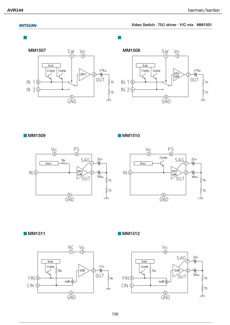
MITSUMI Video Switch · 75Ω driver · Y/C mix MM1501
MM1507 MM1508
MM1509 MM1510
MM1511 MM1512
130
AVR144 harman/kardon

131
AVR144 harman/kardon
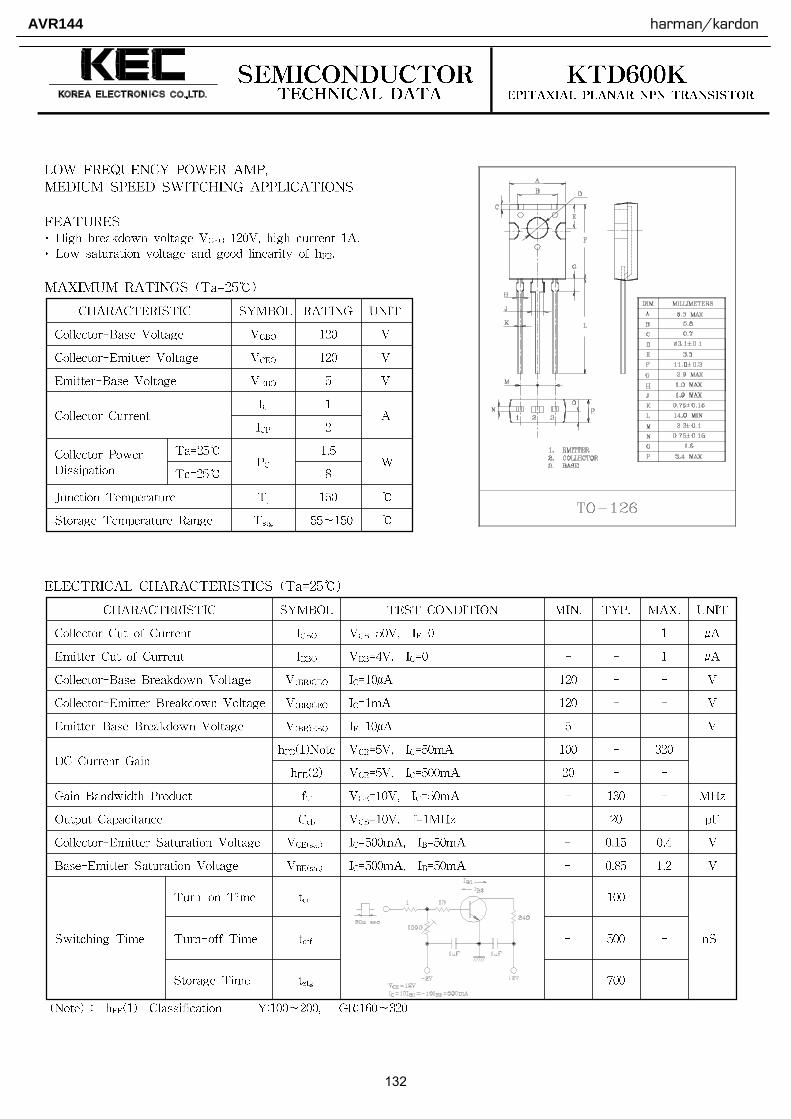
132
AVR144 harman/kardon
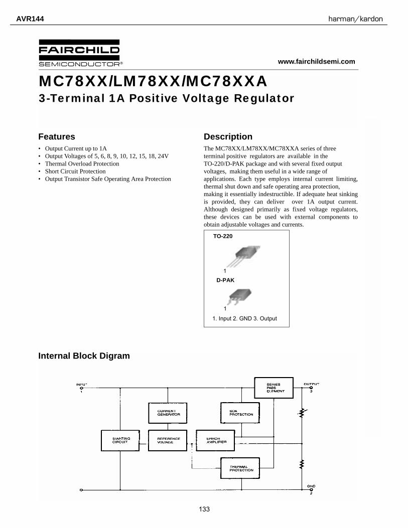
www.fairchildsemi.com
Features• Output Current up to 1A • Output Voltages of 5, 6, 8, 9, 10, 12, 15, 18, 24V • Thermal Overload Protection • Short Circuit Protection• Output Transistor Safe Operating Area Protection
DescriptionThe MC78XX/LM78XX/MC78XXA series of three terminal positive regulators are available in the TO-220/D-PAK package and with several fixed output voltages, making them useful in a wide range of applications. Each type employs internal current limiting,thermal shut down and safe operating area protection, making it essentially indestructible. If adequate heat sinkingis provided, they can deliver over 1A output current.Although designed primarily as fixed voltage regulators,these devices can be used with external components toobtain adjustable voltages and currents.
TO-220
D-PAK
1. Input 2. GND 3. Output
1
1
Internal Block Digram
MC78XX/LM78XX/MC78XXA3-Terminal 1A Positive Voltage Regulator
133
AVR144 harman/kardon

134
AVR144 harman/kardon
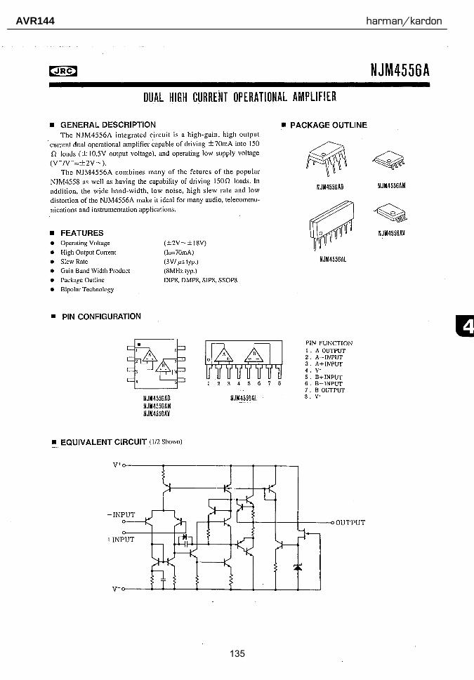
135
AVR144 harman/kardon

136
AVR144 harman/kardon
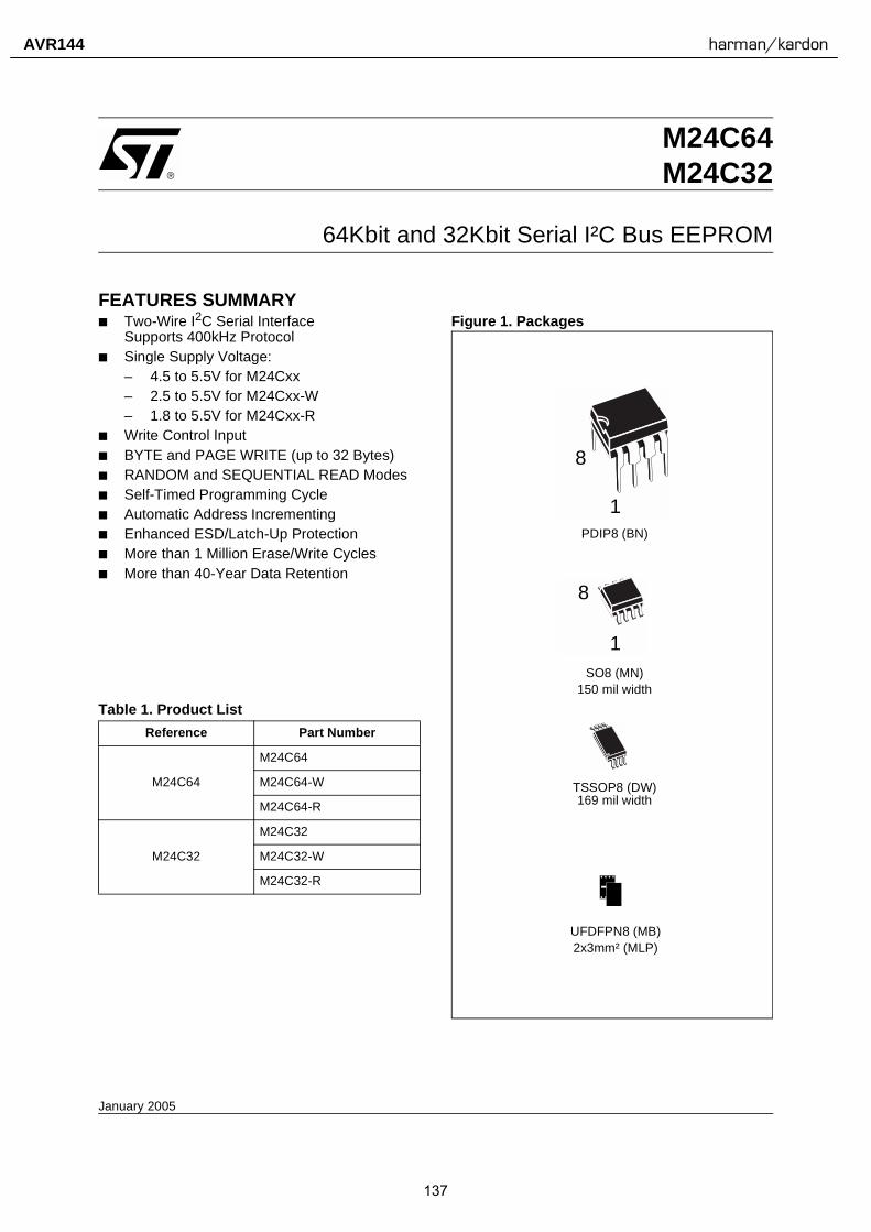
January 2005
M24C64M24C32
64Kbit and 32Kbit Serial I²C Bus EEPROM
FEATURES SUMMARY Two-Wire I2C Serial Interface
Supports 400kHz Protocol Single Supply Voltage:
– 4.5 to 5.5V for M24Cxx– 2.5 to 5.5V for M24Cxx-W– 1.8 to 5.5V for M24Cxx-R
Write Control Input BYTE and PAGE WRITE (up to 32 Bytes) RANDOM and SEQUENTIAL READ Modes Self-Timed Programming Cycle Automatic Address Incrementing Enhanced ESD/Latch-Up Protection More than 1 Million Erase/Write Cycles More than 40-Year Data Retention
Table 1. Product List
Figure 1. Packages
Reference Part Number
M24C64
M24C64
M24C64-W
M24C64-R
M24C32
M24C32
M24C32-W
M24C32-R
PDIP8 (BN)
8
1
SO8 (MN)150 mil width
8
1
TSSOP8 (DW)169 mil width
UFDFPN8 (MB)2x3mm² (MLP)
137
AVR144 harman/kardon
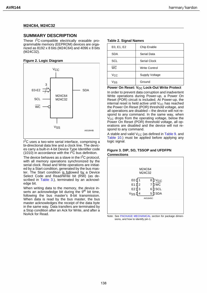
M24C64, M24C32
SUMMARY DESCRIPTIONThese I2C-compatible electrically erasable pro-grammable memory (EEPROM) devices are orga-nized as 8192 x 8 bits (M24C64) and 4096 x 8 bits(M24C32).
Figure 2. Logic Diagram
I2C uses a two-wire serial interface, comprising abi-directional data line and a clock line. The devic-es carry a built-in 4-bit Device Type Identifier code(1010) in accordance with the I2C bus definition.The device behaves as a slave in the I2C protocol,with all memory operations synchronized by theserial clock. Read and Write operations are initiat-ed by a Start condition, generated by the bus mas-ter. The Start condition is followed by a DeviceSelect Code and Read/Write bit (RW) (as de-scribed in Table 3.), terminated by an acknowl-edge bit.When writing data to the memory, the device in-serts an acknowledge bit during the 9th bit time,following the bus master’s 8-bit transmission.When data is read by the bus master, the busmaster acknowledges the receipt of the data bytein the same way. Data transfers are terminated bya Stop condition after an Ack for Write, and after aNoAck for Read.
Table 2. Signal Names
Power On Reset: VCC Lock-Out Write ProtectIn order to prevent data corruption and inadvertentWrite operations during Power-up, a Power OnReset (POR) circuit is included. At Power-up, theinternal reset is held active until VCC has reachedthe Power On Reset (POR) threshold voltage, andall operations are disabled – the device will not re-spond to any command. In the same way, whenVCC drops from the operating voltage, below thePower On Reset (POR) threshold voltage, all op-erations are disabled and the device will not re-spond to any command.A stable and valid VCC (as defined in Table 9. andTable 10.) must be applied before applying anylogic signal.
Figure 3. DIP, SO, TSSOP and UFDFPN Connections
Note: See PACKAGE MECHANICAL section for package dimen-sions, and how to identify pin-1.
AI01844B
3
E0-E2 SDA
VCC
M24C64M24C32
WC
SCL
VSS
E0, E1, E2 Chip Enable
SDA Serial Data
SCL Serial Clock
WC Write Control
VCC Supply Voltage
VSS Ground
SDAVSS
SCLWCE1
E0 VCC
E2
AI01845C
M24C64M24C32
1234
8765
138
AVR144 harman/kardon
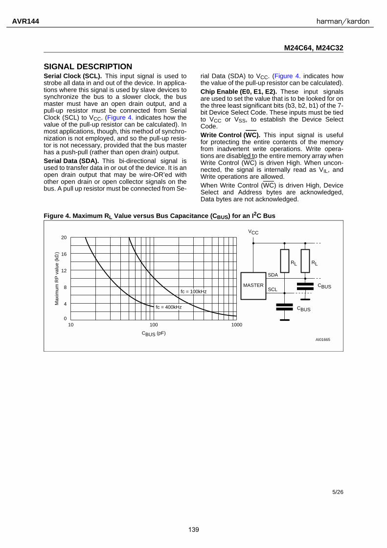
5/26
M24C64, M24C32
SIGNAL DESCRIPTIONSerial Clock (SCL). This input signal is used tostrobe all data in and out of the device. In applica-tions where this signal is used by slave devices tosynchronize the bus to a slower clock, the busmaster must have an open drain output, and apull-up resistor must be connected from SerialClock (SCL) to VCC. (Figure 4. indicates how thevalue of the pull-up resistor can be calculated). Inmost applications, though, this method of synchro-nization is not employed, and so the pull-up resis-tor is not necessary, provided that the bus masterhas a push-pull (rather than open drain) output.Serial Data (SDA). This bi-directional signal isused to transfer data in or out of the device. It is anopen drain output that may be wire-OR’ed withother open drain or open collector signals on thebus. A pull up resistor must be connected from Se-
rial Data (SDA) to VCC. (Figure 4. indicates howthe value of the pull-up resistor can be calculated).Chip Enable (E0, E1, E2). These input signalsare used to set the value that is to be looked for onthe three least significant bits (b3, b2, b1) of the 7-bit Device Select Code. These inputs must be tiedto VCC or VSS, to establish the Device SelectCode.Write Control (WC). This input signal is usefulfor protecting the entire contents of the memoryfrom inadvertent write operations. Write opera-tions are disabled to the entire memory array whenWrite Control (WC) is driven High. When uncon-nected, the signal is internally read as VIL, andWrite operations are allowed.When Write Control (WC) is driven High, DeviceSelect and Address bytes are acknowledged,Data bytes are not acknowledged.
Figure 4. Maximum RL Value versus Bus Capacitance (CBUS) for an I2C Bus
AI01665
VCC
CBUS
SDA
RL
MASTER
RL
SCLCBUS
1000
4
8
12
16
20
CBUS (pF)
Max
imum
RP
val
ue (
kΩ)
10 1000
fc = 400kHz
fc = 100kHz
139
AVR144 harman/kardon

7/26
M24C64, M24C32
MEMORY ORGANIZATIONThe memory is organized as shown in Figure 6..
Figure 6. Block Diagram
AI06899
WC
E1
E0Control Logic
High VoltageGenerator
I/O Shift Register
Address Registerand Counter
DataRegister
1 Page
X Decoder
Y D
ecod
erSCL
SDA
E2
140
AVR144 harman/kardon
M24C64, M24C32
DEVICE OPERATION The device supports the I2C protocol. This is sum-marized in Figure 5.. Any device that sends dataon to the bus is defined to be a transmitter, andany device that reads the data to be a receiver.The device that controls the data transfer is knownas the bus master, and the other as the slave de-vice. A data transfer can only be initiated by thebus master, which will also provide the serial clockfor synchronization. The M24Cxx device is alwaysa slave in all communication.Start ConditionStart is identified by a falling edge of Serial Data(SDA) while Serial Clock (SCL) is stable in theHigh state. A Start condition must precede anydata transfer command. The device continuouslymonitors (except during a Write cycle) Serial Data(SDA) and Serial Clock (SCL) for a Start condition,and will not respond unless one is given.Stop ConditionStop is identified by a rising edge of Serial Data(SDA) while Serial Clock (SCL) is stable and driv-en High. A Stop condition terminates communica-tion between the device and the bus master. ARead command that is followed by NoAck can befollowed by a Stop condition to force the deviceinto the Stand-by mode. A Stop condition at theend of a Write command triggers the internal Writecycle.Acknowledge Bit (ACK)The acknowledge bit is used to indicate a success-ful byte transfer. The bus transmitter, whether it bebus master or slave device, releases Serial Data(SDA) after sending eight bits of data. During the9th clock pulse period, the receiver pulls Serial
Data (SDA) Low to acknowledge the receipt of theeight data bits.Data InputDuring data input, the device samples Serial Data(SDA) on the rising edge of Serial Clock (SCL).For correct device operation, Serial Data (SDA)must be stable during the rising edge of SerialClock (SCL), and the Serial Data (SDA) signalmust change only when Serial Clock (SCL) is driv-en Low.Memory AddressingTo start communication between the bus masterand the slave device, the bus master must initiatea Start condition. Following this, the bus mastersends the Device Select Code, shown in Table 3.(on Serial Data (SDA), most significant bit first).The Device Select Code consists of a 4-bit DeviceType Identifier, and a 3-bit Chip Enable “Address”(E2, E1, E0). To address the memory array, the 4-bit Device Type Identifier is 1010b.Up to eight memory devices can be connected ona single I2C bus. Each one is given a unique 3-bitcode on the Chip Enable (E0, E1, E2) inputs.When the Device Select Code is received, the de-vice only responds if the Chip Enable Address isthe same as the value on the Chip Enable (E0, E1,E2) inputs.The 8th bit is the Read/Write bit (RW). This bit isset to 1 for Read and 0 for Write operations.If a match occurs on the Device Select code, thecorresponding device gives an acknowledgmenton Serial Data (SDA) during the 9th bit time. If thedevice does not match the Device Select code, itdeselects itself from the bus, and goes into Stand-by mode.
Table 6. Operating Modes
Note: 1. X = VIH or VIL.
Mode RW bit WC 1 Bytes Initial Sequence
Current Address Read 1 X 1 START, Device Select, RW = 1
Random Address Read0 X
1START, Device Select, RW = 0, Address
1 X reSTART, Device Select, RW = 1
Sequential Read 1 X ≥ 1 Similar to Current or Random Address Read
Byte Write 0 VIL 1 START, Device Select, RW = 0
Page Write 0 VIL ≤ 32 START, Device Select, RW = 0
141
AVR144 harman/kardon
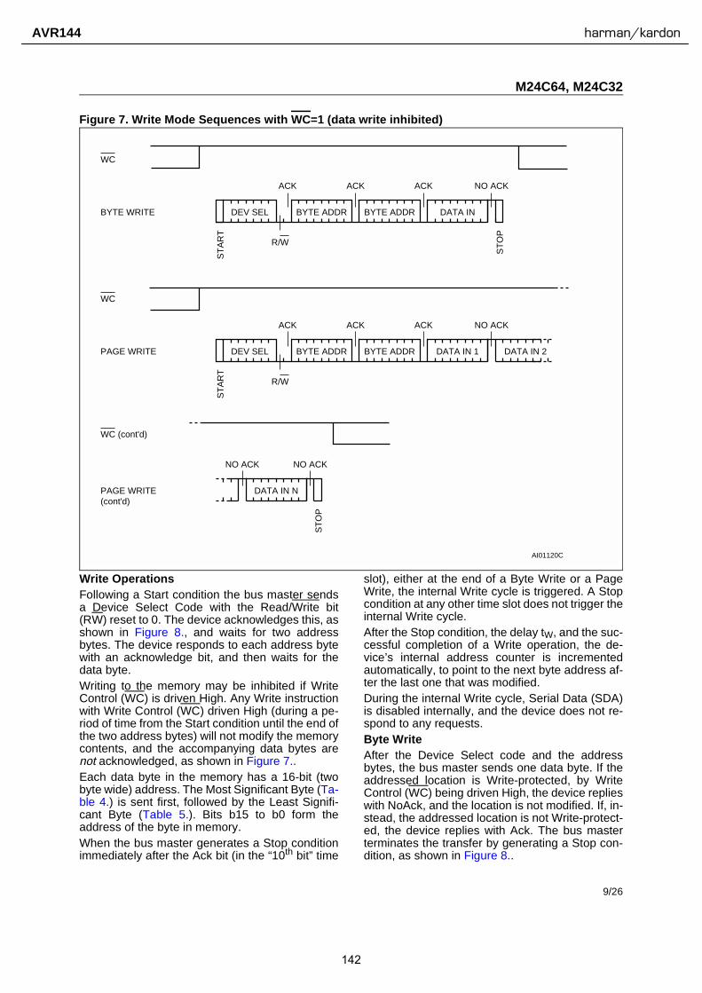
9/26
M24C64, M24C32
Figure 7. Write Mode Sequences with WC=1 (data write inhibited)
Write Operations Following a Start condition the bus master sendsa Device Select Code with the Read/Write bit(RW) reset to 0. The device acknowledges this, asshown in Figure 8., and waits for two addressbytes. The device responds to each address bytewith an acknowledge bit, and then waits for thedata byte.Writing to the memory may be inhibited if WriteControl (WC) is driven High. Any Write instructionwith Write Control (WC) driven High (during a pe-riod of time from the Start condition until the end ofthe two address bytes) will not modify the memorycontents, and the accompanying data bytes arenot acknowledged, as shown in Figure 7..Each data byte in the memory has a 16-bit (twobyte wide) address. The Most Significant Byte (Ta-ble 4.) is sent first, followed by the Least Signifi-cant Byte (Table 5.). Bits b15 to b0 form theaddress of the byte in memory.When the bus master generates a Stop conditionimmediately after the Ack bit (in the “10th bit” time
slot), either at the end of a Byte Write or a PageWrite, the internal Write cycle is triggered. A Stopcondition at any other time slot does not trigger theinternal Write cycle.After the Stop condition, the delay tW, and the suc-cessful completion of a Write operation, the de-vice’s internal address counter is incrementedautomatically, to point to the next byte address af-ter the last one that was modified.During the internal Write cycle, Serial Data (SDA)is disabled internally, and the device does not re-spond to any requests.Byte WriteAfter the Device Select code and the addressbytes, the bus master sends one data byte. If theaddressed location is Write-protected, by WriteControl (WC) being driven High, the device replieswith NoAck, and the location is not modified. If, in-stead, the addressed location is not Write-protect-ed, the device replies with Ack. The bus masterterminates the transfer by generating a Stop con-dition, as shown in Figure 8..
ST
OP
ST
AR
TBYTE WRITE DEV SEL BYTE ADDR BYTE ADDR DATA IN
WC
ST
AR
T
PAGE WRITE DEV SEL BYTE ADDR BYTE ADDR DATA IN 1
WC
DATA IN 2
AI01120C
PAGE WRITE(cont'd)
WC (cont'd)
ST
OP
DATA IN N
ACK ACK ACK NO ACK
R/W
ACK ACK ACK NO ACK
R/W
NO ACK NO ACK
142
AVR144 harman/kardon

M24C64, M24C32
Page WriteThe Page Write mode allows up to 32 bytes to bewritten in a single Write cycle, provided that theyare all located in the same ’row’ in the memory:that is, the most significant memory address bits(b12-b5 for M24C64, and b11-b5 for M24C32) arethe same. If more bytes are sent than will fit up tothe end of the row, a condition known as ‘roll-over’occurs. This should be avoided, as data starts tobecome overwritten in an implementation depen-dent way.
The bus master sends from 1 to 32 bytes of data,each of which is acknowledged by the device ifWrite Control (WC) is Low. If Write Control (WC) isHigh, the contents of the addressed memory loca-tion are not modified, and each data byte is fol-lowed by a NoAck. After each byte is transferred,the internal byte address counter (the 5 least sig-nificant address bits only) is incremented. Thetransfer is terminated by the bus master generat-ing a Stop condition.
Figure 8. Write Mode Sequences with WC=0 (data write enabled)
ST
OP
ST
AR
T
BYTE WRITE DEV SEL BYTE ADDR BYTE ADDR DATA IN
WC
ST
AR
T
PAGE WRITE DEV SEL BYTE ADDR BYTE ADDR DATA IN 1
WC
DATA IN 2
AI01106C
PAGE WRITE(cont'd)
WC (cont'd)
ST
OP
DATA IN N
ACK
R/W
ACK ACK ACK
ACK ACK ACK ACK
R/W
ACKACK
143
AVR144 harman/kardon

11/26
M24C64, M24C32
Figure 9. Write Cycle Polling Flowchart using ACK
Minimizing System Delays by Polling On ACKDuring the internal Write cycle, the device discon-nects itself from the bus, and writes a copy of thedata from its internal latches to the memory cells.The maximum Write time (tw) is shown in Table16. and Table 17., but the typical time is shorter.To make use of this, a polling sequence can beused by the bus master. The sequence, as shown in Figure 9., is:
– Initial condition: a Write cycle is in progress.– Step 1: the bus master issues a Start condition
followed by a Device Select Code (the first byte of the new instruction).
– Step 2: if the device is busy with the internal Write cycle, no Ack will be returned and the bus master goes back to Step 1. If the device has terminated the internal Write cycle, it responds with an Ack, indicating that the device is ready to receive the second part of the instruction (the first byte of this instruction having been sent during Step 1).
WRITE Cyclein Progress
AI01847C
NextOperation is
Addressing theMemory
START Condition
DEVICE SELECTwith RW = 0
ACKReturned
YES
NO
YESNO
ReSTART
STOP
DATA for theWRITE Operation
DEVICE SELECTwith RW = 1
Send Addressand Receive ACK
First byte of instructionwith RW = 0 alreadydecoded by the device
YESNO STARTCondition
Continue theWRITE Operation
Continue theRandom READ Operation
144
AVR144 harman/kardon

M24C64, M24C32
Figure 10. Read Mode Sequences
Note: 1. The seven most significant bits of the Device Select Code of a Random Read (in the 1st and 4th bytes) must be identical.
Read OperationsRead operations are performed independently ofthe state of the Write Control (WC) signal.After the successful completion of a Read opera-tion, the device’s internal address counter is incre-mented by one, to point to the next byte address.Random Address ReadA dummy Write is first performed to load the ad-dress into this address counter (as shown in Fig-ure 10.) but without sending a Stop condition.Then, the bus master sends another Start condi-tion, and repeats the Device Select Code, with theRead/Write bit (RW) set to 1. The device acknowl-edges this, and outputs the contents of the ad-
dressed byte. The bus master must notacknowledge the byte, and terminates the transferwith a Stop condition.Current Address ReadFor the Current Address Read operation, followinga Start condition, the bus master only sends a De-vice Select Code with the Read/Write bit (RW) setto 1. The device acknowledges this, and outputsthe byte addressed by the internal addresscounter. The counter is then incremented. The busmaster terminates the transfer with a Stop condi-tion, as shown in Figure 10., without acknowledg-ing the byte.
ST
AR
T
DEV SEL * BYTE ADDR BYTE ADDR
ST
AR
T
DEV SEL DATA OUT 1
AI01105C
DATA OUT N
ST
OP
ST
AR
T
CURRENTADDRESSREAD
DEV SEL DATA OUT
RANDOMADDRESSREAD
ST
OP
ST
AR
T
DEV SEL * DATA OUT
SEQUENTIALCURRENTREAD
ST
OP
DATA OUT N
ST
AR
T
DEV SEL * BYTE ADDR BYTE ADDRSEQUENTIALRANDOMREAD
ST
AR
T
DEV SEL * DATA OUT 1
ST
OP
ACK
R/W
NO ACK
ACK
R/W
ACK ACK ACK
R/W
ACK ACK ACK NO ACK
R/W
NO ACK
ACK ACK ACK
R/W
ACK ACK
R/W
ACK NO ACK
145
AVR144 harman/kardon
R×5VT
• TO-92
PIN CONFIGURATION• SOT-89 • SOT-23-5
PIN DESCRIPTION
• TO-92 • SOT-89 • SOT-23-5
Pin No. Symbol
1 OUT
2 VDD
3 GND
4 NC
5 NC
Pin No. Symbol
1 OUT
2 VDD
3 GND
Pin No. Symbol
1 OUT
2 VDD
3 GND
1 2 3
(mark side)
1 2 3
(mark side)
1 2 3
(mark side)
5 4
LOW VOLTAGE DETECTORR×5VT SERIES
146
AVR144 harman/kardon
• TO-92
PIN CONFIGURATION
• SOT-89 • SOT-23-5
PIN DESCRIPTION
• TO-92 • SOT-89 • SOT-23-5
Pin No Symbol
1 OUT
2 VDD
3 GND
4 NC
5 NC
Pin No Symbol
1 OUT
2 VDD
3 GND
Pin No Symbol
1 OUT
2 VDD
3 GND
1 2 3
(mark side)
1 2 3
(mark side)
1 2 3
(mark side)
5 4
R×5VL
VOLTAGE DETECTORR×5VL SERIES
147
AVR144 harman/kardon

1A LOWDROP OUT VOLTAGE REGULATOR (ADJUSTABLE & FIXED) LM1117
FEATURES
Output Current up to 1 A
Low Dropout Voltage ( 700mV at 1A Output Current )
Three Terminal Adjustable or Fixed 1.5V, 1.8V, 2.5V, 2.85V,
3.0V, 3.3V, 5.0V 2.85V Device for SCSI-II Active Terminator 0.04% Line Regulaion, 0.1% Load Regulation
Very Low Quiescent Current
Internal Current andTerminal Limit
Logic-Controlled Electronics Shutdown
Surface Mount Package SOT-223 & TO-263 (D2-Pack)
100% Thermal Limit Burn-In
APPLICATION
Active SCSI Terminators
Portable/Plan Top/Notebook Computers
High Efficiency Linear Regulators
SMPS Post Regulators ORDERING INFORMATION
Mother B/D Clock Supplies Package
Disk Drives
Battery Chargers
DESCRIPTION (X=Output Voltage=1.5V, 1.8V, 2.5V, 2.85V,
'3.0V, 3.3V, 5.0V, Adjustable=AD)
The LM1117 is a low power positive-voltage regulator designed to meet 1A output current and comply
with SCSI-II specifications with a fixed output voltage of 2.85V. This device is an excellent choice for use
in battery-powered applications, as active terminators for the SCSI bus, and portable computers.
The LM1117 features very low quiescent current and very low dropout voltage of 700mV at a full load and
lower as output current decreases. LM1117 is available as an adjustable or fixed 1.5V, 1.8V, 2.5V, 2.85V,
3.0V, 3.3V, and 5.0V output voltages.
The LM1117 is offered in a 3-pin surface mount package SOT-223 & TO-263. The output capacitor of
10 or larger is needed for output stability of LM1117 as required by most of the other regulator circuits.
ABSOLUTE MAXIMUM RATINGS
HTC
LM1117T
LM1117T-XX TO-263 (D2)
Device (Marking)
SOT-223 LM1117S
LM1117S-XX
MIN. UNIT
V
0
7
125
-65 150
Lead Temperature (Soldering, 5 Seconds) TSOL
1
CHARACTERISTIC
DC Input Voltage
Operating Junction Temperature Range
SYMBOL
VIN
TOPR
Storage Temperature Range TSTG
MAX.
260
1 2 3
SOT-223 PKG (FRONT VIEW)
PIN FUNCTION
1. Adj/Gnd
2. Vout
3. Vin
TO-263 (D2 PKG, FRONT VIEW)
PIN FUNCTION
1. Adj/Gnd
2. Vout
3. Vin
1 2 3
148
AVR144 harman/kardon
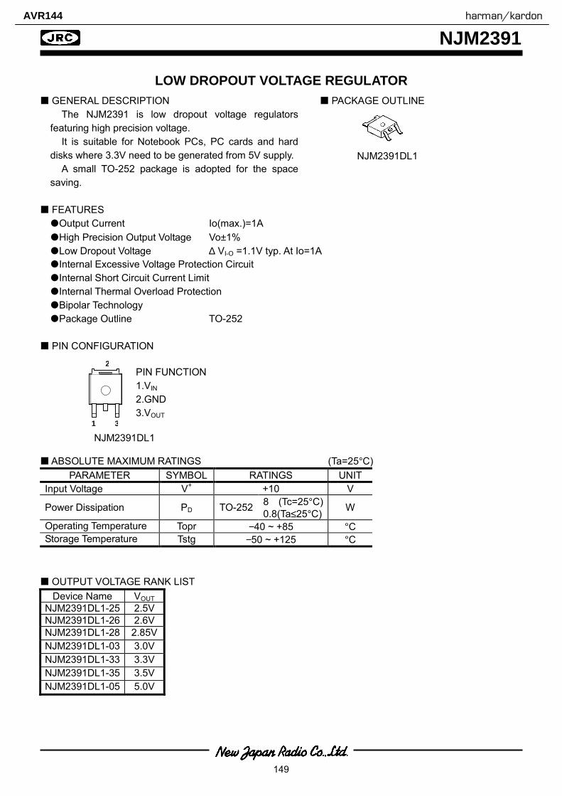
NJM2391
PIN FUNCTION 1.VIN 2.GND 3.VOUT
NJM2391DL1
LOW DROPOUT VOLTAGE REGULATOR GENERAL DESCRIPTION PACKAGE OUTLINE
The NJM2391 is low dropout voltage regulators featuring high precision voltage.
It is suitable for Notebook PCs, PC cards and hard disks where 3.3V need to be generated from 5V supply.
A small TO-252 package is adopted for the space saving.
FEATURES
Output Current Io(max.)=1A High Precision Output Voltage Vo±1% Low Dropout Voltage ∆ VI-O =1.1V typ. At Io=1A Internal Excessive Voltage Protection Circuit Internal Short Circuit Current Limit Internal Thermal Overload Protection Bipolar Technology Package Outline TO-252
PIN CONFIGURATION
ABSOLUTE MAXIMUM RATINGS (Ta=25°C) PARAMETER SYMBOL RATINGS UNIT
Input Voltage V+ +10 V
Power Dissipation PD TO-252 8 (Tc=25°C)0.8(Ta≤25°C) W
Operating Temperature Topr −40 ~ +85 °C Storage Temperature Tstg −50 ~ +125 °C
OUTPUT VOLTAGE RANK LIST Device Name VOUT
NJM2391DL1-25 2.5V NJM2391DL1-26 2.6V NJM2391DL1-28 2.85V NJM2391DL1-03 3.0V NJM2391DL1-33 3.3V NJM2391DL1-35 3.5V NJM2391DL1-05 5.0V
NJM2391DL1
31
2
149
AVR144 harman/kardon
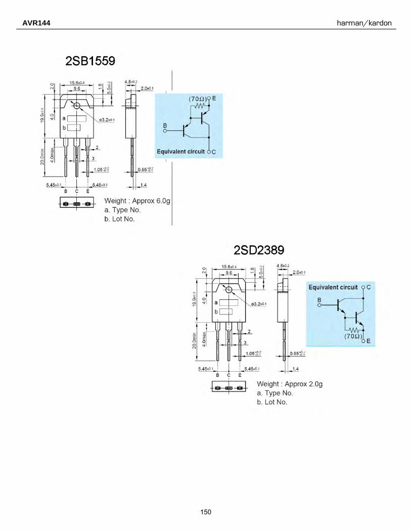
150
AVR144 harman/kardon

151
AVR144 harman/kardon
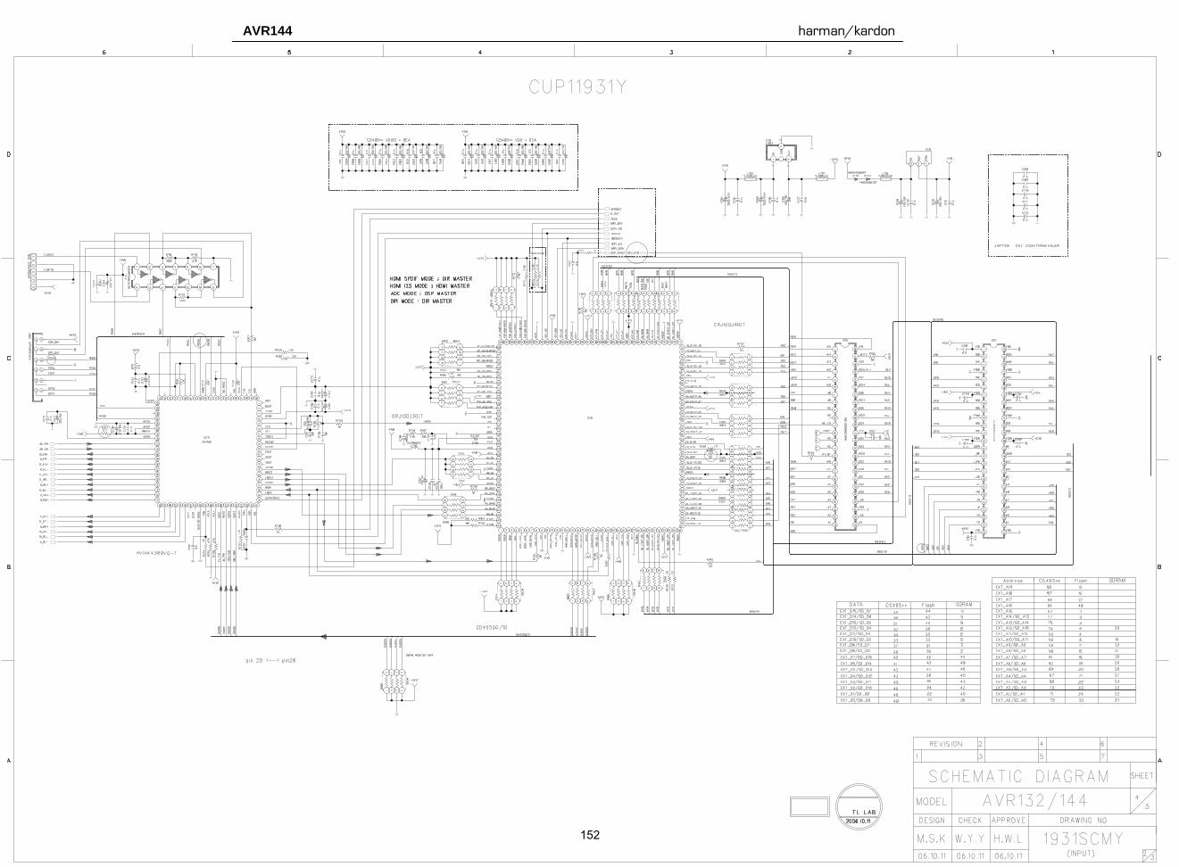
152
AVR144 harman/kardon

153
AVR144 harman/kardon
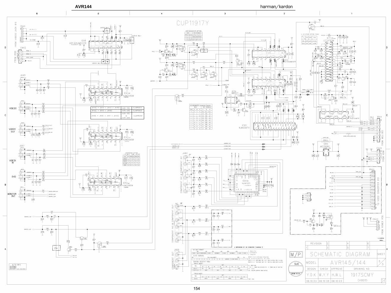
154
AVR144 harman/kardon
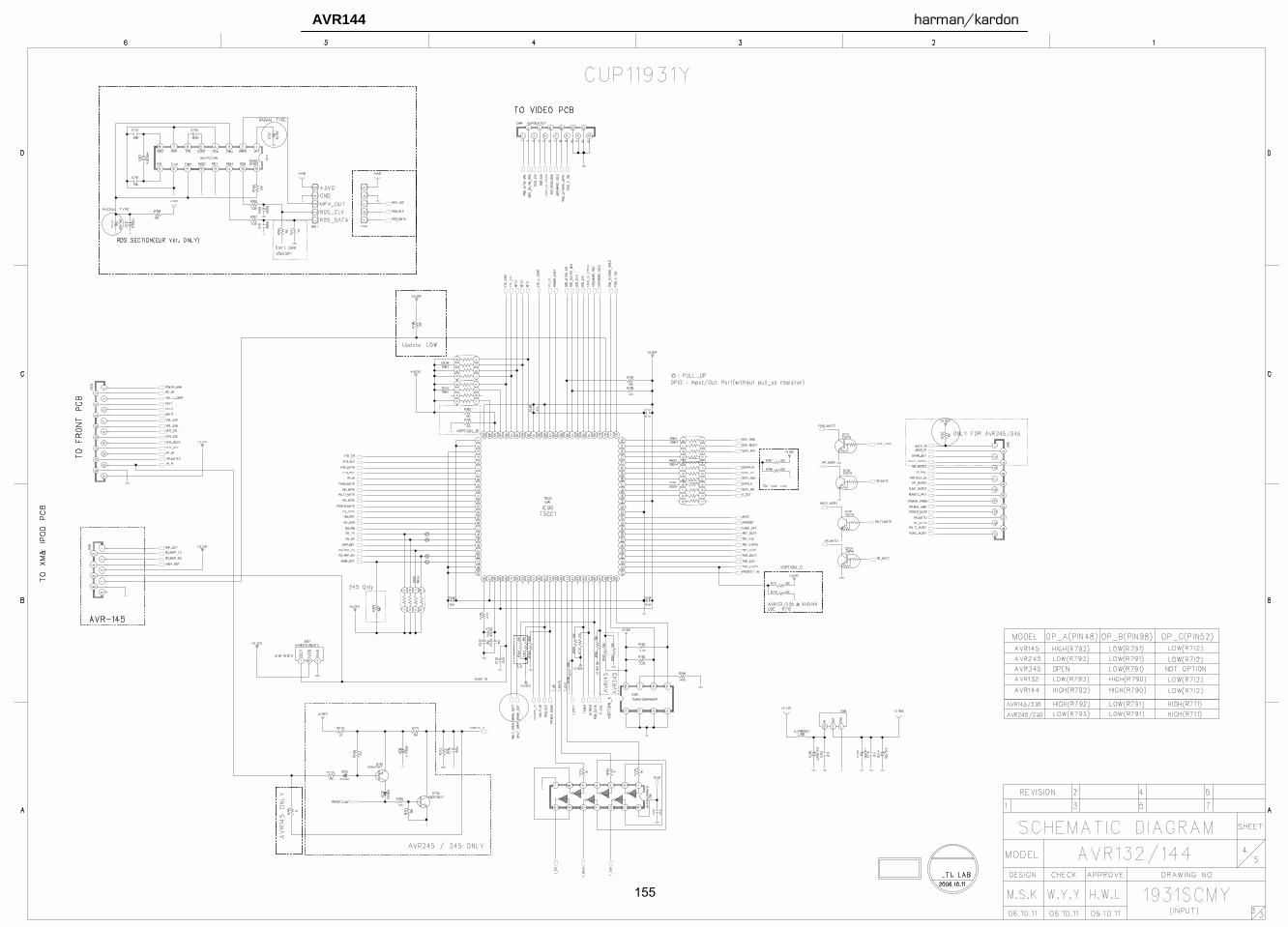
155
AVR144 harman/kardon

156
AVR144 harman/kardon
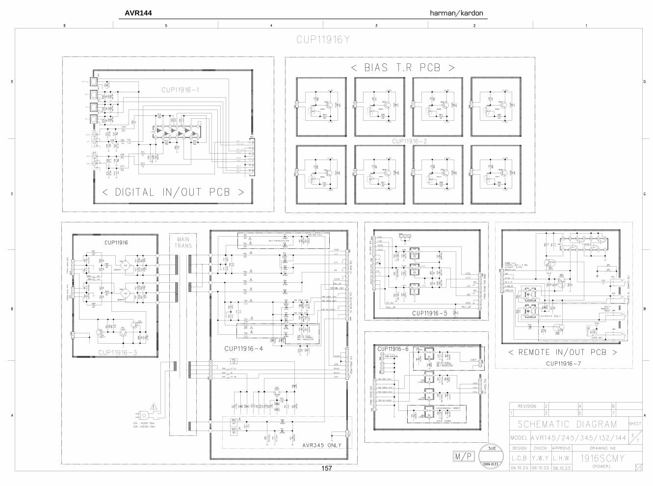
AVRx45 POWER(20061023)SCH.sch-1 - Mon Oct 23 17:14:10 2006
157
AVR144 harman/kardon

20061023_AVR132+144 WIRING.sch-1 - Mon Oct 23 16:15:57 2006
158
AVR144 harman/kardon
Related Documents