SERVICE MANUAL MICRO COMPONENT SYSTEM No.20917 Mar. 2001 COPYRIGHT 2001 VICTOR COMPANY OF JAPAN, LTD. UX-P5R UX-P5R Contents Safety precautions Preventing static electricity Important for laser products Disassembly method Main adjustment Flow of functional operation until TOC read (CD) Maintenance of laser pickup Replacement of laser pickup Description of major ICs Internal connection of display 1-2 1-4 1-6 1-7 1-15 1-19 1-20 1-20 1-21 1-40 This service manual is printed on 100% recycled paper. Area Suffix B E EN U.K. Continental Europe Northern Europe SLEEP MD/AUX FM/AM TAPE CD DISPLAY DIMMER REPEAT RANDOM PROG FM MODE AUTO PRESET SOUND MODE CD CANCEL MULTI KEY SET PTY /EON DISPLAY MODE RM-SUXP5R REMOTE CONTROL VOLUME AHB PRO CD TAPE FM/AM M I C R O C O M P O N E N T S Y S T E M U X · P 5 R CD-R/RW PLAYBACK MD/AUX TIMER CLOCK /VOLUME FUNCTION SOUND DIRECT OPERATING AHB PRO REC REV.MODE PHONES AUTO REVERSE REC /

Welcome message from author
This document is posted to help you gain knowledge. Please leave a comment to let me know what you think about it! Share it to your friends and learn new things together.
Transcript

1-1
UX-P5R
SERVICE MANUALMICRO COMPONENT SYSTEM
No.20917Mar. 2001
COPYRIGHT 2001 VICTOR COMPANY OF JAPAN, LTD.
UX-P5R
UX-P5R
ContentsSafety precautionsPreventing static electricityImportant for laser productsDisassembly methodMain adjustmentFlow of functional operation until TOC read (CD)
Maintenance of laser pickupReplacement of laser pickup Description of major ICsInternal connection of display
1-21-41-61-71-15
1-19
1-201-201-211-40
This service manual is printed on 100% recycled paper.
Area SuffixBEEN
U.K.Continental Europe
Northern Europe
SLEEP
STANDBY/ON
MD/AUX
FM/AM
TAPE
CD
DISPLAYDIMMER
REPEATRANDOMPROG
FM MODEAUTOPRESET
SOUNDMODE
CD
CANCEL MULTI KEY SET
PTY/EON
DISPLAYMODE
RM-SUXP5R REMOTE CONTROL
VOLUMEAHBPRO
COMPACT
DIGITAL AUDIO
CD TAPE FM/AM
M I C R O C O M P O N E N T S Y S T E M U X · P 5 R
C D - R / R W P L A Y B A C K
MD/AUX
TIMER
CLOCK
STANDBY/ON
STANDBY / ON
VOLUMEFUNCTIONSOUND
DIRECT OPERATING
AHB PRO
REC
REV.MODE
PHONES A U T O R E V E R S E
REC
/
1-2
UX-P5R
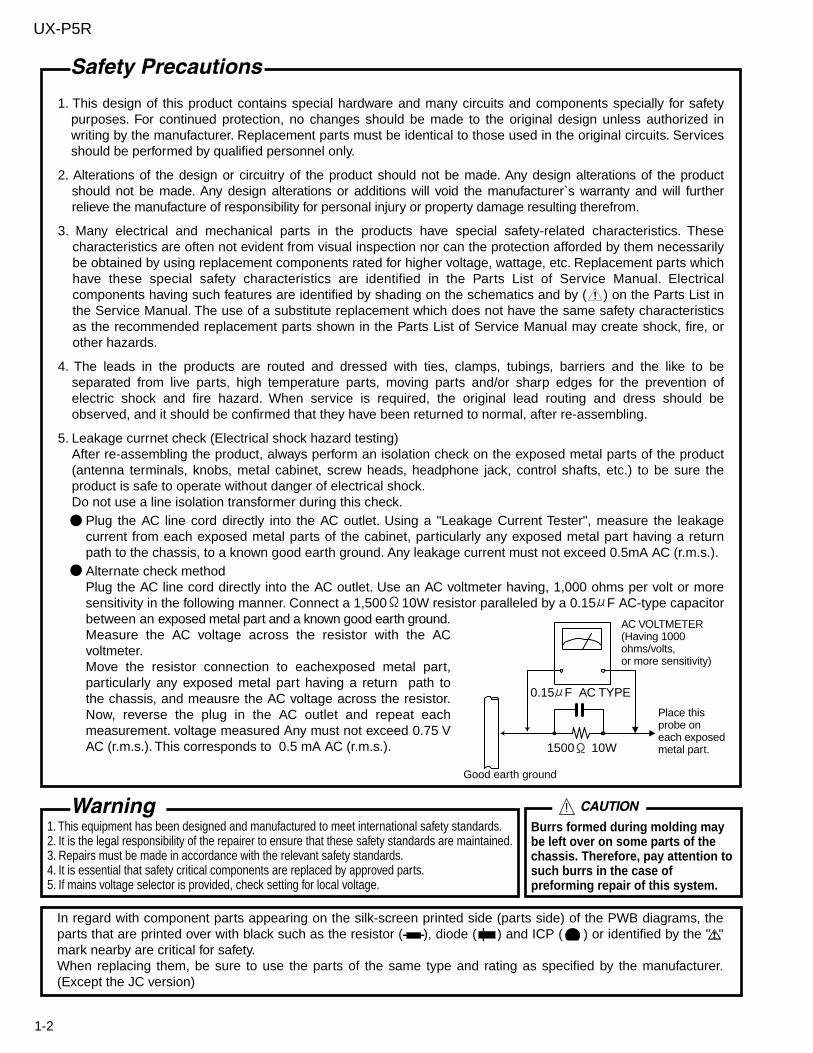
1. This design of this product contains special hardware and many circuits and components specially for safety purposes. For continued protection, no changes should be made to the original design unless authorized in writing by the manufacturer. Replacement parts must be identical to those used in the original circuits. Services should be performed by qualified personnel only.
2. Alterations of the design or circuitry of the product should not be made. Any design alterations of the product should not be made. Any design alterations or additions will void the manufacturer`s warranty and will further relieve the manufacture of responsibility for personal injury or property damage resulting therefrom.
3. Many electrical and mechanical parts in the products have special safety-related characteristics. These characteristics are often not evident from visual inspection nor can the protection afforded by them necessarily be obtained by using replacement components rated for higher voltage, wattage, etc. Replacement parts which have these special safety characteristics are identified in the Parts List of Service Manual. Electrical components having such features are identified by shading on the schematics and by ( ) on the Parts List in the Service Manual. The use of a substitute replacement which does not have the same safety characteristics as the recommended replacement parts shown in the Parts List of Service Manual may create shock, fire, or other hazards.
4. The leads in the products are routed and dressed with ties, clamps, tubings, barriers and the like to be separated from live parts, high temperature parts, moving parts and/or sharp edges for the prevention of electric shock and fire hazard. When service is required, the original lead routing and dress should be observed, and it should be confirmed that they have been returned to normal, after re-assembling.
5. Leakage currnet check (Electrical shock hazard testing)After re-assembling the product, always perform an isolation check on the exposed metal parts of the product (antenna terminals, knobs, metal cabinet, screw heads, headphone jack, control shafts, etc.) to be sure the product is safe to operate without danger of electrical shock.Do not use a line isolation transformer during this check.
Plug the AC line cord directly into the AC outlet. Using a "Leakage Current Tester", measure the leakage current from each exposed metal parts of the cabinet, particularly any exposed metal part having a return path to the chassis, to a known good earth ground. Any leakage current must not exceed 0.5mA AC (r.m.s.).Alternate check methodPlug the AC line cord directly into the AC outlet. Use an AC voltmeter having, 1,000 ohms per volt or more sensitivity in the following manner. Connect a 1,500 10W resistor paralleled by a 0.15 F AC-type capacitor between an exposed metal part and a known good earth ground.Measure the AC voltage across the resistor with the AC voltmeter. Move the resistor connection to eachexposed metal part, particularly any exposed metal part having a return path to the chassis, and meausre the AC voltage across the resistor. Now, reverse the plug in the AC outlet and repeat each measurement. voltage measured Any must not exceed 0.75 V AC (r.m.s.). This corresponds to 0.5 mA AC (r.m.s.).
1. This equipment has been designed and manufactured to meet international safety standards.2. It is the legal responsibility of the repairer to ensure that these safety standards are maintained.3. Repairs must be made in accordance with the relevant safety standards.4. It is essential that safety critical components are replaced by approved parts.5. If mains voltage selector is provided, check setting for local voltage.
Good earth ground
Place this probe on each exposedmetal part.
AC VOLTMETER(Having 1000 ohms/volts,or more sensitivity)
1500 10W
0.15 F AC TYPE
!Burrs formed during molding may be left over on some parts of the chassis. Therefore, pay attention to such burrs in the case of preforming repair of this system.
In regard with component parts appearing on the silk-screen printed side (parts side) of the PWB diagrams, the parts that are printed over with black such as the resistor ( ), diode ( ) and ICP ( ) or identified by the " " mark nearby are critical for safety. When replacing them, be sure to use the parts of the same type and rating as specified by the manufacturer. (Except the JC version)
1-3
UX-P5R
1. Service should be performed by qualified personnel only.2. This equipment has been designed and manufactured to meet international safety standards.3. It is the legal responsibility of the repairer to ensure that these safety standards are maintained.4. Repairs must be made in accordance with the relevant safety standards.5. It is essential that safety critical components are replaced by approved parts.6. If mains voltage selector is provided, check setting for local voltage.
1. This design of this product contains special hardware and many circuits and components specially for safety purposes. For continued protection, no changes should be made to the original design unless authorized in writing by the manufacturer. Replacement parts must be identical to those used in the original circuits.
2. Any unauthorised design alterations or additions will void the manufacturer's guarantee ; furthermore the manufacturer cannot accept responsibility for personal injury or property damage resulting therefrom.
3. Essential safety critical components are identified by ( ) on the Parts List and by shading on the schematics, and must never be replaced by parts other than those listed in the manual. Please note however that many electrical and mechanical parts in the product have special safety related characteristics. These characteristics are often not evident from visual inspection. Parts other than specified by the manufacturer may not have the same safety characteristics as the recommended replacement parts shown in the Parts List of the Service Manual and may create shock, fire, or other hazards.
4. The leads in the products are routed and dressed with ties, clamps, tubings, barriers and the like to be separated from live parts, high temperature parts, moving parts and/or sharp edges for the prevention of electric shock and fire hazard. When service is required, the original lead routing and dress should be observed, and it should be confirmed that they have been returned to normal, after re-assembling.
! Burrs formed during molding may be left over on some parts of the chassis. Therefore, pay attention to such burrs in the case of preforming repair of this system.
(U.K only)
1-4
UX-P5R
Preventing static electricityElectrostatic discharge (ESD), which occurs when static electricity stored in the body, fabric, etc. is discharged, can destroy the laser diode in the traverse unit (optical pickup). Take care to prevent this when performing repairs.
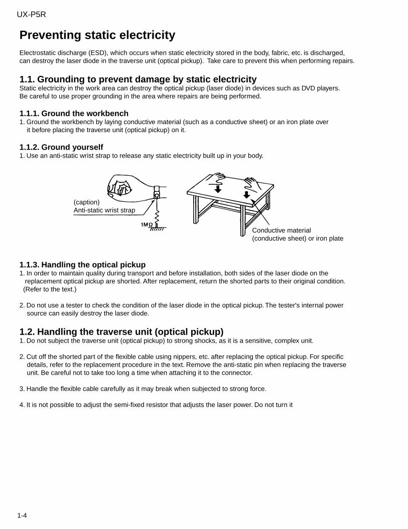
1.1. Grounding to prevent damage by static electricityStatic electricity in the work area can destroy the optical pickup (laser diode) in devices such as DVD players. Be careful to use proper grounding in the area where repairs are being performed.
1.1.1. Ground the workbench1. Ground the workbench by laying conductive material (such as a conductive sheet) or an iron plate over it before placing the traverse unit (optical pickup) on it.
1.1.2. Ground yourself1. Use an anti-static wrist strap to release any static electricity built up in your body.
1.1.3. Handling the optical pickup1. In order to maintain quality during transport and before installation, both sides of the laser diode on the replacement optical pickup are shorted. After replacement, return the shorted parts to their original condition. (Refer to the text.)
2. Do not use a tester to check the condition of the laser diode in the optical pickup. The tester's internal power source can easily destroy the laser diode.
1.2. Handling the traverse unit (optical pickup)1. Do not subject the traverse unit (optical pickup) to strong shocks, as it is a sensitive, complex unit.
2. Cut off the shorted part of the flexible cable using nippers, etc. after replacing the optical pickup. For specific details, refer to the replacement procedure in the text. Remove the anti-static pin when replacing the traverse unit. Be careful not to take too long a time when attaching it to the connector.
3. Handle the flexible cable carefully as it may break when subjected to strong force.
4. It is not possible to adjust the semi-fixed resistor that adjusts the laser power. Do not turn it
Conductive material (conductive sheet) or iron plate
(caption)Anti-static wrist strap
1-5
UX-P5R
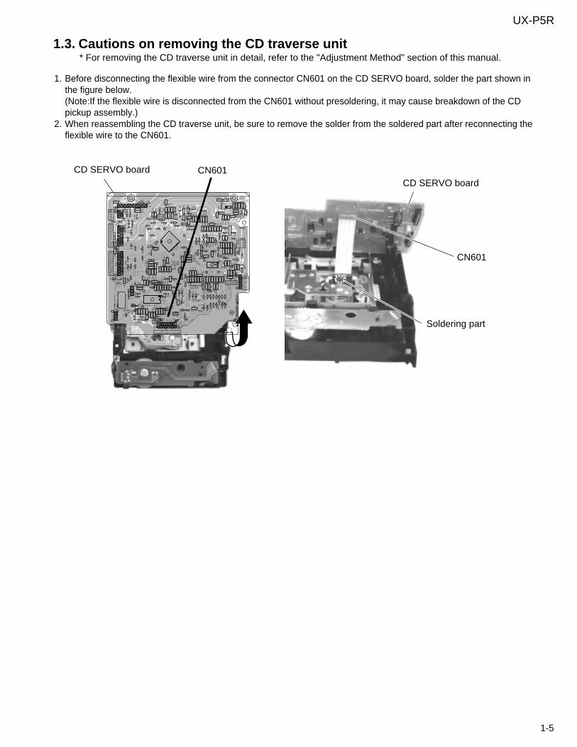
1.3. Cautions on removing the CD traverse unit* For removing the CD traverse unit in detail, refer to the "Adjustment Method" section of this manual.
1. Before disconnecting the flexible wire from the connector CN601 on the CD SERVO board, solder the part shown in the figure below.(Note:If the flexible wire is disconnected from the CN601 without presoldering, it may cause breakdown of the CD pickup assembly.)
2. When reassembling the CD traverse unit, be sure to remove the solder from the soldered part after reconnecting the flexible wire to the CN601.
CD SERVO boardCD SERVO board
Soldering part
CN601
CN601
C60
1
C60
2C
603
C60
4
C60
5
C60
6
C60
7
C610
C61
1
C61
2
C61
3
C61
4
C61
5
C61
6
C617
C61
9C
620
C62
1
C62
2
C62
3
C624
C63
1
C63
2
C633
C64
1
C64
2
C643
B619
C65
1
C65
2
C65
3
C65
4
C655
C65
6
C65
7
C65
8
C66
1
C66
3
C66
4C
665
C66
7
C66
8
C669
C670
C671
C672
C67
3
C67
6
C67
7 C679
C68
0
C69
1
C69
2
C69
3
C694
C69
5
C69
6
C69
9
C80
1
C80
2
C81
1
C812
C813
C81
4
C81
5
C82
1
C82
2
C82
3
C824
C83
1
C832
C833
CN601
CN
651
CN
652
CN801
D831
R64
8
IC652
IC80
1
IC802
L831
Q63
1
Q80
1
R60
1R
602
R60
3
R60
4
R60
5R
606
R61
0R
611
R61
2R
613
R61
7
R61
8
R61
9
R62
0
R62
1
R63
1
R63
2
R63
4R
635
R636
R64
1R
642
R64
3
R64
7
R65
1R
652
R65
3
R65
4
R65
5R
656
R65
7
R65
8
R65
9
R66
1
R66
2
R66
3R
664
R66
5
R66
6
R667R
668
R66
9
R67
0
R68
2
R683
R68
5
R69
1
R69
2
R69
5R
696
R70
1
R70
2
R70
3
R70
4
R70
5
R70
6
R707
R708
R709
R710
R80
1R
802
R80
3R
804
R80
5
R80
6
R80
7
R80
8
R80
9
R81
2
R821
R82
2
R82
3
R82
4
R83
1
W60
5
CN606
X651
B604
B616
B614
R81
3
C81
6
B613
B615
B610
B612
B617
B618
IC601
R60
7
B601
B603
B602
B611
B609
B608
B607
B606
B605
D601
D60
2
R681
C68
1
R684
MUTEFLAG
CDDG
BLKCK/RESTMLDMDATAMCLKCDDGSUBQSQCK/RSTSTAT
FM+RESTSM-SM+D.GNDFM-
1
1
1
1
1
BE
BE
C
31
6ARF
A.GND
F- T- T+ F+ GN
DVR LD M
DT2 K F1 N
CT1 SR F2
1 15
T02
SCDSCD
CDDG
13
LM+OPSWGNDCLSWLM-
M.GNDSW10SW10CLOSEOPENOPSWCLSECD+BCD+BCDLA.GNDA.GNDCDR
51
116
1
21
41
61
17
16
32
12
2413
1-6
UX-P5R
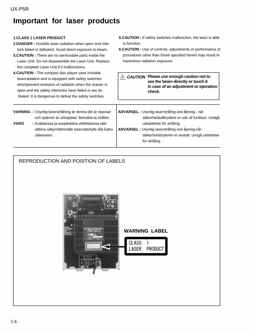
Important for laser products
1.CLASS 1 LASER PRODUCT
2.DANGER : Invisible laser radiation when open and inter
lock failed or defeated. Avoid direct exposure to beam.
3.CAUTION : There are no serviceable parts inside the
Laser Unit. Do not disassemble the Laser Unit. Replace
the complete Laser Unit if it malfunctions.
4.CAUTION : The compact disc player uses invisible
laserradiation and is equipped with safety switches
whichprevent emission of radiation when the drawer is
open and the safety interlocks have failed or are de
feated. It is dangerous to defeat the safety switches.
5.CAUTION : If safety switches malfunction, the laser is able
to function.
6.CAUTION : Use of controls, adjustments or performance of
procedures other than those specified herein may result in
hazardous radiation exposure.
VARNING : Osynlig laserstrålning är denna del är öppnad
och spårren är urkopplad. Betrakta ej strålen.
VARO : Avattaessa ja suojalukitus ohitettaessa olet
alttiina näkymättömälle lasersäteilylle.Älä katso
säteeseen.
ADVARSEL : Usynlig laserstråling ved åbning , når
sikkerhedsafbrydere er ude af funktion. Undgå
udsættelse for stråling.
ADVARSEL : Usynlig laserstråling ved åpning,når
sikkerhetsbryteren er avslott. unngå utsettelse
for stråling.
REPRODUCTION AND POSITION OF LABELS
WARNING LABEL
! CAUTION Please use enough caution not to see the beam directly or touch it in case of an adjustment or operationcheck.
1-7
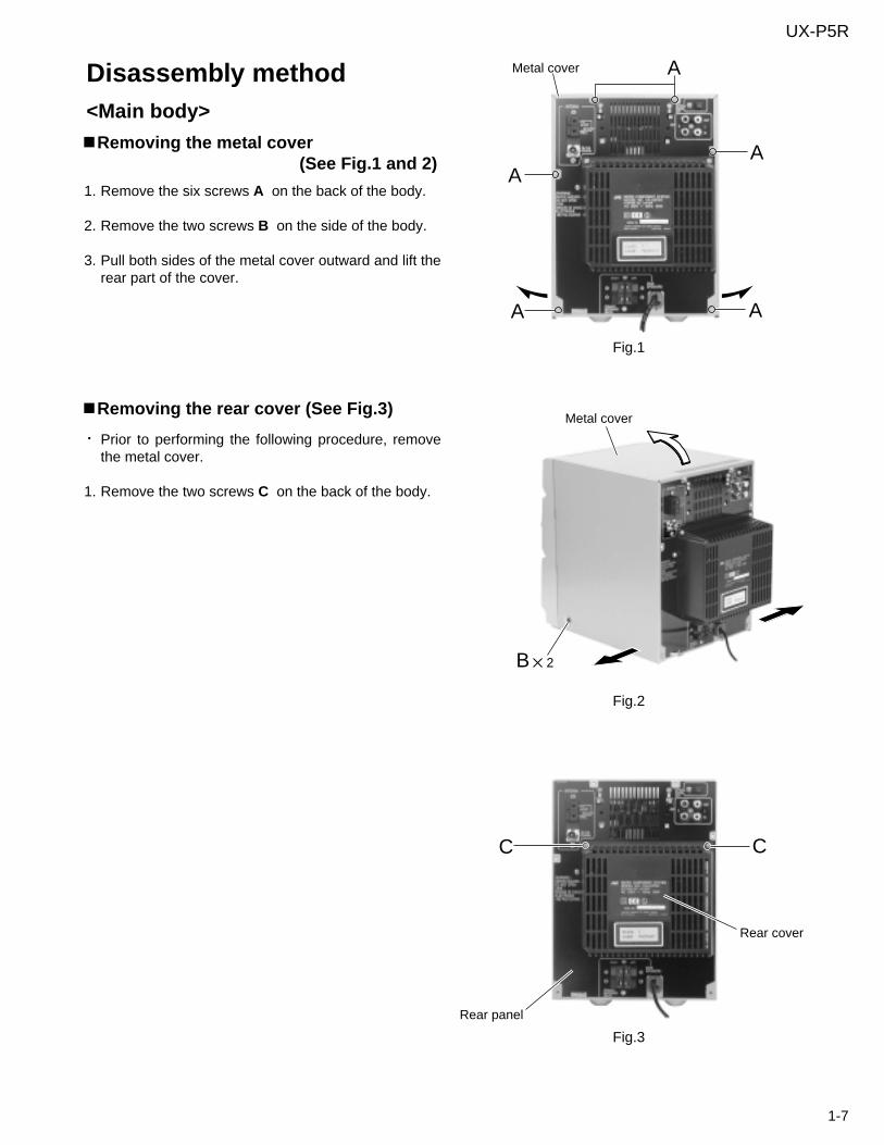
UX-P5R
Remove the six screws A on the back of the body.
Remove the two screws B on the side of the body.
Pull both sides of the metal cover outward and lift the rear part of the cover.
1.
2.
3.
Disassembly method<Main body>
Removing the metal cover (See Fig.1 and 2)
Prior to performing the following procedure, remove the metal cover.
Remove the two screws C on the back of the body.1.
Removing the rear cover (See Fig.3)
Fig.1
Fig.2
Fig.3
A
A
A
A
A
Metal cover
Metal cover
B 2
C
Rear cover
Rear panel
C
1-8
UX-P5R
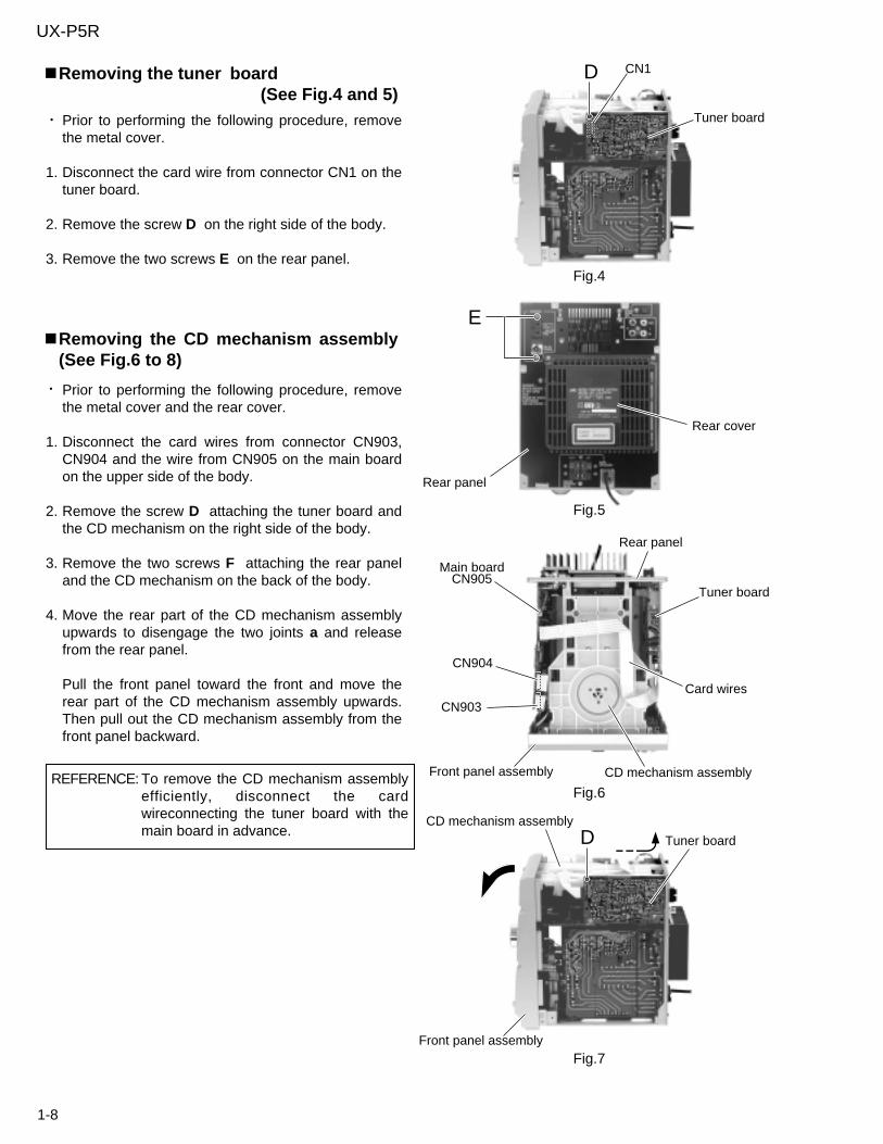
Prior to performing the following procedure, remove the metal cover.
Disconnect the card wire from connector CN1 on the tuner board.
Remove the screw D on the right side of the body.
Remove the two screws E on the rear panel.
1.
2.
3.
Removing the tuner board (See Fig.4 and 5)
Prior to performing the following procedure, remove the metal cover and the rear cover.
Disconnect the card wires from connector CN903, CN904 and the wire from CN905 on the main board on the upper side of the body.
Remove the screw D attaching the tuner board and the CD mechanism on the right side of the body.
Remove the two screws F attaching the rear panel and the CD mechanism on the back of the body.
Move the rear part of the CD mechanism assembly upwards to disengage the two joints a and release from the rear panel.
Pull the front panel toward the front and move the rear part of the CD mechanism assembly upwards. Then pull out the CD mechanism assembly from the front panel backward.
1.
2.
3.
4.
Removing the CD mechanism assembly (See Fig.6 to 8)
To remove the CD mechanism assembly efficiently, disconnect the card wireconnecting the tuner board with the main board in advance.
REFERENCE:
Fig.4
Fig.5
Fig.6
Fig.7
D CN1
Tuner board
E
Rear cover
Rear panel
Rear panel
Tuner board
Card wires
CD mechanism assemblyFront panel assembly
CN903
CN904
Main boardCN905
CD mechanism assembly
Tuner boardD
Front panel assembly
1-9
UX-P5R
Prior to performing the following procedure, remove the metal cover, rear cover and the CD mechanism assembly.
Remove the seven screws G attaching the rear panel.
Disconnect the card wire from CN902 on the main board.
Disengage the lower two joints b on each side of the rear panel using a screwdriver and remove the rear panel backward (The tuner board and the fan will be also detached.Remove them as needed).
1.
2.
3.
Remove the rear panel (See Fig.8 to 11)
Prior to performing the following procedure, remove the metal cover, the rear cover andthe CD mechanism assembly.
Disconnect the wire from connector CN908 on the main board.
Remove the two screws H on the back of the body.
Move the fan upwards to disengage the four joints c and release from the rear panel.
1.
2.
3.
Removing the fan (See Fig.9 and 12)
Fig.8
Fig.9
Fig.10
Fig.11Fig.12
F
G
G
G
G
Rear panel
Joint aJoint a
Joint bRear panel
Rear panelJoint b
Fan
Rear panel
H H
Joint c
Joint c
Joint c
Joint c
Main boardCN908
CN902 FanRear panel
Tuner board
1-10
UX-P5R
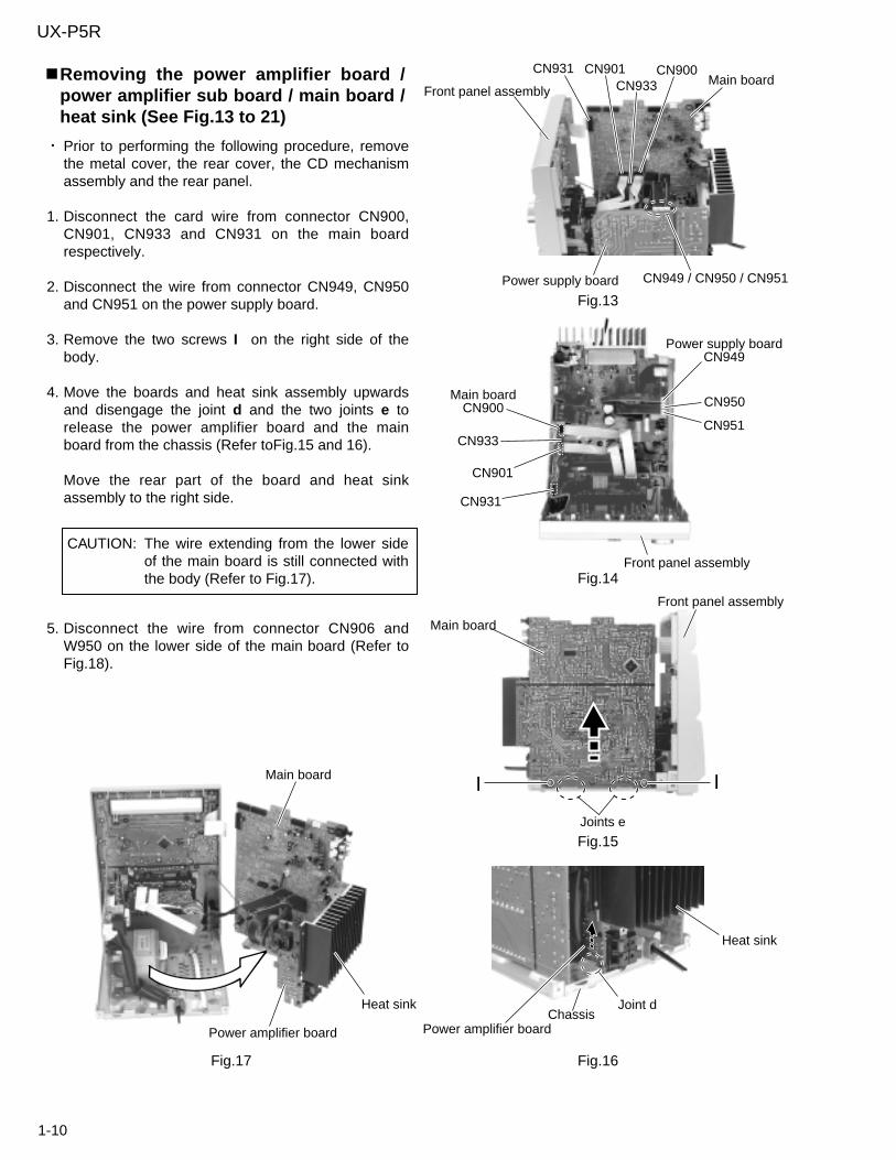
Prior to performing the following procedure, remove the metal cover, the rear cover, the CD mechanism assembly and the rear panel.
Disconnect the card wire from connector CN900, CN901, CN933 and CN931 on the main board respectively.
Disconnect the wire from connector CN949, CN950 and CN951 on the power supply board.
Remove the two screws I on the right side of the body.
Move the boards and heat sink assembly upwards and disengage the joint d and the two joints e to release the power amplifier board and the main board from the chassis (Refer toFig.15 and 16).
Move the rear part of the board and heat sink assembly to the right side.
1.
2.
3.
4.
Removing the power amplifier board / power amplifier sub board / main board / heat sink (See Fig.13 to 21)
The wire extending from the lower side of the main board is still connected with the body (Refer to Fig.17).
CAUTION:
Disconnect the wire from connector CN906 and W950 on the lower side of the main board (Refer to Fig.18).
5.
Fig.13
Fig.14
Fig.15
Fig.16Fig.17
CN931 CN901CN933
CN900Main board
Front panel assembly
Power supply board CN949 / CN950 / CN951
Power supply boardCN949
CN951
Main boardCN900
CN933
CN931
Front panel assembly
Front panel assembly
Main board
I I
Joints e
Joint d
Heat sink
ChassisPower amplifier board
Main board
Heat sink
Power amplifier board
CN901
CN950
1-11
UX-P5R
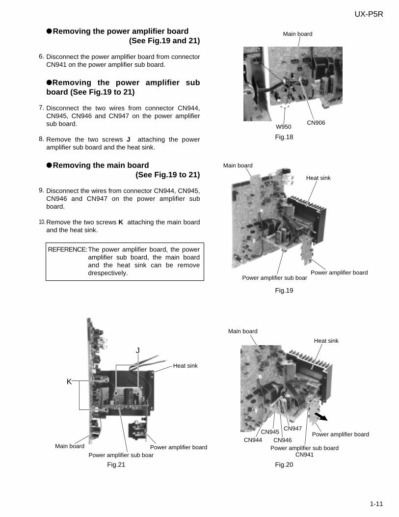
Removing the power amplifier board (See Fig.19 and 21)
Disconnect the power amplifier board from connector CN941 on the power amplifier sub board.
6.
The power amplifier board, the power amplifier sub board, the main board and the heat sink can be remove drespectively.
REFERENCE:
Removing the power amplifier sub board (See Fig.19 to 21)
Disconnect the two wires from connector CN944, CN945, CN946 and CN947 on the power amplifier sub board.
Remove the two screws J attaching the power amplifier sub board and the heat sink.
7.
8.
Removing the main board (See Fig.19 to 21)
Disconnect the wires from connector CN944, CN945, CN946 and CN947 on the power amplifier sub board.
Remove the two screws K attaching the main board and the heat sink.
9.
10.
Fig.18
Fig.19
Fig.20Fig.21
CN906W950
Main board
Heat sink
Power amplifier board
Main board
Power amplifier sub boar
Heat sink
Power amplifier board
Main board
Power amplifier sub boardCN941
CN947
CN946CN944
Heat sink
K
Power amplifier boardMain board
Power amplifier sub boar
CN945
J
1-12
UX-P5R
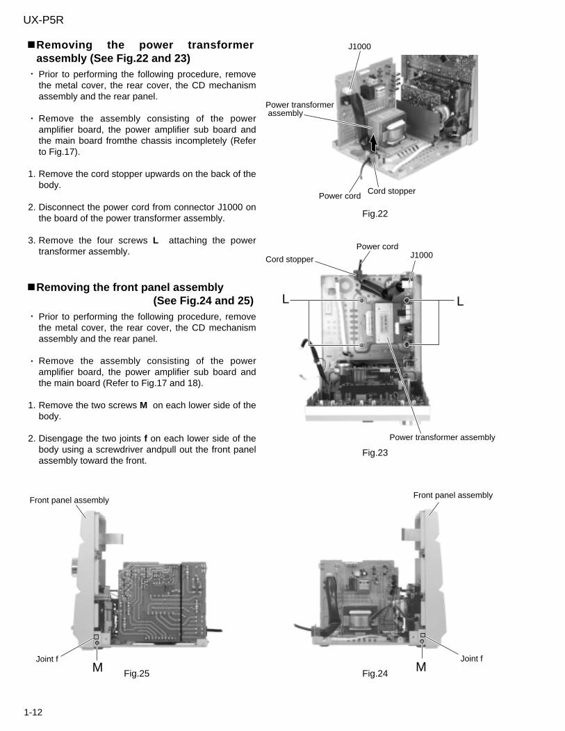
Prior to performing the following procedure, remove the metal cover, the rear cover, the CD mechanism assembly and the rear panel.
Remove the assembly consisting of the power amplifier board, the power amplifier sub board and the main board fromthe chassis incompletely (Refer to Fig.17).
Remove the cord stopper upwards on the back of the body.
Disconnect the power cord from connector J1000 on the board of the power transformer assembly.
Remove the four screws L attaching the power transformer assembly.
1.
2.
3.
Removing the power transformer assembly (See Fig.22 and 23)
Prior to performing the following procedure, remove the metal cover, the rear cover, the CD mechanism assembly and the rear panel.
Remove the assembly consisting of the power amplifier board, the power amplifier sub board and the main board (Refer to Fig.17 and 18).
Remove the two screws M on each lower side of the body.
Disengage the two joints f on each lower side of the body using a screwdriver andpull out the front panel assembly toward the front.
1.
2.
Removing the front panel assembly (See Fig.24 and 25)
Fig.22
Fig.23
Fig.24Fig.25
J1000
Power transformer assembly
Cord stopperPower cord
Power cord
Cord stopper J1000
L L
Power transformer assembly
Front panel assemblyFront panel assembly
M MJoint f Joint f
1-13
UX-P5R
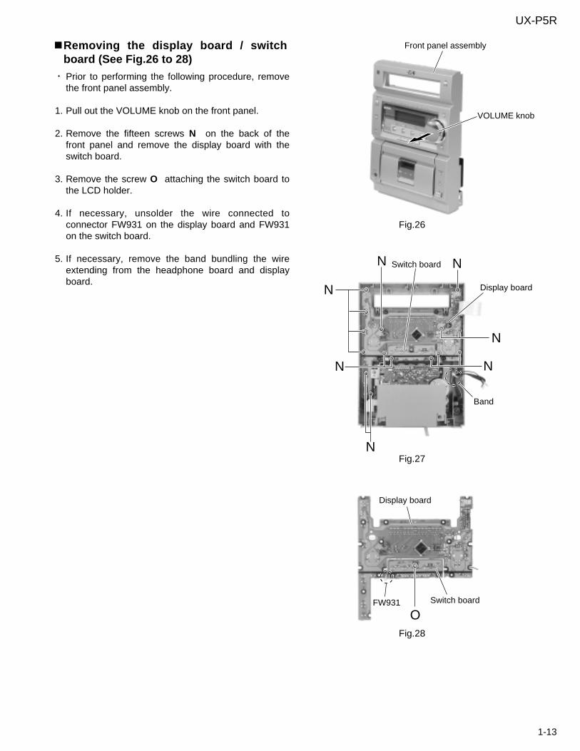
Prior to performing the following procedure, remove the front panel assembly.
Pull out the VOLUME knob on the front panel.
Remove the fifteen screws N on the back of the front panel and remove the display board with the switch board.
Remove the screw O attaching the switch board to the LCD holder.
If necessary, unsolder the wire connected to connector FW931 on the display board and FW931 on the switch board.
If necessary, remove the band bundling the wire extending from the headphone board and display board.
1.
2.
3.
4.
5.
Removing the display board / switch board (See Fig.26 to 28)
Fig.26
Fig.27
Fig.28
Front panel assembly
VOLUME knob
Display board
Switch boardN N
N
N
N
N
N
Band
Switch board
Display board
FW931
O
1-14
UX-P5R
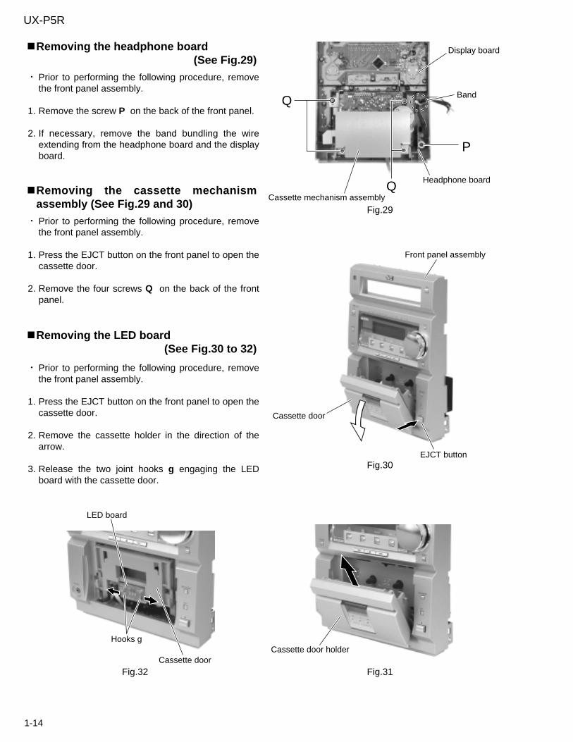
Prior to performing the following procedure, remove the front panel assembly.
Remove the screw P on the back of the front panel.
If necessary, remove the band bundling the wire extending from the headphone board and the display board.
1.
2.
Removing the headphone board (See Fig.29)
Prior to performing the following procedure, remove the front panel assembly.
Press the EJCT button on the front panel to open the cassette door.
Remove the four screws Q on the back of the front panel.
1.
2.
Removing the cassette mechanism assembly (See Fig.29 and 30)
Prior to performing the following procedure, remove the front panel assembly.
Press the EJCT button on the front panel to open the cassette door.
Remove the cassette holder in the direction of the arrow.
Release the two joint hooks g engaging the LED board with the cassette door.
1.
2.
3.
Removing the LED board (See Fig.30 to 32)
Fig.29
Fig.30
Fig.31Fig.32
Display board
Q
Band
P
Headphone board
Cassette mechanism assembly
Q
Front panel assembly
Cassette door
EJCT button
Cassette door holderCassette door
LED board
Hooks g
1-15
UX-P5R
Main adjustment
Measurement Instruments Required for Adjustment 1. Low frequency oscillator This oscillator should have a capacity to output 0dBs to 600 at an oscillation frequency of 50Hz-20kHz. 2. Attenuator impedance : 600 3. Electronic voltmeter 4. Distortion meter 5. Frequency counter 6. Wow & flutter meter 7. Test tape VTT703L : Head azimuth VT712 : Tape speed and running unevenness (3kHz) VT724 : Reference level (1kHz) 8. Blank tape TYPE : AC-225 TYPE : AC-514 9. Torque gauge : For play and back tension FWD(TW2111A), REV(TW2121a) and FF/REW(TW2231A)10. Test disc: CTS-1000
Radio Input signal
AM frequency --------------------------------------- 400Hz AM modulation ---------------------------------------- 30% FM frequency --------------------------------------- 400Hz FM frequency deviation ------------------------ 22.5kHz
Tuner section
B/E/EN version FM Band cover: 87.5 108MHz MW Band cover: 522 1,629kHz LW Band cover: 144 288kHz EE version FM Band cover: 65 74MHz, 87.5 108MHz MW Band cover: 522 1,629kHz LW Band cover: 144 288kHz UB/UF/US/UX/U version FM Band cover: 87.5 108MHz MW Band cover: 531 1,602kHz, 530 1,710kHz SW Band cover: SW1 2.3 6.995MHz : SW2 7 21.85MHz Voltage applied to tuner +B : DC5.7V VT : DC 12V Reference measurement output 26.1mV(0.28V)/3 Input positions AM : Standard loop antenna FM : TP1 (hot) and TP2 (GND)
Standard measurement position of volume
Function switch to Tape Beat cut switch to Cut Super Bass/Active hyper Bass to OFF Bass Treble to Center Adjustment of main volume to reference output VOL : 28Precautions for measurement1. Apply 30pF and 33k to the IF sweeper output side and 0.082 F and 100k in series to the sweeper input side.2. The IF sweeper output level should be made as low as possible within the adjustable range.3. Since the IF sweeper is a fixed device, there is no need to adjust this sweeper.4. Since a ceramic oscillator is used, there is no need to perform any MIX adjustment.5. Since a fixed coil is used, there is no need to adjust the FM tracking.6. The input and output earth systems are separated. In case of simultaneously measuring the voltage in both of the input and output systems with an electronic voltmeter for two channels, therefore, the earth should be connected particularly carefully.7. In the case of BTL connection amp., the minus terminal of speaker is not for earthing. Therefore, be sure not to connect any other earth terminal to this terminal. This system is of an BTL system.8. For connecting a dummy resistor when measuring the output, use the wire with a greater code size.9. Whenever any mixed tape is used, use the band pass filter (DV-12).
Measurement conditions Power supply voltage : AC230V (50Hz)----B/E/EE/EN : AC110/127V/230V(50/60Hz) : UB/UF/US/UX/U Reference output : Speaker : 0.775V/4 : Headphone : 0.077V/32 Reference frequency and input level ------------------------------ 1kHz, AUX : -8dBs MIX MIC: -54dBs (UB/UF/US/UX/U) Input for confirming recording and playback characteristics ------------------------- AUX : -28dBs Measurement output terminal ------- at Speaker J3002 Load resistance --------------------------- 4
1-16
UX-P5R
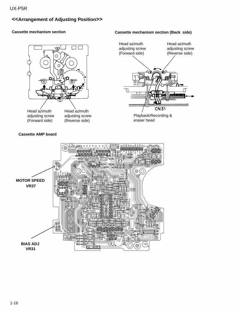
<<Arrangement of Adjusting Position>>
Cassette mechanism section Cassette mechanism section (Back side)
Head azimuthadjusting screw(Reverse side)
Head azimuthadjusting screw(Forward side)
Playback/Recording & eraser head
Head azimuthadjusting screw(Forward side)
Head azimuthadjusting screw(Reverse side)
C202
C376
C10
3
C121
C106
C305
C108
C109
C107
C30
8
R20
3
C30
2
C20
3
R109
C206
R10
4
C209
C113
R209
C207
C301
C31
0
C30
3
C304
C208
C331
C31
3
R11
6
R20
4
C316
B10
6
C319
R10
3
C375
61
CN31
B158
70u
FRE
PLA
PH
O5VM
GS
OL
RR
ETA
PN
C
1 10
CN32
9 1IC31
8 9IC
32
1 16
16
1 8
9IC33
L301
Q10
1
Q20
1
Q30
5
Q302
B16
8
C334
BQ375E
Q376
Q371
B
E
C201
R101
R10
2C
104
R105
R10
6
R107
R10
8
C22
1
R110R111R112
R121
R201
R20
2C
204
R205
R20
6
R207
R208
C11
1
R210R211R212
R221
R30
1
R30
3
R30
4
B16
7
R33
5
R31
5
R31
4
R31
3
R31
0
R122
Q10
3
R305
B15
1
R371
R375 R37
6
R372
R33
8R
337
R34
1
R34
2
R34
3
R339
R33
6
R33
1
VR
31V
R37
C210C110
C102 C101
Q372
C213
C211
R215
D375
R115
R34
0
Q331
B11
3
R345
9
CN
33
11
CN34
MS M
B
PB
RA
GPB
LS
W8V
RE
CR
AGRE
CL
MG
10
R327
C306
R21
6
C37
1
B15
3
B152
B162
C37
4
R222
B102
B20
0
B10
1
Q203
B110
B109B108
B164
B16
1
B163
R353
B155
C31
7
C314
L303
R373
B15
7
B15
9
B156
B160
B11
2
C307
B16
6
Q32
1
B198C105
C20
5
C33
2C
333
MOTOR SPEEDVR37
BIAS ADJVR31
Cassette AMP board
1-17
UX-P5R
Tape Recorder Section
Reference Values for Confirmation Items
Items
Items
Measurement conditions
Measurement conditions
Measurement method
Measurement method
Standard Values
Standard Values
Adjusting positions
Adjusting positions
Confirmationof head angle
Confirmationof tape speed
Test tape: VTT703L (8kHz)Measurement outputterminal: Speaker terminalSpeaker R(Load resistance: 4 ): Headphone terminal
1 Playback the test tape VTT703L (8kHz) 2 With the recording & playback mechanism, adjust the head azimuth screw so that the forward and reverse output levels become maximum. After adjustment, lock the head azimuth at least by half turn. 3 In either case, this adjustment should be performed in both the forward and reverse directions with the head azimuth screw.
Maximumoutput
Tape speedof deck: 2,940 ~ 3,090Hz
Adjust the headazimuth screwonly when thehead has beenchanged.
Test tape: VT712 (3kHz)Measurement outputterminal: Headphone terminal
When the test tape VT712 (3kHz) has beenplayed back with the recording and playback mechanism at the beginning of forward winding, the frequency counter reading of thedifference between both of the mechanismshould be 6.0Hz or less.
Adjust VR37 so that the frequency counterreading becomes 2,940~3,090Hz when playing back the test tape VT712 (3kHz) withplayback and recording mechanism afterending forward winding of the tape.
VR37
Differencebetween theforward andreverse speed
Test tape: VT712 (3kHz) Measurement outputterminal: Speaker terminalSpeaker R(Load resistance: 4 )Measurement outputterminal: Headphone
6.0Hz orless
Head azimuthscrew
Wow & flutter Test tape: VT712 (3kHz) Measurement outputterminal: Headphone terminal
When the test tape VT712 (3kHz) has beenplayed back with the recording and playbackmechanism at the beginning of forward winding, the frequency counter reading of wow & flutter should be 0.25% or less(WRMS).
0.25% orless(WRMS)
1-18
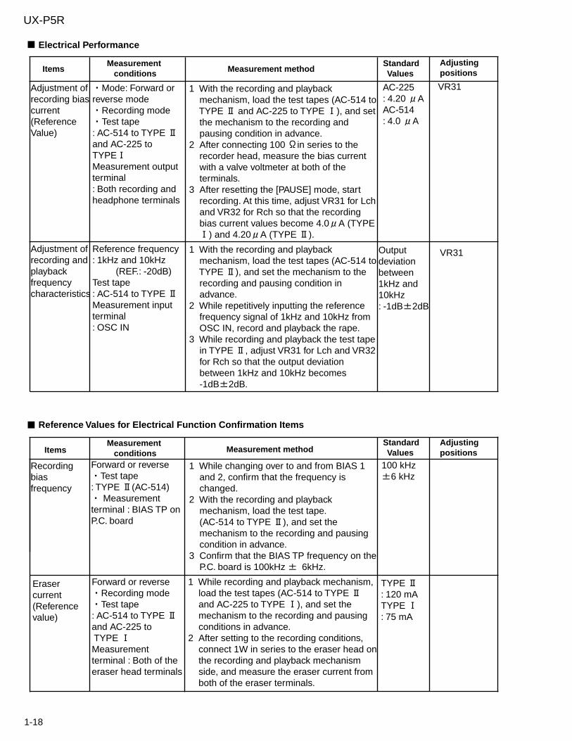
UX-P5R
Electrical Performance
Reference Values for Electrical Function Confirmation Items
Items
Items
Measurement conditions
Measurement conditions
Measurement method
Measurement method
Standard Values
Standard Values
Adjusting positions
Adjusting positions
Adjustment ofrecording andplaybackfrequencycharacteristics
Adjustment ofrecording biascurrent(ReferenceValue)
Reference frequency: 1kHz and 10kHz (REF.: -20dB)Test tape: AC-514 to TYPE Measurement inputterminal: OSC IN
Mode: Forward orreverse mode
Recording modeTest tape
: AC-514 to TYPE and AC-225 to TYPEMeasurement outputterminal: Both recording andheadphone terminals
1 With the recording and playback mechanism, load the test tapes (AC-514 to TYPE and AC-225 to TYPE ), and set the mechanism to the recording and pausing condition in advance. 2 After connecting 100 in series to the recorder head, measure the bias current with a valve voltmeter at both of the terminals. 3 After resetting the [PAUSE] mode, start recording. At this time, adjust VR31 for Lch and VR32 for Rch so that the recording bias current values become 4.0 A (TYPE ) and 4.20 A (TYPE ).
1 With the recording and playback mechanism, load the test tapes (AC-514 to TYPE ), and set the mechanism to the recording and pausing condition in advance. 2 While repetitively inputting the reference frequency signal of 1kHz and 10kHz from OSC IN, record and playback the rape. 3 While recording and playback the test tape in TYPE , adjust VR31 for Lch and VR32 for Rch so that the output deviation between 1kHz and 10kHz becomes -1dB 2dB.
1 While recording and playback mechanism, load the test tapes (AC-514 to TYPE and AC-225 to TYPE ), and set the mechanism to the recording and pausing conditions in advance. 2 After setting to the recording conditions, connect 1W in series to the eraser head on the recording and playback mechanism side, and measure the eraser current from both of the eraser terminals.
1 While changing over to and from BIAS 1 and 2, confirm that the frequency is changed. 2 With the recording and playback mechanism, load the test tape. (AC-514 to TYPE ), and set the mechanism to the recording and pausing condition in advance. 3 Confirm that the BIAS TP frequency on the P.C. board is 100kHz 6kHz.
Recordingbias frequency
Forward or reverseTest tape
: TYPE (AC-514) Measurement
terminal : BIAS TP onP.C. board
100 kHz6 kHz
Eraser current(Referencevalue)
Forward or reverseRecording modeTest tape
: AC-514 to TYPE and AC-225 to TYPE Measurementterminal : Both of theeraser head terminals
TYPE : 120 mATYPE : 75 mA
AC-225: 4.20 AAC-514: 4.0 A
VR31
Outputdeviationbetween1kHz and10kHz: -1dB 2dB
VR31
1-19
UX-P5R
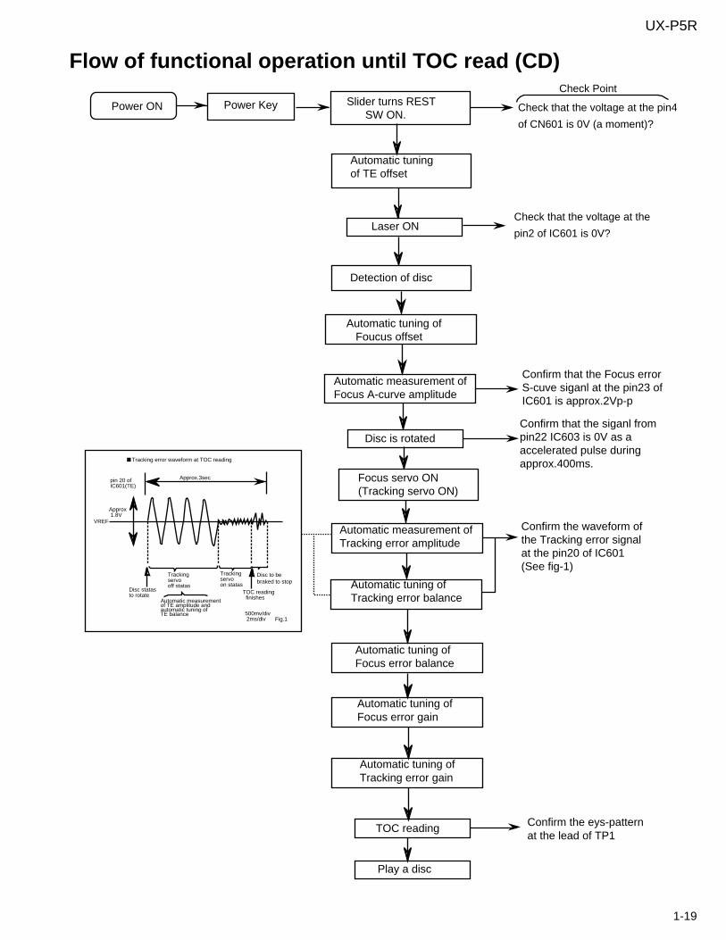
Flow of functional operation until TOC read (CD)
Slider turns REST SW ON.
Automatic tuningof TE offset
Laser ON
Detection of disc
Automatic measurement ofFocus A-curve amplitude
Automatic tuning of Foucus offset
Disc is rotated
Focus servo ON(Tracking servo ON)
Automatic tuning ofTracking error balance
Automatic measurement ofTracking error amplitude
Automatic tuning ofFocus error balance
Disc to bebraked to stop
Trackingservoon statas
Trackingservooff statas
Disc statasto rotate TOC reading
finishesAutomatic measurementof TE amplitude and automatic tuning ofTE balance 500mv/div
2ms/div Fig.1
Approx.3secpin 20 ofIC601(TE)
Approx 1.8V
VREF
Tracking error waveform at TOC reading
Power ON Power Key
Confirm that the Focus errorS-cuve siganl at the pin23 ofIC601 is approx.2Vp-p
Confirm that the siganl frompin22 IC603 is 0V as a accelerated pulse during approx.400ms.
Confirm the waveform ofthe Tracking error signalat the pin20 of IC601(See fig-1)
Automatic tuning ofFocus error gain
Automatic tuning ofTracking error gain
TOC reading
Play a disc
Confirm the eys-patternat the lead of TP1
Check that the voltage at the pin4
of CN601 is 0V (a moment)?
Check Point
Check that the voltage at the
pin2 of IC601 is 0V?
1-20
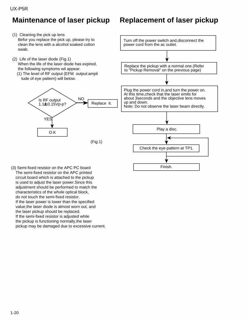
UX-P5R
Turn off the power switch and,disconnect thepower cord from the ac outlet.
Replace the pickup with a normal one.(Refer to "Pickup Removal" on the previous page)
Plug the power cord in,and turn the power on.At this time,check that the laser emits for about 3seconds and the objective lens moves up and down.Note: Do not observe the laser beam directly.
Play a disc.
Check the eye-pattern at TP1.
Finish.
Maintenance of laser pickup
(1) Cleaning the pick up lens Befor you replace the pick up, please try to clean the lens with a alcohol soaked cotton swab.
(2) Life of the laser diode (Fig.1) When the life of the laser diode has expired, the following symptoms wil appear. (1) The level of RF output (EFM output:ampli tude of eye pattern) will below.
Is RF output1.1 0.15Vp-p? Replace it.
NO
YES
O.K
(3) Semi-fixed resistor on the APC PC board The semi-fixed resistor on the APC printed circuit board which is attached to the pickup is used to adjust the laser power.Since this adjustment should be performed to match the characteristics of the whole optical block, do not touch the semi-fixed resistor. If the laser power is lower than the specified value,the laser diode is almost worn out, and the laser pickup should be replaced. If the semi-fixed resistor is adjusted while the pickup is functioning normally,the laser pickup may be damaged due to excessive current.
(Fig.1)
Replacement of laser pickup
1-21
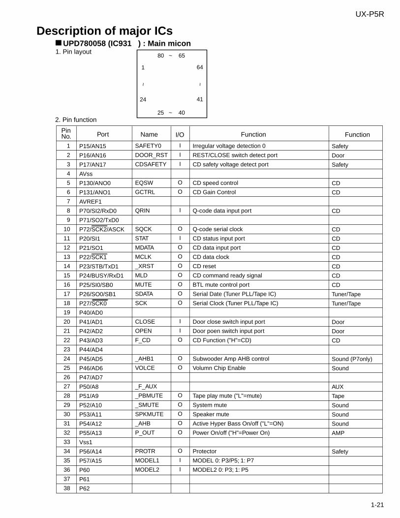
UX-P5R
1. Pin layout80 ~ 65
25 ~ 40
1
24
~
64
41
~
2. Pin function
UPD780058 (IC931 ) : Main micon
PinNo. Port Name I/O Function Function
1
2
3
4
5
6
7
8
9
10
11
12
13
14
15
16
17
18
19
20
21
22
23
24
25
26
27
28
29
30
31
32
33
34
35
36
37
38
P15/AN15
P16/AN16
P17/AN17
AVss
P130/ANO0
P131/ANO1
AVREF1
P70/SI2/RxD0
P71/SO2/TxD0
P72/SCK2/ASCK
P20/SI1
P21/SO1
P22/SCK1
P23/STB/TxD1
P24/BUSY/RxD1
P25/SI0/SB0
P26/SO0/SB1
P27/SCK0
P40/AD0
P41/AD1
P42/AD2
P43/AD3
P44/AD4
P45/AD5
P46/AD6
P47/AD7
P50/A8
P51/A9
P52/A10
P53/A11
P54/A12
P55/A13
Vss1
P56/A14
P57/A15
P60
P61
P62
SAFETY0
DOOR_RST
CDSAFETY
EQSW
GCTRL
QRIN
SQCK
STAT
MDATA
MCLK
_XRST
MLD
MUTE
SDATA
SCK
CLOSE
OPEN
F_CD
_AHB1
VOLCE
_F_AUX
_PBMUTE
_SMUTE
SPKMUTE
_AHB
P_OUT
PROTR
MODEL1
MODEL2
I
I
I
O
O
I
O
I
O
O
O
O
O
O
O
I
I
O
O
O
O
O
O
O
O
O
I
I
Irregular voltage detection 0
REST/CLOSE switch detect port
CD safety voltage detect port
CD speed control
CD Gain Control
Q-code data input port
Q-code serial clock
CD status input port
CD data input port
CD data clock
CD reset
CD command ready signal
BTL mute control port
Serial Date (Tuner PLL/Tape IC)
Serial Clock (Tuner PLL/Tape IC)
Door close switch input port
Door poen switch input port
CD Function ("H"=CD)
Subwooder Amp AHB control
Volumn Chip Enable
Tape play mute ("L"=mute)
System mute
Speaker mute
Active Hyper Bass On/off ("L"=ON)
Power On/off ("H"=Power On)
Protector
MODEL 0: P3/P5; 1: P7
MODEL2 0: P3; 1: P5
Safety
Door
Safety
CD
CD
CD
CD
CD
CD
CD
CD
CD
CD
Tuner/Tape
Tuner/Tape
Door
Door
CD
Sound (P7only)
Sound
AUX
Tape
Sound
Sound
Sound
AMP
Safety
Description of major ICs
1-22
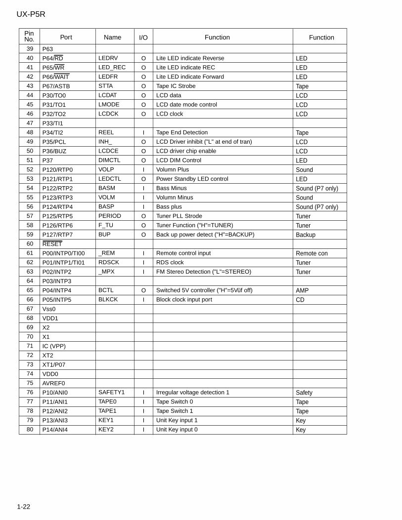
UX-P5R
PinNo. Port Name I/O Function Function
39
40
41
42
43
44
45
46
47
48
49
50
51
52
53
54
55
56
57
58
59
60
61
62
63
64
65
66
67
68
69
70
71
72
73
74
75
76
77
78
79
80
P63
P64/RD
P65/WR
P66/WAIT
P67/ASTB
P30/TO0
P31/TO1
P32/TO2
P33/TI1
P34/TI2
P35/PCL
P36/BUZ
P37
P120/RTP0
P121/RTP1
P122/RTP2
P123/RTP3
P124/RTP4
P125/RTP5
P126/RTP6
P127/RTP7
RESET
P00/INTP0/TI00
P01/INTP1/TI01
P02/INTP2
P03/INTP3
P04/INTP4
P05/INTP5
Vss0
VDD1
X2
X1
IC (VPP)
XT2
XT1/P07
VDD0
AVREF0
P10/ANI0
P11/ANI1
P12/ANI2
P13/ANI3
P14/ANI4
LEDRV
LED_REC
LEDFR
STTA
LCDAT
LMODE
LCDCK
REEL
INH_
LCDCE
DIMCTL
VOLP
LEDCTL
BASM
VOLM
BASP
PERIOD
F_TU
BUP
_REM
RDSCK
_MPX
BCTL
BLKCK
SAFETY1
TAPE0
TAPE1
KEY1
KEY2
O
O
O
O
O
O
O
I
O
O
O
I
O
I
I
I
O
O
O
I
I
I
O
I
I
I
I
I
I
Lite LED indicate Reverse
Lite LED indicate REC
Lite LED indicate Forward
Tape IC Strobe
LCD data
LCD date mode control
LCD clock
Tape End Detection
LCD Driver inhibit ("L" at end of tran)
LCD driver chip enable
LCD DIM Control
Volumn Plus
Power Standby LED control
Bass Minus
Volumn Minus
Bass plus
Tuner PLL Strode
Tuner Function ("H"=TUNER)
Back up power detect ("H"=BACKUP)
Remote control input
RDS clock
FM Stereo Detection ("L"=STEREO)
Switched 5V controller ("H"=5Vuf off)
Block clock input port
Irregular voltage detection 1
Tape Switch 0
Tape Switch 1
Unit Key input 1
Unit Key input 0
LEDLEDLEDTapeLCDLCDLCD
TapeLCDLCDLEDSoundLEDSound (P7 only)SoundSound (P7 only)TunerTunerBackup
Remote conTunerTuner
AMPCD
SafetyTapeTapeKeyKey
1-23
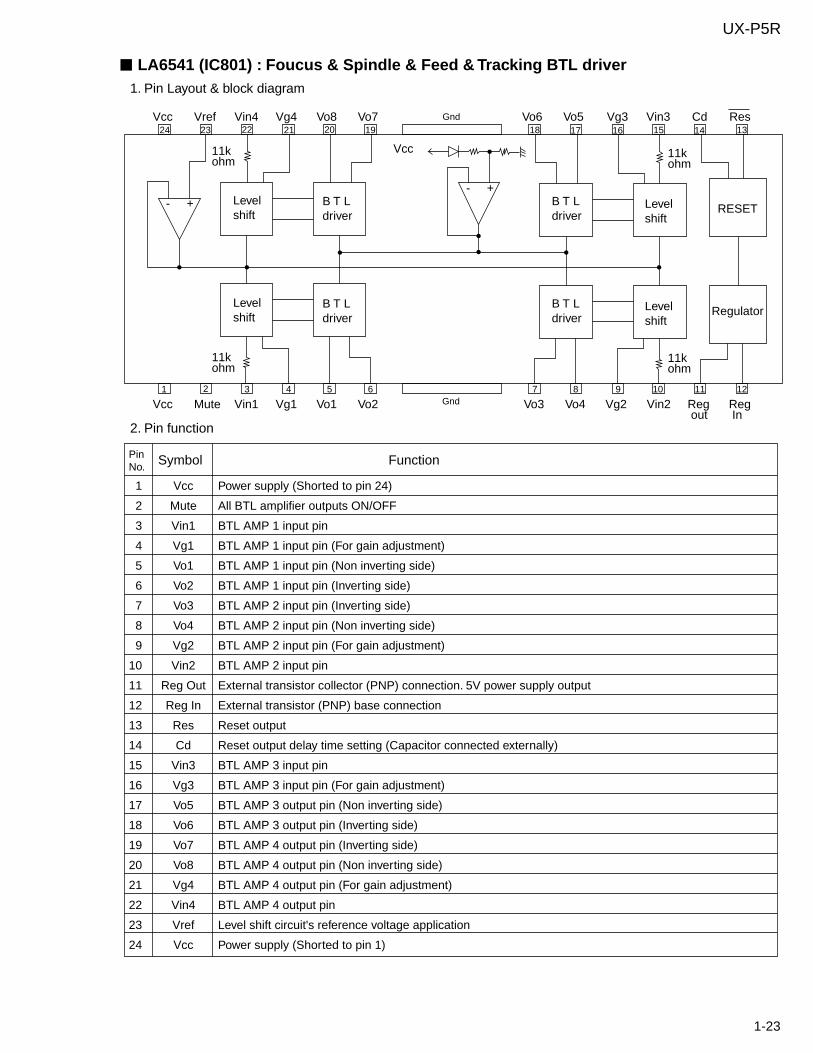
UX-P5R
24 23 22 21 20 19Gnd
18 17 16 15 14 13
7 8 9 10 11 12Gnd
1 2 3 4 5 6
Levelshift
B T Ldriver
Levelshift
B T Ldriver
B T Ldriver
11kohm
11kohm
Levelshift
B T Ldriver
Levelshift
Regulator
RESET
11kohm
11kohm
- +- +
Vcc
Vcc Vref Vin4 Vg4 Vo8 Vo7
Vcc Mute Vin1 Vg1 Vo1 Vo2 Vo3 Vo4 Vg2 Vin2 Reg out
Reg In
Vo6 Vo5 Vg3 Vin3 Cd Res
LA6541 (IC801) : Foucus & Spindle & Feed & Tracking BTL driver1. Pin Layout & block diagram
2. Pin function
1
2
3
4
5
6
7
8
9
10
11
12
13
14
15
16
17
18
19
20
21
22
23
24
Vcc
Mute
Vin1
Vg1
Vo1
Vo2
Vo3
Vo4
Vg2
Vin2
Reg Out
Reg In
Res
Cd
Vin3
Vg3
Vo5
Vo6
Vo7
Vo8
Vg4
Vin4
Vref
Vcc
Power supply (Shorted to pin 24)
All BTL amplifier outputs ON/OFF
BTL AMP 1 input pin
BTL AMP 1 input pin (For gain adjustment)
BTL AMP 1 input pin (Non inverting side)
BTL AMP 1 input pin (Inverting side)
BTL AMP 2 input pin (Inverting side)
BTL AMP 2 input pin (Non inverting side)
BTL AMP 2 input pin (For gain adjustment)
BTL AMP 2 input pin
External transistor collector (PNP) connection. 5V power supply output
External transistor (PNP) base connection
Reset output
Reset output delay time setting (Capacitor connected externally)
BTL AMP 3 input pin
BTL AMP 3 input pin (For gain adjustment)
BTL AMP 3 output pin (Non inverting side)
BTL AMP 3 output pin (Inverting side)
BTL AMP 4 output pin (Inverting side)
BTL AMP 4 output pin (Non inverting side)
BTL AMP 4 output pin (For gain adjustment)
BTL AMP 4 output pin
Level shift circuit's reference voltage application
Power supply (Shorted to pin 1)
PinNo. Symbol Function
1-24
UX-P5R
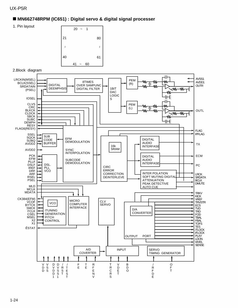
MN662748RPM (IC651) : Digital servo & digital signal processer
1. Pin layout20 ~ 1
41 ~ 60
21
40
~
80
61
~
2.Block diagram
OFT
/RFDE
BDO
VDET
TRCRS
RFENV
TE
FE
INPUT SERVOTIMING GENERATOR
A/DCOVERTER
/TEST
/RST
DVSS1
DVDD1
VSS
VDD
CLVSERVO
MICROCOMPUTERINTERFACE
VCO
ITUNINGGENERATIONPITCHCONTROL
ÊSTAT
CK384(EFM) VCOF BYTCK SMCK FCLK CSEL MSEL X2 X1
PCK EFMPLLFDSLF IREF DRF ARFRSELPSEL
MLD MCLKMDATA
DSL.PLLVCO
AVDD2
SUBCODEBUFFER
SSEL SQCK SUBQAVDD2
CLVS CRC
BLKCKCLDCK SBCK SUBC
DEMPH RESY
FLAG6(RESY)
EFMDEMODULATION
SUBCODEDEMODULATION
SYNCINTERPOLATION
16kSRAM
CIRCERRORCORRECTIONDEINTERLEVE
LRCKIN(MSEL) BCLK(SSEL) SRDATAIN (PSEL)
IOSEL
DIGITALDEEMPHSIS
8TIMESOVER SAMPUNCDIGITAL FILTER 1BIT
DACLOGICS
PEM(R)
PEM(L)
DIGITALAUDIOINTERFASE
DIGITALAUDIOINTERFASE
INTER POLATIONSOFT MUTING DIGITALATTENUATIONPEAK DETECTIVEAUTO CUE
D/ACONVERTER
OUTPUT PORT
AVSS1AVDD1OUTR
OUTL
FLAGIPFLAG
TX
ECM
PC
LRCKSRDATABCLKDMUTE
TRKVKICKVREFTRVSTRECSTVDTRDFODTBALFBALTOFSTES/TLOCK/FLOCKPLAYLDONWVELSENSE
1-25
UX-P5R
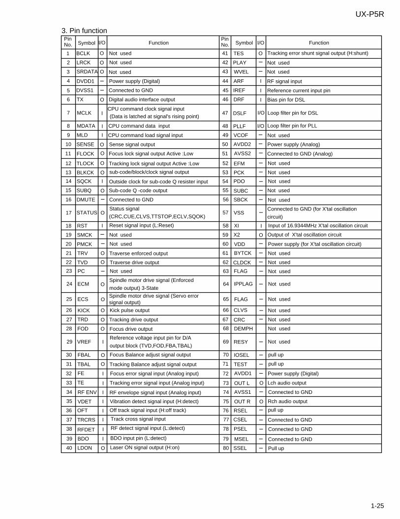
3. Pin functionPinNo. Symbol I/O
O
O
O
1
2
3
4
5
6
7
8
9
10
11
12
13
14
15
16
17
18
19
20
21
22
23
24
25
26
27
28
29
30
31
32
33
34
35
36
37
38
39
40
PinNo. Symbol I/O
42
41
43
44
45
46
47
48
49
50
51
52
53
54
55
56
57
58
59
60
61
62
63
64
65
66
67
68
69
70
71
72
73
74
75
76
77
78
79
80
O
II
II
O
BCLK
LRCK
SRDATA
DVDD1
DVSS1
TX
MCLK
MDATA
MLD
I
I
I
SENSE
FLOCK
TLOCK
BLKCK
SQCK
O
O
O
O
O
O
I
II
I
I
SUBQ
DMUTE
STATUS
I
O
O
RST
SMCK
PMCK
TRV
TVD
PC
ECM
ECS
KICK
TRD
O
O
O
O
O
O
O
I
I
I
FOD
VREF
FBAL
TBAL
FE
TE
I
I
I
I
IRF ENV
VDET
OFT
TRCRS
I
O
RFDET
BDO
LDON
Function
Not used
Not used
Not used
Connected to GND
Digital audio interface output
Power supply (Digital)
CPU command clock signal input
CPU command load signal input
CPU command data input
Focus lock signal output Active :Low
Sense signal output
(Data is latched at signal's rising point)
Tracking lock signal output Active :Low
sub-code/block/clock signal output
Outside clock for sub-code Q resister input
Sub-code Q -code output
Connected to GND
Status signal
(CRC,CUE,CLVS,TTSTOP,ECLV,SQOK)
Reset signal input (L:Reset)
Not used
Not used
Traverse enforced output
Traverse drive output
Not used
Spindle motor drive signal (Enforced
mode output) 3-State
Spindle motor drive signal (Servo errorsignal output)
Kick pulse output
Tracking drive output
Focus drive output
Reference voltage input pin for D/A
output block (TVD,FOD,FBA,TBAL)
Focus Balance adjust signal output
Tracking Balance adjust signal output
Focus error signal input (Analog input)
Tracking error signal input (Analog input)
RF envelope signal input (Analog input)
Vibration detect signal input (H:detect)
Off track signal input (H:off track)
Track cross signal input
RF detect signal input (L:detect)
BDO input pin (L:detect)
Laser ON signal output (H:on)
I
I
I
I/O
I/O
II
II
II
Function
Not used
Not used
TES
PLAY
WVEL
ARF
IREF
DRF
DSLF
PLLF
Tracking error shunt signal output (H:shunt)
RF signal input
Reference current input pin
Bias pin for DSL
Not used
Loop filter pin for DSL
Loop filter pin for PLL
Power supply (Analog)
Connected to GND (Analog)
Not used
Not used
Not used
Not used
Not used
II
II
Connected to GND (for X'tal oscillation
circuit)
I
O
I
O
O
II
II
II
II
II
II
II
II
Not used
Not used
Not used
Not used
Not used
Not used
Not used
Not used
Not used
Pull up
Connected to GND
Connected to GND
Connected to GND
pull up
pull up
pull up
Power supply (Digital)
Lch audio output
Connected to GND
Rch audio output
Power supply (for X'tal oscillation circuit)
Input of 16.9344MHz X'tal oscillation circuit
Output of X'tal oscillation circuit
VCOF
AVDD2
AVSS2
EFM
PCK
PDO
SUBC
SBCK
VSS
XI
X2
VDD
BYTCK
CLDCK
FLAG
IPPLAG
FLAG
CLVS
CRC
DEMPH
RESY
IOSEL
TEST
AVDD1
OUT L
AVSS1
OUT R
RSEL
SSEL
MSEL
PSEL
CSEL
1-26
UX-P5R
1
2
8 Vcc
7 OUT2
6 -IN2
5 +IN2
OUT1 1
-IN1 2
+IN1 3
VEE 4
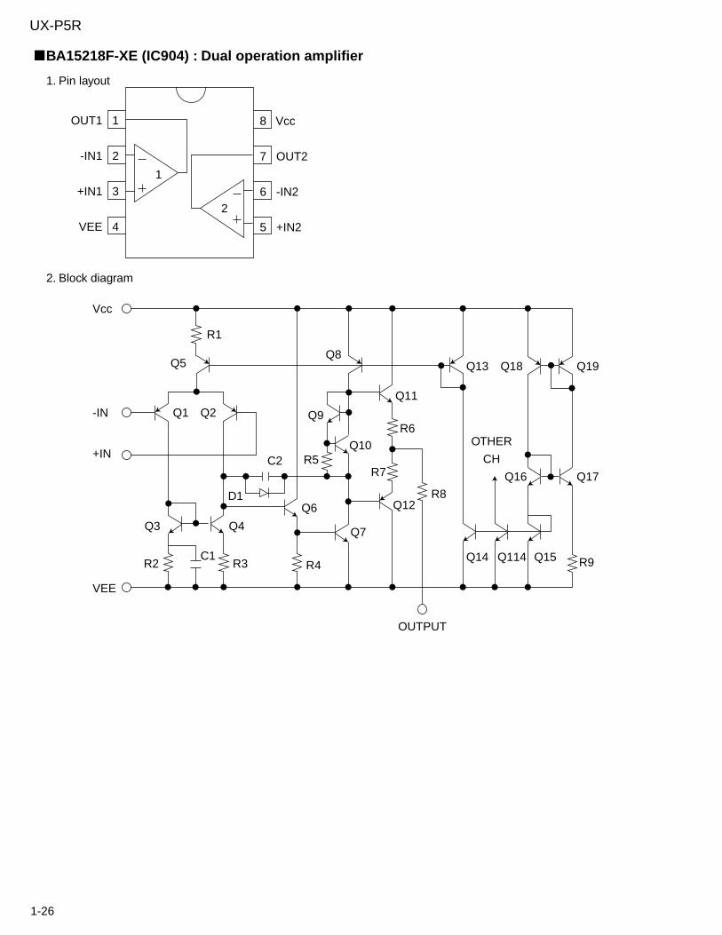
BA15218F-XE (IC904) : Dual operation amplifier
1. Pin layout
2. Block diagram
Q19
Q17Q16
OTHER
CH
R9
R6
R8
R7R5
R4R3R2
R1
D1
C1
Q18Q13
Q11
Q8Q5
Vcc
VEE
OUTPUT
-IN
+IN
Q1
Q3 Q4
Q2
C2
Q9
Q6
Q7
Q10
Q12
Q14 Q15Q114
1-27
UX-P5R
Q14
Q12
Q13
Q10
Q11Q4
Q3 Q5
Q6
Q1
Q2 Q7 Q8
Q9
Z1
R9
R3
R4
R1
R2
R8
R7
R5
R6
Q16
R11
R10
C1
3 INPUT
1 OUTPUT
2 COMMON
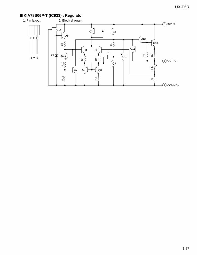
KIA78S06P-T (IC933) : Regulator1. Pin layout 2. Block diagram
1 2 3
1-28
UX-P5R
15
14
13
12
11
10
9
8
7
6
5
4
3
2
1
1. Pin layout
2. Block diagram
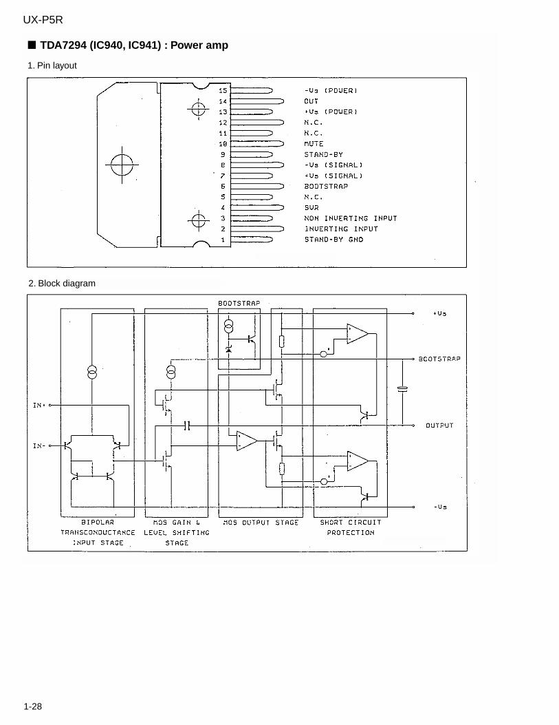
TDA7294 (IC940, IC941) : Power amp
1-29
UX-P5R
1. Pin layout
1
2
3
4
5
6
7
8
9
10
11
12
13
14
15
PD
LD
VCC
RFN
RF OUT
RF IN
C.AGC
ARF
CEA
3TOUT
CBDO
BDO
COFTR
OFTR
NRFDET
APC Amp. Input terminal
APC Amp.Output terminal
Power supply terminal
RF addition Amp.Reversing input terminal
RF addition Amp.Output terminal
AGC input terminal
Terminal of connection of capacity of AGC loop
filter.
AGC output terminal
Capacity connection terminal for HPF-Amp.
3TENV output terminal
Capacity connection terminal for RF shade side
envelope detection
BDO output terminal
Capacity connection terminal for RF discernment
side envelope detection
OFTR output terminal
NRFDET output terminal
16
17
18
19
20
21
22
23
24
25
26
27
28
29
30
31
32
CDDG
VREF
VDET
TEBPF
TEOUT
TEN
FEN
FEOUT
GCTL
FBAL
TBAL
E
F
D
B
C
A
Earth terminal
VREF output terminal
VDET output terminal
VDET input terminal
TE Amp. output terminal
TE Amp. reversing input terminal
FE Amp. reversing input terminal
FE Amp. output terminal
Terminal GCTL & APC
FBAL control terminal
TBAL control terminal
Tracking signal input terminal 1
Tracking signal input terminal 2
Focus signal input terminal 4
Focus signal input terminal 2
Focus signal input terminal 3
Focus signal input terminal 1
2. Block
3. Function
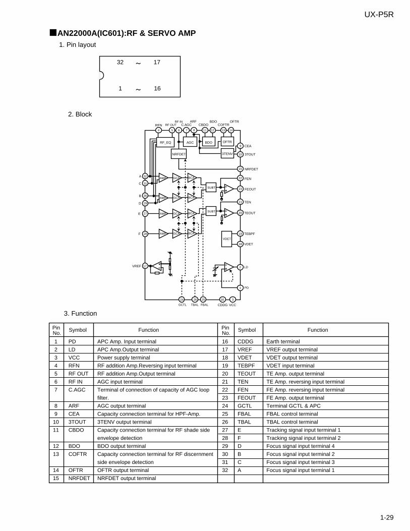
AN22000A(IC601):RF & SERVO AMP
Pin No.
Symbol Function Pin No.
Symbol Function
A
C
B
D
E
F
VREF
CDDG VCC
VDET
TEBPF
TEOUT
TEN
FEOUT
NRFDET
3TOUT
CEA
OFTRCOFTR
BDOCBDO
ARFC.AGCRFN
FEN
RF_EQ AGC BDO OFTR
3TENVNRFDET
AMP GCA BCA
AMP GCA BCA
AMP GCA BCA
AMP GCA BCA
RF OUTRF IN
SUBT
SUBT
GCTL TBAL FBAL
24 26 25 16 3
1
2
18
19
20
21
23
22
15
10
1413121187654
9
32
31
30
29
27
28
17
PD
LD
VDET
32 17
1 16
1-30
UX-P5R
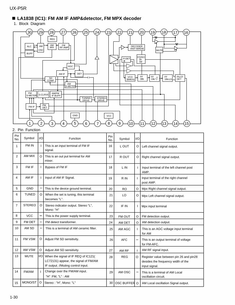
2. Pin Function
PinNo. Symbol I/O Function FunctionI/OSymbol
PinNo.
1
2
3
4
5
6
7
8
9
10
11
12
13
14
15
FM IN
AM MIX
FM IF
AM IF
GND
TUNED
STEREO
VCC
FM DET
AM SD
FM VSM
AM VSM
MUTE
FM/AM
MONO/ST O
I
I/O
O
O
I
O
I
I
I
O
O
IIII
I
This is an input terminal of FM IFsignal.
This is an out put terminal for AMmixer.
Bypass of FM IF
Input of AM IF Signal.
This is the device ground terminal.
When the set is tuning, this terminal
becomes "L".
Stereo indicator output. Stereo "L",Mono: "H"
This is the power supply terminal.
FM detect transformer.
This is a terminal of AM ceramic filter.
Adjust FM SD sensitivity.
Adjust AM SD sensitivity.
When the signal of IF REQ of IC121(
LC72131) appear, the signal of FM/AM
IF output. //Muting control input.
Change over the FM/AM input.
"H" :FM, "L" : AM
Stereo : "H", Mono: "L"
16
17
18
19
20
21
22
23
24
25
26
27
28
29
30 OSC BUFFER
AM OSC
REG
AM RF
AFC
AM AGC
O
I
O
I
I
I
AM Local oscillation Signal output.
This is a terminal of AM Localoscillation circuit.
Register value between pin 26 and pin28
desides the frequency width of the
input signal.
AM RF signal input.
This is an output terminal of voltage
for FM-AFC.
This is an AGC voltage input terminal
for AM
O
O
I
O
AM detection output.
FM detection output.
Mpx input terminal
O
O
I
Left channel signal output.
Right channel signal output.
Input terminal of the left channel post
AMP.
Input terminal of the right channel
post AMP.I
O
Mpx Left channel signal output.
Mpx Right channel signal output.
L OUT
R OUT
L IN
R IN
RO
LO
IF IN
FM OUT
AM DET
1. Block Diagram
ALC
BUFF
AM
OSC
REG
AMMIX
FMRF.AMP
AGC
AM IF DET
SDCOMP
AMS-METER
FMS-METER
FM IFPMDET
S-CLRVEAM/FMIF-BUFF
TUNING DRIVE
GND VCC
STEREO DRIVE
MUTE
DECODERANIT-BIRDIE
STEREO 5N SW
P-DET
PILOTDET
FF19k
FF19k
FF38k
VCO384KHz / 2 /LS
30 29 28 27 26 25 24 23 22 21 20 19 18 17 16
1 2 3 4 6 7 8 9 10 11 12 13 14 155
LA1838 (IC1): FM AM IF AMP&detector, FM MPX decoder
1-31
UX-P5R
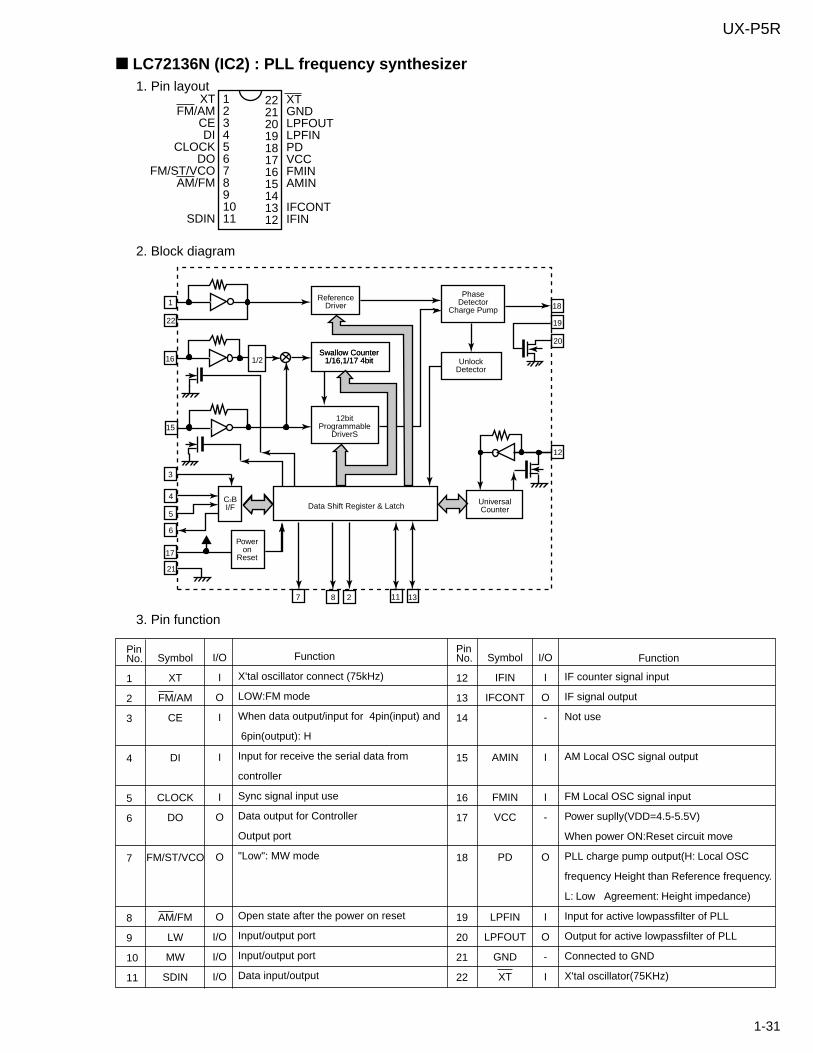
1. Pin layout1234567891011
2221201918171615141312
XTFM/AM
CEDI
CLOCKDO
FM/ST/VCOAM/FM
SDIN
XTGNDLPFOUTLPFINPDVCCFMINAMIN
IFCONTIFIN
PinNo.
1
2
3
4
5
6
7
8
9
10
11
PinNo.
12
13
14
15
16
17
18
19
20
21
22
Symbol
XT
FM/AM
CE
DI
CLOCK
DO
FM/ST/VCO
AM/FM
LW
MW
SDIN
Symbol
IFIN
IFCONT
AMIN
FMIN
VCC
PD
LPFIN
LPFOUT
GND
XT
Function
X'tal oscillator connect (75kHz)
LOW:FM mode
When data output/input for 4pin(input) and
6pin(output): H
Input for receive the serial data from
controller
Sync signal input use
Data output for Controller
Output port
"Low": MW mode
Open state after the power on reset
Input/output port
Input/output port
Data input/output
Function
IF counter signal input
IF signal output
Not use
AM Local OSC signal output
FM Local OSC signal input
Power suplly(VDD=4.5-5.5V)
When power ON:Reset circuit move
PLL charge pump output(H: Local OSC
frequency Height than Reference frequency.
L: Low Agreement: Height impedance)
Input for active lowpassfilter of PLL
Output for active lowpassfilter of PLL
Connected to GND
X'tal oscillator(75KHz)
I/O
I
O
I
I
I
O
O
O
I/O
I/O
I/O
I/O
I
O
-
I
I
-
O
I
O
-
I
ReferenceDriver
PhaseDetector
Charge Pump
UnlockDetector
UniversalCounter
Swallow Counter1/16,1/17 4bit
12bitProgrammable
DriverS
Swallow Counter1/16,1/17 4bit
Data Shift Register & Latch
Poweron
Reset
C2BI/F
1/2
7 8 2 11 13
21
17
6
5
4
3
15
16
22
1 18
19
20
12
2. Block diagram
3. Pin function
LC72136N (IC2) : PLL frequency synthesizer
1-32
UX-P5R
Pin Assignment
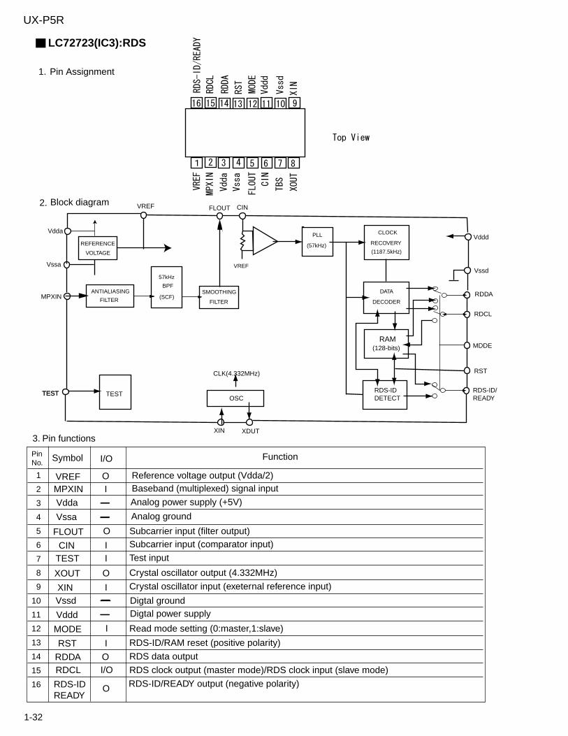
LC72723(IC3):RDS
Block diagram
Vdda
Vssa
MPXIN
TEST
VREF FLOUT CIN
Vddd
Vssd
RDDA
RDCL
MDDE
RST
RDS-ID/READY
XDUTXIN
REFERENCE
VOLTAGE
ANTIALIASING
FILTER
57kHz
BPF
(SCF)
VREF
SMOOTHING
FILTER
PLL
(57kHz)
CLOCK
RECOVERY
(1187.5kHz)
DATA
DECODER
RAM(128-bits)
RDS-IDDETECT
CLK(4.332MHz)
OSCTEST
1.
2.
3. Pin functions
1
2
3
4
5
6
7
8
9
10
11
12
13
14
15
16
PinNo. Symbol Function
VREFMPXIN
Vdda
Vssa
FLOUT
CINTEST
XOUT
XINVssd
Vddd
MODE
RST
RDDARDCL
RDS-IDREADY
I/O
O
O
O
O
O
I
I
I
I
I
I
I/O
Reference voltage output (Vdda/2)Baseband (multiplexed) signal input
Analog power supply (+5V)
Analog ground
Subcarrier input (comparator input)Subcarrier input (filter output)
Test input
Crystal oscillator input (exeternal reference input)
Crystal oscillator output (4.332MHz)
Digtal groundDigtal power supply
Read mode setting (0:master,1:slave)
RDS-ID/RAM reset (positive polarity)
RDS data output
RDS clock output (master mode)/RDS clock input (slave mode)
RDS-ID/READY output (negative polarity)
1-33
UX-P5R
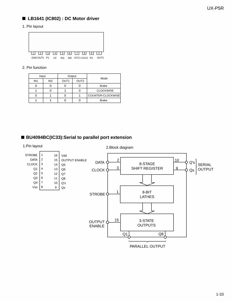
1 2 3 4 5 6 7 8 9 10
GND OUT1 P1 VZ IN1 IN2 VCC1 VCC2 P2 OUT2
Input OutputMode
IN1 IN2 OUT1 OUT2
Brake0 0 0 0
1 0 1 0
0 1 0 1
1 1 0 0
CLOCKWISE
COUNTER-CLOCKWISE
Brake
LB1641 (IC802) : DC Motor driver
1. Pin layout
2. Pin function
STROBE
DATA
CLOCK
Q1
Q2
Q3
Q4
Vss
Vdd
OUTPUT ENABLE
Q5
Q6
Q7
Q8
Q's
Qs
1
2
3
4
5
6
7
8
16
15
14
13
12
11
10
9
1.Pin layout
8-STAGESHIFT REGISTER
8-BITLATHES
3-STATEOUTPUTS
1
2
3
15
Q1 Q8
10
9
DATA
CLOCK
STROBE
OUTPUTENABLE
PARALLEL OUTPUT
Q's
QsSERIALOUTPUT
2.Block diagram
BU4094BC(IC33):Serial to parallel port extension
1-34
UX-P5R
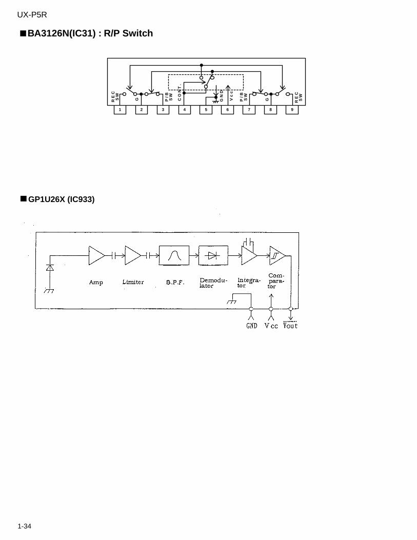
GP1U26X (IC933)
BA3126N(IC31) : R/P Switch
R E
CS
W
G
1 2 3 4 5 6 7 8 9
P /
BS
W
P /
BS
W
G R E
CS
W
C O
N T
.
G N
D
V c
c
1-35
UX-P5R
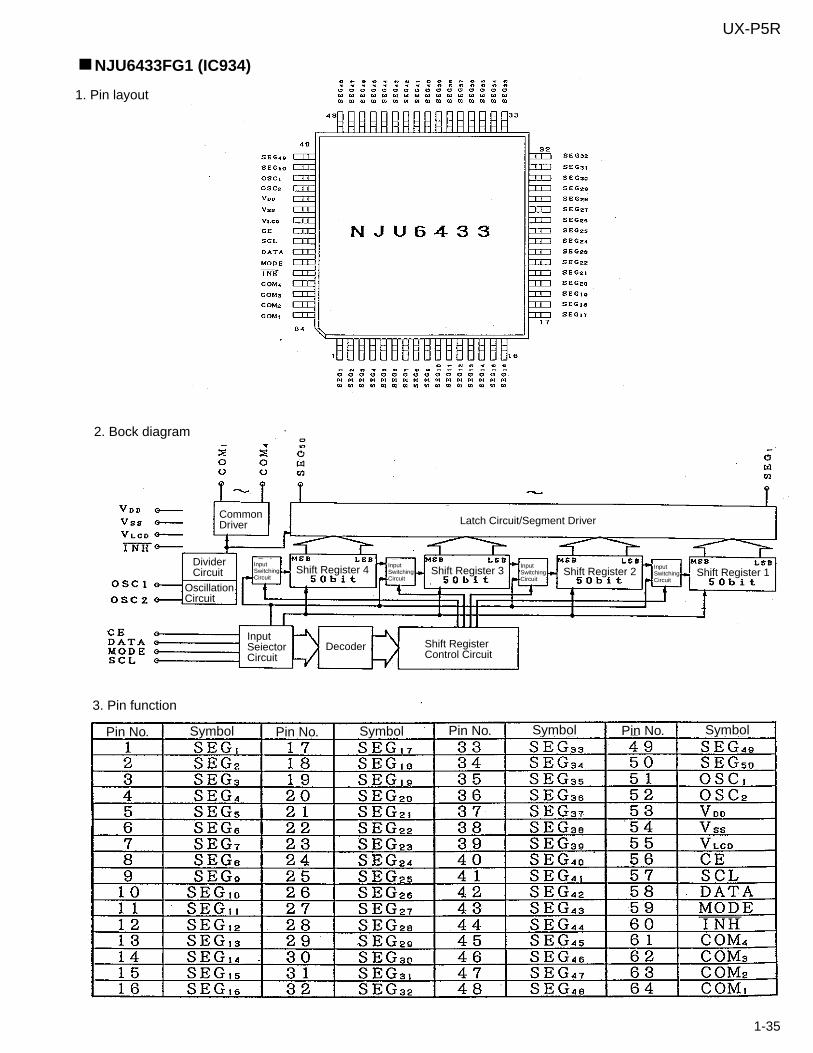
NJU6433FG1 (IC934)
1. Pin layout
Common Driver Latch Circuit/Segment Driver
Divider Circuit
Oscillation Circuit
Input Switching Circuit
Shift Register 4 Input Switching Circuit
Input Switching Circuit
Input Switching Circuit
Shift Register 3 Shift Register 2 Shift Register 1
Input Seiector Circuit
Decoder Shift Register Control Circuit
2. Bock diagram
Pin No. Symbol Pin No. Symbol Pin No. Symbol Pin No. Symbol
3. Pin function
1-36
UX-P5R
1. Pin layout
LC75345M (IC901)
2. Block Diagram
1-37
UX-P5R
3. Descriptions
1-38
UX-P5R
1-39
UX-P5R
AN7317 (IC32) : PB/REC amp
1-40
UX-P5R
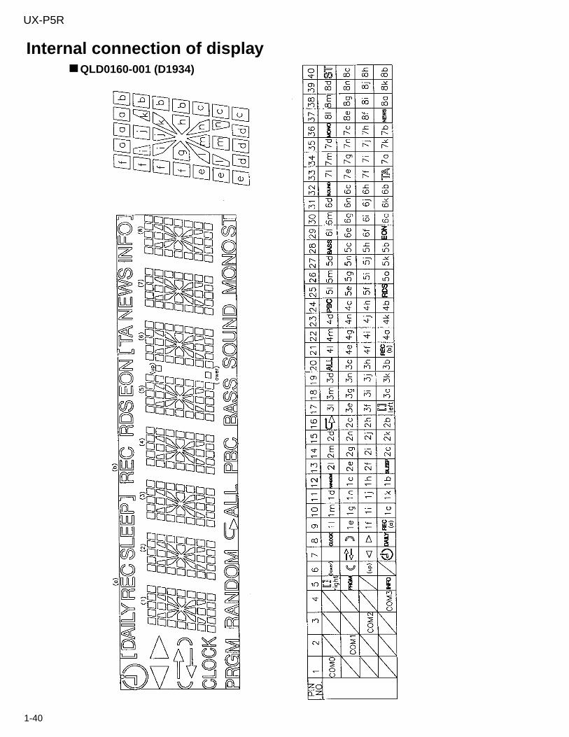
QLD0160-001 (D1934)
Internal connection of display
1-41
UX-P5R
Printed in Japan200103(O) No.20917
UX-P5R
VICTOR COMPANY OF JAPAN, LIMITEDAUDIO & COMMUNICATION BUSINESS DIVISIONPERSONAL & MOBILE NETWORK BUSINESS UNIT 10-1,1Chome,Ohwatari-machi,Maebashi-city,371-8543,Japan
2-1
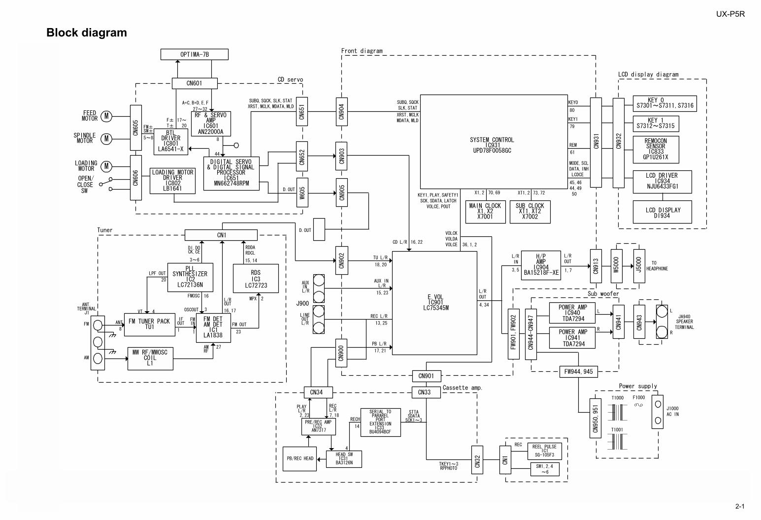
UX-P5R
IHA B C D E F G
1
2
3
4
5
6
Block diagram
2-2
IHA B C D E F G
1
2
3
4
5
6
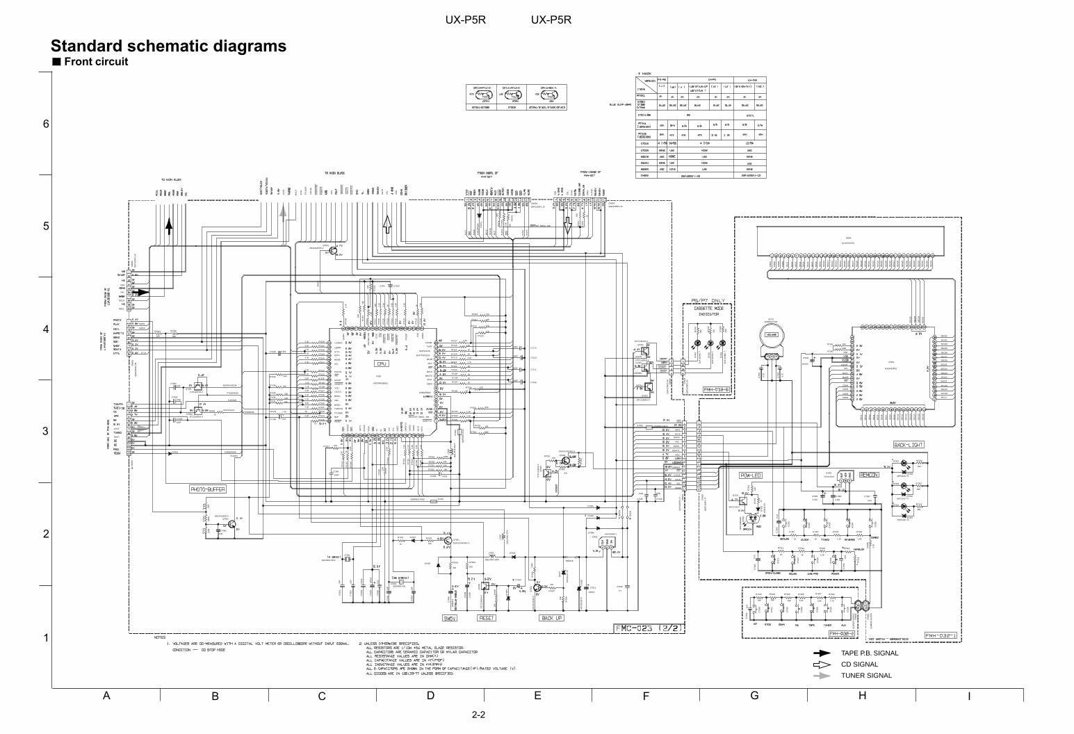
UX-P5R UX-P5R
Front circuitStandard schematic diagrams
TAPE P.B. SIGNAL
CD SIGNAL
TUNER SIGNAL
IC934
IC931
R7103
R7342
R7341
JS731
R7252
R7203
K7001
R7064
D7005
R7217
R7218
R7128
R7129
R7130
R7065
R7131
D7009
C7144
R7137
R7308R7309
R7139
R7140
R7141
R7142
L7001
C7136
Q7061
Q7062R7144
IC932
C7012
R7232
B2018
C7341
C7135
R7115
R7114
R7111
R7107
C7011
R7106
R7117
R7116
D7006
D7004
R7002
R7316
R7102
R7101
R7007
C7010
R7214
D7002 R7003 R7004
Q7041
Q7001D7001R7001
R7215
X7001
X7002
R7202
R7062
R7132
R7133
D7363
R7307
IC933
C7301 C7302
K7003
Q7331
C7062
C7061
R7092
R7313R7312R7311
C7063
R7314
R7201
CN903
C7115
C7113
C7111
R7134
C7128
R7240
R7239
R7145
R7110
R7238
R7236
R7143
DI934
R7255
R7247
R7301 R7302 R7303 R7304
R7306
D7362
C7149
Q7092
R7254
R7323
R7322
D7323
D7322
D7321
D7061
R7091
R7206
R7135
CN904
C7152
R7321
D7361
C7041
C7307
Q7031
C7123
R7310
R7136
R7109
R7253
R7108
C7108
R7138
R7113
R7112
Q7401
Q7402
Q7403
R7160
R7159
R70
76
S73
09
K70
02
Q70
02
S73
10
R71
25
R71
26
R71
27
L700
3
R71
24
R71
23
R71
22
R71
21
R71
20R71
57
S73
07
C73
16
R71
52
R71
51
D70
07
R70
08
Q70
03
R71
47
R70
06
D70
03
R70
05
D70
08
C70
05
C70
06
C70
07
C70
04
R71
48
L700
2
C70
02
C70
01
Q70
91
R70
43
R70
93R
7077
R71
50
R70
78
R71
53
R71
55
C73
03
S73
08
C70
08
R71
49
S73
12
R71
46
R73
31
R71
54
S73
13
S73
14
S73
15
R71
18
R71
19
B23
23
B22
21
S73
01
S73
02
S73
03
S73
05
S73
04
S73
06
R73
05
R73
15
R72
21
C70
09
R70
75
R70
42R
7041
D73
32
D73
31
R73
32
CN
933
CN
934
C73
06
C73
05
C73
04
CN
901
S73
11
C73
52
C73
51
D70
71
C70
03
CN
900
CN
902
R70
79
FW
931
CN
931
CN
932
D74
01
D74
02
D74
03
R74
02
R74
03
R74
01
FW
931
R71
58
LEDRV
REM
DIMMER
INH
RST
SCD
REST/OP_SW/CL_SW
SAFETY0
INH
REST/OP_SW/CL_SW
LEDREC
LEDFR
RESET
INH
DIM
ME
R
RS
T
MP
X
SP
KM
UT
E
AH
B
SP
KM
UT
E
SM
UT
E
PB
MU
TE
LIN
EM
UT
E
PB
MU
TE
RE
M
SC
D
SM
UT
E
LIN
EM
UT
E
SA
FE
TY
0
NJU6433FG1
UPD78F0058GC
2.2K
130K
10K
QSW0917-001
10K
82K
QQR0621-001Z
10K
10K
10K
2.2K
2.2K
2.2K
56K
2.2K
0.01
2.2K
5.6K10K
2.2K
2.2K
2.2K
1K
QQL231K-100Y
100p
DTC144TKA-X
DTC144TKA-X 2.2K
KIA78S06P-T
0.1
82K
100/10
100p
1K
1K
1K
1K
100/16
1K
2.2K
2.2K
10K
43K
2.2K
2.2K
47K
47K
330 10K
2SC2412K/R/-X
2SA1037AK/RS/-X1K
47K
QAX0410-001Z
QAX0401-001
10K
1K
2.2K
2.2K
MTZJ10C-T2
3.9K
GP1U261X
47/16 0.001
QQR0621-001Z
KRC111M-T
100p
150P
47K
1.2K1K1K
150P
100K
QGF1205F1-13
100P
150P
100P
2.2K
0.001
10K
10K
1K
1K
10K
10K
2.2K
QLD0160-001
10K
10K
1K 1K 1.2K 1.5K
2.7K
MTZJ10C-T2
100P
2SA1037AK/RS/-X
10K 300
300
10K
47K
2.2K
QGF1205F1-16
0.001
300
MTZJ10C-T2
0.01
0.01
2SC2412K/R/-X
0.001
18K
2.2K
1K
100K
1K100P
2.2K
2.2K
2.2K
DTC114EKA-X
DTC114EKA-X
DTC114EKA-X
2.2K
2.2K
47K
R06
21-0
01Z
DT
C11
4EK
A-X
2.2K
2.2K
12K
L231
K-4
R7Y
1K 2.2K
2.2K
2.2K
2.2K10
K
10K
2.2K
2.2K
MT
ZJ5
.1C
-T2
33K
2SC
2412
K/R
/-X
1K
100K
10K
MT
ZJ8
.2B
-T2
0.01
18P
18P
100/
10
2.2K
L231
K-4
70Y
22P
20P
DT
C11
4EK
A-X
100K
91K
2.2K
1K
2.2K
2.2K
0.01
2200
/6.3
10K
2.2K
160
2.2K
2.2K
1K
2.2K
10K
2.2/
50
2.2K
390K
82K
1SS
133-
T2
SP
R-3
9MV
WF
47
QG
F12
05C
1-04
QG
F12
05F
1-04
0.01
0.01
0.01
QG
F12
05F
1-09
0.01
0.01
0.00
1
QG
F12
05F
1-10
22K
QU
M02
2-10
Z3Z
3
QG
F12
05F
1-17
QG
F12
05F
1-17
SLR
-342
MC
-T
SLR
-342
VC
-T
SLR
-342
MC
-T
200
200
200
QU
M02
2-10
Z3Z
3
2.2K
BUP
PHOTO
KEY1
KEY0
SCL
TAPE1
SUBQ/RDDA
TUST/CE
SDATA/VOLDA
LCDCE
BASS+
VOL-
BASS-
STTA
LEDCTL
VOL+
LCDCE
SCK/VOLCK
TAPE0
CLOSE
SUBQ/RDDA
SQCK
FTUNERSW
SCK/VOLCK
SDATA/VOLDA
FLAG
SCL
MODE
DATA
FTUNERSW
BASS-
TUST/CE
FTUNER
VOL+
DATA
LEDCTL
MODE
ROUT
VOL-
BASS+
RECL
LOUT
LEDREC
DIMMER
LEDRV
LEDFR
RECR
PBL
PBR
VDD
COM4
COM3
COM2
COM1
MCLK
MDATA
STAT
SEG32
SEG31
SEG30
SEG17
SEG18
SEG19
SEG20
SEG21
SEG22
SEG23
SEG24
SEG25
SEG26
SEG27
SEG28
SEG29
SCL
DATA
MODE
LEDREC
LEDFR
STTA
PHOTO
MUTE
MLDLCDCE
+B
CT
L
OP
EN
AV
DD
XT
1
XT
2
RD
SC
K
OP
EN
SA
FE
TY
1
BLK
CK
KE
Y0
VS
S0
PR
OT
EC
TO
R
ST
AT
SQ
CK
SU
BQ
/RD
DA
MC
LK
MD
AT
A
MLD
CD
R
PO
UT
PO
UT
FC
D
CD
+B
VO
LCE
KE
Y1
CLO
SE
X2
CD
L
CD
R
FC
D
X1
RO
UT
PR
T
LOU
T
TA
PE
1
CD
L
SE
G36
TA
PE
0
MU
TE
VO
LCE
FT
UN
ER
CD
+B
BLK
CK
SE
G1
SE
G3
FLA
G
SE
G2
SE
G4
SE
G5
SE
G6
SE
G7
SE
G8
SE
G9
SE
G10
SE
G11
SE
G12
SE
G13
SE
G14
SE
G15
SE
G16
SE
G33
SE
G34
SE
G35
LED
RV
CO
M1
CO
M2
CO
M3
CO
M4
SE
G1
SE
G2
SE
G3
SE
G4
SE
G5
SE
G6
SE
G7
SE
G8
SE
G9
SE
G10
SE
G11
SE
G12
SE
G13
SE
G14
SE
G15
SE
G16
SE
G17
SE
G18
SE
G19
SE
G20
SE
G21
SE
G22
SE
G23
SE
G24
SE
G25
SE
G26
SE
G27
SE
G28
SE
G29
SE
G30
SE
G31
SE
G32
SE
G33
SE
G34
SE
G35
SE
G36
2-3
UX-P5R
IHA B C D E F G
1
2
3
4
5
6
Main circuit
TAPE P.B. SIGNAL
CD SIGNAL
TUNER SIGNAL
AUX IN SIGNAL
MAIN SIGNAL
IC910
FW904
FW904
J902
CN905
C2119
C2215
C2019
Q2203
C2135
C2026
C2126
FW902
IC904
D2204
K5022( B5022)
R2136
R2135
C2035
W5000
Q2206
R2109
R2009
J5000
L5033( B5033)
IC901
R2035
L5030( B5030)
R2107
R2007
R2216Q2208
C2506
C2507
L2501
L2500
C2508
C2509
C2501
C2503
C2117
Q2210Q2209
R2115 R2015
R2207 R2208
C2213
D2205 D2206
R2147
R2047
C2136
FW901
C2209
C2212
D2216
C2211
D2200
D2201
C2134
C2034
R2134
R2034
Q2217
Q2219
Q2220
R2139
R2039
D2215
R2228
C2036
R2137
R2215
Q2218
R3502
R3505
R3504
R2133
R2033
C2037
C2137
CN913
R2138
C2239
R3506
R3500
D3501
D3500
CN908
Q3500
R2000
R2100
R2003
R2103
Q2204
Q2205
R2005
R2105
R2004
R2104
C21
09
C21
10
R32
06
R32
02
R32
05
R32
03
R32
01
R32
04
C32
01
R21
17
R20
40
C32
03 C32
05
C32
02
C32
06
C32
04
R21
16
R20
41
R22
30
R32
00
C32
22
C20
15
D32
18
Q22
11
R20
17
C20
09
C22
21
R20
16
C20
10
R22
22
Q35
02
C21
16
C35
02
D22
03
C20
06
D22
14
R21
41
R22
17
C20
14
Q22
07
C20
05
C50
11
R20
11
C21
14
R20
36
R21
06
R20
06
C50
10
D22
18
R22
18
K22
00
D22
02
C21
06
C21
15
R21
11
R20
13
R21
13
C25
05
R21
14
R20
12R
2112
R20
14
R21
40
R21
49
R20
49
C20
16
C20
17
C20
18C
2118
C22
22R
2221
R21
08
Q22
16
Q22
15
C22
36
C22
27
C21
05
C22
28
C22
00
C22
07
D22
17
J900
R20
37
R20
32
R21
32
R20
38
D32
20
D32
21
D32
19
C20
08
C35
01
C35
00
R35
03
R35
01
Q35
01
Q35
03
L350
0
R20
10
C20
00C
2100
R20
01R
2101
R22
24
C20
13
C21
13
C20
12
C20
11
C21
11
C21
12R
2110
C21
08
C21
07
C20
07
C20
03
C21
03
R20
08
AH
B
SM
UT
E
LINE
MU
TE
PB
MU
TE
MU
TE
CT
L
MUTECTL
SMUTE
AHB
SAFETY0
SPKMUTE
SAFETY0
SPKMUTE
PBMUTE
LINEMUTE
MUTECTL
L4909
QUM152-15Z4Z4
GP1FA550TZ
QGA2501F1-03
0.27
22/16
0.27
2SC2412K/R/-X
0.0022
0.012
0.012
BA15218F-XE
1N4003S-T5
QQR0621-001Z
3.3K
4.7K
0.0022
QUM154-14DGZ4
2SC2412K/R/-X
2.7K
2.7K
QNS0170-001
LC75345M
4.7K
QQL231K-470Y
6.2K
6.2K
47K
DTA143EKA-X
0.01
22/16
2SC2412K/R/-X2SC2412K/R/-X
10K 10K51K
120K
10/16
150K
150K
150P
QUM158-11DGZ4
0.68/50
1/50
0.01
22/16
22/16
4.7K
4.7K
DTA144TKA-X
2.2K
2.2K
330K
150P
56K
4.7K
DTC114EKA-X
390
1K
100K
3.3k
3.3k
22/16
22/16
QGD2504C1-04Z
22
1/50
1K
10K
MTZJ3.0B-T2
QGA2501C1-02
2SA1037AK/RS/-X
30K
30K
220
220
2SC2412K/R/-X
5.6K
5.6K
10K
10K
4.7/
50
4.7/
50
1.2K
1.2K
6.2K
3.9K
8.2K
1.2K 10
0/16
1.8K
470
100/
16
100/
16
0.1
0.1
0.1
6.2K
1.8K
1K
1K
0.33
0.18
2SC
2001
/LK
/-T
1.8K 4.7/
50
100/
10
6.2K
4.7/
50
2.2K
2SC
2412
K/R
/-X
0.15
47/2
5
4.7/
50
MT
ZJ3
.6A
-T2
1.8K
47
0.18
2SC
2412
K/R
/-X
4.7/
50
7.5K
0.18
3.3K
2.2K
2.2K
MT
ZJ4
.3B
-T2
470
R06
21-0
01Z
MT
ZJ6
.8B
-T2
4.7/
50
0.18
7.5K
2.2k
2.2k
30K
1.5K
1.5K
30K
470
100K
100K
0.15
22/1
6
0.15
0.15
100/
16
47
9.1K
2SC
2412
K/R
/-X
2SC
2412
K/R
/-X
47/1
6
100/
16
4.7/
50
10/2
5
2SC
2412
K/R
/-X
2SC
2412
K/R
/-X
2200
/25
0.1
QN
N02
15-0
01Q
NN
0018
-001
56K
2.2K2.
2K
22
MT
ZJ1
1B-T
2
MT
ZJ1
1B-T
2
MT
ZJ8
.2C
-T2
4.7/
50
100/
16
10/1
6
12
10K
DT
C14
4EK
A-X
DT
C14
4EK
A-X
L231
K-1
00Y
7.5K
220P
220P
30K
30K
2.2K
0.1
0.1
0.1
0.00
27
0.00
27
0.1
7.5K
4.7/
50
10/3
5
10/3
5
220P
220P
2SC
2412
K/R
/-X
9.1K
AUXR
RECL
HPSW
LOUT
H/PGND
ROUT
RECR
PBR
PBL
AUXL
TU
R
PB
R
CD
R
AU
XR
PO
UT
PR
T
RE
CR
TU
R
PR
T
VO
LCE
FC
D
SD
AT
A/V
OLD
A
SC
K/V
OLC
K
VO
LCE
SC
K/V
OLC
K
FT
UN
ER
FC
D
FT
UN
ER
PO
UT
AU
XL
CD
L
US
6V
PB
L
TU
L
CD
L
SA
FE
TY
1
CD
R
FA
NN
G
TU
L
SD
AT
A/V
OLD
A
PO
UT
2-4
IHA B C D E F G
1
2
3
4
5
6
UX-P5R UX-P5R
Subwoofer circuit
MAIN SIGNAL
Parts are safety assurance parts.When replacing those parts makesure to use the specified one.
CN944
IC941IC940
L4002
L4003
Q4000
Q4001
Q4002
R4027
R4026
R4028
Q4005
FW944
Q4003
R4034
R4035
C4002
C4004
R4010
Q4004
C4032
C4033
R4038
D4004
D4005
C4036
CN947
C4038 C4037
C4013
R4000 R4001
R4012
C4010
C4005
R4011 R4013
C4011
C4018
C40
24C
4025
D40
00
CN
945
R40
24
C40
12
C40
26
R40
25
R40
02
C40
27
C40
22C
4023
R40
03
R40
04
R40
05
R40
20 R40
21
C40
21C40
20
R40
37
D40
03
D40
02
D40
01
R40
06
C40
06
R40
36
R40
33
R40
30
R40
08
R40
29
R40
31
R40
07
R40
32
C40
00
C40
28
C40
29
C40
30
CN
946
C40
31
C40
35
C40
34
RY
941
D40
08
R40
44
R40
40R
4041
Q40
06
D40
06
D40
07
R40
42
R40
43
FW
945
CN
943
CN
941 JA
940
C40
08
R40
18
C40
07
R40
09C
4001
L400
0
R40
14
C40
09
C40
14C
4016
R40
16
C40
19
L400
1
R40
15C
4015
C40
17R
4017
R40
19
*R40
22
R40
23
QGD2504C1-04Z
QQR0797-001
QQR0797-001
2SC3576
2SC3576
KRA102M-T
10k
10k
4.7k
KTC3199/GL/-T
QUM156-17DGZ4
KTC3199/GL/-T
1.2K
10K
10/35
22/50
82K
KTA1267/YG/-T
10/50
0.18
3K
MTZJ6.8-T2
2.2/16
QGD2504C1-03Z
10/35 10/35
10/35
1K 1K
1.2K
10P
22/50
82K 1.2K
10P
10/50
0.02
20.
022
QG
D25
04C
1-04
Z
4.7
0.02
2
0.02
2
4.7
4.7K
0.02
2
0.00
270.
0027
4.7K
10K
4.2K
56K 56
K
2200
/50
2200
/50
4.7F
R(
1/4W
)
1SS
133
100K
100P
100K
22K
100K 82
K
10K
100K
100K
100p
1/50
47/1
6
22/5
0
QG
D25
04C
1-04
Z
0.02
2
0.1
0.1
QS
K01
09-0
01
MT
Z24
C-T
2
1.5K
3347
0( 1
W)
KT
C31
99/G
L/-T
10K
10K
QU
M15
3-17
DG
Z4
QG
B25
10J1
-04
QG
B25
10K
2-04
QN
B01
18-0
01
47/5
0
100P
100p
0.45
47/5
0
0.1
0.1
2.2/
50
0.45
0.1
0.1
22K
SP
KM
UT
E
DG
ND
VLG
ND
ST
NB
Y
PR
T
PO
UT
AH
B
SM
UT
E
9VA.G
ND
AG
ND
PO
WE
R
SA
FE
TY
2-5
UX-P5R
IHA B C D E F G
1
2
3
4
5
6
CD servo circuit
CD SIGNALParts are safety assurance parts.When replacing those parts makesure to use the specified one.
R802
R809
R808
C821 C822
R806
R805
R804
R803
R643
C617
C611 C612
C619
C624
R631
C631
Q631
R666
R632
R635
R634
C632
D831
CN601
C633
R807
R604
C606
C603
C604
R602
R601
C602
C601
R636
R831
W601
C831
R823
R822
IC651
R661
R667
IC802C661
C651
X651
C652
CN651
C653
C676
R682
R683
IC652
IC652
C695
R706 R707
C696
R705
R691
R708
R692
R701
R702
C699
R709
R710
C693
C694
C691
W605
CN652
R821
R703
C823
C692
R704
C824
R824
C654 C672
C671
C670
NI
R642
C641
R670
R812
R617
C815
C607
R613R612
TP2
C620
TP1
C658
Q80
1
IC80
1
R65
5
C81
2
C81
4
R80
1C
801
C81
1
C81
3
C80
2
C62
1
C67
7B
614
C61
4
C61
5
C62
3
C83
2
CN
606
C83
3
C61
0
R62
1
B60
3
R64
8
C60
5
R60
3
CN
801
L831
R65
1
C65
7
C65
5
R65
2
R65
3
R65
4
R66
5
C65
6
R66
2
R66
3
R66
4
C66
3
C66
4 C66
5
C68
0
IC60
1
C67
9
R62
0
R61
9
R61
8
C67
3
C66
9
R65
6
R66
8
R64
1
R65
9
R65
8R65
7
C64
3
NI
R68
5
R60
5
R60
6
R64
7
C64
2
C66
8
R61
0
R66
9
C62
2
R60
7
R69
5R
696
C66
7
C61
3
R61
1
C61
6
REST
CloseSW
OpenSW
CloseSW
OpenSW
REST
RSTRS
T
3.9K
1.2K
27K
1/10 220/10
24K
13K
220K
2.2K
22K
330P
NI 1/50
33P
100/6.3
2.2
10/16
2SA1037AK/RS/-X
220
10
120
12
1/16
MTZJ5.6B-T2
QGF1016F1-15
0.022
1.2K
180K
82P
270K
220K
0.001
0.001
10
10
100/16
NI
47K
MN662748RPM
39K
4.7
LB1641
470P
12P
QAX0413-001Z
12P
QGF1201F1-16
0.1/16
0.1/16
1K
1M
NJM4580E-W
NJM4580E-W
0.047
2K 6.8K
10/16
5.6K
10K
100
10K
820
820
220/10
100
220
0.0068
0.0068
HQMV7102-015
2KB
390P
QJP001-03201
1
QGF1201F1-13
0
10K
220/10
390P
10K
2200P
NI
150P
150P150P150P
680K
390K
0.022
QGA2001F1-06
E406783-001
E406784+001
ESB110-005
100
1.5K
3.3K
2.2/50
NI
2.2K22KNI
0.1/16
2SA
952/
LK/-
T
LA65
41-X
1K
390P
390P
2.7K
0.00
68
390P
390P
0.01
2
1
0.1/
160.02
7
0.00
47
1/10
0.01
QG
F12
01F
1-05
0.1
0.02
7
560K
0.02
20.
022
2.2M
QG
F12
01F
1-05
220P
82K
QG
A20
01C
1-06
L244
K-1
00Z
HD
U-1
00
1K
220/
10
0.1/
16
1K 1K 100
270
0.1/
16
68K
120K
330
0.02
2
0.02
2
0.15
0.1/
16
AN
2200
0A
100/
6.3
560K
6.8K
6.8K
220/
10
220/
10
1K
NC
150K
000
820P
NI
1M68
k
0
0
0
2200
P
0.04
7
8.2K
5.6K
0.04
7
62K
24K
24K
1
1
8.2K
0.01
GCTRL
ECM
/RFDET
OFT
RFENV
BDO
B+D
TRD
VDET
FM-
SM+
VDET
FBAL
TBAL
FE
A+C
B+D
F
E
A+C
SM-
OUTL
F+
T+
T-
F-
FM+
BLKCK
OUTR
DRMUTE
KICK
TVD
TRV
CLOSE
OPEN
ECS
FODLM+
OPEN
CLOSE
LDON
LM-
TE
TRV
TVD
ECM
ECS
KICK
TRD
FOD
RFENV
FE
TBAL
FBAL
OFT
/RFDET
BDO
LDON
ARF
OUT_L
STAT
SQCK
SUBQ
MCLK
MDATA
MLD
TE
F
E
OUT_R
OUT_L
ARF
OUTL
OUTR
OUT_R
T+
SM
-T
-
SM
+
FM
+
FM
-
F+
F-
DR
MU
TE
GC
TR
L
ST
AT
SU
BQ
BLK
CK
SQ
CK
MLD
MD
AT
A
MC
LK
2-6
IHA B C D E F G
1
2
3
4
5
6
UX-P5R UX-P5R
Cassette amplifier circuit
TAPE P.B. SIGNAL
Parts are safety assurance parts.When replacing those parts makesure to use the specified one.
R301
R203
R103
VR31
Q376
Q371
R108
D375
CN33
CN32
C104
CN34
IC33
C221
C204
R371
R121
R221
R208
R111
R107
R304
FW31
R353
Q103
C121
L301
IC31
C108
R204
R338
R102
R207
VR37
R337
Q375
R336
Q372
Q203
R339
C208
Q331
Q201
R202
IC32
Q101
R112
Q302
C211
C111
R327
R211
R212
Q305
C308
R314
R104
L303
R315
R305
Q321
CN1
D1
IC1
C307
R20
6
C10
1
R10
5R
106
R20
5
CN
31
R37
2
R33
5
R31
0
C20
1
C33
4
C30
3
C33
1
R10
1
R11
0
R10
9
R20
1
C20
2
C10
6
R34
5
R34
1
R37
6
R34
2
C20
3
C10
9
R34
3
R20
9
C10
7
C20
7
C21
3
C30
6
C20
9
R21
0
C30
1
C30
5
C30
4
C20
6
R37
5
C37
6
C11
3
C10
2
R30
3
R21
6R
116
C11
0
C30
2
C10
3
C31
9
C31
6
C31
0
C31
4
C31
3
R31
3
R12
2
C21
0
C37
4
R22
2
R34
0
C37
1
C10
5
SW
6
SW
4
SW
5
SW
1
SW
2
C20
5
220
2.4K
2.4K
QVP0008-203Z
2SC2412K/RS/
2SA952/LK/
5.6K
MA3051/M/
QGF1205F1-09
QGB2011M1-10
0.033
QGF1205F1-10
BU4094BCF
330P
0.033
12K
15K
15K
5.6K
36K
12K
100
VWS304-06A13K
10
DTC114TKA
330P
QQR1118-001
BA3126N
4.7/25
1.2K
3.9K
1.8K
12K
QVP0008-103Z
3.3K
2SB562/C/
4.7K
DTC124EKA
DTC114TKA
2.2K
4.7/25
DTC114TKA
DTC114TKA
1.8K
AN7317
DTC114TKA
2.2K
2SC2001/K/
0.0015
0.0015
470K
36K
2.2K
2SC2001/LK/
0.0015
15K
1.2K
QQL244K-100Z
100
2.2K
DTC144EKA
MSI-5U2LWAQGB2011L1-10
1SR139-400-T2SG-105F3-BB,C
QAH0047-001
0.01
3.3K
820P
100K
3.3K
100K
QG
F12
05F
1-06
1K
1.5K
4.7
820P
4.7/
25
220/
6.3
47/1
6
22
2.7K1K
22
220P
10/1
6
2.2K
12K
4.7K
20K
220/
6.3
4.7/
25
18K
1K
560P
560P
0.03
9
47/1
6
4.7/
25
2.7K
100/
10
22/1
6
22/1
6
10/1
6
150
0.01
0.03
9
220P
39K
1K1K
0.00
68
0.03
9
220/
6.3
0.00
47
0.02
2
0.02
2
1.5
100/
10
2.2
1K
0.00
68
100/
10
1K
390
4.7/
25
0.00
22
QS
W08
59-0
01
VK
Z31
74-0
0A
0.00
22
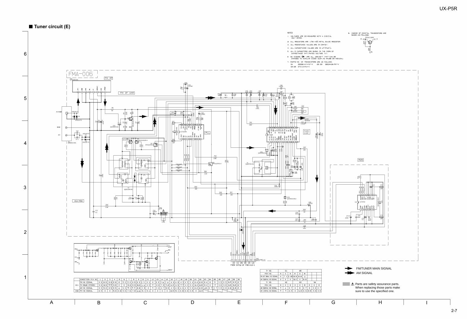
2-7
UX-P5R
IHA B C D E F G
1
2
3
4
5
6
Tuner circuit (E)
FM/TUNER MAIN SIGNAL
AM SIGNAL
Parts are safety assurance parts.When replacing those parts makesure to use the specified one.
TU1
Q4
C52
CF3
R5
CF1
C10
Q2
C51
IC3
C74
C12
C11
R15
R17C14
C15
C13
R16
C75
L70
L3
C16
R29
R41
R21
R28
C54
C22
C72
R27
C25
C6
CF2
C55C56
CN1
C45 R38
C44
C50
C42
R39
C43
R37
C21
C36
R31
C73
C48
C30
C7
R32
C23
C76
C24
C26
C27
C18
D1
R30
T1
C71
C70
D2
D3
L2
D4
C53
C57
C20
Q3
Q5
Q1
L1
C59
C58
C49
J1
C17
R33
R3 R4
R2
C2
R23
R25
IC2
R14
X1
R24
R26
R71
D11
R72
IC1
R73
R10
C46 C47
R34
C34
C32
C31
C40
C35
R36
R12
C39
C38
R35
C37
R18
C41
C33
R19
R20
R22
C19
X70
R70
C4C
1
R11
R13
R40
C3
R6
C9
R60
C60
QAU0160-001
DTA114YKA-X
0.27
QAX0610-001Z
56
QAX0420-001
12P
2SC2412K/R/-X
1/50
LC72723
0.1
LC72136N
0.047
0.1
3.3K
68( 1/4W) FR100/10
12P
12P
4.7K
10/50
100
4.7
12P
10K
3.3K
5.6K
10K
0.047
150P
560P
10K
LA1838
100/10
0.001
QAX0458-001Z
33P10P
QGF1205F1-13
10/16 39K
10/16
22/16
0.0018
39K
0.0018
10K
0.022
1/50
1K
0.1
0.0022
100/10
0.001
1K
150P
330P
150P
0.01
0.01
0.47/50
1SS133-T2
1.2K
QQR0793-001
22P
22P
1SS133-T2
1SS133-T2
33
1SS133-T2
22/16
0.001
1000P
QQR1094-001
2SC2412K/R/-X
DTA114YKA-X
0.001
0.047470P
QNB0014-001
0.0039
330
220K 33
0
330
0.01
1.8K
330
100K
QA
X04
02-0
01
10K
2.2K
1K
1SS
133-
T2
1K 1K
2.2K
0.02
2
1/50
47
0.02
2
0.04
7
22/1
6
10/1
6
0.04
7
3.3K
4.7k
1/50
0.22
/50
5.6k
1/50
1K
10/1
6
0.04
7
1K 1K4.
7K
0.04
7
QA
X02
63-0
01Z
10K
0.010.02
2
4.7k
10K
2SC
2814
/4-5
/-X
39k
10/1
6
12
0.00
1
0
5.6V
RO
UT
LOU
T
RD
DA
RD
CL
ST
ER
EO
CE
D.G
ND
9VCK
DA
TA
GN
D
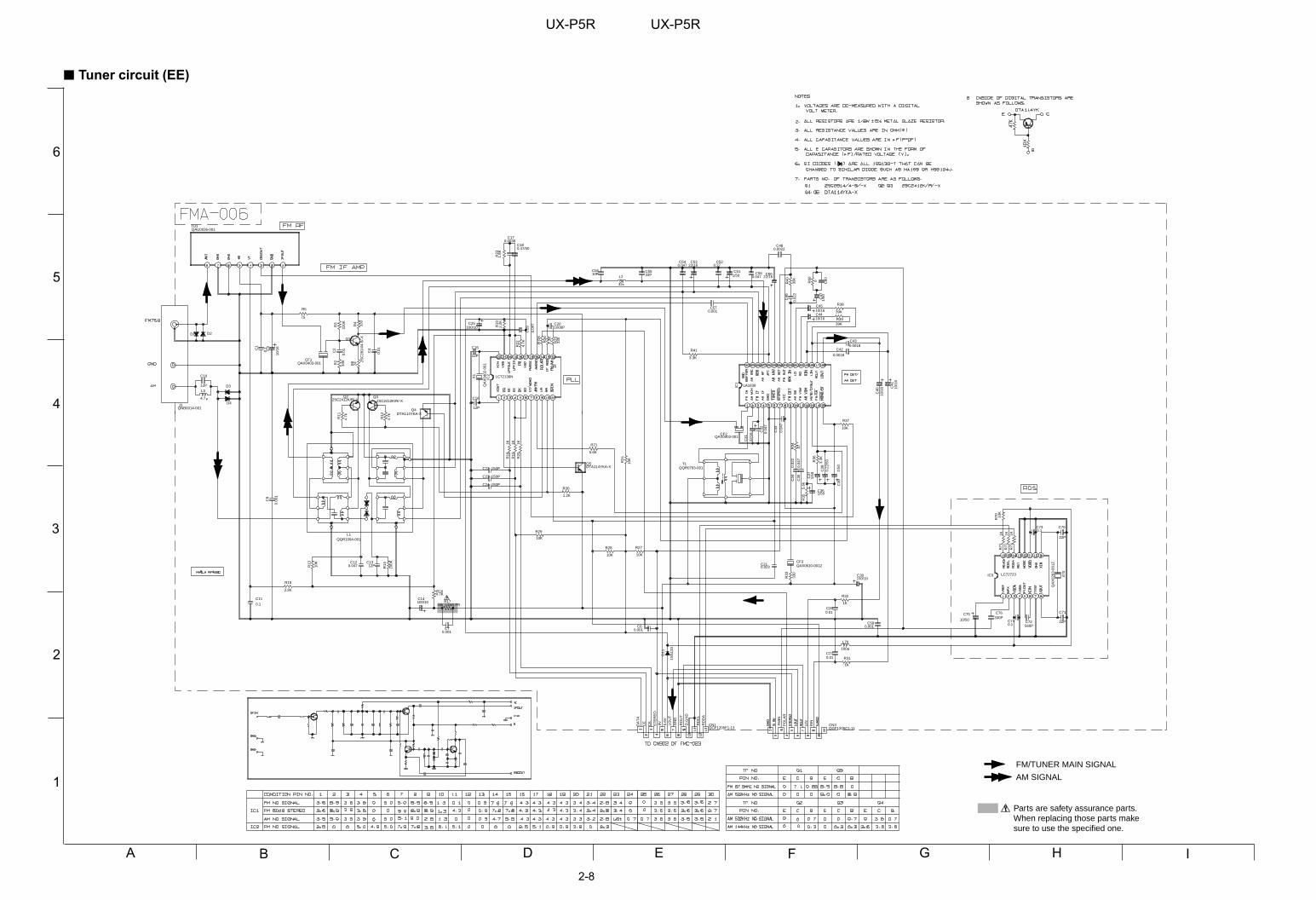
2-8
IHA B C D E F G
1
2
3
4
5
6
UX-P5R UX-P5R
Tuner circuit (EE)
FM/TUNER MAIN SIGNAL
AM SIGNAL
Parts are safety assurance parts.When replacing those parts makesure to use the specified one.
TU1
Q4
C52
CF3
R5
CF1
CN1
Q2
C51
IC3
C74
C12
C11
R15
R17C14
C15
C13
R16
C75
L70
C16
R29
R41
R21
R28
C54
C22
C72
R27
C25
C6
CF2
C55
C7
C26
C45 R38
C44
C50
C42
R39
C43
R37
C21
C36
R31
C73
C48
C30
C27
R32
C23
C76
C24
CN3
C59
C18
D1
R30
T1
C71
C70
D2
D3
C58
D4
C53
C57
C20
Q3
Q5
Q1
L1
C10
L3
C56
L2
J1
C17
R33
R3 R4
R2
C2
R23
R25
IC2
R14
X1
R24
R26
R71
D11
R72
IC1
R73
R10
C46 C47
R34
C34
C32
C31
C40
C35
R36
R12
C39
C38
R35
C37
R18
C41
C33
R19
R20
R22
C19
X70
R70
C4C
1
R11
R13
R40
C3
R6
C9
R60
C60
R7
QAU0036-001
DTA114YKA-X
0.27
QAX0610-001Z
75
QAX0403-001
QGF1205F1-13
2SC2412K/R/-X
1/50
LC72723
0.1
LC72136N
0.047
0.1
3.3K
68( 1/4W) FR100/10
12P
12P
4.7K
10/50
100
12P
10K
3.3K
5.6K
10K
0.047
150P
560P
10K
LA1838
100/10
0.001
QAX0403-001
33P
0.001
0.01
10/16 39K
10/16
22/16
0.0018
39K
0.0018
10K
0.022
1/50
1K
0.1
0.0022
100/10
0.01
1K
150P
330P
150P
QGF1205C1-11
0.001
0.47/50
1.2K
QQR0793-001
22P
22P
0.047
22/16
0.001
1000P
QQR1094-001
2SC2412K/R/-X
DTA114YKA-X
12P
4.7
10P
33
QNB0014-001
0.0039
330
220K 33
0
330
0.01
1.8K
330
100K
QA
X04
02-0
01
10K
2.2K
1K
1SS
133
1K 1K
2.2K
0.02
2
1/50
47
0.02
2
0.04
7
22/1
6
10/1
6
0.04
7
3.3K
4.7k
1/50
0.22
/50
5.6k
1/50
1K
10/1
6
0.04
7
1K 1K4.
7K
0.04
7
QA
X02
63-0
01Z
10K
0.010.1
4.7k
10K
2SC
2814
/4-5
/-X
39k
10/1
6
24
0.00
1
0
1K
5.6V
RIN
LIN
RD
DA
RD
CL
ST
ER
EO
D.G
ND
LOU
T
CE RO
UT
9VCK
DA
TA
FM
IN
GN
D
PO
LAR
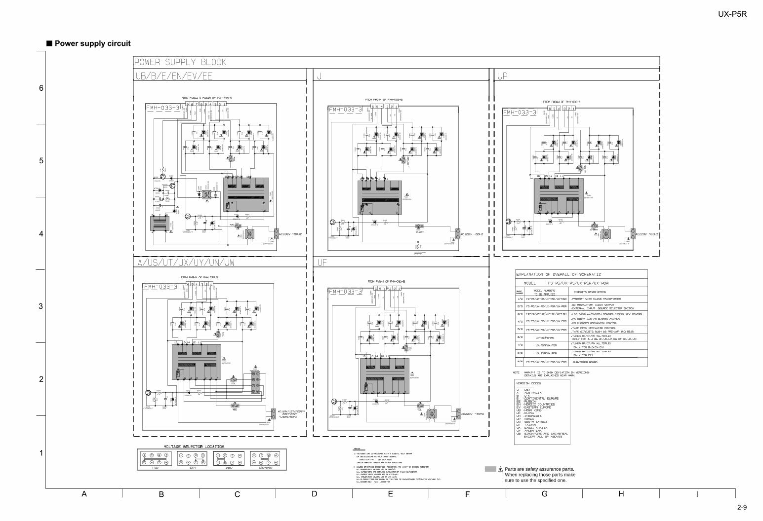
2-9
UX-P5R
IHA B C D E F G
1
2
3
4
5
6
Power supply circuit
Parts are safety assurance parts.When replacing those parts makesure to use the specified one.
S1000
F1002
F1000
C1010
C1011
C1009
T1000
Q1002
F1000
J1000
Q1002
D1011
J1000
D1012 R1003
F1000
C1012
J1000
EP940
D1010Q1000
T1000
R1002
Q1001
R1004
C1012
R1004 D1012 R1003
T1000
Q1002
D1012 R1003
C1012
R1004
Q1002
D1012 R1003
C1012
R1004
F1000
T1000
J1000
Q1002
D1012 R1003
C1012
R1004
F1000
J1000
C10
00
C10
08
C10
00
C10
01
C10
03
D10
01
D10
02
D10
03
C10
01
C10
03
D10
01
C10
02
CN
950
D10
00
T10
01
D10
08
D10
02
D10
03
RY
940
C10
02
D10
00
D10
09
CN
950
C10
00
CN
951
C10
05
C10
04
C10
07
D10
04
D10
06
D10
07
C10
06
D10
05
C10
01
CN
951
L100
0
C10
05
C10
04
C10
07
D10
04
D10
06
D10
07
C10
06
D10
05
C10
03
D10
01
D10
02
D10
03
R10
00
C10
02
D10
00
D10
13
T10
00
C10
05
C10
04
C10
07
D10
04
D10
06
D10
07
C10
06
D10
05
C10
00
C10
01
C10
03
D10
01
D10
02
D10
03
C10
02
D10
00
D10
13
R10
01
R10
05
C10
05
C10
04
C10
07
D10
04
D10
06
D10
07
C10
06
D10
05
R10
05
CN
951
D10
13
R10
05
CN
950
D10
13
R10
05
CN
950
CN
951
C10
00F10
01
F10
01
F10
01
C10
01
C10
03
D10
01
D10
02
D10
03
F10
01
L100
0
C10
02
D10
00
C10
05
C10
04
C10
07
D10
04
D10
06
D10
07
C10
06
D10
05
D10
13
R10
0R
CN
950
CN
951
F10
01
CN
949
L100
0
QSW0812-001
470/16
1000/25
0.0047
QQT0323-003
KTC3199/GL/-T
QGA7901C1-02
KTC3199/GL/-T
MTZJ6.2A
QGA7901C1-02
1SS133-T2 10K
22/50
QGA7901C1-02
1SS1332SC2785
QQT0323-003820
2SC2235
4.7K
22/50
4.7K 1SS133-T2 10K
KTC3199/GL/-T
1SS133-T2 10K
22/50
4.7K
KTC3199/GL/-T
1SS133-T2 10K
22/50
4.7K
QQT0323-001
QQT0323-003
QGA7901C1-02
KTC3199/GL/-T
1SS133-T2 10K
22/50
4.7K
QGA7901C1-02
0.1u
QC
Z91
05-4
72
0.1u
0.1u
0.1u
IN40
03S
-T5
IN40
03S
-T5
IN40
03S
-T5
0.1u
0.1u
IN40
03S
-T5
1N40
03S
-T5
0.1u
QG
D25
04C
1-03
Z
T02
53-0
02
1SS
133
1N40
03S
-T5
1N40
03S
-T5
OS
K01
24-0
01
1N40
03S
-T5
0.1u
IN40
03
QG
D25
04C
1-03
Z
0.1u
QG
D25
04C
1-03
Z
0.1u
0.1u
0.1u
1N54
01-T
M
1N54
01-T
M
1N54
01-T
M
1N54
01-T
M0.
1u
0.1u
QG
D25
04C
1-03
Z
R07
99-0
01
0.1u
0.1u
0.1u
1N54
01-T
M
1N54
01-T
M
1N54
01-T
M
0.1u
1N54
01-T
M
0.1u
1N40
03S
-T5
1N40
03S
-T5
1N40
03S
-T5
3.3M
1N40
03S
-T5
0.1u
MT
ZJ5
.1B
-T2
T03
23-0
02
0.1u 0.1u
0.1u
1N54
01-T
M
1N54
01-T
M
1N54
01-T
M
1N54
01-T
M0.
1u
0.1u
0.1u
0.1u
1N40
03S
-T5
1N40
03S
-T5
1N40
03S
-T5
1N40
03S
-T5
0.1u
MT
ZJ5
.1B
-T2
3.3K
4.7K
0.1u 0.1u
0.1u
1N54
01-T
M
1N54
01-T
M
1N54
01-T
M
1N54
01-T
M0.
1u
4.7K
QG
D25
04C
1-03
Z
MT
ZJ5
.1B
-T2
4.7K
QG
D25
04C
1-03
Z
MT
ZJ5
.1B
-T2
4.7K
QG
D25
04C
1-03
Z
QG
D25
04C
1-03
Z
0.1u
0.1u
0.1u
1N40
03S
-T5
1N40
03S
-T5
1N40
03S
-T5
R07
99-0
01
1N40
03S
-T5
0.1u
0.1u 0.1u
0.1u
1N54
01-T
M
1N54
01-T
M
1N54
01-T
M
1N54
01-T
M0.
1u
MT
ZJ5
.1B
-T2
4.7K
QG
D25
04C
1-03
Z
QG
D25
04C
1-03
Z
QG
D25
04C
1-03
Z
R07
99-0
01
A.G
ND
A.G
ND
VL
VH
-VH
VH
-VH
INH
B
PO
UT
A.G
ND
INH
B
INH
B
VLIN
HB
D.G
ND
VH
-VH
VL VH
-VH
VL
A.G
ND
-VH
ST
NB
Y
VH
VL
A.G
ND
INH
B
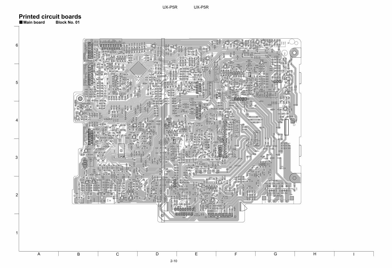
2-10
IHA B C D E F G
1
2
3
4
5
6
UX-P5R UX-P5R
Printed circuit boardsMain board Block No. 01
/tr/p/jem/10011-001A/10011A [01.1.18-10:47] Create by Kops
C2000
C2003
C20
05
C20
06
C2007
C2008
C2009
C2010
C20
11
C2012
C2013
C2014
C2015
C20
16
C20
17
C2018C2019
C2020
C2021
C2022
C20
23
C20
24
C2025
C20
27
C21
28
C2029
C2030
C20
31
C2032
C2033
C2034
C2035
C2036
C2037
C2100
C2103
C2105
C21
06
C21
07
C2108
C21
09
C21
10
C21
11
C21
12
C21
13
C21
14
C21
15
C21
16C
2117
C21
18
C21
19
C2120
C2121
C2122
C2123
C21
24
C2125
C2127
C2028
C2129
C21
30
C2131
C2132
C2133
C2134
C21
35
C2136
C21
37
C22
00
C22
07
C2209
C2211
C2212
C22
13
C22
14
C22
15
C2217
C22
18
C22
19
C2220
C22
21
C22
22
C22
24
C2225
C2226
C2227
C22
28
C22
29
C22
30
C2231
C22
32
C2233
C2234
C22
35
C2236
R2232
C22
39
C3202
C3203
C3204
C3205
C3206
C3222
C3223
C7001
C7002
C7003
C7004
C7005
C7006
C7007
C70
08C70
09
C7010
C7011
C70
12
C7041
C7061
C70
62
C70
63
C7108
C7111
C71
13
C71
15
C7123
C71
28
C71
35
C71
36
C71
44
C71
49
C71
52
CN
900
CN
901
CN
902
CN
903
CN
904
CN
905
CN913
CN906
D7010
CN
907
C20
26
C2126
D2200
D2201
D22
02
D22
03
D22
04
D2205
D2206D
2208D2210
D22
11
D22
12
D22
13
D22
14
D22
16
D2218
D22
22
J900
D3218
D32
19
D32
20
D3221
D70
01
D70
02
D70
03
D7004D7005
D7006
D7007
D7008
D7061
D70
71
IC90
1
C20
38
C2138
IC905IC910
IC932
FW90
2
J902
K700
1
K700
2
K7003
L220
0
L220
1
L700
1L700
2
L7003
Q70
01
Q7003
Q7041
Q70
92
Q22
11
Z3002 Z3001
R2000R2001
R71
61
R2003
R2004
R2005
R2006
R2007
R2008
R2009
R20
10R
2011
R20
12
R2013
R20
14
R20
15
R20
16R
2017
R20
18
R2019
R2020
R2021
R2022
R20
23
R2024
R20
25
R20
26
R20
27
R20
28 R20
29
R20
30
R2031
R20
32
R2033
R2034
R2035
R2036
R20
37
R2038R2039
R20
40
R2041
R20
42
R20
43
R71
62
R2047
R20
48
R2049
R2100R2101
R2103
R21
04
R2105
R2106
R2107
R2108
R2109
R21
10
R21
11
R2112
R2113
R2114
R2115
R2116
R21
17
R2118
R2119
R2120
R21
21
R2122
R21
23
R2124
R21
25
R21
26
R2127
R21
28
R2129
R21
30
R2131
R21
32
R21
33
R2134
R21
35
R21
36
R21
37
R21
38
R2139
R2140
R2141
R21
42
R21
43
C25
00
R2147
R21
48
R21
49
R2200
R2207
R2208
R22
09
R22
11
R22
12
R2213
R22
14
R2216
R2217
R22
18
R2219
R2220
R22
21
R2222
R2223
R2224
R22
28
R22
29
R3201
R32
02
R32
03
R32
04
R32
05
R32
06
R70
01
R70
02
R70
03
R70
04
R70
05
R70
06
R70
07
R70
08
R70
41
R70
42
R7043
R7062
R7064
R70
65R7075
R7076
R7077
R7078
R70
91
R70
92
R70
93
C2505
R7101
R71
02
R71
03
L2500
L2501
R7106
R7107
R7108
R7109
R7110
R7111
R7112
R7113
R7114
R7115
R7116
R71
17
R71
18 R71
19
R71
20
R7121
R71
22
R7123
R71
24
R71
25
R71
26
R71
27
R71
28
R71
29
R71
30
R71
31
R71
32
R71
33
R71
34
R71
35
R71
36
R71
37
R71
38
R71
39
R71
40
R7141
R71
42
R7143
R71
44
R71
45
R71
46
R71
47
R71
48
R71
50
R7151
R7152
R7153
R71
54R
7155
C25
01
C2502R
7201
R7202
R7203
R7206
R72
14
R72
15
R72
17
R72
18
R7236
R72
38
R7232
R72
39
R72
40
R72
47
R72
52
R72
53
R7254
R7255
R3200
X700
1
X700
2
IC903
IC90
4
IC902
J901
Q2204
Q2205
Q22
06
Q2207
Q2209 Q2210
Q2212Q2213
Q2215 Q2216
Q2219
Q22
20
Q22
22 Q22
24
D3222
R32
08
CN931
R3209
Q70
61
Q7062
Q70
91
Q70
02
Q2217
Q22
14
Q2203
Q22
08
C7013
C2508
R22
30
CN
933
R71
58
R7159
R7160
Q74
01
Q74
02
Q74
03
R7149
C2509
C2506
C25
03
R7079
FW90
1
C2507
R22
31
Q70
31
R70
09
D7009
R7010
C2504
R71
57R
7156
R72
21
PP95
0
R2144
R20
44
C2039
Q3501
Q35
02
Q3500
FW90
4
C35
02R
3504
R35
05R
3500
D35
01
D22
07
L3500
CN908
C35
00
C35
01
R35
02R
3503
R35
06
D35
00Q3503
R35
01
W951
C2139
Q2218
Q2221
R70
00
R3207
K2200
R+ L-L+ R-
1 14
1
21
41
61
1918
36
TUST/CECKMPX/ST9V5.6VLOUTTUGROUT
TUDATA
CDRAGAGCDLCD+BCD+BCL-SWOP-SWOPENCLOSE
SW9VSW9V
MG
STTA/RSTSQCKSUBQDGMCLKMDATAMLD
FLAGMUTE
1
AUXO
UT
R L R L
AUXI
N
US5
VLE
DG
ND
DIM
MER
BASS
+KE
Y0KE
Y1D
G/R
EM5
12
1
2
VOL-
BASS
-
VOL+
LED
CTL
[]
113
161
1
15
1
/REST
15
1
7
8
SUBR
AHBIN
VL.GND
VL
FW901
POUT
SUBTR.G
FW902
1
4
5
7
CN907
1
4
CN905
D.OUT
DG
+B
6V[SUB]
BLKCKDGDG
SCDSCD
13
RDDARDCLDGDG 9
1
1
3
31
17
FW90
4
BE
C
BE
C
BE
C
C
B E
C
EB
BE
C
E
C
BE
B
C
E
C
B
EB
C
EB
C
BE
1 8
54
B
C
E
B
C
E
LEDFRUS5V
CN933
LEDRECLEDRV
1
4
41
CN901
PHOTOPLAYKEY1SAFETY1DGSCKUS5VSDATASTTA
MGSW9VNCPBRAGPBLSW8VRECRNCRECL
CN9001
9
1
10
110
9
1
B
C
E
B
C E
B
C
E
1
45
8
B
C
EB
C
E
B
C
E
GNDGND
VL
VL
41
FANNG
PRT
SUBL
AG
[P5/
P7]
[P3]
[P5/
P7]
4
1
8
1
B
C
E
B
C
E
B
C
E
B
C
E
B
C
E B
C
E
B
C
E
B
C
E
1 4
B
C
E
1
45
8
41
LIN
RIN
HPS
W
CN
913
H/P
.GN
D
LIN
H/P
.GN
D
CN
906
LOU
T
RO
UT
RIN
51
B
C
E
T001
A
B
C
E
B
C
B
C
E
B
C
E
E
B
C
E
EB
C
[]
SMUTEVH.GND
SPKMUTE
9V
F3000
SCL
MO
DE
/INH
LCD
CE
DAT
A
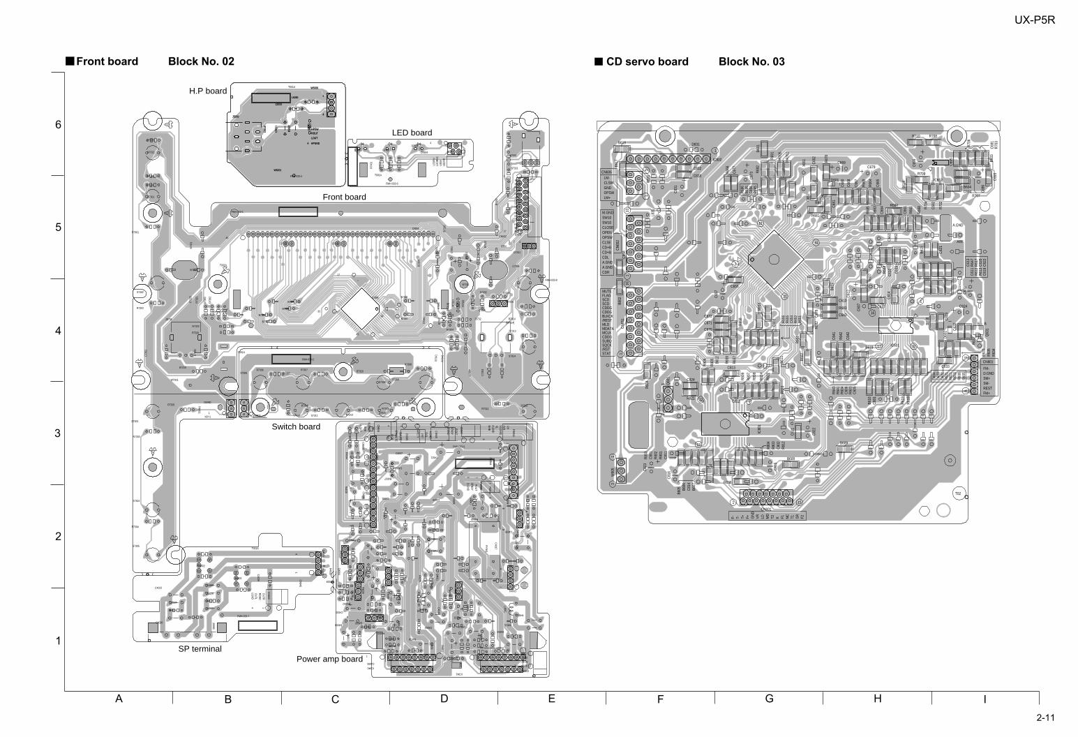
2-11
UX-P5R
IHA B C D E F G
1
2
3
4
5
6
CD servo board Block No. 03Front board Block No. 02
LED board
H.P board
Front board
Switch board
SP terminalPower amp board
FMH-033-6
FMH-033-1
FMH-033-2
FMH-033-7
FMH-033-8
FMH-033-5
FMH-033-4
T001A
T001
A
T001A
T001A
T001A
T001A
CN
943
JA940
C4027
C4039
C4024
C4026
C4025
R4025
R4024
C4022C4023
L4003
L4002
LGN
DO
UTL
RG
ND
OU
TR
CN
943
14
14
C73
01
C7303
C7305
C7306
C73
41
C73
51
C73
52
C73
53
C73
54B7
303
B7313
B7312
B731
7
D7331
D7332
DI934
IC933
IC934
JS731 JS732
K734
1
Q7331
R7301
R7302
R7303
R7304
R7305
R7311
R7312
R7313
R7314
R7315
R7321
R73
22
R7323
R73
31
R73
32
R73
41
R73
42
S7301
S7302
S7303
S7304
S7305
S7312
S7313
S7314
S7315
CN932
B730
2
B730
5
B7301
B7306
B7307B7310
B7308
B7311
B7309
B730
4
B731
6
D7321D7322D7323
B732
1
B7319
B732
2
FW931
W7001
D73
61
D73
62
D73
63
40 1
33
1
REMDGNDKEY1KEY0BASS+VOL-BASS-
US5VLEDGNDDIMMER
17
[B7314]
[B73
18]
LEDCTLV0L+
R7324R7326
REDGRN
123
1
R73
25
KEY1
DGND
1
49
BE
17
64
LCDCE
INHSCLMODEDATA
C4020
C4021
Q4006
CN941
FW944
C4016
C4017
C4014
C4015
C4011
C4009
C4006
C4002
C4013
C4018
C4019
C4000
C4001
C4004
C4005
D4009
R4044
D40
05
D4007
FW945
C4036
D4002
D4003
R4029
R4030
R4031
D4000
R4032
IC940
IC941
R4033
R4034
L4001
L4000
R4035
C4028
C4029
C4030
Q4003
Q4004
Q4005
R4040
R4041
R4037
C4031
R4038
C4034
C4035
D4006
RY941
D4008
R4042
R4043
CN
944C
N945
CN
946C
N947
R4015
R4017
R4016
R4019
R4018
R4013
R4012
R4011
R4010
R4008
R4006
R4023
R4022
C4037
C4038
R4021
R4020
R4026
R4027
Q4001
Q4000
C4012
R4000 R4001
R4004
R4005
R4003
R4002
EB
1 15 1
154
13
14
14
14
1
LGND
OUTLRGND
OUTR
CN941
4
1
14
SMU
TE
SIGR
9V
SPKMU
TE
AHB
A.GN
D
VL[GN
D]
VL
CN
944
CN
945
POU
T
D.G
ND
STNBY
FW945
B E
16
1
FW944
79
97
VL[GN
D]
INH
BA.G
ND
VL
+VH-VH
BE
BE
E
BE
B
B
CN
946
A.GN
D
SIGL
PRT
SAFETY
14
3 1
CN
947
POU
T
STNBY
D.G
ND
6
41
S7309S7308
S7307S7306
S7310S7311S7316
R7308
R7306
R7316
R7310
R7307
R7309
C7304
B7320
FW9311
D7403
D7402D7401CN934
R74
01
R74
02
R74
03
1
4
LED
RV
LED
REC
US5
VLE
DFR
C50
10
J5000
K502
2
L5030
L5033
W5000
ROUT
LOUT
1
HPGND
HPSW
C50
11
W5001
4
4
1
C50
10
J5000
K502
2
L5030
L5033
W5000
ROUT
LOUT
1
HPGND
HPSW
C50
11
W5001
4
4
1
C60
1
C60
2C
603
C60
4
C60
5
C60
6
C60
7
C610
C61
1
C61
2
C61
3
C61
4
C61
5
C61
6
C617
C61
9C
620
C62
1
C62
2
C62
3
C624
C63
1
C63
2
C633
C64
1
C64
2
C643
B619
C65
1
C65
2
C65
3
C65
4
C655
C65
6
C65
7
C65
8
C66
1
C66
3
C66
4C
665
C66
7
C66
8
C669
C670
C671
C672
C67
3
C67
6
C67
7 C679
C68
0
C69
1
C69
2
C69
3
C694
C69
5
C69
6
C69
9
C80
1
C80
2
C81
1
C812
C813
C81
4
C81
5
C82
1
C82
2
C82
3
C824
C83
1
C832
C833
CN601
CN
651
CN
652
CN801
D831
R64
8
IC652
IC80
1
IC802
L831
Q63
1
Q80
1
R60
1R
602
R60
3
R60
4
R60
5R
606
R61
0R
611
R61
2R
613
R61
7
R61
8
R61
9
R62
0
R62
1
R63
1
R63
2
R63
4R
635
R636
R64
1R
642
R64
3
R64
7
R65
1R
652
R65
3
R65
4
R65
5R
656
R65
7
R65
8
R65
9
R66
1
R66
2
R66
3R
664
R66
5
R66
6
R667
R66
8
R66
9
R67
0
R68
2
R683
R68
5
R69
1
R69
2
R69
5R
696
R70
1
R70
2
R70
3
R70
4
R70
5
R70
6
R707
R708
R709
R710
R80
1R
802
R80
3R
804
R80
5
R80
6
R80
7
R80
8
R80
9
R81
2
R821
R82
2
R82
3
R82
4
R83
1
W60
5
CN606
X651
B604
B616
B614
R81
3
C81
6
B613
B615
B610
B612
B617
B618
IC601
R60
7
B601
B603
B602
B611
B609
B608
B607
B606
B605
D601
D60
2
R681
C68
1
R684
MUTEFLAG
CDDG
BLKCK/RESTMLDMDATAMCLKCDDGSUBQSQCK/RSTSTAT
FM+RESTSM-SM+D.GNDFM-
1
1
1
1
1
BE
BE
C
31
6
ARF
A.GND
F- T- T+ F+ GN
DVR LD M
DT2 K F1 N
CT1 SR F2
1 15
T02
SCDSCD
CDDG
13
LM+OPSWGNDCLSWLM-
M.GNDSW10SW10CLOSEOPENOPSWCLSECD+BCD+BCDLA.GNDA.GNDCDR
51
116
1
21
41
61
17
16
32
12
2413
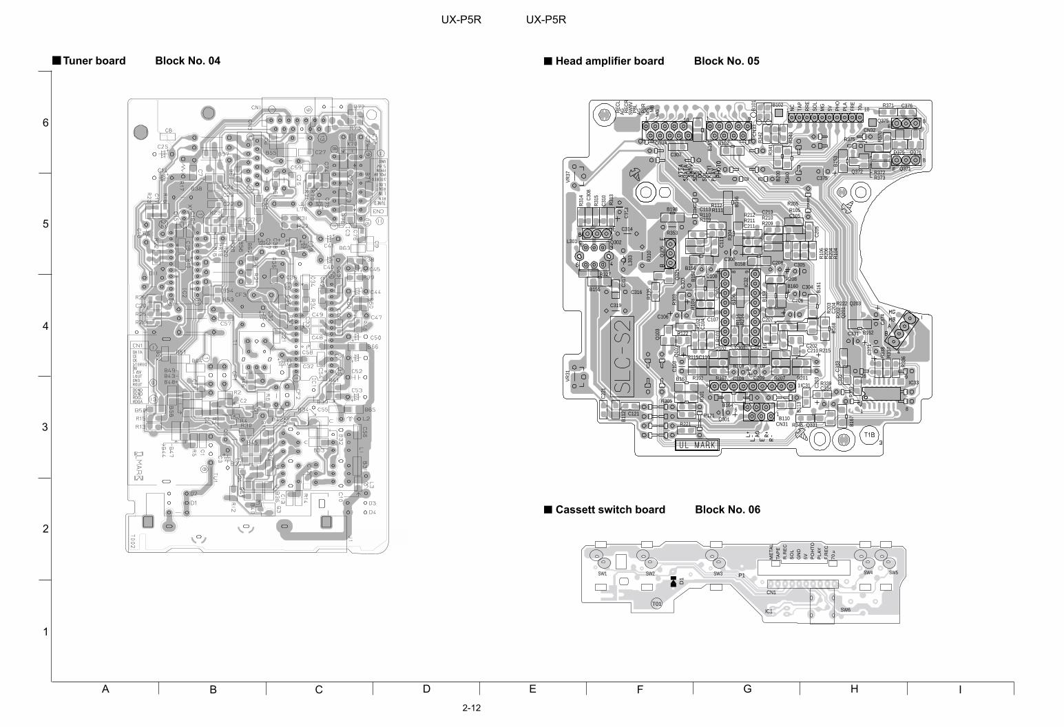
2-12
IHA B C D E F G
1
2
3
4
5
6
UX-P5R UX-P5R
Head amplifier board Block No. 05Tuner board Block No. 04
C202
C376
C10
3
C121
C106
C305
C108
C109
C107
C30
8
R20
3
C30
2
C20
3
R109
C206
R10
4
C209
C113
R209
C207
C301
C31
0
C30
3
C304
C208
C331
C31
3
R11
6
R20
4
C316
B10
6
C319
R10
3
C375
61
CN31
B158
70u
FRE
PLA
PH
O5VM
GS
OL
RR
ETA
PN
C
1 10
CN32
9 1IC31
8 9IC
32
1 16
16
1 8
9IC33
L301
Q10
1
Q20
1
Q30
5
Q302
B16
8
C334
BQ375E
Q376
Q371
B
E
C201
R101
R10
2C
104
R105
R10
6
R107
R10
8
C22
1
R110R111R112
R121
R201
R20
2C
204
R205
R20
6
R207
R208
C11
1
R210R211R212
R221
R30
1
R30
3
R30
4
B16
7
R33
5
R31
5
R31
4
R31
3
R31
0
R122
Q10
3
R305
B15
1
R371
R375 R37
6
R372
R33
8R
337
R34
1
R34
2
R34
3
R339
R33
6
R33
1
VR
31V
R37
C210C110
C102 C101
Q372
C213
C211
R215
D375
R115
R34
0
Q331
B11
3
R345
9
CN
33
11
CN34
MS M
B
PB
RA
GPB
LS
W8V
RE
CR
AGRE
CL
MG
10
R327
C306
R21
6
C37
1
B15
3
B152
B162
C37
4
R222
B102
B20
0
B10
1
Q203
B110
B109B108
B164
B16
1
B163
R353
B155
C31
7
C314
L303
R373
B15
7
B15
9
B156
B160
B11
2
C307
B16
6
Q32
1
B198C105
C20
5
C33
2C
333
Cassett switch board Block No. 06
SW1 SW2 SW3 SW4 SW5P1
D1
IC1
CN1
SW6T01
Related Documents