ASIC Design Services Nevatron Ltd

Welcome message from author
This document is posted to help you gain knowledge. Please leave a comment to let me know what you think about it! Share it to your friends and learn new things together.
Transcript

ASIC Design Services
Nevatron Ltd

2
Services
ASIC design (Front-end & Back-end)
ASIC verification (functional/formal)
FPGA design/prototyping & FPGA to ASIC conversion
IP blocks creation
CAD libraries development
PDK development

3
Engineering staff
The unit currently employs nine engineers
Four engineers have worked at western design centers in Russia
Three engineers have worked abroad (USA, Austria, Sweden, Scotland, South Korea, India)
Two engineers have passed trainings at Cadence (Munich), one at Synopsys (Stockholm)

4
Our key specialists
Vasily Atyunin:
Senior ASIC designer
Project manager, CTO
Worked in South Korea, India and Scotland
Sergey Dedov:
Senior ASIC designer
Worked in Sweden and Scotland
5
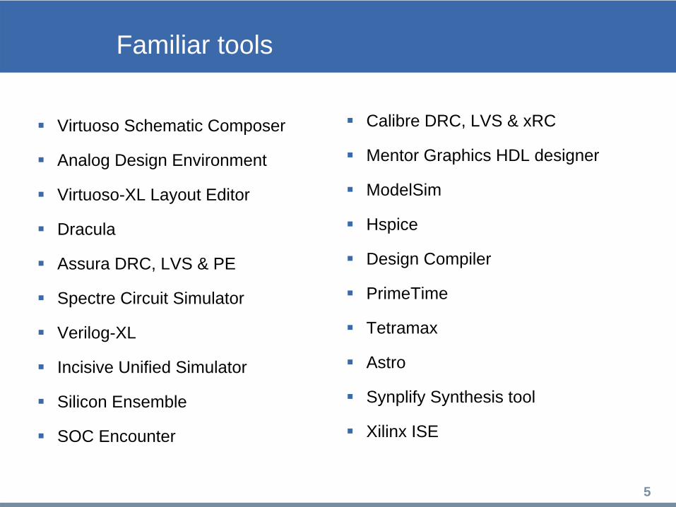
Familiar tools
Virtuoso Schematic Composer
Analog Design Environment
Virtuoso-XL Layout Editor
Dracula
Assura DRC, LVS & PE
Spectre Circuit Simulator
Verilog-XL
Incisive Unified Simulator
Silicon Ensemble
SOC Encounter
Calibre DRC, LVS & xRC
Mentor Graphics HDL designer
ModelSim
Hspice
Design Compiler
PrimeTime
Tetramax
Astro
Synplify Synthesis tool
Xilinx ISE

6
Quality Management System
Our company strives to follow ISO9001 standards. Our Quality System contains standards, procedures and guidelines which represent good design practice. It provides full traceability of all design and production decisions, experimental results and project functions (utilizing project management, back-up/archiving and log-book systems). The Staged Design Review system verifies product quality during design process:
Initial Circuit Design Review (checks feasibility and proposed circuit structure)
Intermediate Circuit Design Reviews according to the Project Plan (assures that all functional and performance requirements will be met)
The final Circuit Design Review (checks full compliance of product to customer requirements)

7
Project Management and Reports
The Project Manager divides the project into subtasks and allocate them to team members after initial Circuit Design Review
A Gantt chart for the project is issued by a Project Manager after initial Circuit Design Review
All work on the project is tracked by the Project Manager every day. Progress reports can be send to a customer according to agreed time schedule.
Design information (schematics, current database, GDS, etc) can be send with progress reports as well
Circuit Design Review presentations (with simulation results, etc) can be sent to a customer upon completion

8
Supported Design Flow Stages 1. System architecture and planning
Project Planning
System Development Budget Definition Tools Selection Project Scheduling (Gantt chart)
Architecture
SystemC Modelling
Technology Evaluation
IP Core Evaluation
Mathematics Modelling/Simulation
Design Partitioning & FloorPlanning
Test Methodology Determination
Detailed Specification Development

9
Supported Design Flow Stages 2. Front-end implementation and verification
Implementation
Behavioral model development
RTL model development
Schematic entry
Soft/hard macros development
Test benches development
Functional/formal verification
DFT insertion
Scan chain insertion
BIST insertion
Automatic Test Pattern Generation (ATPG)
Synthesis and Timing Analysis
Constraints Development
Synthesis
Static Timing Analysis
Virtual or FPGA Prototyping
10
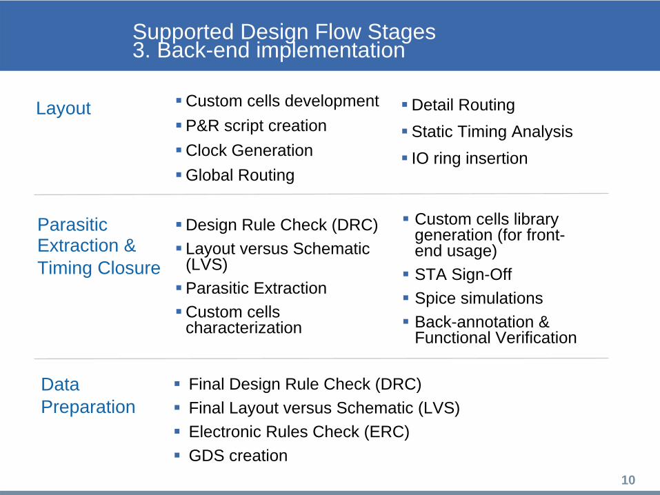
Supported Design Flow Stages 3. Back-end implementation
Layout
Custom cells development
P&R script creation
Clock Generation
Global Routing
Parasitic Extraction & Timing Closure
Data Preparation
Final Design Rule Check (DRC)
Final Layout versus Schematic (LVS)
Electronic Rules Check (ERC)
GDS creation
Detail Routing
Static Timing Analysis
IO ring insertion
Design Rule Check (DRC)
Layout versus Schematic (LVS)
Parasitic Extraction
Custom cells characterization
Custom cells library generation (for front- end usage)
STA Sign-Off
Spice simulations
Back-annotation & Functional Verification

11
IP development
Libraries Creation
Cell Characterization
LIB (TLF, ALF) File Creation
LEF File Creation
PDK Development
Tech File Development
P-Cells Development
CDF Development
Verification Decks Development
Schematic Creation
Pre-layout Simulation
Layout
Post-layout Simulation
Custom Cell Development

12
Recent projects
The receiver consists of a bandpass sampler and a pipeline ADC
Clock frequency is 400MHz (several identical receivers are to be used in parallel to receive higher frequencies)
TSMC 40nm low power CMOS technology
Design Flow: Virtuoso Front to Back Design Environment, Calibre DRC/LVS, Spectre
Project: Development of analogue front-end of 12-bit digital receiverClient: A US company
The development involves six people (two circuit designers, two layout engineers, one verification engineer and a project manager)
The development is in progress now

13
Recent projects
The transmitter consists of analogue and digital parts
The analogue part contains full custom driver, serialiser, VCOs, PLLs, ESD circuits, replica circuits and test circuits
UMC 0.18um standard CMOS technology
Design Flow: Schematic Composer, Virtuoso XL, Assura DRC/LVS, Spectre, SOC Encounter
Project: Development of UWB short-range transmitterClient: A Russian company
The design was done by four people (one circuit designer, one layout engineer, one verification engineer and a project manager)
The test chip was successfully evaluated

14
Recent projects
The design was done from specification down to GDS
The family includes several devices which differ only with M3 masks
TowerSemi 0.6um standard CMOS technology
Design Flow: Schematic Composer, Virtuoso XL, Assura DRC/LVS, Spectre
Project: Design of I2C-bus/SMBus buffersClient: A US company
The design was done by four people (one circuit designer, one layout engineer, one verification engineer and a project manager)
The chip is to go in mass production now

15
Recent projects
Dual gate 0.18um 5V/1.8V CMOS TowerSemi technology
2KV HBM ESD protection level
All cells are over-voltage tolerant
There are two versions: 3LM and 4LM
Design Flow: Schematic Composer, Virtuoso XL, Assura DRC/LVS, Spectre
Project: Development of 0.18um High-Power IO libraryClient: An Israel company
The design was done by four people (two layout engineers, one verification engineer and a project manager)
The development took eight weeks totally
The library is officially released to customers

16
Recent projects
The block is 8-bit successive approximation analog-to-digital converter
Vanguard 0.5um HV CMOS technology
The ADC includes input multiplexer, programmable gain amplifier, sample-and- hold circuit, two-stage DAC
Design Flow: Schematic Composer, Virtuoso XL, Assura DRC/LVS
Project: Layout of ADCClient: A Swiss company
The layout was done by three people (two layout engineers and a project manager)
The layout took four weeks totally

17
Recent projects
Vanguard 0.25um HV CMOS technology
The block includes bandgap reference, PTAT and CTAT current sources
Design Flow: Schematic Composer, Virtuoso XL, Assura DRC/LVS
Project: Layout of Bias Control BlockClient: A Swiss company
The layout was done by three people (two layout engineers and a project manager)
The layout took two weeks totally
18
Recent projects
0.5um HV CMOS 2P3M POLYCIDE 5V/40V technology
The PDK includes the following P-cells: various contacts, conventional nmos/pmos, nmos ESD, asymmetric HV nmos/pmos, isolated HV nmos, symmetric HV nmos transistors, poly capacitor, various resistors
The PDK P-cells support such features as multi- fingered transistors, parameterized source/drain contacts, parameterized source/drain to gate distances, matrix of series resistors, guard rings, etc
Design Flow: Schematic Composer, Virtuoso XL, Assura DRC/LVS
Project: 0.5um High Voltage PDK developmentClient: A Swiss company
The development was done by three people (two engineers and a project manager)
The development took three months totally
19
Instruction set fully compliant with ARM Vector Floating Point Coprocessor
Instruction set for single and double precision arithmetic
IEEE 754-1985: 4 rounding types
Hardware implementation for calculation with denormalized number and for underflow exception.
Design Flow: Incisive Unified Simulator, Xilinx Foundation ISE
Project: FPU project – floating point coprocessor core Client: Government work
FPU was prototyped with Xilinx Virtex FPGAs
The development took twelve months totally
Recent projects
20
Former projects
High-speed part (internal operating frequencies up to 430 MHz) Verilog and schematic based synthesis of modules for ASIC layout (TSMC 0.18um technology), TCL scripts, Verilog functional and timing simulation, some Analog Spice simulations
Low-speed part (156.25 MHz MAC and 133.33 MHz PCI-X frequencies): Verilog-based design of PCI X modules (DMA controller application-dependent part, other peripherals), modules of PCI MAC and reverse resynchronization, synthesis (TSMC 0.18um technology), TCL scripts, functional and timing simulation, PLI/VPI with C usage
Design Flow: Viewlogic Workview Office, Ambit BuildGates, ModelSim, Chronologic VCS, Dolphin, HSPICE
Project: Design of 10 Gbps Ethernet NIC (to be used with 10Gbps PHY) Client: Internal R&D
Ethernet NIC was prototyped with Xilinx Virtex FPGAs
Two computers were successfully linked using Xilinx RocketPHY as PHY and Intel XFP module as optical interface
21
Former projects
The Marketing Requirements Specification was developed to a White book, Blue book, Green book according to the QA procedure
TSMC 0.18um standard CMOS technology
Full custom amplifier, deserialiser, VCOs, PLLs, serialiser, driver, ESD circuits, DACs, replica circuits and test circuits
The custom part has 5 GHz link interface and 430 MHz core logic interface
Design Flow: Schematic Composer, Virtuoso XL, Calibre DRC, LVS & xRC, Ambit, Dolphin, HSPICE, ModelSim.
Project: Design of Proprietary High-Speed Link (10 Gpbs PHY)Client: Internal R&D
10 Gpbs PHY test chip transmitter showed up to 14 Gbps data rate
The receiver had some problems with crosstalk from CMOS IO cells on the very input

22
Former projects
DSP was synthesized from RTL VHDL description (about 150 modules)
DSP core architecture has got the Best Product prize at the New Product Forum GSPx –2003 (Dallas US)
Design Flow: ModelSim, Synplify Pro, Xilinx Foundation ISE, Magma STA
Project: DSP project – scalable multiprocessor core with concurrent instruction fetch and execution Client: A Danish company
DSP was prototyped with Xilinx Virtex FPGAs
23
Oleg Postnov, CEO
E-mail:Phone:
[email protected]+7 911 7127187
The end of presentation
Vasily Atyunin, CTO
E-mail:Phone:
[email protected]+7 911 7770971
Related Documents