GOPINATH AND ROTHEMUND VOL. 8 ’ NO. 12 ’ 12030–12040 ’ 2014 www.acsnano.org 12030 November 20, 2014 C 2014 American Chemical Society Optimized Assembly and Covalent Coupling of Single-Molecule DNA Origami Nanoarrays Ashwin Gopinath * ,† and Paul W. K. Rothemund * ,†,‡,§ Departments of † Bioengineering, ‡ Computer Science, and § Computation & Neural Systems, California Institute of Technology, Pasadena, California 91125, United States S tructural DNA nanotechnology 1 allows an experimenter to specify complex nanoscale geometries and to decorate those geometries with arbitrary patterns of functional materials to create devices. In particular, two-dimensional 2 and three- dimensional 35 DNA origami provide modular “molecular breadboards” upon which 200 different components can be self-assembled with a resolution of ∼6 nm. DNA origami have already been used to assemble prototype electronic 6,7 devices, optical devices, 812 biosensing assays, 1315 and custom single-molecule instruments for answering biological questions. 1618 Further, origami are being developed as templates 19,20 and as masks 21,22 for new nanolithographies to pattern gold, 7,19 graphene, 22 silicon, 21 and other materials. 20 Such applications demonstrate the po- tential of DNA nanostructures for bottom- up fabrication, but characterization and integration of DNA-organized devices have proven difficult, primarily because DNA nanostructures are synthesized in solution. Whether devices are assembled on origami in solution or created after origami deposi- tion, simple surface deposition results in random arrangements of devices with random orientations. Prior to any analysis, device locations must be mapped with an ultramicroscopy such as scanning electron microscopy (SEM) or atomic force micro- scopy (AFM). For applications which require addressing or integrating devices, such as nanoelectronics, 6 custom patterns of electrodes must be written using e-beam lithography. Optical applications 23 requir- ing periodic arrangements of devices are impossible with simple surface deposition. Thus, it is crucial to develop reliable meth- ods for positioning and orienting individual DNA origami (and hence associated devices) on planar substrates. A variety of techniques now allow the directed assembly of DNA origami on lithographically patterned substrates. 2433 Strong goldthiol interactions have been successful in directing one-dimensional DNA origami tubes to create point-to-point connections between gold islands. 29,30 In general, however, methods based on strong * Address correspondence to [email protected], [email protected]. Received for review October 21, 2014 and accepted November 20, 2014. Published online 10.1021/nn506014s ABSTRACT Artificial DNA nanostructures, such as DNA origami, have great potential as templates for the bottom-up fabrication of both biological and nonbiological nanodevices at a resolution unachievable by conventional top-down approaches. However, because origami are synthesized in solution, origami-templated devices cannot easily be studied or integrated into larger on-chip architectures. Electrostatic self-assembly of origami onto lithogra- phically defined binding sites on Si/SiO 2 substrates has been achieved, but conditions for optimal assembly have not been characterized, and the method requires high Mg 2þ concentrations at which most devices aggregate. We present a quantitative study of parameters affecting origami placement, reproducibly achieving single-origami binding at 94 ( 4% of sites, with 90% of these origami having an orientation within (10° of their target orientation. Further, we introduce two techniques for converting electrostatic DNAsurface bonds to covalent bonds, allowing origami arrays to be used under a wide variety of Mg 2þ -free solution conditions. KEYWORDS: DNA nanotechnology . directed self-assembly . single molecule . nanoarray . surface diffusion ARTICLE This is an open access article published under an ACS AuthorChoice License, which permits copying and redistribution of the article or any adaptations for non-commercial purposes.

Welcome message from author
This document is posted to help you gain knowledge. Please leave a comment to let me know what you think about it! Share it to your friends and learn new things together.
Transcript

GOPINATH AND ROTHEMUND VOL. 8 ’ NO. 12 ’ 12030–12040 ’ 2014
www.acsnano.org
12030
November 20, 2014
C 2014 American Chemical Society
Optimized Assembly and CovalentCoupling of Single-Molecule DNAOrigami NanoarraysAshwin Gopinath*,† and Paul W. K. Rothemund*,†,‡,§
Departments of †Bioengineering, ‡Computer Science, and §Computation & Neural Systems, California Institute of Technology, Pasadena, California 91125,United States
Structural DNA nanotechnology1 allowsan experimenter to specify complexnanoscale geometries and to decorate
those geometries with arbitrary patternsof functional materials to create devices.In particular, two-dimensional2 and three-dimensional3!5 DNA origami providemodular “molecular breadboards” uponwhich 200 different components can beself-assembled with a resolution of ∼6 nm.DNA origami have already been used toassemble prototype electronic6,7 devices,optical devices,8!12 biosensing assays,13!15
and custom single-molecule instruments foranswering biological questions.16!18 Further,origami arebeingdevelopedas templates19,20
and as masks21,22 for new nanolithographiesto pattern gold,7,19 graphene,22 silicon,21 andother materials.20
Such applications demonstrate the po-tential of DNA nanostructures for bottom-up fabrication, but characterization andintegration of DNA-organized devices haveproven difficult, primarily because DNAnanostructures are synthesized in solution.Whether devices are assembled on origami
in solution or created after origami deposi-tion, simple surface deposition results inrandom arrangements of devices withrandom orientations. Prior to any analysis,device locations must be mapped with anultramicroscopy such as scanning electronmicroscopy (SEM) or atomic force micro-scopy (AFM). For applications which requireaddressing or integrating devices, suchas nanoelectronics,6 custom patterns ofelectrodes must be written using e-beamlithography. Optical applications23 requir-ing periodic arrangements of devices areimpossible with simple surface deposition.Thus, it is crucial to develop reliable meth-ods for positioning and orienting individualDNA origami (and hence associated devices)on planar substrates.A variety of techniques now allow
the directed assembly of DNA origami onlithographically patterned substrates.24!33
Strong gold!thiol interactions have beensuccessful in directing one-dimensionalDNA origami tubes to create point-to-pointconnections between gold islands.29,30 Ingeneral, however, methods based on strong
* Address correspondence [email protected],[email protected].
Received for review October 21, 2014and accepted November 20, 2014.
Published online10.1021/nn506014s
ABSTRACT Artificial DNA nanostructures, such as DNA origami,
have great potential as templates for the bottom-up fabrication of
both biological and nonbiological nanodevices at a resolution
unachievable by conventional top-down approaches. However,
because origami are synthesized in solution, origami-templated
devices cannot easily be studied or integrated into larger on-chip
architectures. Electrostatic self-assembly of origami onto lithogra-
phically defined binding sites on Si/SiO2 substrates has been
achieved, but conditions for optimal assembly have not been characterized, and the method requires high Mg2þ concentrations at which most devices
aggregate. We present a quantitative study of parameters affecting origami placement, reproducibly achieving single-origami binding at 94( 4% of sites,
with 90% of these origami having an orientation within(10! of their target orientation. Further, we introduce two techniques for converting electrostaticDNA!surface bonds to covalent bonds, allowing origami arrays to be used under a wide variety of Mg2þ-free solution conditions.
KEYWORDS: DNA nanotechnology . directed self-assembly . single molecule . nanoarray . surface diffusion
ARTIC
LE
This is an open access article published under an ACS AuthorChoice License, which permits copying and redistribution of thearticle or any adaptations for non-commercial purposes.

GOPINATH AND ROTHEMUND VOL. 8 ’ NO. 12 ’ 12030–12040 ’ 2014
www.acsnano.org
12031
electrostatic28 or strong covalent32 interactions be-tween DNA and substrate binding sites yield poororientational precision for two-dimensional origamibecause origami are fixed quickly, without an oppor-tunity to realign. Weaker electrostatic interactionswere used by Kershner et al.25 to position individualDNA origami at binding sites on diamond-like carbon(DLC) and SiO2 substrates with reasonable yield andorientational precision. However, this “origami place-ment technique” has been rarely reproduced,27 orextended,31 because (i) appropriate DLC substratesare not widely available, (ii) the binding mechanismand experimental conditions for high-quality position-ing on SiO2 substrates have not been well-understood,and (iii) small details of substrate fabrication can havea large effect on placement. Furthermore, the tech-nique required a high (125 mM) Mg2þ concentrationwhich causes most components of interest, includingcarbon nanotubes, metal nanoparticles, and proteins,to aggregate.
RESULTS AND DISCUSSION
Here we build on the basic method of Kershneret al.25 Binding sites of the same shape and size astriangular origami are patterned on an SiO2 substrateby O2 plasma etching through a trimethylsilyl (TMS)passivation layer (Figure 1a, Steps 1!5, SupportingInformation Figures S1 and S2); this creates silanolswhich ionize at an appropriate pH to become
negatively charged. A solution of origami is appliedto the substrate, and Mg2þ in the buffer providesan electrostatic bridge between ionized silanols andnegatively charged origami (Figure 1b, Method 1).We study, optimize, and extend this placement tech-nique with the goal of making it accessible for a widevariety of applications under diverse experimentalconditions. For the basic technique, we achieveboth higher orientational precision and a lower work-ing Mg2þ concentration than previous studies. Wefind that the placement yield and quality are highlynonlinear in a number of global (origami concentra-tion, pH, Mg2þ concentration, incubation time) andspatial (binding site size and spacing) parameters.Most surprising were the results of varying bindingsite spacing, which lead to the discovery that themechanism of binding is not limited to direct diffusionfrom solution: it also involves an indirect pathway inwhich origami first bind to unpatterned regions andthen undergo 2D diffusion to reach binding sites.Finally, we introduce protocols for placement onpositively charged substrates (Figure 1b, Method 2),microcontact printing (Figure 1b, Method 3) and post-placement covalent coupling (Figure 1b, Method 4),which allow the creation and use of DNA origamiarrays over a large range of Mg2þ-free conditions. Avariety of technical details, important to the reprodu-cibility of the technique, are given in the SupportingInformation.
Figure 1. Fabrication of substrates and methods for origami placement and immobilization. (a) Arrays of triangular bindingsites are patterned on a SiO2 substrate via e-beam lithography25 (top, Steps 1!5). An O2 plasma (Step 4) is used to etchthrough the trimethysilyl template layer to create silanol groups at each site. AFMor SEMdocuments how substrates ormoldsshould look at crucial steps (bottom). AFM before lithography (Step 1) shows that substrates are ∼3# as rough as the micatypically used as DNA origami substrates, with an rms roughness of 3 Å. SEM shows the quality of a silicon mold for analternative patterningmethod (Step 2b, nanoimprinting31) as well as pattern quality in the resist after development (Step 3).AFM after the resist strip (Step 5) shows that binding sites can occasionally be observed by phase imaging, but naked bindingsites are difficult to resolve. AFM after placement (Method 1) shows mostly well-oriented single origami. Scale bars, 400 nm.(b) Four variations of placement. Method 1: At an appropriate pH, surface silanols become negatively charged and divalentMg2þ ions can be used as a bridge to immobilize negatively charged DNA origami (black circles). Method 2: Placementwithout Mg2þ can be achieved by functionalizing sites with an amino-terminated silane (Step 6), resulting in lower qualityarrays (Figure 4d,e). Method 3: Printing from a substrate made using Method 1 onto an unpatterned amino-terminatedsurface allows construction of high-quality origami arrayswithoutMg2þ (Figure 4g,g).Method 4: Covalent bonding is anotherroute to Mg2þ-free retention of origami: amino-functionalized origami are placed using Method 1, and then the surface istreated with cross-linkers which can form either an amide bond (shown) or an isourea bond (see Figure 4h!k).
ARTIC
LE

GOPINATH AND ROTHEMUND VOL. 8 ’ NO. 12 ’ 12030–12040 ’ 2014
www.acsnano.org
12032
Effects of Global Parameters. After placement (SupportingInformation Figure S3), each binding site can exhibitone of several different states (Figure 2a). A fraction ofsites are occupied with single origami in the “correctorientation” in which the origami has maximal over-lap with the binding site;the remaining sites maycontain a single origami with an incorrect orientation
(measured relative to the binding site, Figure 2b), theymay contain multiple origami, or they may be empty.Quantitative measurements of the fraction of sites ineach state, as well as distribution of orientations, wereused to optimize global parameters.
Our initial model of how these states arise duringplacement is captured in Figure 2c, which depicts a
Figure 2. Optimization of origamiplacement. (a) Schematic shows correct placement,misalignments, vacancies, andmultiplebinding events. (b) Measurement of origami orientation (θ) relative to its binding site. (c) Model of transitions between thestates in (a), assuming that origami arrive from or depart to solution. (d) AFM data and (j) plot showing the nonlineardependence of placement quality on origami concentration. (f,k) Same for Mg2þ concentration, (h,l) for pH, and (i,m) forincubation time. Nonvarying parameters were 110 pM origami, 35 mM Mg2þ, pH 8.3, and 60 min incubation (in 5 mM Trisbuffer) as applicable. For plots, orange squares show the desired state, a binding site with a single DNA origami. Blacktriangles show empty sites, and red triangles indicate total occupied sites. (e,g) Histograms show the quality of origamiorientation for origami and Mg2þ concentration based on (d,f). Error bars are SEM for N = 3 independent replications (ofplacement, washing, etc.) using different chips from the same wafer. 800!1000 binding sites were scored for each replicate.Scale bars, 400 nm.
ARTIC
LE
GOPINATH AND ROTHEMUND VOL. 8 ’ NO. 12 ’ 12030–12040 ’ 2014
www.acsnano.org
12033
single binding site interacting with origami that binddirectly from solution: a single origami may bind withimperfect orientation and realign to the correct orien-tation, or additional origami may bind to free area onthe site before realignment can occur. The mininumfree energy state for a single origami is assumed to bethe correct orientation, which should maximize thenumber of silanol!Mg2þ!origami bridges. This modelis only intended to be a guide to understanding thesign of the effect of changes made to global para-meters, and thus before describing results, we makea few observations regarding the model and place-ment experiments. Several things prevented us fromattempting to extract equilibrium constants or rateconstants associated with this model: (i) while bindingis weak enough that origami can reorient, it is strongenough that we have been unable to observe asignificant dissociation rate, and thus, our experimentsare not at equilibrium; (ii) our primary method ofobservation is fluid-mode AFM, which is highly pertur-bative, requires strong origami-substrate binding, anddoes not allow accurate statistics in a weaker bindingregime where origami can be knocked off the surfaceby the AFM tip; and (iii) we will later present evidencethat a significant number of origami do not bind sitesdirectly from solution but via an indirect pathwaywhich involves them first binding the surface.
Because our experiments were not equilibriumexperiments, we chose tomeasure the state of bindingsites after 1 h, a period of time over which initial experi-ments showed that binding site state evolved frommostly empty to mostly occupied. At 1 h, a series ofwashes was performed to transfer the sample into animaging buffer, taking care not to dewet the sample(Supporting Information Figure S4). In particular,washeswith the detergent Tween 20 served to preventfurther binding and removed origami which wereweakly bound to the background or to binding sites(Supporting Information Figure S5). Thus, ourmeasure-ments likely underestimate the occurrence of singleand multiply bound origami during placement, butinstead reflect the quality of the complete fabrica-tion process (before drying, Supporting InformationFigure S6). AFM movies (Supporting Informationmovies 1!4, 3 frames/s) taken during placement witha less perturbative, fast-scan AFM show multiple bind-ing, unbinding, and realignment, providing directobservation of the processes proposed in Figure 2c;however, it is possible that the observed unbindingand realignment were induced by interaction betweenthe origami and the tip.
We expected that the first parameter we varied,origami concentration (Figure 2d, Supporting Informa-tion Figures S7!S17), would effect the quality ofplacement via the rate of binding at a site. As origamiconcentration increases, the rate of origami bindingsite encounters increases, and second or third origami
may bind (essentially irreversibly) before a singleorigami has a chance to realign and fully occupy thesite. This would predict an increase in multiple bind-ings with increasing concentration, which is reflectedin the data by a sharp decrease in single-origamibindings (indicated by orange squares in Figure 2j) asa percent of the number of occupied sites (indicated byred triangles) above 100 pM origami. An unexpecteddecrease in the quality of alignment of single origamiwas also observed with increasing concentration(above 100 pM, Figure 2e). Our hypothesis is that thepoor alignment of single origami at high concentrationactually reflects “cryptic” multiple bindings whichhave been reduced to single bindings by the Tween20wash, whichmay remove loosely bound second andthird origami.
In general, changing a parameter to increase bind-ing strength will decrease koff;this provides a secondmechanism to increasemultiple bindings since secondor third origami will unbind at a low rate. A concomi-tant increase in cryptic multiple bindings may lead toa decrease in the quality of single-origami alignment,as proposed above. Further, realignment may have anassociated activation energy, and increasing bindingstrength may increase this activation energy and de-crease kalign, thus providing a second and distinctmechanism for decreasing alignment quality. For thesecond parameter varied, [Mg2þ] (Figure 2f and Sup-porting Information Figures S18!S30), increasing[Mg2þ] was expected to increase binding strengthby providing more bridges between the origami andnegative charges on ionized silanols; thus increasedmultiple bindings and worse alignment were ex-pected. Both effects were observed: above 35 mMMg2þ multiple bindings increased (Figure 2k) andby 80 mM Mg2þ the quality of alignment decreased(Figure 2g).
Similarly, for the third parameter studied, pH(Figure 2h and Supporting Information FiguresS31!S38), increased [OH!] was expected to increasebinding strength by increasing the number of ionizedsilanols available for Mg2þ binding. Indeed, origamibinding increased dramatically (Figure 2l) from pH 7.0to pH 8.4, and multiple bindings increased abovepH 8.4. However, at pH 9.1, the TMS groups used toprevent binding of orgami to the background hydro-lyzed and origami bound everywhere on the surface.Surface silanols exist in multiple geometries and havevarying pKa:
34 19% have a pKa of 4.9, while 81% havea pKa of 8.5. Thus, the observed increase in origamibinding centered at pH 8 is consistent bothwith the pHat which 50% of silanols are ionized (7.9) and with thepH with the highest rate of change in silanol ionization(8.3), but surface charge, metal!surface binding, andeventually DNA!surface binding are not solely deter-mined by silanol pKa: they are also influenced by thespecific affinity of a particular metal ion for silanols35
ARTIC
LE

GOPINATH AND ROTHEMUND VOL. 8 ’ NO. 12 ’ 12030–12040 ’ 2014
www.acsnano.org
12034
and DNA, the density of the silanols, and the concen-tration of competing monovalent and divalent cationsin solution.36,37 Hence we do not conclude that thepKa of surface silanols will necessarily predict origamibehavior for other metal ions or other surfaces.
Lastly, to optimize incubation time, we studied thekinetics of nanoarray formation (Figure 2i and Support-ing Information Figures S39!S47). With all other para-meters optimized (110 pM origami, 35 mM Mg2þ,pH 8.35), we observed that single-origami bindingconsistently rose to more than 90% at an incubationtime of 60 min (Figure 2m), and multiple bindingsremained infrequent, at just 5!10% of sites. Furtherincubation, however, led to a dramatic increase inmultiple binding events. By 120 min, ∼64% of siteswere multiply bound, and by 480 min, the passivatingbackground had undergone significant hydrolyis, or-igami bound indiscriminantly, and binding sites couldnot be differentiated from the background. Thus, wechose 60min as an optimal incubation time. If multiplebindings are more problematic for a downstreamapplication than empty sites, incubation can be ar-rested early;within 5 min, 40% of sites have singleorigami and only 2% of sites are multiply bound. Theobserved kinetics reflect only the binding of origami tosites since dissociation of origami from binding siteshas proven unmeasurable: when origami arrays wereplaced under optimal conditions, washed to removeexcess origami, and left under clean buffer for severaldays, no loss of origami was observed.
Two observations hold for all four parametersstudied. First, a fast rise in site occupancy saturatesquickly, and in this regime, placement quality is highsince most sites hold single origami (Figure 2j!m,orange single-origami traces and red occupied-sitetraces overlap). For Mg2þ and pH, the initial rise wassurprisingly fast: from 25 to 35 mM, Mg2þ site occu-pancy jumped from 8 to 96% (Supporting InformationFigure S29 shows similar behavior on unpatternedsubstrates), and from pH 7.5 to pH 8.1, site occupancyjumped from 2 to 92%. Second, after an optimum hasbeen reached, placement quality degrades moreslowly, through an increase in multiple binding events(Figure 2j!m, orange traces fall below red). While ouroptimization highlights the sensitivity of placementquality to all four parameters, careful and precisemaintenance of all four parameters enables highlyreproducible results. Over the course of 90 indepen-dent replications of placement (using chips from fourdifferent wafers under optimal conditions, performedover 16 months, for which at least 100 binding siteswere measured), we have achieved single-origamibinding at 94( 4% of sites, with 90% of these origamihaving an orientation within (10! of the correctorientation. Further, the similar behavior of placementunder each of the four parameters suggests thatplacement can be reoptimized by adjusting whichever
parameter is most convenient;increasing the para-meter's value if occupancy is too low, or decreasing theparameter's value if multiple bindings are too high.
We note that the orientational precision achievedhere is much better than that previously achieved25 onSi/SiO2 substrates (68% of origami within (20! of thecorrect orientation) and better than the best precisionpreviously achieved, which was performed on difficultto source DLC substrates (68% of origami within (10!of the correct orientation). We further note that theoptimum concentration we report for Mg2þ, 35 mM, ismuch lower than the concentration previously used25
for origami placement, 125 mM. We associate thisimprovement with the addition of a new cleaning step,involving HF/NH4F treatment,38 which reduces SiO2
surface roughness to 3 Å. Placement has not previouslybeen characterized with respect to surface roughness,but we have observed (Supporting Information FigureS30) that thermally grown SiO2 with 9!10 Å rmsroughness requires 90 mM Mg2þ to achieve goodplacement, under otherwise optimized conditions.Further, a surface of intermediate 5 Å roughness re-quired 55mMMg2þ. Our hypothesis is that a smoothersurface may allow a greater number of Mg2þ bridgesbetween origami and ionized silanols, but we have notyet ruled out changes to surface chemistry due to thecleaning step.
Placement on thermally grown SiO2 on Si substratesshould enablemany electronic device applications, butoptical applications such as single-molecule biophysicsrequire transparent substrates. Quartz wafers are onesuch optically transparent substrate, which is flat (4 Å;glass slides are too rough) and offers surface chemistrysimilar to thermally grown SiO2. Unfortunately, quartzis nonconductive, which complicates e-beam lithogra-phy. Previously, nanoimprint lithography31 has beenused for origami placement onto SiO2 on Si substratesunder high Mg2þ (125 mM) conditions. Initial experi-ments on quartz using our optimized, lower Mg2þ
protocol (Step 2b in Figure 1a and Supporting Informa-tion Figure S48) suggests that nanoimprint on quartzcan achieve placement of equal quality to that createdby e-beam on thermally grown SiO2.
Effects of Spatial Parameters. After optimizingglobal para-meters, we investigated how two spatial parameters;the size and the periodicity of binding sites;affectedplacement quality. Binding-site size was expected toaffect site occupancy, single-origami binding, andalignment; we have only measured the first two. Wecreated a chip with 21 sizes of binding sites, with edgelengths ranging from 15% of the 127 nm origami edgelength up to 200%, and performed placement overa range of Mg2þ concentrations from 25 to 60 mM(Figure 3a and Supporting Information Figures S49!S55).By varying [Mg2þ], our goal was to gain informationabout the interplay of binding area, the amountof Mg2þ available for binding, and binding energy.
ARTIC
LE
GOPINATH AND ROTHEMUND VOL. 8 ’ NO. 12 ’ 12030–12040 ’ 2014
www.acsnano.org
12035
Under optimized (35 mM Mg2þ, 110 pM origami, pH8.35, 60 min) conditions, oversized sites were expectedto bind multiple origami, and undersized sites wereexpected to have a lower site occupancy than standard127 nm sites. This trend was observed (Figure 3b, redtrace), but site occupancy saturated (at 100%) forbinding sites having an edge length only 80% of thestandard size, encompassing only 64% of the totalbinding area;thus site occupancy is relatively insensi-tive to a significant undersizing of binding sites. Incontrast, single-origami binding events (SupportingInformation Figure S55) were maximized (90%) forbinding sites that were slightly undersized (85!90%origami edge length). Surprisingly, changing [Mg2þ]from 35 to 60 mM had no significant effect: siteoccupancy saturated at essentially the same binding-site size. Little binding (<20% for all binding-site sizes)was observed at 25 mM Mg2þ.
In Figure 2k, site occupancy as a function of [Mg2þ]exhibits a Hill coefficient of∼15, suggesting that Mg2þ
binding to origami and the surface is highly coopera-tive. In Figure 3b, the large jump and saturation of site
occupancy with increasing [Mg2þ] supports coopera-tive Mg2þ binding for site sizes down to 25% of thestandard area. The binding-site size variation dataalso support a picture in which Mg2þ forms a layer ofdefined density and contributes a characteristic bind-ing energy per unit area. Even though equilibriumbinding constants cannot be measured, as we havediscussed above, binding energy may be reflected insite occupancies observed by AFM because morestrongly bound origami can be more stably imagedand better resist being detached by the AFM tip.Assuming that, for a fixed area of overlap between anorigami and a site, more Mg2þ between the origamiand site will translate via higher binding energy to ahigher site occupancy, then one would predict thathigher [Mg2þ] should increase site occupancy for un-dersized sites. Instead, constancy of site occupancy isobservedacross all site sizes,which suggests that abovea threshold concentration of 35 mMMg2þ, the amountof Mg2þ per unit area between the origami and thebinding site is constant and has reached a maximumvalue. Such a limit might be set by the density of
Figure 3. Effects of binding site size and spacing. (a) Binding to triangular sites with 13 different edge lengths ranging from55 to 200% of the edge length of an origami (127 nm) for two different [Mg2þ]. For select sizes, both size as a percentage ofedge length and size as a percentage of area (that enclosed by the outer edge of an origami) are noted. (b) Plot of siteoccupancy (both single andmultiple bindings) at five different Mg2þ concentrations for 21 different edge lengths from 15 to200% (error bars are SEM from N = 4 independent replicates). (c) AFM under optimized conditions (110 pM origami, 35 mMMg2þ, pH 8.35 and 60 min) but with different binding-site spacings. For 800 and 2000 nm periods, small regions have beencombined into composite images. (d) Plot of binding-site state vs period (error bars are SEM from N = 3 independentreplicates). (e) AFM of an unpatterned TMS-passivated substrate incubated with 1 nM origami under otherwise optimizedconditions andwashedwith buffer ten times. (f) Chip imaged in (e) after the passivation layer has been removedby increasingthe pH to 11. (g) AFM of inhomogeneous binding to a 5 μm # 5 μm activated window, with vacant areas near the center.(h) Probability map calculated from AFM of 25 different 5 μm # 5 μm windows gives the probability of an origami beingobserved at each position. (i) Model shows direct binding via 3D solution diffusion (black arrow) or indirect binding viabackground binding and 2Ddiffusion (red arrows). Corner (c), edge (e), and interior (i) sites are equivalent for 3Ddiffusion, butwe expect binding rates for corners and edges to higher for 2D diffusion. Scale bars, 400 nm.
ARTIC
LE

GOPINATH AND ROTHEMUND VOL. 8 ’ NO. 12 ’ 12030–12040 ’ 2014
www.acsnano.org
12036
available ionized silanols, the density of availableDNA backbone phosphates, or the interplay betweenMg2þ!Mg2þ repulsion and the geometry of bothsurface silanols and the DNA backbone, as has beenproposed in the “ion correlation model” for DNA!micabinding interactions.39
The second spatial parameter studied, the spacingbetween binding sites, revealed that the mechanismof origami-site binding is much more complex thanproposed in our initial model. Under optimized condi-tions, we examined binding to sites in square arrayswith periods from 200 nm up to 2000 nm (Figure 3cand Supporting Information Figures S56!S61). Thenumber of binding sites (∼2 million) was held con-stant. Additionally, we created a “0 nm” array, in whicha 117 μm# 117 μm square patch having the same areaas ∼2 million binding sites was fabricated and siteoccupancy was measured as the number of origamiper unit binding-site area. As period increased from400 to 2000 nm, site occupancy (red) decreased some-what, from roughly 95 to 80%. This is not a significanttrend, and it might be explained because data forlarger periods were collected over multiple AFMimages, each requiring a separate engage and optimi-zation of conditions to minimize tip!origami interac-tions;weakly bound origami can be removed fromthe surface in this process. Single-origami binding(orange) ranged between 75 and 80%. These experi-ments (included in our overall statistics for single-origami binding) represent the lowest quality place-ment observed, perhaps because the chips used derivefrom a differentwafer and e-beamwrite. Below 400 nm,site occupancy dropped quickly;70% for 200 nm and25% for 0 nm spacings. This suggested that origami-sitebinding was being negatively affected by the presenceof origami at adjacent sites.
We hypothesized that this crowding effect mightbe mediated by AFM-invisible, weakly bound origamiundergoing surface diffusion on the passivated back-ground. To test this, we incubated origami over a com-pletely passivated chip at 10# the standardconcentration (1 nM) under otherwise optimized condi-tions. After 10 buffer washes to remove all free origamifrom the chip, we imaged the chip by solution AFM andfound that no origami could be observed (Figure 3e).Nextwehydrolyzed the TMSpassivation layer by increas-ing the pH of the buffer to 11 via addition of 0.2MNaOH.Reimaging revealed a high density of immobilized or-igami (Figure 3f), whichwe infer remainedweakly boundto the passivation layer during earlier buffer washes;these origami represent ∼42% of the total origamistandardly applied to a chip. While surprising, this resultis not unprecedented: adsorption and 2D diffusion ofDNAhairpins andothermoleculesonTMS-functionalizedsurfaces have recently been observed optically.40,41
Modeling of 2Ddiffusion has shown that adsorptionon background areas can greatly accelerate the rate of
adsorption at specific binding sites.42 To understandthe potential role of surface diffusion here, we simu-lated placement in two limits (Supporting InformationFigure S62): first, conditions under which origami ex-clusively diffuse in solution in 3D; second, conditionsunder which all origami immediately condense on thesurface and then exclusively diffuse in 2D. Unsurpris-ingly, in the 3D case, the rate of site occupation isindependent of period: 80% site occupancy is reachedby 800 time steps for all periods ranging from 0 to 9lattice sites. However, on a 2D surface, occupied sitesblock diffusion of origami to unoccupied sites, andso the occupation rate decreases as the period de-creases;period 8 reaches 80% site occupancy by800 time steps, but period 3 requires almost 5000 timesteps to reach 80%, and period 0 reaches only 20%occupancy at 5000 time steps. Further, site occupancyis spatially inhomogeneous, with the highest occupan-cies at the edges of the array. This effect is mostextreme in the case of close-packed sites (period 0), forwhich anarrowbandof origamiboundat theedgeof thearray prevents origami from reaching the interior. Thisresult provided a testable prediction for large squares ofactivated surface (0 nm arrays), and thus we fabricatedchips with activated squares whose edges ranged from500 nm to 5 μm in size. These chips were incubated withorigami for 30 min with otherwise optimized conditions(Supporting Information Figure S63). As the size of thesquares increased, the size and number of origami-freepatches on the interior of squares grew; Figure 3g showsa 5 μm square with several large (>400 nm diameter)vacancies. A probability map (Figure 3h) calculated fromthe interaction between Mg2þ AFM images shows thatthe probability of anorigamibeingpresent at a particularposition varies from greater than 0.9 at the edge of thesquare to less than 0.25 at the center. An optical experi-ment for 20 μm squares gives a similar but nonquanti-tative result (Supporting Information Figure S63).Experimental spatial inhomogeneities are not as strikingas those predicted by the 2D simulation, probablybecause the experimental results reflect a combinationof 3D and 2D diffusion. The fact that 2D diffusionenhances edge and corner binding for large squaressuggests that binding rates for corner, edge, and interiorsites of nanoarrays should be different (Figure 3i) forclosely spaced arrays. Further, it suggests why binding isa function of period for interior sites: as the spacingincreases to 400 nm (∼3 origami in size), a site no longercompetes with its neighbors for origami diffusing onthe background when empty nor blocks origami dif-fusing to neighbors when occupied. We note that back-ground binding and 2D diffusion cannot be inferredfrom binding kinetics alone: the Langmuir adsorptionmodel, which assumes exclusively 3D diffusion andindependent single-origami binding, fits our incuba-tion time data reasonably well (Supporting InformationFigure S64).
ARTIC
LE
GOPINATH AND ROTHEMUND VOL. 8 ’ NO. 12 ’ 12030–12040 ’ 2014
www.acsnano.org
12037
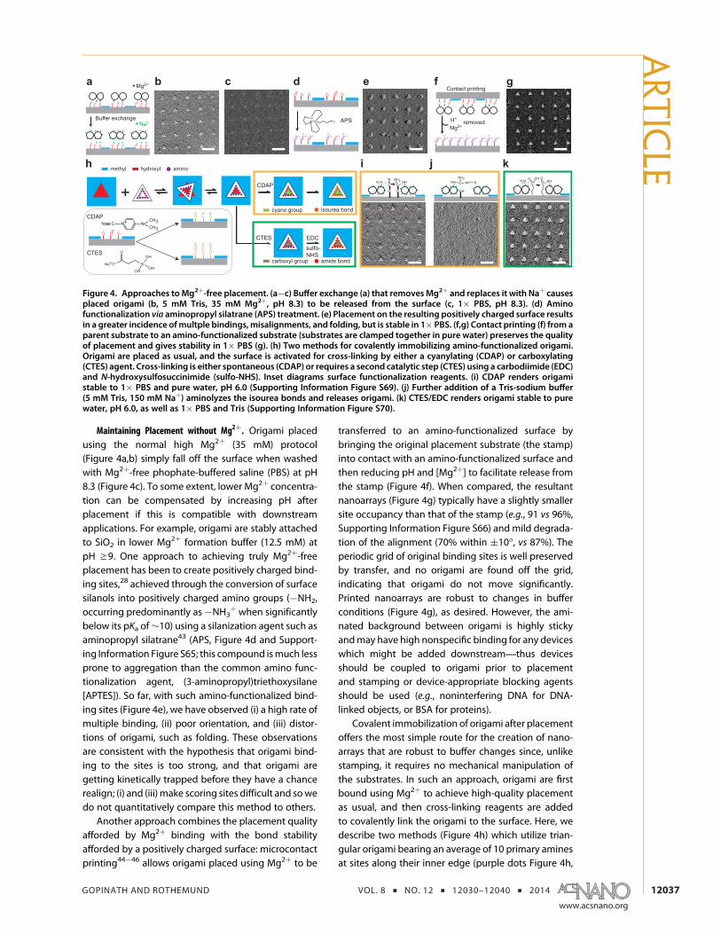
Maintaining Placement without Mg2þ. Origami placedusing the normal high Mg2þ (35 mM) protocol(Figure 4a,b) simply fall off the surface when washedwith Mg2þ-free phophate-buffered saline (PBS) at pH8.3 (Figure 4c). To some extent, lower Mg2þ concentra-tion can be compensated by increasing pH afterplacement if this is compatible with downstreamapplications. For example, origami are stably attachedto SiO2 in lower Mg2þ formation buffer (12.5 mM) atpH g9. One approach to achieving truly Mg2þ-freeplacement has been to create positively charged bind-ing sites,28 achieved through the conversion of surfacesilanols into positively charged amino groups (!NH2,occurring predominantly as!NH3
þ when significantlybelow its pKa of∼10) using a silanization agent such asaminopropyl silatrane43 (APS, Figure 4d and Support-ing Information Figure S65; this compound ismuch lessprone to aggregation than the common amino func-tionalization agent, (3-aminopropyl)triethoxysilane[APTES]). So far, with such amino-functionalized bind-ing sites (Figure 4e), we have observed (i) a high rate ofmultiple binding, (ii) poor orientation, and (iii) distor-tions of origami, such as folding. These observationsare consistent with the hypothesis that origami bind-ing to the sites is too strong, and that origami aregetting kinetically trapped before they have a chancerealign; (i) and (iii) make scoring sites difficult and sowedo not quantitatively compare this method to others.
Another approach combines the placement qualityafforded by Mg2þ binding with the bond stabilityafforded by a positively charged surface: microcontactprinting44!46 allows origami placed using Mg2þ to be
transferred to an amino-functionalized surface bybringing the original placement substrate (the stamp)into contact with an amino-functionalized surface andthen reducing pH and [Mg2þ] to facilitate release fromthe stamp (Figure 4f). When compared, the resultantnanoarrays (Figure 4g) typically have a slightly smallersite occupancy than that of the stamp (e.g., 91 vs 96%,Supporting Information Figure S66) and mild degrada-tion of the alignment (70% within (10!, vs 87%). Theperiodic grid of original binding sites is well preservedby transfer, and no origami are found off the grid,indicating that origami do not move significantly.Printed nanoarrays are robust to changes in bufferconditions (Figure 4g), as desired. However, the ami-nated background between origami is highly stickyandmay have high nonspecific binding for any deviceswhich might be added downstream;thus devicesshould be coupled to origami prior to placementand stamping or device-appropriate blocking agentsshould be used (e.g., noninterfering DNA for DNA-linked objects, or BSA for proteins).
Covalent immobilization of origami after placementoffers the most simple route for the creation of nano-arrays that are robust to buffer changes since, unlikestamping, it requires no mechanical manipulation ofthe substrates. In such an approach, origami are firstbound using Mg2þ to achieve high-quality placementas usual, and then cross-linking reagents are addedto covalently link the origami to the surface. Here, wedescribe two methods (Figure 4h) which utilize trian-gular origami bearing an average of 10 primary aminesat sites along their inner edge (purple dots Figure 4h,
Figure 4. Approaches to Mg2þ-free placement. (a!c) Buffer exchange (a) that removesMg2þ and replaces it with Naþ causesplaced origami (b, 5 mM Tris, 35 mM Mg2þ, pH 8.3) to be released from the surface (c, 1# PBS, pH 8.3). (d) Aminofunctionalization via aminopropyl silatrane (APS) treatment. (e) Placement on the resulting positively charged surface resultsin a greater incidence ofmultple bindings, misalignments, and folding, but is stable in 1# PBS. (f,g) Contact printing (f) from aparent substrate to an amino-functionalized substrate (substrates are clamped together in pure water) preserves the qualityof placement and gives stability in 1# PBS (g). (h) Two methods for covalently immobilizing amino-functionalized origami.Origami are placed as usual, and the surface is activated for cross-linking by either a cyanylating (CDAP) or carboxylating(CTES) agent. Cross-linking is either spontaneous (CDAP) or requires a second catalytic step (CTES) using a carbodiimide (EDC)and N-hydroxysulfosuccinimide (sulfo-NHS). Inset diagrams surface functionalization reagents. (i) CDAP renders origamistable to 1# PBS and pure water, pH 6.0 (Supporting Information Figure S69). (j) Further addition of a Tris-sodium buffer(5 mM Tris, 150 mM Naþ) aminolyzes the isourea bonds and releases origami. (k) CTES/EDC renders origami stable to purewater, pH 6.0, as well as 1# PBS and Tris (Supporting Information Figure S70).
ARTIC
LE

GOPINATH AND ROTHEMUND VOL. 8 ’ NO. 12 ’ 12030–12040 ’ 2014
www.acsnano.org
12038
red dots Supporting Information Figure S67). In thefirst method (Figure 4h, orange box), surface silanolsare converted into cyano groups using 1-cyano(4-dimethylamino)pyridinium tetrafluoroborate (CDAP)in a coupling solution created by mixing acetonitrile50% (v/v) with 5 mM MOPS buffer containing 250 mMMg2þ at pH 7.0. Coupling solution is applied for just10 min to a chip cooled on ice; a pH of 7.0 is used toincrease CDAP activity, and elevated [Mg2þ] (150 mMafter mixing onto the chip) is used to fix origami stablyon the surface at this lower pH. As soon as the cyanogroup is created, it can spontaneously react with anamino-functionalized origami to form an isourea bond.The isourea derivative so formed is susceptible amino-lysis by primary amines.47 This is why MOPS bufferis used for the coupling reaction rather than buffercontaining the amino-bearing Tris base, and this sus-ceptibility enables us to confirm the isourea bond'srole in origami immobilization: postcoupling, we firstimaged origami in PBS buffer (150 mM Naþ, pH 8.3) todemonstrate that they are stable (for at least an hour)under Mg2þ-free conditions (Figure 4i and SupportingInformation Figure 68), consistent with the formationof covalent isourea bonds. We next imaged the sampleunder similar conditions in a buffer that contains 5 mMTris (150 mM Naþ, pH 8.3) and observed that theorigami were completely removed from the surface(Figure 4j).
In a second covalent approach (Figure 4h, blackbox), carboxyl groups are used to cross-link amino-functionalized origami to the surface using EDC[1-ethyl-3-(3-(dimethylamino)propyl)carbodiimide]catalysis.47 After standard Mg2þ-mediated placement,surface silanols were converted to carboxyl groupsby incubating the substrate in a 0.01% (v/v) CTES(carboxyethylsilanetriol) solution. In a second step,carboxyl groups were cross-linked to amino-functiona-lized origami by incubating the substrate in a couplingbuffer (50 mM EDC, 25 mM sulfo-NHS, in 10 mMMOPS,pH 8.1, 125 mM Mg2þ). The resulting amide bond isstable (for at least 24 h) in PBS buffer, and unlike theisourea bond, it is stable in Tris-containing buffer(Supporting Information Figure 70). In general, theamidebond shouldbe stable to awide variety of buffershaving a pH between 5 and 9.
Both covalent approaches provide for total removalof salts: the CDAP and CTES/EDC procedures bothachieve the stable fixation of origami on substratesunder pure water (freshly preparedMilli-Q, nominal pH
of 6.0) for at least an hour (Supporting InformationFigure 69 and Figure 4k), a condition under whichorigami would otherwise be completely removed fromthe surface. Despite the susceptibility of the isoureabond to aminolysis, the CDAP procedure is muchsimpler, involving a single chemical step and a sig-nificant reduction in the number of buffer washes(16 fewer). The CTES/EDC procedure, on the otherhand, should be used in cases where the substrate willlater be subjected to primary amines (as in the case ofTris buffer), other strong nucleophiles, or high pH.
CONCLUSIONS
Here, we have provided experimental conditions forachieving reproducible, high-quality placement onSi/SiO2 substrates, along with protocols for noncova-lently and covalently stabilized origami nanoarrays un-der Mg2þ-free conditions. By examining the spatialdependence of origami binding, we have revealed thatsurface diffusion plays an important role in the bindingmechanism, one that is crucial to understand for creatingnanoarrays of different spacings. With these advances,origami placement should now be widely availablefor nanotechnological and biophysical applicationsin a variety of microfabricated devices;deterministicpositioning an individual receptor in the heart of aphotonic biosensor or a single ligand at the exact endof an AFM tip.The ability to position individual molecules may
also open new doors in chemistry. Origami have beenpreviously used to organize individual reactive chemi-cal groups with ∼5 nm precision13;each origamiserves as an independent nanoscopic reference frameand provides a 100 nm # 70 nm field in which single-molecule reactions can be positioned. Uniquely, ourwork has used directed self-assembly to deliver indivi-dual reactive chemical groups;amines along theinner triangle of the origami;to precise positionson a macroscopic surface, in the laboratory frameof reference. Here the amines were positioned in theservice of covalently coupling origami to the surface,but this need not be the case. Looking forward, one canenvision uses of placementwherein origami aremerelya shuttle, escorting molecular cargo into position forcovalent coupling and then departing, leaving behindsingle molecules precisely located with respect to thelaboratory frame;iterative applications of placementmight underlie a new type of synthesis with exquisitepositional control.
MATERIALS AND METHODSOrigami Formation and Purification. A variation of the “sharp
triangle” design described previously2 was chosen becauseof its rigidity and low tendency to aggregate. Staple strands(Integrated DNA Technologies, 100 μM each in water) and the
scaffold strand (single-stranded M13mp18, Bayou Biolabs,P-107) were mixed together to target concentrations of 100and 40 nM, respectively (a 2.5:1 staple/scaffold ratio) in 10 mMTris base, 1 mM EDTA buffer (adjusted to to pH 8.35 with HCl)with 12.5 mM MgCl2. Next, 50 μL volumes of staple/scaffoldmixture were heated to 90 !C for 5 min and annealed from
ARTIC
LE

GOPINATH AND ROTHEMUND VOL. 8 ’ NO. 12 ’ 12030–12040 ’ 2014
www.acsnano.org
12039
90 to 20 !C at!0.2 !C/min in a PCR machine. DNA LoBind tubes(Eppendorf) (0.5 mL) were used to minimize loss of origami.Amine-functionalized origami were prepared by replacing sta-ples on the inner edge of the triangle with staples extendedby 18-base poly-T linkers, to which a 21-base poly-A strandsbearing 30 amine modifications were hybridized. Origami werepurified using 100 kDa MWCO spin filters (YM-100, Millipore orAmicon Ultra-0.5 filters with Ultracel-100 membranes).
Fabrication of Placement Substrates. Si (for e-beam) or single-crystal quartz (for nanoimprinting) wafers were purchased fromUniversity Wafers. Si wafers were RCA cleaned, immersed in20 wt % HF (aqueous) for 30 s, immersed in 40 wt % NH4F(aqueous) for 60 s, washed in deionized water, and baked ina Tystar Tytan furnace at 1000 !C for 3.25 h. This generateda 100 nm thick SiO2 layer, as verified by a Filmetrics F40 thin-filmanalyzer. Quartz wafers were cleaned with isopropyl alcoholand blown dry with N2. Next, both wafer types were coatedwith trimethylsilyl groups by vapor deposition of HMDS(hexamethyldisilazane). A thin (170!180 nm) layer of poly-(methyl methacrylate) diluted in anisole (PMMA 950 A3,Microchem) was spin-coated on the substrate (2500 rpm for90 s) and baked (at 180 !C for 30 s) for use as a resist duringe-beam lithography or nanoimprinting. E-beam was performedwith a 100 keV beam delivering a dose of 900 μC/cm2 at 700 pA,and the resist was developed with a 1:3 solution of methylisobutyl ketone/isopropyl alcohol (70 s). For nanolithography,a separately fabricated SiO2 mold was cleaned with isopropylalcohol and O2 plasma, coated with tridecafluoro-1,1,2,2-tetrahydooctyl-trichorosilane (Gelest) as a mold release agent,and used to pattern quartz substrates with a Nanonex BX-200system (100 !C and 500 psi for 30 min). Wafers were cutinto 1 cm # 1 cm chips, cleaned with IPA, and activated withanO2 etch (PlasmathermDual Chamber 720/720RIE) at 50 sccm,50 mTorr, and 80 W power for 15 s. Resist was strippedby sonicating chips in n-methyl pyrrolidone (NMP) at 50 !Cfor 10 min.
Placement Protocol. Origami were diluted to 110 pM in place-ment buffer (5mM Tris, pH 8.35, 35mMMg2þ), and a 20 μL dropwas deposited in the middle of a chip. Chips were placed in aclosed 50 mm Petri dish with a moistened kimwipe for 60 min.Origami concentration, incubation time, and buffer pH and[Mg2þ] were changed as desired for optimization purposes.After incubation, excess origami were washed away (8#, 60 μLeach wash, pipetting up and down 2!3 times per wash) takingcare not to dewet the sample. Chips were next washed 5# intoTween washing buffer (5 mM Tris, pH 8.35, 35 mM Mg2þ, 0.1%Tween 20) and incubated for 30 min to remove weakly boundorigami. To remove Tween 20, the chip is washed 8# into higherpH imaging buffer (5 mM Tris, pH 8.9, 30 mM Mg2þ).
AFM Imaging and Analysis. Unless otherwise specified, imageswere taken in solution tapping mode with a Dimension IconAFM/Nanoscope V Scanner (Bruker) using the short, fat canti-lever from an SNL probe (“sharp nitride lever”, 2 nm tip radius,Bruker) resonating at 16!19 kHz. Unless otherwise specified,images are phase images: after engaging, amplitude set pointwas increased until origami were visible only in the phasechannel. This reduced tip!sample interaction. Image wereprocessed using Gwyddion (http://gwyddion.net/).
Microcontact Printing. Origami were placed on SiO2 (42.5 mMMg2þ, pH 8.35, 110 pM origami, 5 mM Tris, 60 min incubation),and the chip was dried via an ethanol series (10 s in each of 25,50, 70, 80, and 90% ethanol followed by air drying) to create a“master”. A second unpatterned SiO2 substrate (the “copy”) wasactivated with O2 plasma, incubated with 0.1% APS in water for20 min, sonicated in DI water, and dried. Master and copy wereclamped together, face to face, and immersed in (1) 10 mMphosphate buffer, pH 7.2 for 5 min and (2) DI water for 30 min.At the end of (2), chips were separated while still under waterand the copy was imaged under 1# PBS buffer.
CDAP Coupling. After optimized placement, chips were bufferwashed (8#, 60 μL each wash, leaving a final 20 μL drop) intoMOPS!Mg2þbuffer (5mMMOPS buffer, 250mMMgCl2, pH 7.0)and put into a Petri dish on ice to cool for 10 min. CDAP (Sigma-Aldrich) solution (250 mg CDAP in 1.5 mL of MOPS!Mg2þ)was prepared fresh. Sixty microliters of coupling solution
(50% acetonitrile, 50% CDAP solution v/v) was pipetted ontothe chip and incubated for 10 min on ice.
CTES/EDC Coupling. CTES (Gelest) stock solution (1% CTES inwater) was used to prepare CTES silanization buffer (0.01% CTESin 10 mM Tris, 35 mM Mg2þ, pH 8.3) fresh for each experiment.After optimized placement, chips were (1) washed into CTESsilanization buffer (8#, 60 μL each wash) and incubated for2 min, (2) washed 8# to remove CTES (10 mM MOPS, 125 mMMg2þ, pH 8.1), and (3) washed into coupling buffer (50mM EDC,25 mM sulfo-NHS, in 10 mM MOPS, pH 8.1, 125 mM Mg2þ) andincubated for 10 min.
Conflict of Interest: The authors declare no competingfinancial interest.
Acknowledgment. We acknowledge financial support fromthe Army Research Office award W911NF-11-1-0117 and theU.S. National Science Foundation for Expeditions in Computingfunding for the Molecular Programming Project (Nos. 0832824and 1317694, http://molecular-programming.org) and Office ofNaval Research Award N000141410702. We acknowledge thegift of aminopropyl silatrane from G. Lovely. We thank S. Guoof Bruker Nano Surfaces for fast scan AFM movies. We thankD. Fygenson, J. Sorensen, T. del Bonis-O'Donnell, S. Woo, andmembers of Winfree lab for discussions. E-beam lithographywas performed in the Kavli Nanoscience Institute at Caltech;nanoimprinting was performed in the UCSB NanofabricationFacility.
Supporting Information Available: More detailed methods,a troubleshooting guide for placement, origami sequence, anddesign files, Supplementary Figures 1!70 and SupplementaryMovies 1!4 provide additional information regarding theresults described throughout the main text. This material isavailable free of charge via the Internet at http://pubs.acs.org.
REFERENCES AND NOTES1. Seeman, N. C. Nucleic Acid Junctions and Lattices. J. Theor.
Biol. 1982, 99, 237–247.2. Rothemund, P. W. K. Folding DNA To Create Nanoscale
Shapes and Patterns. Nature 2006, 440, 297–302.3. Douglas, S. M.; Dietz, H.; Liedl, T.; Högberg, B.; Graf, F.;
Shih, W. M. Self-Assembly of DNA into Nanoscale Three-Dimensional Shapes. Nature 2009, 459, 414–418.
4. Dietz, H.; Douglas, S. M.; Shih, W. M. Folding DNA intoTwisted and Curved Nanoscale Shapes. Science 2009, 325,725–730.
5. Han, D.; Pal, S.; Nangreave, J.; Deng, Z.; Liu, Y.; Yan, H. DNAOrigami with Complex Curvatures in Three-DimensionalSpace. Science 2011, 332, 342–346.
6. Maune, H. T.; Han, S.-P.; Barish, R. D.; Bockrath, M.; Goddard,W. A., III; Rothemund, P. W. K.; Winfree, E. Self-Assemblyof Carbon Nanotubes into Two-Dimensional GeometriesUsing DNA Origami Templates. Nat. Nanotechnol. 2010, 5,61–66.
7. Geng, Y.; Pearson, A. C.; Gates, E. P.; Uprety, B.; Davis, R. C.;Harb, J. N.; Woolley, A. T. Electrically Conductive Gold- andCopper-Metallized DNAOrigami Nanostructures. Langmuir2013, 29, 3482–3490.
8. Ding, B.; Deng, Z.; Yan, H.; Cabrini, S.; Zuckerman, R. N.;Bokor, J. Gold Nanoparticle Self-Similar Chain StructureOrganized by DNA Origami. J. Am. Chem. Soc. 2010, 132,3248–3249.
9. Dutta, P. K.; Varghese, R.; Nangreave, J.; Lin, S.; Yan, H.; Liu,Y. DNA-Directed Artificial Light-Harvesting Antenna. J. Am.Chem. Soc. 2011, 133, 11985–11993.
10. Ko, S. H.; Gallatin, G. M.; Liddle, J. A. Nanomanufacturingwith DNAOrigami: Factors Affecting the Kinetics and Yieldof Quantum Dot Binding. Adv. Funct. Mater. 2012, 22,1015–1023.
11. Kuzyk, A.; Schreiber, R.; Fan, Z.; Pardatscher, G.; Roller, E.-M.;Högele, A.; Simmel, F. C.; Govorov, A. O.; Liedl, T. DNA-Based Self-Assembly of Chiral Plasmonic Nanostructureswith Tailored Optical Response. Nature 2012, 483, 311–314.
ARTIC
LE

GOPINATH AND ROTHEMUND VOL. 8 ’ NO. 12 ’ 12030–12040 ’ 2014
www.acsnano.org
12040
12. Acuna, G. P.; Möller, F. M.; Holzmeister, P.; Beater, S.;Lalkens, B.; Tinnefeld, P. Fluorescence Enhancement atDocking Sites of DNA-Directed Self-Assembled Nano-antennas. Science 2012, 338, 506–510.
13. Voigt, N. V.; Tørring, T.; Rotaru, A.; Jacobsen, M. F.;Ravnsbæk, J. B.; Subramani, R.; Mamdouh, W.; Kjems, J.;Mokhir, A.; Besenbacher, F.; Gothelf, K. V. Single-MoleculeChemical Reactions on DNA Origami. Nat. Nanotechnol.2010, 5, 200–203.
14. Prinz, J.; Schreiber, B.; Olejko, L.; Oertel, J.; Rackwitz, J.;Keller, A.; Bald, I. DNA Origami Substrates for HighlySensitive Surface-EnhancedRaman Scattering. J. Phys. Chem.Lett. 2013, 4, 4140–4145.
15. Thacker, V. V.; Herrmann, L. O.; Sigle, D. O.; Zhang, T.; Liedl,T.; Baumberg, J. J.; Keyser, U. F. DNA Origami BasedAssembly of Gold Nanoparticle Dimers for Surface-Enhanced Raman Scattering. Nat. Commun. 2014, 5, 3448.
16. Rajendran, A.; Endo, M.; Sugiyama, H. Single-MoleculeAnalysis Using DNA Origami. Angew. Chem., Int. Ed. 2012,51, 874–890.
17. Qiu,W.; Derr, N. D.; Goodman, B. S.; Villa, E.; Wu, D.; Shih, W.;Reck-Peterson, S. L. Dynein Achieves Processive MotionUsing Both Stochastic and Coordinated Stepping. Nat.Struct. Mol. Biol. 2012, 19, 193–200.
18. Pfitzner, E.; Wachauf, C.; Kilchherr, F.; Pelz, B.; Shih, W. M.;Rief, M.; Dietz, H. Rigid DNA Beams for High-ResolutionSingle-Molecule Mechanics. Angew. Chem., Int. Ed. 2013,125, 7920–7925.
19. Schreiber, R.; Kempter, S.; Holler, S.; Schüller, V.; Schiffels,D.; Simmel, S. S.; Nickels, P. C.; Liedl, T. DNA Origami-Templated Growth of Arbitrarily Shaped Metal Nano-particles. Small 2011, 7, 1795–1799.
20. Surwade, S. P.; Zhou, F.; Wei, B.; Sun, W.; Powell, A.;O'Donnell, C.; Yin, P.; Liu, H. Nanoscale Growth and Pat-terning of Inorganic Oxides Using DNA NanostructureTemplates. J. Am. Chem. Soc. 2013, 135, 6778–6781.
21. Surwade, S. P.; Zhao, S.; Liu, H. Molecular Lithographythrough DNA-Mediated Etching and Masking of SiO2.J. Am. Chem. Soc. 2011, 133, 11868–11871.
22. Jin, Z.; Sun, W.; Ke, Y.; Shih, C.-J.; Paulus, G. L. C.; Hua Wang,Q.; Mu, B.; Yin, P.; Strano, M. S. Metallized DNA Nanolitho-graphy for Encoding and Transferring Spatial Informationfor Graphene Patterning. Nat. Commun. 2013, 4, 1663.
23. Holloway, C.; Kuester, E. F.; Gordon, J.; O'Hara, J.; Booth, J.;Smith, D. An Overview of the Theory and Applications ofMetasurfaces: the Two-Dimensional Equivalents of Meta-materials. IEEE Antennas Propag. Mag. 2012, 54, 10–35.
24. Kuzyk, A.; Yurke, B.; Toppari, J. J.; Linko, V.; Törmä, P.Dielectrophoretic Trapping of DNA Origami. Small 2008,4, 447–450.
25. Kershner, R. J.; Bozano, L. D.; Micheel, C. M.; Hung, A. M.;Fornof, A. R.; Cha, J. N.; Rettner, C. T.; Bersani, M.; Frommer,J.; Rothemund, P. W. K.; et al. Placement and Orientationof Individual DNA Shapes on Lithographically PatternedSurfaces. Nat. Nanotechnol. 2009, 4, 557–561.
26. Gerdon, A. E.; Oh, S. S.; Hsieh, K.; Ke, Y.; Yan, H.; Soh, H. T.Controlled Delivery of DNAOrigami on Patterned Surfaces.Small 2009, 5, 1942–1946.
27. Hung, A. M.; Micheel, C. M.; Bozano, L. D.; Osterbur, L. W.;Wallraff, G. M.; Cha, J. N. Large-Area Spatially OrderedArrays of Gold Nanoparticles Directed by LithographicallyConfined DNA Origami. Nat. Nanotechnol. 2010, 5, 121–126.
28. Gao, B.; Sarveswaran, K.; Bernstein, G. H.; Lieberman, M.Guided Deposition of Individual DNA Nanostructures onSilicon Substrates. Langmuir 2010, 26, 12680–12683.
29. Ding, B.; Wu, H.; Xu, W.; Zhao, Z.; Liu, Y.; Yu, H.; Yan, H.Interconnecting Gold Islands with DNA Origami Nano-tubes. Nano Lett. 2010, 10, 5065–5069.
30. Pearson, A. C.; Pound, E.; Woolley, A. T.; Linford, M. R.; Harb,J. N.; Davis, R. C. Chemical Alignment of DNA Origami ToBlock Copolymer Patterned Arrays of 5 nm Gold Nano-particles. Nano Lett. 2011, 11, 1981–1987.
31. Penzo, E.; Wang, R.; Palma, M.; Wind, S. J. Selective Place-ment of DNA Origami on Substrates Patterned by
Nanoimprint Lithography. J. Vac. Sci. Technol., B 2011,29, 06F205.
32. Scheible, M. B.; Pardatscher, G.; Kuzyk, A.; Simmel, F. C.Single Molecule Characterization of DNA Binding andStrand Displacement Reactions on Lithographic DNAOrigami Microarrays. Nano Lett. 2014, 14, 1627–1633.
33. Teshome, B.; Facsko, S.; Keller, A. Topography-ControlledAlignment of DNA Origami Nanotubes on NanopatternedSurfaces. Nanoscale 2014, 6, 1790–1796.
34. Dong, Y.; Pappu, S. V.; Xu, Z. Detection of Local DensityDistribution of Isolated Silanol Groups on Planar SilicaSurfaces Using Nonlinear Optical Molecular Probes. Anal.Chem. 1998, 70, 4730–4735.
35. Dishon, M.; Zohar, O.; Sivan, U. Effect of Cation Size andCharge on the Interaction between Silica Surfaces in 1:1,2:1, and 3:1 Aqueous Electrolytes. Langmuir 2011, 27,12977–12984.
36. Cheng, H.; Zhang, K.; Libera, J. A.; Olvera de La Cruz, M.;Bedzyk, M. J. Polynucleotide Adsorption to NegativelyCharged Surfaces in Divalent Salt Solutions. Biophys. J.2006, 90, 1164–1174.
37. Libera, J. A.; Cheng, H.; Olvera de la Cruz, M.; Bedzyk, M. J.Direct Observation of Cations and PolynucleotidesExplains Polyion Adsorption to Like-Charged Surfaces.J. Phys. Chem. B 2005, 109, 23001–23007.
38. Becker, J.; Pysch, D.; Leimenstoll, A.; Hermle, M.; Glunz, S.Wet-Chemical Pre-treatment of c-Si Substrates Enhancingthe Performance of a-Si: H/c-Si Hetero-Junction Solar Cells.24th European PV Solar Energy Conference and Exhibition,Hamburg, Germany. 2009.
39. Pastré, D.; Piétrement, O.; Fusil, S.; Landousy, F.; Jeusset, J.;David, M.-O.; Hamon, L.; Cam, E. L.; Zozime, A. Adsorptionof DNA to Mica Mediated by Divalent Counterions: ATheoretical and Experimental Study. Biophys. J. 2003, 85,2507–2518.
40. Kastantin, M.; Schwartz, D. K. DNA Hairpin Stabilization ona Hydrophobic Surface. Small 2013, 9, 933–941.
41. Skaug, M. J.; Mabry, J.; Schwartz, D. K. Intermittent Molec-ular Hopping at the Solid!Liquid Interface. Phys. Rev. Lett.2013, 110, 256101.
42. Wang, D.; Gou, S.-Y.; Axelrod, D. Reaction Rate Enhance-ment by Surface Diffusion of Adsorbates. Biophys. Chem.1992, 43, 117–137.
43. Shlyakhtenko, L. S.; Gall, A. A.; Filonov, A.; Cerovac, Z.;Lushnikov, A.; Lyubchenko, Y. L. Silatrane-Based SurfaceChemistry for Immobilization of DNA, Protein!DNA Com-plexes and Other Biological Materials. Ultramicroscopy2003, 97, 279–287.
44. Lange, S. A.; Benes, V.; Kern, D. P.; Hörber, J. H.; Bernard, A.Microcontact Printing of DNA Molecules. Anal. Chem.2004, 76, 1641–1647.
45. Kaufmann, T.; Ravoo, B. J. Stamps, Inks and Substrates:Polymers in Microcontact Printing. Polym. Chem. 2010, 1,371–387.
46. Han, S.-p.; Maune, H. T.; Barish, R. D.; Bockrath, M.; Goddard,W. A., III. DNA-Linker-Induced Surface Assembly of UltraDense Parallel Single Walled Carbon Nanotube Arrays.Nano Lett. 2012, 12, 1129–1135.
47. Janson, J.-C. Protein Purification: Principles, High ResolutionMethods, and Applications; John Wiley & Sons: New York,2012; Vol. 151.
ARTIC
LE
Related Documents