A NSWERS ◆ 1 ANSWERS Chapter 1 SECTION CHECKUPS Section 1–1 The Atom 1. The Bohr model has a central nucleus consisting of protons and neutrons orbited by electrons at varying distances from the nucleus. 2. An electron is the smallest particle of negative electrical charge. 3. Protons and neutrons. A proton is a particle of positive charge and a neutron has no net charge. 4. The atomic number is the number of electrons in the nucleus of an atom. 5. An electron shell contains orbiting electrons at a certain energy level. Each shell of a given atom is at a different energy level. 6. A valence electron is one that is in the outer shell of an atom. 7. A free electron is a valence electron that has broken free of its parent atom. 8. A positive ion is a previously neutral atom that has lost a valence electron and has a net positive charge. A negative ion is one that has gained an extra electron and has a net negative charge. 9. The quantum model is based on the uncertainty principle and wave-particle duality. Section 1–2 Materials Used in Electronics 1. Conductors have many free electrons and easily conduct current. Insulators have essentially no free electrons and do not conduct current. 2. Semiconductors do not conduct current as well as conductors do. In terms of conductivity, they are between conductors and insulators. 3. Conductors such as copper have one valence electron. 4. Semiconductors have four valence electrons. 5. Gold, silver, and copper are the best conductors. 6. Silicon is the most widely used semiconductor. 7. The valence electrons of a semiconductor are more tightly bound to the atom than those of conductors. 8. Covalent bonds are formed by the sharing of valence electrons with neighboring atoms. 9. An intrinsic material is one that is in a pure state. 10. A crystal is a solid material formed by atoms bonding together in a symmetrical pattern. Section 1–3 Current in Semiconductors 1. Free electrons are in the conduction band. 2. Free (conduction) electrons are responsible for electron current in silicon. 3. A hole is the absence of an electron in the valence band. 4. Hole current occurs at the valence level. Section 1–4 N-Type and P-Type Semiconductors 1. Doping is the process of adding impurity atoms to a semiconductor in order to modify its con- ductive properties. 2. A pentavalent atom has five valence electrons and a trivalent atom has three valence electrons. 3. A pentavalent atom is called a donor atom and a trivalent atom is called an acceptor atom. 4. An n-type material is formed by the addition of pentavalent impurity atoms to the intrinsic semiconductive material. 5. A p-type material is formed by the addition of trivalent impurity atoms to the intrinsic semi- conductive material. 6. The majority carrier in an n-type semiconductor is the free electron. 7. The majority carrier in a p-type semiconductor is the hole.

Welcome message from author
This document is posted to help you gain knowledge. Please leave a comment to let me know what you think about it! Share it to your friends and learn new things together.
Transcript
ANSWERS ◆ 1
ANSWERS Chapter 1
SECTION CHECKUPSSection 1–1 The Atom
1. The Bohr model has a central nucleus consisting of protons and neutrons orbited by electronsat varying distances from the nucleus.
2. An electron is the smallest particle of negative electrical charge.
3. Protons and neutrons. A proton is a particle of positive charge and a neutron has no net charge.
4. The atomic number is the number of electrons in the nucleus of an atom.
5. An electron shell contains orbiting electrons at a certain energy level. Each shell of a givenatom is at a different energy level.
6. A valence electron is one that is in the outer shell of an atom.
7. A free electron is a valence electron that has broken free of its parent atom.
8. A positive ion is a previously neutral atom that has lost a valence electron and has a netpositive charge. A negative ion is one that has gained an extra electron and has a net negativecharge.
9. The quantum model is based on the uncertainty principle and wave-particle duality.
Section 1–2 Materials Used in Electronics
1. Conductors have many free electrons and easily conduct current. Insulators have essentially nofree electrons and do not conduct current.
2. Semiconductors do not conduct current as well as conductors do. In terms of conductivity, theyare between conductors and insulators.
3. Conductors such as copper have one valence electron.
4. Semiconductors have four valence electrons.
5. Gold, silver, and copper are the best conductors.
6. Silicon is the most widely used semiconductor.
7. The valence electrons of a semiconductor are more tightly bound to the atom than those ofconductors.
8. Covalent bonds are formed by the sharing of valence electrons with neighboring atoms.
9. An intrinsic material is one that is in a pure state.
10. A crystal is a solid material formed by atoms bonding together in a symmetrical pattern.
Section 1–3 Current in Semiconductors
1. Free electrons are in the conduction band.
2. Free (conduction) electrons are responsible for electron current in silicon.
3. A hole is the absence of an electron in the valence band.
4. Hole current occurs at the valence level.
Section 1–4 N-Type and P-Type Semiconductors
1. Doping is the process of adding impurity atoms to a semiconductor in order to modify its con-ductive properties.
2. A pentavalent atom has five valence electrons and a trivalent atom has three valenceelectrons.
3. A pentavalent atom is called a donor atom and a trivalent atom is called an acceptor atom.
4. An n-type material is formed by the addition of pentavalent impurity atoms to the intrinsicsemiconductive material.
5. A p-type material is formed by the addition of trivalent impurity atoms to the intrinsic semi-conductive material.
6. The majority carrier in an n-type semiconductor is the free electron.
7. The majority carrier in a p-type semiconductor is the hole.
FLOY9868_09_SE_Answer.qxd 11/30/10 6:11 PM Page 1
2 ◆ ANSWERS
8. Majority carriers are produced by doping.
9. Minority carriers are thermally produced when electron-hole pairs are generated.
10. A pure semiconductor is intrinsic. A doped (impure) semiconductor is extrinsic.
Section 1–5 The PN Junction
1. A pn junction is the boundary between p-type and n-type semiconductors in a diode.
2. Diffusion is the movement of the free electrons (majority carriers) in the n-region across the pnjunction and into the p region.
3. The depletion region is the thin layers of positive and negative ions that exist on both sides ofthe pn junction.
4. The barrier potential is the potential difference of the electric field in the depletion region andis the amount of energy required to move electrons through the depletion region.
5. The barrier potential for a silicon diode is approximately 0.7 V.
6. The barrier potential for a germanium diode is approximately 0.3 V.
RELATED PROBLEM FOR EXAMPLE1–1 1s2
2s2 2p6
3s2 3p6 3d10
4s2 4p2
TRUE/FALSE QUIZ1. F 2. T 3. T 4. F 5. T 6. T 7. F 8. T 9. F
SELF-TEST1. (c) 2. (d) 3. (a) 4. (b) 5. (a) 6. (d) 7. (d) 8. (c)
9. (d) 10. (d) 11. (d) 12. (d) 13. (c) 14. (b) 15. (a) 16. (d)
17. (e) 18. (a) 19. (b) 20. (c) 21. (c) 22. (a) 23. (c) 24. (d)
25. (d)
ANSWERS Chapter 2
SECTION CHECKUPSSection 2–1 Diode Operation
1. When forward-biased, a diode conducts current. The free electrons in the n region move acrossthe pn junction and combine with the holes in the p region.
2. To forward-bias a diode, the positive side of an external bias voltage is applied to the p regionand the negative side to the n region.
3. When reverse-biased, a diode does not conduct current except for an extremely small reversecurrent.
4. To reverse-bias a diode, the positive side of an external bias voltage is applied to the n regionand the negative side to the p region.
5. The depletion region for forward bias is much narrower than for reverse bias.
6. Majority carrier current is produced by forward bias.
7. Reverse current is produced by the minority carriers.
8. Reverse breakdown occurs when the reverse-bias voltage equals or exceeds the breakdownvoltage of the pn junction of a diode.
9. Avalanche effect is the rapid multiplication of current carriers in reverse breakdown.
FLOY9868_09_SE_Answer.qxd 11/30/10 6:11 PM Page 2

ANSWERS ◆ 3
Section 2–2 Voltage-Current Characteristic of a Diode
1. The knee of the characteristic curve in forward bias is the point at which the barrier potential isovercome and the current increases drastically.
2. A forward-biased diode is normally operated above the knee of the curve.
3. Breakdown voltage is always much greater than the barrier potential.
4. A reverse-biased diode is normally operated between 0 V and the breakdown voltage.
5. Barrier potential decreases as temperature increases.
Section 2–3 Diode Models
1. A diode is operated in forward bias and reverse bias.
2. A diode should never be operated in reverse breakdown.
3. The diode can be ideally viewed as a switch.
4. A diode includes barrier potential, dynamic resistance, and reverse resistance in the complete model.
5. The complete diode model is the most accurate diode approximation.
Section 2–4 Half-Wave Rectifiers
1. PIV across the diode occurs at the peak of the input when the diode is reversed biased.
2. There is current through the load for approximately half (50%) of the input cycle.
3. The average value is
4. The peak output voltage is
5. The PIV sating must be at least 60 V.
Section 2–5 Full-Wave Rectifiers
1. A full-wave voltage occurs on each half of the input cycle and has a frequency of twice theinput frequency. A half-wave voltage occurs once each input cycle and has a frequency equal tothe input frequency.
2. The average value of
3. The bridge rectifier has the greater output voltage.
4. The 50 V diodes must be used in the bridge rectifier.
5. In the center-tapped rectifier, diodes with a PIV rating of at least 90 V would be required.
Section 2–6 Power Supply Filters and Regulators
1. The output frequency is 60 Hz.
2. The output frequency is 120 Hz.
3. The ripple voltage is caused by the slight charging and discharging of the capacitor through theload resistor.
4. The ripple voltage amplitude increases when the load resistance decreases.
5. Ripple factor is the ratio of the ripple voltage to the average or dc voltage.
6. Input regulation is a measure of the variation in output voltage over a range of input voltages.Load regulation is a measure of the variation in output voltage over a range of load current values.
Section 2–7 Diode Limiters and Clampers
1. Limiters clip off or remove portions of a waveform. Clampers insert a dc level.
2. A positive limiter clips off positive voltages. A negative limiter clips off negative voltages.
3. 0.7 V appears across the diode.
4. The bias voltage must be
5. The capacitor acts as a battery.
Section 2–8 Voltage Multipliers
1. The peak voltage rating must be 100 V.
2. The PIV rating must be at least 310 V.
5 V - 0.7 V = 4.3 V.
2(60 V)>p = 38.12 V
25 V - 0.7 V = 24.3 V.
10 V>p = 3.18 V.
FLOY9868_09_SE_Answer.qxd 11/30/10 6:11 PM Page 3
4 ◆ ANSWERS
Section 2–9 The Diode Datasheet
1. 1N4002: 100 V; 1N4003: 200 V; 1N4004: 400 V; 1N4005: 600 V; 1N4006: 800 V
2. No
3. Approximately 0.65 A
4. 12 A
Section 2–10 Troubleshooting
1. 0.5 V to 0.9 V
2. OL
3. An open diode results in no output voltage.
4. An open diode produces a half-wave output voltage.
5. The shorted diode may burn open. Transformer will be damaged. Fuse will blow.
6. The amplitude of the ripple voltage increases with a leaky filter capacitor.
7. There will be no output voltage when the primary opens.
8. The problem may be a partially shorted secondary winding.
RELATED PROBLEMS FOR EXAMPLES2–1 VD 5 V; VLIMIT 0 V
2–2 3.82 V
2–3 (a) 2.3 V (b) 49.3 V
2–4 (a) 623.3 V (b) 624 V (c) negative half-cycles rather than positive half cycles
2–5 98.7 V
2–6 79.3 V including diode drop
2–7 41.0 V; 41.7 V
2–8 26.9 mV
2–9 3.7%
2–10 A positive peak of 9.9 V and clipped at
2–11 Limited at +10.7 V and
2–12 Change R3 to or R2 to
2–13 Same voltage waveform as Figure 2–66
2–14 Verify C is shorted and replace it.
TRUE/FALSE QUIZ1. F 2. F 3. T 4. F 5. T 6. T 7. F 8. T 9. F
10. F 11. T 12. T 13. T 14. F 15. T 16. F 17. F 18. T
19. F 20. T
CIRCUIT-ACTION QUIZ1. (a) 2. (c) 3. (c) 4. (a) 5. (a) 6. (c) 7. (b) 8. (a)
9. (a) 10. (b) 11. (c) 12. (c) 13. (b) 14. (a) 15. (a) 16. (c)
17. (b) 18. (c) 19. (b) 20. (a)
SELF-TEST1. (c) 2. (d) 3. (d) 4. (b) 5. (b) 6. (b) 7. (d) 8. (b)
9. (a) 10. (c) 11. (a) 12. (d) 13. (a) 14. (c) 15. (d) 16. (a)
17. (b) 18. (a) 19. (d) 20. (b) 21. (c) 22. (a) 23. (b) 24. (c)
25. (a) 26. (d) 27. (b) 28. (d) 29. (c) 30. (b) 31. (a) 32. (b)
33. (c) 34. (b) 35. (a) 36. (c) 37. (b)
220 Æ.100 Æ
-10.7 V
-0.7 V
==
FLOY9868_09_SE_Answer.qxd 11/30/10 6:11 PM Page 4
ANSWERS ◆ 5
ANSWERS Chapter 3
SECTION CHECKUPSSection 3–1 The Zener Diode
1. Zener diodes are operated in the reverse-breakdown region.
2. The test current, IZ
3. The zener impedance causes the voltage to vary slightly with current.
4. The zener voltage increases (or decreases) 0.05% for each degree centigrade increase (ordecrease).
5. Power derating is the reduction in the power rating of a device as a result of an increase intemperature.
Section 3–2 Zener Diode Applications
1. An infinite resistance (open)
2. With no load, there is no current to a load. With full load, there is maximum current to the load.
3. Approximately 0.7 V, just like a rectifier diode
Section 3–3 The Varactor Diode
1. A varactor exhibits variable capacitance.
2. A varactor is operated in reverse bias.
3. The depletion region
4. Capacitance decreases with more reverse bias.
5. The capacitance ratio is the ratio of a varactor’s capacitance at a specified minimum voltage tothe capacitance at a specified maximum voltage.
Section 3–4 Optical Diodes
1. Infrared and visible light
2. Infrared has the greater wavelength.
3. An LED operates in forward bias.
4. Light emission increases with forward current.
5. False, VF of an LED is usually greater than 1.2 V.
6. A tiny grouping of red, green, and blue LEDs.
7. A photodiode operates in reverse bias.
8. The internal resistance decreases.
9. Dark current is the reverse photodiode current when there is no light.
Section 3–5 Other Types of Diodes
1. light amplification by stimulated emission of radiation
2. Coherent light has only a single wavelength, but incoherent light has a wide band of wave-lengths. A laser diode produces coherent light.
3. High-frequency and fast-switching circuits
4. Hot carrier is another name for Schottky diodes.
5. Tunnel diodes have negative resistance.
6. Oscillators
7. p region, n region, and intrinsic (i) region
8. A current regulator operates between VL (limiting voltage) and POV (peak operating voltage).
Section 3–6 Troubleshooting
1. The output voltage is too high and equal to the rectifier output.
2. More
FLOY9868_09_SE_Answer.qxd 11/30/10 6:11 PM Page 5
6 ◆ ANSWERS
3. Series limiting resistor open, fuse blown. A shorted zener could have caused this.
4. The output voltage changes as the load resistance changes.
RELATED PROBLEMS FOR EXAMPLES3–1
3–2 The voltage will decrease by 0.45 V.
3–3 7.5 W
3–4
3–5 VIN(min) = 6.77 V; VIN(max) = 21.9 V
3–6
3–7 (a) 11.8 V at IZK; 12.9 V at IZM
(b)
(c)
3–8 (a) A waveform identical to Figure 3-20(a)
(b) A sine wave with a peak value of 5 V
3–9 Increase V2.
3–10 approximately 0.7
3–11 Sixteen parallel branches with four LEDs in each branch.
3–12 approximately
TRUE/FALSE QUIZ1. T 2. T 3. F 4. F 5. T 6. F
7. T 8. T 9. F 10. T 11. T 12. T
CIRCUIT-ACTION QUIZ1. (c) 2. (b) 3. (a) 4. (a) 5. (b) 6. (c) 7. (c) 8. (b)
9. (a) 10. (a) 11. (b)
SELF-TEST1. (a) 2. (b) 3. (c) 4. (b) 5. (d) 6. (a) 7. (c) 8. (d)
9. (d) 10. (d) 11. (b) 12. (b) 13. (d) 14. (b) 15. (d)
6.6 mA
RLIMIT = (12 V - 9.2 V)>30 mA = 93 Æ.
151 Æ
133 Æ
IL(min) = 0 A; IL(max) = 43 mA; RL(min) = 76.7 Æ
VZ = -11.9 V at 10 mA; VZ = 12.08 V at 30 mA
5 Æ
ANSWERS Chapter 4
SECTION CHECKUPSSection 4–1 Bipolar Junction Transistor (BJT) Structure
1. The two types of BJTs are npn and pnp.
2. The terminals of a BJT are base, collector, and emitter.
3. The three regions of a BJT are separated by two pn junctions.
Section 4–2 Basic BJT Operation
1. To operate as an amplifier, the base-emitter is forward-biased and the base-collector is reverse-biased.
2. The emitter current is the largest.
3. The base current is much smaller than the emitter current.
4. The base region is very narrow compared to the other two regions.
5. IE 1 mA 10 mA 1.01 mA=+=
FLOY9868_09_SE_Answer.qxd 11/30/10 6:11 PM Page 6
ANSWERS ◆ 7
Section 4–3 BJT Characteristics and Parameters
1. bDC IC�IB; aDC IC�IE; hFE is bDC.
2. bDC 100; aDC 100�(100 1) 0.99
3. IC is plotted versus VCE.
4. Forward-reverse bias is required for amplifier operation.
5. bDC increases with temperature.
6. No. bDC generally varies some from one device to the next for a given type.
Section 4–4 The BJT as an Amplifier
1. Amplification is the process where a smaller signal is used to produce a larger identical signal.
2. Voltage gain is the ratio of output voltage to input voltage.
3. RC and determine the voltage gain.
4. Av 5 V�250 mV 20
5. Av 1200 Æ�20 Æ 60
Section 4–5 The BJT as a Switch
1. A transistor switch operates in cutoff and saturation.
2. The collector current is maximum in saturation.
3. The collector current is approximately zero in cutoff.
4. VCE VCC in cutoff.
5. VCE is minimum in saturation.
Section 4–6 The Phototransistor
1. The base current of a phototransistor is light induced.
2. Base
3. The collector current depends on bDC and Il.
4. Current transfer ratio
Section 4–7 Transistor Categories and Packaging
1. Three categories of BJTs are small signal/general purpose, power, and RF.
2. Emitter is the lead closest to the tab.
3. The metal mounting tab or case in power transistors is the collector.
Section 4–8 Troubleshooting
1. First, test it in-circuit.
2. If RB opens, the transistor is in cutoff.
3. The base voltage is +3 V and the collector voltage is +9 V.
RELATED PROBLEMS FOR EXAMPLES4–1 10 mA
4–2 IB 241 mA; IC 21.7 mA; IE 21.94 mA; VCE 4.23 V; VCB 3.53 V
4–3 Along the horizontal axis
4–4 Not saturated
4–5 10 V
4–6 VCC(max) 44.5 V; VCE(max) is exceeded first.
4–7 4.55 W
4–8 PD(max) 500 mW @ 50°C
4–9 2.5 kÆ
=
=
=====
=
==
==
r¿e
=+==
==
FLOY9868_09_SE_Answer.qxd 11/30/10 6:11 PM Page 7
8 ◆ ANSWERS
4–10 78.4 mA
4–11 Reduce RC to 140 Æ and RB to 2.2 kÆ.
4–12 RB open
TRUE/FALSE QUIZ1. T 2. F 3. T 4. T 5. F 6. F
7. F 8. T 9. F 10. T 11. F 12. T
CIRCUIT-ACTION QUIZ1. (a) 2. (a) 3. (c) 4. (b) 5. (c) 6. (b)
7. (c) 8. (a) 9. (b) 10. (a) 11. (a) 12. (a)
SELF-TEST1. (d) 2. (c) 3. (a) 4. (d) 5. (a) 6. (c) 7. (b)
8. (a) 9. (c) 10. (c) 11. (b) 12. (b) 13. (f) 14. (c)
15. (b) 16. (b) 17. (b) 18. (a) 19. (d) 20. (a) 21. (c)
ANSWERS Chapter 5
SECTION CHECKUPSSection 5–1 The DC Operating Point
1. The upper load line limit is IC(sat) and VCE(sat). The lower limit is IC � 0 and VCE(cutoff).
2. The Q-point is the dc point at which a transistor is biased and is specified by VCE and IC.
3. Ideally, saturation occurs at the intersection of the load line and the y-axis (VCE � 0 V). Cutoffoccurs at the intersection of the load line and the IB � 0 curve.
4. The Q-point must be centered on the load line for maximum Vce.
Section 5–2 Voltage-Divider Bias
1.
2.
3. VB � 5 V
4. Voltage-divider bias is stable and requires only one supply voltage.
Section 5–3 Other Bias Methods
1. Emitter bias is much less dependent on the value of beta than is base bias.
2. Emitter bias requires two separate supply voltages.
3. IC increases with causing a reduction in VC and, therefore, less voltage across RB, thusless IB.
4. Base bias is beta-dependent.
5. The Q-point changes due to changes in and VCE over temperature.
6. Emitter-feedback improves stability.
Section 5–4 Troubleshooting
1. A transistor is saturated when VCE � 0 V. A transistor is in cutoff when VCE � VCC.
2. RE is open because the BE junction of the transistor is still forward-biased.
3. If RC is open, VC is about 0.7 V less than VB.
bDC
bDC,
RIN(BASE) = (bDCVB)>IE = [(190)(2 V)]>2 mA = 190 kÆ
RIN(BASE) = VIN>IIN = 5 V>5 mA = 1 MÆ
FLOY9868_09_SE_Answer.qxd 11/30/10 6:11 PM Page 8

ANSWERS ◆ 9
RELATED PROBLEMS FOR EXAMPLES5–1 ICQ � 19.8 mA; VCEQ � 4.2 V;
5–2 The voltage divider would be loaded, so VB would decrease.
5–3
5–4
5–5
5–6 7.83 V
5–7
5–8 10.3 mA
5–9 5.38 mA
5–10
TRUE/FALSE QUIZ1. T 2. F 3. T 4. F 5. T 6. F
7. T 8. T 9. F 10. T 11. T 12. T
CIRCUIT-ACTION QUIZ1. (a) 2. (b) 3. (b) 4. (b) 5. (a)
6. (c) 7. (c) 8. (a) 9. (b) 10. (a)
SELF-TEST1. (b) 2. (c) 3. (d) 4. (d) 5. (c) 6. (a) 7. (b) 8. (d)
9. (a) 10. (c) 11. (c) 12. (a) 13. (c) 14. (f) 15. (b) 16. (d)
ANSWERS Chapter 6
SECTION CHECKUPSSection 6–1 Amplifier Operation
1. Positive, negative
2. VCE is a dc quantity and Vce is an ac quantity.
3. Re is the external emitter ac resistance, is the internal emitter ac resistance.
Section 6–2 Transistor AC Models
1. ac—ac alpha, Ic�Ie; βac—ac beta, Ic�Ib; —ac emitter resistance; —ac base resistance; —ac collector resistor.
2. hfe is equivalent to
3.
Section 6–3 The Common-Emitter Amplifier
1. The capacitors are treated as opens.
2. The gain increases with a bypass capacitor.
3. Swamping eliminates the effects of by partially bypassing RE.
4. Total input resistance includes the bias resistors, and any unbypassed RE.
5. The gain is determined by and any unbypassed RE.
6. The voltage gain decreases with a load.
7. The input and output voltages are out of phase.180°
Rc, r¿e,
r¿e,
r¿e
r¿e = 25 mV>15 mA = 1.67 Æ
bac.
r¿e
r¿br¿ea
r¿e
%¢IC = 8.2%; %¢VCE = -30.7%
IC = 853 mA; VCE = 1.47 V
IC = 1.41 mA; VCE = 9.27 V
bDC = 288
RIN(BASE) = 453 kÆ
92.3 kÆ
Ib( peak) = 42 mA
FLOY9868_09_SE_Answer.qxd 11/30/10 6:11 PM Page 9

10 ◆ ANSWERS
Section 6–4 The Common-Collector Amplifier
1. A common-collector amplifier is an emitter-follower.
2. The maximum voltage gain of a common-collector amplifier is 1.
3. A common-collector amplifier has a high input resistance.
Section 6–5 The Common-Base Amplifier
1. Yes
2. The common-base amplifier has a low input resistance.
3. The maximum current gain is 1 in a CB amplifier.
Section 6–6 Multistage Amplifiers
1. A stage is one amplifier in a cascaded arrangement.
2. The overall voltage gain is the product of the individual gains.
3.
4. At lower frequencies, XC becomes large enough to affect the gain.
Section 6–7 The Differential Amplifier
1. Double-ended differential input is between two input terminals. Single-ended differential inputis from one input terminal to ground (with other input grounded).
2. Common-mode rejection is the ability of an op-amp to produce very little output when thesame signal is applied to both inputs.
3. A higher CMRR results in a lower common-mode gain.
Section 6–8 Troubleshooting
1. If C4 opens, the gain drops. The dc level would not be affected.
2. Q2 would be biased in cutoff.
3. The collector voltage of Q1 and the base, emitter, and collector voltages of Q2 would change.
RELATED PROBLEMS FOR EXAMPLES6–1 IC 5 mA; VCE 1.5 V
6–2 3.13 mA
6–3 9.3 mV
6–4
6–5 97.3
6–6 83
6–7 5; 165
6–8 9.56
6–9 Increases
6–10 71. A single transistor loads the CE amplifier much more than the Darlington pair.
6–11 64.1
6–12
6–13 34,000; 90.6 dB
6–14 C3 open
TRUE/FALSE QUIZ1. T 2. T 3. F 4. T 5. F 6. F 7. T 8. T
9. T 10. F 11. T 12. F 13. T 14. T 15. F
A¿v(db) = 63.52 dBA¿v = 1500; Av1(dB) = 27.96 dB; Av2(dB) = 13.98 dB; Av3(dB) = 21.58 dB;
C2 = 28.4 mF
==
20 log (500) = 54.0 dB
FLOY9868_09_SE_Answer.qxd 11/30/10 6:11 PM Page 10

ANSWERS ◆ 11
CIRCUIT-ACTION QUIZ1. (a) 2. (b) 3. (a) 4. (b) 5. (a) 6. (c) 7. (c) 8. (c)
9. (c) 10. (c)
SELF-TEST1. (a) 2. (b) 3. (c) 4. (b) 5. (a) 6. (b) 7. (b) 8. (d)
9. (d) 10. (d) 11. (d) 12. (c) 13. (a) 14. (c) 15. (a) 16. (d)
17. (b) 18. (a) 19. (c)
ANSWERS Chapter 7
SECTION CHECKUPSSection 7–1 The Class A Power Amplifier
1. To dissipate excessive heat
2. The collector
3. Cutoff and saturation clipping
4. 25%
5. The ratio of input resistance to output resistance
Section 7–2 The Class B and Class AB Push-Pull Amplifiers
1. The class B Q-point is at cutoff.
2. The barrier potential of the base-emitter junction causes crossover distortion.
3. Maximum efficiency of a class B amplifier is 79%.
4. Push-pull reproduces both positive and negative alternations of the input signal with greaterefficiency.
5. Both transistors in class AB are biased slightly above cutoff. In class B they are biased at cutoff.
Section 7–3 The Class C Amplifier
1. Class C is biased well into cutoff.
2. The purpose of the tuned circuit is to produce a sinusoidal voltage output.
3. [1 W (1 W � 0.1 W)]100 � 90.9%
Section 7–4 Troubleshooting
1. Excess input signal voltage
2. Open bypass capacitor, C2
RELATED PROBLEMS FOR EXAMPLES7–1 Power gain increases.
7–2 The efficiency goes up because no power is wasted in RE3. The problem is that the speakerhas direct current in the coil and may burn open.
7–3 15 V, 0.1 A
7–4 7.5 V; 0.25 A
7–5 Pout � 1.76 W; PDC � 2.24 W
7–6 Rin would increase.
7–7 3 mW
7–8 The efficiency decreases.
7–9 Halve the input frequency.
>h =
FLOY9868_09_SE_Answer.qxd 11/30/10 6:11 PM Page 11
12 ◆ ANSWERS
TRUE/FALSE QUIZ1. T 2. T 3. F 4. T 5. F 6. T
7. T 8. F 9. T 10. T 11. F 12. T
CIRCUIT-ACTION QUIZ1. (c) 2. (c) 3. (c) 4. (a) 5. (a)
6. (b) 7. (c) 8. (c) 9. (c) 10. (a)
SELF-TEST1. (a) 2. (b) 3. (b) 4. (a) 5. (b) 6. (c) 7. (a) 8. (e) 9. (c)
10. (c) 11. (a) 12. (c) 13. (b) 14. (d) 15. (a) 16. (d) 17. (c)
ANSWERS Chapter 8
SECTION CHECKUPSSection 8–1 The JFET
1. Drain, source, and gate
2. An n-channel JFET requires a negative VGS.
3. ID is controlled by VGS.
Section 8–2 JFET Characteristics and Parameters
1. When VDS � 7 V at pinch-off and
2. As VGS increases negatively, ID decreases.
3. For VP � �3 V, VGS(off) � �3 V.
Section 8–3 JFET Biasing
1. A p-channel JFET requires a positive VGS.
2.
3.
Section 8–4 The Ohmic Region
1.
2. Channel resistance increases.
3.
Section 8–5 The MOSFET
1. Enhancement MOSFET (E-MOSFET) and depletion MOSFET (D-MOSFET)
2. ID increases.
3. ID decreases.
Section 8–6 MOSFET Characteristics and Parameters
1. The D-MOSFET has a structural channel; the E-MOSFET does not.
2. VGS(th) and K are not specified for D-MOSFETs.
3. ESD is ElectroStatic Discharge.
Section 8–7 MOSFET Biasing
1. When VGS � 0 V, the drain current is equal to IDSS.
2. VGS must exceed VGS(th) � 2 V for conduction to occur.
1176 Æ
2 kÆ
VGS = VG - VS = 3 V - 5 V = -2 V
VGS = VG - VS = 0 V - (8 mA)(1.0 kÆ) = -8 V
VGS = 0 V, VP = -7 V.
FLOY9868_09_SE_Answer.qxd 11/30/10 6:11 PM Page 12
ANSWERS ◆ 13
Section 8–8 The IGBT
1. IGBT stands for insulated-gate bipolar transistor.
2. High-voltage switching applications
3. The IGBT has a lower output saturation voltage than the MOSFET.
4. The IGBT has a very high input resistance compared to a BJT.
5. Latch-up is a condition in which the IGBT is in the on state and cannot be turned off by thegate voltage.
Section 8–9 Troubleshooting
1. RS open, no ground connection
2. Because VGS remains at approximately zero
3. The device is off and VD � VDD.
RELATED PROBLEMS FOR EXAMPLES8–1 ID remains at approximately 12 mA.
8–2
8–3 ID � 3.52 mA
8–4
8–5
8–6
8–7
8– 8
8–9
8–10
8–11
8–12
8–13 ID does not change because of the constant-current source.
8–14 RDS values would not change because slopes are constant.
8–15
8–16 ID � 25 mA
8–17 (a) p channel (b) 6.48 mA (c) 35.3 mA
8–18 VGS � 3.13 V; VDS � 21.4 V
8–19 ID � 2.13 mA
8–20 VDS � 5.6 V
TRUE/FALSE QUIZ1. T 2. F 3. T 4. F 5. F 6. T 7. T
8. F 9. T 10. T 11. F 12. T 13. F 14. T
CIRCUIT-ACTION QUIZ1. (b) 2. (c) 3. (b) 4. (b) 5. (a) 6. (a) 7. (c) 8. (b)
SELF-TEST1. (e) 2. (b) 3. (a) 4. (c) 5. (d) 6. (c) 7. (a) 8. (c)
9. (b) 10. (d) 11. (a) 12. (c) 13. (d) 14. (b) 15. (d) 16. (c)
17. (d) 18. (c) 19. (d) 20. (b) 21. (a) 22. (a) 23. (d) 24. (c)
25. (c)
1.07 kÆ
ID � 1.25 mA, VGS � -2.25 V
ID = 1.81 mA, VGS = -2.44 V
VGS � -1.8 V, ID � 1.8 mA
RS = 294 Æ; RD = 3 kÆ
RS = 889 Æ
RS = 245 Æ
VDS = 2 V; VGS = -3.12 V
RIN = 25,000 MÆ
gm = 1800 mS; ID = 4.32 mA
VP = -4 V
FLOY9868_09_SE_Answer.qxd 11/30/10 6:11 PM Page 13

14 ◆ ANSWERS
ANSWERS Chapter 9
SECTION CHECKUPSSection 9–1 The Common-Source Amplifier
1. The FET with gm � 3.5 mS can produce the higher gain.
2.
3. Id is at its positive peak and Vds is at its negative peak when Vgs is at its positive peak.
4. Vgs is an ac quantity, VGS is a dc quantity.
5. Voltage gain of a CS amplifier is determined by gm and Rd.
6. The gain is halved because Rd � RD 2.
Section 9–2 The Common-Drain Amplifier
1. The ideal maximum voltage gain of a CD amplifier is 1.
2. The voltage gain of a CD amplifier is determined by gm and Rs.
Section 9–3 The Common-Gate Amplifier
1. The CG amplifier has a low input resistance (1 gm).
2. gm affects both voltage gain and input resistance.
3. High input resistance, high gain, and excellent high-frequency response
Section 9–4 The Class D Amplifier
1. Modulator, push-pull switching amplifier, and low-pass filter
2. The pulse width is proportional to the amplitude of the input signal.
3. It is passed through a low-pass filter.
Section 9–5 MOSFET Analog Switching
1. When it is turned off
2. When it is turned on
3. A pulse or dc voltage
4. R depends inversely on frequency and capacitance.
Section 9–6 MOSFET Digital Switching
1. A CMOS inverter consists of a p-channel and an n-channel MOSFET connected in a cascadearrangement.
2. NAND gate
3. NOR gate
Section 9–7 Troubleshooting
1. To be a good troubleshooter, you must understand the circuit.
2. There would be a lower than normal first-stage gain if C2 opens.
3. No, but there would be a loss of signal to the second stage.
RELATED PROBLEMS FOR EXAMPLES9–1 13.2
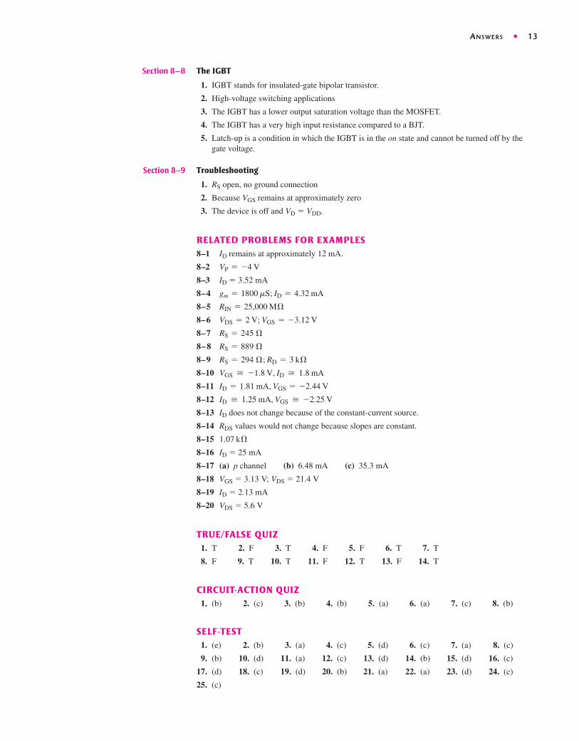
9–2 See Figure ANS9–1.
9–3 2.319 mA
9–4 See Figure ANS9–2.
9–5 350 mV
9–6 Rin = 9.99 MÆ
>
>
Av = gm Rd = (2500 mS)(10 kÆ) = 25
FLOY9868_09_SE_Answer.qxd 11/30/10 6:11 PM Page 14
ANSWERS ◆ 15
9–7 decreases; distortion and clipping at cutoff
9–8 VGS � 2.23 V; ID � 1.09 mA; VDS � 11.4 V; Vout � 750 mV
9–9 0.976
9–10 Rin � 476
9–11 The gain increases.
9–12 0.951
9–13 The MOSFET switch would turn off.
9–14 �
9–15 Same as the input (no inversion)
TRUE/FALSE QUIZ1. T 2. T 3. F 4. F 5. T 6. F 7. F 8. T
9. T 10. F 11. T 12. T 13. T 14. F 15. F
CIRCUIT-ACTION QUIZ1. (a) 2. (b) 3. (a) 4. (c) 5. (a) 6. (b)
7. (b) 8. (c) 9. (b)
SELF-TEST1. (f) 2. (b) 3. (c) 4. (d) 5. (a) 6. (c) 7. (a) 8. (c)
9. (b) 10. (a) 11. (d) 12. (a) 13. (b) 14. (d) 15. (c) 16. (a)
17. (c) 18. (b) 19. (d) 20. (a) 21. (b)
ANSWERS Chapter 10
SECTION CHECKUPSSection 10–1 Basic Concepts
(a) The coupling and bypass capacitors affect the low-frequency gain.
(b) The high-frequency gain is limited by internal capacitances.
(c) Coupling and bypass capacitors can be neglected at frequencies for which their reactances arenegligible.
(d) Cin(Miller) � (5 pF)(51) � 255 pF
(e) Cout(Miller) � (3 pF)(1.04) � 3.12 pF
24 kHz
Æ
¢ID
� ANS9–1 � ANS9–2
5.0
4.0
3.0
2.0
1.0
0−2.0−4.0−6.0
ID (mA)
IDSS
VGS(off)
−VGS (V)−8.0
Q point
5.0
4.0
3.0
2.0
1.0
0−1.0−2.0−3.0
ID (mA)
IDSS
VGS(off)
−VGS (V)−4.0
Q point
FLOY9868_09_SE_Answer.qxd 11/30/10 6:11 PM Page 15

16 ◆ ANSWERS
Section 10–2 The Decibel
(a) �12 dB corresponds to a voltage gain of approximately 4.
(b)
(c) 0 dBm corresponds to 1 mW.
Section 10–3 Low-Frequency Amplifier Response
(a) fcl2 � 167 Hz is dominant.
(b)
(c) attenuation at one decade below fcl.
(d)
(e)
Section 10–4 High-Frequency Amplifier Response
(a) The internal transistor capacitances determine the high-frequency response.
(b) Cin(tot) � Cin(Miller) � Cce � (4 pF)(81) � 8 pF � 342 pF
(c) The input RC circuit dominates.
(d) Ciss and Crss are usually specified on a FET datasheet.
(e) Cin(tot) � (3 pF)(26) � 4 pF � 82 pF
Section 10–5 Total Amplifier Frequency Response
(a) The gain is 1 at fT.
(b)
(c) Av � 130 MHz�50 MHz � 2.6
Section 10–6 Frequency Response of Multistage Amplifiers
(a)
(b)
(c) BW decreases.
Section 10–7 Frequency Response Measurements
(a) fcl � 125 Hz; fcu � 500 kHz
(b) Rise time is between the 10% and 90% points and fall time is between the 90% and 10%points.
(c) tr � 150 ns
(d) tf � 2.8 ms
(e) Since
RELATED PROBLEMS FOR EXAMPLES10–1 (a) 61.6 dB (b) 17 dB (c) 102 dB
10–2 (a) 50 V (b) 6.25 V (c) 1.56 V
10–3
10–4 212 @ 400 Hz; 30 @ 40 Hz; 3 @ 4 Hz
10–5 It will increase the gain and reduce the lower critical frequency.
10–6 C2 “sees” a smaller resistance.
10–7 fcl changes from 16.2 Hz to 16.1 Hz.
10–8 Ideally, the low-frequency response is not affected because an infinite load makes fc of theoutput stage even lower, so the input stage determines the lower cutoff frequency of theamplifier.
10–9 The resistance of the input will be higher, so the critical frequency is lower.
0.22 mF
fcu 77 fcl, BW � fcu = 2.5 MHz.
f ¿cu(dom) = 49 kHz
f ¿cl(dom) = 1 kHz
BW = 25 kHz - 100 Hz = 24.9 kHz
fcl = 1>(2p(6500 Æ)(0.0022 mF)) = 11.1 kHz
u = tan-1(0.5) = 26.6°
-20 dB
Av(dB) = 50 dB - 3 dB = 47 dB
Ap = 10 log (25) = 13.98 dB
FLOY9868_09_SE_Answer.qxd 11/30/10 6:12 PM Page 16
ANSWERS ◆ 17
10–10 Change
10–11 in series with 215 pF, fc � 2.31 MHz
10–12 28.7 MHz
10–13 1 pF
10–14 fc decreases to 83.8 MHz.
10–15 48.2 MHz
10–16 BW decreases; BW increases
10–17 20 MHz
10–18 980 Hz
10–19 39.8 kHz
10–20 26 dB
TRUE/FALSE QUIZ1. T 2. F 3. F 4. T 5. T 6. F
7. T 8. T 9. T 10. F 11. T 12. T
CIRCUIT-ACTION QUIZ1. (a) 2. (a) 3. (a) 4. (b) 5. (a) 6. (b) 7. (c) 8. (a) 9. (b) 10. (b)
SELF-TEST1. (d) 2. (c) 3. (b) 4. (d) 5. (c) 6. (b) 7. (a) 8. (a)
9. (d) 10. (b) 11. (c) 12. (c) 13. (d) 14. (b) 15. (c) 16. (c)
17. (a) 18. (c) 19. (b) 20. (d) 21. (b) 22. (a) 23. (a)
ANSWERS Chapter 11
SECTION CHECKUPSSection 11–1 The Four-Layer Diode
1. The 4-layer diode is a thyristor because it has four semiconductor layers in a pnpn configuration.
2. A region of 4-layer diode operation in which the device is nonconducting
3. The device turns on and conducts when exceeds the forward-breakover voltage.
4. When the anode current is reduced below the holding current value, the device turns off.
Section 11–2 The Silicon-Controlled Rectifier (SCR)
1. An SCR (silicon-controlled rectifier) is a three-terminal thyristor.
2. The SCR terminals are anode, cathode, and gate.
3. A positive gate pulse turns the SCR on.
4. Reduce the anode current below (holding current) to turn a conducting SCR off.
5. Open the series switch
Section 11–3 SCR Applications
1. The SCR will conduct for more than 90° but less than 180°.
2. To block discharge of the battery through that path
Section 11–4 The Diac and Triac
1. The diac is like two parallel 4-layer diodes connected in opposite directions.
2. A triac is like two parallel SCRs having a common gate and connected in opposite directions.
3. A triac has a gate terminal, but a diac does not.
IH
VAK
320 Æ
C1 to 0.68 mF.
FLOY9868_09_SE_Answer.qxd 11/30/10 6:12 PM Page 17

18 ◆ ANSWERS
Section 11–5 The Silicon-Controlled Switch (SCS)
1. An SCS can be turned off with the application of a gate pulse, but an SCR cannot.
2. A positive pulse on the cathode gate or a negative pulse on the anode gate turns the SCS on.
3. An SCS can be turned off by any of the following:
(a) positive pulse on anode gate
(b) negative pulse on cathode gate
(c) reduce anode current below holding value by complete interruption of the anode current
Section 11–6 The Unijunction Transistor (UJT)
1. The UJT terminals are base 1, base 2, and emitter.
2.
3. R, C, and determine the period.
Section 11–7 The Programmable Unijunction Transistor (PUT)
1. Programmable means that the turn-on voltage can be adjusted to a desired value.
2. The PUT is a thyristor, similar in structure to an SCR, but it is turned on by the anode-to-gatevoltage. It has a negative resistance characteristic like the UJT.
RELATED PROBLEMS FOR EXAMPLES11–1
11–2
11–3 Yes. The current is greater than .
11–4
11–5 By increasing
11–6
TRUE/FALSE QUIZ1. T 2. F 3. T 4. T 5. F 6. T
7. T 8. F 9. T 10. T 11. T 12. F
CIRCUIT-ACTION QUIZ1. (b) 2. (b) 3. (c) 4. (b)
SELF-TEST1. (b) 2. (d) 3. (c) 4. (c) 5. (a) 6. (e) 7. (b) 8. (b)
9. (d) 10. (a) 11. (d) 12. (d) 13. (c) 14. (d) 15. (c)
ANSWERS Chapter 12
SECTION CHECKUPSSection 12–1 Introduction to Operational Amplifiers
1. Inverting input, noninverting input, output, positive and negative supply voltages
2. A practical op-amp has very high input impedance, very low output impedance, and very highvoltage gain.
3. Differential amplifier, voltage amplifier, and push-pull amplifier
4. The difference between its two input voltages
343 kÆ 7 R1 7 1.95 kÆ
VBB
VAK = Vs
IH
47.1 Æ
10 MÆ
h
h = r¿B1>r¿BB
FLOY9868_09_SE_Answer.qxd 11/30/10 6:12 PM Page 18
ANSWERS ◆ 19
Section 12–2 Op-Amp Input Modes and Parameters
1. Double-ended input is between two input terminals. Single-ended input is from one inputterminal to ground (with other input grounded).
2. Common-mode rejection is the ability of an op-amp to produce very little output when thesame signal is applied to both inputs.
3. A higher common-mode gain results in a lower CMRR.
4. Input bias current, input offset voltage, drift, input offset current, input impedance, outputimpedance, maximum output voltage swing, CMRR, open-loop voltage gain, slew rate,frequency response.
5. A fast pulse is used as the input and the rate of change of the output is measured.
Section 12–3 Negative Feedback
1. Negative feedback provides a stable controlled voltage gain, control of impedances, and widerbandwidth.
2. The open-loop gain is so high that a very small signal on the input will drive the op-amp intosaturation.
Section 12–4 Op-Amps with Negative Feedback
1. The main purpose of negative feedback is to stabilize the gain.
2. False
3. Acl � 1 0.02 � 50
Section 12–5 Effects of Negative Feedback on Op-Amp Impedances
1. The noninverting configuration has a higher Zin than the op-amp alone.
2. Zin increases in a voltage-follower.
3.
Section 12–6 Bias Current and Offset Voltage
1. Input bias current and input offset voltage are sources of output error.
2. Add a resistor in the feedback path equal to the input source resistance.
Section 12–7 Open-Loop Frequency and Phase Responses
1. Open-loop voltage gain is without feedback, and closed-loop voltage gain is with negativefeedback. Open-loop voltage gain is larger.
2. BW � 100 Hz
3. Aol decreases.
4. Av(tot) � 20 dB � 30 dB � 50 dB
5.
Section 12–8 Closed-Loop Frequency Response
1. Yes, Acl is always less than Aol.
2. BW � 3,000 kHz 60 � 50 kHz
3. fT � 3,000 kHz 1 � 3 MHz
Section 12–9 Troubleshooting
1. Check the output null adjustment.
2. After a verification that there is power supply voltage to the op-amp, then the absence of anoutput signal probably indicates a bad op-amp.
>
>
utot = -49° + (-5.2°) = -54.2°
Zin(I) � Ri = 2 kÆ, Zout(I) = Zout>(1 + Aol B) = 25 mÆ
>
FLOY9868_09_SE_Answer.qxd 11/30/10 6:12 PM Page 19
20 ◆ ANSWERS
RELATED PROBLEMS FOR EXAMPLES12–1 340,000; 111 dB
12–2
12–3 32.9
12–4
12–5 (a) (b) 23
12–6 Zin increases, Zout decreases.
12–7
12–8 (a) 79,996 (b) 79,900 (c) 6380
12–9 173 Hz
12–10 75 dB;
12–11 2 MHz
12–12 (a) 29.6 kHz (b) 42.6 kHz
TRUE/FALSE QUIZ1. T 2. F 3. T 4. T 5. F 6. T 7. T
8. F 9. T 10. F 11. T 12. T 13. T 14. F
CIRCUIT-ACTION QUIZ1. (b) 2. (a) 3. (b) 4. (a)
5. (a) 6. (b) 7. (c) 8. (b)
SELF-TEST1. (c) 2. (b) 3. (d) 4. (b) 5. (a) 6. (c)
7. (b) 8. (d) 9. (c) 10. (d) 11. (a) 12. (b)
13. (c) 14. (d) 15. (c) 16. (c) 17. (a) 18. (c)
19. (d) 20. (b) 21. (b) 22. (b) 23. (d) 24. (a)
25. (d) 26. (b) 27. (b) 28. (a) 29. (c) 30. (d)
ANSWERS Chapter 13
SECTION CHECKUPSSection 13–1 Comparators
1. (a)
(b)
2. Hysteresis makes the comparator less susceptable to noise.
3. Bounding limits the output amplitude to a specified level.
Section 13–2 Summing Amplifiers
1. The summing point is the point where the input resistors are commonly connected.
2. Rf R � 1 5 � 0.2
3.
Section 13–3 Integrators and Differentiators
1. The feedback element in an ideal integrator is a capacitor.
2. The capacitor voltage is linear because the capacitor current is constant.
3. The feedback element in a differentiator is a resistor.
4. The output of a differentiator is proportional to the rate of change of the input.
5 kÆ
>>
V = (22 kÆ>69 kÆ)(-12 V) = -3.83 V
V = (10 kÆ>110 kÆ)15 V = 1.36 V
-71.6°
Zin(I) = 560 Æ; Zout(I) = 110 mÆ; Acl = -146
20.6 GÆ, 14 mÆ
67.5 kÆ
20 V/ms
FLOY9868_09_SE_Answer.qxd 1/11/11 12:14 AM Page 20

ANSWERS ◆ 21
Section 13–4 Troubleshooting
1. An op-amp can fail with a shorted output.
2. Replace suspected components one by one.
RELATED PROBLEMS FOR EXAMPLES13–1 1.96 V
13–2
13–3
13–4 More accurately
13–5
13–6
13–7 Changes require an additional input resistor and a change of Rf to
13–8
13–9 Yes. All should be doubled.
13–10 Change C to 5000 pF.
13–11 Same waveform but with an amplitude of 6.6 V
13–12 A pulse from
13–13
13–14 Change R6 to
TRUE/FALSE QUIZ1. T 2. F 3. T 4. T 5. T 6. F 7. F 8. T
9. T 10. T 11. F 12. T
CIRCUIT-ACTION QUIZ1. (b) 2. (a) 3. (a) 4. (b) 5. (b) 6. (c) 7. (b)
8. (a) 9. (c) 10. (a)
SELF-TEST1. (c) 2. (a) 3. (c) 4. (e) 5. (b) 6. (d)
7. (c) 8. (c) 9. (a) 10. (b) 11. (c) 12. (b)
13. (d) 14. (d) 15. (a) 16. (d) 17. (c)
ANSWERS Chapter 14
SECTION CHECKUPSSection 14–1 Instrumentation Amplifiers
1. The main purpose of an instrumentation amplifier is to amplify small signals that occur onlarge common-mode voltages. The key characteristics are high input impedance, high CMRR,low output impedance, and low output offset.
2. Three op-amps and seven resistors including the gain resistor are required to construct a basicinstrumentation amplifier (see Figure 14–2).
3. The gain is set by the external resistor RG.
4. The gain is approximately 6.
5. To reduce effects of noise on the common-mode operation of an IA
25 kÆ.
-3.76 V
-0.88 V to +7.79 V
0.45, 0.12, 0.18; VOUT = -3.03 V
20 kÆ.100 kÆ
-5.73 V
-11.5 V
+1.81 V; -1.81 V
+3.83 V; -3.83 V
FLOY9868_09_SE_Answer.qxd 11/30/10 6:12 PM Page 21

22 ◆ ANSWERS
Section 14–2 Isolation Amplifiers
1. Isolation amplifiers are used in medical equipment, power plant instrumentation, industrialprocessing, and automated testing.
2. The two stages of an isolation amplifier are input and output and their purpose is isolation.
3. The stages are connected by capacitive, optical, or transformer coupling.
4. The oscillator is used to provide the signal to be modulated.
Section 14–3 Operational Transconductance Amplifiers (OTAs)
1. OTA stands for Operational Transconductance Amplifier.
2. Transconductance increases with bias current.
3. Assuming that the bias input is connected to the supply voltage, the voltage gain increaseswhen the supply voltage is increased because this increases the bias current.
4. The voltage gain decreases as the bias voltage decreases.
Section 14–4 Log and Antilog Amplifiers
1. A diode or transistor in the feedback loop provides the exponential (nonlinear) characteristic.
2. The output of a log amplifier is limited to the barrier potential of the pn junction (about 0.7 V).
3. The output voltage is determined by the input voltage, the input resistor, and the emitter-to-base leakage current.
4. The transistor in an antilog amplifier is in series with the input rather than in the feedback loop.
Section 14–5 Converters and Other Op-Amp Circuits
1. same value to load.
2. The feedback resistor is the constant of proportionality.
RELATED PROBLEMS FOR EXAMPLES14–1
14–2 Make
14–3 The ripple could be removed by an output low-pass filter.
14–4 Many combinations are possible. Here is one:
14–5
14–6 Yes. The gain will change to approximately 110.
14–7 The output is a square-wave modulated signal with a maximum amplitude of approximately3.6 V and a minimum amplitude of approximately 1.76 V.
14–8
14–9
14–10
TRUE/FALSE QUIZ1. T 2. F 3. T 4. F 5. T
6. F 7. F 8. T 9. T 10. T
CIRCUIT-ACTION QUIZ1. (b) 2. (c) 3. (b) 4. (a)
5. (c) 6. (b) 7. (a) 8. (a)
SELF-TEST1. (d) 2. (b) 3. (a) 4. (e) 5. (c) 6. (b) 7. (a) 8. (c)
9. (d) 10. (c) 11. (a) 12. (b) 13. (f) 14. (b) 15. (c) 16. (b)
-4.39 V
-0.193 V
-0.167 V
IBIAS � 62.5 mA
and Ri2 = 1.0 kÆ
Rf 1 = 10 kÆ, Ri1 = 1.0 kÆ, Rf 2 = 10 kÆ,
RG = 1.1 kÆ.
241 Æ
5 kÆIL = 6.8 V/10 kÆ = 0.68 mA;
FLOY9868_09_SE_Answer.qxd 11/30/10 6:12 PM Page 22
ANSWERS ◆ 23
ANSWERS Chapter 15
SECTION CHECKUPSSection 15–1 Basic Filter Responses
1. The critical frequency determines the passband.
2. The inherent frequency limitation of the op-amp limits the bandwidth.
3. Q and BW are inversely related. The higher the Q, the better the selectivity, and vice versa.
Section 15–2 Filter Response Characteristics
1. Butterworth is very flat in the passband and has a roll-off. Chebyshev hasripples in the passband and has greater than roll-off. Bessel has a linearphase characteristic and less than roll-off.
2. The damping factor
3. Frequency-selective circuit, gain element, and negative feedback circuit are the parts of an ac-tive filter.
Section 15–3 Active Low-Pass Filters
1. A second-order filter has two poles. Two resistors and two capacitors make up the frequency-selective circuit.
2. The damping factor sets the response characteristic.
3. Cascading increases the roll-off rate.
Section 15–4 Active High-Pass Filters
1. The positions of the Rs and Cs in the frequency-selective circuit are opposite for low-pass andhigh-pass configurations.
2. Decrease the R values to increase fc.
3.
Section 15–5 Active Band-Pass Filters
1. Q determines selectivity.
2. Higher Q gives narrower BW.
3. A summing amplifier and two integrators make up a state-variable filter.
4. An inverting amplifier and two integrators make up a biquad filter.
Section 15–6 Active Band-Stop Filters
1. A band-stop rejects frequencies within the stopband. A band-pass passes frequencies within thepassband.
2. The low-pass and high-pass outputs are summed.
Section 15–7 Filter Response Measurements
1. To check the frequency response of a filter
2. Discrete point measurement: tedious and less complete; simpler equipment. Swept frequencymeasurement: uses more expensive equipment; more efficient, can be more accurate and complete.
RELATED PROBLEMS FOR EXAMPLES15–1 500 Hz
15–2 1.44
15–3
15–4
15–5 RA = RB = R2 = 10 kÆ; CA = CB = 0.053 mF; R1 = 5.86 kÆ
CA1 = CA2 = CB1 = CB2 = 0.234 mF; R2 = R4 = 680 Æ; R1 = 103 Æ; R3 = 840 Æ
7.23 kHz; 1.29 kÆ
Q = 25.
-140 dB/decade
-20 dB/decade/pole-20 dB/decade/pole
-20 dB/decade /pole
FLOY9868_09_SE_Answer.qxd 11/30/10 6:12 PM Page 23
24 ◆ ANSWERS
15–6 Gain increases to 2.43, frequency decreases to 544 Hz, and bandwidth decreases to 96.5 Hz.
15–7
15–8 Decrease the input resistors or the feedback capacitors of the two integrator stages by half.
TRUE/FALSE QUIZ1. T 2. F 3. T 4. F 5. T 6. F 7. T
8. T 9. F 10. T 11. T 12. F 13. T 14. T
15. T 16. T 17. F 18. F 19. T 20. T
CIRCUIT-ACTION QUIZ1. (a) 2. (b) 3. (b) 4. (b) 5. (c) 6. (a) 7. (b) 8. (b)
SELF-TEST1. (c) 2. (d) 3. (a) 4. (b) 5. (c) 6. (c) 7. (b) 8. (a)
9. (d) 10. (b) 11. (a) 12. (a) 13. (d) 14. (c) 15. (b) 16. (d)
ANSWERS Chapter 16
SECTION CHECKUPSSection 16–1 The Oscillator
1. An oscillator is a circuit that produces a repetitive output waveform with only the dc supplyvoltage as an input.
2. Positive feedback
3. The feedback circuit provides attenuation and phase shift.
4. Feedback and relaxation
Section 16–2 Feedback Oscillators
1. Zero phase shift and unity voltage gain around the closed feedback
2. Positive feedback is when a portion of the output signal is fed back to the input of the amplifiersuch that it reinforces itself.
3. Loop gain greater than 1
Section 16–3 Oscillators with RC Feedback Circuits
1. The negative feedback loop sets the closed-loop gain; the positive feedback loop sets the fre-quency of oscillation.
2. 1.67 V
3. The three RC circuits contribute a total of and the inverting amplifier contributes fora total of around the loop.
Section 16–4 Oscillators with LC Feedback Circuits
1. Colpitts uses a capacitive voltage divider in the feedback circuit; Hartley uses an inductive volt-age divider.
2. The higher FET input impedance has less loading effect on the resonant feedback circuit.
3. A Clapp has an additional capacitor in series with the inductor in the feedback circuit.
Section 16–5 Relaxation Oscillators
1. A voltage-controlled oscillator exhibits a frequency that can be varied with a dc control voltage.
2. The basis of a relaxation oscillator is the charging and discharging of a capacitor.
360°180°180°
f0 = 21.9 kHz; Q = 101; BW = 217 Hz
FLOY9868_09_SE_Answer.qxd 11/30/10 6:12 PM Page 24
ANSWERS ◆ 25
Section 16–6 The 555 Timer as an Oscillator
1. Two comparators, a flip-flop, a discharge transistor, and a resistive voltage divider
2. The duty cycle is set by the external resistors.
RELATED PROBLEMS FOR EXAMPLES16–1 too high causes clipping. too low causes oscillations to die out.
16–2 (a) (b) 7.92 kHz
16–3 7.24 kHz
16–4 6.06 V peak-to-peak
16–5 1122 Hz
16–6 31.9%
TRUE/FALSE QUIZ1. T 2. F 3. F 4. T 5. F 6. T 7. T 8. T
9. F 10. T 11. F 12. T 13. F 14. F 15. T
CIRCUIT-ACTION QUIZ1. (b) 2. (a) 3. (a) 4. (b) 5. (a) 6. (b) 7. (c) 8. (a)
SELF-TEST1. (b) 2. (c) 3. (b) 4. (d) 5. (c) 6. (a) 7. (b)
8. (d) 9. (a) 10. (c) 11. (c) 12. (b) 13. (a) 14. (c)
ANSWERS Chapter 17
SECTION CHECKUPSSection 17–1 Voltage Regulation
1. The percentage change in the output voltage for a given change in input voltage.
2. The percentage change in output voltage for a given change in load current.
3. 1.2%; 0.06%/V
4. 1.6%; 0.0016%/mA
Section 17–2 Basic Linear Series Regulators
1. Control element, error detector, sampling element, reference voltage
2. 2 V
Section 17–3 Basic Linear Shunt Regulators
1. In a shunt regulator, the control element is in parallel with the load rather than in series.
2. A shunt regulator has inherent current limiting. A disadvantage is that a shunt regulator is lessefficient than a series regulator.
Section 17–4 Basic Switching Regulators
1. Step-down, step-up, inverting
2. Switching regulators operate at a higher efficiency.
3. The duty cycle varies to regulate the output.
238 kÆ
RfRf
FLOY9868_09_SE_Answer.qxd 11/30/10 6:12 PM Page 25

26 ◆ ANSWERS
Section 17–5 Integrated Circuit Voltage Regulators
1. Input, output, and ground
2. A 7809 has a output; A 7915 has a output.
3. Input, output, adjustment
4. A two-resistor voltage divider
Section 17–6 Integrated Circuit Voltage Regulator Configurations
1. A pass transistor increases the current that can be handled.
2. Current limiting prevents excessive current and prevents damage to the regulator.
3. Thermal overload occurs when the internal power dissipation becomes excessive.
RELATED PROBLEMS FOR EXAMPLES17–1 0.6%/V
17–2 1.12%, 0.0224%/mA
17–3 7.33 V
17–4 0.7 A
17–5 17.5 W
17–6 12.7 V
17–7 467 mA
17–8 12 W
17–9
TRUE/FALSE QUIZ1. T 2. F 3. T 4. F 5. T
6. F 7. T 8. T 9. T 10. F
CIRCUIT-ACTION QUIZ1. (c) 2. (a) 3. (b) 4. (a) 5. (c) 6. (a) 7. (b) 8. (b)
SELF-TEST1. (c) 2. (d) 3. (c) 4. (b) 5. (d) 6. (a) 7. (c) 8. (d) 9. (a)
10. (g) 11. (c)
ANSWERS Chapter 18
SECTION CHECKUPS
Section 18–1 Programming Basics
1. The five basic instruction types are basic instructions, conditional instructions, looping instruc-tions, branching instructions, and exception instructions.
2. Two methods for defining the tasks and sequence of tasks that a computer must perform areflowcharts and pseudocode.
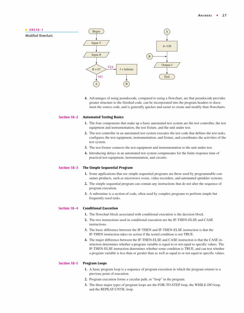
3. See Figure ANS18–1.
16 Æ
-15 V+9 V
FLOY9868_09_SE_Answer.qxd 1/11/11 12:14 AM Page 26
ANSWERS ◆ 27
4. Advantages of using pseudocode, compared to using a flowchart, are that pseudocode providesgreater structure to the finished code, can be incorporated into the program headers to docu-ment the source code, and is generally quicker and easier to create and modify than flowcharts.
Section 18–2 Automated Testing Basics
1. The four components that make up a basic automated test system are the test controller, the testequipment and instrumentation, the test fixture, and the unit under test.
2. The test controller in an automated test system executes the test code that defines the test tasks,configures the test equipment, instrumentation, and fixture, and coordinates the activities of thetest system.
3. The test fixture connects the test equipment and instrumentation to the unit under test.
4. Introducing delays in an automated test system compensates for the finite response time ofpractical test equipment, instrumentation, and circuits.
Section 18–3 The Simple Sequential Program
1. Some applications that use simple sequential programs are those used by programmable con-sumer products, such as microwave ovens, video recorders, and automated sprinkler systems.
2. The simple sequential program can contain any instructions that do not alter the sequence ofprogram execution.
3. A subroutine is a section of code, often used by complex programs to perform simple butfrequently-used tasks.
Section 18–4 Conditional Execution
1. The flowchart block associated with conditional execution is the decision block.
2. The two instructions used in conditional execution are the IF-THEN-ELSE and CASE instructions.
3. The basic difference between the IF-THEN and IF-THEN-ELSE instruction is that the IF-THEN instruction takes no action if the tested condition is not TRUE.
4. The major difference between the IF-THEN-ELSE and CASE instruction is that the CASE in-struction determines whether a program variable is equal to or not equal to specific values. TheIF-THEN-ELSE instruction determines whether some condition is TRUE, and can test whethera program variable is less than or greater than as well as equal to or not equal to specific values.
Section 18–5 Program Loops
1. A basic program loop is a sequence of program execution in which the program returns to aprevious point of execution.
2. Program execution forms a circular path, or “loop” in the program.
3. The three major types of program loops are the FOR-TO-STEP loop, the WHILE-DO loop,and the REPEAT-UNTIL loop.
End
I = Infinite
Input V
Input R
Output I
I= V/R
Begin
A
A
B
R = 0?
NO
YES
B
� ANS18–1
Modified flowchart.
FLOY9868_09_SE_Answer.qxd 1/11/11 12:14 AM Page 27

28 ◆ ANSWERS
4. A WHILE-DO loop differs from a REPEAT-UNTIL loop in that the WHILE-DO loop checksthe loop condition before executing the loop instructions rather than after, and it remains in theloop while the loop condition is TRUE rather than FALSE.
5. A nested loop is a sequence of instructions in which part of a loop is itself a loop, creating aloop within a loop.
Section 18–6 Branching and Subroutines
1. A branching instruction is an instruction that transfers control to some specific section of code.
2. The two objectives that branching accomplishes is to avoid executing code that immediatelyfollows the branching instruction, and to access code that does not immediately follow thebranching instruction.
3. Coupling reflects the extent to which one part of a program interacts with or potentially affectsanother part of the program. Cohesion refers to how well a program or procedure keeps together all the code that is associated with a specific task.
4. Three basic guidelines for using general branches in programs are (a) programs, especiallyhigh-level programs, should avoid unconditional branching, (b) programs should avoid nestedbranches, especially unconditional branches, and (c) branches should always be a consciousdesign decision to simplify the program.
5. A subroutine call differs from a general branching instruction in that once a subroutine com-pletes, the program execution automatically resumes at the instruction that immediately followsthe instruction that called the subroutine.
RELATED PROBLEMS FOR EXAMPLES18–1 Terminal B of Port 1 connects to the terminal for TP4 through the contacts of relay K8.
Relay K8 is energized.
18–2 The diode can be reverse-biased by connecting the positive and negative terminals of the dcsupply to test point terminals 3 and 1, respectively. To do so, the test controller can energizethe coils of relays K3 and K5, connecting terminals A and B of Port 1 to test point terminals3 and 1, respectively.
18–3 Two advantages of measuring the resistor value are (1) the test will compensate for variationsin resistor value due to the initial resistor tolerance, resistor aging, and ambient temperature,and (2) the test will not require modification if the resistor value in the circuit changes.
18–4 One possible pseudocode description is
program NewCalculatePowerbegin
input current valueinput resistance valuepower value is current value squared times
resistance valueoutput power value
end NewCalculatePower18–5 One possible pseudocode description is
program CalculateMaximumValuebegin
input resistance valueinput tolerance valuedeviation value is resistance value times
tolerance valuemaximum value is resistance value plus deviation valueoutput maximum value
end CalculateMaximumValue18–6 One possible pseudocode description is
program DiodeCheckbegin
apply 5 V to circuitmeasure diode voltage
FLOY9868_09_SE_Answer.qxd 1/11/11 12:14 AM Page 28
ANSWERS ◆ 29
if (diode voltage equals 0.7 V) thenbegin if
print "Diode forward biased"end if
elsebegin else
print "Diode reverse biased"end else
end DiodeCheck
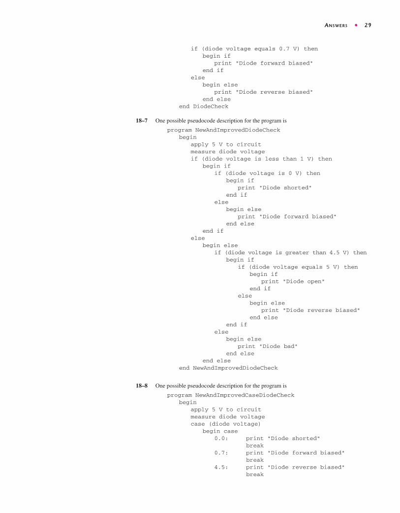
18–7 One possible pseudocode description for the program is
program NewAndImprovedDiodeCheckbegin
apply 5 V to circuitmeasure diode voltageif (diode voltage is less than 1 V) then
begin ifif (diode voltage is 0 V) then
begin ifprint "Diode shorted"
end ifelse
begin elseprint "Diode forward biased"
end elseend if
elsebegin else
if (diode voltage is greater than 4.5 V) thenbegin if
if (diode voltage equals 5 V) thenbegin if
print "Diode open"end if
elsebegin else
print "Diode reverse biased"end else
end ifelse
begin elseprint "Diode bad"
end elseend else
end NewAndImprovedDiodeCheck
18–8 One possible pseudocode description for the program is
program NewAndImprovedCaseDiodeCheckbegin
apply 5 V to circuitmeasure diode voltagecase (diode voltage)
begin case0.0: print "Diode shorted"
break0.7: print "Diode forward biased"
break4.5: print "Diode reverse biased"
break
FLOY9868_09_SE_Answer.qxd 11/30/10 6:12 PM Page 29
30 ◆ ANSWERS
5.0: print "Diode open"break
default: print "Diode bad"break
end caseend NewAndImprovedCaseDiodeCheck
If the measured diode voltage is 2.5 V, the program prints “Diode bad”.
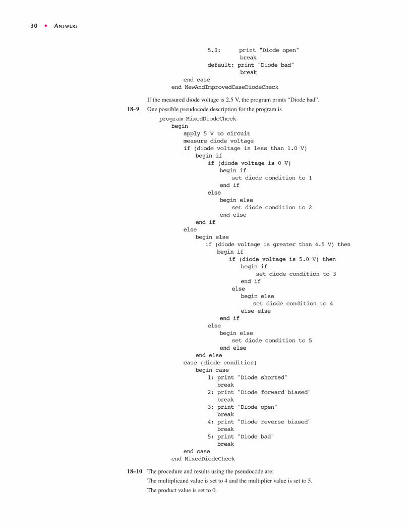
18–9 One possible pseudocode description for the program is
program MixedDiodeCheckbegin
apply 5 V to circuitmeasure diode voltageif (diode voltage is less than 1.0 V)
begin ifif (diode voltage is 0 V)
begin ifset diode condition to 1
end ifelse
begin elseset diode condition to 2
end elseend if
elsebegin else
if (diode voltage is greater than 4.5 V) thenbegin if
if (diode voltage is 5.0 V) thenbegin if
set diode condition to 3end if
elsebegin else
set diode condition to 4else else
end ifelse
begin elseset diode condition to 5
end elseend else
case (diode condition)begin case
1: print "Diode shorted"break
2: print "Diode forward biased"break
3: print "Diode open"break
4: print "Diode reverse biased"break
5: print "Diode bad"break
end caseend MixedDiodeCheck
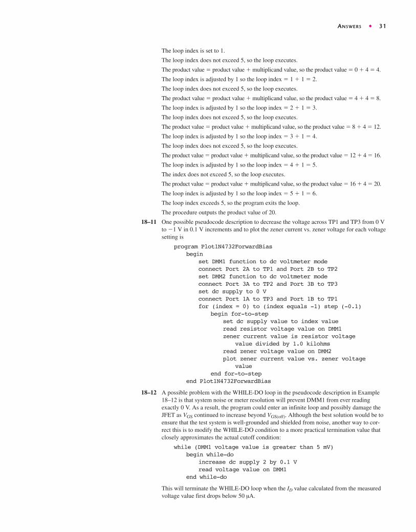
18–10 The procedure and results using the pseudocode are:
The multiplicand value is set to 4 and the multiplier value is set to 5.
The product value is set to 0.
FLOY9868_09_SE_Answer.qxd 1/11/11 12:14 AM Page 30
ANSWERS ◆ 31
The loop index is set to 1.
The loop index does not exceed 5, so the loop executes.
The product value � product value � multiplicand value, so the product value � 0 � 4 � 4.
The loop index is adjusted by 1 so the loop index � 1 � 1 � 2.
The loop index does not exceed 5, so the loop executes.
The product value � product value � multiplicand value, so the product value � 4 � 4 � 8.
The loop index is adjusted by 1 so the loop index � 2 � 1 � 3.
The loop index does not exceed 5, so the loop executes.
The product value � product value � multiplicand value, so the product value � 8 � 4 � 12.
The loop index is adjusted by 1 so the loop index � 3 � 1 � 4.
The loop index does not exceed 5, so the loop executes.
The product value � product value � multiplicand value, so the product value � 12 � 4 � 16.
The loop index is adjusted by 1 so the loop index � 4 � 1 � 5.
The index does not exceed 5, so the loop executes.
The product value � product value � multiplicand value, so the product value � 16 � 4 � 20.
The loop index is adjusted by 1 so the loop index � 5 � 1 � 6.
The loop index exceeds 5, so the program exits the loop.
The procedure outputs the product value of 20.
18–11 One possible pseudocode description to decrease the voltage across TP1 and TP3 from 0 Vto �1 V in 0.1 V increments and to plot the zener current vs. zener voltage for each voltagesetting is
program Plot1N4732ForwardBiasbegin
set DMM1 function to dc voltmeter modeconnect Port 2A to TP1 and Port 2B to TP2set DMM2 function to dc voltmeter modeconnect Port 3A to TP2 and Port 3B to TP3set dc supply to 0 Vconnect Port 1A to TP3 and Port 1B to TP1for (index = 0) to (index equals -1) step (-0.1)
begin for-to-stepset dc supply value to index valueread resistor voltage value on DMM1zener current value is resistor voltage
value divided by 1.0 kilohmsread zener voltage value on DMM2plot zener current value vs. zener voltage
valueend for-to-step
end Plot1N4732ForwardBias
18–12 A possible problem with the WHILE-DO loop in the pseudocode description in Example18–12 is that system noise or meter resolution will prevent DMM1 from ever readingexactly 0 V. As a result, the program could enter an infinite loop and possibly damage theJFET as VGS continued to increase beyond VGS(off). Although the best solution would be toensure that the test system is well-grounded and shielded from noise, another way to cor-rect this is to modify the WHILE-DO condition to a more practical termination value thatclosely approximates the actual cutoff condition:
while (DMM1 voltage value is greater than 5 mV)begin while-do
increase dc supply 2 by 0.1 Vread voltage value on DMM1
end while-do
This will terminate the WHILE-DO loop when the ID value calculated from the measuredvoltage value first drops below 50 µA.
FLOY9868_09_SE_Answer.qxd 1/11/11 12:14 AM Page 31
32 ◆ ANSWERS
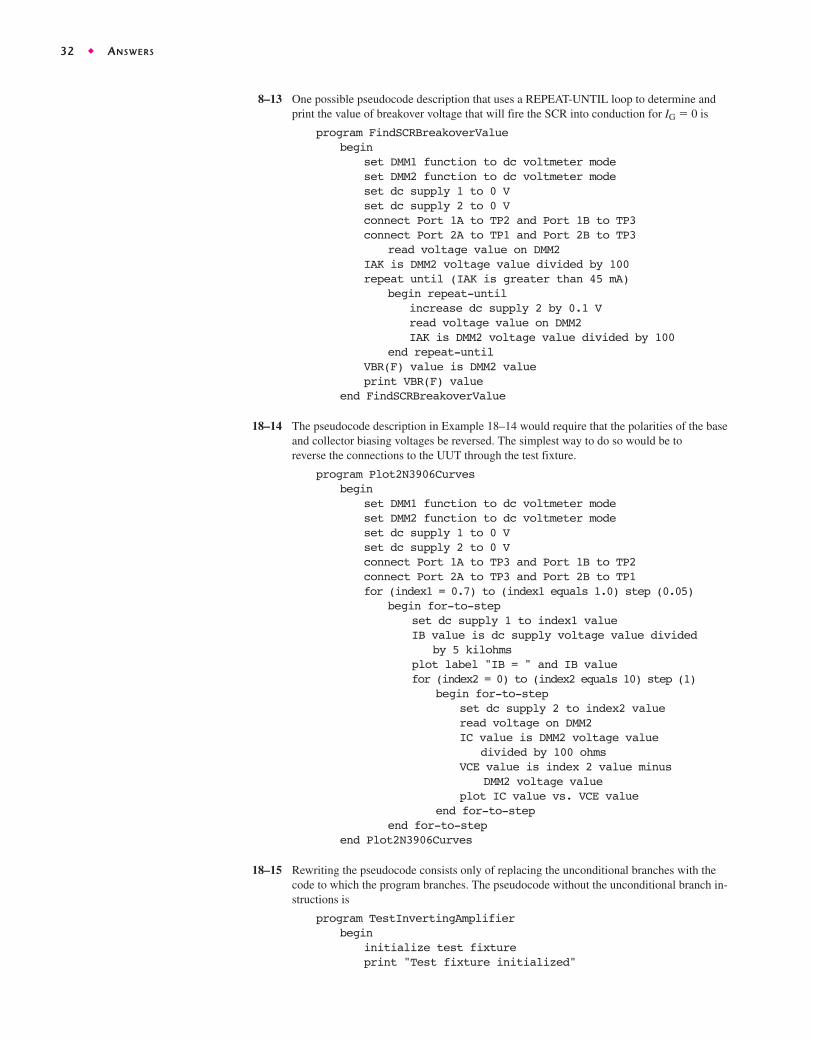
8–13 One possible pseudocode description that uses a REPEAT-UNTIL loop to determine andprint the value of breakover voltage that will fire the SCR into conduction for IG � 0 is
program FindSCRBreakoverValuebegin
set DMM1 function to dc voltmeter modeset DMM2 function to dc voltmeter modeset dc supply 1 to 0 Vset dc supply 2 to 0 Vconnect Port 1A to TP2 and Port 1B to TP3connect Port 2A to TP1 and Port 2B to TP3
read voltage value on DMM2IAK is DMM2 voltage value divided by 100repeat until (IAK is greater than 45 mA)
begin repeat-untilincrease dc supply 2 by 0.1 Vread voltage value on DMM2IAK is DMM2 voltage value divided by 100
end repeat-untilVBR(F) value is DMM2 valueprint VBR(F) value
end FindSCRBreakoverValue
18–14 The pseudocode description in Example 18–14 would require that the polarities of the baseand collector biasing voltages be reversed. The simplest way to do so would be to reverse the connections to the UUT through the test fixture.
program Plot2N3906Curvesbegin
set DMM1 function to dc voltmeter modeset DMM2 function to dc voltmeter modeset dc supply 1 to 0 Vset dc supply 2 to 0 Vconnect Port 1A to TP3 and Port 1B to TP2connect Port 2A to TP3 and Port 2B to TP1for (index1 = 0.7) to (index1 equals 1.0) step (0.05)
begin for-to-stepset dc supply 1 to index1 valueIB value is dc supply voltage value divided
by 5 kilohmsplot label "IB = " and IB valuefor (index2 = 0) to (index2 equals 10) step (1)
begin for-to-stepset dc supply 2 to index2 valueread voltage on DMM2IC value is DMM2 voltage value
divided by 100 ohmsVCE value is index 2 value minus
DMM2 voltage valueplot IC value vs. VCE value
end for-to-stepend for-to-step
end Plot2N3906Curves
18–15 Rewriting the pseudocode consists only of replacing the unconditional branches with thecode to which the program branches. The pseudocode without the unconditional branch in-structions is
program TestInvertingAmplifierbegin
initialize test fixtureprint "Test fixture initialized"
FLOY9868_09_SE_Answer.qxd 1/11/11 12:14 AM Page 32

ANSWERS ◆ 33
NewTestInit:set signal generator offset to 500 mVdcset signal generator ac output to 0 Vppprint "System intialized for dc test"
DCTest:measure and record dc output signalprint "500 mV dc test completed"dc gain value is output signal divided by 500 mVprint "Gain calculated for dc input"
ACTest:set signal generator offset to 0 Vdcset signal generator ac output to 100 mVppapply input test signalmeasure and record peak-to-peak output signalprint "100 mV ac test completed"
CalculateNominalGain:nominal gain value is output signal divided by 100 mVprint "Gain calculated for nominal input"
TestMinimumSignal:set signal generator ac output to 10 mVppmeasure and record peak-to-peak output signalprint "10 mV ac test completed"minimum gain value is output test divided by 10 mVprint "Gain calculated for minimum input"
TestMaximumSignal:set signal generator ac output to 1 Vppmeasure and record peak-to-peak output signalprint "1 V ac test completed"maximum gain value is output signalprint "Gain calculated for maximum input"
AllTestsRun:print "AC test completed"print "Inverting amplifier testing complete"
end TestInvertingAmplifier
18–16 Although the multiple instances of “measure summing amplifier output” could be re-placed with calls to a subroutine MeasureSummingAmplfiierOutput, modifying the pro-gram to do so would not provide any benefit. The overhead to call, execute, and returnfrom the procedure would take more time and require more instructions than the originalprogram requires.
18–17 One possible pseudocode description to replace the subroutines MeasureNominalGain,MeasureMinimumGain, and MeasureMaximumGain with a single subroutineMeasureGain is
program CalculateAmplifierGainsbegin
call ConfigureTestFixture (5.0)print "Test fixture initialized"NewTestInit:set signal generator offset to 500 mVdcset signal generator ac output to 0 Vppprint "System intialized for dc test"
NominalACTest:call MeasureGain(0.05)
MinimumACTest:call MeasureGain(0.5)
MaximumACTest:call MeasureGain(5.0)
AllGainsMeasured:print "AC test completed"print "Inverting amplifier testing complete"
FLOY9868_09_SE_Answer.qxd 1/11/11 12:14 AM Page 33
34 ◆ ANSWERS
call ConfigureTestFixture (0.0)end CalculateAmplifierGains
procedure ConfigureTestFixture(DCSupply1Value)begin
open all relaysset dc supply 1 to DCSupply1Valueset dc supply 2 to 0.0set dc supply 3 to 0.0
end ConfigureTestFixture
procedure MeasureGain(InputValue)begin
set signal generator offset to 0 Vdcset signal generator ac output to InputValueapply input test signalmeasure and record peak-to-peak output signalnominal gain value is output signal divided by
InputValueprint InputValue and "ac test completed"
end MeasureGain
TRUE/FALSE QUIZ1. T 2. T 3. T 4. F 5. F 6. F 7. T
8. F 9. T 10. F 11. T 12. T 13. F
SELF-TEST1. (d) 2. (b) 3. (c) 4. (c) 5. (a) 6. (d) 7. (d) 8. (c) 9. (a)
10. (b) 11. (c) 12. (a) 13. (b) 14. (c) 15. (a) 16. (d) 17. (b) 18. (a)
ANSWERS GreenTech Application
GA11. Solar module (panel) or array, Charge controller, batteries, inverter.
2. Cells must be in series to increase output voltage.
3. The charge controller maintains proper charging of the batteries.
4. The inverter converts the dc voltage from the solar panel or the batteries to ac voltage.
5. Result will vary depending on source. Typical range: voltage 12 V-48 V, power up to 200 W.
GA21. Deep-cycle batteries can be repeatedly discharged by as much as 89%.
2. Higher charge voltage ensures proper charging.
3. The MPPT charge controller is most efficient.
4. Result will vary depending on source. Up to 8400 W is typical.
5. Output voltage is 24 V. Ah rating is 500 Ah.
GA31. A stand-alone inverter is used in small systems where all the power is used on-site. The grid-tie
inverter connects to the electrical grid and supplies power to users on the grid or to users onthe grid and on-site.
2. Sine-wave and modified sine-wave inverters are common. A third type, square wave, is seldomused.
FLOY9868_09_SE_Answer.qxd 1/17/11 7:29 PM Page 34
ANSWERS ◆ 35
3. Results will vary with the individual.
4. Results will vary with the location.
5. Result will vary depending on source. Typical range: 1 kW to 100 kW.
GA41. The types of solar trackers are azimuth and elevation.
2. Azimuth trackers follow the sun’s path daily. Elevation trackers follow the sun’s position sea-sonally.
3. Winter solstice is on December 21 or December 22.
4. Summer solstice is on June 20 or June 21.
5. Results will vary. Dual-axis collects more energy year round but single axis is less expensive.
GA51. HAWT is horizontal axis wind turbine.
2. The amplitude varies depending on speed of rotation.
3. Wind velocity, air density, length of blades.
4. Betz limit is 59% of the wind energy that can be extracted.
5. Results will vary. It depends on regional laws, the size of the turbines, and the terrain.
GA61. VAWT is vertical axis wind turbine.
2. Darrieus, giromill, savonius, and helical
3. Advantages of a VAWT are that the generator and control electronics can be placed on theground and VAWTs can be placed closer together.
4. Results will vary.
FLOY9868_09_SE_Answer.qxd 1/17/11 7:30 PM Page 35
Related Documents