Influence of Crystalline Microstructure on Optical Response of Single ZnSe Nanowires by Ankur Saxena A thesis submitted in conformity with the requirements for the degree of Doctor of Philosophy Graduate Department of Materials Science and Engineering University of Toronto Copyright © 2012 by Ankur Saxena

Welcome message from author
This document is posted to help you gain knowledge. Please leave a comment to let me know what you think about it! Share it to your friends and learn new things together.
Transcript

Influence of Crystalline Microstructure on OpticalResponse of Single ZnSe Nanowires
by
Ankur Saxena
A thesis submitted in conformity with the requirementsfor the degree of Doctor of Philosophy
Graduate Department of Materials Science and EngineeringUniversity of Toronto
Copyright © 2012 by Ankur Saxena
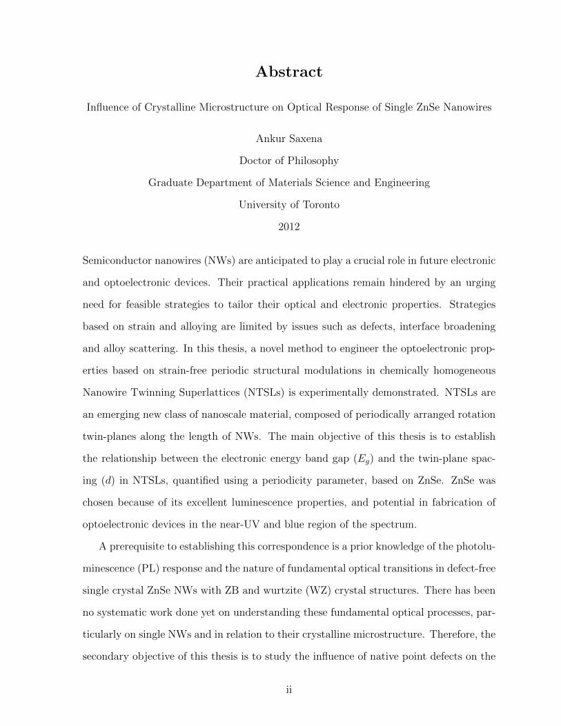
Abstract
Influence of Crystalline Microstructure on Optical Response of Single ZnSe Nanowires
Ankur Saxena
Doctor of Philosophy
Graduate Department of Materials Science and Engineering
University of Toronto
2012
Semiconductor nanowires (NWs) are anticipated to play a crucial role in future electronic
and optoelectronic devices. Their practical applications remain hindered by an urging
need for feasible strategies to tailor their optical and electronic properties. Strategies
based on strain and alloying are limited by issues such as defects, interface broadening
and alloy scattering. In this thesis, a novel method to engineer the optoelectronic prop-
erties based on strain-free periodic structural modulations in chemically homogeneous
Nanowire Twinning Superlattices (NTSLs) is experimentally demonstrated. NTSLs are
an emerging new class of nanoscale material, composed of periodically arranged rotation
twin-planes along the length of NWs. The main objective of this thesis is to establish
the relationship between the electronic energy band gap (Eg) and the twin-plane spac-
ing (d) in NTSLs, quantified using a periodicity parameter, based on ZnSe. ZnSe was
chosen because of its excellent luminescence properties, and potential in fabrication of
optoelectronic devices in the near-UV and blue region of the spectrum.
A prerequisite to establishing this correspondence is a prior knowledge of the photolu-
minescence (PL) response and the nature of fundamental optical transitions in defect-free
single crystal ZnSe NWs with ZB and wurtzite (WZ) crystal structures. There has been
no systematic work done yet on understanding these fundamental optical processes, par-
ticularly on single NWs and in relation to their crystalline microstructure. Therefore, the
secondary objective of this thesis is to study the influence of native point defects on the
ii

optical response of single ZnSe NWs in direct relation to their crystalline microstructure.
The PL response from single ZB and WZ NWs was determined unambiguously, and
excitonic emission linewidths close to 1 meV were observed, which are the narrowest
reported linewidths thus far on ZnSe NWs. Based on this and extensive optical and
structural characterization on individual NTSLs, a linear variation in Eg is shown through
a monotonic shift in PL peak position from ZnSe NTSLs as a function of d, with Eg’s
that lie between those of ZB and WZ crystal structures. This linear variation in Eg was
also validated by ab Initio electronic structure calculations. This establishes NTSLs as
new nanoscale polytypes advantageous for applications requiring tunable band gaps.
iii

Dedication
To my loving grandmother
Smt. Katori Devi
and grandfather
Sri Raj Narayan Saxena
iv

Acknowledgements
It is my distinct pleasure to thank all those who helped me in one way or another in
making this thesis possible. First and foremost, my sincerest gratitude is reserved for
my thesis supervisor, Dr. Harry E. Ruda, for his constant support, expert guidance and
consistent encouragement. I am most grateful to him for the flexibility in research he
gave me, which allowed me to perform the experimental work that I enjoyed the most.
I extend my sincere thanks to Mitsuru Sugisaki, an expert in single quantum dot
spectroscopy and a faculty member at Osaka University in Japan, who spent some
time with me in the optical lab on his brief trip to Toronto. In those few hours, I
learned immensely about the design of experimental arrangement for confocal micro-
photoluminescence spectroscopy, and ways to attain precision in optical alignment. I am
deeply indebted to my former colleague and a close friend, Usha Philipose, for providing
me with the ZnSe nanowire samples for my work. I also would like to thank Qi Pan
(Eric), a former undergraduate thesis student in my research group, for providing me
with ZnSe nanowire samples after Usha joined as a faculty member at the University of
North Texas. But for the expertise of Usha and tireless work by Eric in synthesizing
ZnSe nanowires, my research work would not have been possible.
I am grateful to Selva V. Nair, a senior scientist in my research group, who enthusi-
astically agreed to perform the electronic structure calculations on Nanowire Twinning
Superlattices. These were crucially helpful in verifying the experimental data. I am
also thankful to him for stimulating discussions at several occasions, which helped me in
my understanding of the optical processes in semiconductors. I sincerely thank Christina
Souza, and Carlos Fernandes, both senior scientists, for proof-reading my thesis and their
comments. I am very grateful to Christina for always answering my questions related to
research work, optics and instruments inside the optical lab, troubleshooting and admin-
istrative in nature. I am also thankful to Carlos for his help every time the chiller used
to break down in the optical lab.
v
The electron microscopy work described in this thesis would not have been possible
without the technical assistance from Fred Pearson and Carmen Andrei at the Canadian
Centre for Electron Microscopy (CCEM). I am thankful to both of them for doing their
best in accommodating my requests for time on the instruments, considering that these
were always booked well in advance. In particular, I am grateful to Fred for his persistence
and patience while working on my NW samples, when at times it used to take hours in
tilting the specimen holder to get the right diffraction conditions. Those familiar with
the Ti:Sapphire lasers know that they are far from being plug-and-play systems. I would
like to thank Suxia Yang who taught me how to use the Ti:Sapphire and other lasers
inside the optical lab in the first few years of my project, when I was a novice.
I would like to thank my supervisory committee members, Prof. Glenn Hibbard,
Prof. Francis Dawson and Prof. Z. H. Lu, for a careful reading of my thesis and their
invaluable inputs.
I am thankful to all graduate students in my group, former and present, in creating
a healthy work environment conducive for research. In particular, I am thankful to Joe
Salfi, my colleague for almost the entire duration of my project and a very good friend,
for his extremely useful suggestions with regards to trouble-shooting in the lab, and
frequent interesting discussions. I would also like to thank Millie Morris, our business
and administrative officer, who was always friendly and efficiently handled the matters
related to purchases and returns.
It would be an act of injustice if I do not express my gratefulness to my wife, Girija
Dharmaraj, for her immense patience, constant personal support, and encouragement at
times when experiments would not go as I had hoped. I would also like to acknowledge
her help in providing me with the MATLAB scripts at times. I am also most grateful to
my parents and my sisters, Shanu and Ankita, for their continued encouragement and
support for the duration of my research work.
I gratefully acknowledge financial support from Eleanor and Burnett Thall - Ontario
vi

Graduate Scholarship in Science and Technology (OGSST), J. Edgar McAllister Grad-
uate Award, University of Toronto Open fellowships, funding from Dr. Ruda and the
Department of Materials Science and Engineering at the University of Toronto. The
electron microscopy research described in this thesis was performed at the CCEM, which
is supported by NSERC and other government agencies.
vii

Contents
Abstract ii
List of Tables xii
List of Figures xvi
List of Acronyms xxxi
List of Symbols xxxv
Glossary of terms xliii
1 Background-Current state of the art 1
1.1 Introduction . . . . . . . . . . . . . . . . . . . . . . . . . . . . . . . . . . 1
1.1.1 II-VI compound semiconductors . . . . . . . . . . . . . . . . . . . 1
1.1.2 ZnSe for opto-electronic devices . . . . . . . . . . . . . . . . . . . 2
1.2 Semiconductor nanowires . . . . . . . . . . . . . . . . . . . . . . . . . . . 3
1.2.1 ZnSe nanowires . . . . . . . . . . . . . . . . . . . . . . . . . . . . 5
1.3 Semiconductor nanowire heterostructures . . . . . . . . . . . . . . . . . . 6
1.3.1 Nanowire Twinning Superlattices (NTSLs) . . . . . . . . . . . . . 7
1.4 Growth of semiconductor nanowires . . . . . . . . . . . . . . . . . . . . . 10
1.4.1 Growth and structural characterization of ZnSe nanowires . . . . 12
1.5 Luminescence characterization of ZnSe single crystals and thin films . . . 13
viii
1.5.1 Characteristic features of ZnSe LTPL spectrum . . . . . . . . . . 15
1.5.2 Excitonic emission in ZnSe . . . . . . . . . . . . . . . . . . . . . . 17
1.6 Optical response of ZnSe nanowires . . . . . . . . . . . . . . . . . . . . . 19
1.6.1 Distinction from ZnSe single crystals and thin films . . . . . . . . 19
Distinguishing features . . . . . . . . . . . . . . . . . . . . . . . . 20
Confinement effects in nanowires . . . . . . . . . . . . . . . . . . 21
1.6.2 Luminescence characterization of ZnSe nanowires . . . . . . . . . 22
1.6.3 Influence of heat treatment . . . . . . . . . . . . . . . . . . . . . . 25
1.7 Summary . . . . . . . . . . . . . . . . . . . . . . . . . . . . . . . . . . . 28
2 Motivation and Objectives 30
2.1 Introduction . . . . . . . . . . . . . . . . . . . . . . . . . . . . . . . . . . 30
2.2 Motivation . . . . . . . . . . . . . . . . . . . . . . . . . . . . . . . . . . . 31
2.3 Gaps in the understanding of fundamental optical transitions in ZnSe NWs
in literature . . . . . . . . . . . . . . . . . . . . . . . . . . . . . . . . . . 34
2.3.1 Role of native point defects . . . . . . . . . . . . . . . . . . . . . 35
2.3.2 Lack of luminescence studies on single ZnSe nanowires . . . . . . 37
2.4 Objectives . . . . . . . . . . . . . . . . . . . . . . . . . . . . . . . . . . . 42
3 Experimental Methodology 44
3.1 Introduction . . . . . . . . . . . . . . . . . . . . . . . . . . . . . . . . . . 44
3.2 Rationale behind the choice of experimental techniques . . . . . . . . . . 46
3.2.1 Advantages of PL spectroscopy . . . . . . . . . . . . . . . . . . . 47
3.2.2 Limitations of PL spectroscopy . . . . . . . . . . . . . . . . . . . 49
3.3 Growth of ZnSe nanowires and NTSLs . . . . . . . . . . . . . . . . . . . 50
3.4 Obstacles in combined optical and structural characterization of the same
individual nanowire . . . . . . . . . . . . . . . . . . . . . . . . . . . . . . 51
ix

3.4.1 Bottleneck - incompatible sample preparation methods for different
techniques . . . . . . . . . . . . . . . . . . . . . . . . . . . . . . . 53
3.5 Photoluminescence (PL) spectroscopy . . . . . . . . . . . . . . . . . . . . 56
3.6 Confocal Micro-photoluminescence (µ-PL) Spectroscopy . . . . . . . . . 61
3.7 Time-resolved Photoluminescence (TRPL) . . . . . . . . . . . . . . . . . 66
3.8 Transmission Electron Microscopy (TEM) . . . . . . . . . . . . . . . . . 69
3.9 Acquisition and analysis of PL results . . . . . . . . . . . . . . . . . . . . 70
3.9.1 Data acquisition . . . . . . . . . . . . . . . . . . . . . . . . . . . . 70
Integration time ti . . . . . . . . . . . . . . . . . . . . . . . . . . 71
Slit-width dslit . . . . . . . . . . . . . . . . . . . . . . . . . . . . . 72
Excitation Intensity Iexc . . . . . . . . . . . . . . . . . . . . . . . 73
3.9.2 Spectral correction and normalization of PL spectra . . . . . . . . 74
Spectral correction . . . . . . . . . . . . . . . . . . . . . . . . . . 74
Normalization of PL spectra . . . . . . . . . . . . . . . . . . . . . 75
3.9.3 Data analysis using curve-fitting . . . . . . . . . . . . . . . . . . . 77
3.10 Summary . . . . . . . . . . . . . . . . . . . . . . . . . . . . . . . . . . . 79
4 Influence of stoichiometry on optical response 82
4.1 Introduction . . . . . . . . . . . . . . . . . . . . . . . . . . . . . . . . . . 82
4.2 Results . . . . . . . . . . . . . . . . . . . . . . . . . . . . . . . . . . . . . 83
4.2.1 Low-temperature PL spectra . . . . . . . . . . . . . . . . . . . . . 83
4.2.2 Excitation intensity dependence of PL spectra . . . . . . . . . . . 85
4.3 Discussion . . . . . . . . . . . . . . . . . . . . . . . . . . . . . . . . . . . 89
4.4 Conclusions . . . . . . . . . . . . . . . . . . . . . . . . . . . . . . . . . . 97
5 Single zinc-blende ZnSe nanowires 99
5.1 Introduction . . . . . . . . . . . . . . . . . . . . . . . . . . . . . . . . . . 99
5.2 Results and Discussion . . . . . . . . . . . . . . . . . . . . . . . . . . . . 100
x
5.2.1 Characterization of single ZB ZnSe NWs . . . . . . . . . . . . . . 100
HR-TEM characterization . . . . . . . . . . . . . . . . . . . . . . 101
Low-temperature PL spectra . . . . . . . . . . . . . . . . . . . . . 101
5.2.2 Comparison with an ensemble of ZB NWs . . . . . . . . . . . . . 111
5.2.3 Dependence of PL on temperature . . . . . . . . . . . . . . . . . 115
5.2.4 Dependence of LTPL on Iexc . . . . . . . . . . . . . . . . . . . . . 126
5.3 Conclusions . . . . . . . . . . . . . . . . . . . . . . . . . . . . . . . . . . 126
6 Single wurtzite ZnSe nanowires 130
6.1 Introduction . . . . . . . . . . . . . . . . . . . . . . . . . . . . . . . . . . 130
6.2 Results and Discussion . . . . . . . . . . . . . . . . . . . . . . . . . . . . 131
6.2.1 Characterization of single WZ nanowires . . . . . . . . . . . . . . 131
HR-TEM characterization . . . . . . . . . . . . . . . . . . . . . . 132
Low-temperature PL spectra . . . . . . . . . . . . . . . . . . . . . 134
6.2.2 Dependence of PL on temperature . . . . . . . . . . . . . . . . . 141
6.2.3 Dependence of LTPL on Iexc . . . . . . . . . . . . . . . . . . . . . 145
6.3 Conclusions . . . . . . . . . . . . . . . . . . . . . . . . . . . . . . . . . . 148
7 ZnSe Nanowire Twinning Superlattices 150
7.1 Introduction . . . . . . . . . . . . . . . . . . . . . . . . . . . . . . . . . . 150
7.1.1 Periodicity parameter (γ) . . . . . . . . . . . . . . . . . . . . . . 151
7.1.2 Excitation intensity dependence of LTPL . . . . . . . . . . . . . . 157
7.2 Variation in band gap of NTSLs . . . . . . . . . . . . . . . . . . . . . . . 159
7.3 Time-resolved photoluminescence . . . . . . . . . . . . . . . . . . . . . . 162
7.4 Dependence of PL on temperature . . . . . . . . . . . . . . . . . . . . . . 166
7.5 Conclusions . . . . . . . . . . . . . . . . . . . . . . . . . . . . . . . . . . 170
8 Conclusions and Outlook 173
8.1 Outlook . . . . . . . . . . . . . . . . . . . . . . . . . . . . . . . . . . . . 182
xi
A Bound-exciton lines in ZnSe films 184
B Survey of luminescence studies on ZnSe nanostructures 187
C Photoluminescence (PL) Spectroscopy 194
C.1 Principles . . . . . . . . . . . . . . . . . . . . . . . . . . . . . . . . . . . 194
C.2 Theoretical models . . . . . . . . . . . . . . . . . . . . . . . . . . . . . . 202
C.2.1 Excitation intensity dependence of PL . . . . . . . . . . . . . . . 202
Dependence of IPL on Iexc . . . . . . . . . . . . . . . . . . . . . . 203
Dependence of peak energy on Iexc . . . . . . . . . . . . . . . . . 204
C.2.2 Temperature dependence of PL . . . . . . . . . . . . . . . . . . . 205
Dependence of peak energy on T . . . . . . . . . . . . . . . . . . 205
Dependence of HWHM on T . . . . . . . . . . . . . . . . . . . . . 207
Dependence of IPL on T . . . . . . . . . . . . . . . . . . . . . . . 208
D Time-resolved Photoluminescence (TRPL) spectroscopy 211
E Electronic band structures 214
E.1 Energy band diagrams . . . . . . . . . . . . . . . . . . . . . . . . . . . . 214
E.2 Band structure calculations for Nanowire Twinning Superlattices . . . . . 217
F Softwares and Programs used 221
G Supplementary TEM micrographs 223
G.1 Chapter 5 - ZB ZnSe nanowires . . . . . . . . . . . . . . . . . . . . . . . 223
G.2 Chapter 6 - WZ ZnSe nanowires . . . . . . . . . . . . . . . . . . . . . . . 225
G.3 Chapter 7 - ZnSe NTSLs . . . . . . . . . . . . . . . . . . . . . . . . . . . 225
Bibliography 240
Author Index 279
xii

List of Tables
4.1 Table showing the values of different fitting parameters of Equation 4.3 . 93
5.1 Experimental and calculated ratios of the intensity of the m-th order LO-
phonon replica (Im) to that of the ZPL (I(m=0)) for the Id1 and Id′
1 lines.
The calculated ratios were found using Equation 5.2. Nph are the values
in columns (2) and (4) corresponding to m = 1. The intensity ratios are
listed for ZB-NW-1, 2 and 3, and a bundle of ZB NWs. These ratios
reported by Jiang et al. are also listed [287]. . . . . . . . . . . . . . . . . 109
5.2 Values of the fit parameters of the Varshni’s equation (Equation 5.3) which
describes the temperature dependence of the Eg. (See Figure 5.10). The
values reported previously by other authors are also listed for comparison.
A fitting error of 0 indicates error of the order of 10−5 eV. . . . . . . . . 117
5.3 Values of the fit parameters of the Bose-Einstein type expression (Equa-
tion 5.4) which describes the temperature dependence of the direct Eg.
(See Figures 5.10 and 5.11 (a,b)). The values reported by Malikova et
al. [263] are also listed for comparison. A fitting error of 0 indicates error
of the order of 10−5 eV. . . . . . . . . . . . . . . . . . . . . . . . . . . . . 120
5.4 Values of the fit parameters of the Equation 5.5 which describes the tem-
perature dependence of the exciton linewidth (HWHM). (See Figures 5.12
and 5.13 (a,b)). The values previously reported by other authors are also
listed for comparison. . . . . . . . . . . . . . . . . . . . . . . . . . . . . . 122
xiii

6.1 Phonon energies of the acoustic and optical phonons in WZ ZnSe, as given
by Liang and Yoffe [305]. . . . . . . . . . . . . . . . . . . . . . . . . . . . 135
6.2 Proposed assignments of the PL peaks observed in the LTPL spectrum
from WZ-NW-1. The assignment given by Liang and Yoffe [305] are also
given as a reference for the common peaks observed, and I1 and I2 peaks
(their notation). . . . . . . . . . . . . . . . . . . . . . . . . . . . . . . . . 138
6.3 Experimental and calculated ratios of the intensity of the m-th order LO-
phonon replica (Im) to that of the ZPL (I(m=0)) for the DAP-related tran-
sitions in the LTPL from WZ-NW-1. The calculated ratios were found
using Equation 5.2. Nph are the values in columns (3) and (6) correspond-
ing to m = 1. The values of these ratios given by Liang and Yoffe [305]
are also given for comparison. . . . . . . . . . . . . . . . . . . . . . . . . 139
6.4 Values of the fit parameters of the Bose-Einstein type expression (Equa-
tion 5.4) which describes the temperature dependence of the direct Eg.
(See Figure 6.8). . . . . . . . . . . . . . . . . . . . . . . . . . . . . . . . 143
6.5 Values of the fit parameters of the Equation 5.5 which describes the tem-
perature dependence of the exciton linewidth (HWHM). (See Figure 6.10).
The values obtained for the Id1 line for ZB-NW-3 are also listed for com-
parison. . . . . . . . . . . . . . . . . . . . . . . . . . . . . . . . . . . . . 148
7.1 Twin-plane spacing d, error in d (δd) (s.e.m.) and dispersion in twin-plane
spacing ∆d (s.d.) for NTSLs 1-5 whose distributions of segment widths
are shown in Figure 7.2. NS is the sample size. Also listed are the results
of Kolmogorov Smirnov (K-S) normality test (for an alpha level of 0.05)
for the distributions. . . . . . . . . . . . . . . . . . . . . . . . . . . . . . 155
7.2 Values of the fit parameters of Equations 5.3 (Varshni’s equation) and 5.4
(Bose-Einstein type expression) which describe the temperature depen-
dence of the Eg. . . . . . . . . . . . . . . . . . . . . . . . . . . . . . . . . 168
xiv

7.3 Values of the fit parameters of Equation 5.5 which describes the temper-
ature dependence of the exciton linewidth (HWHM). . . . . . . . . . . . 170
8.1 Summary of the recombination lines identified in ZB and WZ ZnSe NWs.
The exciton binding energies (EBX) for donor and acceptor bound exci-
tons, ionization energies of the donors (ED) and acceptors (EA) are also
listed. . . . . . . . . . . . . . . . . . . . . . . . . . . . . . . . . . . . . . 180
8.2 Summary of the values of the fit parameters determined using dependene
of PL on temperature for single ZB and WZ NWs and a single NTSL. . . 181
A.1 Donors and donor-bound excitons in ZnSe films. Line positions at 4.2
K. EBX(D0X) exciton-donor binding energy, ED donor ionization energy,
dfilm film thickness. Reprinted with permission from Ref. [7] © 1990 John
Wiley & Sons. . . . . . . . . . . . . . . . . . . . . . . . . . . . . . . . . . 185
A.2 Acceptors and acceptor-exciton complexes in ZnSe films. Line positions at
4.2 K. EBX(A0X) exciton-acceptor binding energy, EA acceptor ionization
energy, dfilm film thickness. Reprinted with permission from Ref. [7] ©
1990 John Wiley & Sons. . . . . . . . . . . . . . . . . . . . . . . . . . . . 186
B.1 Summary of room-temperature and low-temperature luminescence (PL
and CL) studies on ZnSe nanostructures. Also included are reported crys-
tal structures and morphologies of nanostructures. . . . . . . . . . . . . . 187
B.2 Summary of energy positions of the near band-edge (NBE) peak and deep-
level (DL) emission band reported for ZnSe nanostructures using their
RTPL characterization. . . . . . . . . . . . . . . . . . . . . . . . . . . . 188
B.3 Summary of LTPL studies on ZnSe nanowires. The energy position(s) of
the PL line(s), their assignment(s)a, ionization energies of the donors (ED)
and acceptors (EA), temperature of the experiments, and any intentional
doping carried out are listed. . . . . . . . . . . . . . . . . . . . . . . . . . 189
xv

List of Figures
1.1 (a) A schematic illustration of a photodetector device based on an indi-
vidual single crystal ZnSe nanobelt whose SEM image is shown in (b). (c)
SEM image of a photodetector based on a single ZnSe NW. The image
shows a four-terminal contact structure. The scale bar is 4 µm. Reprinted
with permission from (a,b) Ref. [121] © 2009 John Wiley & Sons, and (c)
Ref. [71] © 2006 American Institute of Physics. . . . . . . . . . . . . . . 5
1.2 (a,b) Overview and (c) high-resolution TEM images of InP NWs of differ-
ent diameters. Scale bars in (a) 100 nm, (b) 50 nm and (c) 5 nm. There is
no fixed viewing direction because of the different orientations of NWs. (d)
TEM image of an InAs NW viewed along the 〈110〉 direction showing the
periodically arranged twin-planes. (e) An atomic model of a section of a
NTSL with the locations of twin-planes marked by arrows. The twin-plane
spacing (d) is the spacing between two consecutive twin-planes, e.g. the
distance between the planes marked by A and C. Reprinted with permis-
sion from (a,b,c) Ref. [132], (d) Ref. [124] © 2008 Macmillan Publishers
Ltd., and (e) Ref. [122] © 2011 IEEE. . . . . . . . . . . . . . . . . . . . 8
1.3 Schematic illustrating the principles of growth of NWs based on a Vapour-
Liquid-Solid (VLS) growth mechanism. See text for details. . . . . . . . . 11
xvi
1.4 Near band-edge luminescence at 1.6 K from Ga-doped ZnSe layer grown
epitaxially on GaAs (100) substrate. General features of the spectrum are
explained in the text. Reprinted with permission from Ref. [7] © 1990
John Wiley & Sons. . . . . . . . . . . . . . . . . . . . . . . . . . . . . . . 16
1.5 (a) RTCL spectrum from an individual ZnSe NW showing two peaks re-
lated to NBE and DL emission at 2.68 eV and 1.96 eV, respectively. (b)
LTPL spectrum (10 K) from an array of Ag-doped ZnSe NWs. Inset shows
the near band-edge region enlarged. See text for details. Reprinted with
permission from (a) Ref. [102] © 2011 Elsevier, and (b) Ref. [106] © 2011
American Institute of Physics. . . . . . . . . . . . . . . . . . . . . . . . . 24
1.6 RTPL spectrum from ZnSe NWs: (a) grown under Zn-rich conditions
showing stronger NBE emission compared to the weaker DL emission,
and (b) grown under Se-rich conditions showing strong DL emission while
NBE emission is absent. Insets show dominating (a) blue and (b) red
luminescence from single ZnSe NWs. Reprinted with permission from
Ref. [72] © 2006 American Institute of Physics. . . . . . . . . . . . . . . 26
3.1 A schematic of the experimental arrangement used for PL spectroscopy.
(M=mirrors, FM=flip-mirrors (mirrors on flip mounts), BS=beam-splitters,
LS=laser spectrometer, AC=auto-correlator) . . . . . . . . . . . . . . . . 58
3.2 Photograph of a section of the experimental arrangement for PL spec-
troscopy. The optical fibre is placed close to the microscope objective. . . 59
3.3 Photograph of the experimental arrangement for confocal µ-PL spectroscopy.
Inset in the lower right corner shows the confocal part with a pin-hole in
the focal plane. . . . . . . . . . . . . . . . . . . . . . . . . . . . . . . . . 62
3.4 Schematic of the confocal µ-PL spectroscopy setup. Inset: Area on an
as-grown sample excited by the laser. The laser spot is elliptical due to
the oblique incidence of the exciting laser beam. . . . . . . . . . . . . . . 64
xvii

3.5 A simplified schematic of the detection of time-resolved photoluminescence
TRPL using a streak camera. . . . . . . . . . . . . . . . . . . . . . . . . 67
4.1 (a) LTPL spectrum from ZnSe NWs grown under excess Zn growth condi-
tions. The PL was taken at 3.1 K with average Iexc=5 W/cm2. (b) Near
band-edge region of the spectrum shown in (a), showing three peaks and
a shoulder near the lowest energy peak. These peaks can be resolved into
five different emission peaks. . . . . . . . . . . . . . . . . . . . . . . . . . 83
4.2 (a) LTPL spectrum from ZnSe NWs grown under excess Se growth condi-
tions. The PL was taken at 3.1 K with average Iexc=2.5 W/cm2. (b) Near
band-edge region of the spectrum shown in (a), showing a broad peak.
This peak can be resolved to show two different emission peaks. . . . . . 84
4.3 Dependence of PL from ZnSe NWs grown with excess Zn on Iexc. The
average Iexc was varied from 50 mW/cm2 to 25 W/cm2. All spectra were
recorded at 3.1 K. . . . . . . . . . . . . . . . . . . . . . . . . . . . . . . . 86
4.4 Change of integrated PL intensity (IPL) for individual emission peaks
shown in Figure 4.1 (b) with Iexc (log-log scale). The plots have been
offset for clarity. The solid line is a fit to Equation (4.1). See text for
more details. . . . . . . . . . . . . . . . . . . . . . . . . . . . . . . . . . . 88
4.5 Variation of peak energy with Iexc for emission peak B at 2.714 eV (shown
in Figure 4.1 (b)). The solid line is a fit to the Equation 4.3. . . . . . . . 90
4.6 Variation of peak energy with Iexc for emission peak C at 2.686 eV (shown
in Figure 4.1 (b)). The solid line is a fit to the Equation 4.3. . . . . . . . 91
5.1 Structural characterization of ZB-NW-1: (a) Overview TEM micrograph,
(b) HR-TEM micrograph from an area of ZB-NW-1, and (c) Indexed SAD
pattern. The indexed spots correspond to a ZB crystal structure. The
viewing direction for (b) and (c) is 〈110〉. . . . . . . . . . . . . . . . . . . 102
xviii

5.2 (a) HR-TEM micrograph from an area of ZB-NW-1, (b) Indexed FFT
pattern taken from the area squared (in red) in (a). The indexed spots
correspond to a ZB crystal structure. The viewing direction corresponds
to 〈110〉. . . . . . . . . . . . . . . . . . . . . . . . . . . . . . . . . . . . . 103
5.3 Excitonic region of the LTPL spectrum (3.5 K) from ZB-NW-1 acquired
under the conditions of high-throughput. (Iexc and dslit are as indicated).
The inset shows a confocal PL image of ZB-NW-1 under laser excitation
with an average Iexc=12.7 W/cm2. The diameter of pin-hole in the PL
image is 5 µm. The LTPL spectrum was fit to individual emission peaks
using Lorentzians as shown. . . . . . . . . . . . . . . . . . . . . . . . . . 104
5.4 Excitonic region of the LTPL spectrum (3.6 K) acquired from ZB-NW-2
under the conditions of (a) high-throughput, and (b) high-resolution. (Iexc
and dslit are as indicated). The inset in (a) shows a confocal PL image
of ZB-NW-2 under laser excitation with average Iexc=12.7 W/cm2. The
LTPL spectra were fit to individual emission peaks using Lorentzians as
shown. . . . . . . . . . . . . . . . . . . . . . . . . . . . . . . . . . . . . . 106
5.5 Excitonic region of the LTPL spectrum (3.8 K) acquired from ZB-NW-
3 under the conditions of (a) high-throughput, and (b) high-resolution.
(Iexc and dslit are as indicated). The LTPL spectra were fit to individual
emission peaks using Lorentzians as shown. . . . . . . . . . . . . . . . . . 107
5.6 Excitonic region of the LTPL spectrum (3.7 K) from ZB-NW-1 acquired
under the conditions of high-resolution. (Iexc and dslit are as indicated).
The inset shows a confocal PL image of ZB-NW-1 under laser excitation
with an average Iexc=12.7 W/cm2. The diameter of pin-hole in the PL
image is 5 µm. The LTPL spectrum was fit to individual emission peaks
using Lorentzians as shown. . . . . . . . . . . . . . . . . . . . . . . . . . 110
xix

5.7 Excitonic region of the LTPL spectrum (3.9 K) from a bundle of ZB
NWs acquired under the conditions of (a) high-throughput, and (b) high-
resolution. (Iexc and dslit are as indicated). The inset in (a) shows a
confocal PL image of the bundle of ZB NWs under laser excitation with
average Iexc=12.7 W/cm2. The LTPL spectra were fit to individual emis-
sion peaks using Lorentzians as shown. . . . . . . . . . . . . . . . . . . . 112
5.8 Excitonic region of the LTPL spectrum (4.0 K) acquired from ZB-NW-4
with (a) dslit=50 µm and (b) dslit=100 µm. The LTPL spectra were fit to
individual emission peaks (only the Id1 line is shown in each case). The Γp
of the Id1 lines are (a) 1.5 meV and (b) 1.6 meV. . . . . . . . . . . . . . . 114
5.9 Temperature dependent PL spectra from ZB-NW-3. All spectra were ac-
quired at a fixed average Iexc=31.8 W/cm2, are normalized by the integra-
tion times (ti) and displayed offset for clarity. The LTPL spectra taken at
temperatures above 115 K are not shown. . . . . . . . . . . . . . . . . . 116
5.10 Variation in PL peak energy of the FX emission (Ep=2.800 eV) (for ZB-
NW-3) with temperature. The solid and dashed lines are fits to the Equa-
tion 5.3 and 5.4, respectively. . . . . . . . . . . . . . . . . . . . . . . . . 118
5.11 Variation in PL peak energies for the (a) Id1 and (b) Id′
1 lines (for ZB-NW-3)
with temperature. The solid line are fits to the Equation 5.4. . . . . . . . 119
5.12 Change in HWHM for the FX emission (Ep=2.800 eV) with temperature
(for ZB-NW-3). The solid line is a fit to the Equation 5.5. . . . . . . . . 121
5.13 Change in HWHM for the (a) Id1 and (b) Id′
1 lines with temperature (for
ZB-NW-3). The solid lines are fits to the Equation 5.5. . . . . . . . . . . 123
5.14 Change in integrated PL intensity (IPL) for the FX emission (Ep=2.800
eV) with temperature (for ZB-NW-3). The dashed and solid lines are fits
to the Equations 5.6 and 5.7, respectively. Note the log scale for IPL. . . 124
xx

5.15 Change in integrated PL intensity (IPL) for the (a) Id1 and (b) Id′
1 lines with
temperature (for ZB-NW-3). The solid lines are fits to the Equation 5.6.
Note the log scale for IPL. . . . . . . . . . . . . . . . . . . . . . . . . . . 125
5.16 Iexc-dependent LTPL spectra from ZB-NW-1. All spectra were acquired
at a constant temperature (3.9 K), are normalized to unity and displayed
offset for clarity. . . . . . . . . . . . . . . . . . . . . . . . . . . . . . . . . 127
6.1 Structural characterization of WZ-NW-1: (a) Overview TEM micrograph,
and (b) TEM micrograph at a magnification higher than in (a). The circle
denotes the area from where the SAD pattern (shown in Figure 6.3 (b))
was taken. . . . . . . . . . . . . . . . . . . . . . . . . . . . . . . . . . . . 132
6.2 (a) HR-TEM micrograph from an area of WZ-NW-1, (b) Indexed FFT
pattern taken from the area squared (in red) in (a). The indexed spots
correspond to a WZ crystal structure. The viewing direction for (a) and
(b) is 〈1100〉. . . . . . . . . . . . . . . . . . . . . . . . . . . . . . . . . . 133
6.3 (a) HR-TEM micrograph from another area, and (b) SAD pattern acquired
from a larger area (shown in Figure 6.1(b)) of WZ-NW-1 . The indexed
spots correspond to a WZ crystal structure. The viewing direction for (a)
and (b) is 〈1100〉. . . . . . . . . . . . . . . . . . . . . . . . . . . . . . . . 133
6.4 Excitonic region of the LTPL spectrum (3.8 K) from WZ-NW-1 acquired
under the conditions of high-throughput. (Iexc and dslit are as indicated).
The inset shows a confocal PL image of WZ-NW-1 under laser excita-
tion with an average Iexc=12.7 W/cm2. The LTPL spectrum was fit to
individual emission peaks using Lorentzians as shown. . . . . . . . . . . . 136
xxi
6.5 (a,b) Excitonic region of the LTPL spectrum (3.8 K) from WZ-NW-1
acquired under the conditions of high-resolution. (Iexc and dslit are as
indicated). The I1 line with a Γp=2.8 meV is shown in (a). The LTPL
spectrum was fit to individual emission peaks using Lorentzians as shown
in (b). . . . . . . . . . . . . . . . . . . . . . . . . . . . . . . . . . . . . . 140
6.6 Excitonic region of the LTPL spectrum (4.0 K) acquired from WZ-NW-2
under the conditions of (a) high-throughput, and (b) high-resolution. (Iexc
and dslit are as indicated). The inset in (a) shows a confocal PL image
of WZ-NW-2 under laser excitation with average Iexc=12.7 W/cm2. The
LTPL spectra in both cases were fit to individual emission peaks using
Lorentzians as shown. . . . . . . . . . . . . . . . . . . . . . . . . . . . . . 141
6.7 Temperature dependent PL spectra from WZ-NW-1. All spectra were
acquired at a fixed average Iexc=38.2 W/cm2, are normalized by the inte-
gration times (ti) and displayed offset for clarity. The LTPL spectra taken
at temperatures above 70 K are not shown. . . . . . . . . . . . . . . . . . 142
6.8 Variation in PL peak energy of the I1 line (Ep=2.841 eV) (for WZ-NW-1)
with temperature. The solid and dashed lines are fits to the Equation 5.4
for temperatures above 30 K and 40 K, respectively. . . . . . . . . . . . . 144
6.9 Change in integrated PL intensity (IPL) for the I1 line with temperature
(for WZ-NW-1). The solid line is a fit to the Equation 5.6. Note the log
scale for IPL. . . . . . . . . . . . . . . . . . . . . . . . . . . . . . . . . . 145
6.10 Change in HWHM for the I1 line (Ep=2.841 eV) with temperature (for
WZ-NW-1). The solid line is a fit to the Equation 5.5. . . . . . . . . . . 146
6.11 Iexc-dependent LTPL spectra from WZ-NW-1. All spectra were acquired
at a constant temperature (3.8 K), are normalized to unity and displayed
offset for clarity. . . . . . . . . . . . . . . . . . . . . . . . . . . . . . . . . 147
xxii

7.1 Structural characterization of representative ZnSe NTSLs: HR-
TEM micrographs of ZnSe (a) NTSL-1(γ=0.100), (b) NTSL-2(γ=0.077)
and (c) NTSL-3(γ=0.059) viewed along the 〈110〉 zone-axis of NTSLs
showing the periodically arranged twin-planes. (d) Normal percentile dis-
tribution of segment widths (nm) of ZnSe NSTL-3(0.059) with d=5.63±0.07
nm (s.e.m.) and ∆d=0.65 nm (s.d.). A narrow distribution indicates a
high degree of periodicity of twin-plane spacings in NTSL-3(0.059). Nor-
mality tests are described in Table 7.1. (e) Indexed spots in the power
spectrum taken from the area highlighted in (c) confirm that the indi-
vidual domains are 〈111〉-ZB ZnSe with 〈111〉-direction coinciding with
the growth direction of NTSL-3(0.059). (f) Indexed SAD pattern from an
area of ZnSe NTSL-3(0.059), double diffraction spots in the SAD pattern
further demonstrate the excellent periodicity of twin-plane spacing d. . . 153
7.2 Histograms representing the distributions of segment widths (nm) for NTSLs
1-5. The dashed curves are normal approximations to the distributions.
The corresponding twin-plane spacing d, error in d (δd) (s.e.m.) and dis-
persion in twin-plane spacing ∆d (s.d.) are listed in Table 7.1 along with
the results of the normality tests. . . . . . . . . . . . . . . . . . . . . . . 154
xxiii
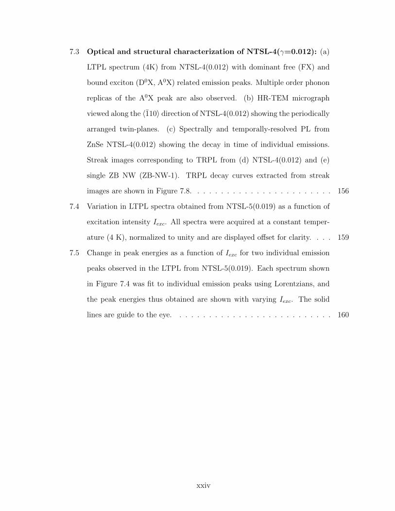
7.3 Optical and structural characterization of NTSL-4(γ=0.012): (a)
LTPL spectrum (4K) from NTSL-4(0.012) with dominant free (FX) and
bound exciton (D0X, A0X) related emission peaks. Multiple order phonon
replicas of the A0X peak are also observed. (b) HR-TEM micrograph
viewed along the 〈110〉 direction of NTSL-4(0.012) showing the periodically
arranged twin-planes. (c) Spectrally and temporally-resolved PL from
ZnSe NTSL-4(0.012) showing the decay in time of individual emissions.
Streak images corresponding to TRPL from (d) NTSL-4(0.012) and (e)
single ZB NW (ZB-NW-1). TRPL decay curves extracted from streak
images are shown in Figure 7.8. . . . . . . . . . . . . . . . . . . . . . . . 156
7.4 Variation in LTPL spectra obtained from NTSL-5(0.019) as a function of
excitation intensity Iexc. All spectra were acquired at a constant temper-
ature (4 K), normalized to unity and are displayed offset for clarity. . . . 159
7.5 Change in peak energies as a function of Iexc for two individual emission
peaks observed in the LTPL from NTSL-5(0.019). Each spectrum shown
in Figure 7.4 was fit to individual emission peaks using Lorentzians, and
the peak energies thus obtained are shown with varying Iexc. The solid
lines are guide to the eye. . . . . . . . . . . . . . . . . . . . . . . . . . . 160
xxiv

7.6 Variation in PL spectra as a function of periodicity parameter γ:
(a) LTPL (4K) spectra obtained from five different NTSLs with varying
periodicity parameters γ. Periodicity parameter γ and the order of the
polytype (2/γ)H (or 2NH) are indicated in the figure. Also shown are
the experimentally obtained PL spectra from single ZB (γ=0), and single
WZ(2H) (γ=1) NWs. There is a monotonic blue-shift in LTPL spectra
with increasing γ indicating the increase in energy band gap for polytypes
of ZnSe with maximum band gap for WZ ZnSe. (b) HR-TEM micrographs
corresponding to the NTSLs(γ), ZB and WZ NWs whose LTPL spectra
are displayed in (a). The HR-TEM micrographs were taken at similar
magnification factors along 〈110〉 zone-axis. . . . . . . . . . . . . . . . . . 163
7.7 Variation in energy band gaps of ZnSe NTSLs as a function of
the periodicity parameter γ: Projected and measured band gaps (red)
for six different NTSLs with varying periodicity parameters γ, ZB and
WZ NWs are compared with band gaps obtained from band-structure
calculations (blue) for ZB and WZ ZnSe, and higher order polytypes. The
band gaps obtained from electronic structure calculations for all structures
were scissor-shifted [310] by 1.642 eV to match the ZB ZnSe band gap
with its experimental value. Electronic structures obtained from ab Initio
calculations for 2H, 4H (γ=0.5) and 6H (γ=0.333) polytypes of ZnSe are
shown in the Figure E.3 while Figure E.4 compares the calculated band-
structures for 2H and 4H polytypes. . . . . . . . . . . . . . . . . . . . . . 164
xxv
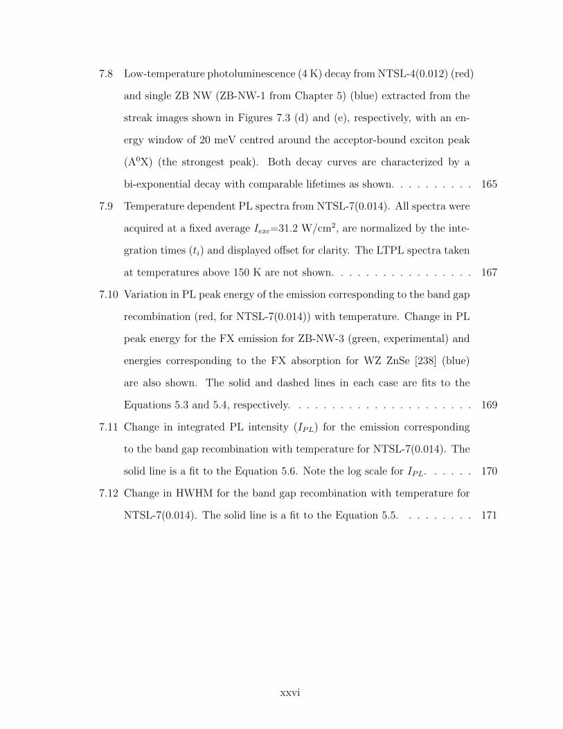
7.8 Low-temperature photoluminescence (4 K) decay from NTSL-4(0.012) (red)
and single ZB NW (ZB-NW-1 from Chapter 5) (blue) extracted from the
streak images shown in Figures 7.3 (d) and (e), respectively, with an en-
ergy window of 20 meV centred around the acceptor-bound exciton peak
(A0X) (the strongest peak). Both decay curves are characterized by a
bi-exponential decay with comparable lifetimes as shown. . . . . . . . . . 165
7.9 Temperature dependent PL spectra from NTSL-7(0.014). All spectra were
acquired at a fixed average Iexc=31.2 W/cm2, are normalized by the inte-
gration times (ti) and displayed offset for clarity. The LTPL spectra taken
at temperatures above 150 K are not shown. . . . . . . . . . . . . . . . . 167
7.10 Variation in PL peak energy of the emission corresponding to the band gap
recombination (red, for NTSL-7(0.014)) with temperature. Change in PL
peak energy for the FX emission for ZB-NW-3 (green, experimental) and
energies corresponding to the FX absorption for WZ ZnSe [238] (blue)
are also shown. The solid and dashed lines in each case are fits to the
Equations 5.3 and 5.4, respectively. . . . . . . . . . . . . . . . . . . . . . 169
7.11 Change in integrated PL intensity (IPL) for the emission corresponding
to the band gap recombination with temperature for NTSL-7(0.014). The
solid line is a fit to the Equation 5.6. Note the log scale for IPL. . . . . . 170
7.12 Change in HWHM for the band gap recombination with temperature for
NTSL-7(0.014). The solid line is a fit to the Equation 5.5. . . . . . . . . 171
xxvi

C.1 (a) Relative positions of donor and acceptor levels in the simplified band
diagram; (b) Radiative and non-radiative transitions: (A) Free exciton
recombination (FX), (B) and (C) radiative recombination of donor- and
acceptor-bound excitons (D0X,A0X), (D) donor-acceptor pair (DAP) re-
combination (D0A0), (E) radiative recombination of a free electron and
a neutral acceptor (eA0), (F) radiative recombination of a free hole and
a neutral donor (D0h), and (G) and (H) are non-radiative transitions of
free electrons and holes to ionized donors and acceptors, respectively. [(b)
adapted from Ref [251]] . . . . . . . . . . . . . . . . . . . . . . . . . . . . 196
D.1 Components and principle of operation of a streak camera . . . . . . . . 212
E.1 First BZ of (a) ZB and (b) WZ crystal lattices [316]. . . . . . . . . . . . 216
E.2 Calculated band structures of ZnSe in (a) ZB and (b) WZ crystal struc-
tures. Reprinted with permission from Ref. [317] © 1994 American Phys-
ical Society. . . . . . . . . . . . . . . . . . . . . . . . . . . . . . . . . . . 217
E.3 Band-structure of ZnSe NTSLs calculated using ab Initio pseudopotential
method within the local density approximation (LDA). The energy bands
of the NH structure are closely related to that of the wurtzite structure
(2H) with bands folded at 2/N(0, 0, 2π/c) along the Γ-A direction. This
can be clearly seen by comparing the band-structures for the 2H (a) and
4H (b), for example. It is noted that there are some important deviations
such as splitting of some degeneracies that cannot be accounted for by
a simple folding. However, the bands near the direct band gap at the Γ
point are very similar in all the structures apart from a gradual shift in the
band gap with N . The horizontal line indicates the position of the valence
band maximum (VBM). Also shown is the calculated band-structure for
6H-polytype (c). . . . . . . . . . . . . . . . . . . . . . . . . . . . . . . . . 219
xxvii
E.4 Comparison of the calculated band-structures for wurtzite (2H) (red) and
4H-polytype (blue) structures. A and A1 denote the Brillouin zone bound-
ary along the growth direction for 2H and 4H structures, respectively. The
band gap for 4H-poytype is reduced compared to that of wurtzite (2H)
structure. The horizontal line (green) indicates the position of the valence
band maximum (VBM). . . . . . . . . . . . . . . . . . . . . . . . . . . . 220
G.1 Structural characterization of ZB-NW-2: (a) Overview TEM micrograph,
and (b) TEM micrograph at a magnification higher than in (a). . . . . . 224
G.2 (a) HR-TEM micrograph from an area of ZB-NW-2, and (b) Indexed FFT
pattern acquired from an area (squared in red) in (a). The viewing direc-
tion for (a) and (b) corresponds to 〈110〉. . . . . . . . . . . . . . . . . . . 224
G.3 (a) HR-TEM micrograph from an area of ZB-NW-2, and (b) Indexed SAD
pattern from a larger area (shown in Figure G.1 (b)) of ZB-NW-2. The
viewing direction for (a) and (b) corresponds to 〈110〉. . . . . . . . . . . 225
G.4 Structural characterization of WZ-NW-2: (a) Overview TEM micrograph,
and (b) TEM micrograph at a magnification higher than in (a). . . . . . 226
G.5 (a) HR-TEM micrograph from an area of WZ-NW-2, (b) Indexed FFT
pattern acquired from an area (squared in red) in (a). The viewing direc-
tion for (a) and (b) is 〈1100〉. . . . . . . . . . . . . . . . . . . . . . . . . 226
G.6 Structural characterization of NTSL-1(0.100): (a) Overview TEM micro-
graph, and (b) HR-TEM micrograph from an area of NTSL-1(0.100). The
viewing direction for (a) and (b) is 〈110〉. . . . . . . . . . . . . . . . . . . 227
G.7 HR-TEM micrograph from an area of NTSL-1(0.100). The periodic twin-
planes as atomically sharp interfaces can be seen. The viewing direction
is 〈110〉. . . . . . . . . . . . . . . . . . . . . . . . . . . . . . . . . . . . . 228
xxviii

G.8 (a) HR-TEM micrograph from an area of NTSL-1(0.100), and (b) Indexed
FFT pattern taken from the area (squared in red) in (a). The viewing
direction is 〈110〉. . . . . . . . . . . . . . . . . . . . . . . . . . . . . . . . 229
G.9 Structural characterization of NTSL-2(0.077): (a) Overview TEM micro-
graph, and (b) HR-TEM micrograph from an area of NTSL-2(0.077). The
viewing direction for (a) and (b) is 〈110〉. . . . . . . . . . . . . . . . . . . 229
G.10 HR-TEM micrograph from an area of NTSL-2(0.077). The viewing direc-
tion is 〈110〉. . . . . . . . . . . . . . . . . . . . . . . . . . . . . . . . . . . 230
G.11 (a) HR-TEM micrograph from an area of NTSL-2(0.077), and (b) Indexed
FFT pattern taken from the area (squared in red) in (a). The viewing
direction is 〈110〉. . . . . . . . . . . . . . . . . . . . . . . . . . . . . . . . 231
G.12 Structural characterization of NTSL-3(0.059): (a) Overview TEM micro-
graph from an area of NTSL-3(0.059), and (b) a HR-TEM micrograph
from an area of NTSL-3(0.059). The viewing direction for (a) and (b) is
〈110〉. . . . . . . . . . . . . . . . . . . . . . . . . . . . . . . . . . . . . . 232
G.13 A composite image of the HR-TEM micrographs of NTSL-3(0.059), taken
at successive locations along its length. . . . . . . . . . . . . . . . . . . . 233
G.14 (a) HR-TEM micrograph from an area of NTSL-3(0.059), and (b) Indexed
FFT pattern taken from the area (squared in red) in (a). The viewing
direction is 〈110〉. . . . . . . . . . . . . . . . . . . . . . . . . . . . . . . . 234
G.15 (a) HR-TEM micrograph from an area of NTSL-3(0.059), and (b) Indexed
SAD pattern from a larger area (shown in Figure G.12 (a)) of NTSL-
3(0.059). The viewing direction for (a) and (b) is 〈110〉. . . . . . . . . . . 235
G.16 Structural characterization of NTSL-4(0.012): (a) Overview TEM micro-
graph from an area of NTSL-4(0.012), and (b) a TEM micrograph from
an area of NTSL-4(0.012), at a magnification higher than in (a) . The
viewing direction for (b) is 〈110〉. . . . . . . . . . . . . . . . . . . . . . . 235
xxix
G.17 (a) HR-TEM micrograph from an area of NTSL-4(0.012), and (b) Indexed
FFT pattern taken from the area (squared in red) in (a). The viewing
direction is 〈110〉. . . . . . . . . . . . . . . . . . . . . . . . . . . . . . . . 236
G.18 (a) HR-TEM micrograph from another area of NTSL-4(0.012), and (b)
Indexed SAD pattern from a larger area of NTSL-4(0.012). The viewing
direction for (a) and (b) corresponds to 〈110〉. . . . . . . . . . . . . . . . 236
G.19 Structural characterization of NTSL-5(0.019): (a) Overview TEM micro-
graph from an area of NTSL-5(0.019), and (b) a HR-TEM micrograph
from an area of NTSL-5(0.019). The viewing direction for (a) and (b) is
〈110〉. . . . . . . . . . . . . . . . . . . . . . . . . . . . . . . . . . . . . . 237
G.20 (a) HR-TEM micrograph from an area of NTSL-5(0.019), and (b) Indexed
FFT pattern taken from the area (squared in red) in (a). The viewing
direction is 〈110〉. . . . . . . . . . . . . . . . . . . . . . . . . . . . . . . . 237
G.21 (a) HR-TEM micrograph from another area of NTSL-5(0.019), and (b)
Indexed SAD pattern from a larger area (shown in Figure G.19 (a)) of
NTSL-5(0.019). The viewing direction for (a) and (b) is 〈110〉. . . . . . . 238
G.22 Structural characterization of NTSL-6(0.333): (a) Overview TEM micro-
graph of NTSL-6(0.333), which extends on both sides of the grid bar la-
belled as shown, and (b) TEM micrograph of NTSL-6(0.333) on the side
labelled ‘Top of the grid bar’. . . . . . . . . . . . . . . . . . . . . . . . . 238
G.23 On the side labelled ‘Below the grid bar’: (a) Overview TEM micrograph
from an area of NTSL-6(0.333), and (b) a HR-TEM micrograph from an
area of NTSL-6(0.333). The viewing direction for (a) and (b) is 〈110〉. . . 239
G.24 On the side labelled ‘Top of the grid bar’: (a) Overview TEM micrograph
from an area of NTSL-6(0.333), and (b) a HR-TEM micrograph from an
area of NTSL-6(0.333). The viewing direction for (a) and (b) is 〈110〉. . . 239
xxx

List of Acronyms
1D One-dimensional
BBO Beta Barium Borate
BEC bound exciton complex
BX Bound exciton
BZ Brillouin Zone
CCD Charge-Coupled Device
CL cathodoluminescence
COV coefficient of variation
CBM conduction band minimum
CVD chemical vapour deposition
DAP Donor-acceptor pair
DL Deep level
ED Electron diffraction
EDS Energy Dispersive X-ray Spectroscopy; see also EDXS
EDXS Energy Dispersive X-ray Spectroscopy; see also EDS
EM Electron microscope (or microscopy); see also SEM, STEM, TEM,
HR-TEM
FCC face-centered cubic
FET Field Effect Transistor
FIB Focused ion beam
FFT Fast-Fourier Transform
FX Free exciton
xxxi

FWHM Full-width at half-maximum
HPD-TA High-Performance Digital Temporal Analyser
HR-TEM High-resolution Transmission Electron Microscope (or Microscopy); see
also SEM, STEM, TEM
HWHM Half-width at half-maximum
LA longitudinal-acoustic
LED Light Emitting Diode; see also BLED
LDA local density approximation
LO longitudinal-optical
LPE liquid-phase epitaxy
LTCL low-temperature cathodoluminescence; see also RTCL
LTPL low-temperature photoluminescence; see also RTPL
MBE Molecular Beam Epitaxy
MOCVD Metal-Organic Chemical Vapor Deposition
NA Numerical aperture
NBE near band-edge
NTSL Nanowire Twinning Superlattice; see also RTNW
NW nanowire
PDF Powder diffraction file
PL photoluminescence
PMT photo-multiplier tube
ppm parts per million
ppb parts per billion
xxxii
QTH quartz-tungsten-halogen
RT room-temperature
RTCL room-temperature cathodoluminescence; see also LTCL
RTNW randomly twinned nanowire; see also NTSL
RTPL room-temperature photoluminescence; see also LTPL
SA Self-activated
SAD selected-area diffraction pattern
s.d. standard deviation
s.e.m. standard error in mean
SHG Second Harmonic Generator
SNW Single Nanowire
SEM Scanning Electron Microscope (or Microscopy); see also STEM, TEM,
HR-TEM
SNR signal-to-noise ratio
STEM Scanning and Transmission Electron Microscope (or Microscopy); see
also SEM, TEM, HR-TEM
SX Surface exciton
TA transverse-acoustic
TO transverse-optical
TEM Transmission Electron Microscope (or Microscopy); see also SEM,
STEM, HR-TEM
TRPL Time-resolved photoluminescence
TSL Twinning Superlattice; see also NTSL
VBM valence band maximum
xxxiii

VLS Vapor-Liquid-Solid
VND Variable Neutral Density
UV ultra-violet
WZ Wurtzite
XPS X-ray photoemission spectroscopy
XRD X-ray diffraction
ZB Zinc-blende
ZB-WZ Zinc-blende-wurtzite
ZPL zero-phonon line
xxxiv
List of Symbols
α a fitting parameter in Equation 5.3, representing dEg/dT at high temperatures
αB strength of the exciton (electon)-average pnohon interaction in Equation 5.4
β a fitting parameter in Equation 5.3 considered to be equivalent to θD
χ2-test a statistical test to compare the observed experimental data with that expected
from a model
∆µ standard error in mean (s.e.m.) in the distribution of individual segment widths
of NTSLs
∆d dispersion in d, (s.d.) (=σ)
δd error in d, (s.e.m.) (=∆µ)
ε dielectric constant
η efficiency of PL emission
γ Periodicity parameter used to characterize the twin-plane spacing d in NTSLs
Γ-point centre of the Brillouin zone (BZ) with k=0
Γp linewidths of luminescence peaks in terms of the full-width at half-maximum
(FWHM)
Γimp a parameter in Equation C.24 representing contribution to linewidths due to scat-
tering by fully ionized impurities
Γinh a parameter representing inhomogeneous broadening in Equation 5.5
xxxv
ΓLO a parameter in Equation 5.5 representing the strength of the exciton (electron)-LO
phonon interaction
γth a parameter in Equation 5.5 representing the strength of the exciton (electron)-
acoustic phonon interaction
~ωLO energy of the LO-phonon replica
~ reduced Planck’s constant=h/2π=6.58212 ×10−16 eV.sec
B notation for a twin-plane in NTSLs
µ mean of the distribution of individual segment widths of NTSLs
σ standard deviation of the distribution of individual segment widths of NTSLs
τ PL lifetime
τ1, τ2 PL lifetimes in bi-exponential decay processes
τAX ,τnrAX radiative and non-radiative lifetimes of acceptor-bound excitons
τDX ,τnrDX radiative and non-radiative lifetimes of donor-bound excitons
τFX ,τnrFX radiative and non-radiative lifetimes of free excitons
θB temperature corresponding to an average phonon energy in Equation 5.4
θD Debye temperature for a crystal
θLO temperature corresponding to LO-phonon energy
a lattice constant of a material in ZB crystal structure
a′, b′, ..., l′ coefficients in the Equation C.14
A− ionized acceptor
A−X excitons bound to ionized acceptors
A0 neutral acceptor
A0X excitons bound to neutral acceptors
xxxvi
aB exciton Bohr radius
aGaAs lattice constant of GaAs
avdW effective van der Waals coefficient for the interaction between a neutral donor and
a neutral acceptor
aZnSe lattice constant of ZnSe (in zinc-blende crystal structure)
AsSe As atom on the site of a Se atom in ZnSe
C,C1, C2 coefficients in Equations C.30 and C.31
CuZn substitutional Cu atom on the site of a Zn atom in ZnSe
d Twin-plane spacing (or) the distance between successive twin-planes in NTSLs
D+ ionized donor
D+X excitons bound to ionized donors
D0 neutral donor
D0X excitons bound to neutral donors
D0h donor-to-hole transition
df ilm film thickness
d<111> The interplanar spacing in the 〈111〉 direction in ZB-ZnSe
dslit Slit-width of the spectrometer
e electronic charge
E(r) term representing Coulombic interaction energy between a donor and an acceptor
e− an electron
EA ionization energy of an acceptor
Ea thermal activation energy for a non-radiative recombination process
EB Coulombic interaction energy between a donor and an acceptor separated by RB.
xxxvii

ED ionization energy of a donor
Eg electronic energy band gap
Ek is the kinetic energy of the free electron (=kBT )
Em energy of emitted photons in a DAP-related recombination
Ep energy position of a PL peak in a PL spectrum
Ex notation for the free exciton emission used in the literature
Ea1, Ea2 thermal activation energies for non-radiative recombination processes, subscripts
denote different mechanisms
EBX binding energy of the exciton bound to donors or acceptors
EDAP (r) energy position of the DAP emission, a function of the distance r between
associated donor and acceptor
EDL energy position of the deep-level emission band in the RTPL spectrum of ZnSe
nanostructures
EFB energy position of PL peak related to free-to-bound transitions
EFX binding energy of free excitons
Eg,WZ Eg of ZnSe in the WZ crystal structure
Eg,ZB Eg of ZnSe in the ZB crystal structure
Eimp average binding energy of the impurities in Equation C.24
ENBE energy position of the near band -edge peaks in the RTPL spectrum of ZnSe
nanostructures
Eph energy of photons of light
eA0 electron-to-acceptor transition
GaZn Ga atom on the site of a Zn atom in ZnSe
h Planck’s constant=4.13567 ×10⁻¹⁵ eV.sec
xxxviii

hνB emitted photon energy of a DAP separated by a shallow impurity Bohr radius
hνm emission band peak energy in a DAP recombination (=Em)
hν∞ photon energy corresponding to infinitely distant donor-acceptor pair in Equa-
tion 4.3
hνBE,m energy position of the m-th order phonon-replica of the bound exciton emission
hνBE energy position of the bound exciton emission
hνDAP energy position of the DAP emission
hνFX,m energy position of the m-th order phonon-replica of the free exciton emission
hνFX energy position of the free exciton emission
h+ a hole
i index used to represent NTSLs
I − VZn deep centre in I-doped ZnSe related to VZn and I
I1 notation for PL lines related to neutral acceptor bound excitons
I∗Ag1 notation for a PL line related to excitons bound to AgiAgZn acceptor complex.
see Table B.3
Id′
1 notation for a PL line related to excitons bound to (VZn-complex) deep neutral
acceptors related
Ideep1 , Id1 notation for PL lines related to excitons bound to deep neutral acceptors
I2 notation for PL lines related to neutral donor bound excitons
Ih2 notation for a PL line due to excitons bound to ionized acceptors in the wurtzite
crystal structure, see Table B.3
I∗2 alternate notation for a donor-bound exciton
Im integrated intensity of the m-th order phonon-replica
Ix notation for a PL line at 2.795 eV in ZnSe
xxxix

IY integrated PL intensity of the D0X-line
ID0X integrated PL intensity of the Y-line
Iexc,0 a constant of proportionality in Equation 4.3
Iexc excitation intensity (for excitation of PL)
IPL integrated PL intensity for a PL peak in the PL spectrum
k wave-vector related to the direction of motion of an electron in the crystal
kB Boltzmann constant=8.61733 ×10⁻⁵ eV/K
m order of the phonon-replica
m∗ effective mass of a carrier (electron or hole)
m∗e electron effective mass
m∗h hole effective mass
m∗r reduced effective mass of the free excitons
N Number of monolayers between successive twin-planes in NTSLs
NA concentration of acceptors
ND concentration of donors
NS sample size in the distribution of individual segment widths of NTSLs
NA0 concentration of neutral acceptors
nAX concentration of acceptor-bound excitons
ND0 concentration of neutral donors
nDX concentration of donor-bound excitons
nFE concentration of free excitons
nFX principal quantum number of the excited states of the free excitons
NLO Bose-Einstein statistical factor
xl

Nph average number of phonons emitted in simultaneous emission of photons and
phonons in a transition
p coefficient in the power law relation between IPL and Iexc (Equation C.20)
Pr probability of a radiative transition
Pnr,0, Pnr1,0, Pnr2,0 prefactors in Equations C.26 and C.31
Pnr1, Pnr2 probabilities of non-radiative transitions, subscripts denote different mecha-
nisms
Pnr probability of a non-radiative transition
R volume fraction of ZnSe NWs on ZnSe epilayers
r separation between donors and acceptors associated with a DAP recombination
RB shallow impurity Bohr radius
RH Bohr radius for hydrogen
RY ratio of the integrated PL intensities of the D0X and the Y-line (=ID0X/IY )
Sei Interstitial Se atom
SeZn Antisite defect with a Se atom in place of a Zn atom
T Temperature
ti integration time used in the acquisition of a PL spectrum
Vepi total volume excited by the laser beam of ZnSe epilayers
Vnw total volume excited by the laser beam of ZnSe NWs
VSe Vacancies of Se
V xSe alternate notation for neutral Se vacancies
VZn Vacancies of Zn
VZn/GaZn complex defect centre in ZnSe related to VZn and GaZn
xli

Y emission band in ZnSe related to structural defects
Zni Interstitial Zn atom
ZnSe Antisite defect with a Zn atom in place of a Se atom
ABC atomic planes in the stacking sequence in crystals, each letter denotes a bilayer
xlii

Glossary of terms
acoustic phonons: modes of lattice vibrations in crystals composed of more than one
atoms, where nearby atoms of different kinds vibrate in the same direction with a
periodically varying amplitude
anti-site defect: a type of point defect in compounds when atoms of different elements
exchange their lattice positions, e.g., a Zn atom on a site of Se atom in ZnSe (ZnSe)
binary compound semiconductors: compound semiconductors consisting of two
elements only
Brillouin zone: the wavevector (k) values for a particular energy band are said to
form a Brillouin zone
excitons: a quasi-particle of an electron-hole pair bound by Coulomb interaction
interstitials: a type of point defect where a crystal contains an extra atom at a position
which is not a regular lattice site
longitudinal (LO and LA) phonons: phonons with atomic displacements parallel
to the propagation direction. These generally have higher energy (compared to the
transverse phonons)
native point defects: point defects that involve atoms of the elements forming the
crystal, so called to distinguish from point defects that involve foreign impurities
optical phonons: modes of lattice vibrations in crystals composed of more than one
atoms, where nearby atoms of different kinds vibrate in opposite directions with
amplitudes that are inversely proportional to the atomic masses
xliii
phonon-replicas: subsidiary peaks in a PL spectrum which are a result of simultaneous
emission of a photon and a phonon. These are equally spaced with separation energy
equal to the phonon energy
phonons: collective vibrational modes of the atoms forming a crystal. These modes are
quantized where each quanta of lattice vibrations corresponds to a phonon energy
planar defects: a disruption in a homogeneous material that extends across a plane,
e.g., a stacking fault
point defect: crystallographic defects in a crystal which extend only a few interatomic
distances in any direction (or) defects localized at or around one lattice site only
in a crystal
polytypes: different modifications of a material which are chemically identical but
differ in atomic arrangement
rotation twin-plane: in a frequently occurring mode of twinning where one domain
of the crystal is a mirror image of the other part of the crystal along a certain
crystallographic plane called as twin-plane. A rotation twin-plane involves the
rotation of two domains of the crystal by 60◦ or its odd multiples
stacking faults: a type of planar defect, which is an interruption of one or more layers
in the stacking sequence of atomic planes in crystals
transverse (LA and TA) phonons: phonons with atomic displacements perpendic-
ular to the propagation direction. These generally have lower energy (compared to
the longitudinal phonons)
twinning: twinning refers to the occurrence of more than one domains in a crystal which
are oriented with respect to each other according to some symmetrical relationship
xliv

substitutional impurity: a type of point defect where atoms of foreign elements
replace an atom in the host lattice, e.g. GaZn where Ga replaces a Zn atom
vacancies: a type of point defect in which an atom is missing from a lattice site
xlv

Chapter 1
Background-Current state of the art
1.1 Introduction
1.1.1 II-VI compound semiconductors
II-VI compounds are formed from the elements of group II and VI of the periodic table.
They include sulphides, selenides, tellurides and oxides of zinc (Zn), cadmium (Cd),
mercury (Hg) and alkaline earth metals, and their alloys. II-VI semiconductors such as
CdS, CdSe, CdTe, ZnO, ZnS, ZnSe, ZnTe possess wide direct band gaps, Eg, with the
minima of the conduction band and maxima of the valence band occurring at the Γ-point
(k=0), the centre of the Brillouin zone (BZ). The band structure notation is described
in Appendix E. While there is no formal definition of ”wide band gap”, a semiconductor
may be referred to as having a wide band gap if Eg is about twice or three times that
of Si, the most commonly used semiconductor Si [1], with Eg=1.1 eV [2]. Neumark
somewhat arbitrarily specifies wide band gap as an energy gap exceeding ∼1.5 eV [3],
and this definition of wide band gap is implied in this thesis. Materials other than II-
VI compounds may also possess wide band gaps. For example, GaN (Eg,GaN= 3.39 eV
at room-temperature (RT) [2]) from the III-V family of compounds and SiC (Eg,SiC=
2.9 eV at RT [2]) with an indirect band gap are among the prominently studied wide
1

Chapter 1. Background 2
band gap semiconductors. In an indirect band gap semiconductor, band extrema occur at
different k’s in the BZ. Applications of SiC, GaN and ZnSe in devices have been reviewed
by Morkoc et al. [2], while recent progress in their application towards ultra-violet (UV)
photodetection have been reviewed by Monroy et al. [4]. Wide band gap II-VI compound
semiconductors have been a subject of intense research during the last three decades,
which can be attributed to their promising optical and electronic properties [5–7]. They
have attracted much attention as prospective UV and visible LED (light-emitting diode)
materials owing to their excellent luminescence properties. Progress towards realization
of luminescent devices based on II-VI compounds has been reviewed by Park et al. [8]
and Aven et al. [9], among others.
1.1.2 ZnSe for opto-electronic devices
ZnSe is a typical wide band gap compound semiconductor with a direct band gap of
2.7 eV at RT [6, 7] and corresponding band-edge separation (of the band extrema) in
the blue spectral region. ZnSe is considered an excellent optical material for blue lasers
and optical devices in the short wavelength range [2, 5, 6, 8, 9]. Another advantage of
using ZnSe in device applications is its complete miscibility with other group II and VI
elements which allow for alloy compounds [10, 11]. ZnSe has a zinc-blende (ZB) crystal
structure [5] which consists of two inter-penetrating face-centred cubic (FCC) lattices,
which are offset by a quarter of the unit cell body-diagonal [12]. ZnSe also occurs in
the Wurtzite (WZ) crystal structure which is meta-stable (for ZnSe) at RT [13]. For
device fabrication using ZnSe, one of the important requirements is the realization of p-n
junctions based on ZnSe, which requires successful incorporation of both n- and p- type
impurities in the semiconductor. ZnSe may easily be doped n-type, but not p-type [2,
8, 9, 14]. In the past, ZnSe faced problems of low purity and strong self-compensation,
and fabrication of p-n junctions used to be very difficult [5, 8]. With the advancements
in the growth techniques such as metal-organic chemical vapour deposition (MOCVD)
Chapter 1. Background 3
and molecular beam epitaxy (MBE), growth of high-purity ZnSe became feasible. At the
same time, continued research led to the possibility of p-type doping [5]. Applications of
ZnSe in optoelectronic devices have been discussed previously [2, 4–6, 8, 9] while Luo et
al. [15] and Kolodzieski et al. [16] have focused exclusively on developments in the area
of ZnSe-based laser-diodes. Characterization of II-VI compound semiconductors in the
past relied heavily upon the techniques of optical spectroscopy such as luminescence [14],
which in simple terms is the emission of light by a material under laser excitation. In
fact, most of the fundamental optical processes were first identified and studied in II-VI
compounds, and later recognized in other materials [14]. A brief overview of luminescence
spectroscopy applied to ZnSe single crystals and epilayers is given in Section 1.5. The
epilayers here refer to ZnSe layers grown on a crystalline substrate with a lattice constant
closely matched to that of ZnSe. The substrate for growth of ZnSe epilayers has mostly
been GaAs [2, 7].
1.2 Semiconductor nanowires
The last decade has seen an upsurge of interest in the growth, characterization and
technological applications of one-dimensional (1D) structures made of a wide variety of
materials [17]. Depending on their dimensions and the particular material, the motion
of carriers may be confined in two directions in such 1D structures while the third is
unconfined and capable of electrical conduction. In such cases, structures typically will
have nanometer scale confining dimensions and micron scale lengths, corresponding to
large aspect ratios. These 1D structures are thus called 1D-nanostructures, and are
commonly referred to as nanowires, nanoribbons, nanobelts, nanotubes etc based on
their particular geometry. 1D nanostructures of various II-VI [18] and III-V [19] binary
compound semiconductors, metallic and semiconducting elements (e.g. Ag [20], Si [21,
22]) and other inorganic compounds (e.g. SnO2 [23]) have been synthesized. An overview

Chapter 1. Background 4
of nanowire synthesis is given in Section 1.4. Interest in such 1D nanostructures follows
the trend towards miniaturization of opto-electronic devices [24], and the fact that current
lithographic patterning technology for miniaturization is reaching its limits. It is believed
that 1D-nanostructures, henceforth termed as nanowires (NWs) are ideal candidates for
exploiting the dependence of electrical, optical and mechanical properties on reduced
dimensionality [24,25]. The electrical and optical properties of semiconductor NWs may
be significantly affected by quantum confinement, whereby the energy band gap of a
semiconductor increases as NW diameter reduces [25]. Since the developments in research
on NWs has occurred concurrently for a large variety of materials, the current literature
on NWs is vast and beyond the scope of this thesis. Yang et al. [26] provided a critical
view of the progress in the past decade of research on NWs. The following are a few
important areas where NWs have shown promise for practical and commercially viable
applications: biological sensors [27–29], chemical sensors [30], NW photonics [31], nano-
electronics [17,32–34], NW photovoltaics [35,36], photodetectors [37], and thermoelectric
applications [38–40]. Due to their small size, NWs also find applications in unconventional
areas where bulk crystals and thin-film structures cannot be efficiently used, e.g., single
cell endoscopy [41] and drug delivery to target cells inside living body [42].
An important application based on the optical response of semiconductor NWs is in
single-NW (SNW) lasers. This is based on the salient characteristics of NWs such as their
single-crystalline structure, high index of refraction and smooth surfaces, which allow
their end-facets to serve as partial mirrors, forming a so-called Fabry-Perot cavity. The
NW itself acts as an optical gain medium. SNW lasers based on GaN [43] and ZnO [44]
NWs have been demonstrated, while a ZnO nanolaser based on electrical injection was
realized recently [45]. In fact, NW-based nanolasers have become an established sub-field
of study, with reviews by Mariano et al. [46], Ning [47] and Vanmaekelbergh et al. [48].
Chapter 1. Background 5
1.2.1 ZnSe nanowires
There have been considerable advances in the growth of II-VI compound semiconductor
NWs [18], with the majority of the work focussed on ZnO [44,49,50], ZnS [51], CdSe [52],
CdS [53,54] and ZnSe [55]. ZnSe NWs have been extensively studied with a large number
of works devoted to their synthesis and structural characterization. Section 1.6.2 presents
a survey of optical studies of ZnSe NWs [55–120] aimed at understanding their optical
properties. Demonstrated applications of ZnSe NWs include photo-detectors [71, 121],
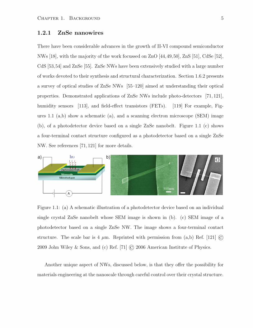
humidity sensors [113], and field-effect transistors (FETs). [119] For example, Fig-
ures 1.1 (a,b) show a schematic (a), and a scanning electron microscope (SEM) image
(b), of a photodetector device based on a single ZnSe nanobelt. Figure 1.1 (c) shows
a four-terminal contact structure configured as a photodetector based on a single ZnSe
NW. See references [71,121] for more details.
c)
Figure 1.1: (a) A schematic illustration of a photodetector device based on an individual
single crystal ZnSe nanobelt whose SEM image is shown in (b). (c) SEM image of a
photodetector based on a single ZnSe NW. The image shows a four-terminal contact
structure. The scale bar is 4 µm. Reprinted with permission from (a,b) Ref. [121] ©
2009 John Wiley & Sons, and (c) Ref. [71] © 2006 American Institute of Physics.
Another unique aspect of NWs, discussed below, is that they offer the possibility for
materials engineering at the nanoscale through careful control over their crystal structure.
Chapter 1. Background 6
1.3 Semiconductor nanowire heterostructures
Significant progress has been made in the field of NWs in general, both fundamentally
and technologically. This has led to further developments, which are hitherto not pos-
sible on bulk crystals, epilayers or nanoparticles. One of the emerging areas is that of
crystal structure engineering [122,123]. This is based on a precise control over the crystal
structure, and realization of heterostructures with desired properties. A semiconductor
heterostructure means a structure composed of two or more different semiconductors with
different Eg’s, which may arise due to modulations in composition (e.g., due to differ-
ent materials or alloying), crystal structures (e.g. ZB or WZ), or strain. A periodically
modulated heterostructure is also called a superlattice. Considerable and remarkable
progress has been made in the area of crystal structure engineering in III-V compound
semiconductor NWs, a few examples of which include control over design of ZB-WZ
superlattices [124, 125], quantum dots defined by alternate crystal structures precisely
placed in NWs [126], and precisely controlled semiconductor heterostructures [127]. Fur-
ther details on these developments may be found in a recent review by Caroff et al. [122].
It may be noted that the optical and electronic properties of these crystal structure en-
gineered heterostructures are not fully understood yet, which is reasonable given that
the success in their fabrication has been recent. This progress in crystal structure engi-
neering has almost eluded II-VI semiconductor NWs where such studies have not been
reported thus far. However, II-VI compounds being miscible in each other are excellent
for compositional NW heterostructures and superlattices, and have been exploited aptly
towards the synthesis of these structures. The progress in band gap modulation based on
compositional engineering of NWs has been summarized by Pan et al. [128] and Zhuang
et al. [129]. The optical properties of compositional NW heterostructures have been stud-
ied and expectedly resemble those of bulk alloys and conventional heterostructures. An
important issue adversely affecting the optical properties of alloys has been the disorder
introduced by alloy fluctuations and alloy scattering. The crystal potential in alloys is

Chapter 1. Background 7
perturbed as a result of the microscopic and statistical variations of the alloy composi-
tion. These variations strongly affect the linewidths of luminescence lines. A detailed
discussion on this can be found in a review by Pavesi et al. [130]. A new kind of structure
unique to NWs, called a Nanowire Twinning Superlattice (NTSL) was observed earlier
[104,131], and will be discussed in more detail in the next section.
1.3.1 Nanowire Twinning Superlattices (NTSLs)
A Nanowire Twinning Superlattice (NTSL) is composed of periodically arranged rotation
twin-planes in a NW along its length. A rotation twin-plane in a ZB crystal involves
rotation of two domains of a crystal with respect to each other. A NTSL is composed
of a series of periodic rotation twin-planes, each of which separate two domains of NWs
rotated with respect to each other by 60◦ or odd multiples thereof. Figures 1.2 (a-c) show
Transmission Electron Microscope (TEM) images of NTSLs realized on InP NWs, while
(d) shows a InAs NW with periodic twin-planes. Figure 1.2 (e) shows an atomic model
of a section of a NTSL with the locations of rotation twin-planes shown by arrows. The
twin-plane spacing or twin-periodicity d, is defined as the spacing between two consecutive
twin-planes. This is shown as the distance between the planes marked by A and C in
Figure 1.2 (e). The structure of a NTSL can be considered as follows. The bonds in the
〈111〉-direction in a NW crystal are cut, and one half of the crystal is rotated by 60◦ about
the bond axis. All the bonds in the two halves of the crystal are then reconnected after the
rotation. The rotation twin-planes are coherent defect-free interfaces. This means that
there is no change in the composition at a twin-plane and no strain is induced because
all the original bonds, bond lengths and bond angles are preserved. Therefore, NTSLs
are compositionally uniform and fully strain-relaxed superlattices. Strictly speaking, a
NTSL is not a heterostructure because there is no variation in composition or crystal
structure along its length, and consequently neither of its band gap. The implications of
periodic rotation twin-planes in NTSLs can be understood as follows.
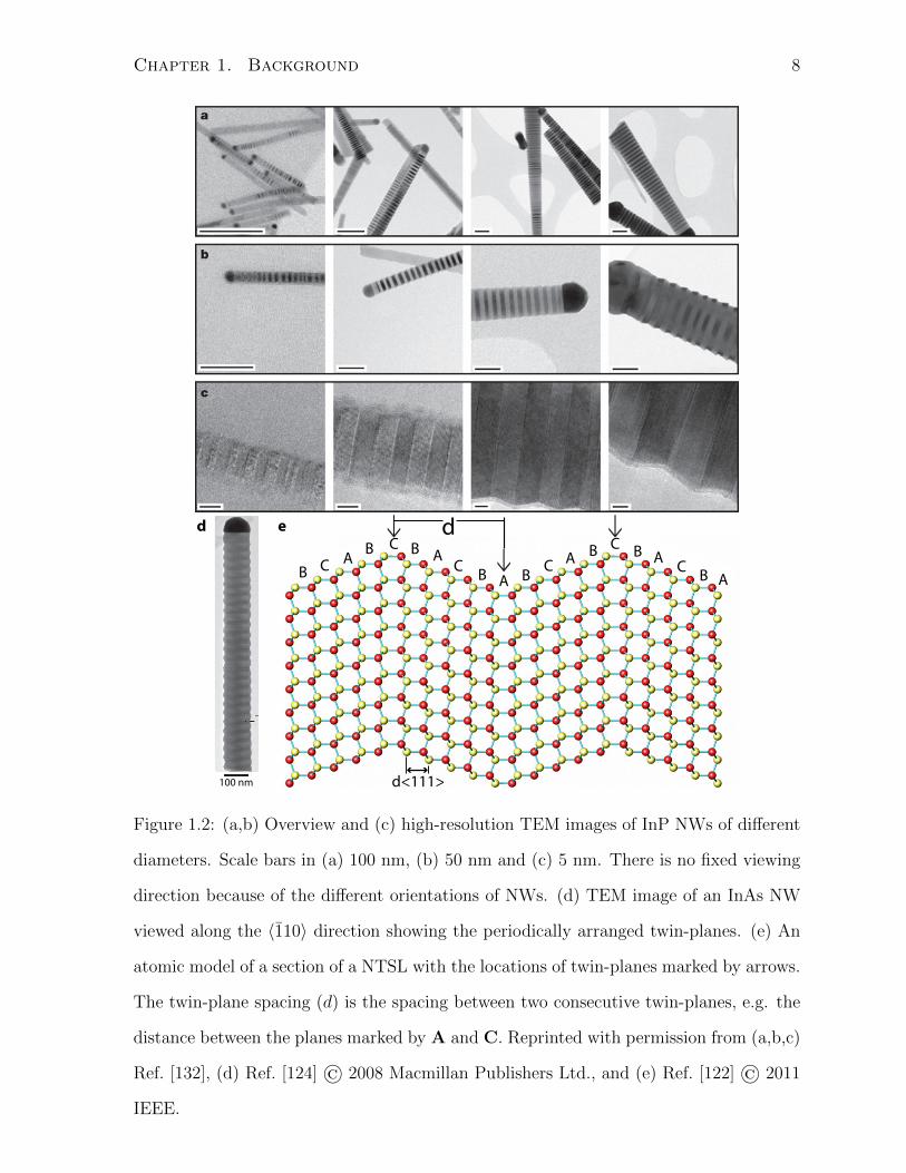
Chapter 1. Background 8
d e
B C AB C B A
C B A B C A B C B A C B A
100 nm
d
d<111>
Figure 1.2: (a,b) Overview and (c) high-resolution TEM images of InP NWs of different
diameters. Scale bars in (a) 100 nm, (b) 50 nm and (c) 5 nm. There is no fixed viewing
direction because of the different orientations of NWs. (d) TEM image of an InAs NW
viewed along the 〈110〉 direction showing the periodically arranged twin-planes. (e) An
atomic model of a section of a NTSL with the locations of twin-planes marked by arrows.
The twin-plane spacing (d) is the spacing between two consecutive twin-planes, e.g. the
distance between the planes marked by A and C. Reprinted with permission from (a,b,c)
Ref. [132], (d) Ref. [124] © 2008 Macmillan Publishers Ltd., and (e) Ref. [122] © 2011
IEEE.
Chapter 1. Background 9
In binary compound semiconductors with a ZB crystal structure, a pair of atoms
of the two elements defines one layer in the stacking sequence, also called a bilayer.
The stacking sequence (or the arrangement) of atomic planes for a material with a ZB
crystal structure is ...ABCABC..., while for a material with a wurtzite (WZ) crystal
structure, the sequence is ...ABAB..., where each letter represents a bilayer. In a
ZB material, the stacking sequence is reversed (...ABCABACBA...) at a rotation-
twin-plane (denoted by B). See Figure 1.2 (e) for an atomic model of a section of a
NTSLs where twin-planes C, A and C are marked by an arrow, and the twin-plane
spacing (d) is shown as the distance between planes C and A. Many authors believe
that the ABA sequence around the twin-plane in NTSLs constitutes one monolayer of
the WZ material [132, 133]. They consider NTSLs as ZB-WZ superlattices consisting of
alternating regions of the ZB and WZ material. Caroff et al. [122,124] on the other hand
have stated that two consecutive twin-planes (i.e. ...ABCABABC...) are required to
define a segment of the WZ structure (ABAB), with a minimum of four bilayers. They
maintained that a single twin-plane does not define a layer of the WZ material, and
postulated that the NTSLs with periodic twin-planes can be considered as polytypes
of the parent material. A polytype refers to the different forms of a material which
are identical in chemical composition but differ in their crystalline arrangements, and
ZB-WZ polytypism is probably the most common example [134]. This means that for
materials which exist in ZB and WZ crystal structures, their NTSLs would have an
intermediate character in terms of their physical properties. Various terms have been
used in the literature to refer to NTSLs including periodically twinned NWs [131, 135],
twinning modulations [77], periodically faceted NWs [136], twin-plane superlattices [124]
and twinning superlattices [132], but they all refer to the same class of structures. The
use of the term ‘NTSL’ is specific to this thesis.
Twinning Superlattices (TSLs) were predicted to exist [137] and possess unusual elec-
tronic and optical properties, including a direct Eg in indirect Eg semiconductors such
Chapter 1. Background 10
as Ge and GaP [137,138]. NTSLs possess long-range order in one dimension (the growth
direction) with periodic atomically sharp interfaces. The issues of alloying and strain
encountered in conventional heterostructured superlattices which adversely affect their
optical properties are avoided in NTSLs. They are also expected to lead to interesting
phenomena including miniband formation [122, 138] with clear advantages such as be-
ing chemically simpler (composed of one compound only) and suitable for cost-effective
fabrication. NTSLs are much more versatile than polytypic (WZ-ZB) and compositional
superlattices, as a wider variety of materials exhibit twinning than those that show poly-
typism or lattice compatibility. Further, synthesis of NTSLs can also be achieved in an
inexpensive natural self-organized way. NTSLs are interesting for thermoelectric appli-
cations as well since the side-facets resulting from periodic twinning (see Figure 1.2 (d),
for example) lead to phonon back-scattering, as shown by recent experiments [139] on
randomly twinned InAs NWs, and simulations [136] for Si NWs. NTSLs are therefore
promising new structures for materials engineering at the nanoscale. NTSLs are unar-
guably among the least studied structures (among NWs) for their fundamental optical
and electronic properties. NTSLs are revisited in Section 2.2 in Chapter 2 where this
lack of understanding of their fundamental properties is discussed in detail.
1.4 Growth of semiconductor nanowires
The growth of 1D structures has been observed for more than 50 years [140], and these
were referred to as whiskers in the past as opposed to the currently used term NWs.
Later, Westwater et al. [141] and Duan et al. [142] renewed the interest in NWs with
demonstrations of the growth of semiconductor NWs using vapour-liquid-solid (VLS)
growth mechanism. A wide variety of growth techniques have been used in the synthesis
of NWs. These techniques have met with varying degrees of success in control over the
growth of NWs. A general overview of these strategies has been given by Dresselhaus
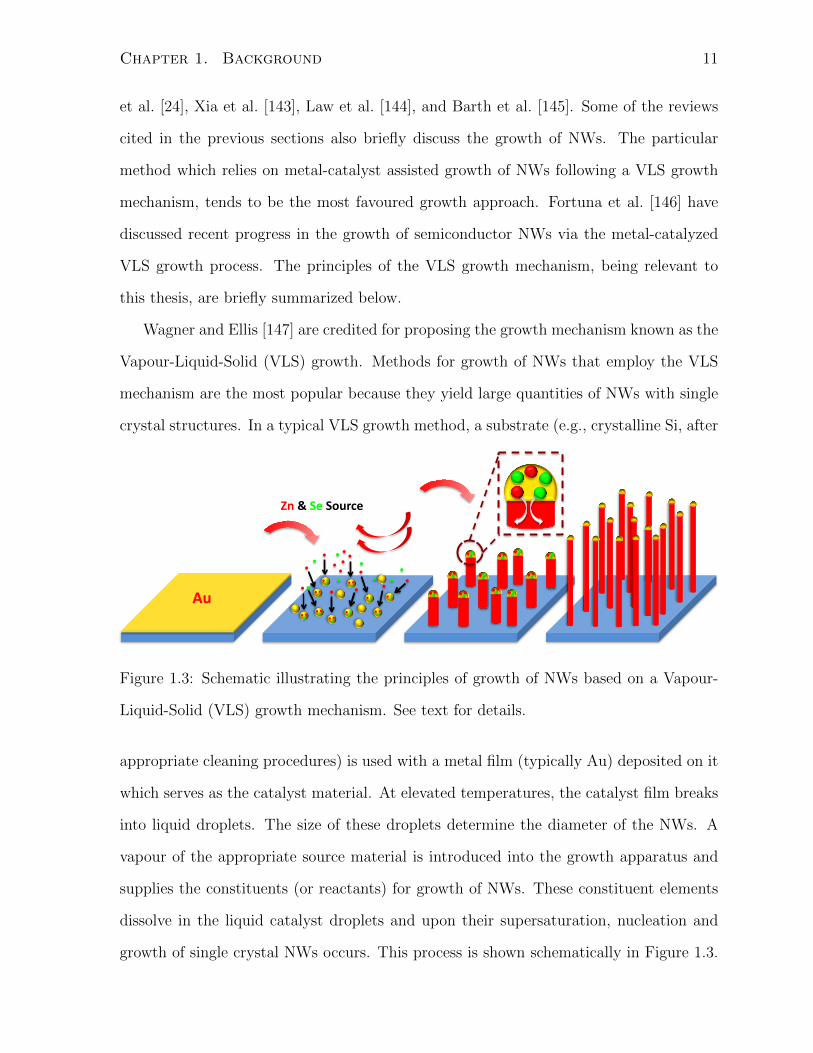
Chapter 1. Background 11
et al. [24], Xia et al. [143], Law et al. [144], and Barth et al. [145]. Some of the reviews
cited in the previous sections also briefly discuss the growth of NWs. The particular
method which relies on metal-catalyst assisted growth of NWs following a VLS growth
mechanism, tends to be the most favoured growth approach. Fortuna et al. [146] have
discussed recent progress in the growth of semiconductor NWs via the metal-catalyzed
VLS growth process. The principles of the VLS growth mechanism, being relevant to
this thesis, are briefly summarized below.
Wagner and Ellis [147] are credited for proposing the growth mechanism known as the
Vapour-Liquid-Solid (VLS) growth. Methods for growth of NWs that employ the VLS
mechanism are the most popular because they yield large quantities of NWs with single
crystal structures. In a typical VLS growth method, a substrate (e.g., crystalline Si, after
Au#
Zn#&#Se#Source#
Figure 1.3: Schematic illustrating the principles of growth of NWs based on a Vapour-
Liquid-Solid (VLS) growth mechanism. See text for details.
appropriate cleaning procedures) is used with a metal film (typically Au) deposited on it
which serves as the catalyst material. At elevated temperatures, the catalyst film breaks
into liquid droplets. The size of these droplets determine the diameter of the NWs. A
vapour of the appropriate source material is introduced into the growth apparatus and
supplies the constituents (or reactants) for growth of NWs. These constituent elements
dissolve in the liquid catalyst droplets and upon their supersaturation, nucleation and
growth of single crystal NWs occurs. This process is shown schematically in Figure 1.3.
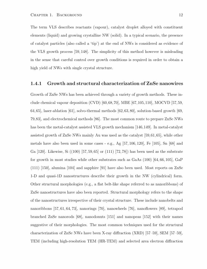
Chapter 1. Background 12
The term VLS describes reactants (vapour), catalyst droplet alloyed with constituent
elements (liquid) and growing crystalline NW (solid). In a typical scenario, the presence
of catalyst particles (also called a ‘tip’) at the end of NWs is considered as evidence of
the VLS growth process [59, 148]. The simplicity of this method however is misleading
in the sense that careful control over growth conditions is required in order to obtain a
high yield of NWs with single crystal structure.
1.4.1 Growth and structural characterization of ZnSe nanowires
Growth of ZnSe NWs has been achieved through a variety of growth methods. These in-
clude chemical vapour deposition (CVD) [60,68,70], MBE [67,105,110], MOCVD [57,59,
64, 65], laser-ablation [61], solvo-thermal methods [62, 63,80], solution-based growth [69,
79,83], and electrochemical methods [86]. The most common route to prepare ZnSe NWs
has been the metal-catalyst assisted VLS growth mechanism [146,149]. In metal-catalyst
assisted growth of ZnSe NWs mainly Au was used as the catalyst [59,61,65], while other
metals have also been used in some cases - e.g., Ag [57, 106, 120], Fe [105], Sn [68] and
Ga [120]. Likewise, Si ((100) [57,59,65] or (111) [72,78]) has been used as the substrate
for growth in most studies while other substrates such as GaAs (100) [64, 66, 105], GaP
(111) [150], alumina [104] and sapphire [91] have also been used. Most reports on ZnSe
1-D and quasi-1D nanostructures describe their growth in the NW (cylindrical) form.
Other structural morphologies (e.g., a flat belt-like shape referred to as nanoribbons) of
ZnSe nanostructures have also been reported. Structural morphology refers to the shape
of the nanostructures irrespective of their crystal structure. These include nanobelts and
nanoribbons [57, 61, 64, 73], nanorings [70], nanowheels [76], nanoflowers [89], tetrapod
branched ZnSe nanorods [68], nanodonuts [151] and nanopeas [152] with their names
suggestive of their morphologies. The most common techniques used for the structural
characterization of ZnSe NWs have been X-ray diffraction (XRD) [57–59], SEM [57–59],
TEM (including high-resolution TEM (HR-TEM) and selected area electron diffraction

Chapter 1. Background 13
(SAD)) [56–59]. Compositional analysis has been mainly carried out using energy disper-
sive X-ray spectroscopy (EDXS or EDS) [56–59], with X-ray photoemission spectroscopy
(XPS) [63] also being used in certain cases, especially for doped ZnSe NWs [80]. These
references are only a few examples of the use of these structural characterization tech-
niques, while one or more of them have been used in almost all reports. ZnSe NWs
with single crystal structure may be termed as homogeneous NWs, indicating uniform
microstructure throughout their length.
1.5 Luminescence characterization of ZnSe single crys-
tals and thin films
Luminescence spectroscopy has been the primary method of optical characterization of
most II-VI compound semiconductors in the past, including ZnSe. The reasons for
this will become apparent in Section 3.2. The principles of photoluminescence (PL)
spectroscopy are described in Appendix C.1, along with the related concepts of opti-
cal transitions which invariably involve excitons, donor-acceptor pairs (DAP), phonons
(longitudinal optical (LO) and transverse acoustic (TA)), and phonon-replicas. In brief,
PL involves the excitation of a semiconductor by light with photon energy equal to or
greater than the Eg of the semiconductor. The electron-hole pairs are created as a result
of this excitation, and recombine radiatively via different processes, e.g., excitonic and
DAP-related. The energy of the emitted photons depends on the recombination process
involved. The resulting PL spectrum provides a finger-print of the impurities in the semi-
conductor and is used for their identification. PL studies on ZnSe crystals date back to
the work performed by Bube et al. [153]. The first detailed study of low-temperature pho-
toluminescence (LTPL) from ZnSe single crystals was reported by Reynolds et al. [154],
and thereafter Dean and Merz [155] reported the first observation of donor-acceptor pairs
(DAP) in PL at 4.2 K from ZnSe thin films grown by vapour-phase epitaxy. Since then

Chapter 1. Background 14
many researchers have studied optical emission from ZnSe crystals and epilayers in order
to establish the growth conditions required for the growth of optical quality ZnSe crystals
and films [7,156–160]. Along with the impurity-related PL of ZnSe crystals, excitonic PL
has also been an important research topic, especially in high-purity ZnSe crystals and
epilayers. Most of the available literature concerning ZnSe epilayers is about ZnSe layers
grown on GaAs substrates. Optical characterization studies of ZnSe single crystals and
epilayers have been reviewed on several occasions, including reference [7]. When phonons
as well as the photons are emitted in a PL transition, subsidiary peaks appear in the
PL spectrum known as phonon-replicas. The energy of these peaks is lower than that of
the main transition peak (zero-phonon line (ZPL)) by an amount equal to the phonon
energy.
An obvious requirement for device fabrication using ZnSe is the growth of ZnSe ma-
terial with high-purity, without any unintentional intrinsic (native point defects) and
extrinsic (residual impurities) defects. The native point defects (sometimes also referred
to as native defects or point defects) include vacancies, interstitials and antisites. In the
case of ZnSe, the native point defects consist of Zn-vacancies (VZn), Se-vacancies (VSe),
Zn-interstitials (Zni), Se-interstitials (Sei), Zn and Se based antisites (ZnSe and SeZn),
and complexes of these point defects. A defect complex consists of at least two single
point defects situated at neighbouring lattice sites. These single defects are bound to-
gether by a large binding energy, and therefore are difficult to separate. The two bound
defects then act as a single defect. Residual impurities refer to the diffusion of trace
amounts of other elements present in the source material into the crystals or epilayers
being grown. Various terms have been used in the literature to refer to them includ-
ing residual impurities, unintentional impurities, unintentional doping and background
impurities. The term unintentional is used here to distinguish from intentional doping
whereby donors and acceptors are intentionally introduced using suitable elements. For
intentional doping of ZnSe, suitable acceptor elements are the group-I elements such as
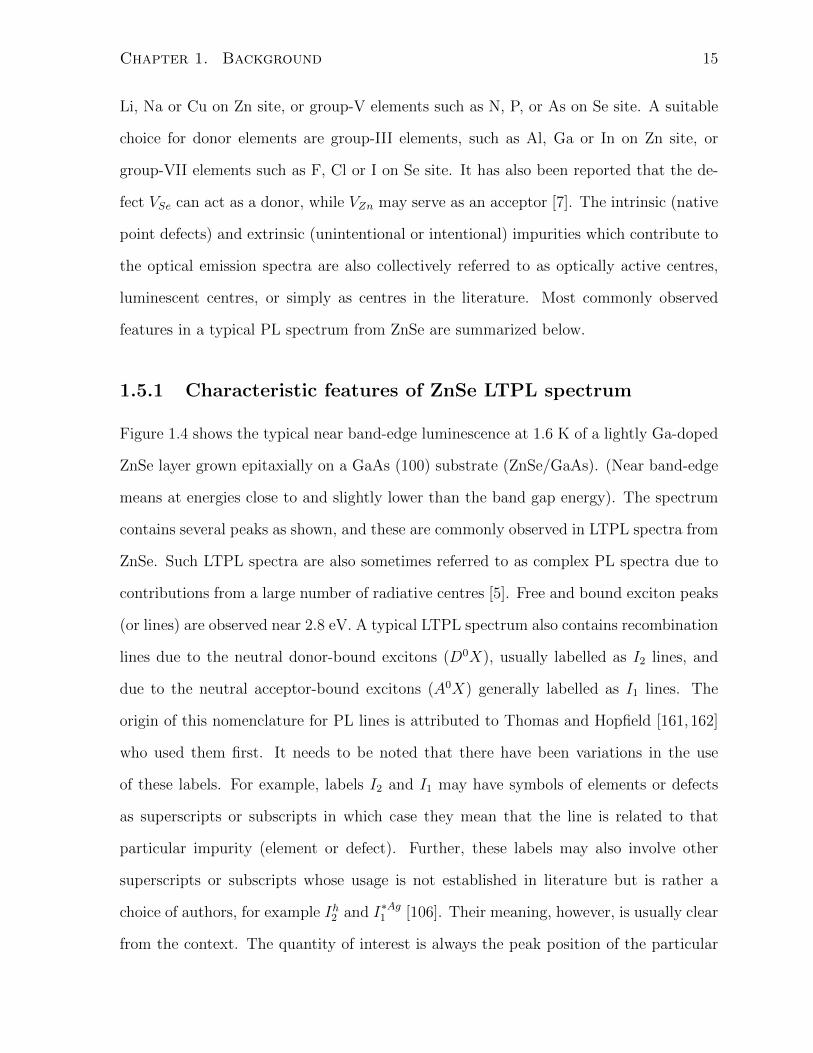
Chapter 1. Background 15
Li, Na or Cu on Zn site, or group-V elements such as N, P, or As on Se site. A suitable
choice for donor elements are group-III elements, such as Al, Ga or In on Zn site, or
group-VII elements such as F, Cl or I on Se site. It has also been reported that the de-
fect VSe can act as a donor, while VZn may serve as an acceptor [7]. The intrinsic (native
point defects) and extrinsic (unintentional or intentional) impurities which contribute to
the optical emission spectra are also collectively referred to as optically active centres,
luminescent centres, or simply as centres in the literature. Most commonly observed
features in a typical PL spectrum from ZnSe are summarized below.
1.5.1 Characteristic features of ZnSe LTPL spectrum
Figure 1.4 shows the typical near band-edge luminescence at 1.6 K of a lightly Ga-doped
ZnSe layer grown epitaxially on a GaAs (100) substrate (ZnSe/GaAs). (Near band-edge
means at energies close to and slightly lower than the band gap energy). The spectrum
contains several peaks as shown, and these are commonly observed in LTPL spectra from
ZnSe. Such LTPL spectra are also sometimes referred to as complex PL spectra due to
contributions from a large number of radiative centres [5]. Free and bound exciton peaks
(or lines) are observed near 2.8 eV. A typical LTPL spectrum also contains recombination
lines due to the neutral donor-bound excitons (D0X), usually labelled as I2 lines, and
due to the neutral acceptor-bound excitons (A0X) generally labelled as I1 lines. The
origin of this nomenclature for PL lines is attributed to Thomas and Hopfield [161, 162]
who used them first. It needs to be noted that there have been variations in the use
of these labels. For example, labels I2 and I1 may have symbols of elements or defects
as superscripts or subscripts in which case they mean that the line is related to that
particular impurity (element or defect). Further, these labels may also involve other
superscripts or subscripts whose usage is not established in literature but is rather a
choice of authors, for example Ih2 and I∗Ag1 [106]. Their meaning, however, is usually clear
from the context. The quantity of interest is always the peak position of the particular

Chapter 1. Background 16
Figure 1.4: Near band-edge luminescence at 1.6 K from Ga-doped ZnSe layer grown
epitaxially on GaAs (100) substrate. General features of the spectrum are explained in
the text. Reprinted with permission from Ref. [7] © 1990 John Wiley & Sons.
peak. The binding energies of common (D0X) and (A0X) usually lie between 2 and 20
meV, and majority of bound-exciton lines can be found in a small energy range below
the free-exciton line. At the lower energy side of the spectrum, lines due to different
donor-acceptor pair (DAP) emissions can be found, which are usually accompanied by
their LO-phonon replicas (i.e., DA-LO, DA-2LO shown in Figure 1.4). Different DAP
emissions in ZnSe are also sometimes labelled Q, P and R, although the use of these
labels is not prevalent anymore.
Bound-exciton and DAP luminescence lines occur due to recombination in the pres-
ence of shallow impurities, and in most cases can be related to a certain point defect
or dopant in the material. Shallow impurities refer to impurities that require an energy
of the order of the thermal energy to cause their ionization. The emission lines in the
PL spectrum which are observed at even lower energies are generally called deep-level
(DL) emission(s). DL emissions are mostly related to the non-optimum growth or doping

Chapter 1. Background 17
conditions which give rise to undesirable defects or impurity-defect levels. DL emissions
in ZnSe can be further distinguished as:
• Y-line emission at 2.605 eV, associated with structural and extended defects [163];
• Lines at 2.5 eV, referred to as S or M lines in the literature. These are often
accompanied by LO-phonon replicas and are correlated with a kind of DAP that
involves shallow donors and distant deep acceptors [163];
• A broad-band emission centred at about 2.3 or 2.4 eV, sometimes also referred to
as “Cu-green” emission. This is normally attributed to unintentional incorporation
of Cu during the growth, and this line is usually accompanied by a specific Ideep1
(or Id1 ) emission line at around 2.78 eV. Ideep1 (or Id1 ) line is considered to be due
to a Cu-acceptor-exciton complex. Ideep1 is also sometimes related to an exciton at
a VZn acceptor centre [164].
• Self-activated (SA) luminescence between 2.14 eV and 1.97 eV, which is related to
VZn vacancies [165] or a VZn/GaZn complex defect centre [7].
1.5.2 Excitonic emission in ZnSe
One of the ways to assess the quality of a semiconductor single crystal is to consider its PL
response. When the PL spectrum is dominated by strong near band-edge features such
as strong and narrow excitonic peaks due to bound excitons and donor-acceptor pairs,
and the intensity of DL emissions is greatly suppressed, this is taken as an indication of
high-purity growth, high crystalline quality, and successful doping (if attempted) without
undesired defects [163, 166, 167]. There have been a large number of reports on PL of
undoped ZnSe crystals and epilayers grown by a variety of methods. The bound exciton
lines observed in the PL spectra of these ZnSe materials have been assigned to different
centres by different authors, and the origin of some of these lines is still questionable.

Chapter 1. Background 18
Doping of ZnSe by different dopant elements has been studied; e.g. Ga [168,169], Cl [170],
Al [171], I [172], and In [173]. By increasing the concentration of a dopant, the donor-
bound exciton line specific to that donor is expected to be enhanced, and the line can be
assigned to that particular dopant. But this assignment is based on the assumption that
the dopant material acts as a donor-like simple substitutional impurity atom. Often,
a more complex donor centre or even an acceptor centre is formed due to the donor
material. This can be observed when the donor-bound exciton line is enhanced, and
other emission lines (especially DL emissions) are affected as well. For example, there
has been a report on rising SA emission for increasing I doping which was explained
by the formation of deep (I − VZn) centres [172]. The binding energies determined for
different donor-bound excitons, and the donor ionization energies in ZnSe films are listed
in Table A.1 [7] in Appendix B.
ZnSe has been doped with N [174], Li [173], P [175] and Na [173] in order to obtain
p-type doping. The most successful method of p-type doping of ZnSe has been the
doping by nitrogen, in particular ZnSe doped by a flux of atomic nitrogen. The difficulty
in obtaining p-type ZnSe is quite often attributed to the self-compensation of acceptor
impurities. A possible explanation of this phenomenon put forward is that Se vacancies
(VSe), which act as donors, are activated as a consequence of the doping process, and
result in a compensation of the acceptor impurities [7]. The binding energies for different
acceptor-bound excitons and the ionization energies for different acceptors in ZnSe films
are listed in Table A.2 [7] in Appendix B. Acceptors introduced in ZnSe can also form
defect complexes, similar to the case of donors and defect complexes of donors. Despite
a large number of reports on doping studies of ZnSe, the values of donor and acceptor
ionization energies and bound-exciton binding energies vary appreciably as shown in
Tables A.1 and A.2, even for ZnSe films grown by the same method. The identification
of donor and acceptor bound exciton lines can be considered to have a wide range of
reports available, but the reports on defect complexes formed by these impurities with

Chapter 1. Background 19
native defects are too few to offer substantial and reliable information on them.
1.6 Optical response of ZnSe nanowires
1.6.1 Distinction from ZnSe single crystals and thin films
The natural questions that arise are, in what ways are the optical properties of ZnSe NWs
(i) similar to and (ii) different from, those of bulk ZnSe and ZnSe epilayers. Dresselhaus et
al. [24] have noted that NWs with diameters larger than a few nm have crystal structure
similar to that of the bulk parent material. This is because the quantum confinement
effects which arise due to confinement of carriers in two-dimensions in NWs do not appear
until the confinement in these dimensions is of the order of the exciton Bohr radius
(aB). aB is the approximate distance between an electron and a hole in an exciton. For
NWs with diameters considerably larger than aB (e.g. d & 10aB) have essentially the
same electronic band-structure as bulk material. A brief introduction to electronic band-
structures is given in Appendix E. Optical transitions in a semiconductor are intimately
connected with their band-structure. The nature of optical transitions in NWs of large
diameters will therefore be similar to those in bulk single crystals. This means that the
peak positions observed in the luminescence spectra of NWs can be directly compared
with corresponding peaks in spectra from their bulk form. It is for this reason that the
PL spectra from NWs of a wide range of materials, particularly those of wide band gap
semiconductors [55,103–109,111–114,119,120], have been explained by comparing them
with the bulk luminescence spectra. The concept of surface excitons (SX) has also been
used to explain PL results in certain cases (e.g. ZnO [176], GaN [177]). Surface excitons
refer to excitons localized at the surface of NWs. In case of ZnSe NWs, there have been
no peaks reported thus far which cannot be explained by assuming bulk-like behaviour.
Chapter 1. Background 20
Distinguishing features
However, there are important differences in optical response of NWs. distinction. The
nature of recombination centres in NWs is quite different due to differences in how these
structures are prepared. In the case of ZnSe, bulk single crystals are grown using high-
temperature melt-grown methods. Even the highest purity source materials used for
their growth contains trace elements (impurities) of varying concentrations (typically
∼1-100 ppm, ppm=parts per million)which are incorporated into the bulk ZnSe crystals
during growth, and are detectable by PL spectroscopy due to its high sensitivity. Crystal
growth of ZnSe from the melt was reviewed by Rudolph et al. [178]. This issue of
residual impurity incorporation is far less significant for low-temperature vapour phase
growth of ZnSe NWs. The issues for growth of ZnSe epilayers originate with the lack
of a suitable substrate. GaAs has almost exclusively been used as a substrate to grow
ZnSe epilayers (e.g., by MBE and MOCVD) leading to inter-diffusion of impurities from
the substrate into the films. The key impurity in this case is Ga, a donor in ZnSe [7],
which appears as one of the dominant features in the PL spectra of ZnSe epilayers [7].
Another important issue with ZnSe epilayers on GaAs substrates relates to the biaxial
strain which arises from the lattice mismatch between ZnSe and GaAs (aZnSe=5.6693
A [179] and aGaAs=5.6533 A [179] giving a misfit strain ∼0.25% [178], ∼0.27 % [7]).
Further, the different thermal expansion coefficients for ZnSe (7.0 × 10⁻⁶ K−1 [178])
and GaAs (5.8 × 10⁻⁶ K−1 [178]) also contribute to this strain. This strain leads to a
splitting of the valence band into heavy-hole and light-hole sub-bands, and PL spectra
acquired from ZnSe epilayers contain PL peaks from these two bands. The top of the
valence band in ZB-ZnSe is doubly-degenerate which means the two bands have the same
energy. This degeneracy is lifted by strain and the band is split into heavy-hole and light-
hole bands. These issues are discussed by Gutowski et al. in their review [7] on optical
properties of ZnSe epilayers and films. ZnSe NWs are different from ZnSe epilayers in
that their optical properties are not affected by the issues of Ga incorporation or strain.

Chapter 1. Background 21
An important question that needs to be answered for ZnSe NWs is then, in the absence
of intentional doping and strain, which optical processes dictate their optical properties?
The above discussion was presented to clarify the need for optical characterization of
ZnSe NWs in order to understand the fundamental processes that govern their optical
properties. This information is crucial in order to be able to fabricate optical devices
based on single ZnSe NWs. It is clear that the above arguments are specific to ZnSe only,
and do not necessarily apply to NWs based on other materials.
Confinement effects in nanowires
Another important aspect of semiconductor NWs relates to the effects of quantum con-
finement and dielectric confinement. In a semiconductor NW, the photoexcited carriers
may be two-dimensionally confined, and free to move along the length of the wire. This
results in a overlap between the electron and hole wavefunctions, thereby increasing the
binding energy of the excitons. Hence, the exciton binding energy can be tuned by chang-
ing the size of the NW, but this tuning can only provide exciton binding energies a few
times their bulk value. Another way to realise the same effect is the dielectric confine-
ment effect [180, 181]. The exciton binding energy may be enhanced when the electric
field lines from a hole to an electron, pass through the insulator when a semiconductor
NW is surrounded by an insulator with smaller dielectric constant. Anisotropy in optical
absorption and emission for semiconductor NWs embedded in dielectric have been dis-
cussed recently [182]. The exciton Bohr radius of bulk ZnSe is aB = 3.30 nm [183]. ZnSe
NWs of diameter < aB would be expected to show quantum confinement effects, and this
has been shown in narrow solvent-grown ZnSe NWs [69]. The fabrication of NWs with
size < aB is challenging using the vapour-phase growth technique, but there is a possibil-
ity to realise dielectric confinement effects, as has been shown for ZnS nanorods as large
as 100 nm in diameter, embedded in polycarbonate membrane pores [184]. Since the ex-
citon binding energy of ZnSe is only 21 meV, dielectric enhancement of exciton binding

Chapter 1. Background 22
energy holds the potential and promise for the room-temperature excitonic devices.
1.6.2 Luminescence characterization of ZnSe nanowires
This section summarizes the recent progress in optical characterization of ZnSe NWs.
PL (along with cathodoluminescence (CL)) has been routinely used for the optical char-
acterization of ZnSe NWs. CL is a technique similar to PL where an electron beam is
used for the excitation of luminescence, and is almost exclusively carried out inside an
electron microscope (EM). The discussion on optical characterization of ZnSe NWs can
be divided into three broad categories and corresponding sub-categories as follows:
• Based on characterization method(s): room-temperature PL (or CL) and low-
temperature PL (or CL) characterization
• Based on crystal structure: ZB, WZ, a mixture of NWs of these two crystal struc-
tures, and NWs with a mixture of two crystal structures (bicrystalline).
• Based on morphology: NWs, nanobelts and nanoribbons, and other morphologies
Table B.1 in Appendix B provides a summary of the reported studies on the optical
characterization of ZnSe NWs according within the above categories. The crystal struc-
tures listed in Table B.1 are as reported by the authors. In cases where crystal structure
was not reported, it was determined from other works by the same authors, and in cases
where other studies were not available, crystal structure was taken to be ZB because
ZnSe predominantly crystallizes in the ZB form [5]. Below, room-temperature (RT) opti-
cal characterization is discussed first, followed by a brief description of low-temperature
optical studies on ZnSe NWs. Discussion on the variations in crystal structure and mor-
phologies is embedded within these sections for brevity and clarity. The discussion is
aimed to provide an overview of the studies while no comments are made on the dis-
crepancies and shortcomings in these results, which appear in Chapter 2. ZB crystal
structure and cylindrical morphology (NW) are implied, unless noted otherwise.
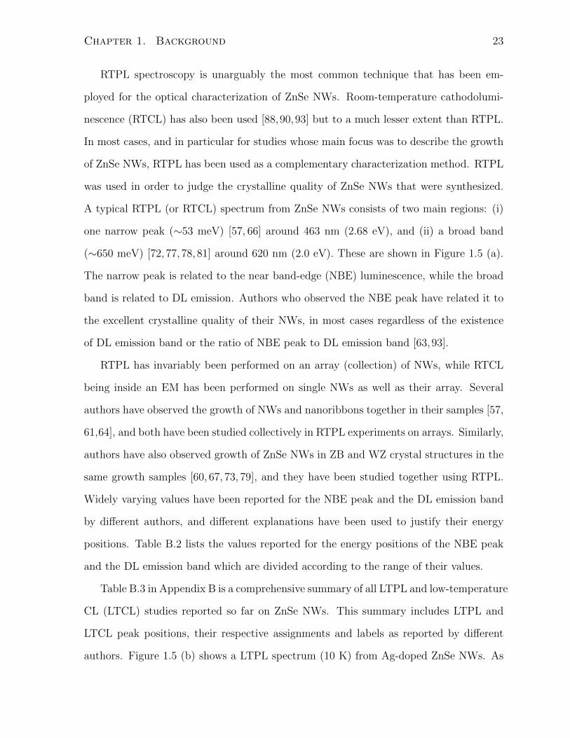
Chapter 1. Background 23
RTPL spectroscopy is unarguably the most common technique that has been em-
ployed for the optical characterization of ZnSe NWs. Room-temperature cathodolumi-
nescence (RTCL) has also been used [88,90,93] but to a much lesser extent than RTPL.
In most cases, and in particular for studies whose main focus was to describe the growth
of ZnSe NWs, RTPL has been used as a complementary characterization method. RTPL
was used in order to judge the crystalline quality of ZnSe NWs that were synthesized.
A typical RTPL (or RTCL) spectrum from ZnSe NWs consists of two main regions: (i)
one narrow peak (∼53 meV) [57, 66] around 463 nm (2.68 eV), and (ii) a broad band
(∼650 meV) [72, 77, 78, 81] around 620 nm (2.0 eV). These are shown in Figure 1.5 (a).
The narrow peak is related to the near band-edge (NBE) luminescence, while the broad
band is related to DL emission. Authors who observed the NBE peak have related it to
the excellent crystalline quality of their NWs, in most cases regardless of the existence
of DL emission band or the ratio of NBE peak to DL emission band [63,93].
RTPL has invariably been performed on an array (collection) of NWs, while RTCL
being inside an EM has been performed on single NWs as well as their array. Several
authors have observed the growth of NWs and nanoribbons together in their samples [57,
61,64], and both have been studied collectively in RTPL experiments on arrays. Similarly,
authors have also observed growth of ZnSe NWs in ZB and WZ crystal structures in the
same growth samples [60, 67, 73, 79], and they have been studied together using RTPL.
Widely varying values have been reported for the NBE peak and the DL emission band
by different authors, and different explanations have been used to justify their energy
positions. Table B.2 lists the values reported for the energy positions of the NBE peak
and the DL emission band which are divided according to the range of their values.
Table B.3 in Appendix B is a comprehensive summary of all LTPL and low-temperature
CL (LTCL) studies reported so far on ZnSe NWs. This summary includes LTPL and
LTCL peak positions, their respective assignments and labels as reported by different
authors. Figure 1.5 (b) shows a LTPL spectrum (10 K) from Ag-doped ZnSe NWs. As

Chapter 1. Background 24
(a) (b)
Figure 1.5: (a) RTCL spectrum from an individual ZnSe NW showing two peaks related
to NBE and DL emission at 2.68 eV and 1.96 eV, respectively. (b) LTPL spectrum (10 K)
from an array of Ag-doped ZnSe NWs. Inset shows the near band-edge region enlarged.
See text for details. Reprinted with permission from (a) Ref. [102] © 2011 Elsevier, and
(b) Ref. [106] © 2011 American Institute of Physics.
was noted earlier LTPL spectra from ZnSe are usually complex due to a large number
of peaks. The LTPL spectrum shown in Figure 1.5 (b) [106] is likely the most complex
PL spectra reported so far on ZnSe NWs. The LTPL peaks were related to the bound
excitons in WZ-ZnSe and to bound excitons related to Ag impurities in ZB-ZnSe. Peaks
due to phonon-replicas and DAP related recombination line due to Ag were also noted.
The LTPL peak positions and their details are listed in Table B.3. Similar to the case of
RTPL, most LTPL studies have been performed on an array of NWs, and LTCL on sin-
gle NWs and their arrays. It has been argued that metal-catalyst diffuses in ZnSe NWs,
and this diffusion influences the optical properties of ZnSe NWs. For example, Xiang et
al. [55] and Jin et al. [76] have related their LTPL spectra from ZnSe NWs to diffusion
of Au, while Liang et al. [120] using Ag and Ga catalysts have claimed that Ag and Ga
act as dopants in ZnSe NWs and that the LTPL peaks from their ZnSe NWs arise due
to Ag and Ga. But these claims are based on little evidence, and not supported by other

Chapter 1. Background 25
studies where Au or other metal-catalysts were used for the growth of ZnSe NWs. It may
also be noted from Table B.3 that there have been no LTPL studies on role of native
point defects in the optical properties of ZnSe NWs. Incidentally, Zhang et al. [103] and
Liu et al. [108] studied ZnSe NWs grown on GaAs substrates, and related LTPL lines
to substitutional point defects (GaZn and AsSe). Similar to the case of RTPL charac-
terization, LTPL characterization has also been performed on mixtures of ZnSe NWs
and nanoribbons [106], mixed NWs of ZB and WZ crystal structures [106, 107, 117] and
bi-crystalline NWs [106, 110, 111, 115, 116]. However, in case of RTPL discrepancies in-
troduced by studying such mixtures are not that significant because RTPL spectra are
much broader and different contributions (e.g. from NWs and nanoribbons) cannot be
easily distinguished. These differences are much more pronounced at low-temperatures,
and cannot be resolved by studying mixtures of NWs. These details are discussed in
Chapter 2.
1.6.3 Influence of heat treatment
One of the methods used to study the role of native point defects on the optical prop-
erties of ZnSe involves modulating the stoichiometry, and studying the resulting optical
response from ZnSe. Stoichiometry refers to the occupancy of Zn and Se lattice sites
in the crystalline material. These procedures may involve, for example: (i) growth of
ZnSe (single crystals, films or NWs) with an extra source of one of the constituent el-
ements (Zn or Se), (ii) heating ZnSe in contact with molten Zn, a process known as
Zn-extraction [185], (iii) post-growth treatment such as annealing in vapours of one of
the constituent elements. These methods are collectively referred to as heat treatment,
because they involve elevated temperatures. There have been studies on the effects of
native defects on optical emission properties, but by far they have been fewer compared
to the extensive work on foreign impurities [7]. Even though a fair number of reports
are available on the effects of native point defects on optical properties of ZnSe, they

Chapter 1. Background 26
are not devoid of controversy. The exact nature of intrinsic defects, and the role they
play in complex low-temperature optical spectra of ZnSe are not completely understood
yet. This can be justifiably attributed to the overlap of PL lines due to some foreign
impurities and the native defects, which makes the unambiguous identification of lines
difficult. The optical properties and quality of ZnSe NWs, similar to those of single
crystals, can be strongly affected by the presence of native defects, arising from the sto-
ichiometric deviations even in high-purity growth conditions. The presence of native
defects adversely affects the optical and electrical properties of ZnSe. For example, na-
tive defects and self-compensation have been implicated in the difficulty in p-doping and
control of conductivity in ZnSe single crystals. It has been established in the literature
that Zni and VSe act as donors [7, 174, 186–188], while Sei and VZn act as acceptors in
ZnSe [7, 174,187,189,190].
(a) (b)
Figure 1.6: RTPL spectrum from ZnSe NWs: (a) grown under Zn-rich conditions showing
stronger NBE emission compared to the weaker DL emission, and (b) grown under Se-
rich conditions showing strong DL emission while NBE emission is absent. Insets show
dominating (a) blue and (b) red luminescence from single ZnSe NWs. Reprinted with
permission from Ref. [72] © 2006 American Institute of Physics.
Philipose et al. [72] have earlier reported on the RTPL experiments on NWs grown
under stoichiometric and non-stoichiometric growth conditions. This growth method
Chapter 1. Background 27
is similar to the one used for the growth of ZnSe NWs studied in this thesis. They
showed that the optical emission characteristics of these NWs can be tuned to obtain
emission in the desired near band-edge (NBE) region or low-energy self-activated (SA)
emission region. This is shown in Figure 1.6(a) and (b), where in (a) the emission
corresponds to the NBE (blue) emission, while in (b) the emission is related to the SA
(red) emission. In particular, they showed using post-growth annealing treatments in Zn
and Se atmospheres, that the near band-edge luminescence can be observed and enhanced
with Zn-treatment, and that this luminescence can be quenched with Se-treatment. They
also showed that this effect is reversible, i.e., the luminescence in either case can be almost
fully recovered following a (Zn-Se-Zn-...) annealing cycle. The reversibility effect that
they observed (in their RTPL measurements) clearly shows that the origin of the near
band-edge and SA-related emissions can be attributed to native defects in the crystal
lattice, and that the concentration of residual impurities in these NWs is very low. This
reversibility effect observed by Philipose et al. [72] on ZnSe NWs is consistent with the
earlier work performed by Roppischer et al. [191, 192] on intrinsic defects in ZB, n-type
ZnSe bulk crystals using LTPL. They observed that the edge emission spectra of ZnSe
undergoes significant change when the crystals were heat treated in Zn or Se atmospheres,
and that this effect was reversible over a few annealing cycles. They assigned a position
0.19 eV above the valance band to the acceptor centre, and associated this to vacancy
of zinc VZn, and a position of 10 meV below the conduction band to the donor centre,
vacancy of Se (VSe) responsible for these effects. In another report by Sekoguchi et
al. [193], they observed a change in intensity of PL lines (Ix = 2.795eV and I2 = 2.797eV )
from hetero-epitaxially grown MOCVD ZnSe layers onto GaAs and Ge substrates after
heat treatment, although they did not assign the centres responsible for the emission.
They also observed appearance of a new line Id1 = 2.780eV after the heat treatment, which
can be associated to the VZn acceptors. The process of using thermal annealing in order to
increase the intensity of luminescence, and in particular enhance blue luminescence, has

Chapter 1. Background 28
been used in the past [186–188,190,194,195], and it has been known that the concentration
of zinc vacancies responsible for the self-activated luminescence can be controlled by
treatment in gaseous or liquid Zn [193–195]. Beyond the work performed by Philipose et
al. [72] using RTPL, there have been no attempts to understand the influence of native
point defects on optical response of ZnSe NWs.
1.7 Summary
An overview of the current state of the art in the field of optical characterization of ZnSe
NWs was given in this chapter. First, a general introduction to II-VI compounds and
ZnSe was presented. This was followed by a summary of recent developments in the
general area of semiconductor NWs, ZnSe NWs and their importance in practical appli-
cations. NTSLs were introduced as an emerging new class of nanomaterials promising
for future nanoscale optoelectronic and photonic devices, and their unique structure was
explained. Thereafter, a general overview of the growth of NWs with emphasis on VLS
growth mechanism was discussed. Optical characterization studies on ZnSe crystals and
epilayers were used to discuss donor and acceptor-bound exciton PL emission in ZnSe.
A typical PL spectrum from ZnSe epilayers was used as an example to highlight the
characteristic features of low-temperature PL spectrum from ZnSe. The distinguishing
features of the luminescence properties of ZnSe NWs were explained in contrast with
the dominating optical processes in ZnSe crystals and epilayers, which do not apply to
NWs. A summary of RTPL and LTPL characterization studies on ZnSe NWs reported
so far in the literature was given with remarks on their general features. The influence
of heat treatment and the role of native point defects in optical properties of ZnSe was
described, and use of heat treatment as a tool to identify native point defects in ZnSe
was also discussed. However, no attempt was made to highlight the gaps in the funda-
mental understanding of optical response of ZnSe NTSLs and NWs. These are discussed

Chapter 1. Background 29
in detail in Chapter 2.
Chapter 2
Motivation and Objectives
2.1 Introduction
A general overview of the progress in optical characterization of ZnSe NWs and the unique
properties of NTSLs were described in Chapter 1. The current chapter outlines the the-
sis motivation and identifies the primary and secondary objectives of this thesis. This
chapter is organized as follows. First, the motivation behind the work is explained based
on the current lack of understanding of the optical and electronic properties of NTSLs.
NTSLs based on ZnSe were chosen as a platform for establishing their fundamental prop-
erties, such as the electronic band gap (Eg,NTSL), using optical spectroscopy as a probe.
It is explained that this cannot be achieved without an unambiguous determination of
the nature of optical transitions in homogeneous (i.e. with no twin-planes) ZnSe NWs
first. Section 2.3 identifies clear deficiencies in the understanding of the fundamental op-
tical properties of homogeneous ZnSe NWs. The importance of the role of native point
defects in the optical response of ZnSe NWs is explained, and a lack of systematic studies
involving native point defects in the literature is highlighted in Section 2.3.1. The opti-
cal characterization of ZnSe NWs using LTPL has invariably been performed on arrays
of NWs. The information obtained from these experiments represents the response of
30
Chapter 2. Motivation and Objectives 31
an ensemble of NWs as opposed to the required knowledge of the optical properties of
single NWs. The limitations and drawbacks associated with the experiments on an array
of NWs are discussed, and the importance of optical characterization of single NWs is
explained in Section 2.3.2 using relevant examples from the literature. Remarks are also
made on the interpretation of existing results on LTPL of ZnSe NWs. It is also empha-
sized that the uncertainties in experimental results can be largely avoided by combining
techniques of optical and structural characterization on the same individual NWs. The
specific primary and secondary objectives of this thesis are outlined in Section 2.4.
2.2 Motivation
NTSLs were introduced in Section 1.3.1 as an emerging new class of electronic materials.
NTSLs have alternating equally spaced homogeneous domains of ZB crystal structure
along the growth direction rotated by 60◦ or odd multiples thereof at a rotation twin-
plane. Their unusual properties and potential in future applications was also discussed
therein. The existence of TSLs was predicted by Ikonic [137] based on the theoretical
calculations of their electronic properties. TSLs did not attract much attention from
researchers initially as an experimental realization of TSLs was not possible at that time.
This changed after the developments in the field of NWs, when experimental synthesis of
NTSLs became a reality. Incidentally, ZnSe was among the first materials on which the
growth of NTSLs was experimentally reported [104]. However, in this work Li et al. [104]
observed a self-organised growth of NTSLs and did not report on any specific conditions
for realization. Since then NTSLs have been synthesised in several materials including
InP [132,196], InAs [124], ZnS [131,135], GaP [196], and SiC [197,198]. There have also
been several reports on the growth of ZnSe NTSLs [77,87,88,96,104,120]. Various models
have been proposed for the growth of NTSLs (e.g. [104, 199, 199, 200]). For example, Li
et al. [104] proposed a model for the occurrence of periodic twins based on the release

Chapter 2. Motivation and Objectives 32
of stored elastic energy resulting from the side-wall facets. In their case, the twin-plane
spacing (d) was linearly proportional to the diameter of NTSLs. However, their model
fails to describe the non-linear dependence observed by other authors (e.g. [124,132]), who
suggested different models for the diameter dependence of the periodicity of twin-planes.
In most of the above reports, the NTSLs were obtained by their natural (spontaneous)
growth with no control over their periodicity. Remarkable progress was demonstrated by
Algra et al. [132] and Caroff et al. [124] where they showed the experimental synthesis
of NTSLs with precise control over their periodicity. Despite this recent progress in the
growth of NTSLs with controlled twin-plane spacings [124,132], the understanding of their
electronic structure and optical properties remains unclear. Because the experimental
evidence is lacking, the role of periodically arranged twin-planes in influencing the optical
and electronic properties of NTSLs has not been understood yet. Some authors are
also of the opinion that the twin-planes in NWs are detrimental to their optoelectronic
performance [201–204], and extensive efforts are being devoted to eliminating twin-planes
in NWs [202,203,205].
A few authors have studied the optical properties of NTSLs using RTPL [77,78,87,88,
96]. Woo et al. [204] found that the RTPL from an array of InP NWs containing rotation
twin-planes at random positions along the length of the NW (i.e. not periodic) showed
weaker luminescence than from those without twin-planes. Philipose et al. [78, 81] have
considered the twin-planes in NWs as structural defects, and related the strong deep-
level (DL) emission they observed from periodically twinned NWs to the presence of
twin-planes. They were however careful in pointing out that the DL emission could also
be a result of the stoichiometric deviations in their samples, and not related to periodic
twinning. Li et al. [104] and Liang et al. [120] have studied the optical properties of
arrays of NTSLs (consisting of NTSLs of different periodicities) using low-temperature
photoluminescence (LTPL) and found that the PL spectrum shows characteristic features
similar to those found in a PL spectrum from ZB-ZnSe. This was explained by comparing

Chapter 2. Motivation and Objectives 33
the PL spectrum from ZnSe NTSLs with that from ZB-ZnSe single crystals and thin films,
as the homogeneous segments in NTSLs are ZB-ZnSe separated by the twin-planes. Li
et al. [104] also observed a weak emission at 2.836 eV (higher than the band gap of
ZB-ZnSe) and related it to the small amount of WZ-ZnSe present in their sample. The
LTPL studies on ZnSe NTSLs performed so far have failed to reveal any information
that connects the periodicity of twin-planes (d) to their optical properties. This is also
true for NTSLs based on other materials [135] which were studied using RTPL. LTPL
characterization has not been reported on NTSLs of other materials.
Attempts have been made to calculate the electronic structure of NTSLs [206, 207],
but were restricted to the diameter dependence of electronic structure of unrealistically
thin NWs; i.e., NWs with diameters ∼1 nm which are very rarely obtained using estab-
lished growth methods. They are also unsuitable for device fabrication using standard
lithographic techniques. For large diameter NTSLs, empirical models fail to predict any
significant change in the electronic structure. In spite of the lack of any experimental and
theoretical evidence, NTSLs have persistently been conjectured to be strong candidates
for band-structure engineering through control over their twin-plane spacing between
successive domains [124,132,133].
As noted previously, the optical characterization of NTSLs based on ZnSe and other
compound semiconductors reported so far has failed to provide any evidence of the role
that twin-plane spacing (d) in NTSLs plays in their optical properties. This lack of
meaningful experimental results on NTSLs can be understood by considering the tech-
nical challenges involved in the nanoscale mapping of the characteristics of individual
NTSLs. This mapping is required to faithfully understand their properties. A discussion
of these challenges is presented in Chapter 3. The information obtained from LTPL on
optical transitions is fundamentally related to the electronic structure of the material.
An unambiguous determination of the origin and nature of the optical transitions in ZnSe
NWs of ZB and WZ crystal structures is a prerequisite before these can be established

Chapter 2. Motivation and Objectives 34
for NTSLs. This is particularly important in view of the current interpretations that
NTSLs are ZB-WZ superlattices or polytypes of the parent material (i.e. intermediate
between ZB and WZ). The origin of the optical transitions in a semiconductor however
is ultimately related to the native point defects. In other words, the recombination lines
mainly arise due to native point defects rather than planar structural defects (except
for the Y-line emission in ZnSe which has been attributed to the structural defects).
Therefore, knowledge of the role of native point defects in ZnSe NWs is required to
fully understand optical transitions in NTSLs. The nature of optical transitions in ZnSe
NWs is unclear yet due to a lack of their extensive LTPL characterization and unclear
interpretation of existing LTPL results.
2.3 Gaps in the understanding of fundamental opti-
cal transitions in ZnSe NWs in literature
A major shortcoming in luminescence studies of ZnSe NWs has been the lack of their
low-temperature optical characterization. As evident from Table B.1 in Appendix B,
the number of reports on ZnSe NWs using RTPL far exceeds those using LTPL for
their optical characterization. Existing reports that describe LTPL from ZnSe NWs are
listed in Table B.1, and their general overview was given in Section 1.6.2. Table B.3 in
Appendix B lists the LTPL peak positions and their respective assignments described
in these studies. In cases where they were reported, the binding energies of donors and
acceptors, and linewidths of emission lines are also listed in Table B.3. Further, any
doping of NWs employed in these works is also indicated. In the following, first the
role of native point defects in the luminescence spectrum from ZnSe NWs is discussed.
This is followed by a discussion on the role of inhomogeneities in as-grown NW samples
that influence the experimentally obtained PL spectrum and render their interpretation
ambiguous.

Chapter 2. Motivation and Objectives 35
2.3.1 Role of native point defects
It was explained in Section 1.6.3 that the optical properties of ZnSe NWs, unlike those
of melt-grown ZnSe single crystals, are not influenced by the presence of unintentional
residual impurities. It was also emphasized that the issues of strain and inter-diffusion
of impurities from the growth substrate are not encountered in the case of ZnSe NWs.
It is therefore important to identify the optical processes and recombination centres that
dictate the optical properties of ZnSe NWs. It is well established in the literature that
deviations from stoichiometry during the growth of ZnSe crystals result in native point
defects [178], which influence their optical and electronic properties [178]. Similarly, the
optical properties of ZnSe NWs can be strongly affected by the presence of native point
defects arising from stoichiometric deviations [72]. In order to precisely identify the
native point defects responsible for their respective PL lines in ZnSe NWs, it is necessary
to carry out a systematic analysis of the LTPL experiments on them, taking into account
the earlier studies that have been reported on annealing and thermal treatment of ZnSe
crystals. Below, it is explained that such systematic studies have not been performed,
and indeed, preliminary studies suffer from incorrect interpretations.
Philipose et al. [72] studied the role of native point defects in optical properties of ZnSe
NWs based on their RTPL experiments and post-growth treatment of ZnSe NWs. They
showed that the PL from ZnSe NWs can be tuned to obtain emission in the near band-
edge (NBE) emission region or the DL emission region by annealing treatments in Zn and
Se vapours, respectively. This is shown in Figure 1.6 and discussed in Section 1.6.3 in
Chapter 1. They related the broad DL emission band to a DAP type recombination where
donors and acceptors were identified as interstitials and vacancies of Zn, respectively. The
experiments described by Philipose et al. [72, 78] using RTPL are significant in showing
that the native point defects play an important role in the optical response of ZnSe NWs.
Besides these works by Philipose et al. [72,78], the native point defects in ZnSe NWs have
not been studied using their LTPL characterization. This is also evident from Table B.3

Chapter 2. Motivation and Objectives 36
where it can be noticed that authors have not related the LTPL peaks to the native point
defects in ZnSe. This can be ascribed to two reasons.
In many cases, the LTPL spectra reported are not the typical complex PL spectra [55,
108,117,118], which are expected from ZnSe. In these cases, the spectra show a few peaks
in the NBE region (actually at energies lower than what is considered NBE region) and
broad DL emission band. In several cases excitonic peaks were not even observed at low-
temperatures [55, 110, 111, 113, 116–118]. This can either be due to the poor crystalline
quality of NW samples, or due to inadequate experimental arrangement used for their
LTPL characterization. In Chapter 3 it is explained that the implementation of PL is
simple for arrays of NWs, but needs to be performed carefully so that the PL signal can
be collected with a reasonable collection efficiency. In cases where the sample quality is
poor and the experimental arrangement is of low collection efficiency, it is not surprising
that the LTPL spectra may not resemble the typical complex PL spectra.
In a few cases, the LTPL spectra from undoped ZnSe NWs are similar to the complex
LTPL spectra from ZnSe single crystals and thin films. But in most of these works,
the LTPL peaks have been related to extrinsic impurities, and justified based on various
reasons. These include, for example, (i) presence of GaZn and AsSe due to the use of
GaAs substrates [103, 108] (DAP peaks), (ii) presence of Al due to the use of alumina
substrate [104], (iii) residual impurities [111], and (iv) Na and Cu from residual impuri-
ties [113]. In other reports on undoped ZnSe NWs, the LTPL peaks have been assigned
to bound excitons, but no attempts were made to identify the impurities responsible
for binding these excitons [103, 104, 107, 109, 110, 115–117]. These facts can also be no-
ticed from Table B.3 in Appendix B. In another example, Ohno et al. [105] regarded the
emission peak at 2.795 eV as due to the excitons bound to VZn. This is an incorrect
assignment because the LTPL peak near 2.795 eV is due to the excitons bound to VSe,
as can also be noticed from Table A.1 in Appendix B. This is despite the fact that the
reference that Ohno et al. [105] have used [208] also regards this peak as due to VSe.

Chapter 2. Motivation and Objectives 37
It is important to emphasize that the growth of ZnSe NWs (or NWs of any material
in general) usually does not result in identical NWs on the growth substrate. In other
words, the NWs can have different concentrations of native point defects depending on
their location on the substrate, and more importantly if the flow of constituent vapours
is affected by other NWs growing in their vicinity. This issue of inhomogeneities on
the growth sample is quite serious which necessitates that optical characterization be
performed on individual NWs. In the next section, the importance of optical studies on
single NWs is explained.
2.3.2 Lack of luminescence studies on single ZnSe nanowires
Most experimental work on LTPL from ZnSe NWs has been on arrays of NWs. There are
only a few reports describing LTPL [110, 111, 115, 116] and LTCL [108, 116] from single
ZnSe NWs. It is important to note that a majority of these reports [110, 111, 115, 116]
originate from the same authors and their main focus was to study the optical properties
of CdSe quantum dots inside ZnSe NWs). These works on single NWs have not revealed
any new information on ZnSe NWs which was not already available from reports on
arrays of NWs. In fact, a few LTPL studies [103, 104, 106, 107, 109] on arrays have
reported more detailed spectra than those on single ZnSe NWs. The low-temperature
optical characterization at the scale of single NWs is important for the following reasons:
1. Area-dependent inhomogeneities on the growth sample: As grown NW sam-
ples are inhomogeneous in that the density of NWs is not uniform on the sample. Also,
the NWs in different regions of the as grown sample may contain native point defects of
different types, and of varying concentrations. For example, Tribu et al. [110] have men-
tioned that in their ZnSe NW samples grown by MBE, many NWs showed practically no
LTPL emission while the others showed strong LTPL. Philipose et al. [77] also noted that
in their ZnSe NWs grown by the vapour-phase transport growth method, different PL
intensities in different areas of the sample. Liu et al. [108] also found variations in LTCL

Chapter 2. Motivation and Objectives 38
from different NWs. In order to determine the intrinsic properties of NWs, it is therefore
important to perform the LTPL experiments on single NWs so that such inhomogeneities
do not influence the results.
2. Ensemble broadening of PL lines: Since the PL signal is collected from a large
number of NWs when studying an array, the LTPL lines appear broader than they really
are; i.e., their measured linewidths (taken to be the full-width at half-maximum, FWHM)
are rather large. This broadening can be termed inhomogeneous broadening, in contrast
to the homogeneous broadening which results from the natural broadening of PL lines.
The importance of the narrow linewidths in terms of homogeneous and inhomogeneous
broadening is explained in Section 3.9.3. Briefly, in general, narrow linewidths indicate
better crystalline and optical quality of semiconductors whereas broadening in PL peaks
is related to disorder in the material which limits optical performance. PL linewidths are
large for an array because different NWs contributing to the PL have different diameters.
In many cases, NWs and nanoribbons exist together in the sample [57, 61, 64, 81, 84, 88,
90, 106, 209], and variations in morphology also add to this inhomogeneous broadening.
In other words, when studying an array of NWs, the optical response of the ensemble
is obtained, while the interest is mainly in intrinsic properties of individual NWs. This
inhomogeneous broadening can be excluded only by studying single NWs. For example,
Wishmeier et al. [210] compared the linewidths of LTPL from an ensemble and from
single ZnO NWs (for many NWs), and found that the linewidths from single NWs are
0.3-0.5 meV smaller than those from an ensemble of NWs. In one particular case, they
found the linewidth for excitonic emission of 1.9 meV for single NWs, and 2.1 meV for
an ensemble of NWs (comprised of about 100 NWs). They related this larger linewidth
in the ensemble to inhomogeneous broadening, relating to the variations in diameters,
morphology and crystalline quality of the NWs in the ensemble. They also confirmed
these variations in different NWs by using SEM imaging. Further, they also found that
the luminescence spectra from single and ensemble ZnO NWs are quite comparable (e.g.

Chapter 2. Motivation and Objectives 39
in terms of peak positions) except for the difference in their linewidths. The narrowest
linewidth of excitonic PL lines reported on NWs is 300 µeV for a single GaN NW by
Brandt et al. [177]. The variation in PL from different NWs was also observed by Brandt
et al. [177]. They found that most individual NWs show different PL spectra, with many
individual NWs exhibiting linewidths larger than 20 meV. In most work on single NWs
or their arrays, the reported linewidths of excitonic PL lines are larger than in their bulk
form. Brandt et al. [177] have also noted that this fact has been largely ignored in the
literature. The narrowest linewidth reported so far for exciton PL lines in ZnSe NWs is
10 meV, which is almost 10 ten times larger than the narrowest linewidths reported on
NWs of other materials (∼1 meV) [211–216]. In most reports on LTPL from ZnSe NWs,
the linewidths of excitonic lines were not reported. Other reported values of linewidths
include 40 meV by Liu et al. [108] (for a peak at 2.783 eV which they related to the
electron-hole plasma in their NWs), and a large value of 165 meV by Hsiao et al. [118]
which was related to the DAP recombination. It is therefore critical that single ZnSe NWs
be studied in order to reveal the intrinsic linewidths of excitonic emissions in their LTPL
spectrum excluding the effects of ensemble inhomogeneous broadening. It is important to
note that by studying single NWs only the effects of ensemble inhomogeneous broadening
can be eliminated, not necessarily those of other forms of inhomogeneous broadening.
3. Undergrowth on the sample substrate: Another issue with experiments on as-
grown substrates relates to the growth of poly-crystalline crystallites of ZnSe and/or
deposition of other materials (e.g. precipitates of Zn or Se) on the substrate surface,
beneath the NWs. Cooley et al. [114] concluded that the PL response from ZnSe NWs
in their samples originated from the undergrowth of deformed ZnSe NWs on the sam-
ple substrate, rather than from the straight NWs which were of main interest. Shan
et al. [107] have studied the optical response of WZ-ZnSe NWs. In their LTPL spec-
trum, they related only two peaks (at 2.841 eV and 2.746 eV) to the WZ-ZnSe, while
the other five peaks were related to the underlying ZB-ZnSe crystallites on the growth

Chapter 2. Motivation and Objectives 40
substrate. Aichele et al. [115] have also assigned one of the peaks in their LTPL spec-
tra from ZnSe NWs to bulk ZnSe that they suggested formed simultaneously with the
growth of ZnSe NWs on the sample floor. Ohno et al. [105] studied ZnSe NWs grown
on a buffer layer of ZnSe using LTPL spectroscopy. They explained their results on
the temperature dependence of PL by taking into account the volume fraction of ZnSe
NWs, R = Vnw/(Vnw + Vepi), where Vnw and Vepi are the total volume excited by the
laser beam of the NWs and the epilayer, respectively. Further, Liu et al. [108] have also
observed that the ZnSe layer underneath the NWs also emits light, and contributes to
the LTCL signal even if by a small amount. These examples clearly illustrate that the
optical properties of ZnSe NWs can not be completely understood when they are stud-
ied using LTPL experiments on as grown arrays of NWs. It is important that NWs be
isolated from the growth substrate and studied individually to exclude the effects of the
underlying material on the growth substrate.
4. Mixture of nanowires and nanoribbons: In many cases of LTPL experiments
on arrays of ZnSe NWs, the NWs were studied together with the ZnSe nanoribbons
(e.g. [106]). Apart from contributing to the broadening of PL lines, as explained above,
these variations in morphologies of nanostructures may also result in variations in PL
spectrum (e.g. different peak positions). For example, Zhang et al. [103] observed a peak
at energy position higher than the band gap of ZB ZnSe in their LTPL work on ensemble
ZnSe nanoribbons. It was in this work that a 10 meV linewidth of an excitonic line was
reported as noted above. In their work on Ag-doped ZnSe NWs, Zhang et al. [106] have
related one peak (at energy position higher than the band gap of ZB ZnSe) to regions
of WZ crystal structure in bi-crystalline (i.e. consisting of both ZB and WZ regions)
nanoribbons. They suggested the existence of ZnSe nanoribbons in their samples along
with that of ZnSe NWs. It is therefore important to study the optical properties of ZnSe
NWs separately from those of ZnSe nanoribbons.

Chapter 2. Motivation and Objectives 41
5. Mixture of nanowires of different crystal structures: Several authors have
observed the existence of NWs in two crystal structures in the same sample [104,107,110,
111,115–117]. Luminescence spectra from arrays of NWs from these samples would clearly
include contributions from NWs with different crystal structures. This would lead to
uncertainties in interpretation of experimental results. A few examples are worth noting
in this regard. Liu et al. [109] have reported the crystal structure of their ZnSe nanobelts
as WZ, but they have related all peaks (seven in the NBE region) to the ZB-ZnSe. In
a similar example, Li et al. [119] reported WZ crystal structure for their ZnSe NWs
but assigned all LTPL peaks to ZB structured ZnSe. The latter two examples point to
inconsistencies in the explanation of LTPL results on ZnSe NWs. Further, there have been
several other reports where authors have studied mixtures of NWs of ZB and WZ crystal
structures [104,115,117]. In other works on LTPL from single ZnSe NWs [110,111,116],
the NWs themselves consisted of regions of different crystal structures. It is clear from the
above, that studying a mixture of NWs of two crystal structures or NWs of mixed crystal
structures, fails to provide information on optical transitions in ZnSe NWs in either
crystal structure. More specifically, the identification of PL lines and their assignments in
such cases remain ambiguous. These uncertainties can be avoided by optically studying
single NWs along with the determination of their crystal structure. It also becomes
apparent from the above discussion that the crystal structure determination of the same
individual NWs which are studied optically can be used to understand the origin of
radiative transitions in relation to the electronic structure.
Based on the above discussion it is evident that the optical response from an array
of NWs is highly convoluted because of several factors. It is also important to note that
more than one of these factors contribute simultaneously to the PL spectrum of ZnSe
NWs and result in broadening of PL lines and uncertainties in results. This explains the
need for optical characterization and associated structural characterization of individual
ZnSe NWs.
Chapter 2. Motivation and Objectives 42
2.4 Objectives
In view of the discussion in this chapter so far, it is evident that:
• NTSLs have emerged as new materials with potential for materials engineering at the
nanoscale. However, an understanding of their fundamental optical and electronic prop-
erties is lacking. This can be attributed to the technical challenges in their experimental
characterization at the scale of single NTSLs.
• In the case of ZnSe, efforts to understand the fundamental optical transitions in LTPL
spectra from NTSLs require prior knowledge of these transitions in homogeneous (i.e.
defect-free) ZnSe NWs in ZB and WZ crystal structures. These are also lacking in the
literature. This can be ascribed to the experimental work on PL from ZnSe NWs being
on a mixture of NWs of both crystal structures. The existing reports which have optically
studied arrays of NWs, suffer from ambiguities in their interpretation.
• The optical transitions in ZnSe NWs are ultimately related to the native point defects,
which have not yet been identified in the literature.
The primary and the secondary objectives of this thesis are as follows:
1. Primary objectives: To determine
(a) The relationship between the electronic band gap (Eg,NTSL) and twin period-
icity (d) of NTSLs: Eg,NTSL = Eg,NTSL(d). The relationship between Eg,ZB,
Eg,WZ , and Eg,NTSL is expected to emerge from Eg,NTSL(d).
(b) The optical performance of NTSLs based on luminescence linewidths (), and
luminescence lifetime τ
2. Secondary objectives: To unambiguously identify
(a) The optical transitions in single ZB ZnSe and WZ ZnSe NWs with determina-
tion of exciton binding energy for donors (EBX (D0X)) and acceptors (EBX

Chapter 2. Motivation and Objectives 43
(A0X)), ionization energies for donors (ED) and acceptors (EA), and ioniza-
tion energies for donors (ED) and acceptors (EA) in a donor-acceptor pair
related transitions.
(b) Physical properties of single ZB-ZnSe and WZ-ZnSe from LTPL spectra, in-
cluding temperature dependence of the electronic band gap (dEg
dT) and strength
of exciton-phonon interactions.
(c) Native point defects responsible for the optical emission in ZnSe NWs, with
determination of EBX (for D0X and A0X), ED and EA for bound exciton
emissions, and ED and EA for DAP-related emissions.

Chapter 3
Experimental Methodology
3.1 Introduction
The work described in this thesis is principally experimental in nature, and existing the-
oretical models were used for the interpretation and analysis of experimental results to
understand fundamental optical properties of ZnSe NWs and NTSLs. The results pre-
sented in Chapter 7 on ZnSe NTSLs however, besides being experimentally novel, pro-
vide new fundamental insights which can not be understood based on existing theoretical
frameworks. These results are supported by the electronic structure calculations which
are briefly described in Appendix E.2. This chapter explains, in detail, the methodology
used for performing the experimental work described in this thesis, while the theoretical
models are presented in Appendix C.2. The use of existing theoretical models in the
case of ZnSe NWs is justified because, as explained in Chapter 1 (in Section 1.6.1), the
nature of optical transitions in ZnSe NWs are not expected to be fundamentally different
from those of ZnSe single crystals and epilayers. The difference lies in the luminescent
centres contributing to these transitions being different in NWs. This is also supported
by the fact that these models have been extensively used in the literature for describing
the optical properties of NWs [105, 106, 108, 217]. Three experimental techniques were
44

Chapter 3. Experimental Methodology 45
used for the characterization of ZnSe NWs and NTSLs, namely (i) PL spectroscopy, (ii)
Time-resolved PL (TRPL) spectroscopy, and (iii) TEM (including related techniques of
HR-TEM and SAD). The fundamentals of PL spectroscopy and TRPL spectroscopy are
described in Appendices C and D respectively, while this chapter is mainly concerned
with their experimental procedures (instrumentation). The details on fundamentals and
principles, instrumentation and operation of a TEM can be found in standard text-books
on electron microscopy [218, 219]. PL spectroscopy was used in two different modifi-
cations referred to as: (i) PL spectroscopy (similar to conventional PL spectroscopy),
and (ii) confocal micro-photoluminescence (µ-PL) spectroscopy. Gustafsson et al. [220]
have pointed out that despite being widely used, the definition of µ-PL spectroscopy is
rather vague. In a traditional sense, when a microscope (or a microscope objective) is
used for the excitation of luminescence in the experimental arrangement resulting in an
excitation spot of size ∼1 µm on the sample, the method is referred to as µ-PL spec-
troscopy [220,221]. This is different from (macro-)PL spectroscopy where the excitation
spot sizes can be larger. Commercially available microscopes are commonly utilized in
µ-PL spectroscopy arrangements [220]. In a broader sense, any PL arrangement with a
spatial resolution of the order of ∼1 µm can be termed µ-PL setup [220]. Spatial resolu-
tion here refers to the size of the excited spot or of the area from where the luminescence
is collected. Confocal µ-PL spectroscopy refers to the particular case when a confocal
arrangement of lenses is used in the µ-PL spectroscopy experimental setup [221–223].
This can be achieved either by using a commercially available confocal microscope or
by designing such an arrangement for specific application(s) in the laboratory, both be-
ing almost equally popular. In the present case, the experimental arrangement was
custom-designed, described in greater detail in Section 3.6. It is to be noted that strictly
speaking, TRPL spectroscopy is not a spectroscopic technique in that the result obtained
is neither a spectrum nor is it plotted as a function of wavelength (or equivalent energy).
Regardless, TRPL and TRPL spectroscopy are used interchangeably in the literature to
Chapter 3. Experimental Methodology 46
refer to the same technique. The term ‘low-temperature(s)’ has been used in this thesis
to imply temperatures close to the liquid-helium (He) temperature (4 K), with actual
temperatures noted at appropriate places.
The rationale behind the choice of these three characterization techniques is described
first in this chapter. This is followed by a brief description of the method used for
the growth of ZnSe NWs and NTSLs. Next, the technical challenges involved in the
characterization of the same individual NWs and NTSLs using these three experimental
techniques is explained based on the difference in sample preparation methods for PL
and TEM methods. The details of the experimental arrangement for PL spectroscopy are
presented next, and its limitations in optical characterization at the scale of single NWs
are highlighted. This is followed by the descriptions of the experimental arrangements
for confocal µ-PL spectroscopy and TRPL. The determination of crystal structure of
NWs and periodicity of NTSLs using TEM is also described briefly. Thereafter, different
experimental conditions used for the acquisition of PL spectra are described together
with the remarks on the normalization of PL results. These also include details on fitting
of the PL spectra to different peak functions. It needs to be clarified that these fitting
procedures do not refer to the fitting of PL spectra to theoretical models. Instead, they
refer to fitting of spectra to one or more peak functions to obtain peak positions and
linewidths more accurately.
3.2 Rationale behind the choice of experimental tech-
niques
PL spectroscopy and TRPL are powerful and well-established techniques for characteri-
zation of optical properties of semiconductors, described in more detail in Appendices C
and D, respectively. In brief, PL and TRPL involve excitation of a semiconductor ma-
terial by light whose photon energy is equal to or greater than the band gap Eg of the

Chapter 3. Experimental Methodology 47
semiconductor. These photons are absorbed in the material and generate electron-hole
pairs. These electron-hole pairs then radiatively recombine emitting photons of energy
corresponding to the optical processes involved in this recombination. In PL, a spectrum
is obtained for intensity of emitted light (actually the collected light, both being pro-
portional to the number of photons emitted) at each wavelength in a certain wavelength
range of interest. These wavelengths can be converted to energy to yield a spectrum
in terms of energy, although in practice the spectra can be presented either in terms of
the wavelength (e.g. [55,111,117]) or energy (e.g. [106,109]) with no loss of information.
See also, for example, Figure 1.5 in Section 1.6.2. The experimental methodology for
PL therefore involves two main steps of excitation and collection (sometimes also called
detection). TRPL differs from PL in that recombination lifetimes are measured which
correspond to the time taken by an electron and a hole to recombine, or equivalently
the time between absorption and recombination. A PL spectrum can also be recorded in
TRPL depending on the instrumentation, and this is quite often the case.
3.2.1 Advantages of PL spectroscopy
PL has been used for the experimental work described in this thesis for three main
reasons:
1. High sensitivity: PL is extremely sensitive to the concentration of native point
defects and impurities in a semiconductor material. In practice, the sensitivity of PL is
limited by the instrumentation used in that not all light emitted by the sample is collected
and only a small fraction of it is measured. This fraction depends on the collection
efficiency of the experimental arrangement, which in turn depends on the accuracy of
the experimental setup, losses (due to reflection and absorption of emitted light) by the
instruments and optical components, and sensitivity of the detector used. It is therefore
important to design experimental setups with maximum achievable collection efficiency.
In general, for carefully designed experimental setups, a sensitivity of 1012–1014 radiative

Chapter 3. Experimental Methodology 48
centres/cm3 can be achieved, corresponding to 10−7–10−9% (considering 1023 atoms/cm3
in a typical semiconductor material). It is worth mentioning that no other semiconductor
characterization technique that can be used on single NWs has sensitivity close to that
of PL, except TRPL which was also used for the experiments.
2. Non-destructive: PL is a non-destructive technique in that there is no damage to
the sample while performing PL, and they can be re-used with other characterization
methods or for further PL experiments. Since in PL a sample is irradiated with light,
photons of light do not cause any damage to the sample. When laser radiation is used
for excitation, it is clear that this is true only for excitation intensities up to a certain
limit. It is not surprising that extremely high laser intensities can even melt the sample,
but such conditions are almost never used in PL experiments. The typical excitation
intensities used are much below the damage threshold of the material. For example,
the damage threshold for ZnSe is 1.2±0.3 GW/cm2 [224] (for laser radiation), while
the excitation intensities typically used are ∼few kW/cm2 (e.g. 0.8 kW/cm2 [106], 5
kW/cm2 [72]), six orders of magnitude smaller. It is crucial for experiments described
in this thesis that optical characterization be non-destructive because single NWs which
were studied optically were also characterized later by TEM and HR-TEM. Also, several
PL experiments were needed to be performed on the same single NW or array samples,
and this was only possible due to the non-destructive nature of PL. Further, no special
methods are required for sample preparation for PL experiments. For study of NWs
attached to a substrate, the substrate can be conveniently used. The situation is however
more complex for experiments involving single NWs, and discussed in detail in Section 3.4.
Note that this is not a limitation of PL, but a demand imposed by the objectives of the
experiments.
3. Contact-less: A significant advantage in using PL is that it is a contact-less method
- i.e., metal contacts are not required for PL experiments. The process of fabricating

Chapter 3. Experimental Methodology 49
metal contacts to NWs is not only tedious, time-consuming and expensive, but would
also render the sample containing NWs unusable for structural characterization using
TEM. This is because the sample containing NWs with metal contacts cannot be easily
used inside a TEM.
Since PL and TRPL are similar in excitation part, and different only in the detection
part, the above advantages also apply equally to TRPL. The advantages mentioned
above are also among the reasons which make these techniques widely used methods for
characterization of semiconductors.
3.2.2 Limitations of PL spectroscopy
PL also has certain limitations as discussed below:
1. Cost: (applicable only to work in this thesis) In general, PL is considered a cost-
effective characterization technique because once the experimental arrangement is made,
the operating costs are minimal especially for room-temperature PL (RTPL) experiments.
However, since all the PL and TRPL experiments described in this thesis were performed
at low-temperatures, a considerable expense was incurred on liquid He required to cool the
sample. Further, the major modification of the experimental setup for PL spectroscopy
to that for confocal µ-PL spectroscopy also involved additional costs.
2. Semi-quantitative: PL is a semi-quantitative characterization technique in that it
is difficult to obtain quantitative information based on a PL spectrum alone. In general,
a large number of measurements are required with a varying parameter, e.g., excitation
intensity, temperature, etc., in order to yield quantitative information. Because PL is
non-destructive, in principle it can be performed an unlimited number of times. The
resulting disadvantage is that more time is required for these additional experiments.
Also, large number of additional low-temperature experiments described in this thesis
also added to the cost (liquid He).
Chapter 3. Experimental Methodology 50
3. Radiative recombination: The information obtained from PL is specific to radiative
recombinations only. Since luminescence light from radiative recombinations is collected
in PL, information on non-radiative recombinations which do not result in light emission
is not contained in a PL spectrum.
The advantages of high sensitivity and PL being a non-destructive and contact-less
method clearly outweigh the disadvantages of extra cost and time. Since TRPL can
be used to obtain information on non-radiative recombinations, combined use of PL
and TRPL provides the required information. TEM, HR-TEM and SAD were used for
structural characterization of ZnSe NWs presented in this thesis because there is no
other structural characterization method that can be applied to single NWs to yield
information on their crystal structure and periodicity of twin-planes in NTSLs. The next
section is a summary of methods used for the growth of ZnSe NWs and NTSLs.
3.3 Growth of ZnSe nanowires and NTSLs
The method used for the growth of ZnSe NWs and NTSLs is based on a Au-catalyzed
vapour-liquid-solid (VLS) growth mechanism. The principles of VLS growth mechanism
were described earlier in Section 1.4. A vapour-phase growth method using a tube furnace
apparatus was used for the growth of NWs and NTSLs on a Si(111) (or Si(100)) substrate.
This is also referred to as chemical vapour deposition CVD method. The methodology
is similar to that described previously by Philipose et al. [72, 81]. The Si substrate was
first cleaned and a thin layer of Au (20-50 nm) was deposited by thermal evaporation.
The source material used was ZnSe powder (Alpha Aesar and SPi Inc., 99.999% purity).
The growth was carried out at a fixed substrate temperature under a constant flow of
Ar carrier gas. No intentional doping was carried out. The growth of ZnSe NWs in
conditions of excess Zn (Se) was carried out with an extra source of Zn (Se) with the
source material.

Chapter 3. Experimental Methodology 51
Philipose et al. [78] and Wang et al. [77] have earlier reported that at growth tem-
peratures higher than 650 ◦C, the NWs obtained contain periodic twinning (i.e. NTSLs).
For the growth of NTSLs, substrate temperatures in the range of 650 ◦-750 ◦C were used.
Apart from the technical challenges involved in the characterization of single NTSLs (de-
scribed in the next section), another difficulty stems from the lack of control over the
twin-plane spacing during their growth using this method. This means that NTSLs with
desired periodicities were not obtained on the growth substrate. This is because the
minor fluctuations in source and substrate temperatures and the flux of vapours in the
vapour-phase growth method (tube-furnace based) result in growth of mixture of NWs.
This mixture contains homogeneous NWs, NTSLs with different twin-plane spacings and
randomly twinned NWs (RTNWs). (A RTNW contains rotation twin-planes at random
positions along its length, in contrast to those in NTSLs which are periodic). In other
words, there was no control over the twin-plane spacings during the growth of NTSLs by
the method used, and NTSLs with varying twin-plane spacings were self-organized on the
growth substrate. This lack of control was compensated by performing a sequence of com-
bined optical and structural characterization experiments on several individual NTSLs,
and NTSLs with a range of twin-plane spacings were then selected. The next section
explains the obstacles that needed to be overcome before this combined characterization
could be performed.
3.4 Obstacles in combined optical and structural char-
acterization of the same individual nanowire
In view of the objectives outlined in Chapter 2, a successful correlation between optical
properties and twin-plane spacing (d) is required in order to establish their correspon-
dence. This, in turn, requires the structural characterization on individual NTSLs to
determine their periodicity (d), and optical characterization on the same NTSL to deter-
Chapter 3. Experimental Methodology 52
mine their fundamental properties, such as the electronic band gap Eg. It is crucial that
experiments on NTSLs be performed on individual NTSLs since the determination of
optical response from an ensemble of NTSLs is not of any significance. The importance
of studies on single homogeneous NWs in contrast to those on an array of NWs has
also been discussed at length in Section 2.3.2 in the previous chapter (Chapter 2). The
requirement of optical characterization on single NWs in direct relation with their micro-
structural characteristics was also emphasized therein. Characterization at the scale of
single NTSL and NWs with combined use of two characterization techniques is extremely
difficult. This combination increases the complexity of the experiments, to the extent
that such studies have not been reported on single homogeneous NWs or NTSLs based on
any material. It is equally important to highlight that the challenges in characterization
of single NWs are compounded as the number of characterization techniques to be used
on the ‘same’ NW is increased. Accordingly, there have been fewer studies that describe
both LTPL and TRPL on the same NW (e.g. InP NWs [216]) than those that describe
LTPL alone. Optical and structural characterization on the same NW is far more chal-
lenging and so far, there have only been three recent reports that describe LTPL and
HR-TEM characterization on the same NW [133, 225, 226], and none on NTSLs. It is
of utmost importance to point out that there has been no study reported so far that
describes LTPL, TRPL and HR-TEM characterization on the same NW (homogeneous
and inhomogeneous). Considering that this is true for NWs of all semiconductor materi-
als being researched by an enormously large research community globally, the magnitude
of the challenge can be understood. The details of these challenges and the required
modifications to the experimental methodology are described below. More specifically,
the next section explains why optical and structural characterization using three differ-
ent techniques cannot be performed on the same NW using routine methodology. It is
re-iterated here that in the following discussion optical characterization refers to LTPL
characterization only, and that RTPL does not yield the information of interest.

Chapter 3. Experimental Methodology 53
3.4.1 Bottleneck - incompatible sample preparation methods
for different techniques
The most important hurdle in optical and structural characterization on the same individ-
ual NW is the incompatibility of the sample preparation and sample mounting methods
used for different techniques. Thus, it is extremely important to find a method that allows
optical and structural characterization to be performed on the same NW. The most com-
mon methods of LTPL characterization involve either immersing the sample in liquid He,
which has been a common method in the past [227–229], or mounting the sample on the
cold-finger of an optical microscopy cryostat. In a typical procedure of synthesis of NWs
using the VLS growth mechanism, a substrate of suitable size (with a thin metal film for
catalyst-assisted growth processes) is used inside the growth apparatus. These include,
for example, a tube-furnace for vapour-phase transport method [60, 68], a high-vacuum
chamber for MBE [67, 105] and MOCVD methods [57, 59]. A variety of materials have
been used as substrates (referred hereafter to as as-grown substrates), including but not
limited to, Si(001) [57,59], Si(111) [72,78], sapphire [91,230], quartz [231], GaAs [64,66],
etc. The NWs grow on the surface(s) of the substrates exposed to vapours and are ready
to be used with optical, structural and electrical characterization methods, typically af-
ter a brief inspection with a SEM or an optical microscope (OM). For low-temperature
optical characterization purposes, two methods are most commonly used for mounting
the sample containing NWs to the cryostat. One is to use the as-grown substrate inside
the cryostat [112], the other is to transfer the NWs to another clean bare substrate ei-
ther mechanically [210] or by sonication in a solution [210] (using a suitable alcohol e.g.
methanol [72]) and then putting a drop of the solution on a substrate. Both methods
result in an opaque sample which is then mounted on the cold-finger of a cryostat using
a cryogenic vacuum grease. Other methods to secure the sample to the cryostat can also
be used, but are less common e.g., use of a liquid Indium seal. The use of vacuum grease

Chapter 3. Experimental Methodology 54
is important to make a good thermal contact between the sample and the cold-finger,
otherwise the sample may actually not be at the temperature shown by the temperature
controller used for monitoring the temperature during the experiments. The opaque sam-
ple thus obtained cannot be used inside a TEM chamber because operation of a TEM is
based on a transmitted beam of electrons. The issue is then making this opaque sample
so thin (at least locally near the site of the NW to be studied) that it can be used inside
a TEM.
This issue has commonly been faced in cross-sectional TEM characterization of semi-
conductor devices previously. Szot et al. [232] proposed a new method of sample prepa-
ration for cross-sectional TEM based on the focused ion beam (FIB) machining of semi-
conductor devices to obtain thin foils for TEM characterization. This method has been
widely used since then for preparing samples for TEM characterization out of semicon-
ductor devices [233,234]. In the simplest cases, the sample containing NW(s) of interest
can be used inside a TEM by using a FIB sputtering of the sample substrate, leaving the
NW to be studied intact. However, the use of this method for sample preparation of NW
samples for TEM characterization has been rare. This is because TEM characterization
of NWs dispersed on TEM grids (described in the next paragraph) is straightforward,
and FIB methods are not needed in general for sample preparation. FIB methods have
been used for specimen preparation for samples containing NWs, however it was not in
connection with optical spectroscopy [235]. In reports on optical characterization of sin-
gle NWs, different NWs have been studied through optical spectroscopy and TEM, i.e.
it is not the same NW which is studied by both methods. Further, this method (FIB)
is impractical when combined optical spectroscopy and electron microscopy are to be
performed because (i) it is very expensive given the high cost of FIB instrument, (ii) it is
time-consuming because FIB sputtering would require at least a few hours for each NW,
and (iii) there is a high risk of damage by the FIB procedure to the NW to be studied.
The structural characterization of NWs using a TEM requires an electron transpar-
Chapter 3. Experimental Methodology 55
ent conducting substrate thin enough for transmission of electrons or a substrate which
allows the NWs to be exposed through holes. This is almost exclusively carried out using
commercially available TEM grids of suitable mesh size and made of a compatible mate-
rial, copper being least expensive and thus most commonly used. These TEM grids are
typically 3 (or 3.05) mm in diameter compatible with most commercially available TEM
sample-holders, and 20-50 microns thick. These TEM grids cannot be used inside the
optical cryostat for low-temperature characterization because being so thin they cannot
be mounted on the optical cryostat using vacuum grease, as that would result in their
destruction. Even if they are not destroyed, they cannot be used inside a TEM chamber
because of the contamination by the hydrocarbons in the grease. Room temperature
optical characterization is certainly possible as there is no need for a good thermal con-
tact and this was done earlier by Zapien et al. [236] for single ZnO nanoribbons. In the
present case however, as explained earlier the objective is to perform low-temperature
optical characterization. There are at least three reports of characterization involving PL
and TEM on the same NW, concurrent with the work described in this thesis. These are
on InP NWs [133], heterostructrure GaAs NWs [225] and heterostructure GaAs/GaAsSb
NWs [226]. Bao et al. [133] used a new kind of TEM grid in their work on InP NWs
which uses a silicon substrate with a window covered by thin (20 nm-30 nm) silicon ni-
tride membrane. They also fabricated gold patterns lithographically on these grids for
dissipation of heat generated by the laser beam. There are however a few issues with us-
ing such grids: (i) the thin silicon nitride membrane is very fragile making the transfer of
NWs on the grid difficult. Even if this is achieved, the grid cannot be used several times
given its fragility, (ii) the problem again is that of mounting the Si substrate (grid) on the
optical cryostat, and (iii) designing metal patterns for heat dissipation is time-consuming
and expensive.
To overcome these issues, a sample holder was custom-designed to hold the TEM
grids, and the sample holder was used inside the optical microscopy cryostat for low-

Chapter 3. Experimental Methodology 56
temperature optical characterization. The NWs were mechanically transferred on the
TEM grids (TedPella Inc.) by bringing the as-grown substrate and grids in close contact.
The sample holder had a circular groove of diameter exactly equal to the diameter of the
grid, and a cover-ring was used above the grid to secure it to the sample holder. Different
sample holders were designed for grids of different diameters (e.g. 3 mm and 3.05 mm).
The height of the sample holder was smaller than the distance from the cryostat window
to the cold-finger of the optical cryostat (1 mm). The sample holder and the cover-ring
were made of Cu. Since Cu is a good conductor of heat, no further modifications (metal
patterns etc) were required to ensure efficient heat dissipation. The cover-ring was useful
not only in securing the TEM grid so that it does not fall out of the sample holder while
handling, but also in facilitating a good contact of the grid with the sample holder, which
in turn would ensure a good thermal contact with the cryostat. It was found that on TEM
grids without a reference scheme, keeping track of the same NW during the experiments
is quite difficult. The grids used were reference-finder type (TedPella Inc., 79750), where
reference marks (letters or symbols) can be used as a coordinate system to locate the
same NW during the experiments. In what follows, the experimental methodology which
enabled different characterization techniques to be implemented on the same NWs and
NTSLs is described in detail. The next section describes the details of the experimental
arrangement for PL spectroscopy.
3.5 Photoluminescence (PL) spectroscopy
The experimental arrangement described in this section was used for the LTPL experi-
ments on arrays of ZnSe NWs using the as-grown substrates. A diode-pumped solid state
laser (Coherent Verdi-V8/V10) with output wavelength of 532 nm was used to optically
pump the Ti:Sapphire oscillator (Coherent MIRA-900F). The output power of Verdi-
V8/V10 can be adjusted up to 10 W, while 8 W was routinely used for the experiments.

Chapter 3. Experimental Methodology 57
The output wavelength of Ti:Sapphire oscillator can be tuned from 700 nm to 990 nm
and the output power, which depends on its output wavelength and pump power from
Verdi-V8/V10 among other factors, can be up to 1.75 W. These other factors include, rel-
ative humidity in the oscillator cavity, absorption at certain wavelengths by water, chiller
temperature and cleanliness of the optics inside the system. The output laser radiation
from the Ti:Sapphire oscillator is pulsed with a pulse-width of 200 fs (1 fs=1 × 10⁻¹⁵
sec) and a frequency of 76 MHz. The output from the Ti:Sapphire oscillator is, in turn,
used to pump a commercial second harmonic generator (SHG) (INRAD Model 5-050),
which uses a BBO (beta-barium borate) crystal (Casix). The laser output from SHG has
similar pulse-width and frequency as the input pump laser with correspondingly half the
wavelength.
The fundamental band-gap Eg of ZnSe is 2.68 eV at room-temperature [72, 102],
Eg,ZB=2.822 eV at 4 K for zinc-blende (ZB) ZnSe [155, 237] and Eg,WZ=2.874 eV at 4
K for wurtzite (WZ) ZnSe [238], corresponding to wavelengths of 463 nm, 439.3 nm and
431.4 nm, respectively. The appropriate wavelength for excitation therefore needs to be
shorter than 431 nm for above band gap excitation of ZnSe. A convenient wavelength
for excitation of ZnSe is 400 nm (photon energy, Eph=3.1 eV) which corresponds to the
output wavelength from the Ti:Sapphire oscillator of 800 nm. This is also close to the
wavelength where the output power from the Ti:Sapphire oscillator is maximum (785
nm). Further, the influence of the exciting laser beam in the luminescence spectrum are
avoided at a wavelength of 400 nm.
The laser beam from SHG is directed to the sample using a set of mirrors and lenses. A
schematic of the experimental set-up is shown in Figure 3.1. The NW sample (as-grown
substrate) is placed inside a continuous-flow type liquid He cryostat (Janis Research,
ST-500) and temperatures down to 3 K can be typically reached, provided the relative
humidity is not too high in the atmosphere. (It should be noted that the lowest temper-
atures reached, also called the base temperature, are not always equal, but are close to

Chapter 3. Experimental Methodology 58
Experimental Setup PL spectroscopy
Verd
i Solid
-
Sta
te L
aser
Ti:Sapphire
Coherent MIRA-900F
LS
AC
Second
Harmonic
Generator
Pin Diode
BS1
BS2
BS3
FM1
FM2
M1 M2
M3
M4
M5
M6
M7
M9
M8
M10
Hamamatsu
C-5680
Streak
Camera
Spectra-
Pro
Spectro
meter
Lens
Cryostat
Optical fibre
Figure 3.1: A schematic of the experimental arrangement used for PL spectroscopy.
(M=mirrors, FM=flip-mirrors (mirrors on flip mounts), BS=beam-splitters, LS=laser
spectrometer, AC=auto-correlator)
the liquid He temperature 4±1 K). The temperature is monitored using a temperature
controller (Lakeshore, Model 320) with an accuracy of ±1 K. The temperature controller
is equipped with a heater which can be used to vary the sample temperature during the
experiments. When required, the excitation intensity (Iexc, excitation power per unit
area) of the laser can be adjusted by using a variable neutral density (VND) filter. It is
a customary practice to note the Iexc or the range of Iexc used, similar to the case of tem-
perature (T ), together with the results. The luminescence signal from the NW sample is
collected using a long-working distance objective (Mitutoyo, [M Plan Apo SL 50]), and
guided to the spectrometer using an optical fibre placed close to the microscope objective,

Chapter 3. Experimental Methodology 59
Spectrometer, Triax-320
Liq. He Cryostat
Optical fibre
Microscope objective
Streak camera
Figure 3.2: Photograph of a section of the experimental arrangement for PL spectroscopy.
The optical fibre is placed close to the microscope objective.
as shown in Figure 3.2. (An optical alignment without using the optical fibre can also
be used instead). The numerical aperture NA of the microscope objective is 0.42. The
PL signal is dispersed by a spectrometer (Jobin-Yvon, TRIAX320). The spectrometer
has three diffraction gratings, and the two most commonly used gratings had 1200 and
1800 grooves/mm. The spectrometer resolution is 0.1 nm at 365 nm and 546 nm. When
converted to energy, this corresponds to a resolution of 0.93 meV and 0.42 meV at these
wavelengths, respectively. The dispersed signal is detected by a liquid nitrogen cooled
charge-coupled device (CCD) detector (Jobin-Yvon, CCD3000). It is to be noted that
the resolution is limited not only by the spectrometer, but also by the detector. The ex-
perimental setup includes other accessories and diagnostics for the laser beam, such as a

Chapter 3. Experimental Methodology 60
laser spectrometer (Pulse-scope, Ape-Berlin) for measuring the wavelength, and an auto-
correlator (Auto-Correlator Mini, Ape-Berlin) to measure the pulse-width. The entire
experimental arrangement involves few other equipment (e.g. oscilloscopes, mechanical
pump(s) etc) and optical elements (e.g. VNDs, optical filters, mirrors, lenses etc) for
the purposes of attenuating and steering the laser beam and the PL signal, for example.
Figure 3.2 shows an image of the detection part of this experimental arrangement.
During LTPL experiments on an array of NWs, an area on the sample is selected
where a large number of NWs (also referred to as an ensemble or a bundle of NWs)
are studied collectively after optical excitation. The PL signal from an array of NWs
is more intense than that from a single NW. This is simply because a large number of
NWs contribute to the PL signal in an array, as opposed to the case of a single NW.
The stronger PL signal from an array leads to the acquisition of PL spectra with high
signal-to-noise ratios (SNR), thereby also reducing the inaccuracies in their collection
and interpretation. Further, characterization of single NWs also requires imaging capa-
bilities in the experimental arrangement so that single NWs can be located for the LTPL
experiments. These factors together explain the lack of reports on single ZnSe NWs using
LTPL spectroscopy. This is, however, in contrast to the NWs of other materials which
have been studied extensively using single NWs [177,210,216,239]. (However, in general,
the number of experimental works on arrays of NWs far exceed those on single NWs for
any material).
The experimental setup for PL spectroscopy described above is highly efficient, es-
pecially for experiments on an array of NWs. The results described in Chapter 4 were
obtained using this experimental setup. However, it showed limitations in functionality
regarding experiments on single NWs. This is because the luminescence signal was cou-
pled directly to the optical fibre and imaging of single NWs was not possible, which is an
important requirement for their characterization individually. It is a necessary step to
locate the single NW to be studied on the sample before the actual PL experiment. This
Chapter 3. Experimental Methodology 61
can be done by taking images of the sample before the PL experiment. More importantly,
the PL signal from a single NW is much weaker in intensity (or signal strength) than that
from an array of NWs which contains a high density of NWs. The collection efficiency
of the setup described above was not optimum for characterization at the scale of single
NWs; i.e., the experiments would have suffered from low signal-to-noise ratios (SNR).
TRPL experiments on single NWs were also not possible on this setup. This is because
the luminescence signal could not be used for TRPL detection since the optical fibre car-
rying the signal was coupled directly to the microscope objective at one end and to the
spectrometer at the other end. TRPL in general is more difficult to detect because the
luminescence signal is resolved both spectrally (in wavelength) and temporally (in time).
Further, the detectors used in the TRPL detection scheme employed in this thesis suffer
from poor sensitivity [240]. This refers to the detector used inside the streak camera
which was used for the TRPL experiments. In other words, a PL spectrum can always
be acquired (if permitted by the instrumentation) whenever TRPL can be measured, but
not vice-versa. For example, in their report on PL from single InP NWs, Bao et al. [133]
have noted that they could not measure TRPL because of the weak luminescence signal
from single NWs.
3.6 Confocal Micro-photoluminescence (µ-PL) Spec-
troscopy
The experimental setup required for optical characterization of single NWs is more in-
volved than that needed for an array of NWs. LTPL studies on single NWs have been
reported on NWs of different materials (e.g. InN [239], ZnO [210], GaN [177], and
InP [216]). It was noted in Chapter 2 that there has been almost no progress in optical
characterization of single ZnSe NWs (when compared with the NWs of other semicon-
ductor materials) in that (i) very few LTPL studies have been reported thus far on single

Chapter 3. Experimental Methodology 62
SHG
Spectrometer
Pin-hole
Microscope objective
Optical fibre
Figure 3.3: Photograph of the experimental arrangement for confocal µ-PL spectroscopy.
Inset in the lower right corner shows the confocal part with a pin-hole in the focal plane.
ZnSe NWs [111,116], (ii) there have been no TRPL studies on ZnSe NWs (not even on an
array of NWs). It is because of this, that the references used below in the discussion are
to NWs of other semiconductor materials. It is important to note that the experimental
modifications described hereafter are not exclusive to characterization of ZnSe NWs, but
can be used with comparable performance for single NWs of any semiconductor material
with necessary changes according to the spectral region of interest. The discussion can
therefore now be expanded to include NWs of all semiconductor materials to provide a
broader perspective.
In the experimental arrangement for PL spectroscopy described in the previous section
the optical fibre for collection of PL signal was placed close to the microscope objective.

Chapter 3. Experimental Methodology 63
In the modified confocal µ-PL arrangement, the optical fibre is placed after the confo-
cal assembly. The experimental arrangement designed for confocal µ-PL spectroscopy
is shown in Figure 3.3 and a simple schematic is shown in Figure 3.4. The extent of
modifications is evident by comparing the position of microscope objective and optical
fibre in Figures 3.2 and 3.3. The instruments used for the excitation and collection of
luminescence are similar in both cases, while the major difference lies in the procedure for
mounting the NW sample. The sample (a TEM grid secured inside the sample-holder)
was mounted on the cold-finger of an optical microscopy continuous-flow type cryostat
using a cryogenic vacuum grease. The sample chamber was evacuated using a mechani-
cal pump before the transfer of liquid He starts in pull-mode using the same mechanical
pump. A quartz-tungsten-halogen (QTH) lamp was positioned to illuminate the sample
with white (broadband) light in normal incidence for imaging purposes. The lumines-
cence and reflected white light from the sample was collected in a reflection geometry
using a long working distance microscope objective lens (Mitutoyo, NA=0.42). After the
cool-down process is complete and a temperature around 4 K is reached, the NW of in-
terest is located using imaging with white light. The sample image obtained at the image
plane lacks good contrast. The white light was passed through a polariser to illuminate
the sample, and the back-reflected light was passed through another polariser (an anal-
yser) before being imaged by a CCD camera (Hitachi KP-32N). In this way images with
good contrast were obtained whose brightness can be adjusted by adjusting the crossed
polarisers. One advantage of this method is that anisotropic crystals (e.g. with a WZ
crystal structure) are easily identified as bright objects, but this also results in extinction
of brightness of the isotropic crystals (e.g. with a ZB crystal structure). This is because
anisotropic crystals rotate the polarization of incident light [241] and appear bright. The
light reflected from isotropic crystals with a certain polarization does not pass through
the analyser with orthogonal polarization, thus making them look dark or invisible (ex-
tinction). The analyser is removed during the LTPL experiments after initial imaging so

Chapter 3. Experimental Methodology 64
He
-Ne
Las
er
Halogen lamp (Illumination)
Streak camera
Pin-hole (200 μm)
Linear translation stage
Excitation
Objective
CCD camera
Fibre
Translation stage
To TV
To detector
VND
BS
Sample
Focal plane
Image plane
Z
X Y
Figure 3.4: Schematic of the confocal µ-PL spectroscopy setup. Inset: Area on an as-
grown sample excited by the laser. The laser spot is elliptical due to the oblique incidence
of the exciting laser beam.
as not to attenuate or otherwise influence the PL signal. The laser excitation was used
in an oblique-incidence mode. This results in a large area of the excited spot which is
elliptical in shape (instead of a circular spot obtained with normal incidence), shown in
the lower left corner of Figure 3.4. The area of this spot is approximately 100 µm ×
50 µm, and this area has been used to calculate excitation intensities (from excitation
powers). The large area of the excited spot is advantageous in the case of experiments
presented in this thesis because of the use of a pulsed excitation with high peak powers.
Due to this large area, Iexc remains nominal despite high peak powers of the pulsed laser.
The PL signal can also be imaged at the image plane to obtain a PL image of the

Chapter 3. Experimental Methodology 65
NW being studied. Through this approach the NWs which are efficient emitters can be
chosen and experiments focused on their studies. It is important to select the NWs which
lie in the open or exposed areas of the grid (i.e. not lying on the grid bars) for subsequent
TEM characterization. In experiments described in this thesis, the NWs studied were
almost always in the open areas. Due to the large mesh sizes (of reference-finder grids)
used, resulting in large open areas, NWs attached to the grid bar at one or both ends
were chosen. However, due to the issue of charging by the electron beam inside the TEM,
several NWs in this configuration were rendered unusable.
The PL signal passes through a periscope assembly, and through a confocal arrange-
ment. The periscope assembly was used to compensate for the height. It does not affect
the characteristics or the performance of the experimental setup in any way and should
not be needed in general. A pin-hole is maintained at the focal plane of the confocal
arrangement, and is used to select the region of the NW of interest. The pin-hole and
the confocal assembly are shown in the inset of Figure 3.3. The focal plane and the
image plane are shown in Figure 3.4. The pin-hole was mounted on a three-dimensional
translation stage to allow adjustment in the focal plane, and to select an area of the
NW (or the whole NW) in the other two planes. The use of a pin-hole is one of the
important distinguishing factors from other reports on LTPL of single NWs. In these
works a pin-hole was not used. In terms of the spatial resolution, in the experiments
described in this thesis the resolution is limited by the size of the pin-hole, not the area
of the excited spot which is large. A spatial resolution of 5 µm can be obtained by using
a pin-hole of diameter 200 µm. The spatial resolution can be changed by using pin-holes
of different sizes (e.g. the spatial resolution is 3.75 µm and 2.5 µm with pin-holes of
diameters 150 µm and 100 µm, respectively). However, as the size of the pin-hole is
reduced, the amount of the signal collected is also reduced. In most cases, a pin-hole
with a diameter of 200 µm was used, while the use of other pin-holes was rare. In LTPL
studies reported in literature without the use of a pin-hole, the resolution is limited by
Chapter 3. Experimental Methodology 66
the area of the excited spot (e.g. 1.5 µm (ZnO [210]), 2 µm (InP [213] and GaN [211]),
3 µm (GaN [177] and InP [216])).
3.7 Time-resolved Photoluminescence (TRPL)
A part of the signal (≈ 50%) is sent towards the entrance slit of a second spectrometer
(ACTON PI 300i), passing through another confocal arrangement without a pin-hole,
as shown in the Figure 3.3. The use of a second pin-hole here would require another
CCD camera at the image plane and would also require adjustments in X- and Y-planes
to synchronize the image with that of the first pin-hole, and in the Z-plane to adjust
the position of the pin-hole in the focal plane. The use of a second pin-hole can be
avoided because it does not improve the spatial resolution or the collection efficiency of
the entire setup. This spectrometer also has three diffraction gratings, and a grating
blazed at 500 nm with 600 grooves/mm was used for the experiments. The efficiency
of the grating is maximum at the blaze wavelength. The spectrometer has a manual
vertical slit whose width can be adjusted from 0 to 3 mm using a micrometer knob.
This second spectrometer is coupled to a streak camera (Hamamatsu C-5680), equipped
with a CCD camera at the detection plane. Figure 3.5 shows a simple schematic of time-
resolved detection using a streak camera. The operating principles of a streak camera are
described in more detail in Appendix D. The photons of incoming luminescence signal
are converted to photoelectrons using a photo-cathode, and are swept (dispersed) in time
using a time-varying high-voltage. These electrons are then imaged by a detector (a CCD
camera in this case) to form an image (the streak image), which contains information
about PL lifetimes. The input optics of the streak camera is placed at one of the exit
ports (with no slits) of the spectrometer. Other accessories used in conjunction with the
streak camera are a delay unit (for adjusting the delay time), a pin-diode (to synchronize
the frequency with that of the laser signal), and a chiller (RTE-4). The streak camera

Chapter 3. Experimental Methodology 67
Incident signal
Time varying high voltage
Streak image
Figure 3.5: A simplified schematic of the detection of time-resolved photoluminescence
TRPL using a streak camera.
has a manual adjustable horizontal slit.
The PL signal enters the spectrometer through a aspheric lens with a high numerical
aperture which helps to obtain a diffraction limited spot at the entrance slit of the
spectrometer and that of the streak camera. Since the PL signal goes through a pin-hole
and two orthogonal slits, the signal will not always be at the entrance slit of the streak
camera and needs to be adjusted before entering the spectrometer. No adjustments can be
made after the entrance slit of the spectrometer. The easiest way to obtain this is to use
the aspheric lens (which couples the signal to the spectrometer) on a XYZ-translation lens
mount, or a XY-translation lens mount which is positioned on a translation stage. The
latter assembly was used in the present experiments. The Z-translation of the translation
stage was used to focus the PL signal at the entrance slit of the spectrometer, and it was
left unchanged. This translation in Z-direction is optional, and should not be needed in

Chapter 3. Experimental Methodology 68
general. It was used here because of space constraints on the optical bench. The XY-
translation of the lens mount was used to move the lens in accordance with the movement
of the pin-hole. This was done by monitoring the laser signal in focus mode (signal is not
swept in time) of the streak camera with minimal gain applied. Despite the high-stability
of the Ti:Sapphire laser, the wavelength of excitation can easily fluctuate by ±0.1 nm.
The SHG output wavelength was recorded using the first spectrometer (described in
Section 3.5), and then the X-translation of the lens mount was adjusted to obtain the
image of the laser signal centred at the same wavelength. This also ensures that the
movement of the lens does not affect the accuracy of the peak positions being recorded.
The Y-axis is then adjusted to maximize the intensity of the signal in the vertical (time)
direction. The delay time is adjusted on the program (HPD-TA) (described further in
Appendix F), and then locked to remove problems of jitter as much as possible. It
was observed that jitter is negligible for the time-range of 3 (1500 ps) and 4 (2200 ps),
appreciable for the time-range 2 (800 ps) and very difficult to control for the time-range
1 (150 ps), which is reasonable for instruments not equipped with jitter-correction optics.
The jitter arises due to two factors, (i) the fluctuations in the frequency of the laser, and
(ii) the electronics inside the streak camera.
The methodology for LTPL and TRPL experiments on the same NWs described
above was simultaneous and performed at the same time on two different computers.
This gives an added crucial advantage in removing the ambiguities that may arise from
fluctuations if the experiments were carried out sequentially (or on different days). These
fluctuations can result from fluctuations in the laser power, sample temperature etc and
also uncontrollable factors such as relative humidity in the atmosphere, heating up of the
mechanical pump, detectors etc.

Chapter 3. Experimental Methodology 69
3.8 Transmission Electron Microscopy (TEM)
For the TEM experiments, the TEM grid was simply taken out of the sample holder and
was used inside a TEM using routine procedures. A JEOL-2010F STEM operating at
200 kV and an aberration-corrected Titan-80-300 (FEI) STEM operating at 300 kV were
used for the experiments. HR-TEM characterization was performed on both instruments.
Selected-area electron diffraction (SAD) patterns were acquired on JEOL-2010F. The
TEM micrographs were acquired, processed and analysed using the DigitalMicrograph
program (GATAN) (listed in Appendix F). The program can also be used to acquire power
spectra (fast-Fourier transform, (FFT) pattern) by selecting an area on the micrographs.
The FFT patterns can be used as diffraction patterns for areas which are too small
to be selected for the acquisition of SADs (or when SAD patterns were not available).
TEM is a powerful tool for characterization of microstructure of materials. However,
its use in this thesis was limited to the determination of crystal structure of NWs and
periodicity of twin-planes in NTSLs. Crystal structure can be determined by using the
information on lattice spacings from HR-TEM micrographs. Also, indexed spots in SAD
patterns can be used for the same purpose. The latter method is more deterministic
than the former because different crystal structures may have similar lattice spacings in
different directions. In this thesis, both HR-TEM micrographs and SAD patterns are
presented, the conclusion about the crystal structure was based on the indexed SAD
patterns. The typical method used for indexing of SAD patterns involves measuring the
distances between sets of diffraction spots, and angles between the lines joining these
spots [218,219]. The ratio of these distances and angles are used to determine the crystal
structure. Since the SAD patterns were calibrated in the present case and only two
crystal structures are involved, their indexing was quite straightforward. The distances
between different sets of spots and angles between different directions were measured.
The distances were compared with the information in crystallographic database (Powder
Chapter 3. Experimental Methodology 70
diffraction file, PDF#00-037-1463 for ZB ZnSe and PDF#00-015-0105 for WZ ZnSe),
and orientation of spots was determined.
3.9 Acquisition and analysis of PL results
The above sections describe the experimental methodology in terms of the arrangement
and application of instruments, and specific procedures that allowed collection of the data
(PL spectra and PL lifetimes). But nothing was said about the details of their acquisition
and later analysis. These include parameters that can be adjusted during the acquisition
of data, and procedures used for normalization of PL spectra and curve-fitting to different
peak functions. This section briefly describes these details, and can be sub-divided into
three sections dealing with (i) data acquisition, (ii) spectral correction and normalization
of PL spectra, and (iii) data analysis using curve-fitting. This discussion is important in
understanding why different PL spectra appear differently, and reasoning behind fitting
them to different peak functions.
3.9.1 Data acquisition
The PL signal is eventually detected and measured by a detector. The most commonly
used detectors include photo-diodes, photomultiplier tubes (PMTs) and CCD based de-
tectors. These detectors differ in their sensitivity, spectral response, cost and usable
lifetimes. All PL spectra described in this thesis were collected using a Si based CCD
detector, and the discussion below is specific for such detectors. The principles in gen-
eral apply to all detection systems, it should be clarified that some of these details apply
slightly differently for each of them. The use of the term ‘detection system’ henceforth
includes all instruments and optical components placed after the sample in the experi-
mental arrangements described earlier. The PL signal from a sample of a semiconductor
material ultimately reflects the quality and characteristics of the sample, but for a given

Chapter 3. Experimental Methodology 71
sample there are three factors that can be easily controlled during the acquisition of PL
spectra and may affect their interpretation. These factors determine the amount of signal
collected, which in turn is related to the spectral resolution and accuracy of the data.
These three factors are discussed next. In this discussion, spectral resolution means the
ability of the detection system to distinguish closely spaced PL lines with linewidths
limited only by the sample, not the instrument. Accuracy of the detection system means
that the individual peaks are recognizable with reasonable signal-to-noise ratios (SNR).
This is important because LTPL spectra from II-VI semiconductors in general contain
several peaks resulting from different optical processes, but their intensities (or signal
strengths) can vary depending upon the contribution of each process to the entire PL
signal. While the stronger peaks are easily recognized, in some cases even without any
fitting, due to their high intensities, the weaker ones with small SNR are not always
reliably interpreted. In literature, these indistinct peaks with small SNR are referred to
as shoulders. In general, both high spectral resolution and high peak intensities cannot
be obtained together, as explained below.
For discussion, the LTPL spectra with high spectral resolution can be termed high-
resolution spectra, distinguished from LTPL spectra with large peak intensities for PL
peaks which can be labelled high-throughput spectra. Different conditions are required
in each case and these can be understood in terms of the three factors mentioned above
and described below.
Integration time ti
The easiest parameter to understand of these is the integration time ti, which is simply the
amount of time over which the signal is collected. Large integration times mean collection
of proportionately more signal which helps to increase the SNR in the spectrum. Weak
PL signal, especially from single NWs, can be collected more reliably with high SNR
using larger ti. However, using large ti has a disadvantage that it tends to reduce the
Chapter 3. Experimental Methodology 72
spectral resolution (i.e. leads to broadening of PL lines) because of the effects of spectral
diffusion [242]. Spectral diffusion is a change in the energy position of a recombination
line due to random fluctuations in the environment of the related recombination centre.
These small spectral shifts are related to the fluctuating local electric fields produced by
the movement of charge carriers in the vicinity of the recombination centres. Thus, high-
resolution LTPL spectra are collected with as small ti as possible to obtain narrowest
possible linewidth of the PL peak of interest which should also be clearly resolved. This
also means that the other peaks in the spectrum (especially the weakest ones) might
not be distinctly recorded as they will be merged with the background noise and appear
only as a shoulder. Further, in general, a change in ti enhances or reduces the signal
proportionately. For example, a particular peak in a LTPL spectrum acquired with ti=2
seconds will be almost twice as strong when compared to a similar measurement with
ti=1 second. In practice, ti cannot be made arbitrarily large as that would slow down
the experiments by the same factor.
Slit-width dslit
Slit-width (dslit), which denotes the width of the slit or entrance aperture of the spectrom-
eter, can also be varied during the acquisition of LTPL spectra. The spectral resolution
is inversely related to dslit, i.e. as dslit is decreased the resolution is increased. This is
because narrower dslit results in less divergence of the beam that enters the spectrome-
ter. This in turn reduces the dispersion in wavelengths inside the spectrometer. Larger
dslit allows more signal to be collected but the change in signal strength is not directly
proportional to the change in dslit, unlike the case of ti. In fact, the amount of signal
varies as d2slit. Therefore, high-resolution LTPL spectra are acquired with the smallest
dslit that allows a clear peak to be recorded. Similar to the case of varying ti, not all
peaks in LTPL spectra can be recorded under conditions of high-resolution. In the case
of high-throughput spectra, larger dslit are used and different peaks can be recorded with
Chapter 3. Experimental Methodology 73
good SNR, but the PL lines are broader and appear to be merged when they are closely
spaced. In general, dslit cannot be made too large as it was observed that several PL
peaks are merged into one with very large dslit.
Excitation Intensity Iexc
The third factor that affects the spectral resolution and throughput is excitation intensity
Iexc. It is clear that larger number of electron-hole pairs are generated when Iexc is
increased, which in general correspond to an increase in signal strength. However, as
discussed in Appendix C.2, this change in signal strength is not directly proportional to
the change in Iexc, but depends on the optical processes involved. Even if the change
is not linear, signal strength can be increased by increasing Iexc (at least in the low-
injection regime). But this also results in loss of resolution because processes such as
exciton-exciton, exciton-electron, and electron-electron interactions which result from
higher Iexc tend to broaden the PL lines. These are essentially many-body processes
which require specialized treatment and are outside the scope of this thesis. Thus, high-
resolution spectra are acquired using minimum Iexc which also results in some PL peaks
not being clearly recorded. High-throughput spectra, on the other hand, are recorded
with nominal Iexc resulting in PL peaks appearing with a good SNR along with some
broadening of these lines.
Based on the above discussion it can be concluded that different conditions required
for acquisition of LTPL spectra are: (i) high resolution: smallest ti, dslit and Iexc, and
(ii) high-throughput: large ti, and nominal dslit and Iexc. Further, it can also be inferred
that high-resolution LTPL spectra will contain fewer PL peaks with noisier background,
in contrast to high-throughput LTPL spectra with larger number of recognizable peaks
and larger linewidths. It should also be noted that in the literature the intensities of
PL peaks have no actual units, and they are reported in arbitrary units. This can
be understood by noting that different authors use different instruments in collecting

Chapter 3. Experimental Methodology 74
PL spectra, and different conditions of acquisition. There is no direct correspondence
between the intensity recorded by the detection system and actual photon counts, other
than that they are proportional. This correspondence can be established by correcting
the PL spectra by spectral response of the detection system, but this is almost never
done. This is discussed further in the next section (Section 3.9.2).
In general, all LTPL spectra presented in this thesis were acquired with different
combinations of varying ti, dslit and Iexc. Specifically, each spectra was acquired about six
times on an average, only the ones with highest resolution compatible with good SNR are
presented in this thesis. In a few cases spectra are acquired under both conditions (high-
resolution and high-throughput) and this is noted where these spectra are presented.
This was done to record PL peaks with sample-limited linewidths.
3.9.2 Spectral correction and normalization of PL spectra
Spectral correction
The PL spectra presented in this thesis are as-acquired (or raw) spectra; i.e., they were not
averaged or otherwise modified. This is because the averaging procedure almost always
influences the peak positions and linewidths of PL peaks, even if this influence is marginal.
This issue is more important in the case of high-resolution LTPL spectra. For example, a
commonly used method of averaging (also called smoothing) is adjacent-averaging where
each data-point in the spectrum is replaced by an average of user-defined number of data
points around the original data-point. As this user-defined number of data-points, labeled
averaging width, is increased the SNR is improved but is accompanied by a reduction
in peak intensity and broadening of the linewidth. Moreover, since most PL spectra in
this thesis were later fit to peak functions (Gaussian or Lorentzian), averaging the data
makes the assessment of goodness of fit based on residuals difficult because the averaged
noise may be mixed with the actual signal. Also, the spectra have not been corrected for
Chapter 3. Experimental Methodology 75
instrument response. This is a common practice in PL spectroscopy of semiconductors as
noted earlier. The reason behind this is that, in general, the instrument spectral response
function is not known or it is not easily available to perform the correction procedure.
This can be further understood by taking into account the number of instruments and
optical elements (lenses, mirrors etc) in an experimental arrangement. For example, in
a typical µ-PL spectroscopy arrangement, these would include: inside the spectrometer
(i) diffraction or prism grating(s), (ii) reflecting mirrors (minimum 2, identical), (iii)
collimating mirrors (minimum 2, identical), and outside the spectrometer (iv) CCD (or
other) detector, (v) microscope objective(s), (vi) optical fibre (when used), (vii) all optical
elements such as neutral density filters, optical filters, cryostat windows, mirrors, lenses
etc. In practice, each of them has a certain characteristic response in the wavelength
region of interest (except possibly for VND where neutral in its name is due to a flat
response over a wide spectral range). The instrument response function in such situations
is a convolution of spectral response functions for all elements, many of which are not
accurately known. Therefore, data corrected by instrument response is more error-prone
than without. Datta et al. [243] have criticized this practice and attributed quantitative
discrepancies and irreproducibility of luminescence spectra in the literature to this culture
of not correcting for instrumental spectral response.
Normalization of PL spectra
Since the PL intensity in a LTPL spectrum is in arbitrary units, normalizing the PL
spectrum by any arbitrary factor has no effect on the peak positions and linewidths of
individual PL peaks. Clearly, the integrated PL intensity (IPL) is changed as a result
of any normalization. PL spectra presented in this thesis have been normalized in some
cases for clarity, especially when a comparison between two or more spectra is made.
These normalization procedures are summarized below.
1. Normalization to unity implies the entire spectrum is divided by the highest value of

Chapter 3. Experimental Methodology 76
PL intensity in the spectrum. The strongest peak in the resulting spectrum then has a
peak height of one (in arbitrary units).
2. Normalization to integration time ti means the entire spectrum is divided by ti, re-
sulting in a spectrum corresponding to a collection time of one unit of ti (which in most
cases is one second). This is useful when comparing PL spectra acquired with different ti.
As discussed earlier in Section 3.9.1, the change in PL intensity is directly proportional
to the change in ti, so normalization with ti does not affect the characteristics of the
PL spectrum. It was also mentioned therein that change in PL intensity is not directly
proportional to changes in dslit or Iexc. Therefore, no PL spectrum has been normalized
to either dslit or Iexc.
3. In general for two or more PL spectra: (i) when peak intensities are compared, no nor-
malization has been performed, (ii) when peak positions or peak linewidths are compared,
peak intensities (heights) are adjusted to be equal for all PL spectra.
4. In experiments to study dependence of PL on Iexc, Iexc was varied but care was taken
to keep dslit and temperature T fixed, and ti was varied as needed. In graphs comparing
Iexc-dependent PL spectra, normalization to unity has been used. When these PL spectra
were fit to individual peaks, normalization to ti was used.
5. In temperature-dependent PL experiments T was varied but dslit and Iexc were kept
fixed while ti was adjusted as needed. In graphs comparing temperature-dependent PL
spectra, normalization to ti has been used. Normalization to ti was also used when these
PL spectra were fit to individual peaks. (The fits to Iexc-dependent and T -dependent PL
spectra are not shown because there are enormously large in number. These are typically
never shown, only the obtained parameters of the fits are presented).
Chapter 3. Experimental Methodology 77
3.9.3 Data analysis using curve-fitting
The peak positions in a LTPL spectra can be determined in two ways: (i) by manually
finding the peak positions from the spectrum (e.g., using a graphing program or image-
processing program), and (ii) by fitting the peaks to different peak functions. Both
these methods have been used in the literature. For example, in the case of LTPL from
ZnSe NWs, ther peak positions in most reports were reported without fitting to any
peak functions [55,103,105,106,108,109,111,113,116–120]. Ohno et al. [105] studied the
dependence of linewidth of excitonic emission on temperature but did not mention any
fitting of PL spectra to obtain the linewidths. It should be assumed that they used a
fitting procedure which was not mentioned. When fitting of PL spectra to peak functions
is used, either a Gaussian or a Lorentzian lineshape is used depending on the broadening
mechanism involved. These can be understood as follows.
The lineshape of free and bound excitons is described by a Gaussian or a Lorentzian
lineshape if they are due to inhomogeneous and homogeneous broadening, respectively [244].
A Gaussian lineshape is expected when the linewidth broadening is a result of crystal
imperfections, impurities or strain, called inhomogeneous broadening. In these cases, the
broadening is dominated by the randomly distributed local variations of the associated
electronic states in the sample. The transition energy of these states vary from one point
to another in the sample resulting in observed broadening. Lorentzian lineshape is ex-
pected when the broadening mechanism is homogeneous broadening related to the lifetime
of the associated excited states. Further, in processes where exciton-phonon interactions
are involved, a Gaussian lineshape is obtained for strong exciton-phonon interaction, and
it is Lorentzian for a weak exciton-phonon interaction. This is because in the case of
strong interactions, the lifetime of every individual exciton created by the absorption of
light is reduced by collisions with phonons and result in lifetime broadening (Gaussian).
In the case of weak interactions, the lifetimes are not significantly affected and homoge-
neous broadening dominates (Lorentzian). It should be pointed out that linewidths due
Chapter 3. Experimental Methodology 78
to homogeneous broadening are rarely observed in practise, and this is evident by the
rather large linewidths reported for excitonic emission in NWs. The reported linewidths
of excitonic emissions from NWs ∼1 meV (discussed in Section 2.3.2) are not entirely
due to homogeneous broadening, but also include contributions of inhomogeneous broad-
ening. This is because crystals and crystalline NWs almost always contain impurities
(intrinsic or extrinsic), and often also contain structural imperfections. In general, the
broadening of linewidths includes contributions from both homogeneous and inhomoge-
neous broadening mechanisms, and it is not possible to accurately determine whether
the broadening observed is entirely homogeneous or inhomogeneous. Because of this, in
the use of peak functions to fit the PL spectra, both Gaussian [104, 107, 217, 245–247]
and Lorentzian [148, 231, 248, 249] lineshapes have been used by different authors to fit
excitonic PL lines. The use of a Gaussian lineshape by Brandt et al. [177] to fit an
exciton peak (linewidth <300 µeV) is debatable in that a Lorentizan lineshape may have
been a better choice. This is because a linewidth of <300 µeV is quite likely to be a
result of purely homogeneous broadening. It needs to be emphasized that the use of one
or the other peak function for curve-fitting in the literature does not result in discrep-
ancies. This is because a fitting procedure using peak functions is only used to obtain
peak positions and linewidths more accurately, and the error in such fitting is much less
than the experimental errors. In other words, the error in a particular peak position (or
linewidth) obtained by using different peak functions (Gaussian or Lorentzian) is more
likely to be due to experimental error rather than the use of different functions for fitting.
(It is clear that the choice of peak function is critically important when study is related
to the broadening mechanisms or exciton-phonon interactions).
A choice of appropriate peak function for curve-fitting can be made by using both
functions at first to fit the curves, and then making a choice based on the goodness of fit in
each case. This was done, for example, by Chen at el. [244]. Similarly, for the PL spectra
presented in this thesis, both function were used first (for a few spectra only). It was

Chapter 3. Experimental Methodology 79
found that the fitting method using Lorentizan lineshapes reproduces the experimental
spectra better than that using Gaussian lineshapes. This points to a greater contribution
of homogeneous broadening in the linewidths and weak exciton-phonon interactions. A
Lorentzian lineshape was therefore used to fit PL spectra in the near band-edge NBE
region (excitonic emissions are located in this region). Further, almost all PL spectra
presented in this contain multiple peaks, the number of which is not always obvious. In
the fitting procedure, the multi-peak spectra is first fit to the number of peaks which are
obvious from the PL spectrum. This number is increased gradually until the χ2 error is
minimized. Statistically, minimization of χ2 means finding the values of the fit parameters
such that the sum of the squares of the deviations of the theoretical curve(s) from the
experimental data points for a range of independent variables are minimum. This is a
standard procedure for fitting of multi-peak spectra [250]. The deep-level (DL) emission
appear as broad symmetrical bands, and they are described by a Gaussian lineshape. A
Gaussian lineshape was used for fitting of DL emission band(s) in the PL spectra. It is a
customary practice to note the function used for curve-fitting and the number of peaks
obtained from such a fitting procedure along with the results. This has been followed in
describing the results in this thesis.
3.10 Summary
In this chapter the experimental methodology was described in detail. The entire ex-
perimental procedure consists of two optical characterization techniques namely, LTPL
spectroscopy and TRPL, and one structural characterization technique of TEM (includ-
ing HR-TEM and SAD). First the rationale behind using these three characterization
techniques was described. The advantages and limitations of PL and TRPL methods
were also discussed. This was followed by a brief description of the growth method used
for the synthesis of ZnSe NTSLs and NWs. The technical difficulties involved in a com-
Chapter 3. Experimental Methodology 80
bined use of three characterization techniques on the same individual NTSL and NWs
were described in detail. The lack of any experimental work so far that describes the use
of these three characterization methods on the same NW (independent of the material)
was also emphasized. A new methodology was proposed based on the design of a cost-
effective sample-holder, and implementation of confocal µ-PL spectroscopy and TRPL
techniques on a purpose-built confocal optical microscope setup. The experimental ar-
rangement for PL spectroscopy was described which was used for the characterization
of array of ZnSe NWs. The limitations of this experimental arrangement were also
pointed out. The experimental arrangements designed for confocal µ-PL spectroscopy
and TRPL were described in detail such that the experiments can be reproduced by
others. The structural characterization of ZnSe NTSLs and NWs using TEM was also
briefly discussed. The experimental conditions used in the acquisition of LTPL spectra
were discussed. The variations in signal-to-noise ratios (SNR) in different spectra were
related to integration times (ti), slit-width (dslit) and excitation intensity (Iexc). Nor-
malization procedures used for normalizing the PL spectra were described, while the use
of peak functions in curve-fitting was discussed in relation to the analysis of PL spec-
tra. The experimental methodology described in this chapter may be considered as an
important contribution since it can be utilized to study individual NWs (homogeneous,
heterostructures, NTSLs) of any material by combined luminescence spectroscopy and
electron microscopy. Further, even more characterization techniques (e.g. absorption
and Raman spectroscopy) can also be realized in this experimental arrangement.
All characterization experiments described in this thesis were designed by the author.
All the LTPL and TRPL experiments presented in this thesis were performed by the
author. Structural characterization utilizing TEM and HR-TEM was performed at an
outside facility (Canadian Centre of Electron Microscopy) dedicated for research using
electron microscopy techniques. These were done with the assistance of technical staff at
this facility, the inputs specific to the experiments were those of the author. Exceptions

Chapter 3. Experimental Methodology 81
to the authors’s contributions in experimental work are as follows. The growth of ZnSe
NWs studied in this thesis was performed in collaboration with other researchers at the
author’s facility. The electronic structure calculations of NTSLs, which were helpful
in validating the experimental results were carried out in collaboration at the author’s
facility.
Chapter 4
Influence of stoichiometry on optical
response
4.1 Introduction
It has been discussed in detail in Chapter 1 how deviations from stoichiometry in ZnSe
single crystals and films influence their optical and electronic properties. Details on the
procedures for heat treatment and earlier observations on stoichiometric effects were also
presented therein. In Chapter 2 it was explained that the role of native point defects on
the optical response of ZnSe NWs has not been studied. This chapter presents the results
on the detailed PL characterization and their systematic analysis for ZnSe NWs. PL from
vapor-phase grown undoped ZnSe NWs grown under excess Zn and Se growth conditions
was studied. In particular, the dependence of PL on excitation intensity (Iexc) for ZnSe
NWs grown under the conditions of excess Zn was analyzed. Luminescence spectra are
characterized by strong near band-edge luminescence with negligible deep-level emission.
PL spectrum from ZnSe NWs grown under the conditions of excess Se shows contrasting
features, and is dominated by deep-level emission with negligible emission in the near
band-edge region. Henceforth, the use of term NWs implies ZnSe NWs, unless noted
82

Chapter 4. Influence of stoichiometry on optical response 83
otherwise.
4.2 Results
In this section the results for PL measurements on ZnSe NWs are presented, followed by
their discussion in the following section1.
4.2.1 Low-temperature PL spectra
1 . 6 1 . 8 2 . 0 2 . 2 2 . 4 2 . 6 2 . 8 2 . 3 2 . 4 2 . 5 2 . 6 2 . 7 2 . 8
P L : Z n S e N W s T e m p . = 3 . 1 K I e x c = 5 W / c m 2
( a ) ( b )
E n e r g y ( e V )
PL In
tensity
(arb.
units)
A
E
DC
P L : Z n S e N W s I n d i v i d u a l p e a k s S u m o f i n d i v i d u a l p e a k s
E n e r g y ( e V )
B
Figure 4.1: (a) LTPL spectrum from ZnSe NWs grown under excess Zn growth conditions.
The PL was taken at 3.1 K with average Iexc=5 W/cm2. (b) Near band-edge region of
the spectrum shown in (a), showing three peaks and a shoulder near the lowest energy
peak. These peaks can be resolved into five different emission peaks.
Figure 4.1 (a) shows the LTPL spectrum for excess Zn NWs at liquid He temperature
using average Iexc=5 W/cm2. The LTPL spectrum shows dominant emission in the
1Contents of this chapter partially appear in Ref. [112] (author’s work). Reprinted with permissionfrom Ref. [112] © 2008 American Institute of Physics.
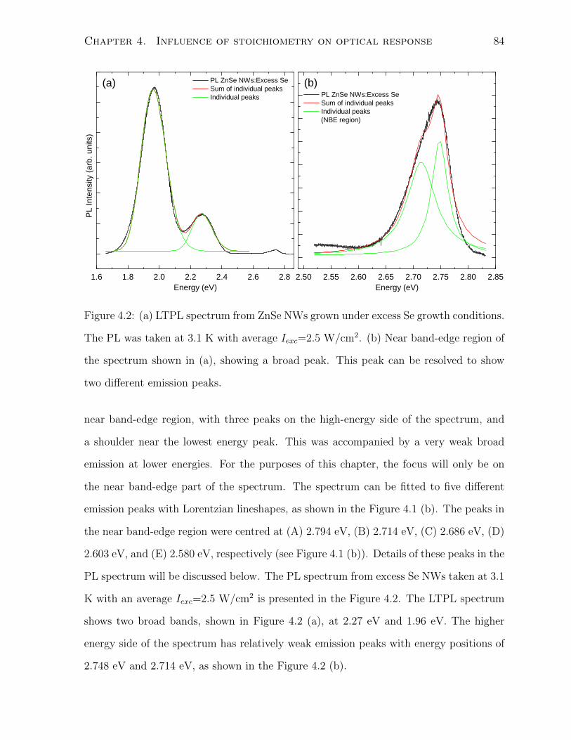
Chapter 4. Influence of stoichiometry on optical response 84
1 . 6 1 . 8 2 . 0 2 . 2 2 . 4 2 . 6 2 . 8
PL In
tensity
(arb.
units)
E n e r g y ( e V )
P L Z n S e N W s : E x c e s s S e S u m o f i n d i v i d u a l p e a k s I n d i v i d u a l p e a k s
( a )
2 . 5 0 2 . 5 5 2 . 6 0 2 . 6 5 2 . 7 0 2 . 7 5 2 . 8 0 2 . 8 5
P L Z n S e N W s : E x c e s s S e S u m o f i n d i v i d u a l p e a k s I n d i v i d u a l p e a k s
( N B E r e g i o n )
( b )
E n e r g y ( e V )
Figure 4.2: (a) LTPL spectrum from ZnSe NWs grown under excess Se growth conditions.
The PL was taken at 3.1 K with average Iexc=2.5 W/cm2. (b) Near band-edge region of
the spectrum shown in (a), showing a broad peak. This peak can be resolved to show
two different emission peaks.
near band-edge region, with three peaks on the high-energy side of the spectrum, and
a shoulder near the lowest energy peak. This was accompanied by a very weak broad
emission at lower energies. For the purposes of this chapter, the focus will only be on
the near band-edge part of the spectrum. The spectrum can be fitted to five different
emission peaks with Lorentzian lineshapes, as shown in the Figure 4.1 (b). The peaks in
the near band-edge region were centred at (A) 2.794 eV, (B) 2.714 eV, (C) 2.686 eV, (D)
2.603 eV, and (E) 2.580 eV, respectively (see Figure 4.1 (b)). Details of these peaks in the
PL spectrum will be discussed below. The PL spectrum from excess Se NWs taken at 3.1
K with an average Iexc=2.5 W/cm2 is presented in the Figure 4.2. The LTPL spectrum
shows two broad bands, shown in Figure 4.2 (a), at 2.27 eV and 1.96 eV. The higher
energy side of the spectrum has relatively weak emission peaks with energy positions of
2.748 eV and 2.714 eV, as shown in the Figure 4.2 (b).

Chapter 4. Influence of stoichiometry on optical response 85
4.2.2 Excitation intensity dependence of PL spectra
The Iexc dependence of the PL spectrum of a semiconductor can be analyzed to yield
detailed information on the radiative recombination mechanisms. In particular, the type
of transition and the ionization energies of donor and acceptor impurities for a donor-
acceptor pair (DAP) transition can be determined. The variation of integrated intensity
of PL emission band with Iexc gives information about the type of radiative transi-
tion [251] (although this information is not exhaustive as will be described below). The
dependence of peak energy of a DAP emission peak on Iexc provides information about
the ionization energies of the involved donor and acceptor levels introduced by impurities
and intrinsic defects.
PL measurements were made at varying Iexc and all spectra for Iexc-dependent PL
were taken at 3.1 K using an excitation wavelength of 391 nm (3.17 eV). The laser
Iexc was varied between 50 mW/cm2 and 25 W/cm2 using a neutral density filter. The
parameters being studied as a function of laser Iexc are integrated PL intensity (IPL)
and peak energy (Ep) for individual emission peaks. Figure 4.3 shows the PL spectra
for different Iexc in the near band-edge region of the spectrum. Some spectra taken at
intermediate values of Iexc have been omitted for clarity. The PL spectra at all Iexc show
three peaks as described above. Each spectrum was fitted to five different emission peaks
and the fit parameters (Ep and IPL) were used for the analysis described below. The
theoretical models used in this analysis are described briefly here, while further details
on them are given in the Appendix C.2.1.
The variation of IPL with laser Iexc can be used to designate the underlying recombina-
tion processes and to evaluate the crystal quality from that information. This evaluation
involves the observation of PL peaks related to bound excitons and DAP-related transi-
tions in the near band-edge region of the LTPL spectrum. Schmidt et al. [251] considered
the different transition mechanisms involved in the recombination processes in a semicon-
ductor material. They analytically solved a set of simultaneous rate equations for these

Chapter 4. Influence of stoichiometry on optical response 86
2 . 3 2 . 4 2 . 5 2 . 6 2 . 7 2 . 8
2 5 W / c m 2
1 0 W / c m 2
5 W / c m 2
0 . 5 W / c m 2
0 . 0 5 W / c m 2
T e m p . = 3 . 1 K
PL In
tensity
(arb.
units)
E n e r g y ( e V )
Figure 4.3: Dependence of PL from ZnSe NWs grown with excess Zn on Iexc. The average
Iexc was varied from 50 mW/cm2 to 25 W/cm2. All spectra were recorded at 3.1 K.
processes with assumptions on the excitation, as well as on radiative and non-radiative
recombinations mechanisms. They showed that the variation of IPL with Iexc can be
expressed by a power law relation:
IPL ∝ Ipexc (4.1)
where p is a coefficient. They ascertained that for free-exciton and bound-exciton emission
the value of p lies between 1 and 2, while p < 1 for free-to-bound and donor-acceptor pair
Chapter 4. Influence of stoichiometry on optical response 87
recombinations. [251]. These values of p can also be understood as follows. Since the
DAP-related transitions are limited by the density of defects, their PL intensity saturates
as Iexc is increased. Since excitons form independently of the defects, their p values are
larger than 1.
Figure 4.4 shows a log(IPL) − log(Iexc) plot for all the peaks shown in Figure 4.1
(b), and for all Iexc used in the experiments (some can be seen in Figure 4.3). Based
on the model described above given by Schmidt et al. [251], p was found to be 1.19 for
emission peak A (2.794 eV), indicating that this is an excitonic emission. Using the
band-gap of ZnSe (Eg = 2.822 at 4 K) [155, 237], and the binding energy of the free
exciton (EFX = 21 meV) [252], the binding (localization) energy of this exciton to the
impurity is found to be EBX = Eg − EFX − Ep = 2.822 − 0.021 − 2.794 = 7 meV. (Ep
refers to the energy position of the peak under consideration). Using the empirical rule
of Halsted and Aven [253], the binding (ionization) energy of the impurity is 35 meV, if
it is a donor, and 70 meV if an acceptor. p values for B (2.714 eV) and C (2.686 eV)
emissions were found to be 0.76 and 0.68, respectively, implying that the recombination
process is either free-to-bound or DAP recombination. It will be seen later that these
are actually DAP-related transitions. The D (2.603 eV) and E (2.580 eV) emission peaks
show a sub-linear dependence on Iexc with p=0.66 and 0.94, respectively.
In LTPL from DAP-related recombinations, and for sufficiently distant donor and
acceptor pairs, the energy of the emitted photon Em is given by [254]:
Em = Eg − (EA + ED)− E(r) (4.2)
where EA and ED are the acceptor and donor ionization energies, E(r) = −e2/εr is the
Coulombic interaction energy of the donor-acceptor pair separated by a distance r, and ε
is the low-frequency dielectric constant. Pair recombination is often comprised of a series
of closely packed lines corresponding to different values of r, and in some cases, like here,
this series of lines results in a broad band. It has been observed that the band maximum
energy (peak energy) shifts to higher energies as the Iexc is increased. For low enough
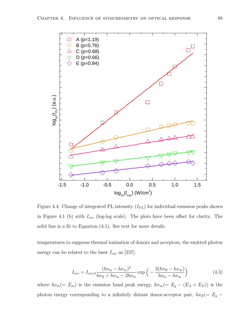
Chapter 4. Influence of stoichiometry on optical response 88
- 1 . 5 - 1 . 0 - 0 . 5 0 . 0 0 . 5 1 . 0 1 . 5l o g 1 0 ( I e x c ) ( W / c m 2 )
log10
(I PL) (a
.u.)
A ( p = 1 . 1 9 ) B ( p = 0 . 7 6 ) C ( p = 0 . 6 8 ) D ( p = 0 . 6 6 ) E ( p = 0 . 9 4 )
Figure 4.4: Change of integrated PL intensity (IPL) for individual emission peaks shown
in Figure 4.1 (b) with Iexc (log-log scale). The plots have been offset for clarity. The
solid line is a fit to Equation (4.1). See text for more details.
temperatures to suppress thermal ionization of donors and acceptors, the emitted photon
energy can be related to the laser Iexc as [237]:
Iexc = Iexc,0(hνm − hν∞)3
hνB + hν∞ − 2hνmexp
(− 2(hνB − hν∞)
hνm − hν∞
)(4.3)
where hνm(= Em) is the emission band peak energy, hν∞(= Eg − (EA + ED)) is the
photon energy corresponding to a infinitely distant donor-acceptor pair, hνB(= Eg −

Chapter 4. Influence of stoichiometry on optical response 89
(EA + ED) + e2/εRB) is the emitted photon energy of a donor-acceptor pair separated
by a shallow impurity Bohr radius (RB), and Iexc,0 is a constant of proportionality. The
values of hν∞, hνB and Iexc,0 are determined using a non-linear least square fit to the
experimental data. As the laser Iexc is increased, closely-lying donor-acceptor pairs are
favoured, and the transition energy moves to higher energy according to Equation (4.2).
This relation assumes that the generation rate of neutral pairs and their annihilation by
recombination rate are equal. Given that pulsed excitation was used in measurements
described in this chapter, an assumption has been made that the relation holds for the
experiments described here. Since the direction of energy shift is opposite to that due to
the temperature dependence of the Eg, this method provides an easy way to identify the
donor-acceptor pairs. Since the peak energy for peaks B (2.714 eV) and C (2.686 eV)
increases with increasing Iexc, these are associated with DAP-related transitions, rather
than to free-to-bound transitions.
Figures 4.5 and 4.6 show the dependence of peak energy on Iexc for peak B (Ep=2.714
eV) and peak C (Ep=2.686 eV), respectively. The solid lines correspond to the Equa-
tion 4.3 above. The peaks B and C shift to higher energy as the Iexc is increased, and
Equation 4.3 can be used to model this behavior. The value of the fitting parameter
Iexc,0 includes a constant of proportionality factor, and hence is irrelevant to the dis-
cussion here. The fit parameters and their detailed analysis are presented in the next
section.
4.3 Discussion
Previously, Roppischer et al. [191, 192] studied the intrinsic defects in ZnSe crystals
following annealing in Zn and Se rich atmospheres. In their earlier work [191], they
reported that after Zn-treatment, a new line I∗2 appears in the PL spectrum, and ascribed
it to the intrinsic donor V xSe (neutral Se vacancy) with a binding energy of 2 meV.

Chapter 4. Influence of stoichiometry on optical response 90
2 . 7 0 6 2 . 7 0 7 2 . 7 0 8 2 . 7 0 9 2 . 7 1 0 2 . 7 1 1 2 . 7 1 2
0
5
1 0
1 5
2 0
2 5I ex
c (W/cm
2 )
P e a k E n e r g y ( e V )
Figure 4.5: Variation of peak energy with Iexc for emission peak B at 2.714 eV (shown
in Figure 4.1 (b)). The solid line is a fit to the Equation 4.3.
The binding energy of the donor was reported to be 10 meV below the bottom of the
conduction band. In their work [191], the samples were excited using the UV-filtered
high-pressure mercury lamp. In their later work [192], where the samples were excited
using the laser radiation, they did not observe this line. Instead, they observed another
line (referred to by them as “D-line”) at 443.8 nm (2.7937 eV), and they related this
to the exciton-donor interaction. Since this line is at a similar energy position as the
A (2.794 eV) line, and based on the other evidence reported below, this 443.8 nm line
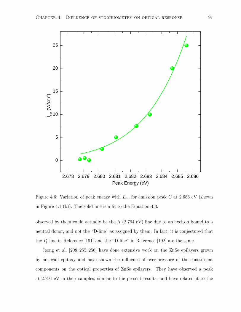
Chapter 4. Influence of stoichiometry on optical response 91
2 . 6 7 8 2 . 6 7 9 2 . 6 8 0 2 . 6 8 1 2 . 6 8 2 2 . 6 8 3 2 . 6 8 4 2 . 6 8 5 2 . 6 8 6
0
5
1 0
1 5
2 0
2 5I ex
c (W/cm
2 )
P e a k E n e r g y ( e V )
Figure 4.6: Variation of peak energy with Iexc for emission peak C at 2.686 eV (shown
in Figure 4.1 (b)). The solid line is a fit to the Equation 4.3.
observed by them could actually be the A (2.794 eV) line due to an exciton bound to a
neutral donor, and not the “D-line” as assigned by them. In fact, it is conjectured that
the I∗2 line in Reference [191] and the “D-line” in Reference [192] are the same.
Jeong et al. [208, 255, 256] have done extensive work on the ZnSe epilayers grown
by hot-wall epitaxy and have shown the influence of over-pressure of the constituent
components on the optical properties of ZnSe epilayers. They have observed a peak
at 2.794 eV in their samples, similar to the present results, and have related it to the
Chapter 4. Influence of stoichiometry on optical response 92
bound excitons at a neutral donor (D0X). Even though they have observed the peak
at same energy position in the spectrum as reported here, they found different binding
energies for the bound exciton and the donor because of the different values of the Eg
and exciton binding energy that they were using. They assigned the peak to excitons
bound to VSe at a neutral donor, and have found EBX = 14 meV, and the binding energy
to be ED = 70 meV. In the present case, the peak at 2.794 eV is assigned to the same
origin, corresponding to EBX = 7 meV, and a donor binding energy of ED = 35 meV.
This appears reasonable as it was shown by Morimoto [174] that in their Zn-rich films,
the Se-vacancy (VSe) is the main donor. Also, based on their analysis, Roppischer have
ruled out the possibility of Zni as the responsible centre [191].
Two donor-acceptor pair related recombinations were observed in presently studied
samples at 2.714 eV and 2.686 eV. These observed DA pair bands are similar to those
identified earlier by Dean and Merz [155] (labelled as R and Q bands, respectively), and
also by Swaminathan and Greene [159]. According to Iida [257] and Dean and Merz [155],
the increase in energy is 2.0 meV and 3.5 meV per decade of increase in Iexc, based on
their PL measurements, while Ikeda et al. [258] have reported 1.13 meV increase per
decade increase in electrical injection. In ZnSe NW samples studied here, it was noticed
that the change in energy is smaller at weak Iexc, and increases as the Iexc is increased.
This change is ≈1 meV at the lowest Iexc to ≈4 meV at the highest Iexc. Table 4.1 lists
the fit parameters obtained from a fit of experimental data to Equation 4.3. In Table 4.1,
EB = hνB − hν∞(= e2/εRB). As above, the value of the band-gap of ZnSe is Eg = 2.822
eV [155, 237] and an exciton binding energy of EFX = 21 meV [252] was used for these
calculations.
Zacks and Halperin [237] calculated hν∞ = 2.691 eV and hνB = 2.750 eV, and the
values of hν∞ = 2.693 eV and hνB = 2.746 eV found here are in very good agreement
with their values. They used the model they developed [237] (Equation 4.3) to analyze
the experimental data for the R band spectra of Dean and Merz [155]. Also, the present

Chapter 4. Influence of stoichiometry on optical response 93
Table 4.1: Table showing the values of different fitting parameters of Equation 4.3
Ep (eV) hν∞ (eV) hνB (eV) ED + EA (meV) EB (meV)
2.714 2.693 2.746 129 53
2.686 2.656 2.739 166 83
value for the sum of ionization energies of the donor and acceptor, for emission band B
(2.714 eV) of 129 meV, is very similar to their value of 131 meV. Dean and Merz [155]
themselves gave a value of EA + ED of 141 meV, with hν∞ = 2.681 eV. Iida [257] has
given a value of ED = 26 ± 3 meV and EA = 100 ± 1 meV, giving ED + EA of 126 ± 4
meV, which is similar to the value of 129 meV reported here. Ikeda et al. [258] have
proposed a value of ED + EA > 137 meV, which is not in agreement with the values
found by Zacks and Halperin [237], and Iida [257], but agrees well with the value found
by Dean and Merz [155].
An estimate of the shallow hydrogenic donor energy can be made by using ED =
(13.6/ε)(RH/RB) [237], where RH = 0.529 A is the Bohr radius for hydrogen and RB in
turn can be obtained from EB. For peak B, EB = 53 meV gives RB of 31.3 A, and for
peak C, EB = 83 meV gives RB = 20.0 A. According to the hydrogenic model, donor
binding energy ED = (m∗ee4/2~2ε2) = (13.6/ε2)(m∗e/m0), where (m∗e/m0) is the relative
effective mass of electron at the donor. Using (m∗e/m0) = 0.17 [252,259] and ε = 8.66 [252]
at liquid He temperature, ED = 30.8 meV. Similarly, the hydrogenic acceptor binding
energy is 136 meV using m∗h/m0 = 0.75 [252]. For peak B at 2.714 eV, ED = 26.5 meV,
or within the accuracy of experiments, 27 ± 1 meV, which is close to the hydrogenic
energy of 30.8 meV. Also, the present value of ED = 27± 1 meV is similar to that found
by Iida [257] (26± 1 meV) and Zacks and Halperin [237] (30 meV). The binding energy
of this donor is similar to the binding energies for group-III and group-VII donors, such
as Al(26.3 meV), Cl(26.9 meV), Ga(27.9 mev), In(28.9 meV) and F(29.3 meV) [158]. It
is unlikely that group-III and group-VII elements are involved, as excitonic lines related

Chapter 4. Influence of stoichiometry on optical response 94
to any group-III or group-VII element were not observed. Furthermore, post-growth
annealing treatments on NW samples similar to the ones studied here have shown [72]
that the near band-edge luminescence at room temperature almost completely disappears
when the NWs were annealed in a Se-atmosphere. The near band-edge luminescence is
recovered when the samples are annealed in a Zn-atmosphere. This suggests that the
donor can not be a group-III or group-VII element, as annealing in a Se-atmosphere
would not change the luminescence due to this donor. It is proposed that the shallow
donor is a simple native defect of Zn or Se, or a complex defect of the native defects.
Recently, Ivanova et al. [260] have reported on the interaction of intrinsic defects with Al
donors, and it is a possibility that in present ZnSe NWs, the donors and acceptors are
related to the complex defects of native defects with impurities. The acceptor binding
energy is 102 meV, which is again in good agreement with the values found by Iida [257]
(100 ± 1 meV) and Zacks and Halperin [237] (101 meV). The present value of acceptor
binding energy agrees well with the values reported in literature [7].
For peak C at 2.686 eV, RB = 20.0 A giving ED = 41.5 meV, which does not
match the shallow donor hydrogenic energy. The value for the acceptor energy is thus
EA = 124.5 eV. However, the value of ED +EA = 166 meV is similar to the value found
by Dean and Merz [155] for their Q band (150 meV). One possibility is that the acceptor
is a hydrogenic impurity, while the other possibility is that neither of donor and acceptor
are hydrogenic impurities. The value of acceptor energy can be found by measuring PL
at higher temperatures, since the DA pair band evolves towards the free-to-bound (FB)
recombination as the temperature is increased. The energy for the emitted photon in a
FB transition, EFB, is given by [261]
EFB = Eg − EA + Ek (4.4)
where Ek = kBT is the kinetic energy of the free electron. kB is the Boltzmann constant
and T is the temperature. PL measurements were performed at 40 K and 75 K, and
EFB was found to be EFB/40K = 2.682 eV and EFB/75K = 2.679 eV. Ek corresponding to

Chapter 4. Influence of stoichiometry on optical response 95
these temperatures is Ek/40K = 3.4 meV and Ek/75K = 6.5 meV, giving EA/40K = 139.4
meV and EA/75K = 138.5 meV. Eg at 40 K and 75 K were found using Varshni’s [262]
semiempirical relation with α = 7.3 × 10⁻⁴ eV/K and β = 295 K [263]. These results
indicate that the acceptor binding energy for band C is about 139 meV, which gives
a donor binding energy of 27 meV. This value of EA is close to the shallow acceptor
hydrogenic energy, and the value of ED is also in very good agreement with the shallow
donor hydrogenic energy. Since the EA values agree for two different measurements at
different temperatures, it is believed that the correct values are EA = 139 meV and
ED = 27 meV. The donor and acceptor must thus be assigned again to the defects,
simple or complex, of the native defects of the crystal, based on the earlier arguments.
Morimoto [264] have observed two FB peaks at 2.698 eV and 2.680 eV in PL at 77 K of
their MOCVD grown ZnSe samples, and have reported EA values of 110-114 meV and
128-130 meV, respectively. It is suggested that these two FB peaks are actually bands B
and C, respectively, observed in ZnSe NW samples studied here, and the reported values
of EA are similar to their values.
The peak D at 2.603 eV was first observed by Dean [163] in their MOCVD grown ZnSe
samples. They related this peak to the recombination at extended defects, where strong
delocalization of binding potential takes place. This perturbation in the potential due
to extended defects is associated with the emission at 2.605 eV, labelled as Y-line [163].
Taguchi et al. [265] observed the Y-line at 2.61 eV and its phonon replica at 2.58 eV. In
the present results, the Y-line emission at 2.603 eV would give the energy of first-phonon
replica to be 2.572 eV. The error in peak fitting procedures for peaks A, B, C and D is
about 0.1 meV, while this error for peak E is 4.8 meV because of its weak intensity. Peak
E appears only as a shoulder at the low-energy side of the spectrum in Figure 4.1 (b),
and it is reasonable to think that this is the first-LO phonon replica of the Y-line peak D.
Y-line emission has been discussed in the literature on ZnSe epilayers grown by different
methods [266–270], and recently in NWs as well [103, 106]. It has been suggested [267]

Chapter 4. Influence of stoichiometry on optical response 96
that this line is strong in intensity for samples with low background impurities and high
density of structural defects. In the present samples, the strength of Y-line with respect
to the donor-bound exciton line (RY = ID0X/IY ) changes with Iexc from 0.1 to 3.57, and
follows a super-linear dependence with the Iexc with a scaling coefficient of 1.19. ID0X
and IY are the integrated PL intensities of the D0X emission and the Y-line, respectively.
In present samples, it is believed that the concentration of impurities is very low, so that
the cause of Y-line emission would be the structural defects. It is also to be noted that
this emission is not seen from all areas of the sample, but only at certain areas. This
indicates that the sample is inhomogeneous, and that the structural defects are localized
at certain areas only, i.e. not all NWs. The NWs themselves are of good crystalline
quality [72,77,81], but there can be sources of these defects in the samples. For example,
the residue (or precipitates) deposited on the substrate surface can consist of structural
defects. Also, it is quite possible that in the ensemble of NWs, there is a distribution
of NWs with different crystalline quality or different concentration of structural defects
that give rise to the Y-line emission.
The LTPL spectrum for the NWs grown in conditions of excess Se (shown in Figure 4.2
(a)) shows features in contrast to those in the LTPL spectrum from NWs grown in the
conditions of excess Zn (shown in Figures 4.1 (a,b)). The LTPL spectrum from excess
Se NWs show that the PL is dominated by deep-level (DL) luminescence at 2.27 eV and
1.96 eV, while no exciton-related peaks were observed in the near band-edge region of
the spectrum (Figure 4.2 (b)). In earlier works by Roppischer et al. [191], they found
that when ZnSe crystals were annealed in a Se atmosphere, the donor-bound exciton
peaks related to VSe disappeared and new exciton-related peaks related to VZn appeared.
These VZn-related recombination lines were associated with the excitons bound to deep
neutral acceptors where VZn acts as an acceptor. The DL emission can be related to
the vacancies of Zn and this assignment can be understood as follows. For ZnSe NWs
prepared under excess Zn, the concentration of VZn is low, while those of VSe (which act

Chapter 4. Influence of stoichiometry on optical response 97
as donors) is higher, leading to a donor-bound exciton line. A low intensity of the DL
emissions in this case shows that VSe donors do not participate in these broad bands. In
NWs with excess Se, the concentration of VZn is higher and that of VSe is low. This results
in a strong intensity of the exciton lines related to VZn-acceptors, while the VSe-related
emission gets weaker or completely disappears [191]. In earlier works [271,272], the VZn-
related acceptor bound emission was found to be accompanied by the DL emissions. In
the present case however, the VZn-related exciton emission was not observed in NWs with
excess Se while strong DL emissions were seen. This is attributed to the participation of
VZn in the DL emissions. The absence of VZn-related exciton emission can be ascribed
to the un-optimum growth of NWs in conditions of excess Se, which leads to a poor
crystalline quality. Philipose et al [77, 78] have shown that NWs grown in conditions of
excess Se contain a high density of structural defects such as stacking faults.
4.4 Conclusions
In this chapter the results were presented on the PL from ZnSe NWs synthesized using
vapor-phase growth method under conditions of excess Zn and Se. Iexc-dependence of
PL from NWs grown under the conditions of excess Zn was analyzed in detail. A strong
peak related to an exciton bound to a neutral donor at VSe was observed at 2.794 eV.
The binding energy of the exciton to the neutral donor was found to be 7 meV, and
the binding energy of the neutral donor was found to be 35 meV. Two peaks related to
donor-acceptor pair recombination were observed at 2.714 eV and 2.686 eV. The binding
energies of both the donors were 27 ± 1 meV, while those of the acceptors were 102.5
and 139 meV respectively. These donors and acceptors were assigned to the complexes
formed by single native defects such as VSe, VZn, Sei and Zni with other native defects
or foreign impurities. Y-line emission and its LO-phonon replica were also observed. The
LTPL spectrum from ZnSe NWs grown under conditions of excess Se was also compared

Chapter 4. Influence of stoichiometry on optical response 98
with that from NWs grown under excess of Zn. It was found that the donor-bound
exciton line related to VSe in NWs with excess Zn was absent in the NWs with excess Se,
and no other exciton-related line was observed. The PL spectrum from NWs with excess
Se was dominated by deep-level emissions at 2.27 eV and 1.96 eV. These were related to
the presence of VZn in the NWs.

Chapter 5
Single zinc-blende ZnSe nanowires
5.1 Introduction
As discussed in Chapters 1 and 2, considerable effort has been devoted to the growth
of ZnSe NWs and understanding their fundamental optical properties. Despite this, de-
tailed optical characterization in terms of the identification of recombination centres in
ZnSe NWs is still lacking. Reports on the growth of ZnSe NWs usually include their
optical characterization using RTPL, mainly as a preliminary indicator of their optical
quality. There has been limited progress in understanding the optical response of ZnSe
NWs, particularly on individual NWs, using LTPL which can provide the information
needed to understand the underlying recombination mechanisms. ZnSe primarily crys-
tallizes in the ZB crystal structure, and ZB NWs obtained using VLS growth mechanism
are single crystalline. ZnSe NWs also form in the WZ crystal structure and in many
cases co-exist with the ZB NWs in the same as-grown samples. It was also discussed in
Chapter 2 that ZnSe NWs usually occur with other 1D-nanostructures such as nanorib-
bons, nanosaws, nanobelts, etc, in the same sample. RTPL and LTPL characterization
of ZnSe NWs reported in the literature has been on arrays of ZnSe NWs. These ev-
idently include contributions from NWs of different diameters, crystal structures, and
99
Chapter 5. Single zinc-blende ZnSe nanowires 100
other 1D-nanostructures. There has been no report so far correlating the recombination
mechanisms in ZB NWs with their single-crystalline microstructure.
This chapter presents the results on the optical characterization of individual ZB
NWs with a determination of their crystal structure using TEM, HR-TEM and SAD,
and is organised as follows. First, the LTPL spectrum from a single ZB NW is presented,
and the origin of the different peaks observed is discussed. The optical response of other
single ZB NWs measured using LTPL is also presented. The peak positions (Ep) and
linewidths (Γp) (defined as the FWHM) of peaks in the PL spectrum from a single ZB
NW are then compared with those from a bundle of ZB NWs. The identification of the PL
peaks is further supported by using the dependence of PL on temperature and excitation
intensity. Quantitative information on the energy band gap, and recombination lines is
also obtained using the analysis of the dependence of PL on temperature. Details on the
theoretical models used in this analysis are given in the Appendix C.2.2.
5.2 Results and Discussion
5.2.1 Characterization of single ZB ZnSe NWs
Six individual ZB NWs were characterized by both optical and structural characterization
methods. Five of these were selected from the same as-grown ZnSe NW sample. In this
section the structural characterization results are presented on one ZB NW (labelled as
ZB-NW-1). The results on optical characterization using LTPL are presented for ZB-
NW-1 and three other single NWs (labelled ZB-NW-2, 3 and 4). For the determination
of the crystal structure, HR-TEM micrographs were taken at several locations along the
length of the NWs. The SAD patterns were acquired from larger areas at a few locations
along the length of the NWs. It was found that the majority of ZB NWs were defect-free
and single-crystalline.

Chapter 5. Single zinc-blende ZnSe nanowires 101
HR-TEM characterization
Figure 5.1 (a) shows an overview TEM micrograph of ZB-NW-1 on the TEM grid, and
Figure 5.1 (b) shows a HR-TEM micrograph from an area of ZB-NW-1. Figure 5.1 (c)
shows a SAD pattern from an area of ZB-NW-1. The indexed diffraction spots in the SAD
pattern correspond to the ZB crystal structure. Indexed SAD patterns from other areas
of ZB-NW-1 also confirmed its ZB crystal structure. Figure 5.2 (a) shows a HR-TEM
micrograph from another area of ZB-NW-1. The FFT pattern shown in the Figure 5.2
(b) was acquired from the area highlighted (in red) in (a). The indexed spots in the FFT
pattern further highlight that the area selected for acquiring the FFT pattern on the
HR-TEM micrograph of ZB-NW-1 is single crystalline with a ZB crystal structure. The
TEM and HR-TEM micrographs, and indexed SAD and FFT patterns for ZB-NW-2 are
shown in Figures G.1, G.2 and G.3 in Appendix G which confirm a ZB crystal structure
for ZB-NW-2.
Low-temperature PL spectra
The LTPL spectrum (3.5 K) from ZB-NW-1 near the excitonic region is shown in Figure
5.3 acquired under the conditions of high throughput. Iexc and dslit are as indicated in the
Figure 5.3. The inset to Figure 5.3 shows a confocal PL image of ZB-NW-1 under laser
excitation with Iexc=12.7 W/cm2. The LTPL spectrum was fit to individual emission
peaks using Lorentzians, as shown. Two dominant peaks are observed at 2.785 eV and
2.780 eV, and their origin will be discussed first. In the literature on ZnSe single crystals
and epilayers, a recombination line near 2.783 eV has been reported on several occasions,
and labelled as Id1 [255,256,273–283] or Ideep1 [284–291] line. The lines related to excitons
bound to neutral acceptors, have usually been labelled as I1 lines. The Id1 (or Ideep1 ) line
is believed to originate from a deep neutral acceptor. This line has been assigned to two
origins in the past. Roppischer et al. [191] and Satoh and Igaki [271] related the Id1 line
to the vacancies of Zn (VZn), while Dean [272] and Dean et al. [292] suggested that the
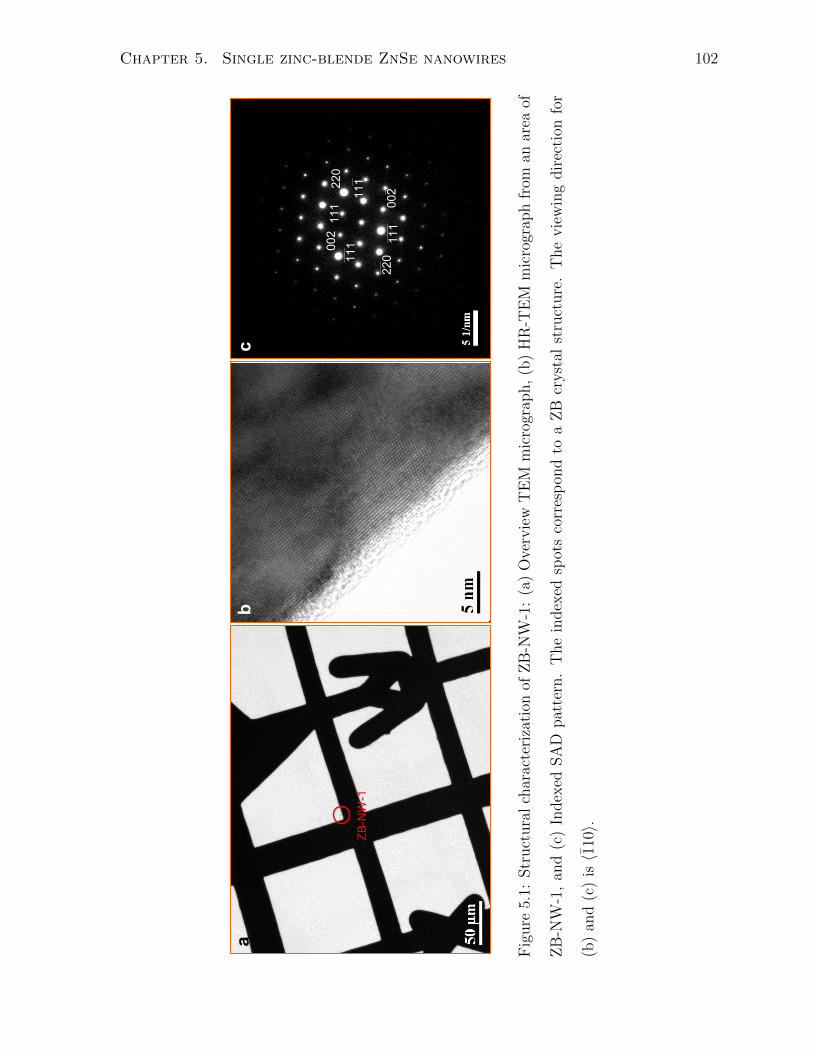
Chapter 5. Single zinc-blende ZnSe nanowires 102
ZB-NW-1
ab
c
111
111
220
220
002
002
111
111
Fig
ure
5.1:
Str
uct
ura
lch
arac
teri
zati
onof
ZB
-NW
-1:
(a)
Ove
rvie
wT
EM
mic
rogr
aph,
(b)
HR
-TE
Mm
icro
grap
hfr
oman
area
of
ZB
-NW
-1,
and
(c)
Index
edSA
Dpat
tern
.T
he
index
edsp
ots
corr
esp
ond
toa
ZB
cryst
alst
ruct
ure
.T
he
vie
win
gdir
ecti
onfo
r
(b)
and
(c)
is〈1
10〉.
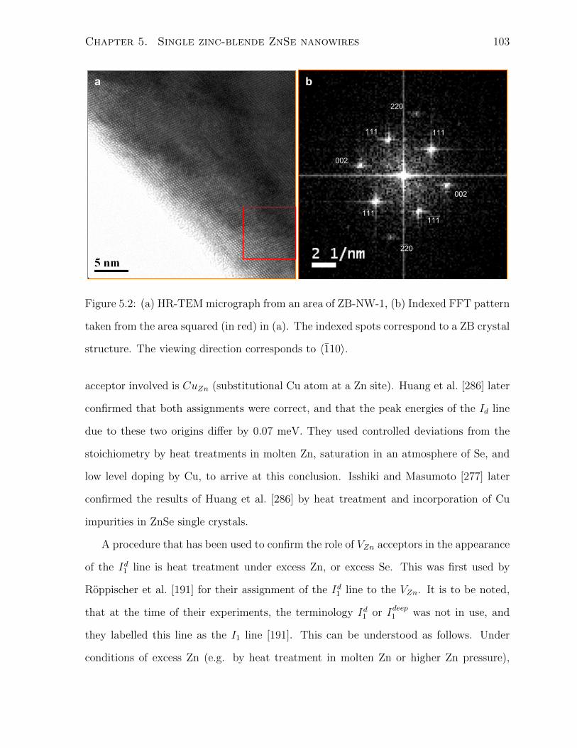
Chapter 5. Single zinc-blende ZnSe nanowires 103
a b
111
111
220
220
002
002
111
111
Figure 5.2: (a) HR-TEM micrograph from an area of ZB-NW-1, (b) Indexed FFT pattern
taken from the area squared (in red) in (a). The indexed spots correspond to a ZB crystal
structure. The viewing direction corresponds to 〈110〉.
acceptor involved is CuZn (substitutional Cu atom at a Zn site). Huang et al. [286] later
confirmed that both assignments were correct, and that the peak energies of the Id line
due to these two origins differ by 0.07 meV. They used controlled deviations from the
stoichiometry by heat treatments in molten Zn, saturation in an atmosphere of Se, and
low level doping by Cu, to arrive at this conclusion. Isshiki and Masumoto [277] later
confirmed the results of Huang et al. [286] by heat treatment and incorporation of Cu
impurities in ZnSe single crystals.
A procedure that has been used to confirm the role of VZn acceptors in the appearance
of the Id1 line is heat treatment under excess Zn, or excess Se. This was first used by
Roppischer et al. [191] for their assignment of the Id1 line to the VZn. It is to be noted,
that at the time of their experiments, the terminology Id1 or Ideep1 was not in use, and
they labelled this line as the I1 line [191]. This can be understood as follows. Under
conditions of excess Zn (e.g. by heat treatment in molten Zn or higher Zn pressure),

Chapter 5. Single zinc-blende ZnSe nanowires 104
2 . 6 5 2 . 7 0 2 . 7 5 2 . 8 0 2 . 8 5
I 1d’ -3LO
I 1d -3LO I 1d’ -2L
O I 1d -2LO
I 1d’ -1LO
L T P L - Z B - N W - 1 I 1
d l i n e I 1
d ’ l i n e S u m o f i n d i v i d u a l p e a k s
T e m p . = 3 . 5 K I e x c = 1 2 . 7 W / c m 2
d s l i t = 5 0 0 µm
PL In
tensity
(arb.
units)
E n e r g y ( e V )
4 . 5 m e V
I 1d -1LO
FX
Figure 5.3: Excitonic region of the LTPL spectrum (3.5 K) from ZB-NW-1 acquired
under the conditions of high-throughput. (Iexc and dslit are as indicated). The inset
shows a confocal PL image of ZB-NW-1 under laser excitation with an average Iexc=12.7
W/cm2. The diameter of pin-hole in the PL image is 5 µm. The LTPL spectrum was fit
to individual emission peaks using Lorentzians as shown.
the concentration of VZn is reduced, and the intensity of the Id1 line is therefore also
reduced [191, 276, 278–281, 284]. In many cases it was found that the Id1 line completely
disappears after Zn-treatment [191,255,274,275,277,284,286,288]. When the heat treat-
ment is carried out under conditions of excess Se, the concentration of VZn increases,

Chapter 5. Single zinc-blende ZnSe nanowires 105
and results in an increase in the intensity of the Id1 line [191, 271, 280, 282, 284, 288, 289],
or it reappears (if disappeared due to a prior Zn-treatment) [191, 255, 277, 284]. The
disappearance and reappearance of the Id1 line under different heat treatments has been
observed by several authors [191, 255, 277, 280, 284], and based on this observation, they
related the Id1 line to VZn acceptors [191, 277, 280, 284]. Any involvement of CuZn in the
Id1 line has also been effectively ruled out based on these observations. For example,
based on their LTPL experiments on samples annealed in Zn and Se atmospheres, Pohl
et al. [280] concluded that any role of Cu in the Id1 line can be excluded. Several au-
thors have also argued that the Id1 line is due either to VZn or complexes containing VZn
(VZn-complex) [271,280,284]. However, a clear distinction has not yet been established.
It is important to note that a wide range of energy positions of the Id1 line has been
reported in the literature, from 2.779 eV [188] to 2.7858 eV [273]. In some cases the
authors identified the line as the Id1 line without noting the peak position [274,275,277].
This is because of the characteristic strong LO-phonon coupling of the Id1 line. The Id1
line is known to occur with several LO-phonon replicas [191, 255, 274, 278, 279, 284, 286,
287, 289, 290]. Phonon-replicas of up to six orders have been reported for this line [291]
indicative of a strong LO-phonon coupling. Skromme et al. [293], for example, observed
a recombination line at 2.7823 eV, which is common to most reported energy positions of
the Id1 line. But they did not relate it to the Id1 line as they did not see any LO-phonon
replicas of this line in the PL spectrum.
Figures 5.4 (a,b) show the LTPL spectra (3.6 K) from ZB-NW-2 acquired under the
conditions of (a) high-throughput, and (b) high-resolution. The LTPL spectra (3.8 K)
taken using similar conditions from ZB-NW-3 are shown in the Figures 5.5 (a,b). It
is seen that the PL peaks similar to those in the LTPL spectrum from ZB-NW-1 are
observed for both ZB-NW-2 and 3. In the present case, the absence of Cu in ZnSe NWs
(grown using the vapor-phase transport method) was confirmed by their growth under
conditions of excess Zn and Se and subsequent LTPL experiments (see Chapter 4). The
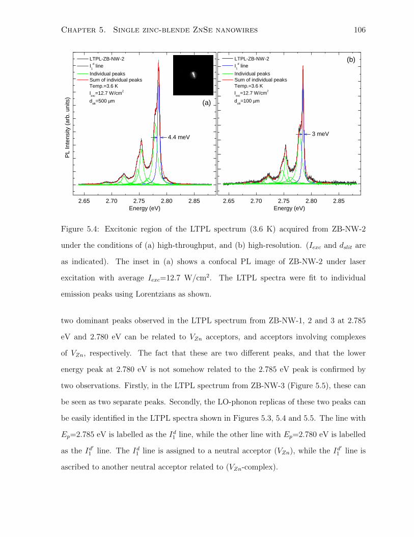
Chapter 5. Single zinc-blende ZnSe nanowires 106
2 . 6 5 2 . 7 0 2 . 7 5 2 . 8 0 2 . 8 5
( b )PL
Inten
sity (a
rb. un
its)
E n e r g y ( e V )
L T P L - Z B - N W - 2 I 1
d l i n e I n d i v i d u a l p e a k s S u m o f i n d i v i d u a l p e a k s
T e m p . = 3 . 6 K I e x c = 1 2 . 7 W / c m 2
d s l i t = 5 0 0 µm
4 . 4 m e V
( a )
2 . 6 5 2 . 7 0 2 . 7 5 2 . 8 0 2 . 8 5
L T P L - Z B - N W - 2 I 1
d l i n e I n d i v i d u a l p e a k s S u m o f i n d i v i d u a l p e a k s
T e m p . = 3 . 6 K I e x c = 1 2 . 7 W / c m 2
d s l i t = 1 0 0 µm
E n e r g y ( e V )
3 m e V
Figure 5.4: Excitonic region of the LTPL spectrum (3.6 K) acquired from ZB-NW-2
under the conditions of (a) high-throughput, and (b) high-resolution. (Iexc and dslit are
as indicated). The inset in (a) shows a confocal PL image of ZB-NW-2 under laser
excitation with average Iexc=12.7 W/cm2. The LTPL spectra were fit to individual
emission peaks using Lorentzians as shown.
two dominant peaks observed in the LTPL spectrum from ZB-NW-1, 2 and 3 at 2.785
eV and 2.780 eV can be related to VZn acceptors, and acceptors involving complexes
of VZn, respectively. The fact that these are two different peaks, and that the lower
energy peak at 2.780 eV is not somehow related to the 2.785 eV peak is confirmed by
two observations. Firstly, in the LTPL spectrum from ZB-NW-3 (Figure 5.5), these can
be seen as two separate peaks. Secondly, the LO-phonon replicas of these two peaks can
be easily identified in the LTPL spectra shown in Figures 5.3, 5.4 and 5.5. The line with
Ep=2.785 eV is labelled as the Id1 line, while the other line with Ep=2.780 eV is labelled
as the Id′
1 line. The Id1 line is assigned to a neutral acceptor (VZn), while the Id′
1 line is
ascribed to another neutral acceptor related to (VZn-complex).

Chapter 5. Single zinc-blende ZnSe nanowires 107
2 . 6 5 2 . 7 0 2 . 7 5 2 . 8 0 2 . 8 5
PL In
tensity
(arb.
units)
E n e r g y ( e V )
L T P L - Z B - N W - 3 I 1
d l i n e I n d i v i d u a l p e a k s S u m o f i n d i v i d u a l p e a k s
T e m p . = 3 . 8 K I e x c = 1 2 . 7 W / c m 2
d s l i t = 5 0 0 µm
4 . 5 m e V3 . 8 m e V
( a ) ( b )
2 . 6 5 2 . 7 0 2 . 7 5 2 . 8 0 2 . 8 5
L T P L - Z B - N W - 3 I 1
d l i n e I n d i v i d u a l p e a k s S u m o f i n d i v i d u a l p e a k s
T e m p . = 3 . 8 K I e x c = 6 . 4 W / c m 2
d s l i t = 1 0 0 µm
E n e r g y ( e V )
Figure 5.5: Excitonic region of the LTPL spectrum (3.8 K) acquired from ZB-NW-3
under the conditions of (a) high-throughput, and (b) high-resolution. (Iexc and dslit are
as indicated). The LTPL spectra were fit to individual emission peaks using Lorentzians
as shown.
The energy position of the LO-phonon replica of the m-th order (Ep,m) is given by
Ep,m = Ep −m~ωLO (5.1)
where Ep is the energy position of the zero-phonon line (ZPL) (m = 0), and ~ωLO is the
LO-phonon energy (∼31 meV in ZnSe [294]). The peaks at 2.755 eV, 2.723 eV and 2.692
are Id1 -1LO, Id1 -2LO and Id1 -3LO, respectively. Similarly, the peaks at 2.748 eV, 2.715
eV and 2.685 eV are Id′
1 -1LO, Id′
1 -2LO and Id′
1 -3LO, respectively. These are indicated by
arrows in Figure 5.3. The calculated intensity ratio of the intensity of the m-th order
LO-phonon replica (Im) to that of the ZPL (I(m=0)) is given by Hopfield’s relation [295]
as:
Im/I(m=0) = Nmph/m! (5.2)
where Nph is the average number of phonons emitted. The experimental and calculated

Chapter 5. Single zinc-blende ZnSe nanowires 108
intensity ratios of the LO-phonon replicas to the ZPL for the Id1 and Id′
1 lines are listed in
the Table 5.1 for ZB-NW-1, 2 and 3. (Table 5.1 also includes these ratios for LTPL from
a bundle of ZB NWs, to be discussed in the next section). The values in the columns
(2) and (4) corresponding to m=1 represent Nph in each case. As mentioned earlier,
several authors have reported on the observation of LO-phonon replicas of the Id1 line,
but their intensity ratios have not been reported in most cases. The values of intensity
ratios reported by Jiang et al. [287] are also included in the Table 5.1 for comparison.
Jiang et al. [287] found Nph of 0.45 for the Id1 line. It may be seen from the Table 5.1
that Nph for the Id1 is larger than that for the Id′
1 line. Also, the Nph are not identical for
the three NWs and the NW bundle which indicates different strengths of the LO-phonon
coupling in these NWs. These values are 0.53 < Nph < 0.7 for the Id1 line, and 0.25
< Nph < 0.42 for the Id′
1 line.
The peak with Ep=2.800 eV is related to the emission of free excitons (FX), and
labelled as FX in the Figure 5.3. The FX emission was also observed by various au-
thors in as-grown ZnSe samples [188,255,284] and in ZnSe samples after heat treatment
in the conditions of excess Zn [188]. This peak has been labelled in many cases as
Ex [255,271,274,275,284]. This assignment of the peak at 2.800 eV to FX is further con-
firmed using the dependence of PL on temperature later in this chapter. These results
indicate that the optical response of ZnSe NWs grown under stoichiometric conditions
(i.e. using stoichiometric ZnSe source and no further heat treatment) is dominated by
recombination related to native point defects (VZn and VZn-complex), and that the un-
intentional impurities play no role. The ZnSe NWs are therefore intrinsically Se-rich (or
Zn-deficient). Further, the Y-line (Ep=2.603 eV) which was observed in the PL from
an array of ZnSe NWs in the as-grown samples (see Chapter 4) was not observed in
the case of single ZB NWs. This can be seen in the Figures 5.3, 5.4 and 5.5 on LTPL
from ZB-NW-1, 2 and 3, respectively. This shows that the origin of the Y-line is due to
structural defects such as dislocations present in the undergrowth of polycrystalline ZnSe
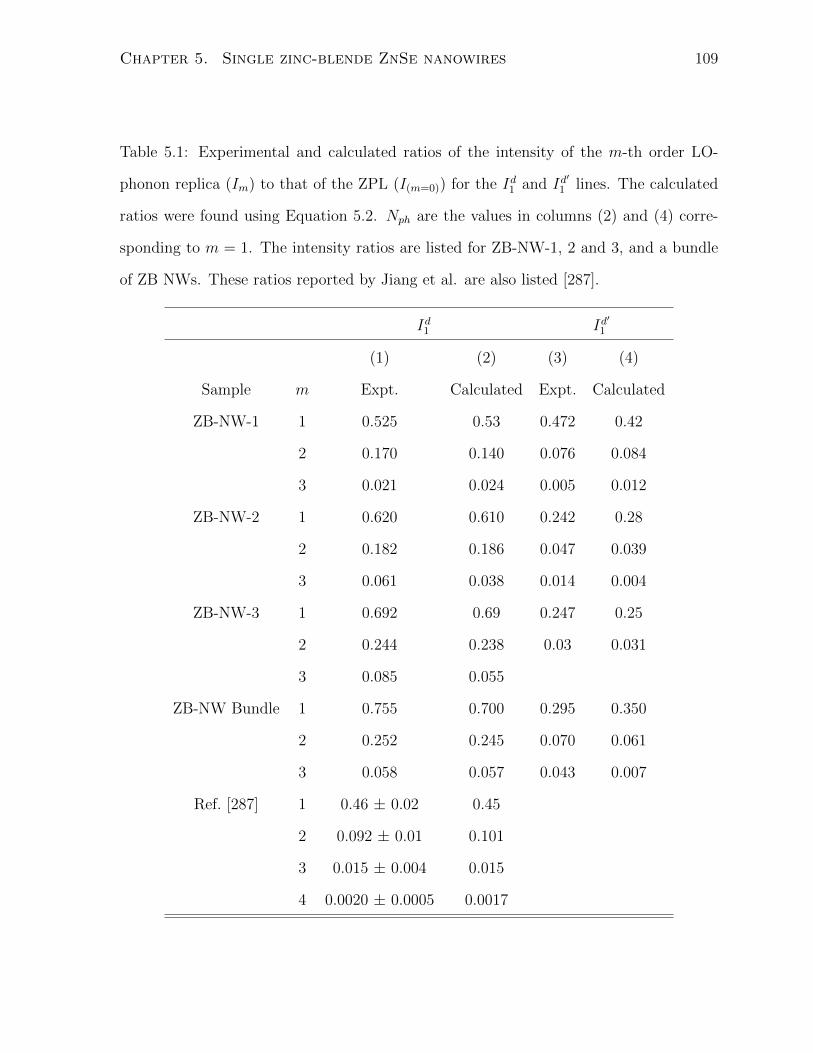
Chapter 5. Single zinc-blende ZnSe nanowires 109
Table 5.1: Experimental and calculated ratios of the intensity of the m-th order LO-
phonon replica (Im) to that of the ZPL (I(m=0)) for the Id1 and Id′
1 lines. The calculated
ratios were found using Equation 5.2. Nph are the values in columns (2) and (4) corre-
sponding to m = 1. The intensity ratios are listed for ZB-NW-1, 2 and 3, and a bundle
of ZB NWs. These ratios reported by Jiang et al. are also listed [287].
Id1 Id′
1
(1) (2) (3) (4)
Sample m Expt. Calculated Expt. Calculated
ZB-NW-1 1 0.525 0.53 0.472 0.42
2 0.170 0.140 0.076 0.084
3 0.021 0.024 0.005 0.012
ZB-NW-2 1 0.620 0.610 0.242 0.28
2 0.182 0.186 0.047 0.039
3 0.061 0.038 0.014 0.004
ZB-NW-3 1 0.692 0.69 0.247 0.25
2 0.244 0.238 0.03 0.031
3 0.085 0.055
ZB-NW Bundle 1 0.755 0.700 0.295 0.350
2 0.252 0.245 0.070 0.061
3 0.058 0.057 0.043 0.007
Ref. [287] 1 0.46 ± 0.02 0.45
2 0.092 ± 0.01 0.101
3 0.015 ± 0.004 0.015
4 0.0020 ± 0.0005 0.0017

Chapter 5. Single zinc-blende ZnSe nanowires 110
2 . 6 5 2 . 7 0 2 . 7 5 2 . 8 0 2 . 8 5
L T P L - Z B - N W - 1 I 1
d l i n e I n d i v i d u a l p e a k s S u m o f i n d i v i d u a l p e a k s
T e m p . = 3 . 7 K I e x c = 3 . 2 W / c m 2
d s l i t = 1 0 0 µmPL
Inten
sity (a
rb. un
its)
E n e r g y ( e V )
2 . 4 m e V
Figure 5.6: Excitonic region of the LTPL spectrum (3.7 K) from ZB-NW-1 acquired
under the conditions of high-resolution. (Iexc and dslit are as indicated). The inset
shows a confocal PL image of ZB-NW-1 under laser excitation with an average Iexc=12.7
W/cm2. The diameter of pin-hole in the PL image is 5 µm. The LTPL spectrum was fit
to individual emission peaks using Lorentzians as shown.
on the sample substrate, and is not related to the NWs at all. This is also to be expected
given the defect-free single-crystalline structure of the NWs which was confirmed by the
TEM, HR-TEM and SAD.
The binding energy of the excitons, EBX , related to the Id1 and Id′
1 lines can be
determined using EBX = Eg − EFX − Ep. The Ep for the FX line, equal to Eg − EFX ,
being experimentally known, can be used here. For the Id1 line, EBX = 2.800 − 2.785
Chapter 5. Single zinc-blende ZnSe nanowires 111
eV=15 meV. The ionization energy of the neutral acceptor (EA), using the rule of Halsted
and Aven [253], is then 150 meV. Similarly, for the Id′
1 line, EBX = 2.800− 2.780 eV=20
meV, and EA=200 meV. The Γp of the Id1 line is 4.5 meV in the LTPL spectrum acquired
under the conditions of high-throughput (shown in Figure 5.3). The LTPL spectrum from
ZB-NW-1 acquired under the conditions of high-resolution is shown in Figure 5.6. The
spectrum in this case was fit to six individual emission peaks using Lorentzians. The Γp
of the Id1 line at 2.785 eV is 2.4 meV, which is significantly narrower than that shown in
Figure 5.3 (4.5 meV). It may also be noticed that only the first order LO-phonon replica
of the Id1 and Id′
1 lines can be seen in the Figure 5.6, and the reasons for this have been
explained in detail in Chapter 3 in context of the conditions used for the acquisition of
PL spectra with high-resolution.
5.2.2 Comparison with an ensemble of ZB NWs
A bundle of ZB NWs on the TEM grid was selected using an iris (a variable aperture
pin-hole) for the LTPL experiments. A bundle of NWs is distinguished from an array
of NWs in that the bundle contains far fewer number of NWs than the array. This is
because the area selected on the sample (i.e. the TEM grid) with an iris, and used for
the collection of PL signal is much smaller than that of an array of NWs without the
use of an iris. It is estimated that about 5-10 NWs contribute to the PL signal in this
bundle. This can be seen by comparing the confocal PL image of the NW bundle (shown
in the inset of Figure 5.7) with that of the ZB-NW-1 and 2 (inset of Figures 5.3 and
5.4) (all at the same magnification). Since no structural characterization was possible
on this bundle of NWs lying on the TEM grid bar, it was assumed that it consists of
ZB NWs, possibly including 1D-nanostructures other than NWs such as nanoribbons.
The assumption that the NWs in this bundle are all ZB is reasonable since other NWs
studied from this sample (and from the same TEM grid) were all single-crystalline ZB,
including ZB-NW-2 and ZB-NW-3.

Chapter 5. Single zinc-blende ZnSe nanowires 112
2 . 6 5 2 . 7 0 2 . 7 5 2 . 8 0 2 . 8 5
PL In
tensity
(arb.
units)
E n e r g y ( e V )
L T P L - Z B - N W - B u n d l e I 1
d l i n e I n d i v i d u a l p e a k s S u m o f i n d i v i d u a l p e a k s
T e m p . = 3 . 9 K I e x c = 3 . 2 W / c m 2
d s l i t = 5 0 0 µm
5 . 3 m e V
2 . 6 5 2 . 7 0 2 . 7 5 2 . 8 0 2 . 8 5
L T P L - Z B - N W - B u n d l e I 1
d l i n e I n d i v i d u a l p e a k s S u m o f i n d i v i d u a l p e a k s
T e m p . = 3 . 9 K I e x c = 3 . 2 W / c m 2
d s l i t = 1 0 0 µm
E n e r g y ( e V )
4 . 3 m e V
( a )
( b )
Figure 5.7: Excitonic region of the LTPL spectrum (3.9 K) from a bundle of ZB NWs
acquired under the conditions of (a) high-throughput, and (b) high-resolution. (Iexc and
dslit are as indicated). The inset in (a) shows a confocal PL image of the bundle of ZB
NWs under laser excitation with average Iexc=12.7 W/cm2. The LTPL spectra were fit
to individual emission peaks using Lorentzians as shown.
The excitonic region of the LTPL spectrum (3.9 K) from this bundle of ZB NWs
is shown in Figure 5.7 acquired under the conditions of (a) high-throughput, and (b)
high-resolution. It may be observed that the conditions of acquisition (Iexc and dslit) are
similar to those for ZB-NW-1 (Iexc is different in (a)). Both spectra were fit to individual
emission peaks using Lorentzians, as shown. Inset in Figure 5.7 shows the confocal PL
image of the bundle of NWs selected using an iris under laser excitation with average Iexc
of 3.2 W/cm2. The Ep for the different peaks observed were found to be similar to those
in the LTPL spectra from ZB-NW-1, 2 and 3, and no additional peaks were noticed.
This further confirms the assumption that all NWs in the bundle are single-crystalline
ZB. The Γp of the Id1 line obtained are 5.3 meV and 4.3 meV under the conditions of
high-throughput and high-resolution, respectively. These are larger than the Γp of the
Chapter 5. Single zinc-blende ZnSe nanowires 113
Id1 line in LTPL from ZB-NW-1, 2 and 3 under similar conditions. It was discussed in
Chapter 3 that the Γp observed in the PL spectra from an array of NWs are larger than
those in the PL from single NWs. This is similar to the observation by Wischmeier et
al. [210] where they observed the Γp from an array of ZnO NWs larger by 0.2-0.5 meV
than those from single ZnO NWs for excitonic emission lines. The broadening of the Γp
in the present case is however larger than they reported, i.e. 0.8 and 1.9 meV for the
two conditions (when comparing Γp of the Id1 line in the case of the bundle of ZB NWs
and ZB-NW-1). Wischmeier et al. [210] related the broadening of the exciton emission
lines in PL from an array of NWs to the ensemble averaging of the PL signal over 100
NWs with varying diameters, morphologies and crystalline quality. The same argument
can be used to explain the broadening of the Id1 line in the LTPL from the bundle of ZB
ZnSe NWs. The Γp of the Id1 line in the LTPL spectra from ZB-NW-2 and ZB-NW-3
acquired under the conditions of high-resolution are 3 meV and 3.5 meV, respectively
(see Figures 5.4 and 5.5). These are larger than the Γp of the Id1 line from ZB-NW-1 (2.4
meV under similar conditions). This indicates that different NWs in the sample exhibit
slightly different Γp of the exciton emission lines (Id1 line in this case). Based on this,
another possible explanation for the observed broadening of the Id1 line in PL spectra
from the bundle of NWs could be that the measured Γp is limited by the NW with the
largest Γp of the Id1 line.
However, even narrower emission lines were observed in the PL from other ZnSe
NWs. These were not taken from the same sample as for ZB-NW-1, 2 and 3. Figures 5.8
(a,b) show the LTPL spectra from ZB-NW-4 (whose structural characterization was not
possible because it was on a Si substrate). Both spectra were fit to individual emission
peaks and the Id1 line is shown in the Figures 5.8 (a,b). The Γp of the Id1 lines were found
to be (a) 1.5 and (b) 1.6 meV. The Γp of the excitonic emission lines close to 1 meV
were also observed in the LTPL from single ZnSe nanoribbons. These are the narrowest
Γp’s reported so far for exciton emission lines in ZnSe NWs. These are also significantly
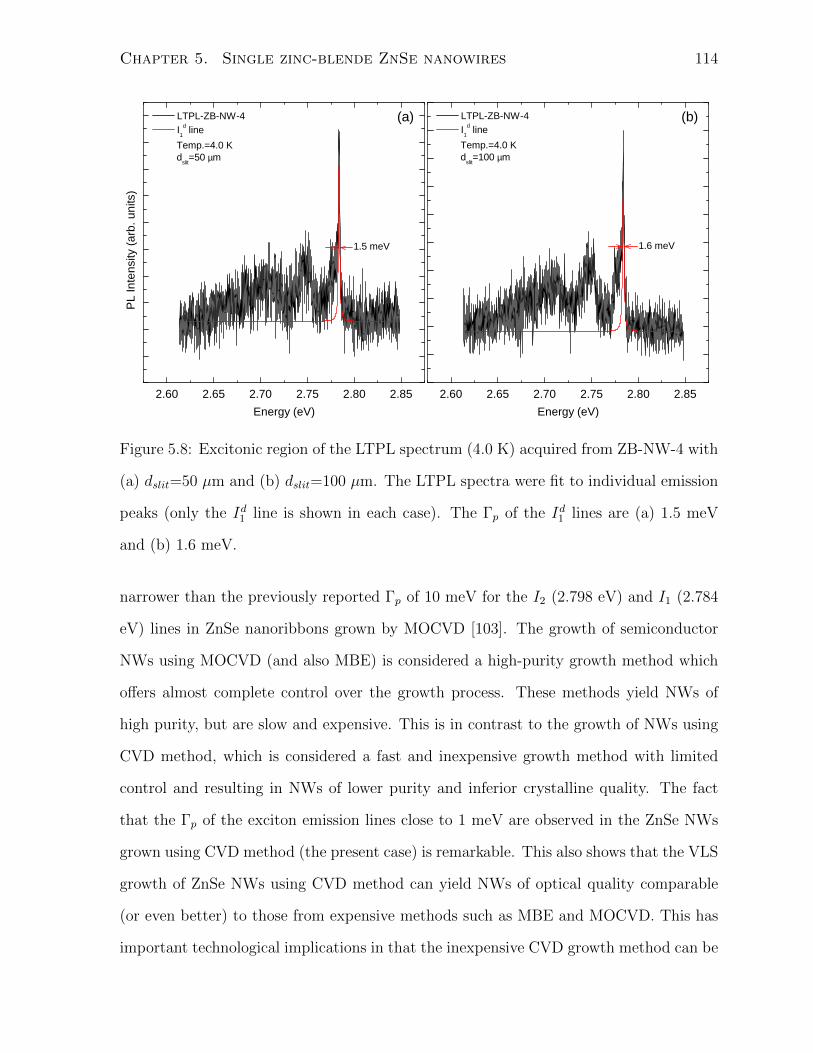
Chapter 5. Single zinc-blende ZnSe nanowires 114
2 . 6 0 2 . 6 5 2 . 7 0 2 . 7 5 2 . 8 0 2 . 8 5
PL In
tensity
(arb.
units)
E n e r g y ( e V )
L T P L - Z B - N W - 4 I 1
d l i n e T e m p . = 4 . 0 K d s l i t = 5 0 µm
1 . 5 m e V
2 . 6 0 2 . 6 5 2 . 7 0 2 . 7 5 2 . 8 0 2 . 8 5
( b )
1 . 6 m e V
L T P L - Z B - N W - 4 I 1
d l i n e T e m p . = 4 . 0 K d s l i t = 1 0 0 µm
E n e r g y ( e V )
( a )
Figure 5.8: Excitonic region of the LTPL spectrum (4.0 K) acquired from ZB-NW-4 with
(a) dslit=50 µm and (b) dslit=100 µm. The LTPL spectra were fit to individual emission
peaks (only the Id1 line is shown in each case). The Γp of the Id1 lines are (a) 1.5 meV
and (b) 1.6 meV.
narrower than the previously reported Γp of 10 meV for the I2 (2.798 eV) and I1 (2.784
eV) lines in ZnSe nanoribbons grown by MOCVD [103]. The growth of semiconductor
NWs using MOCVD (and also MBE) is considered a high-purity growth method which
offers almost complete control over the growth process. These methods yield NWs of
high purity, but are slow and expensive. This is in contrast to the growth of NWs using
CVD method, which is considered a fast and inexpensive growth method with limited
control and resulting in NWs of lower purity and inferior crystalline quality. The fact
that the Γp of the exciton emission lines close to 1 meV are observed in the ZnSe NWs
grown using CVD method (the present case) is remarkable. This also shows that the VLS
growth of ZnSe NWs using CVD method can yield NWs of optical quality comparable
(or even better) to those from expensive methods such as MBE and MOCVD. This has
important technological implications in that the inexpensive CVD growth method can be

Chapter 5. Single zinc-blende ZnSe nanowires 115
used to synthesise NWs with excellent optical quality on a large industrial scale. With
respect to the literature on other II-VI and III-V compound semiconductor NWs, Γp
close to 1-2 meV reported here compare favourably with the narrowest Γp reported (∼1
meV) [211–216]. (See also Section 2.3.2).
5.2.3 Dependence of PL on temperature
PL from ZB-NW-3 was recorded as a function of the sample temperature. Figure 5.9
shows the change in PL as the temperature is increased from 4 K to RT. Each of these
spectra were fit to individual PL peaks, and values obtained for the Ep, Γp and IPL
are discussed below. It was observed that the intensity of the Id1 and Id′
1 exciton lines
diminish rapidly as the temperature is increased (also referred to as quenching). At
a temperature around 50 K, the Id1 and Id′
1 emissions become quite weak. At the same
time, the FX emission becomes the dominant emission as the temperature is increased. At
higher temperatures FX emission merges with the emission related to the recombination
of electrons and holes in the conduction and the valence bands, respectively (free carrier
recombination).
The Ep of the FX emission can be used to determine the dependence of the Eg on
temperature. This is because the FX emission energy follows the Eg as the temperature is
increased, up to higher temperatures before the free excitons dissociate into free carriers
by the thermal energy. Figure 5.10 shows the change in Ep of the FX emission (for
ZB-NW-3) with the temperature. The dependence of Eg on temperature is described in
terms of the semi-empirical Varshni’s equation [262] given by:
Eg(T ) = Eg(0)− αT 2
β + T(5.3)
where α and β are the fitting constants. α can be considered to represent the high-
temperature limit of the temperature gradient (dEg/dT ) of Eg, and β has been related
to the Debye temperature θD for the crystal [262]. The solid line in Figure 5.10 is a fit to
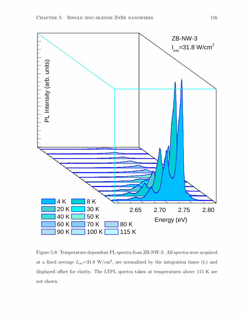
Chapter 5. Single zinc-blende ZnSe nanowires 116
2 . 6 5 2 . 7 0 2 . 7 5 2 . 8 0 4 K 8 K 2 0 K 3 0 K 4 0 K 5 0 K 6 0 K 7 0 K 8 0 K 9 0 K 1 0 0 K 1 1 5 K
PL In
tensity
(arb.
units)
E n e r g y ( e V )
Z B - N W - 3I e x c = 3 1 . 8 W / c m 2
Figure 5.9: Temperature dependent PL spectra from ZB-NW-3. All spectra were acquired
at a fixed average Iexc=31.8 W/cm2, are normalized by the integration times (ti) and
displayed offset for clarity. The LTPL spectra taken at temperatures above 115 K are
not shown.

Chapter 5. Single zinc-blende ZnSe nanowires 117
the Equation 5.3, and the parameters obtained from the fit are listed in Table 5.2. The
same parameters previously reported by other authors on ZnSe single crystals and thin-
films are also listed in the Table 5.2 for comparison. The peak positions of the PL peaks
for which these parameters were reported are also listed in the Table 5.2 under Eg(0).
The parameters α and β are found to be in excellent agreement with the previously
reported values. This confirms the assignment of the PL peak at 2.800 eV to the free
excitons. Further, this also shows that the temperature gradient (dEg/dT ) (high-T limit)
in ZB NWs is similar to that in ZnSe single crystals and thin-films.
Table 5.2: Values of the fit parameters of the Varshni’s equation (Equation 5.3) which
describes the temperature dependence of the Eg. (See Figure 5.10). The values reported
previously by other authors are also listed for comparison. A fitting error of 0 indicates
error of the order of 10−5 eV.
Eg(0) α β Source
(eV) (10−4 eV/K) (K)
FX, 2.799 ± 0 8.9 ± 0.7 361.5 ± 44.8 Expt.
2.794 8.59 350.0 [296]
2.797 8.59 350.0 [297]
2.804 eV 8.59 405 [283,298]
2.800 ± 0.005 7.3 ± 0.4 295 ± 35 [263]
The temperature dependence of the direct Eg is also described by a Bose-Einstein
type expression [263,299]:
Eg(T ) = Eg(0)− 2αB[exp
(θBT
)− 1
] (5.4)
where αB represents the strength of the exciton-average phonon interaction, and θB
corresponds to the average phonon temperature. The dashed line in Figure 5.10 is a fit to

Chapter 5. Single zinc-blende ZnSe nanowires 118
0 5 0 1 0 0 1 5 0 2 0 0 2 5 02 . 7 0
2 . 7 2
2 . 7 4
2 . 7 6
2 . 7 8
2 . 8 0 Z B - N W - 3 - E x p t .
E p = 2 . 8 0 0 e V F i t F i t
Energ
y (eV
)
T e m p e r a t u r e ( K )
Figure 5.10: Variation in PL peak energy of the FX emission (Ep=2.800 eV) (for ZB-
NW-3) with temperature. The solid and dashed lines are fits to the Equation 5.3 and
5.4, respectively.
Equation 5.4 and the obtained fit parameters are listed in the Table 5.3. These parameters
as reported by Malikova et al. [263] are also listed in the Table 5.3 for comparison. The
agreement between the two is good. The change in Ep for the Id1 and Id′
1 lines at 2.785 eV
and 2.780 eV, respectively, were also fit to these relations. However, a fit to the Varshni’s
equation (Equation 5.3) did not converge in both cases (unless one parameter was kept
fixed). This can be attributed to the smaller temperature range for which the values
of the Ep were available, because the Id1 emission was not observed above 150 K and
the Id′
1 line disappeared near 80 K. The Varshni’s equation describes the temperature

Chapter 5. Single zinc-blende ZnSe nanowires 119
0 2 0 4 0 6 0 8 0 1 0 0 1 2 0 1 4 0 1 6 02 . 7 4
2 . 7 5
2 . 7 6
2 . 7 7
2 . 7 8
2 . 7 9En
ergy (
eV)
E n e r g y ( e V )
Z B - N W - 3 - E x p t . E p = 2 . 7 8 5 e V
F i t
0 2 0 4 0 6 0 8 0
( b )
Z B - N W - 3 - E x p t . E p = 2 . 7 8 0 e V
F i t
E n e r g y ( e V )
( a )
Figure 5.11: Variation in PL peak energies for the (a) Id1 and (b) Id′
1 lines (for ZB-NW-3)
with temperature. The solid line are fits to the Equation 5.4.
dependence of the Eg in a temperature range from low-temperatures to the RT. The
fit to this equation did not converge because the experimental data was in a smaller
temperature range only. The change in Ep for the Id1 and Id′
1 lines with the temperature
are shown in the Figures 5.11 (a) and (b), respectively. The Ep for both lines were fit to
the Equation 5.4 (solid lines), and the fit parameters are listed in Table 5.3. In the case
of the Id1 line, the parameters αB and θB are in good agreement to those obtained for
the FX emission. However, for the Id′
1 line the agreement for these parameters with the
FX emission and the Id1 lines is not so good, the fit itself is however as good as for the
Id1 line (based on the residuals). This shows different behaviour for the Id1 and Id′
1 lines
with temperature.
The temperature dependence of the Γp/2 (half-width at half-maximum, HWHM) of
the exciton emission in direct Eg semiconductors is expressed by the relation [300]:

Chapter 5. Single zinc-blende ZnSe nanowires 120
Table 5.3: Values of the fit parameters of the Bose-Einstein type expression (Equation 5.4)
which describes the temperature dependence of the direct Eg. (See Figures 5.10 and 5.11
(a,b)). The values reported by Malikova et al. [263] are also listed for comparison. A
fitting error of 0 indicates error of the order of 10−5 eV.
Eg(0) αB θB Source
(eV) (meV) (K)
FX emission
2.797 ± 0 56.5 ± 4.7 209.3 ± 11.6 Expt.
2.800 ± 0.005 73 ± 4 260 ± 10 [263]
Id1 and Id′
1 emissions
Id1 , 2.785 ± 0 59.4 ± 11.1 201.9 ± 20.1 Expt.
Id′
1 , 2.779 ± 0 41.1 ± 21.4 141.4 ± 34.0 Expt.
Γp(T )/2 = Γinh + γthT +ΓLO[
exp
(θLOT
)− 1
] (5.5)
where each term on the right in the expression represents a different broadening mech-
anism. The first term (Γinh) is due to the intrinsic effects and represents the inhomo-
geneous broadening, including the instrumental broadening. It is to be noted that Γinh
is independent of the temperature. The second term is related to the lifetime broad-
ening due to exciton-acoustic phonon interactions, where γth is a constant representing
the acoustic phonon coupling. The third term corresponds to the exciton-LO phonon
interaction, where ΓLO is the strength of the exciton-LO-phonon coupling and θLO is
the LO-phonon temperature (or the temperature corresponding to LO-phonon energy).
Figure 5.12 shows the change in HWHM of the FX emission line as a function of the
temperature, and the solid line is a fit to the Equation 5.5. The values of the parameters
in Equation 5.5 obtained from the fit and those reported previously by other authors

Chapter 5. Single zinc-blende ZnSe nanowires 121
0 5 0 1 0 0 1 5 0 2 0 0 2 5 0
5
1 0
1 5
2 0
2 5
HWHM
(meV
)
T e m p e r a t u r e ( K )
Z B - N W - 3 H W H M - E x p t . E p = 2 . 8 0 0 e V
F i t
Figure 5.12: Change in HWHM for the FX emission (Ep=2.800 eV) with temperature
(for ZB-NW-3). The solid line is a fit to the Equation 5.5.
on ZnSe crystals and thin films are listed in the Table 5.4. Figures 5.13 (a) and (b)
show the change in HWHM with the temperature for the Id1 and Id′
1 lines, respectively,
and the solid lines are fits to the Equation 5.5. A much smaller value of the Γinh for
the three lines (FX, Id1 and Id′
1 ) compared to those reported by other authors indicate a
small contribution of the inhomogeneous broadening to Γp, and this is consistent with
the narrow Γp of the exciton lines discussed earlier. The Γinh for the Id1 line, in particular,
is much smaller than the other values listed in the Table 5.4. A smaller value of Γinh is
also suggestive of high purity and excellent crystalline quality of ZB-NW-3.
The scattering of excitons due to acoustic phonons play a dominant role in the exciton-
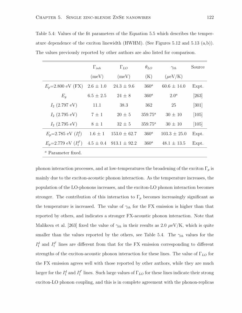
Chapter 5. Single zinc-blende ZnSe nanowires 122
Table 5.4: Values of the fit parameters of the Equation 5.5 which describes the temper-
ature dependence of the exciton linewidth (HWHM). (See Figures 5.12 and 5.13 (a,b)).
The values previously reported by other authors are also listed for comparison.
Γinh ΓLO θLO γth Source
(meV) (meV) (K) (µeV/K)
Ep=2.800 eV (FX) 2.6 ± 1.0 24.3 ± 9.6 360a 60.6 ± 14.0 Expt.
Eg 6.5 ± 2.5 24 ± 8 360a 2.0a [263]
I2 (2.797 eV) 11.1 38.3 362 25 [301]
I2 (2.795 eV) 7 ± 1 20 ± 5 359.75a 30 ± 10 [105]
I2 (2.795 eV) 8 ± 1 32 ± 5 359.75a 30 ± 10 [105]
Ep=2.785 eV (Id1 ) 1.6 ± 1 153.0 ± 62.7 360a 103.3 ± 25.0 Expt.
Ep=2.779 eV (Id′
1 ) 4.5 ± 0.4 913.1 ± 92.2 360a 48.1 ± 13.5 Expt.
a Parameter fixed.
phonon interaction processes, and at low-temperatures the broadening of the exciton Γp is
mainly due to the exciton-acoustic phonon interaction. As the temperature increases, the
population of the LO-phonons increases, and the exciton-LO phonon interaction becomes
stronger. The contribution of this interaction to Γp becomes increasingly significant as
the temperature is increased. The value of γth for the FX emission is higher than that
reported by others, and indicates a stronger FX-acoustic phonon interaction. Note that
Malikova et al. [263] fixed the value of γth in their results as 2.0 µeV/K, which is quite
smaller than the values reported by the others, see Table 5.4. The γth values for the
Id1 and Id′
1 lines are different from that for the FX emission corresponding to different
strengths of the exciton-acoustic phonon interaction for these lines. The value of ΓLO for
the FX emission agrees well with those reported by other authors, while they are much
larger for the Id1 and Id′
1 lines. Such large values of ΓLO for these lines indicate their strong
exciton-LO phonon coupling, and this is in complete agreement with the phonon-replicas

Chapter 5. Single zinc-blende ZnSe nanowires 123
0 2 0 4 0 6 0 8 0 1 0 0 1 2 002468
1 01 21 41 61 82 02 2
( b )( a )
HWHM
(meV
)
T e m p e r a t u r e ( K )
Z B - N W - 3 H W H M - E x p t . E p = 2 . 7 8 5 e V
F i t
0 2 0 4 0 6 0 8 0
Z B - N W - 3 H W H M - E x p t . E p = 2 . 7 8 0 e V
F i t
T e m p e r a t u r e ( K )
Figure 5.13: Change in HWHM for the (a) Id1 and (b) Id′
1 lines with temperature (for
ZB-NW-3). The solid lines are fits to the Equation 5.5.
up to 3rd order observed in the LTPL spectrum from ZB-NW-3, for both Id1 and Id′
1 lines.
The thermal quenching of the IPL is described by a relation of the form [302]:
IPL(T ) =IPL(0)
1 + C exp (−Ea/kBT )(5.6)
for quenching that involves one mechanism (or one-step process), where Ea is the ac-
tivation energy of the mechanism and C is a coefficient. For thermal quenching of the
recombination lines involving two mechanisms (or two-step process), the equation that
represents the temperature dependence of IPL is modified to [303]
IPL(T ) =IPL(0)
1 + C1 exp (−Ea1/kBT ) + C2 exp (−Ea2/kBT )(5.7)
where Ea1 and Ea2 are the activation energies of the two mechanisms, and C1 and C2 are
coefficients. Figure 5.14 shows the change in IPL for the FX emission with inverse tem-
perature. The dashed and the solid lines are fits to Equations 5.6 and 5.7, respectively.
The fit to a one-step process gives an Ea of 24 meV, which is close to the exciton binding

Chapter 5. Single zinc-blende ZnSe nanowires 124
5 1 0 1 5 2 0 2 5
Integ
rated
PL In
tensity
(I PL, a
rb. un
its)
1 0 0 0 / T ( K - 1 )
Z B - N W - 3 I P L - E x p t . E p = 2 . 8 0 0 e V
F i t t o t w o - s t e p p r o c e s s E a 1 = 2 0 m e V , E a 2 = 1 3 6 m e V
F i t t o o n e - s t e p p r o c e s s E a = 2 4 m e V
Figure 5.14: Change in integrated PL intensity (IPL) for the FX emission (Ep=2.800 eV)
with temperature (for ZB-NW-3). The dashed and solid lines are fits to the Equations 5.6
and 5.7, respectively. Note the log scale for IPL.
energy (of the free excitons) in ZnSe (EFX=21 meV [252]). The fit to a two-step process
however is better, and yields Ea1 and Ea2 of 20 meV and 136 meV, respectively. The Ea1
of 20 meV is close to the exciton binding energy in ZnSe, while the origin of the second
mechanism (Ea2=136 meV) is uncertain. Zhang et al. [106] observed a similar quenching
mechanism with Ea=136 meV for the IPL of the exciton emission lines in Ag-doped ZnSe
NWs. They did not specify the nature of this mechanism however. It is suggested that
this process may correspond to a non-radiative recombination mechanism, which could be
a result of the surface recombination in NWs. However, this needs further investigation.
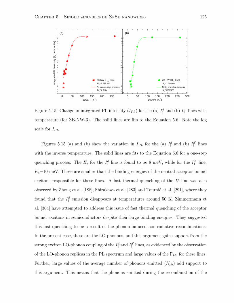
Chapter 5. Single zinc-blende ZnSe nanowires 125
0 5 0 1 0 0 1 5 0 2 0 0 2 5 0
( b )
Integ
rated
PL In
tensity
(I PL, a
rb. un
its)
1 0 0 0 / T ( K - 1 )
Z B - N W - 3 I P L - E x p t . E p = 2 . 7 8 5 e V
F i t t o o n e - s t e p p r o c e s s E a = 8 m e V
( a )
0 5 0 1 0 0 1 5 0 2 0 0 2 5 0 3 0 0
Z B - N W - 3 I P L - E x p t . E p = 2 . 7 8 0 e V
F i t t o o n e - s t e p p r o c e s s E a = 1 0 m e V
1 0 0 0 / T ( K - 1 )
Figure 5.15: Change in integrated PL intensity (IPL) for the (a) Id1 and (b) Id′
1 lines with
temperature (for ZB-NW-3). The solid lines are fits to the Equation 5.6. Note the log
scale for IPL.
Figures 5.15 (a) and (b) show the variation in IPL for the (a) Id1 and (b) Id′
1 lines
with the inverse temperature. The solid lines are fits to the Equation 5.6 for a one-step
quenching process. The Ea for the Id1 line is found to be 8 meV, while for the Id′
1 line,
Ea=10 meV. These are smaller than the binding energies of the neutral acceptor bound
excitons responsible for these lines. A fast thermal quenching of the Id1 line was also
observed by Zhong et al. [188], Shirakawa et al. [283] and Tournie et al. [291], where they
found that the Id1 emission disappears at temperatures around 50 K. Zimmermann et
al. [304] have attempted to address this issue of fast thermal quenching of the acceptor
bound excitons in semiconductors despite their large binding energies. They suggested
this fast quenching to be a result of the phonon-induced non-radiative recombinations.
In the present case, these are the LO-phonons, and this argument gains support from the
strong exciton LO-phonon coupling of the Id1 and Id′
1 lines, as evidenced by the observation
of the LO-phonon replicas in the PL spectrum and large values of the ΓLO for these lines.
Further, large values of the average number of phonons emitted (Nph) add support to
this argument. This means that the phonons emitted during the recombination of the

Chapter 5. Single zinc-blende ZnSe nanowires 126
acceptor bound excitons (which are known for their strong LO-phonon coupling) are
the cause of their faster disappearance as the temperature is increased compared to the
donor-bound excitons, despite their larger binding energies than those of the donor bound
excitons.
5.2.4 Dependence of LTPL on Iexc
LTPL from ZB-NW-1 was measured as a function of the Iexc. Figure 5.16 shows the
change in LTPL as Iexc is increased from 0.32 W/cm2 to 236.8 W/cm2. As can be seen
from Figure 5.16, the FX emission at 2.800 eV is red-shifted to 2.797 eV at the highest
Iexc. This is due to the laser heating of the ZB-NW-1. As the Iexc is increased, it becomes
more difficult to dissipate heat owing to the small volume of the NWs and lack of a good
thermal contact with the TEM grid. Bao et al. [133] observed much larger red-shifts
in PL from single InP NWs at increasing Iexc which they considered to be caused by
the laser heating. It should be noted that large red-shifts seen by Bao et al. [133] were
due to the very high Iexc they used. As the temperature of the ZB-NW-1 increases due
to the laser heating, the band gap and the energy positions of different lines also red-
shift. The analysis described in Chapter 4 using the dependence of PL on Iexc cannot
accurately describe the recombination mechanisms in this case. This is however not a
hindrance in the interpretation of the recombination lines because the dependence of PL
on temperature was useful in obtaining this information.
5.3 Conclusions
In this chapter, the results were presented on the optical characterization of single ZB
ZnSe NWs using LTPL. The structural characterization performed using TEM, HR-TEM
and SAD confirmed the single crystalline ZB microstructure of the same ZB NWs that
were studied using LTPL. The optical response was found to be dominated by emissions

Chapter 5. Single zinc-blende ZnSe nanowires 127
2 . 6 5 2 . 7 0 2 . 7 5 2 . 8 0 2 . 8 5
Z B - N W - 1PL
Inten
sity (a
rb. un
its)
E n e r g y ( e V )
7 4 0 P 0
6 0 0 P 0
4 0 0 P 03 0 0 P 02 0 0 P 0
1 0 0 P 0
4 0 P 0
2 0 P 0
1 0 P 0
4 P 0
2 P 0
P 0
P 0 = 0 . 3 2 W / c m 2
T e m p . = 3 . 5 K
Figure 5.16: Iexc-dependent LTPL spectra from ZB-NW-1. All spectra were acquired at
a constant temperature (3.9 K), are normalized to unity and displayed offset for clarity.
Chapter 5. Single zinc-blende ZnSe nanowires 128
related to the native point defects. No evidence was found of the role of unintentional
impurities in the optical properties of ZB NWs. The recombination lines at 2.785 eV
and 2.780 were assigned to the neutral acceptor bound excitons related to VZn and (VZn-
complex), respectively. Another recombination line at 2.800 eV was related to the free
excitons (FX). The binding energies of the excitons related to the Id1 and Id′
1 were found to
be 15 meV and 20 meV, respectively. The ionization energies of the acceptors responsible
for these lines were 150 meV and 200 meV, respectively. The Id1 and Id′
1 lines were
accompanied by LO-phonon replicas up to 3 orders. The average number of emitted
phonons was found to be 0.53 < Nph < 0.7 for the Id1 line, and 0.25 < Nph < 0.42 for the
Id′
1 line. There have been no reports thus far of the Id1 and Id′
1 lines and their phonon-
replicas in ZnSe NWs. Linewidths of 1.5 meV for the Id1 line were observed. These are the
narrowest linewidths reported so far on ZnSe NWs. The optical response was compared
for the single ZB NWs and a bundle of ZB NWs. For a bundle of NWs, the peak positions
of the recombination lines are similar to those from single NWs. The Y-line emission
related to structural defects was not detected. This confirms that the Y-line does not
originate from single-crystalline NWs, but rather from the polycrystalline undergrowth
on the sample. Further, the linewidths in the case of bundle of NWs were found to be
larger than in single NWs. This is related to the effects of ensemble broadening. The
linewidths exhibited by different NWs for similar conditions of acquisition of PL spectrum
were found to be slightly different, and the ensemble broadening could also be limited by
the NW which shows the largest linewidths.
The PL from single NWs was studied as a function of temperature. The temperature
dependence of the FX emission peak energy confirmed its assignment to the free exci-
tons. The high-temperature limit of the temperature gradient dEg/dT was determined
and found to be in excellent agreement with the reported values on bulk ZnSe. The
temperature dependence of the Id1 and Id′
1 lines was used to determine the parameters of
the Bose-Einstein type expression of the temperature dependence of the band gap. The
Chapter 5. Single zinc-blende ZnSe nanowires 129
dependence of HWHM for the FX emission, and Id1 and Id′
1 lines revealed the small con-
tribution of the inhomogeneous broadening to the linewidths. A strong exciton-acoustic
phonon and exciton-LO phonon coupling was found, which is consistent with the obser-
vation of LO-phonon replicas and the large average number of emitted phonons. The
integrated PL intensity of the FX emission line was found to be quenched with temper-
ature by two mechanisms. The first mechanism with an activation energy of 20 meV is
related to the dissociation of free excitons, while the other with an activation energy of
136 meV could be due to non-radiative recombination related to surface recombination.
The Id1 and Id′
1 lines were quenched with temperature with activation energies smaller
than their binding energies. These are proposed to be due to non-radiative recombination
induced by scattering of excitons with LO-phonons simultaneously emitted.
Chapter 6
Single wurtzite ZnSe nanowires
6.1 Introduction
It was mentioned in Chapter 1 that for bulk ZnSe, the WZ crystal structure is meta-
stable and is therefore difficult to obtain. This explains the availability of a vast amount
of literature on luminescence characterization of ZnSe single crystals and thin films in
the stable ZB phase, but only a few reports are available on the same for WZ bulk ZnSe
single crystals. However, unlike the bulk case, ZnSe NWs can be obtained in the WZ
crystal structure. Although the number of reports on ZB NWs still exceed those on
WZ NWs, there is a clear evidence that ZnSe NWs can also crystallize in the WZ crystal
structure. Existing reports available on WZ NWs have focused on describing their growth
and structural properties, while their optical characterization has not been adequately
described. LTPL from WZ NWs has been reported by a few authors, but these were
performed on an array of NWs which also included ZB NWs. These were discussed in
greater detail in Chapter 2. The optical response of ZB NWs was unambiguously related
to their single crystalline microstructure, and these results were presented in Chapter 5.
It is of particular importance to note that applying a similar strategy is crucial for the
case of WZ NWs, because optical transitions in WZ ZnSe have not been studied in
130
Chapter 6. Single wurtzite ZnSe nanowires 131
detail previously. The work by Liang and Yoffe [305] several decades ago is still the only
authoritative report on luminescence characterization of WZ ZnSe.
This chapter presents the results on the optical response from individual WZ NWs
with their crystal structure determined using TEM, HR-TEM and SAD, and is organ-
ised as follows. First, the results on the structural and optical characterization for an
individual WZ NW (labelled as WZ-NW-1) are presented. The origin of recombination
lines in the LTPL spectrum from WZ-NW-1 is discussed in detail with reference to the
works by Liang and Yoffe [305] and on ZB NWs. Results on luminescence characteri-
zation of another single WZ NW (labelled as WZ-NW-2) are presented thereafter. PL
from WZ-NW-1 was also studied as a function of temperature and Iexc, which are then
described. Quantitative information is extracted from the dependence of PL on temper-
ature, using the models that were used earlier in Chapter 5, and described in more detail
in Appendix C.2.2.
6.2 Results and Discussion
6.2.1 Characterization of single WZ nanowires
Six individual WZ NWs were characterized by both optical and structural characteriza-
tion techniques, and all of them were selected from the same as-grown sample. For the
determination of the crystal structure, similar to the case of ZB NWs, HR-TEM micro-
graphs were taken at several locations along the length of the NWs. The SAD patterns
were also taken at multiple locations along the length of the NWs to arrive at a conclusion
about the crystal structure. Unlike the case of ZB NWs, where most NWs were defect-
free and single-crystalline, a fraction of the WZ NWs contained stacking faults. These
are not included in the results here. In the following, results from structural characteri-
zation are presented for a single-crystalline individual WZ NW (labelled as WZ-NW-1),
and from LTPL characterization on WZ-NW-1 and another individual WZ NW (labelled
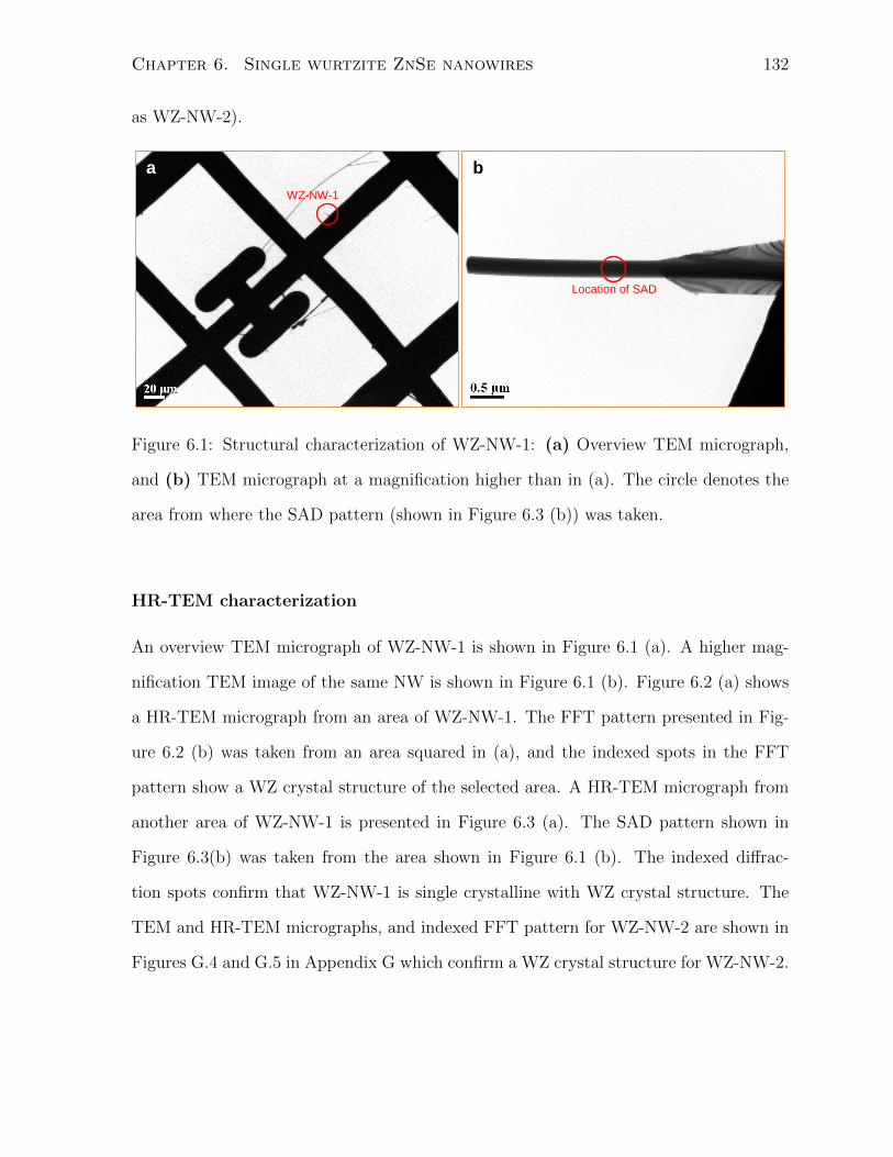
Chapter 6. Single wurtzite ZnSe nanowires 132
as WZ-NW-2).
a b
WZ-NW-1
Location of SAD
Figure 6.1: Structural characterization of WZ-NW-1: (a) Overview TEM micrograph,
and (b) TEM micrograph at a magnification higher than in (a). The circle denotes the
area from where the SAD pattern (shown in Figure 6.3 (b)) was taken.
HR-TEM characterization
An overview TEM micrograph of WZ-NW-1 is shown in Figure 6.1 (a). A higher mag-
nification TEM image of the same NW is shown in Figure 6.1 (b). Figure 6.2 (a) shows
a HR-TEM micrograph from an area of WZ-NW-1. The FFT pattern presented in Fig-
ure 6.2 (b) was taken from an area squared in (a), and the indexed spots in the FFT
pattern show a WZ crystal structure of the selected area. A HR-TEM micrograph from
another area of WZ-NW-1 is presented in Figure 6.3 (a). The SAD pattern shown in
Figure 6.3(b) was taken from the area shown in Figure 6.1 (b). The indexed diffrac-
tion spots confirm that WZ-NW-1 is single crystalline with WZ crystal structure. The
TEM and HR-TEM micrographs, and indexed FFT pattern for WZ-NW-2 are shown in
Figures G.4 and G.5 in Appendix G which confirm a WZ crystal structure for WZ-NW-2.

Chapter 6. Single wurtzite ZnSe nanowires 133
a b
1102
1101
1101
1102
0002
00021100
1102
1101
1101
1102
1100
Figure 6.2: (a) HR-TEM micrograph from an area of WZ-NW-1, (b) Indexed FFT pattern
taken from the area squared (in red) in (a). The indexed spots correspond to a WZ crystal
structure. The viewing direction for (a) and (b) is 〈1100〉.
a b
11021101
1101
1102
0002
0002
1100
1102
1101
11011102
1100
Figure 6.3: (a) HR-TEM micrograph from another area, and (b) SAD pattern acquired
from a larger area (shown in Figure 6.1(b)) of WZ-NW-1 . The indexed spots correspond
to a WZ crystal structure. The viewing direction for (a) and (b) is 〈1100〉.

Chapter 6. Single wurtzite ZnSe nanowires 134
Low-temperature PL spectra
Figure 6.4 shows the excitonic region of the LTPL spectrum (3.8 K) from WZ-NW-
1 acquired under the conditions of high throughput. The LTPL spectrum was fit to
individual emission peaks using Lorentzians as shown. The LTPL spectrum from WZ-
NW-1 is more complex than those from ZB NWs (in Chapter 5). This means that the
number of emission peaks is larger in the LTPL from WZ-NW-1, and their interpretation
more difficult. In the case of ZB NWs, the identification of recombination lines was
facilitated by the existing literature on LTPL from ZnSe single crystals and thin films.
This is however not the case for WZ NWs, since there exist only a few reports on LTPL
from WZ ZnSe (strictly speaking just one by Liang and Yoffe [305]). The identification of
recombination lines in the case of WZ-NW-1 will be discussed in terms of the identification
proposed by Liang and Yoffe [305], and by reference to the identification described for
ZB NWs.
In their work on LTPL from WZ ZnSe crystals, Liang and Yoffe [305] observed several
peaks which they related to the free and bound excitons in WZ ZnSe and their satellite
peaks (replicas) due to the simultaneous emission of acoustic and optical phonons. They
gave the energies of these phonons, as listed in the Table 6.1. However, no attempts
were made by them to identify the recombination centres responsible for these lines.
In particular, they observed peaks related to excitons bound to neutral donors, ionized
acceptors and neutral acceptors, which they labelled as I1, I2, and I3, respectively. Note,
that these labels are different from those used conventionally for bound exciton lines, i.e.
for excitons bound to neutral donors (I2), neutral acceptors (I1) and to ionized acceptors
(I3). Some of the peaks due to the emission of phonons were found to be overlapping for
these lines. They gave the binding energy of excitons bound to neutral acceptors (I3) as
0.0098 ± 0.0004 eV, and the ionization energy of the acceptors as EA=0.118 eV.
They also reported an important experiment, which they described only briefly. This
will soon be found to be very important in the current discussion on LTPL from WZ
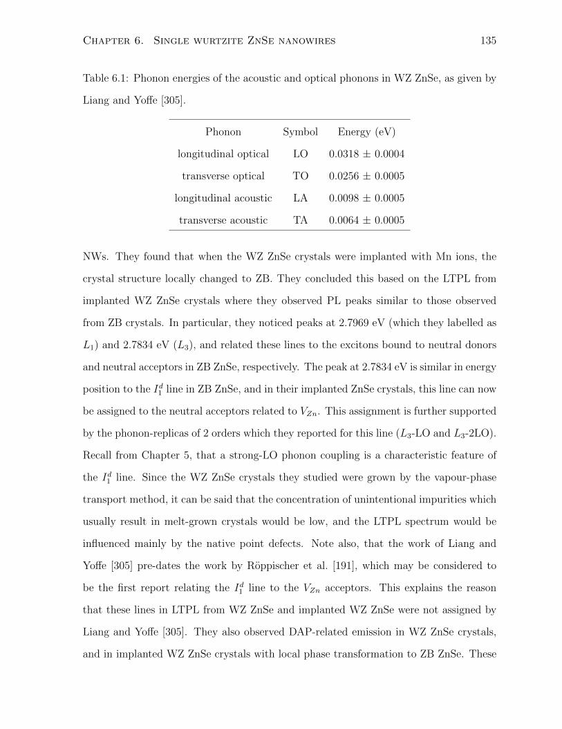
Chapter 6. Single wurtzite ZnSe nanowires 135
Table 6.1: Phonon energies of the acoustic and optical phonons in WZ ZnSe, as given by
Liang and Yoffe [305].
Phonon Symbol Energy (eV)
longitudinal optical LO 0.0318 ± 0.0004
transverse optical TO 0.0256 ± 0.0005
longitudinal acoustic LA 0.0098 ± 0.0005
transverse acoustic TA 0.0064 ± 0.0005
NWs. They found that when the WZ ZnSe crystals were implanted with Mn ions, the
crystal structure locally changed to ZB. They concluded this based on the LTPL from
implanted WZ ZnSe crystals where they observed PL peaks similar to those observed
from ZB crystals. In particular, they noticed peaks at 2.7969 eV (which they labelled as
L1) and 2.7834 eV (L3), and related these lines to the excitons bound to neutral donors
and neutral acceptors in ZB ZnSe, respectively. The peak at 2.7834 eV is similar in energy
position to the Id1 line in ZB ZnSe, and in their implanted ZnSe crystals, this line can now
be assigned to the neutral acceptors related to VZn. This assignment is further supported
by the phonon-replicas of 2 orders which they reported for this line (L3-LO and L3-2LO).
Recall from Chapter 5, that a strong-LO phonon coupling is a characteristic feature of
the Id1 line. Since the WZ ZnSe crystals they studied were grown by the vapour-phase
transport method, it can be said that the concentration of unintentional impurities which
usually result in melt-grown crystals would be low, and the LTPL spectrum would be
influenced mainly by the native point defects. Note also, that the work of Liang and
Yoffe [305] pre-dates the work by Roppischer et al. [191], which may be considered to
be the first report relating the Id1 line to the VZn acceptors. This explains the reason
that these lines in LTPL from WZ ZnSe and implanted WZ ZnSe were not assigned by
Liang and Yoffe [305]. They also observed DAP-related emission in WZ ZnSe crystals,
and in implanted WZ ZnSe crystals with local phase transformation to ZB ZnSe. These

Chapter 6. Single wurtzite ZnSe nanowires 136
2 . 5 5 2 . 6 0 2 . 6 5 2 . 7 0 2 . 7 5 2 . 8 0 2 . 8 5 2 . 9 0
DAP-3
LO DAP-2
LO
DAP-1
LO
L T P L - W Z - N W - 1 I 1 l i n e I 1
d l i n e I n d i v i d u a l p e a k s S u m o f i n d i v i d u a l p e a k s
T e m p . = 3 . 8 K I e x c = 3 . 8 W / c m 2
d s l i t = 3 0 0 µmPL
Inten
sity (a
rb. un
its)
E n e r g y ( e V )
I 1d -1LO
I 1-1LODA
P
5 . 8 m e V
Figure 6.4: Excitonic region of the LTPL spectrum (3.8 K) from WZ-NW-1 acquired
under the conditions of high-throughput. (Iexc and dslit are as indicated). The inset
shows a confocal PL image of WZ-NW-1 under laser excitation with an average Iexc=12.7
W/cm2. The LTPL spectrum was fit to individual emission peaks using Lorentzians as
shown.
DAP-related transitions were accompanied by LO-phonon replicas in both cases.
In the LTPL spectrum from WZ-NW-1 (shown in Figure 6.4), two dominant lines are
observed at 2.841 eV and 2.833 eV. These are also of approximately the same strengths
(when comparing the peak heights). The binding energy of the excitons can be found
using EBX = Eg −EFX −Ep, where EBX is the binding energy of the donor or acceptor
bound excitons. In the case of WZ ZnSe, Eg and EFX are 2.874 eV [238] and 22 meV [238],
respectively. These give for the line with Ep=2.841 eV, EBX=11 meV, and for the line

Chapter 6. Single wurtzite ZnSe nanowires 137
with Ep=2.833 eV, EBX=19 meV. The EBX of the line at 2.841 eV is similar to that
reported by Liang and Yoffe [305] for the acceptor bound excitons line (9.8 meV). This
line at 2.841 eV can therefore be related to acceptor bound excitons. According to the
empirical rule of Halsted and Aven [253], the ionization energy of the acceptor is 110
meV, which is similar to value reported by Liang and Yoffe [305] mentioned earlier (118
meV). The other line at 2.833 eV can be related to a deep acceptor, whose ionization
energy is 190 meV. Since in their Mn-ion implanted WZ ZnSe samples, a line similar to
the Id1 line was observed, the neutral acceptor responsible the L3 line (their notation)
can be related to VZn. The observation of these two lines in the LTPL from WZ-NW-1
is similar to the case of ZB NWs where two dominating lines (Id1 and Id′
1 ) were observed.
Id1 line was assigned to the excitons bound to deep neutral acceptors related to VZn,
whereas Id′
1 was ascribed to neutral acceptors related to the VZn-complex. In the case
of WZ-NW-1, therefore, VZn act as shallow acceptors and are responsible for the line at
2.841 eV (labelled in the present case as I1). The other line at 2.833 eV, with reference to
the ZB NWs, can be ascribed to the VZn-complex acceptors which act as deep acceptors.
This line is labelled as the Id1 line. These lines and their 1st LO-phonon replica are
indicated on the Figure 6.4. The other lines can be assigned to the phonon-replicas of
the I1 and Id1 lines, similar to the assignment proposed by Liang and Yoffe [305]. The
energy positions of these lines and suggested assignments based on the present work are
listed in Table 6.2. The energy positions and suggested assignments for the lines given by
Liang and Yoffe [305] are also listed in Table 6.2. Only the lines common to the present
work, and I1 and I2 lines (their notation) are listed. Note that there are no common
assignments except for the case of the I1 line at 2.841 eV. This is the first time since the
work of Liang and Yoffe [305] that a recombination scheme has been proposed for the
optical transitions in WZ ZnSe.
The peak with Ep=2.741 eV is assigned to the DAP-related transition, similar to the
previous assignment by Liang and Yoffe [305] for their PL peak at 2.7384 eV. The peaks
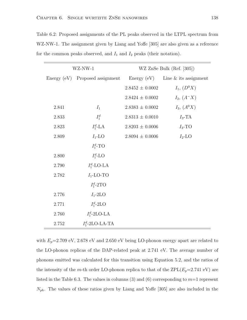
Chapter 6. Single wurtzite ZnSe nanowires 138
Table 6.2: Proposed assignments of the PL peaks observed in the LTPL spectrum from
WZ-NW-1. The assignment given by Liang and Yoffe [305] are also given as a reference
for the common peaks observed, and I1 and I2 peaks (their notation).
WZ-NW-1 WZ ZnSe Bulk (Ref. [305])
Energy (eV) Proposed assignment Energy (eV) Line & its assignment
2.8452 ± 0.0002 I1, (D0X)
2.8424 ± 0.0002 I2, (A−X)
2.841 I1 2.8383 ± 0.0002 I3, (A0X)
2.833 Id1 2.8313 ± 0.0010 I3-TA
2.823 Id1 -LA 2.8203 ± 0.0006 I3-TO
2.809 I1-LO 2.8094 ± 0.0006 I2-LO
Id1 -TO
2.800 Id1 -LO
2.790 Id1 -LO-LA
2.782 I1-LO-TO
Id1 -2TO
2.776 I1-2LO
2.771 Id1 -2LO
2.760 Id1 -2LO-LA
2.752 Id1 -2LO-LA-TA
with Ep=2.709 eV, 2.678 eV and 2.650 eV being LO-phonon energy apart are related to
the LO-phonon replicas of the DAP-related peak at 2.741 eV. The average number of
phonons emitted was calculated for this transition using Equation 5.2, and the ratios of
the intensity of the m-th order LO-phonon replica to that of the ZPL(Ep=2.741 eV) are
listed in the Table 6.3. The values in columns (3) and (6) corresponding to m=1 represent
Nph. The values of these ratios given by Liang and Yoffe [305] are also included in the
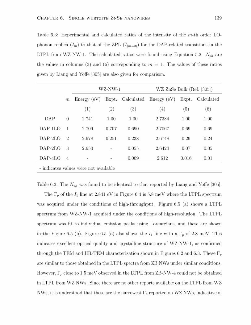
Chapter 6. Single wurtzite ZnSe nanowires 139
Table 6.3: Experimental and calculated ratios of the intensity of the m-th order LO-
phonon replica (Im) to that of the ZPL (I(m=0)) for the DAP-related transitions in the
LTPL from WZ-NW-1. The calculated ratios were found using Equation 5.2. Nph are
the values in columns (3) and (6) corresponding to m = 1. The values of these ratios
given by Liang and Yoffe [305] are also given for comparison.
WZ-NW-1 WZ ZnSe Bulk (Ref. [305])
m Energy (eV) Expt. Calculated Energy (eV) Expt. Calculated
(1) (2) (3) (4) (5) (6)
DAP 0 2.741 1.00 1.00 2.7384 1.00 1.00
DAP-1LO 1 2.709 0.707 0.690 2.7067 0.69 0.69
DAP-2LO 2 2.678 0.251 0.238 2.6748 0.29 0.24
DAP-2LO 3 2.650 - 0.055 2.6424 0.07 0.05
DAP-4LO 4 - - 0.009 2.612 0.016 0.01
- indicates values were not available
Table 6.3. The Nph was found to be identical to that reported by Liang and Yoffe [305].
The Γp of the I1 line at 2.841 eV in Figure 6.4 is 5.8 meV where the LTPL spectrum
was acquired under the conditions of high-throughput. Figure 6.5 (a) shows a LTPL
spectrum from WZ-NW-1 acquired under the conditions of high-resolution. The LTPL
spectrum was fit to individual emission peaks using Lorentzians, and these are shown
in the Figure 6.5 (b). Figure 6.5 (a) also shows the I1 line with a Γp of 2.8 meV. This
indicates excellent optical quality and crystalline structure of WZ-NW-1, as confirmed
through the TEM and HR-TEM characterization shown in Figures 6.2 and 6.3. These Γp
are similar to those obtained in the LTPL spectra from ZB NWs under similar conditions.
However, Γp close to 1.5 meV observed in the LTPL from ZB-NW-4 could not be obtained
in LTPL from WZ NWs. Since there are no other reports available on the LTPL from WZ
NWs, it is understood that these are the narrowest Γp reported on WZ NWs, indicative of
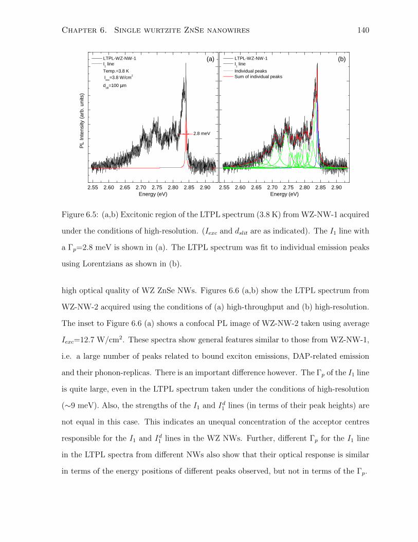
Chapter 6. Single wurtzite ZnSe nanowires 140
2 . 5 5 2 . 6 0 2 . 6 5 2 . 7 0 2 . 7 5 2 . 8 0 2 . 8 5 2 . 9 0
PL In
tensity
(arb.
units)
E n e r g y ( e V )
L T P L - W Z - N W - 1 I 1 l i n e
T e m p . = 3 . 8 K I e x c = 3 . 8 W / c m 2
d s l i t = 1 0 0 µm
2 . 8 m e V
2 . 5 5 2 . 6 0 2 . 6 5 2 . 7 0 2 . 7 5 2 . 8 0 2 . 8 5 2 . 9 0
( b ) L T P L - W Z - N W - 1 I 1 l i n e I n d i v i d u a l p e a k s S u m o f i n d i v i d u a l p e a k s
E n e r g y ( e V )
( a )
Figure 6.5: (a,b) Excitonic region of the LTPL spectrum (3.8 K) from WZ-NW-1 acquired
under the conditions of high-resolution. (Iexc and dslit are as indicated). The I1 line with
a Γp=2.8 meV is shown in (a). The LTPL spectrum was fit to individual emission peaks
using Lorentzians as shown in (b).
high optical quality of WZ ZnSe NWs. Figures 6.6 (a,b) show the LTPL spectrum from
WZ-NW-2 acquired using the conditions of (a) high-throughput and (b) high-resolution.
The inset to Figure 6.6 (a) shows a confocal PL image of WZ-NW-2 taken using average
Iexc=12.7 W/cm2. These spectra show general features similar to those from WZ-NW-1,
i.e. a large number of peaks related to bound exciton emissions, DAP-related emission
and their phonon-replicas. There is an important difference however. The Γp of the I1 line
is quite large, even in the LTPL spectrum taken under the conditions of high-resolution
(∼9 meV). Also, the strengths of the I1 and Id1 lines (in terms of their peak heights) are
not equal in this case. This indicates an unequal concentration of the acceptor centres
responsible for the I1 and Id1 lines in the WZ NWs. Further, different Γp for the I1 line
in the LTPL spectra from different NWs also show that their optical response is similar
in terms of the energy positions of different peaks observed, but not in terms of the Γp.

Chapter 6. Single wurtzite ZnSe nanowires 141
2 . 5 5 2 . 6 0 2 . 6 5 2 . 7 0 2 . 7 5 2 . 8 0 2 . 8 5 2 . 9 0 2 . 9 5
( b )
PL In
tensity
(arb.
units)
E n e r g y ( e V )
L T P L - W Z - N W - 2 I 1 l i n e I n d i v i d u a l p e a k s S u m o f i n d i v i d u a l p e a k s
T e m p . = 4 . 0 K I e x c = 3 1 . 8 W / c m 2
d s l i t = 5 0 0 µm
1 0 m e V
( a )
2 . 5 5 2 . 6 0 2 . 6 5 2 . 7 0 2 . 7 5 2 . 8 0 2 . 8 5 2 . 9 0
L T P L - W Z - N W - 2 I 1 l i n e I n d i v i d u a l p e a k s S u m o f i n d i v i d u a l p e a k s
T e m p . = 4 . 0 K I e x c = 3 . 2 W / c m 2
d s l i t = 1 0 0 µm
E n e r g y ( e V )
9 m e V
Figure 6.6: Excitonic region of the LTPL spectrum (4.0 K) acquired from WZ-NW-2
under the conditions of (a) high-throughput, and (b) high-resolution. (Iexc and dslit are
as indicated). The inset in (a) shows a confocal PL image of WZ-NW-2 under laser
excitation with average Iexc=12.7 W/cm2. The LTPL spectra in both cases were fit to
individual emission peaks using Lorentzians as shown.
6.2.2 Dependence of PL on temperature
PL from WZ-NW-1 was measured as a function of the sample temperature. The variation
in PL from WZ-NW-1 as the temperature is increased from 4 K to the RT is shown in
Figure 6.7. It was observed that the intensity of PL emission is quenched rapidly as the
temperature is increased, and no PL was detected at temperatures above 130 K. Further,
it can also be seen from Figure 6.7 that the excitonic (I1 and Id1 ) PL lines diminish as the
temperature is increased, while the DAP recombinations persist at higher temperatures
(up to 100 K). Figure 6.8 shows the change in energy position of the I1 line with the
temperature. It is seen that the peak energy first increases as the temperature is increased
to 40 K, and then decreases with increasing temperature. This can be understood as
follows. The excitons bound to the VZn responsible for the I1 line dissociate from the
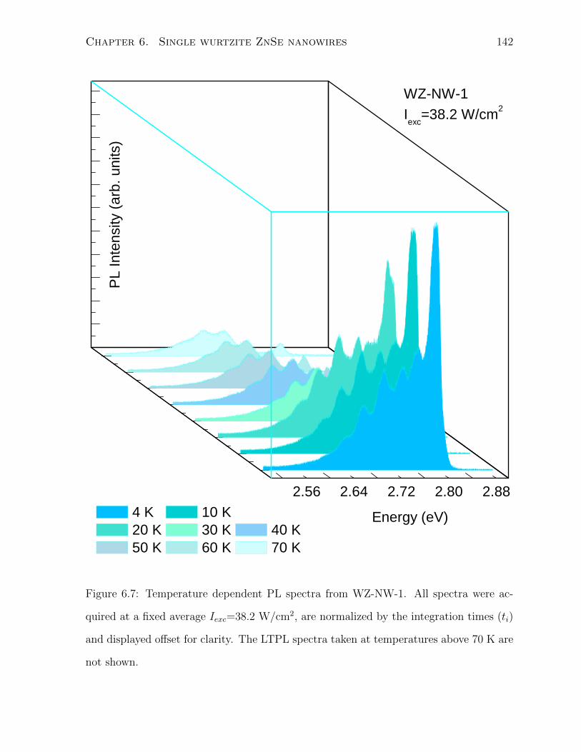
Chapter 6. Single wurtzite ZnSe nanowires 142
2 . 5 6 2 . 6 4 2 . 7 2 2 . 8 0 2 . 8 8 4 K 1 0 K 2 0 K 3 0 K 4 0 K 5 0 K 6 0 K 7 0 K
PL In
tensity
(arb.
units)
E n e r g y ( e V )
W Z - N W - 1I e x c = 3 8 . 2 W / c m 2
Figure 6.7: Temperature dependent PL spectra from WZ-NW-1. All spectra were ac-
quired at a fixed average Iexc=38.2 W/cm2, are normalized by the integration times (ti)
and displayed offset for clarity. The LTPL spectra taken at temperatures above 70 K are
not shown.

Chapter 6. Single wurtzite ZnSe nanowires 143
VZn centres, and become free excitons (FX). The energy position of the FX emission
changes as the band gap shrinks with increasing temperatures and reflects this change.
The solid and dashed lines in Figure 6.8 are fits to the Equation 5.4 (Bose-Einstein type
expression for the temperature dependence of the Eg) at temperatures above 30 K and
40 K, respectively. This means that Eg(0) in Equation 5.4 corresponds to Eg(30) and
Eg(40) for the solid and dashed lines, respectively. These are found to be 2.845 eV in both
cases. The parameters obtained from the fits are listed in Table 6.4. These parameters
have not been reported in the literature previously, so they cannot be compared with
other works. Similar to the case of the Id1 and Id′
1 lines (ZB-NW-3 in Chapter 5), a fit
of the energy positions of the I1 line at different temperatures to the Varshni’s equation
(Equation 5.3) did not converge. This can be explained by the same reasoning as given
earlier in Chapter 5.
This process of dissociation of bound excitons to free excitons is also supported by
the fit of IPL at different temperatures to the thermal quenching process involving one
mechanism, described by the Equation 5.6. Figure 6.9 shows the change in IPL with
temperature, and the solid line is a fit to the Equation 5.6. The activation energy of the
thermal quenching process was found to be 9 meV, which is in good agreement with the
binding energy of the neutral acceptor bound excitons (11 meV) related to the I1 line.
Table 6.4: Values of the fit parameters of the Bose-Einstein type expression (Equation 5.4)
which describes the temperature dependence of the direct Eg. (See Figure 6.8).
Eg(0) αB θB Source
(eV) (meV) (K)
2.845 ± 0 69.8 ± 9.2 250.4 ± 14.6 Expt.
2.845 ± 0 64.6 ± 9.6 241.0 ± 16.8 Expt.
Figure 6.10 shows the change in the Γp/2 (HWHM) of the I1 exciton emission line with
the temperature for WZ-NW-1. The change in HWHM with temperature is described

Chapter 6. Single wurtzite ZnSe nanowires 144
0 2 0 4 0 6 0 8 0 1 0 0 1 2 02 . 8 2 0
2 . 8 2 5
2 . 8 3 0
2 . 8 3 5
2 . 8 4 0
2 . 8 4 5
Energ
y (eV
)
T e m p e r a t u r e ( K )
W Z - N W - 1 - E x p t . E p = 2 . 8 4 1 e V
F i t F i t
Figure 6.8: Variation in PL peak energy of the I1 line (Ep=2.841 eV) (for WZ-NW-1) with
temperature. The solid and dashed lines are fits to the Equation 5.4 for temperatures
above 30 K and 40 K, respectively.
by the Equation 5.5, and the solid line in Figure 6.10 is a fit to this equation. The
parameters obtained from the fit are listed in Table 6.5. These parameters from the
literature cannot be listed as they have not been reported before for WZ ZnSe. These
are however listed for the Id1 line in LTPL from ZB-NW-3 for comparison. The value of
Γinh which represents the inhomogeneous broadening term is larger than for the Id1 line.
This can be understood by considering that the Γp for the WZ-NW-1 is somewhat larger
than that for the Id1 line. A large value of ΓLO indicates a strong LO-phonon coupling,
but less stronger than that for the Id1 line in ZB-NW-1. This is explained by the 2 orders
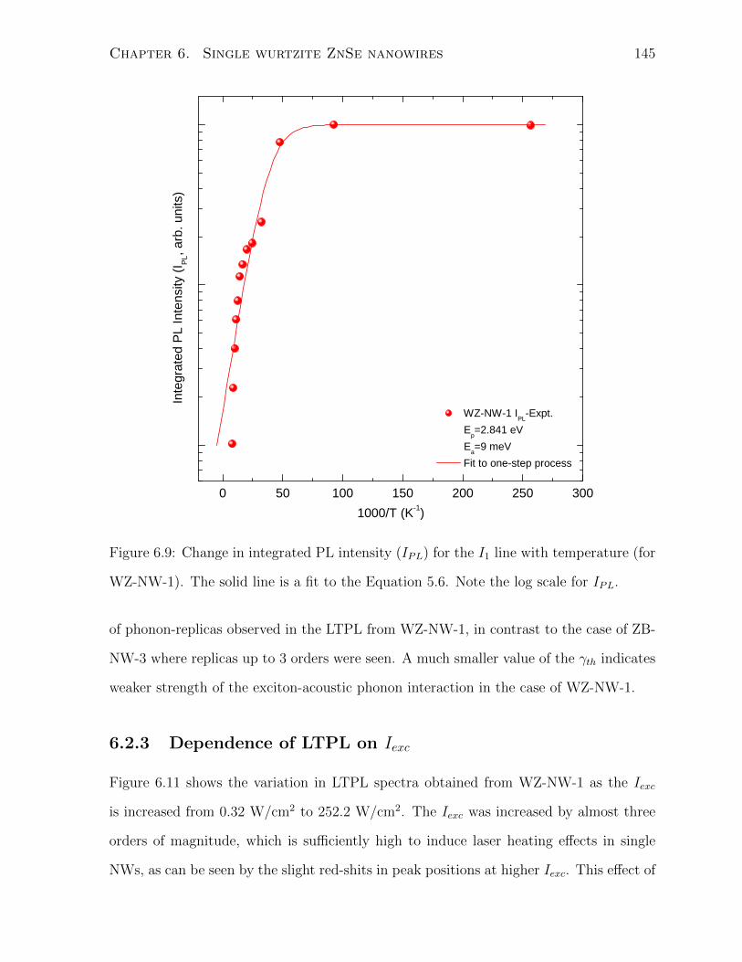
Chapter 6. Single wurtzite ZnSe nanowires 145
0 5 0 1 0 0 1 5 0 2 0 0 2 5 0 3 0 0
Integ
rated
PL In
tensity
(I PL, a
rb. un
its)
1 0 0 0 / T ( K - 1 )
W Z - N W - 1 I P L - E x p t . E p = 2 . 8 4 1 e V E a = 9 m e V
F i t t o o n e - s t e p p r o c e s s
Figure 6.9: Change in integrated PL intensity (IPL) for the I1 line with temperature (for
WZ-NW-1). The solid line is a fit to the Equation 5.6. Note the log scale for IPL.
of phonon-replicas observed in the LTPL from WZ-NW-1, in contrast to the case of ZB-
NW-3 where replicas up to 3 orders were seen. A much smaller value of the γth indicates
weaker strength of the exciton-acoustic phonon interaction in the case of WZ-NW-1.
6.2.3 Dependence of LTPL on Iexc
Figure 6.11 shows the variation in LTPL spectra obtained from WZ-NW-1 as the Iexc
is increased from 0.32 W/cm2 to 252.2 W/cm2. The Iexc was increased by almost three
orders of magnitude, which is sufficiently high to induce laser heating effects in single
NWs, as can be seen by the slight red-shits in peak positions at higher Iexc. This effect of

Chapter 6. Single wurtzite ZnSe nanowires 146
0 2 0 4 0 6 0 8 0 1 0 0 1 2 0
4
6
8
1 0
1 2
1 4
HWHM
(meV
)
T e m p e r a t u r e ( K )
W Z - N W - 1 H W H M - E x p t . E p = 2 . 8 4 1 e V
F i t
Figure 6.10: Change in HWHM for the I1 line (Ep=2.841 eV) with temperature (for
WZ-NW-1). The solid line is a fit to the Equation 5.5.
laser heating was also observed in ZB-NW-1 (discussed in Chapter 5), which precluded the
accurate determination of the quantitative information about the different recombination
mechanisms based on the dependence of PL on Iexc. However, it may be noted from
Figure 6.11 that the higher energy emission lines I1 and Id1 at 2.841 eV and 2.832 eV,
respectively, which are due to the shallow-acceptor bound excitons, continue to increase
in intensity as the Iexc is increased. The DAP-related emission peaks at 2.741 eV and
below tend to saturate at higher Iexc. This provides support to the assignment of these
peaks discussed earlier.

Chapter 6. Single wurtzite ZnSe nanowires 147
2 . 5 5 2 . 6 0 2 . 6 5 2 . 7 0 2 . 7 5 2 . 8 0 2 . 8 5 2 . 9 0
7 8 8 P 06 0 0 P 0
4 0 0 P 0
3 0 0 P 0
2 0 0 P 0
1 0 0 P 0
4 0 P 0
2 0 P 0
1 0 P 0
4 P 0
2 P 0
W Z - N W - 1P 0 = 0 . 3 2 W / c m 2
T e m p . = 3 . 8 K
P 0
PL In
tensity
(arb.
units)
E n e r g y ( e V )Figure 6.11: Iexc-dependent LTPL spectra from WZ-NW-1. All spectra were acquired at
a constant temperature (3.8 K), are normalized to unity and displayed offset for clarity.

Chapter 6. Single wurtzite ZnSe nanowires 148
Table 6.5: Values of the fit parameters of the Equation 5.5 which describes the tem-
perature dependence of the exciton linewidth (HWHM). (See Figure 6.10). The values
obtained for the Id1 line for ZB-NW-3 are also listed for comparison.
Γinh ΓLO θLO γth Source
(meV) (meV) (K) (µeV/K)
WZ-NW-1
Ep=2.841 eV (I1) 4.0 ± 0.2 110.6 ± 10.0 360a 32.7 ± 4.1 Expt.
ZB-NW-3
Ep=2.785 eV (Id1 ) 1.6 ± 1 153.0 ± 62.7 360a 103.3 ± 25.0 Expt.
a Parameter fixed.
6.3 Conclusions
Characteristics of the optical response of single WZ ZnSe NWs were presented in this
chapter in direct relation to their crystal structure. The crystal structure for NWs were
found to be WZ based on TEM, HR-TEM and SAD experiments with their single crys-
talline microstructure. The recombination centres responsible for the PL peaks in the
LTPL spectra from single WZ NWs were identified based on the work of Liang and
Yoffe [305] and by reference to the identification of PL lines for ZB NWs. The optical re-
sponse was found to be dominated by native point defects in WZ ZnSe. A recombination
line at 2.841 eV (I1) was related to the excitons bound to neutral acceptors related to
VZn, which act as deep neutral acceptors in ZB NWs. The binding energy for this exciton
was found to be 11 meV, and the ionization energy of the acceptor 110 meV. Another
recombination line at 2.833 eV (Id1 ) was related to the excitons bound to the deep neutral
acceptors related to VZn-complexes by reference to their observation in ZB NWs. The
binding energy of this exciton and the ionization energy of the acceptor were found to be
19 meV and 190 meV, respectively. Other transitions observed in the LTPL spectra from

Chapter 6. Single wurtzite ZnSe nanowires 149
WZ NWs were related to the simultaneous emission of acoustic and optical phonons, and
a recombination scheme was proposed. This is the first time since the work of Liang and
Yoffe [305] that a transition scheme has been proposed, and acceptors responsible for
binding the excitons identified. DAP-related transitions were also observed with their
LO-phonon replicas, and the average number of phonons emitted was found to be 0.69 in
agreement with the results of Liang and Yoffe [305]. The linewidths for the I1 line of 2.8
meV were obtained, which indicate excellent optical and crystalline quality of the WZ
NWs. It was also noted that such narrow linewidths have not been reported thus far on
WZ ZnSe NWs, suggestive of their high optical quality. The parameters αB and θB for the
dependence of PL peak energy on temperature were deduced from the dependence of PL
on temperature. The other parameters that were extracted include those related to the
inhomogeneous broadening of the I1 line (Γinh=4.0±0.2), strength of the exciton-acoustic
phonon (γth=32.7±4.1 µeV/K) and exciton-LO phonon (ΓLO=110.6±10.0) interactions.
The activation energy for the thermal quenching of the I1 line was found to be 9 meV in
agreement with the binding energy of the excitons responsible for the I1 lines. This con-
stitutes the first report on detailed characterization and understanding of luminescence
properties of single WZ NWs. This understanding is crucial for design of reliable and
efficient optoelectronic devices with their desired characteristics.
Chapter 7
ZnSe Nanowire Twinning
Superlattices
7.1 Introduction
The distinct properties of emerging nanoscale structures, referred to as NTSLs, based
on their unique structure was discussed in Chapter 1. Their potential in future opto-
electronic and photonic devices, and in materials engineering at the nanoscale was also
discussed therein. It was described in Chapter 2 that the electronic properties of NTSLs
are not understood yet. Further, it was also emphasized that the determination of the
electronic properties of NTSLs as a function of their twin-plane spacing (d) is hindered
by the technical difficulties involved in nanoscale mapping of the physical properties of
the NTSLs (e.g. Eg) with their structure. In this chapter, results are presented on the
extensive optical and structural characterization of individual NTSLs, organized as fol-
lows. First, a periodicity parameter is defined as being inversely proportional to d in
NTSLs, and structural characterization results of a few representative NTSLs are pre-
sented. This is followed by a description of the LTPL spectrum from an individual NTSL,
and the observation of Eg larger than that of ZB ZnSe is discussed in terms of the poly-
150

Chapter 7. ZnSe Nanowire Twinning Superlattices 151
type character of NTSLs. The dependence of LTPL on Iexc is then presented to confirm
this polytype character of NTSLs. The experimental demonstration of variation in Eg
of NTSLs is then presented with a brief description of supporting ab Initio electronic
structure calculations. This variation is expressed as a function of the periodicity pa-
rameters (related to d), and related to Eg for ZB and WZ ZnSe. The TRPL decay from
an individual NTSL is compared with that from a single homogeneous ZB NW to show
that the PL lifetimes in the two cases are similar. The dependence of PL on temperature
for an individual NTSL is then presented, and the temperature gradient dEg/dT of a
NTSL is compared with that of ZB NWs and WZ ZnSe (bulk). The activation energies
of the thermal quenching of PL emission from a NTSL are deduced from its dependence
on temperature, and the parameters related to electron-phonon coupling are obtained.
7.1.1 Periodicity parameter (γ)
As discussed in Chapter 1, the twin-planes are atomically sharp interfaces separating
the two ZB ZnSe domains rotated with respect to each other by 60◦ (or odd multi-
ples thereof). Twin-plane spacing d in NTSLs is equal to d〈111〉N , where d〈111〉 is the
inter-planar spacing in 〈111〉-ZB direction and N is the number of monolayers between
successive twin-planes. d and d〈111〉 are shown in the schematic in Figure 1.2. In order to
characterize NTSLs, a periodicity parameter γ=d〈111〉/d=1/N is defined, such that each
NTSL can be represented as NTSL(γ). All NTSLs have been labelled as NTSL-i(γ),
where index i =1-7 corresponds to the 7 NTSLs presented in this chapter. Figures 7.1
(a)-(c) show HR-TEM micrographs of three representative NTSLs with different twin-
plane spacings d (=Nd〈111〉). The three NTSLs in Figures 7.1 (a)-(c) are NTSL-1(0.100),
NTSL-2(0.077) and NTSL-3(0.059). Figure 7.1 (d) shows a normal percentile distribution
of segment widths in NTSL-3(0.059). The individual domains are 〈111〉-ZB ZnSe with
〈111〉-direction coinciding with the growth direction of NTSL. This is confirmed by the
indexed spots in power spectrum (shown in Figure 7.1 (e)) taken at the area highlighted

Chapter 7. ZnSe Nanowire Twinning Superlattices 152
in Figure 7.1 (c) of NTSL-3(0.059). Double (twin) spots in the SAD pattern are charac-
teristic of periodic twinning, and double spots seen in the SAD pattern from a larger area
of NTSL-3(0.059) (shown in Figure 7.1 (f)) further highlight the excellent periodicity of
twin-planes. The SAD pattern shows the diffraction spots corresponding to two rotated
ZB ZnSe domains, and these are shown as directions with and without a subscript T (de-
notes twinning) in Figure 7.1 (f). It is to be noted that most reported SADs from NTSLs
show streaks instead of double spots, thus indicating their compromised periodicity.
It was observed that there is a dispersion in the distribution of twin-plane spacings d
of an individual NTSL. The distribution of individual segment widths of NTSLs matches
a normal distribution which would be expected if the variation in d is random. The mean
(µ), standard error in mean (s.e.m.) (∆µ) and standard deviation (σ) of the distribution
are taken to represent d, error in d (=δd) and dispersion (∆d), respectively. The segment
widths were measured by counting the number of monolayers on HR-TEM images (for
smaller d’s), and also by measuring the widths of entire segments from TEM images (for
larger d’s) in which case they were rounded to the nearest multiple of d〈111〉. A small
value of ∆d=0.65 nm which translates to a remarkably low fluctuations of ±2 monolayers
in the normal percentile distribution of segment widths of NTSL-3(0.059) (shown in
Figure 7.1 (d)) indicates excellent periodicity of twin-planes, and compares favourably
with all previously reported growths of NTSLs [77, 104, 124, 132, 201]. Distributions of
segment widths for all NTSLs presented in this chapter are shown as histograms in Figure
7.2, and their statistical parameters described above are listed in Table 7.1. Effectively,
for small values of ∆d the NW is considered a NTSL with periodically arranged twin-
planes, while for large ∆d or large values of coefficient of variation, (COV=σ/µ) the
NW is labelled a randomly twinned NW (RTNW), where twin-planes occur at random
positions along the length of the NW with no observable periodicity. In samples studied
here, occurrence of both NTSLs and RTNWs were expectedly found and both were
characterized similarly.
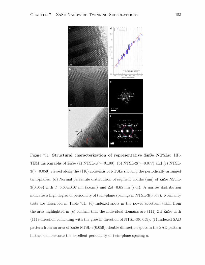
Chapter 7. ZnSe Nanowire Twinning Superlattices 153
4.0 4.5 5.0 5.5 6.0 6.5 7.0 7.5
0.01
1
10
40
70
95
99.5
Normal Probability Plot of NTSL-3 (0.059)
d = 5.635 nm d = 0.654 nm
Norm
al P
erc
entile
s
Width of segments (nm)
Percentiles
Reference Line
a
e
d
c
b
f
111
002 111
T 111 002
T
002 111
111
T
002T
<111>
111
111
220
111
002
131
131
002
111
220
222 222
131
220T
131
220
131T
220 220T
131T
111
Figure 7.1: Structural characterization of representative ZnSe NTSLs: HR-
TEM micrographs of ZnSe (a) NTSL-1(γ=0.100), (b) NTSL-2(γ=0.077) and (c) NTSL-
3(γ=0.059) viewed along the 〈110〉 zone-axis of NTSLs showing the periodically arranged
twin-planes. (d) Normal percentile distribution of segment widths (nm) of ZnSe NSTL-
3(0.059) with d=5.63±0.07 nm (s.e.m.) and ∆d=0.65 nm (s.d.). A narrow distribution
indicates a high degree of periodicity of twin-plane spacings in NTSL-3(0.059). Normality
tests are described in Table 7.1. (e) Indexed spots in the power spectrum taken from
the area highlighted in (c) confirm that the individual domains are 〈111〉-ZB ZnSe with
〈111〉-direction coinciding with the growth direction of NTSL-3(0.059). (f) Indexed SAD
pattern from an area of ZnSe NTSL-3(0.059), double diffraction spots in the SAD pattern
further demonstrate the excellent periodicity of twin-plane spacing d.

Chapter 7. ZnSe Nanowire Twinning Superlattices 154
0 5 1 0 1 5 2 0 2 5 3 0 3 5 4 00
5
1 0
1 5
2 0
2 5
3 0
3 5
4 0 N T S L - 1 ( 0 . 1 0 0 ) N T S L - 2 ( 0 . 0 7 7 ) N T S L - 3 ( 0 . 0 5 9 ) N T S L - 4 ( 0 . 0 1 2 ) N T S L - 5 ( 0 . 0 1 9 )
No. o
f cou
nts
W i d t h o f s e g m e n t s ( n m )
Figure 7.2: Histograms representing the distributions of segment widths (nm) for NTSLs
1-5. The dashed curves are normal approximations to the distributions. The correspond-
ing twin-plane spacing d, error in d (δd) (s.e.m.) and dispersion in twin-plane spacing
∆d (s.d.) are listed in Table 7.1 along with the results of the normality tests.
Figure 7.3 (a) shows LTPL spectrum from NTSL-4(0.012), whose HR-TEM micro-
graph is shown in Figure 7.3 (b). As discussed previously in Chapter 1, the LTPL
spectrum from ZnSe, similar to most II-VI compound semiconductors, is usually com-
plex and dominated by emissions related to free and bound excitons, free-to-bound and
donor-acceptor pair (DAP) related transitions, as well as their phonon replicas [7]. The
accepted energy band gap of ZB ZnSe Eg,ZB is 2.822 eV (± 2-3 meV) [7], and associ-
ated LTPL peaks are well documented [7]. LTPL spectrum from a single ZB NW was
experimentally obtained (Chapter 5). The LTPL spectrum in Figure 7.3 (a) from NTSL-
4(0.012) shows features similar to those observed in LTPL from a ZB-NW-1, with free
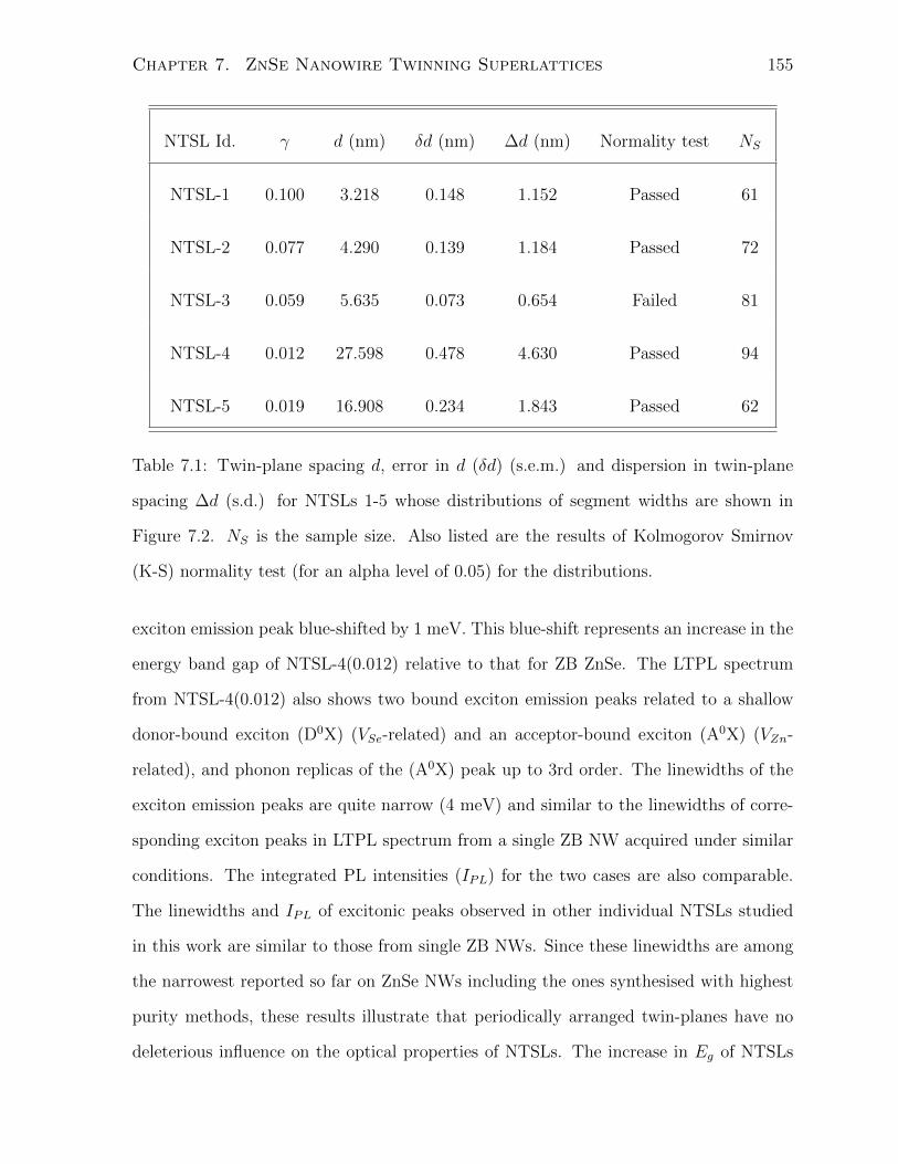
Chapter 7. ZnSe Nanowire Twinning Superlattices 155
NTSL Id. γ d (nm) δd (nm) ∆d (nm) Normality test NS
NTSL-1 0.100 3.218 0.148 1.152 Passed 61
NTSL-2 0.077 4.290 0.139 1.184 Passed 72
NTSL-3 0.059 5.635 0.073 0.654 Failed 81
NTSL-4 0.012 27.598 0.478 4.630 Passed 94
NTSL-5 0.019 16.908 0.234 1.843 Passed 62
Table 7.1: Twin-plane spacing d, error in d (δd) (s.e.m.) and dispersion in twin-plane
spacing ∆d (s.d.) for NTSLs 1-5 whose distributions of segment widths are shown in
Figure 7.2. NS is the sample size. Also listed are the results of Kolmogorov Smirnov
(K-S) normality test (for an alpha level of 0.05) for the distributions.
exciton emission peak blue-shifted by 1 meV. This blue-shift represents an increase in the
energy band gap of NTSL-4(0.012) relative to that for ZB ZnSe. The LTPL spectrum
from NTSL-4(0.012) also shows two bound exciton emission peaks related to a shallow
donor-bound exciton (D0X) (VSe-related) and an acceptor-bound exciton (A0X) (VZn-
related), and phonon replicas of the (A0X) peak up to 3rd order. The linewidths of the
exciton emission peaks are quite narrow (4 meV) and similar to the linewidths of corre-
sponding exciton peaks in LTPL spectrum from a single ZB NW acquired under similar
conditions. The integrated PL intensities (IPL) for the two cases are also comparable.
The linewidths and IPL of excitonic peaks observed in other individual NTSLs studied
in this work are similar to those from single ZB NWs. Since these linewidths are among
the narrowest reported so far on ZnSe NWs including the ones synthesised with highest
purity methods, these results illustrate that periodically arranged twin-planes have no
deleterious influence on the optical properties of NTSLs. The increase in Eg of NTSLs
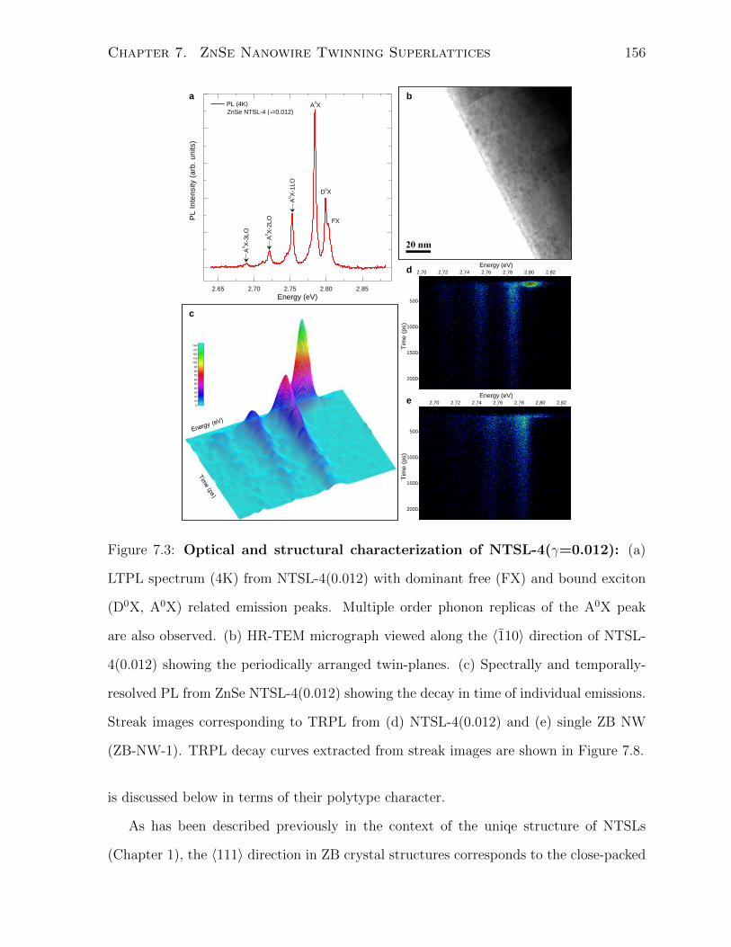
Chapter 7. ZnSe Nanowire Twinning Superlattices 156
2.65 2.70 2.75 2.80 2.85
D0X
FX
A0X
A0X
-1LO
PL (4K)
ZnSe NTSL-4 ( =0.012)
PL
In
ten
sity (
arb
. u
nits)
Energy (eV)
A0X
-2LO
A0X
-3LO
2.70 2.72 2.74 2.76 2.78 2.80 2.82
500
1000
1500
2000
Tim
e (
ps)
Energy (eV)
2.70 2.72 2.74 2.76 2.78 2.80 2.82
500
1000
1500
2000
Tim
e (
ps)
Energy (eV)
a
c
b
d
e
Figure 7.3: Optical and structural characterization of NTSL-4(γ=0.012): (a)
LTPL spectrum (4K) from NTSL-4(0.012) with dominant free (FX) and bound exciton
(D0X, A0X) related emission peaks. Multiple order phonon replicas of the A0X peak
are also observed. (b) HR-TEM micrograph viewed along the 〈110〉 direction of NTSL-
4(0.012) showing the periodically arranged twin-planes. (c) Spectrally and temporally-
resolved PL from ZnSe NTSL-4(0.012) showing the decay in time of individual emissions.
Streak images corresponding to TRPL from (d) NTSL-4(0.012) and (e) single ZB NW
(ZB-NW-1). TRPL decay curves extracted from streak images are shown in Figure 7.8.
is discussed below in terms of their polytype character.
As has been described previously in the context of the uniqe structure of NTSLs
(Chapter 1), the 〈111〉 direction in ZB crystal structures corresponds to the close-packed
Chapter 7. ZnSe Nanowire Twinning Superlattices 157
arrangement of atomic planes in the sequence . . .ABCABC. . ., while for WZ crystal
structure (hexagonal close-packed (hcp)), the sequence is . . .ABAB. . . with each letter
representing a bilayer. The periodically arranged twin-planes in NTSLs perturb this
stacking sequence in one dimension (growth direction) which results in an apparent mirror
symmetry at the twin-plane and the observed side-facets [124, 132]. The result is a
periodic structure with stacking sequence . . .ABCABACBA. . ., with B indicating the
twin-plane where stacking sequence is mirrored. This structure qualifies as a polytype
structure [306] with a repeat unit encompassing one twin-plane and two domains with N
monolayers in each. Thus, a ZnSe NTSL with twin-plane spacing d(= Nd〈111〉) represents
a unique polytype of ZnSe, which can be denoted as 2NH-polytype or equivalently as
(2/γ)H-polytype, and it is clear that the number of such polytypes is infinite. A ZB
structure with no twin boundaries is represented by γ=0, while a WZ structure can be
considered as a stacking with a twin-plane at every atomic plane in 〈111〉-ZB direction
and is denoted as γ=1. NTSL-1(0.100), for example, represents a 20H polytype, and
similarly other higher order O(N) (or O(γ)) polytypes such as 4H (γ=0.5), 6H (γ=1/3),
etc. can be constructed. As another example, in the schematic in Figure 1.2 (e), the
repeat unit corresponds to the two twin-planes labelled C and separated by a distance
2d. In this case N=5 and the NTSL represents a 10H polytype. Such polytypes would
possess unique properties individually, and gradually varying overall with γ between two
extremes represented by ZB and WZ ZnSe. In particular, the Eg is expected to vary
between ZB and WZ band gaps with varying γ and this variation Eg(γ) is demonstrated
experimentally and supported through band-structure calculations below.
7.1.2 Excitation intensity dependence of LTPL
LTPL was also studied as a function of Iexc for individual NTSLs. Bao et al [133] have
previously studied LTPL from randomly twinned InP NWs (RTNWs) with varying Iexc
and observed a blue-shift in PL peak position with increasing Iexc. They assumed the
Chapter 7. ZnSe Nanowire Twinning Superlattices 158
existence of one monolayer of WZ InP arising due to . . .ABA. . . stacking sequence at
the twin-plane and related their observed blue-shift to band filling effect arising due to
staggered band-alignment between ZB and presumed WZ segments. This interpretation
that twinning leads to a type-II band alignment at the twin-plane has been accepted by
many authors [132,206]. However, the perturbation in potential introduced by the twin-
plane (B) in an otherwise extended . . .ABCABCABACBACBA. . . stacking sequence
is too weak to localize electrons or holes required for spatially indirect PL transitions.
The argument of type-II (staggered) band-alignment is however valid for a true WZ-ZB
superlattice structure consisting of extended ZB and WZ domains, and would lead to a
blue-shift in PL when Iexc is increased which has been observed experimentally by Pe-
masiri et al [127] on InP WZ NWs containing ZB segments. Caroff et al [122, 124] have
also dismissed Bao et al’s [133] interpretation and argued that NTSLs be considered as
periodic twinning based polytype structures. Thus, the PL transitions in NTSLs are
direct, and no blue-shift in PL peak position(s) is expected with varying Iexc (excluding
the high excitation regime). LTPL spectra from NTSL-6(0.019) with increasing Iexc and
the corresponding change in peak energies for individual emission peaks are shown in
Figures 7.4 and 7.5, respectively. No blue-shift was observed in any emission peak. Fur-
ther, no blue-shift was observed in PL peak positions in a similar Iexc-dependent LTPL
experiment on a RTNW. Thus, based on Iexc-dependent LTPL experiments, it is clear
that NTSLs behave as polytype structures with no evidence of staggered band-alignment.
This is also supported by ab Initio calculations discussed briefly below. Figure 7.4 shows
excitation intensity (Iexc) dependent PL spectra from NTSL-6(γ=0.019), where Iexc was
varied from 6.25 W/cm2 to 500 W/cm2. All spectra were recorded at a constant temper-
ature (4± 1 K), and were fitted to individual emission peaks using Lorentzians. Change
in peak position for two such emission peaks is shown in Figure 7.5 with varying Iexc.
The PL peaks showed a slight red-shift, not exceeding 4 meV, related to the unavoidable
laser heating under ultra-fast optical excitation conditions and irrelevant to the discussion

Chapter 7. ZnSe Nanowire Twinning Superlattices 159
here.
2 . 7 0 2 . 7 5 2 . 8 0 2 . 8 5 2 . 9 0 2 . 9 5
P 0 = 6 . 2 5 W / c m 2
P 0
2 P 0
4 P 0
PL In
tensity
(arb.
units)
E n e r g y ( e V )
2 0 P 0
4 0 P 0
6 0 P 0
8 0 P 0
8 P 0
Figure 7.4: Variation in LTPL spectra obtained from NTSL-5(0.019) as a function of
excitation intensity Iexc. All spectra were acquired at a constant temperature (4 K),
normalized to unity and are displayed offset for clarity.
7.2 Variation in band gap of NTSLs
The variation in electronic structure and optical properties of NTSLs with varying γ is
discussed below. The electronic band gap of ZB ZnSe is 2.822 eV at 0K [7]. Liang and

Chapter 7. ZnSe Nanowire Twinning Superlattices 160
0 1 0 0 2 0 0 3 0 0 4 0 0 5 0 02 . 8 0 0
2 . 8 0 5
2 . 8 1 0
2 . 8 1 5
2 . 8 2 0
Peak
energ
y (eV
)
E x c i t a t i o n I n t e n s i t y ( W / c m 2 )
Figure 7.5: Change in peak energies as a function of Iexc for two individual emission peaks
observed in the LTPL from NTSL-5(0.019). Each spectrum shown in Figure 7.4 was fit
to individual emission peaks using Lorentzians, and the peak energies thus obtained are
shown with varying Iexc. The solid lines are guide to the eye.

Chapter 7. ZnSe Nanowire Twinning Superlattices 161
Yoffe [238] have reported the energy band gap of WZ ZnSe as Eg,WZ=2.874 eV, and
this value has been widely accepted in the literature. Similar to the case of ZB NWs,
the LTPL spectrum from a single WZ NW was experimentally obtained (Chapter 6),
and the Eg was found to agree well with the value reported by Liang and Yoffe [238].
Figure 7.6 (a) shows the variation in PL spectra for NTSLs with different periodicity
parameters (γ) representing polytypes of different orders (also indicated), ZB and WZ
NWs. The corresponding HR-TEM micrographs are shown in Figure 7.6 (b) taken at
similar magnification factors. Note, that the LTPL spectra and HR-TEM micrographs
in Figure 7.6 for ZB (γ=0) and WZ NWs (γ=1) are those of ZB-NW-1 and WZ-NW-1
presented in Chapters 5 and 6, respectively. It is noted that the NTSLs denoted by ∗ in
Figure 7.6 (a) showed PL peaks corresponding to the emission from the band-edges of
NTSLs. This is due to the influence of hole-traps in ZnSe which are also responsible for
the phenomenon of persistent photoconductivity in ZnSe, combined with the ultra-fast
excitation conditions. This phenomenon has been observed experimentally for heavily n-
doped ZnSe epilayers [307–309], and discussed further using dependence of LTPL spectra
and LTPL peak positions on temperature later in this chapter. Thus, it is observed that
the PL peak positions from NTSLs monotonically shift to higher energies with increasing
periodicity parameter γ, but not exceeding that of the band gap of WZ ZnSe. For NTSLs
exhibiting free exciton emission the band gaps were estimated using an exciton-binding
energy EFX of 21 meV [7]. This is meaningful since the EFX in WZ ZnSe has been shown
to be similar to that of ZB ZnSe (difference=1 meV) [238], and thus a change in EFX
for NTSLs would be <1 meV. This may not be true for NTSLs based on other III-V and
II-VI compound semiconductors. The variation in band gaps of NTSLs with γ is shown
in Figure 7.7. NTSLs with γ values up to 0.33 were studied. The end-points with γ=0
and 1 correspond to the pure ZB and WZ crystal structures of ZnSe, respectively. The
variation in band gap is near linear.
The electronic structures for NTSLs were calculated using ab Initio pseudo-potential

Chapter 7. ZnSe Nanowire Twinning Superlattices 162
method, the details of which can be found in the Appendix E.2. As is well-known,
this method of electronic structure calculations significantly underestimates the band
gaps [310]. For comparison with the experimental values, a constant shift (known as
a scissors-shift) of 1.642 eV was applied uniformly to all structures so as to align the
calculated band gap of ZB ZnSe with the experimental value. The band gaps for all
NTSLs were found to be direct, and folded in k-space as required by the periodicity. See
Figures E.3 and E.4 in the Appendix E.2, for the calculated electronic structures of 2H,
4H and 6H structures. As shown in Figure 7.7, the calculated band-gap as a function
of γ shows a near linear variation with the band-gap gradually increasing from pure
ZB structure to pure WZ structure by about 63 meV. These features are in excellent
agreement with the experiments and provide support for the assignment of the LTPL
peaks discussed above. Based on the above discussion, the energy band gap of NTSLs as
a function of γ can be expressed as
Eg(γ) = Eg,ZB + (Eg,WZ − Eg,ZB)γ (7.1)
7.3 Time-resolved photoluminescence
Time-resolved PL (TRPL) provides useful information regarding the radiative and non-
radiative recombination channels. Bao et al. [133] have further speculated in support
of their hypothesis that the PL lifetimes in RTNWs would be longer than homogeneous
ZB or WZ NWs due to the spatial separation of electrons and holes at the twin-plane
interfaces. It was argued that this spatial separation of electrons and holes would require
more time for them to recombine, and hence result in longer PL lifetimes. This was as-
cribed to the monolayer WZ sections, assumed to exist at the twin boundaries, localizing
the holes, while electrons being localized in the extended ZB domains. This change in PL
lifetimes was experimentally observed in heterostructure NWs with extended ZB and WZ
domains in InP NWs [127]. However, as explained earlier, the perturbation in potential

Chapter 7. ZnSe Nanowire Twinning Superlattices 163
2.75 2.80 2.85 2.90
2 H
104 H
168 H
34 H
26 H
PL
In
ten
sity (
arb
. u
nits)
Energy (eV)
=0
=0.077*
=0.100*
=1
=0.059*
=0.019*
=0.012
20 H
a b
Fig
ure
7.6:
Vari
ati
on
inP
Lsp
ect
raas
afu
nct
ion
of
peri
odic
ity
para
mete
rγ:
(a)
LT
PL
(4K
)sp
ectr
aob
tain
edfr
om
five
diff
eren
tN
TSL
sw
ith
vary
ing
per
iodic
ity
par
amet
ersγ
.P
erio
dic
ity
par
amet
erγ
and
the
order
ofth
ep
olyty
pe
(2/γ
)H(o
r
2NH
)ar
ein
dic
ated
inth
efigu
re.
Als
osh
own
are
the
exp
erim
enta
lly
obta
ined
PL
spec
tra
from
singl
eZ
B(γ
=0)
,an
dsi
ngl
e
WZ
(2H
)(γ
=1)
NW
s.T
her
eis
am
onot
onic
blu
e-sh
ift
inLT
PL
spec
tra
wit
hin
crea
singγ
indic
atin
gth
ein
crea
sein
ener
gyban
d
gap
for
pol
yty
pes
ofZ
nSe
wit
hm
axim
um
ban
dga
pfo
rW
ZZ
nSe.
(b)
HR
-TE
Mm
icro
grap
hs
corr
esp
ondin
gto
the
NT
SL
s(γ
),
ZB
and
WZ
NW
sw
hos
eLT
PL
spec
tra
are
dis
pla
yed
in(a
).T
he
HR
-TE
Mm
icro
grap
hs
wer
eta
ken
atsi
milar
mag
nifi
cati
on
fact
ors
alon
g〈1
10〉
zone-
axis
.
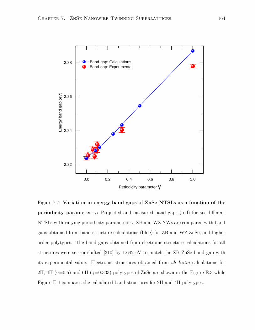
Chapter 7. ZnSe Nanowire Twinning Superlattices 164
0 . 0 0 . 2 0 . 4 0 . 6 0 . 8 1 . 0
2 . 8 2
2 . 8 4
2 . 8 6
2 . 8 8 B a n d - g a p : E x p e r i m e n t a l
Energ
y ban
d gap
(eV)
P e r i o d i c i t y p a r a m e t e r γ
B a n d - g a p : C a l c u l a t i o n s
Figure 7.7: Variation in energy band gaps of ZnSe NTSLs as a function of the
periodicity parameter γ: Projected and measured band gaps (red) for six different
NTSLs with varying periodicity parameters γ, ZB and WZ NWs are compared with band
gaps obtained from band-structure calculations (blue) for ZB and WZ ZnSe, and higher
order polytypes. The band gaps obtained from electronic structure calculations for all
structures were scissor-shifted [310] by 1.642 eV to match the ZB ZnSe band gap with
its experimental value. Electronic structures obtained from ab Initio calculations for
2H, 4H (γ=0.5) and 6H (γ=0.333) polytypes of ZnSe are shown in the Figure E.3 while
Figure E.4 compares the calculated band-structures for 2H and 4H polytypes.

Chapter 7. ZnSe Nanowire Twinning Superlattices 165
0 5 0 0 1 0 0 0 1 5 0 0 2 0 0 0
τ1 = 1 4 7 p s , τ2 = 6 6 1 p s
T R P L D e c a y N T S L - 4 ( 0 . 0 1 2 )
PL In
tensity
(arb.
units)
T i m e ( p s )
τ1 = 2 4 p s , τ2 = 6 0 6 p s
T R P L D e c a y Z B - Z n S e N W
Figure 7.8: Low-temperature photoluminescence (4 K) decay from NTSL-4(0.012) (red)
and single ZB NW (ZB-NW-1 from Chapter 5) (blue) extracted from the streak images
shown in Figures 7.3 (d) and (e), respectively, with an energy window of 20 meV centred
around the acceptor-bound exciton peak (A0X) (the strongest peak). Both decay curves
are characterized by a bi-exponential decay with comparable lifetimes as shown.
at twin-planes in NTSLs is insufficient to localize holes, and thus such an increase in PL
lifetimes is not expected. In fact, the PL lifetimes from NTSLs and RTNWs would be
comparable to those from the homogeneous NWs, dictated primarily by the oscillator
strengths of relevant transitions. As discussed earlier, the calculated electronic structure
indeed shows that the transition dipole moments and hence the oscillator strengths for
inter-band transitions are nearly independent of the periodicity. Figure 7.3 (c) shows
Chapter 7. ZnSe Nanowire Twinning Superlattices 166
spectrally and temporally resolved PL decay from NTSL-4(0.012) with distinguishable
decay channels for different exciton emissions. Figures 7.3 (d) and (e) are the streak
images representing PL decay obtained from NTSL-4(0.012) and single ZB NW (ZB-
NW-1), respectively. It is readily observed that the PL decay is similar in both cases and
TRPL decay curves extracted from the two streak images yield similar PL lifetimes as
shown in the Figure 7.8.
7.4 Dependence of PL on temperature
PL from NTSL-7(γ=0.014) was measured as a function of temperature, and the variation
in PL with temperature is shown in the Figure 7.9 for temperatures up to 150 K. Each
LTPL spectrum was fit to the individual emission peaks, and the fit parameters obtained
are discussed next. Figure 7.10 shows the change in peak energy for the highest energy
peak (2.82 eV) at different temperatures for NTSL-7(0.014) (red). This peak is related
to the band gap of NTSL-7 corresponding to the recombination of free carriers. The solid
and dashed lines are fits to Equations 5.3 (Varshni’s equation) and 5.4 (Bose-Einstein
type expression), respectively. The parameters obtained from these fits are listed in
Table 7.2, where α represents the temperature gradient (dEg/dT ) of the band gap of
NTSL-7. Experimentally obtained peak positions of the free exciton peak at different
temperatures for ZB NW are also shown in Figure 7.10, with solid and dashed lines
representing the fits to Equations 5.3 and 5.4, respectively. The fit parameters are also
listed in Table 7.2. (These were determined earlier in Chapter 5 for ZB-NW-4). It
was explained in Chapter 6 that the temperature gradient of WZ NWs could not be
determined based on the dependence of PL on temperature, since the FX peak was not
observed in WZ NWs. However, Liang and Yoffe [305] have reported the energy positions
of free exciton absorption at four temperatures based on their absorption experiments
on WZ ZnSe single crystals. These values are shown in Figure 7.10 along with the fits to
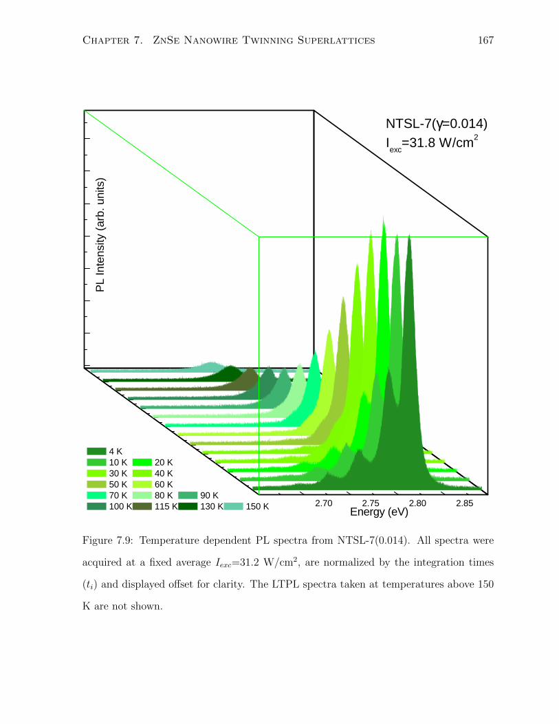
Chapter 7. ZnSe Nanowire Twinning Superlattices 167
2 . 7 0 2 . 7 5 2 . 8 0 2 . 8 5
N T S L - 7 ( γ= 0 . 0 1 4 )I e x c = 3 1 . 8 W / c m 2
4 K 1 0 K 2 0 K 3 0 K 4 0 K 5 0 K 6 0 K 7 0 K 8 0 K 9 0 K 1 0 0 K 1 1 5 K 1 3 0 K 1 5 0 K
PL In
tensity
(arb.
units)
E n e r g y ( e V )Figure 7.9: Temperature dependent PL spectra from NTSL-7(0.014). All spectra were
acquired at a fixed average Iexc=31.2 W/cm2, are normalized by the integration times
(ti) and displayed offset for clarity. The LTPL spectra taken at temperatures above 150
K are not shown.

Chapter 7. ZnSe Nanowire Twinning Superlattices 168
Table 7.2: Values of the fit parameters of Equations 5.3 (Varshni’s equation) and 5.4
(Bose-Einstein type expression) which describe the temperature dependence of the Eg.
Process Eg(0) α β Source
(eV) (10−4 eV/K) (K)
WZ ZnSe FX 2.853 ± 0 5.0 ± 0.8 139.7 ± 68.7 Ref. [238]
NTSL-7(0.014) Eg 2.820 ± 0 6.5 ± 0.4 222.6 ± 27.8 Expt.
ZB-NW-3 FX 2.799 ± 0 8.9 ± 0.7 361.5 ± 44.8 Expt. (Chapter 5)
Process Eg(0) αB θB Source
(eV) (meV) (K)
WZ ZnSe FX 2.852 ± 0 30.9 ± 2.0 143.8 ± 7.3 Ref. [305]
NTSL-7(0.014) Eg 2.818 ± 0 45.4 ± 1.5 183.4 ± 4.4 Expt.
ZB-NW-3 FX 2.797 ± 0 56.5 ± 4.7 209.3 ± 11.6 Expt. (Chapter 5)
Equations 5.3 (solid line) 5.4 (dashed line). The fit parameters from these are also listed
in Table 7.2. It is important to note that the dEg/dT for NTSL-7 lies between those of ZB
and WZ ZnSe. This further supports the claim that ZnSe NTSLs are polytype structures
of ZnSe in which case their physical properties would be expected to lie between those
of the ZB and WZ ZnSe.
The change in IPL with temperature for NTSL-7(0.014) is shown in Figures 7.11 (a,b)
for the (a) free-carrier recombination and (b) VSe-related donor bound exciton emission,
respectively. The solid lines are fits to the one process thermal quenching model (Equa-
tion 5.6). The activation energy for thermal quenching for free-carrier recombination
was found to be 20 meV. For the (D0X) emission, the activation energy was found to
be 7 meV which is identical to the binding energy of (D0X) excitons (discussed in detail
in Chapter 4). The change in linewidth (HWHM) with temperature for the band gap
recombination from NTSL-7(0.014) is shown in Figure 7.12, where the solid line is a fit
to the expression in Equation 5.5. Note that in this case the second and third terms

Chapter 7. ZnSe Nanowire Twinning Superlattices 169
0 5 0 1 0 0 1 5 0 2 0 0 2 5 0 3 0 02 . 7 0
2 . 7 2
2 . 7 4
2 . 7 6
2 . 7 8
2 . 8 0
2 . 8 2
2 . 8 4
2 . 8 6
Energ
y (eV
)
T e m p e r a t u r e ( K )
W Z - Z n S e B u l k ( F X ) - R e f . N T S L - 7 γ ( 0 . 0 1 4 ) E g - E x p t . Z B - N W - 3 ( F X ) - E x p t . F i t F i t
Figure 7.10: Variation in PL peak energy of the emission corresponding to the band gap
recombination (red, for NTSL-7(0.014)) with temperature. Change in PL peak energy
for the FX emission for ZB-NW-3 (green, experimental) and energies corresponding to
the FX absorption for WZ ZnSe [238] (blue) are also shown. The solid and dashed lines
in each case are fits to the Equations 5.3 and 5.4, respectively.
on the right side in Equation 5.5 represent the interaction of electron with acoustic and
optical phonons, respectively. The parameters obtained from the fit are listed in Ta-
ble 7.3. For comparison these parameters obtained for the FX emission from ZB-NW-4
(in Chapter 5) are also listed. The term representing inhomogeneous broadening (Γinh) is
larger for NTSL-7 compared to that for ZB-NW-4, and this is due to the phenomenon of
screening of excitons. The value of ΓLO is comparable in both cases, while γth is almost
half for NTSL-7 compared to that for ZB-NW-4.
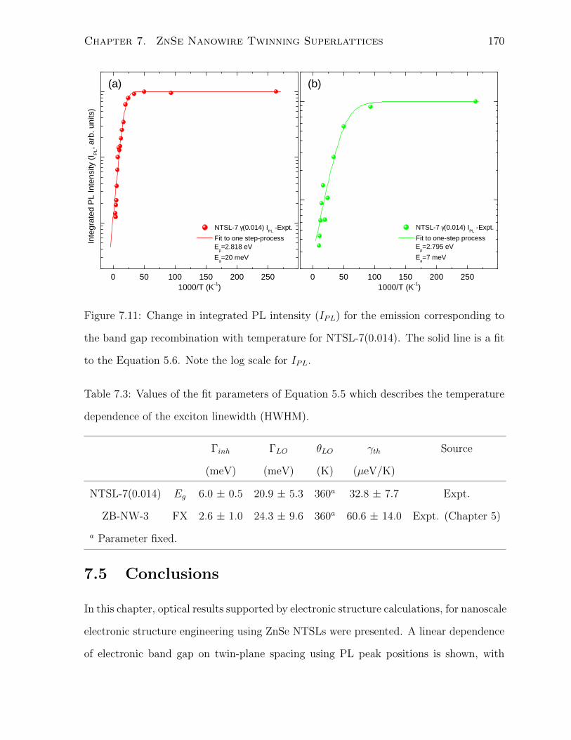
Chapter 7. ZnSe Nanowire Twinning Superlattices 170
0 5 0 1 0 0 1 5 0 2 0 0 2 5 0
( b )
1 0 0 0 / T ( K - 1 )
N T S L - 7 γ( 0 . 0 1 4 ) I P L - E x p t . F i t t o o n e s t e p - p r o c e s s
E p = 2 . 8 1 8 e V E a = 2 0 m e V
Integ
rated
PL In
tensity
(I PL, a
rb. un
its)
1 0 0 0 / T ( K - 1 )
( a )
0 5 0 1 0 0 1 5 0 2 0 0 2 5 0
N T S L - 7 γ( 0 . 0 1 4 ) I P L - E x p t . F i t t o o n e - s t e p p r o c e s s
E p = 2 . 7 9 5 e V E a = 7 m e V
Figure 7.11: Change in integrated PL intensity (IPL) for the emission corresponding to
the band gap recombination with temperature for NTSL-7(0.014). The solid line is a fit
to the Equation 5.6. Note the log scale for IPL.
Table 7.3: Values of the fit parameters of Equation 5.5 which describes the temperature
dependence of the exciton linewidth (HWHM).
Γinh ΓLO θLO γth Source
(meV) (meV) (K) (µeV/K)
NTSL-7(0.014) Eg 6.0 ± 0.5 20.9 ± 5.3 360a 32.8 ± 7.7 Expt.
ZB-NW-3 FX 2.6 ± 1.0 24.3 ± 9.6 360a 60.6 ± 14.0 Expt. (Chapter 5)
a Parameter fixed.
7.5 Conclusions
In this chapter, optical results supported by electronic structure calculations, for nanoscale
electronic structure engineering using ZnSe NTSLs were presented. A linear dependence
of electronic band gap on twin-plane spacing using PL peak positions is shown, with

Chapter 7. ZnSe Nanowire Twinning Superlattices 171
0 5 0 1 0 0 1 5 0 2 0 0 2 5 0 3 0 05
1 0
1 5
2 0
2 5
3 0
HWHM
(meV
)
T e m p e r a t u r e ( K )
N T S L - 7 γ ( 0 . 0 1 4 ) H W H M - E x p t . F i t
Figure 7.12: Change in HWHM for the band gap recombination with temperature for
NTSL-7(0.014). The solid line is a fit to the Equation 5.5.
band gap that varies between their values in ZB and WZ crystal structures. NTSLs are
thus unique polytypes of the parent material and possess electronic and optical prop-
erties governed only by the twin-plane spacing. Since NWs have the unique ability to
crystallize as NTSLs a similar variation in band gaps of NTSLs based on other III-V
and II-VI compound semiconductors is expected thus adding a new dimension to NW
functionality. The optical performance of NTSLs was shown to be comparable to those
of homogeneous NWs, based on a comparison of their Γp and IPL. The experimental
evidence of band-structure engineering using periodically arranged twin-planes combined
with their cost-effective synthesis presented here should open the possibility of opto-
electronic device fabrication using nanostructured materials with on-demand engineered
properties.

Chapter 7. ZnSe Nanowire Twinning Superlattices 172
Dependence of PL on temperature was also studied for a single NTSL, and parameters
α, β, αB, and θB related to the dependence of Eg on temperature were determined. These
were found to be intermediate between those for ZB and WZ crystal structures. The
other parameters that were extracted include those related to inhomogeneous broadening
(Γinh=6.0±0.5), strength of the exciton-acoustic phonon (γth=32.8±7.7) and exciton-LO
phonon (ΓLO=20.9±5.3) interactions. The activation energy for thermal quenching of
band gap luminescence was found to be 20 meV, while that for donor-bound exciton
emission as 7 meV.
Chapter 8
Conclusions and Outlook
Experimental demonstration of the nanoscale band-structure engineering was presented
using extensive optical and structural characterization on individual ZnSe based NTSLs,
supported by ab Initio band-structure calculations. It was shown that the Eg and the
electronic band structure of ZnSe NTSLs systematically vary with their twin-plane spac-
ing, and that NTSLs represent a new class of nanoscale polytype structures. Each of
these essentially infinite number of polytypes, similar to bulk polytypes [311], possesses
characteristic physical properties governed by their twin-plane spacing (d). A linear vari-
ation in Eg was shown through a monotonic shift in PL peak position from ZnSe NTSLs
as a function of their twin-plane spacing, which was quantified by using a periodicity pa-
rameter γ. It was shown that the Eg of a ZnSe NTSL lies between the Eg of ZnSe in ZB
and WZ crystal structures, and depends only on γ. It was also established that a widely
used model that TSLs can be interpreted as ZB-WZ superlattices is not appropriate for
describing the electronic structure of NTSLs. The linewidths and integrated PL intensi-
ties in PL from NTSLs were shown to be comparable to those from homogeneous NWs,
thus demonstrating that the periodic twin-planes in NTSLs have no adverse effect on the
optical response of NTSLs. The periodic twin-planes in NTSLs lead to new materials
with characteristic optical properties in contrast to the view of twin-planes as defects
173

Chapter 8. Conclusions and Outlook 174
that should be avoided. NTSLs studied in this work were synthesized via a cost-effective
method which is a significant advantage in terms of their potential applications.
Temperature dependence of PL from a single NTSL was used to determine the pa-
rameters in Varshni’s equation and Bose-Einstein type expression, which describe the
temperature dependence of Eg. These were found to lie between those of ZB and WZ
crystal structures. The dependence of linewidth of band gap related luminescence was
used to determine the parameters related to broadening of luminescence lines. The
constants for coupling between exciton-acoustic phonon and exciton-LO phonon were
deduced. The band gap luminescence was quenched with increasing temperatures with
an activation energy of 20 meV. The activation energy for thermal quenching of neutral
donor-bound exciton emission at 2.795 eV was 7 meV, in agreement with the binding
energy of the donor-bound excitons. The identification of recombination lines in NTSLs
was based on an unambiguous pre-determination of the recombination centres in NWs
with varying stoichiometry, and for ZB and WZ NWs in direct relation to their crystal
structure, as summarized below.
LTPL from NWs was studied as a function of modulation of their stoichiometry. This
was achieved by their growth in the conditions of excess of Zn and excess Se. LTPL
from excess Zn NWs was also studied with varying Iexc. For NWs with excess Zn, strong
emission related to excitons bound to neutral donors was observed at 2.794 eV. The
binding energy of the exciton to the neutral donor, identified as VSe, was determined to
be 7 meV, and the ionization energy of the donor as 35 meV. Two peaks at 2.714 eV
and 2.686 eV due to DAP recombinations were also observed. Based on the dependence
of LTPL on Iexc, the binding energies for both the donors associated with these DAP
recombinations were calculated to be 27±1 meV, whereas those of the acceptors as 102.5
meV and 139 meV, respectively. These donors and acceptors were ascribed to the defect
complexes formed by single native point defects such as VSe, VZn, Zni and Sei with other
native defects. Y-line emission, which is related to the presence of structural defects such

Chapter 8. Conclusions and Outlook 175
as stacking faults and dislocations in ZnSe was also observed. The LTPL from NWs
with excess Se was compared with that from NWs with excess Zn. The emission line
related to the excitons bound to neutral donors at VSe, observed in the case of NWs with
excess Zn, was absent in the case of NWs with excess Se. No other exciton-related line
was observed in the latter case, and the LTPL spectrum was dominated by DL emission
bands at 2.27 eV and 1.96 eV. These DL emissions were related to the presence of VZn
in the NWs with excess Se. These observations confirm that the optical transitions in
ZnSe NWs are primarily dictated by the native point defects.
The optical response from single ZB ZnSe NWs was studied using LTPL. The crystal
structure of these NWs was confirmed to be ZB, with a single crystalline microstructure
using TEM, HR-TEM and SAD. The optical emission was found to be dominated by the
native point defects, while no emission peaks related to the unintentional impurities were
detected. This confirms the observation noted above that the optical properties of ZnSe
NWs are governed only by the native point defects. Two strong PL lines were observed
at 2.785 eV and 2.780 eV. Both of these were assigned to the excitons bound to deep
neutral acceptors related to VZn and (VZn-complex), respectively. These were labelled
as Id1 and Id′
1 lines, respectively. The binding energies of the excitons responsible for the
Id1 and Id′
1 lines are 15 meV and 20 meV, respectively, and the ionization energy of the
associated deep acceptors are 150 meV and 200 meV, respectively. The Id1 and Id′
1 lines
were accompanied by their LO-phonon replicas, which are characteristic of the excitons
bound to deep neutral acceptors. The phonon-replicas of up to 3 orders were observed for
both lines, and the average number of emitted phonons was found to be 0.53 < Nph < 0.7
for the Id1 line, and 0.25 < Nph < 0.42 for the Id′
1 line. Another recombination peak at
2.800 eV was also observed, and related to the free-exciton (FX) emission in ZnSe. These
findings on the Id1 and Id′
1 lines, their phonon-replicas as well as the number of emitted
LO phonons have not been reported thus far in ZnSe NWs.
Excitonic emission linewidths of ∼1.5 meV for the Id1 line were observed in single ZB
Chapter 8. Conclusions and Outlook 176
NWs, which are the narrowest excitonic linewidths reported so far on ZnSe NWs. The
narrowest linewidth previously reported is 10 meV for ZnSe NWs grown by MOCVD
method. The observation of excitonic lines with linewidths close to 1 meV from NWs
grown by CVD growth method in the present case shows that the crystalline quality and
the optical performance of NWs synthesized by the CVD method are comparable to those
from other expensive and time-consuming methods. These narrow linewidths are also
comparable to the narrowest reported linewidths in PL from NWs of other semiconductor
materials. The optical response from a single NW was compared with that from a bundle
of NWs. It was found that the energy position of recombination lines are identical in
both cases, and the Y-line emission related to structural defects was not observed in
either case. This confirms that the Y-line emission actually does not originate from
homogeneous NWs, but rather from the growth of crystallites of ZnSe on the sample
substrate beneath the layer of NWs. The linewidths of the excitonic Id1 emission from
the bundle of NWs were slightly larger than those from single NWs, due to the ensemble
broadening. The linewidths of the Id1 line in different NWs were also slightly different,
and the ensemble broadening effect can also be understood by considering that in the
case of a bundle of NWs, the broadening is limited by the NW which exhibits the largest
linewidths.
PL from single ZB NWs was measured at varying temperatures. The assignment of
the emission peak at 2.800 eV to FX was confirmed by the temperature dependence of
the peak energy of this emission. This was also used to determine the high-temperature
limit of dEg/dT , which was found to be in excellent agreement with the values reported
in the literature for bulk ZnSe. The parameters of the Bose-Einstein type expression
were determined for the FX emission, and found to be in good agreement with those
previously reported for bulk ZnSe. These parameters were also deduced for the Id1 and
Id′
1 lines using dependence of their peak energy on temperature. The change in HWHM
with temperature for the FX emission, Id1 and Id′
1 lines revealed a small contribution of
Chapter 8. Conclusions and Outlook 177
the inhomogeneous broadening to the linewidths. This is consistent with the observation
of narrow linewidths for the Id1 and Id′
1 lines. A strong exciton-acoustic phonon and
exciton-LO phonon coupling was found for these lines in accord with the observation of
LO-phonon replicas in the PL spectra, and large average number of emitted phonons for
these lines. The integrated PL intensity of the FX emission was quenched with increasing
temperatures by two mechanisms. The first mechanism with an activation energy of 20
meV is related to the dissociation of free excitons with a binding energy of 21 meV. The
other mechanism with an activation energy of 136 meV could be a result of non-radiatve
recombination related to surface recombination. The Id1 and Id′
1 line were quenched
with increasing temperatures by mechanisms with activation energies smaller than their
binding energies. These are proposed to be due to non-radiative recombination induced
by scattering of excitons responsible for these lines with the simultaneously emitted LO-
phonons.
The optical response of single WZ NWs was studied using LTPL, and similar to
the case of ZB NWs, their crystal structure and single crystalline microstructure was
confirmed using structural characterization techniques. The centres responsible for the
recombination lines were identified based on the previous work by Liang and Yoffe [305]
and by reference to the identification of PL lines in ZB NWs. Similar to the ZB NWs, the
optical properties were dictated by the native point defects in WZ NWs. Two lines related
to the excitons bound to neutral acceptors were observed, but only one of them was due
to the deep acceptors. A recombination line at 2.841 eV, labelled as I1, was assigned to
VZn as neutral acceptors. The binding energy of this exciton is 11 meV, and the ionization
energy of the acceptor 110 meV. Another recombination line at 2.833 eV, labelled as Id1 ,
was ascribed to the excitons bound to deep neutral acceptors related to (VZn-complex),
by reference to their observation in ZB NWs. The binding energy of the exciton and the
ionization of the acceptor are 19 meV and 190 meV, respectively. DAP related transitions
were also observed in the LTPL spectra from WZ NWs, along with their phonon-replicas

Chapter 8. Conclusions and Outlook 178
of up to 3 orders. The average number of phonons was found to be 0.69, identical to that
reported by Liang and Yoffe [305]. Other transitions observed in the LTPL spectra were
assigned to the simultaneous emission of acoustic and optical phonons, and a transition
scheme was proposed. This recombination scheme is an extension of the one proposed
by Liang and Yoffe [305] for different peaks. This is the first time since the report on PL
from WZ ZnSe by Liang and Yoffe [305] that a recombination scheme has been proposed.
Linewidths of ∼2.8 meV were obtained for the I1 line, and these are the narrowest
linewidths reported for WZ ZnSe NWs. PL from single WZ NWs was also measured
as a function of temperature. The parameters of the Bose-Einstein type expression for
the dependence of Eg on temperature were determined for the I1 and Id1 lines. The
parameters related to inhomogeneous broadening of the exciton lines, strengths of the
exciton-acoustic phonon and exciton-LO phonon coupling were deduced for the I1 line
from the dependence of HWHM on temperature. The integrated PL intensity of the I1
line was quenched by a mechanism with an activation energy of 9 meV, similar to the
binding energy of the excitons responsible for the I1 line. The centres responsible for
recombination lines identified in this thesis, binding energies of the excitons, and ioniza-
tion energies of the donors and acceptors are summarized in Table 8.1. The parameters
determined using the dependence of PL on temperature for single ZB and WZ NWs and
a single NTSL are summarized in Table 8.2. These parameters for the ZB and WZ NWs
were compared in Chapter 6 for lines due to similar recombination mechanisms.
It needs to be emphasized that the above work would not have been possible without
the implementation of a new experimental methodology, which is also an important
contribution of this thesis. The new approach was based on the cost-effective design
of a sample-holder to bridge the techniques of optical characterization (PL and TRPL)
and structural characterization (TEM). The sample-holder allows one to overcome the
critical challenge of incompatibility in different sample preparation methods required for
these characterization techniques. The use of these techniques independently is quite

Chapter 8. Conclusions and Outlook 179
common for semiconductor characterization, but their combined use provides a powerful
means to remove unambiguities in the interpretation of optical emission spectra. The
sample-holder was used to hold the TEM grids during the optical characterization, which
were removed from it for the TEM characterization. The sample holder allows the use
of the same TEM grid multiple times, with careful handling of the fragile grids. This is
useful, e.g., (i) if more NTSLs or NWs are to be studied on the same grid, and (ii) for
further PL and TRPL experiments.
In a broader perspective, it was shown that:
1. NWs of semiconductor materials can crystallize in unique variations, NTSLs, which
are not known to occur in the bulk form for most materials, including ZnSe. NTSLs are
based on a periodic arrangement of twin-planes in NWs along their growth direction,
which is 〈111〉 in ZB structures.
2. NTSLs are new nanoscale polytypes of their parent materials, essentially infinite in
number, with physical properties, such as Eg, intermediate to those of the parent material
in the ZB and WZ crystal structures. Since the strategies employed thus far, e.g. by a
change in the diameter, strain and composition, proved ineffective in yielding NWs with
tunable optoelectronic properties and desired performance, NTSLs provide an attractive
alternative to achieving this tunability.
3. Further to the above, the optical performance of NTSLs was shown to be at par with
those of homogeneous NWs. This is important because, but for this parity, the tunable
properties offered by NTSLs would have little significance in practical applications.
4. The NWs synthesized using a fast and low-cost CVD method, following a VLS growth
mechanism, show excellent crystallinity and optical performance, comparable to NWs
obtained using expensive and time-consuming methods such as MBE and MOCVD. This
is an important result which should open the possibility of a large-scale synthesis of NWs
for device applications.

Chapter 8. Conclusions and Outlook 180
Table 8.1: Summary of the recombination lines identified in ZB and WZ ZnSe NWs.
The exciton binding energies (EBX) for donor and acceptor bound excitons, ionization
energies of the donors (ED) and acceptors (EA) are also listed.
Ep (eV) Identification Donor/acceptor EBX ED,EA
(meV) (meV)
ZB ZnSe NWs
2.800 FX free excitons
2.794 D0X VSe(a) 7 35
2.785 (Id1 ) A0X VZn(b) 15 EA=150
2.780 (Id′
1 ) A0X (VZn-complex)(b) 20 EA=200
2.714 DAP defect-complex ED=27±1
EA=102.5
2.686 DAP defect-complex ED=27±1
EA=139
2.603 Y-line extended defects
WZ ZnSe NWs
2.841 (I1) A0X VZn(c) 11 EA=110
2.833 (Id1 ) A0X (VZn-complex)(b) 19 EA=190
2.741 DAP
(a): neutral donors, (b): deep neutral acceptors, (c): neutral acceptors
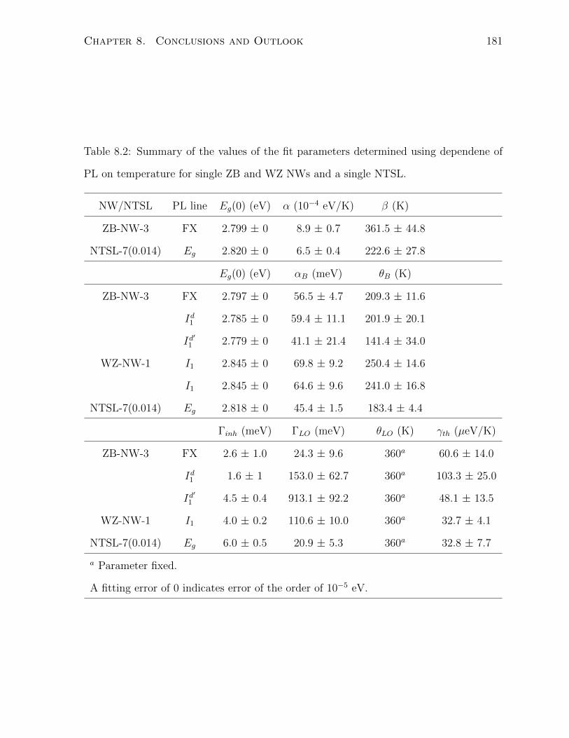
Chapter 8. Conclusions and Outlook 181
Table 8.2: Summary of the values of the fit parameters determined using dependene of
PL on temperature for single ZB and WZ NWs and a single NTSL.
NW/NTSL PL line Eg(0) (eV) α (10−4 eV/K) β (K)
ZB-NW-3 FX 2.799 ± 0 8.9 ± 0.7 361.5 ± 44.8
NTSL-7(0.014) Eg 2.820 ± 0 6.5 ± 0.4 222.6 ± 27.8
Eg(0) (eV) αB (meV) θB (K)
ZB-NW-3 FX 2.797 ± 0 56.5 ± 4.7 209.3 ± 11.6
Id1 2.785 ± 0 59.4 ± 11.1 201.9 ± 20.1
Id′
1 2.779 ± 0 41.1 ± 21.4 141.4 ± 34.0
WZ-NW-1 I1 2.845 ± 0 69.8 ± 9.2 250.4 ± 14.6
I1 2.845 ± 0 64.6 ± 9.6 241.0 ± 16.8
NTSL-7(0.014) Eg 2.818 ± 0 45.4 ± 1.5 183.4 ± 4.4
Γinh (meV) ΓLO (meV) θLO (K) γth (µeV/K)
ZB-NW-3 FX 2.6 ± 1.0 24.3 ± 9.6 360a 60.6 ± 14.0
Id1 1.6 ± 1 153.0 ± 62.7 360a 103.3 ± 25.0
Id′
1 4.5 ± 0.4 913.1 ± 92.2 360a 48.1 ± 13.5
WZ-NW-1 I1 4.0 ± 0.2 110.6 ± 10.0 360a 32.7 ± 4.1
NTSL-7(0.014) Eg 6.0 ± 0.5 20.9 ± 5.3 360a 32.8 ± 7.7
a Parameter fixed.
A fitting error of 0 indicates error of the order of 10−5 eV.
Chapter 8. Conclusions and Outlook 182
5. The ZnSe NWs occur in both ZB and a wider band gap WZ crystal structure, and
exhibit excellent luminescence properties, no inferior to those of NWs based on any other
compound semiconductor, and the best in the blue-region of the spectrum. Further, the
range of optical emission can be tuned as desired using ZnSe NTSLs, which can be easily
obtained by a low-cost synthesis method. ZnSe NWs and NTSLs are therefore ideal
candidates for blue light-emitting optical and optoelectronic devices.
8.1 Outlook
1. The NTSLs studied in this thesis were obtained using their spontaneous growth, i.e.,
with limited control over their occurrence and no control over their periodicities. A precise
control over the periodicty of twin-planes in NTSLs has been demonstrated [124, 132],
but by methods such as MOCVD. Achievement of this control over d in NTSLs with a
CVD growth method would represent a significant advance, and further experiments in
this direction are of practical importance.
2. The strength of electron-LO phonon coupling for NTSL was discussed in this the-
sis. The phonon modes in NTSLs may be further studied using optical techniques such
as Raman spectroscopy. The information presented in this thesis, combined with that
obtained from further experiments including Raman, can be quantitatively related to
phonon back-scattering in NTSLs. This should prove very useful in the design of ther-
moelectric applications based on NTSLs.
3. Further to the above, the experimental methodology employed in this thesis can be
extended to include other techniques of optical characterization such as Raman spec-
troscopy with minor modifications. Note that use of a pulsed laser is not suggested for
Raman spectroscopy because ultra-short pulses result in a broadening of the exciting
laser beam. Other techniques, such as absorption spectroscopy and two-photon absorp-
tion spectroscopy, can be implemented in the experimental arrangement described in this
Chapter 8. Conclusions and Outlook 183
thesis with some modifications.
4. It remains an interesting challenge to find new practical strategies, i.e., beyond the
existing ones mentioned above to widen the range of Eg which NTSLs can assume. Based
on the present work, this range is limited to the difference in Eg between the ZB and WZ
crystal structure of the concerned material. A wider range of Eg’s available for tuning is
an obvious practical advantage.
5. Needless to say, realization of practical devices based on NTSLs, even if on a lab-
oratory scale, is one of the most important advances to look forward to. These may
include applications such as photodetectors and single NW lasers, which have already
been demonstrated for NWs based on ZnSe and other II-VI compound semiconductors.

Appendix A
Bound-exciton lines in ZnSe films
The determined binding energies of the different donor-bound exciton complexes, EBX(D0X),
and the ionization energies of the donors, ED, in ZnSe films are summarized in Table A.1.
These quantities for the acceptor-bound exciton complexes, EBX(A0X) and EA are sum-
marized in Table A.2. These tables are as summarized by Gutowski et al. [7].
184

Appendix A. Bound-exciton lines in ZnSe films 185
Table A.1: Donors and donor-bound excitons in ZnSe films. Line positions at 4.2 K.EBX(D0X) exciton-donor binding energy, ED donor ionization energy, dfilm film thick-ness. Reprinted with permission from Ref. [7] © 1990 John Wiley & Sons.
line EBX(D0X) donor ED dfilm method substrate ref.a
(eV) (meV) (meV) (µm)- Al 26.3 1 to 2 MOCVD ZnSe [130]- Al 30 3 to 4 MOCVD GaAs [136]2.7974 I
′2 Ga 27 to 27.9 1 to 2 MOCVD ZnSe [130]
2.7969 I20 3.8 Ga 0.2 MBE GaAs [118]2.7971 IGa20 4.3(TG = 365◦ C) Ga 1.5 MBE GaAs [109]2.7944 IGa−20 TG = 400◦C Ga 1.5 MBE GaAs [109]2.7966 IGa+20 TG = 400◦C Ga 1.5 MBE GaAs [109]2.7967 IGa20 5.0 Ga 20 MOCVD GaAs [119]2.7950 Ix 5.0 Ga(∗) 1 to 1.5 MBE GaAs [40]2.7969 IGa20 3.9 Ga 0.5 MBE GaAs [122]2.7953 I2 4.7 Ga? 2 to 4 MBE GaAs [44]2.7966 I
′2 3.4 strain-split
Ga 20 3 MBE GaAs [58]2.7949 I2 8.4 Ga 4.9 MBE GaAs [21]- In 28.1 to 28.4 1 to 2 MOCVD ZnSe [130]2.7950 Ix 5.0 In(∗) 1 to 1.5 MBE GaAs [40]- F 29.3 1 to 2 MOCVD [130]- Cl 26.1 to 26.9 1 to 2 MOCVD [130]- Cl 25 2 MBE GaAs [135]2.7954 Ix 4.8 Cl 8 to 20 MBE GaAs [57]2.7965 I20 3.0 Cl? ≥ 2 MBE GaAs [127]2.7945 Ix 5.0 doublet- I 26 3.5 MOCVD GaAs [138]2.7954 Ix 5.5 VSe 3.1 MBE GaAs [121]2.7954 Ix 5.5 VSe? 3 MBE GaAs [94]2.796 Ix 3.5 ? 32 3 MBE GaAs [58]2.7968 I12 3.2 ? 1.4 to 6 MBE GaAs [28]2.7948 I22 5.2 strain-split2.796 I2 ≈ 3 ? 1 MOCVD GaAs [92]2.794 Ix ≈ 5 doublet2.797 I20 3.2 ? 8 to 20 MBE GaAs [57]2.800 Ix 5.4 ? 0.20 MBE GaAs [17](∗) Author claims Ix to be related to Ga or In.a References are those in Reference [7].
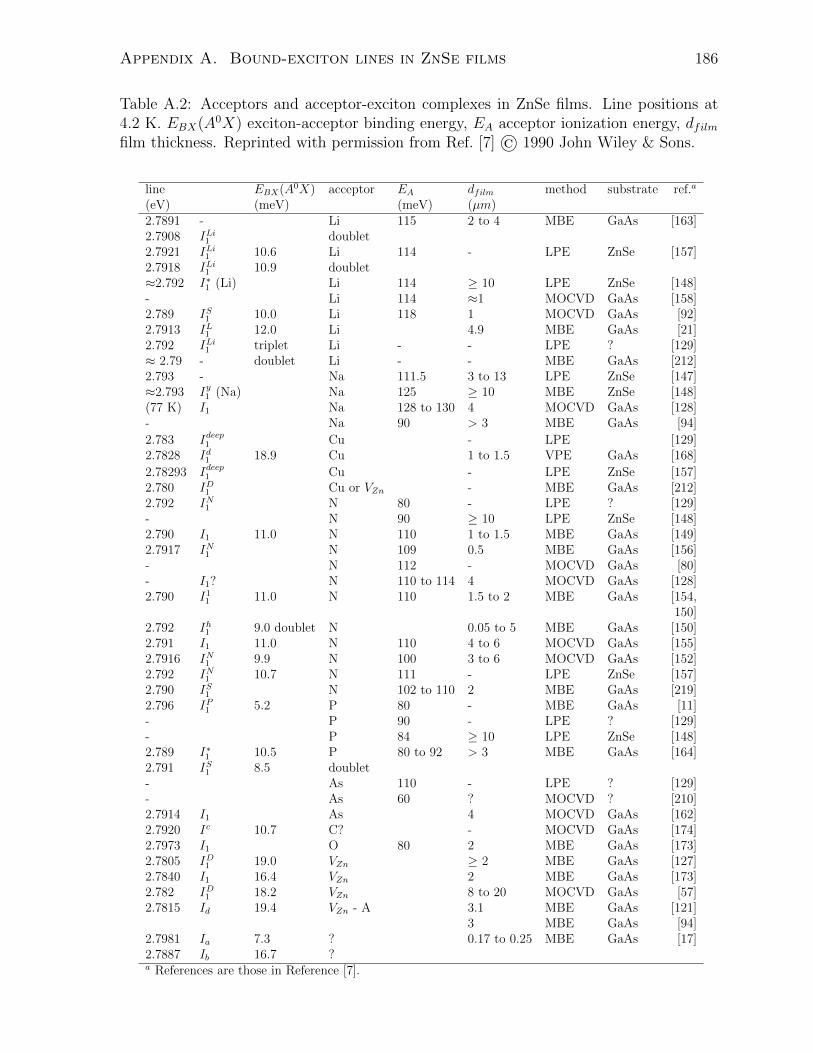
Appendix A. Bound-exciton lines in ZnSe films 186
Table A.2: Acceptors and acceptor-exciton complexes in ZnSe films. Line positions at4.2 K. EBX(A0X) exciton-acceptor binding energy, EA acceptor ionization energy, dfilmfilm thickness. Reprinted with permission from Ref. [7] © 1990 John Wiley & Sons.
line EBX(A0X) acceptor EA dfilm method substrate ref.a
(eV) (meV) (meV) (µm)2.7891 - Li 115 2 to 4 MBE GaAs [163]2.7908 ILi1 doublet2.7921 ILi1 10.6 Li 114 - LPE ZnSe [157]2.7918 ILi1 10.9 doublet≈2.792 I∗1 (Li) Li 114 ≥ 10 LPE ZnSe [148]- Li 114 ≈1 MOCVD GaAs [158]2.789 IS1 10.0 Li 118 1 MOCVD GaAs [92]2.7913 IL1 12.0 Li 4.9 MBE GaAs [21]2.792 ILi1 triplet Li - - LPE ? [129]≈ 2.79 - doublet Li - - MBE GaAs [212]2.793 - Na 111.5 3 to 13 LPE ZnSe [147]≈2.793 Iy1 (Na) Na 125 ≥ 10 MBE ZnSe [148](77 K) I1 Na 128 to 130 4 MOCVD GaAs [128]- Na 90 > 3 MBE GaAs [94]
2.783 Ideep1 Cu - LPE [129]2.7828 Id1 18.9 Cu 1 to 1.5 VPE GaAs [168]
2.78293 Ideep1 Cu - LPE ZnSe [157]2.780 ID1 Cu or VZn - MBE GaAs [212]2.792 IN1 N 80 - LPE ? [129]- N 90 ≥ 10 LPE ZnSe [148]2.790 I1 11.0 N 110 1 to 1.5 MBE GaAs [149]2.7917 IN1 N 109 0.5 MBE GaAs [156]- N 112 - MOCVD GaAs [80]- I1? N 110 to 114 4 MOCVD GaAs [128]2.790 I11 11.0 N 110 1.5 to 2 MBE GaAs [154,
150]2.792 Ih1 9.0 doublet N 0.05 to 5 MBE GaAs [150]2.791 I1 11.0 N 110 4 to 6 MOCVD GaAs [155]2.7916 IN1 9.9 N 100 3 to 6 MOCVD GaAs [152]2.792 IN1 10.7 N 111 - LPE ZnSe [157]2.790 IS1 N 102 to 110 2 MBE GaAs [219]2.796 IP1 5.2 P 80 - MBE GaAs [11]- P 90 - LPE ? [129]- P 84 ≥ 10 LPE ZnSe [148]2.789 I∗1 10.5 P 80 to 92 > 3 MBE GaAs [164]2.791 IS1 8.5 doublet- As 110 - LPE ? [129]- As 60 ? MOCVD ? [210]2.7914 I1 As 4 MOCVD GaAs [162]2.7920 Ic 10.7 C? - MOCVD GaAs [174]2.7973 I1 O 80 2 MBE GaAs [173]2.7805 ID1 19.0 VZn ≥ 2 MBE GaAs [127]2.7840 I1 16.4 VZn 2 MBE GaAs [173]2.782 ID1 18.2 VZn 8 to 20 MOCVD GaAs [57]2.7815 Id 19.4 VZn - A 3.1 MBE GaAs [121]
3 MBE GaAs [94]2.7981 Ia 7.3 ? 0.17 to 0.25 MBE GaAs [17]2.7887 Ib 16.7 ?a References are those in Reference [7].
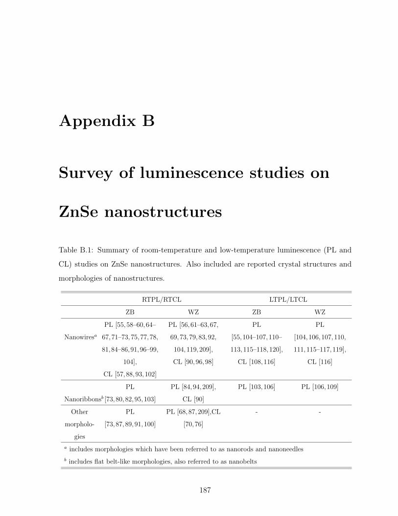
Appendix B
Survey of luminescence studies on
ZnSe nanostructures
Table B.1: Summary of room-temperature and low-temperature luminescence (PL and
CL) studies on ZnSe nanostructures. Also included are reported crystal structures and
morphologies of nanostructures.
RTPL/RTCL LTPL/LTCL
ZB WZ ZB WZ
Nanowiresa
PL [55,58–60,64–
67,71–73,75,77,78,
81,84–86,91,96–99,
104],
CL [57,88,93,102]
PL [56,61–63,67,
69,73,79,83,92,
104,119,209],
CL [90,96,98]
PL
[55,104–107,110–
113,115–118,120],
CL [108,116]
PL
[104,106,107,110,
111,115–117,119],
CL [116]
Nanoribbonsb
PL
[73,80,82,95,103]
PL [84,94,209],
CL [90]
PL [103,106] PL [106,109]
Other
morpholo-
gies
PL
[73,87,89,91,100]
PL [68,87,209],CL
[70,76]
- -
a includes morphologies which have been referred to as nanorods and nanoneedles
b includes flat belt-like morphologies, also referred to as nanobelts
187

Appendix B. Literature survey 188
Table B.2: Summary of energy positions of the near band-edge (NBE) peak and deep-level
(DL) emission band reported for ZnSe nanostructures using their RTPL characterization.
NBE peak Reference(s) DL emission band Reference(s)
energy (ENBE (eV)) energy (EDL (eV))
ENBE < 2.5 [86] EDL < 1.9 [57,64]
2.5 ≤ ENBE < 2.6 -
2.6 ≤ ENBE < 2.7 [57,59,63–66,68,72,
77,81,82,84–86,91,
93,96,100,102,103]
1.9 ≤ EDL < 2.2 [56,61,63,65,66,
68,70,72,73,76,
78,92–97,102,104,
119]2.7 ≤ ENBE < 2.8 [56,58,60,70,73,73,
76,83,86,88,104,
119,209]
2.8 ≤ ENBE < 3.0 [63,69,73,75,79,83,
86,87,90,95,96,98,
99,101,209]
2.2 ≤ EDL [55, 59,64,69,70,
72,73,79,80,82,
83,86,88,96,99–
102,209]3.0 ≤ ENBE [62, 79,92,98]
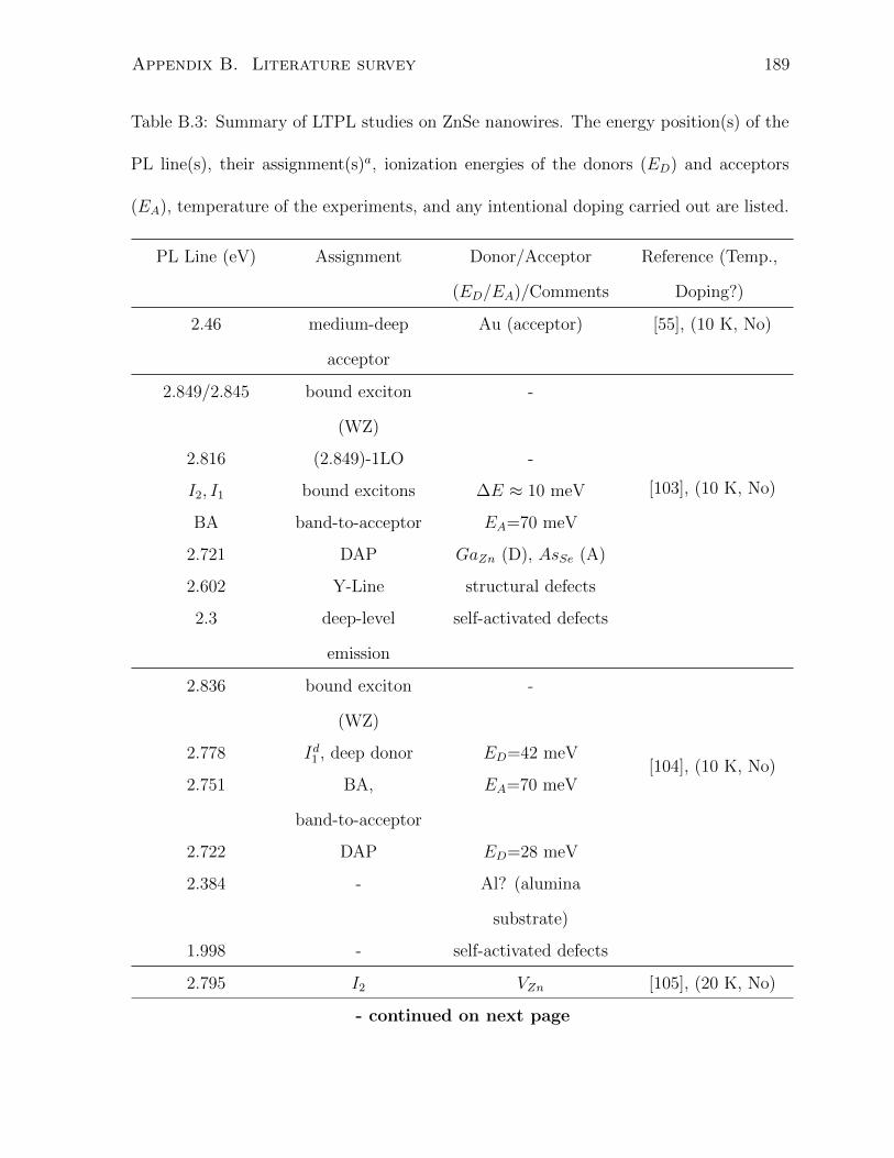
Appendix B. Literature survey 189
Table B.3: Summary of LTPL studies on ZnSe nanowires. The energy position(s) of the
PL line(s), their assignment(s)a, ionization energies of the donors (ED) and acceptors
(EA), temperature of the experiments, and any intentional doping carried out are listed.
PL Line (eV) Assignment Donor/Acceptor
(ED/EA)/Comments
Reference (Temp.,
Doping?)
2.46 medium-deep
acceptor
Au (acceptor) [55], (10 K, No)
2.849/2.845 bound exciton
(WZ)
-
[103], (10 K, No)
2.816 (2.849)-1LO -
I2, I1 bound excitons ∆E ≈ 10 meV
BA band-to-acceptor EA=70 meV
2.721 DAP GaZn (D), AsSe (A)
2.602 Y-Line structural defects
2.3 deep-level
emission
self-activated defects
2.836 bound exciton
(WZ)
-
[104], (10 K, No)2.778 Id1 , deep donor ED=42 meV
2.751 BA,
band-to-acceptor
EA=70 meV
2.722 DAP ED=28 meV
2.384 - Al? (alumina
substrate)
1.998 - self-activated defects
2.795 I2 VZn [105], (20 K, No)
- continued on next page
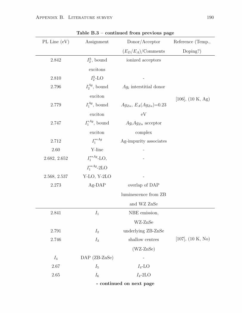
Appendix B. Literature survey 190
Table B.3 – continued from previous page
PL Line (eV) Assignment Donor/Acceptor
(ED/EA)/Comments
Reference (Temp.,
Doping?)
2.842 Ih2 , bound
excitons
ionized acceptors
[106], (10 K, Ag)
2.810 Ih2 -LO -
2.796 IAg2 , bound
exciton
Agi interstitial donor
2.779 IAg1 , bound
exciton
AgZn, EA(AgZn)=0.23
eV
2.747 I∗Ag1 , bound
exciton
AgiAgZn acceptor
complex
2.712 I∗∗Ag1 Ag-impurity associates
2.60 Y-line -
2.682, 2.652 I∗∗Ag1 -LO,
I∗∗Ag1 -2LO
-
2.568, 2.537 Y-LO, Y-2LO -
2.273 Ag-DAP overlap of DAP
luminescence from ZB
and WZ ZnSe
2.841 I1 NBE emission,
WZ-ZnSe
[107], (10 K, No)
2.791 I2 underlying ZB-ZnSe
2.746 I3 shallow centres
(WZ-ZnSe)
I4 DAP (ZB-ZnSe) -
2.67 I5 I4-LO
2.65 I6 I4-2LO
- continued on next page

Appendix B. Literature survey 191
Table B.3 – continued from previous page
PL Line (eV) Assignment Donor/Acceptor
(ED/EA)/Comments
Reference (Temp.,
Doping?)
2.61 I7 I4-3LO
2.783 EHP electron-hole plasma,
∆E=40 meV[108], (4.5 K, No)
2.683 DAP GaZn (D), AsSe (A)
2.2 DL1 deep-level emission
1.95 DL2 deep-level emission
2.806 I2 bound exciton
[109], (10 K, No)
2.792 I1 free exciton
2.762 - band-to-acceptor
2.705 - DAP
2.675, 2.645,
2.615
DAP-LO,
DAP-2LO,
DAP-3LO
-
2.3-2.4 green band vacancies of Zn in
ZnSe
2.48-2.07 - excitons located at
stacking faults[110], (4-5 K, No)
- CdSe quantum dots in
ZnSe nanowires
2.638 - DAP and their
phonon replicas from
residual impurities
[111], (4-5 K, No)
- continued on next page

Appendix B. Literature survey 192
Table B.3 – continued from previous page
PL Line (eV) Assignment Donor/Acceptor
(ED/EA)/Comments
Reference (Temp.,
Doping?)
2.48-2.07 - excitons localized at
the defect zones in
NW
2.794 A neutral donor bound
exciton, VSe
[112], (3.1 K, No)2.714 B DAP, ED=27±1 meV,
EA=102 meV
2.686 C DAP, ED=27±1 meV,
EA=139 meV
2.603 D Y0 line
2.580 E Y0-LO
2.68 - DAP, Na doping
[113], (10 K, No)2.27 - deep-level, Cu doping
1.95 - deep-level,
self-activated peak
2.818 band-edge bulk ZnSe
[115], 5 K, No2.48-2.76 - -
2.07-2.48 - excitons localized at
the defect zones in
nanoneedles
- CdSe quantum dots in
ZnSe nanowires
2.48-2.76 - bunch of spectral lines
[116], (5 K, No)2.07-2.48 - excitons localized at
the defect zones
- continued on next page

Appendix B. Literature survey 193
Table B.3 – continued from previous page
PL Line (eV) Assignment Donor/Acceptor
(ED/EA)/Comments
Reference (Temp.,
Doping?)
- CdSe quantum dots in
ZnSe nanowires
2.655 - exciton-related
luminescence[117], (20 K, No)
2.60 - red-shifted due to
poor crystal quality
2.655 - shallow donor
deep-acceptor pairs,
∆E=165 meV
[118], (20 K, No)
2.8 Ex free exciton
[119], (10 K, P)2.787 IS1 acceptor-bound
exciton, P acceptor,
EA0X=13 meV,
EA=130 meV
- I2 neutral donor-bound
exciton
2.791 P1 shallow donor (Ga)
[120], (10 K, Ga, Ag)2.778 P2 AgZn acceptor
complex
2.700 - DAP
a notation of PL lines, being author-specific, are not included in the List of Symbols
Appendix C
Photoluminescence (PL)
Spectroscopy
C.1 Principles
Photoluminescence (PL) is a spectroscopic technique used for the characterization of
both intrinsic and extrinsic properties of a semiconductor. PL is the luminescence from
a semiconductor when it is excited by light (photo-excitation). When a semiconductor
absorbs a photon of light with energy greater than the Eg (or in the case of resonant
excitation, equal to the Eg) of the semiconductor, an electron is excited to the conduc-
tion band leaving behind a hole (empty electron site) in the valence band. It is to be
noted that Eg refers to the energy band gap at the measurement temperature. The
electron in the conduction band and hole in the valence band are collectively referred
to as an electron-hole pair. The electron and hole, although may be created above the
band minima, relax into a quasi-equilibrium distribution to the bottom of the conduction
band and to the top of the valence band, respectively, via fast phonon-assisted processes
followed by their radiative recombination emitting light of photon energy equal to Eg.
194

Appendix C. PL spectroscopy 195
This process involving free electrons and holes is also referred to as the ‘band-to-band
radiative recombination’ or ’free-carrier recombination’ in a direct Eg semiconductor. In
an indirect Eg semiconductor, where the conduction and valence band edges are sepa-
rated from each other in the momentum (k) space, a phonon must participate in the
recombination process to conserve momentum, and this recombination is called ‘indirect
transition’. An electron-hole pair can also recombine non-radiatively in a so-called non-
radiative recombination, where phonons are emitted instead of photons. Note that both
photons and phonons are emitted in some transitions. PL spectroscopy essentially in-
volves a study of the energy dependence (spectral distribution) of the number of photons
emitted (related to the intensity of PL) during radiative transitions. The features of a PL
spectrum, such as its intensity and spectral distribution, are closely related to the elec-
tronic states of the luminescent centres involved, and can be used to identify them. The
radiative transitions observed in a PL spectrum can be distinguished as intrinsic (band-
to-band), extrinsic (impurity-related) and excitonic. The band-to-band recombination
is the simplest of a variety of pathways (or channels) for the radiative recombination of
electron-hole pairs. A common feature to these different pathways is that the electrons in
the material move into the allowed excited states after photo-excitation. These discrete
energy states between the band edges are often introduced by the impurities and/or na-
tive defects present in semiconductors. The electrons return to their equilibrium states
via radiative or non-radiative transitions. In case of radiative transitions, the energy
of the emitted photons is related to the difference in the energy levels between the two
electron states involved in the transition, i.e. between the excited and the equilibrium
states. Figure C.1 (a) shows a simplified energy band diagram showing most commonly
observed energy levels in a semiconductor, relative to the conduction and valence band
edges. The other recombination channels are discussed below, assuming an above Eg
excitation. These are also shown in Figure C.1 (b).
Free-excitons
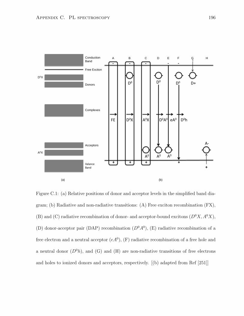
Appendix C. PL spectroscopy 196
- - -
+ + +
A0 A0 A0
+ +
Conduction
Band
Free Exciton
Donors
Valance Band
Acceptors
A0X
D0X
(a) (b)
A-
D0 D0 D0 D+
A B C D E F G H
- - -
Complexes
D0h eA0 D0A0 A0X D0X FE
Figure C.1: (a) Relative positions of donor and acceptor levels in the simplified band dia-
gram; (b) Radiative and non-radiative transitions: (A) Free exciton recombination (FX),
(B) and (C) radiative recombination of donor- and acceptor-bound excitons (D0X,A0X),
(D) donor-acceptor pair (DAP) recombination (D0A0), (E) radiative recombination of a
free electron and a neutral acceptor (eA0), (F) radiative recombination of a free hole and
a neutral donor (D0h), and (G) and (H) are non-radiative transitions of free electrons
and holes to ionized donors and acceptors, respectively. [(b) adapted from Ref [251]]

Appendix C. PL spectroscopy 197
At low temperatures in a reasonably pure semiconductor, the photo-excited electron
and hole are bound by Coulomb interaction, and the electron-hole pair is then called
an exciton. Excitons are usually classified into: Frenkel excitons and Wannier excitons,
distinguished by the length scale of interaction between electron and hole. The Frenkel
exciton is tightly bound and highly localized, and the distance between an electron and
a hole is about few angstroms. These excitons have a large binding energy and are
typically found in insulators and organic materials. The Wannier exciton on the other
hand, has a small binding energy with the electron-hole separation of the order of 10-
100 A. The Wannier excitons are often found in inorganic materials, and move freely in
the material. Since the excitons in ZnSe are Wannier excitons, the following discussion
related to excitons pertains to Wannier excitons.
If the exciton is not localized about an impurity or defect site in the lattice, it is free
to move in the crystal lattice and is called a free exciton. Free excitons form a series
of separated states near the conduction band-edge, and the emission energy from these
states is given by:
hνFX = Eg − EFX (C.1)
where EFX is the binding energy or the energy states of the free exciton associated with
the Coulomb interaction in the presence of crystal potential and hνFX is the emission
energy corresponding to the free exciton emission. The binding energy of the free exciton
is taken relative to the conduction band. In an exciton, the electron orbits the hole
similar to the electron in a hydrogen atom, thus a hydrogenic model is used to calculate
their binding energy. According to the hydrogenic model for an interacting positive and
negative charge, the binding energy of the free excitons is described as:
EFX =1
n2FX
m∗re4
2~2ε2(C.2)
where ε is the dielectric constant, ~ the reduced Planck’s constant (=h/2π, where h is
the Planck’s constant) and e is the electronic charge. The integer nFX is the exciton

Appendix C. PL spectroscopy 198
principal quantum number. The ground state of the free exciton corresponds to n=1 in
the Equation C.2. The reduced effective mass of the exciton, m∗r, is given by
1
m∗r=
1
m∗e+
1
m∗h(C.3)
where m∗e is the electron effective mass and m∗h is the hole effective mass. The excitonic
emission spectrum is expected to be like a δ-function, or if the exciton life-time broadening
is included, like a Lorentzian. This is unlike the other recombination transitions which
result in broader emission spectra.
Bound excitons
In a typical semiconductor material, point defects (intrinsic and extrinsic) exist which act
as donors or acceptors (neutral or charged). The shallow donor impurity levels lie in the
energy gap, slightly below the conduction band, see Figure C.1 (a). When these donors
are ionized, their electrons are excited into the conduction band. Similarly, the shallow
acceptor levels lie in the energy gap, just above the edge of the valence band. An electron
is excited from the valence band to the acceptor level when an acceptor is ionized. The
free excitons can be trapped at the sites of these defects via dipole-dipole interactions
(in the case of neutral defects) or dipole-monopole interactions (charged defects). This
trapping of excitons at defect sites is referred to as the binding of excitons resulting in
bound exciton complex(es) (BEC). The excitons in such cases are referred to as bound
excitons, and these may be of the following types:
1. Exciton bound to a neutral donor (D0X): � (⊕)
2. Exciton bound to an ionized donor (D+X): �(⊕)
3. Exciton bound to a neutral acceptor (A0X): ⊕� (⊕)
4. Exciton bound to an ionized acceptor (A−X): �(⊕)
where � and � represent the ionized donor and acceptor, respectively, and and ⊕
are the electron and hole, respectively. An excitons is shown as (⊕). The (D0X)

Appendix C. PL spectroscopy 199
bound exciton is considered to consist of a donor ion, two electrons and a hole whereas
(D+X) complex consists of a donor ion, an electron and a hole. A similar argument holds
for acceptor-bound excitons (A0X) and (A−X). Note that an ionized acceptor usually
does not bind an exciton since a neutral acceptor and a free electron are energetically
more favourable. This is because the hole mass is usually considerably larger than the
reduced mass of an electron and a hole. The bound excitons give PL emission at slightly
lower energies than the free exciton transitions, with narrower linewidths due to their
increased spatial localization. This is because the bound excitons are spatially localized
at the defect sites, and are not free to move in the crystal. This results in their much
smaller kinetic energy compared to free-excitons. The emission from bound excitons has
a much narrower linewidth (� kBT ) than that of the free exciton (∼ kBT ). Here, kB
is the Boltzmann constant and T is the temperature. The emission energy, or the peak
position in PL spectrum for a bound exciton emission, hνBE, is:
hνBE = Eg − EFX − EBX (C.4)
where EBX is the binding energy of the exciton to the impurity or defect. The peak energy
(hνBE) is specific to a given impurity or defects and its charge state in a semiconductor,
and this is the basis for the identification of impurities and defects in a semiconductor
through PL. The ionization energy of shallow donors, ED, and acceptors, EA, according
to the hydrogenic model are given by:
ED = (m∗ee4/2~2ε2) (C.5)
EA = (m∗he4/2~2ε2) (C.6)
Donor-acceptor pair
Both donor and acceptor impurities typically exist in a semiconductor material. When
such a material is irradiated with light, the photo-generated electron-hole pairs neutralize
the shallow ionized donors and acceptors in the material. This may be represented as

Appendix C. PL spectroscopy 200
e− + D+ → D0 and h+ + A− → A0. An electron bound to a donor can recombine with
a hole bound to an acceptor, giving rise to a donor-acceptor pair (DAP) emission.
D0 + A0 → D+ + A− + hνDAP (C.7)
In low-temperature PL from DAP recombinations, the recombination energy is given
by [312]:
EDAP (r) = Eg − (EA + ED) +e2
εr−(e2
ε
)(avdWr
)6
(C.8)
where avdW is the effective van der Waals coefficient for the interaction between a neutral
donor and a neutral acceptor. The term (e2/ε)(avdW/r)6 in Equation C.8 takes into
account the closer separations between the pairs, but is somewhat empirical [313], and
negligible for distant pairs. The term (e2/εr) is the energy due to the Coulomb attraction
between the ionized donor and acceptor. For sufficiently distant pairs, Equation C.8 for
the energy of the emitted photon EDAP (r) reduces to [254]:
EDAP (r) = Eg − (EA + ED) +e2
εr(C.9)
The emission energy of a DAP recombination is therefore a function of the separation
r between the donor and acceptor in a donor-acceptor pair (also referred to simply as
pair). Pair recombination often has a series of distinct but closely packed sharp lines
corresponding to different allowed discrete values of r. These discrete values of r arise
because donors and acceptors must be at the lattice sites, and therefore only r values
permitted by the crystal symmetry are allowed. In some cases, this series of lines results
in a broad band [237].
Free-to-bound
Apart from the band-to-band, excitonic and DAP transitions, there is another type of
transition referred to as free-to-bound (FB) transitions, so called because they involve
a free carrier in the conduction or the valence band, and a bound hole or electron. A
Appendix C. PL spectroscopy 201
free-to-bound or donor-to-hole (D0h) is a recombination of an electron bound to a neutral
donor with a hole in the valence band. The corresponding transition energy for (D0h)
transition is given by:
ED0h = Eg − ED (C.10)
Similarly, an electron from the conduction band recombining with a hole bound to a neu-
ral acceptor is an electron-to-acceptor (eA0) (or bound-to-free) transition, whose transi-
tion energy is:
EeA0 = Eg − EA + kBT (C.11)
where and the last term (kBT ) accounts for the electron kinetic energy. As the temper-
ature increases, the DAP band evolves to a free-to-bound transition. This is due to the
thermal ionization of the shallow impurity and therefore an increase in the free carrier
concentration. Figure C.1 (b) shows the transitions described above schematically (A-F).
Figure C.1 (b) also includes the non-radiative transitions from free electrons and holes
to ionized donors (G) and acceptors (H), respectively.
Phonons are the quantized modes of lattice vibrations due to the vibrations of atoms
forming the crystal. In crystals with more than one kind of atoms, these are of two types:
acoustic and optical. The acoustic modes result when nearby atoms in a crystal vibrate
in the same direction with a periodically varying amplitude. These are similar to sound
waves, and hence the name acoustic. The optical phonons are modes when nearby atoms
vibrate in opposite directions. Each of these are of further two types. The phonons with
atomic displacements parallel to the direction of propagation are longitudinal phonons,
while those with displacements perpendicular to the direction of propagation are trans-
verse phonons. When a PL transition is accompanied by a simultaneous emission of
phonons, subsidiary peaks appear in the PL spectrum on the lower energy side of the
this transition, also referred to as the main transition. These peaks on the lower en-
ergy side are referred to as phonon-replicas, whose energy is lower than that of the
main transition by an energy equal to the phonon energy. For example, in the case of

Appendix C. PL spectroscopy 202
longitudinal-optical (LO) phonon-replicas of the free exciton emission, the energy of the
main transition and its phonon-replicas is given by:
hνFX,m = Eg − EFX −m~ωLO (C.12)
where integer m is the order of the LO-phonon-replica, and ~ωLO is the LO-phonon
energy. hνFX,m is the energy position of the PL peak corresponding to the m-th or-
der LO-phonon replica. hνFX is the transition energy of the zero-phonon line (ZPL)
corresponding to m=0. Similarly, in case of bound exciton emission accompanied by
LO-phonon emission, Equation C.4 becomes:
hνBE,m = Eg − EFX − EBX −m~ωLO (C.13)
C.2 Theoretical models
One of the disadvantages of using PL spectroscopy is that it is a semi-quantitative char-
acterization technique. In order to extract quantitative information from the PL spectra,
the dependence of PL with different varying quantities (typically excitation intensity
(Iexc) and temperature (T )) is used. The simple theoretical models commonly used to
obtain information on recombination mechanisms through the use of these varying quan-
tities are described below.
C.2.1 Excitation intensity dependence of PL
The dependence of the PL spectrum from a semiconductor material on Iexc can be used to
identify the recombination processes involved, and to calculate the ionization energies of
the donors and acceptors involved in DAP-related transitions. The change in integrated
PL intensity (IPL) with Iexc yields information about the type of the optical transition
(e.g. excitonic versus DAP-related), whereas the variation in peak energy with Iexc for

Appendix C. PL spectroscopy 203
a DAP type transition provides information about the ionization energies of the donor
and acceptors involved, introduced by the impurities (extrinsic and intrinsic) and native
point defects. These models are discussed next.
Dependence of IPL on Iexc
As the Iexc is changed, the IPL of the PL peak reflects this change which is usually
characteristic of the type of the transition mechanism involved for a particular emission.
In order to elucidate the dependence of IPL on Iexc, Schmidt et al. [251] solved a set of
rate equations for different recombinations including (A) free-exciton (FX), (B) donor-
bound excitons (D0X), (C) acceptor-bound excitons (A0X), (D) DAP, (E) free electron
to a neutral acceptor, (F) free hole to a neutral donor and (G) non-radiative transitions
of free electrons and hole to neutral donors and acceptors respectively. These transitions
(A)-(H) are shown schematically in the Figure C.1 (b). These rate equations are listed
below, and their solution is described in the work of Schmidt et al. [251].
dn
dt= i′L− a′n2 − g′n(ND −ND0)− e′nNA0 (C.14)
dnFEdt
= a′n2 + j′L−[
1
τFE+
1
τnrFE
]nFE − b′nFEND0 − c′nFENA0 , (C.15)
dnDXdt
= b′nFEND0 −[
1
τDX+
1
τnrDX
]nDX , (C.16)
dnAXdt
= c′nFENA0 −[
1
τAX+
1
τnrAX
]nAX , (C.17)
dNA0
dt= h′(NA −NA0)n+ i′(NA −NA0)L− c′nFENA0 +
[1
τAX+
1
τnrAX
]nAX
−d′ND0NA0 , (C.18)
dND0
dt= g′(ND −ND0)n− k′ND0L− b′nFEND0 +
[1
τDX+
1
τnrDX
]nDX
−d′ND0NA0 − f ′ND0n (C.19)
The symbols are as follows: ND (NA) are the concentrations of donors (acceptors),
ND0 (NA0) are the concentrations of neutral donors (acceptors), the radiative and non-

Appendix C. PL spectroscopy 204
radiative lifetimes of free excitons (τFX and τnrFX), donor-bound excitons (τDX and τnrDX),
and acceptor-bound excitons (τAX and τnrAX). nFE and nDX (nAX) are the concentra-
tions of free and donor-bound (acceptor-bound) excitons, respectively. The coefficients
a′, b′, ..., h′ are the transitions rates of the processes (A-H) indicated in Figure C.1 (b).
The coefficients i′, ...l′ are the transition rates of the following processes: (I) photo-
excitation of the electron-hole pairs by light with photon energy greater than Eg, (J)
formation of the free excitons resonantly by light with photon energy ≈Eg and excitation
of electrons from (K) neutral donors and (L) ionized acceptors by the excitation light,
respectively.
These rate equations were analytic solved using assumptions on excitation, and radia-
tive and non-radiative recombination channels [251]. Schmidt et al. [251] mathematically
expressed the dependence of IPL on Iexc by a power law relation:
IPL ∝ Ipexc (C.20)
The variation of IPL with Iexc can therefore be used to identify the underlying recombi-
nation processes. While this relation can be used to distinguish excitonic emission from
other types, it fails to separate free-to-bound and DAP transitions.
Dependence of peak energy on Iexc
As discussed above, in low-temperature PL from donor-acceptor pair recombinations,
and for sufficiently distant pairs, the energy of the emitted photon EDAP (r) is given by
Equation C.9 [254]. A model was proposed by Zacks and Halperin [237] that described
the dependence of the emission peak energy on Iexc. In their derivation, it was assumed
that the temperature of the semiconductor material is low enough so that the thermal
ionization of donors and acceptors can be neglected. It was also assumed that all photo-
excited electron-hole pairs are captured by ionized impurities, which then become neutral.

Appendix C. PL spectroscopy 205
The model proposed by them is expressed as [237]:
Iexc = Iexc,0(hνm − hν∞)3
hνB + hν∞ − 2hνmexp
(− 2(hνB − hν∞)
hνm − hν∞
)(C.21)
where hνm(= Em) is the emission band peak energy, hν∞(= Eg − (EA + ED)) is the
photon energy corresponding to infinitely distant donor-acceptor pair, hνB(= Eg−(EA+
ED) + e2/εRB) is the emitted photon energy of a donor-acceptor pair separated by a
shallow impurity Bohr radius (RB), and Iexc,0 is a constant of proportionality. A non-
linear least square fit to the experimental data is used to determine the values of hν∞,
hνB and Iexc,0. The change in peak energy with increasing Iexc can be understood by
considering that as the Iexc is increased, closely-lying donor-acceptor pairs are favoured,
and the transition energy moves to higher energy according to Equation C.9.
C.2.2 Temperature dependence of PL
The variation in PL characteristics with a change in temperature provides important
information about the radiative and non-radiative recombination mechanisms involved.
It has been experimentally observed that as the temperature is increased: (i) the spectral
peak position shifts to lower energies, (ii) the PL peak broadens, and (iii) the integrated
intensity of the PL peak reduces. These have been explained using models as discussed
below.
Dependence of peak energy on T
The red-shift in PL peaks with increasing temperatures is mainly linked to the shrinkage
of the Eg at higher temperatures. The temperature dependence of Eg is most commonly
described by a semi-empirical equation proposed by Varshni [262]:
Eg(T ) = Eg(0)− αT 2
β + T(C.22)
where Eg is the direct or indirect energy band gap, Eg(0) is the value of Eg at 0 K and α
and β are the fitting parameters characteristic of a given material. α can be considered
Appendix C. PL spectroscopy 206
to be the temperature gradient (dEg/dT ) at high temperatures, and β to be proportional
to the Debye temperature θD for the material. This equation was proposed based on the
two experimental facts that the change in the relative positions of the conduction and
valence bands (which determine the Eg):
1. due to thermal expansion of the crystal lattice is linear at high temperatures and
non-linear in the low-temperature regime. This change in the Eg due to the ex-
pansion of the lattice however only accounts for a quarter of the total change in Eg
with the temperature.
2. due to the electron-lattice interactions is quadratic for T � θD and linear for T �
θD. A major contribution to the total change in the Eg is due to this interaction.
This equation was fit to the data available for Eg at different temperatures for several
materials [262], and the fit was found to be satisfactory. Despite being a widely used
equation to describe the change in Eg with temperature, its weak theoretical basis is
also acknowledged [314]. Another expression with a more microscopic basis, but still
semi-empirical, to model this dependence has also been in use and expressed as [315]:
Eg(T ) = Eg(0)− 2αB[exp
(θBT
)− 1
] (C.23)
where αB is the strength of the exciton-average phonon interaction, and θB is a temper-
ature corresponding to an average phonon energy. This model takes into account the
Bose-Einstein statistical factor NLO (=1/[exp(θLO/T )− 1]) for the phonon emission and
absorption, where θLO is the temperature corresponding to the LO-phonon energy. This
model is based on the consideration that both acoustic and optical phonons contribute
to the red-shift of the Eg via electron-lattice interactions. Note that the Equations C.22
and C.23 describe the dependence of only Eg on temperature, and not necessarily the
dependence of PL peak positions in a PL spectrum corresponding to different processes
on temperature. Since the FX emission follows the Eg for a wide temperature range,
Appendix C. PL spectroscopy 207
the parameters obtained from the fits of FX emission peak position with temperature to
these equations are representative of the dependence of Eg on temperature. For the PL
peaks related to bound excitons these parameters can be, and usually are, different from
those for the FX emission and Eg.
Dependence of HWHM on T
The dependence of linewidths (Γp) of exciton lines on temperature provides important
information about the exciton-phonon interactions and exciton-impurity scattering. The
Γp of an excitonic line in PL from a semiconductor includes contributions from homo-
geneous and inhomogeneous broadening. The temperature dependence of the excitonic
linewidths (in terms of the HWHM, Γp/2) in semiconductors is represented as a sum of
different contributions to it,
Γp(T )/2 = Γinh + γthT +ΓLO[
exp
(θLO
T
)− 1
] + Γimp exp(−Eimp/kBT ) (C.24)
where each term on the right side of the expression is discussed next. Γinh is a tem-
perature independent inhomogeneous broadening contribution term which includes the
effects of intrinsic lifetimes, carrier-carrier scattering, surface scattering as well as those
of instrumental broadening. The most common mechanism that contributes to the ho-
mogeneous broadening of the Γp is due to the process of phonon scattering. This implies
the collisions of excitons with phonons which result in their dissociation, and both acous-
tic and optical phonons are involved in these scattering processes. The contributions of
acoustic and optical phonons to the homogeneous broadening of Γp are proportional to
their respective population density. In the low temperature range, the density of acoustic
phonons is relatively high and acoustic-phonon scattering dominates. This is represented
by the second term in the Equation C.24, and γth represents the strength of the exciton-
acoustic phonon coupling. The population of optical phonons follows the Bose-Einstein
statistical factor (NLO) and becomes significant at higher temperatures. The third term
Appendix C. PL spectroscopy 208
represents the homogeneous broadening due to exciton-optical phonon scattering, and
ΓLO is the strength of exciton-optical phonon coupling. The last term in Equation C.24
represents the inhomogeneous broadening due to scattering by ionized impurities, and
proportional to the density of ionized impurity scattering centres. Γimp is contribution to
Γp due to scattering by fully ionized impurities, and Eimp is the average binding energy
of the impurities. The experimentally obtained values of the Γp at different temperatuers
is fit to the Equation C.24, and relevant parameters are obtained. It is to be noted that
the last term in Equation C.24 (exciton-ionized impurity scattering process) is usually
neglected because of its negligible contribution. The resulting equation still contains four
fitting parameters, of which θLO is usually kept fixed as the temperature corresponding
to the LO-phonon energy.
Dependence of IPL on T
The efficiency of PL emission is given by
η =Pr
Pr + Pnr(C.25)
where Pr is temperature independent probability of a radiative transition, and Pnr is the
probability for a non-radiative transition whose dependence on temperature is given by:
Pnr = Pnr,0 exp (−Ea/kBT ) (C.26)
In this equation, Pnr,0 is a temperature independent prefactor, and Ea is the thermal
activation energy which can be understood as the height of a barrier around the re-
combination centre induced by perturbations in the band structure. Only the carriers
with energies similar to or higher than Ea can overcome this barrier and recombine
non-radiatively. The probability of non-radiative transitions therefore increases with the

Appendix C. PL spectroscopy 209
temperature. The PL emission efficiency becomes
η =1
1 + PnrPr
(C.27)
=1
1 +Pnr,0Pr
exp(−Ea/kBT )(C.28)
=1
1 + C exp (−Ea/kBT )(C.29)
where C = Pnr,0/Pr is a coefficient. The dependence of integrated PL intensity (IPL) on
temperature can therefore be expressed as
IPL(T ) =IPL(0)
1 + C exp (−Ea/kBT )(C.30)
The above equations were based on a single thermally activated non-radiative tran-
sition mechanism. For recombinations accompanied by two such mechanisms, the Equa-
tions C.25 to C.30 are modified to:
η =Pr
Pr + Pnr1 + Pnr2(C.31)
Pnr1 = Pnr1,0 exp (−Ea1/kBT ) (C.32)
Pnr2 = Pnr2,0 exp (−Ea2/kBT ) (C.33)
η =1
1 + Pnr1Pr
+ Pnr2Pr
(C.34)
=1
1 +Pnr1,0Pr
exp(−Ea1/kBT ) +Pnr2,0Pr
exp(−Ea2/kBT )(C.35)
=1
1 + C1 exp(−Ea1/kBT ) + C2 exp(−Ea2/kBT )(C.36)
IPL(T ) =IPL(0)
1 + C1 exp(−Ea1/kBT ) + C2 exp(−Ea2/kBT )(C.37)
where subscripts 1 and 2 refer to the two non-radiative recombination mechanisms. Ex-
tension of these equations to include more than two non-radiative transitions are straight-
forward. These thermal activation energies (Ea, Ea1, Ea2) are interpreted in context of

Appendix C. PL spectroscopy 210
the behaviour of the observed peaks with the temperature in the temperature-dependent
PL spectra.

Appendix D
Time-resolved Photoluminescence
(TRPL) spectroscopy
Time-resolved spectroscopy techniques are a powerful means of studying a material giving
information about the nature of the excitation, energy transfer, molecular motion and
molecular environment. Time-resolved photoluminescence (TRPL) spectroscopy is an
extension of the time-integrated (or conventional) PL spectroscopy, and facilitates the
study of the dynamics of photo-excited carriers in a semiconductor. In TRPL, ultra-
short laser pulses excite the semiconductor generating a large number of electrons and
holes, and the resulting luminescence from the semiconductor sample is collected and
dispersed by a spectrometer, and later detected by a detector. The principle is similar
to that of the PL spectroscopy, the main difference being that the laser excitation needs
to be pulsed, and the detection device should have a very fast time response. In the
present case, the experimental setup for TRPL spectroscopy is similar to that for PL
spectroscopy, with the exception that the spectrometer and CCD detector are replaced
by another spectrometer (ACTON PI 300i), and a streak camera (Hamamatsu C5680) is
used for time-resolved detection. This is the excite-and-probe technique for time-resolved
211

Appendix D. TRPL spectroscopy 212
Input slit
Input optics
Trigger signal
Photocathode
Multi-channel
Plate (MCP)
Time
Streak image
Incident
luminescence
signal
Deflection
electrodes
Sweep circuit
Accelerating
electrode Phosphor
screen
Wavelength
Figure D.1: Components and principle of operation of a streak camera
spectroscopy, distinguished from the pump-probe methods of time-resolved spectroscopy.
The main components and the operating principle of streak camera are described next.
The PL intensity can be measured as a function of time after the excitation pulse
was incident on the semiconductor using pulsed excitation. The carrier recombinations
in a semiconductor take place at a very fast rate, typically of the order of pico-seconds
(ps), and conventional detectors having longer response times prove to be inadequate
for measuring such fast photo-responses from the semiconductors. A more sophisticated
detector, called a streak camera is used to measure such short carrier lifetimes. The main
components and the operating principle of a streak camera are shown in Figure D.1.
The photons of the emitted luminescence signal entering the system through the input
slit are converted to electrons by a photocathode. The electrons then travel between two
electrodes to which a time-varying electric field is applied synchronously with the incident
light. The sweep rate of the electric field is varied from zero to a certain maximum value

Appendix D. TRPL spectroscopy 213
with rates as high as 2000 V/ns. The electron are deflected by this electric field, and
during this deflection process, the electrons arriving first are deflected less than the ones
arriving later. The electrons then hit a phosphor screen (or CCD array in some cases)
which is placed on the other side of the electrodes. The electrons arriving first hit the
screen in the top part, while the electrons arriving later hit the bottom part of the screen.
The vertical axis of the mapped image of PL intensity on the phosphor screen, also called
the streak image (since the incoming electrons leave a streak on the phosphor screen), is
thus the time axis. The time-resolution of the streak camera is limited by the sensitivity
of the voltage applied to the electrodes, and this can be as low as 100 V/cm. When
a streak camera is used with a spectrometer, the PL is also spectrally resolved before
entering the detector, and the horizontal axis of the phosphor screen (streak image) then
serves as the wavelength axis. The streak camera is used in conjunction with the delay
generator and trigger for synchronization with the ultra-fast laser. The stated resolution
of the streak camera system is 2 ps. During the TRPL measurements, the PL intensity
is recorded as a function of decay time, and the resulting curve can be fitted to yield the
value(s) of carrier recombination lifetime(s) τ .
Appendix E
Electronic band structures
E.1 Energy band diagrams
In isolated atoms, the allowed energy states of the electrons are discrete. The periodic
potential of the atoms (ion-cores and the bound electrons) in a crystal affects the energy
states of the electrons. The electronic energy bands in solids result from the overlapping
of the orbitals of atoms that form the solid. This overlapping depends on the geometric
arrangement of the atoms (crystal lattice), the difference of energy between the atomic
orbitals in the solid, and the number of valence electrons in the atoms. The energy bands
are the ranges of allowed electron energies when atoms are brought together in forming a
crystal. The ranges with no allowed energies of electrons are the forbidden gaps or band
gaps. The highest energy band which contains electrons at temperatures above absolute
zero is referred to as the conduction band. The valence band is the next lower-lying band,
mostly filled with electrons, and separated from the conduction band by an energy gap
(∼eV) in semiconductors. The wavevector k is related to the direction of motion of an
electron in a crystal. The energy band diagrams, also referred to as E−k plots or energy
dispersion curves or electronic band structures, are the informational plots of allowed
214

Appendix E. Electronic band structures 215
values of the electron energy as a function of k. The combined effect of periodic potential
of atoms in a crystal is incorporated by adjusting the mass of an electron to a different
value, known as the effective mass (m∗). The effective mass is inversely proportional to
the curvature of an E − k curve. The optical, electrical and magnetic properties of a
solid are determined by its electronic band structure.
The k values associated with a given energy band are said to form a Brillouin zone
(BZ). The BZ’s are numbered consecutively beginning with the lowest energy band, which
forms the first BZ. The first BZ of ZB crystal lattices is shown in Figure E.1 (a). It is an
octahedron, truncated by the {100} planes at a distance 2π/a from the zone-centre, where
a is the lattice constant of the ZB crystal. Γ identifies the centre of the first BZ at k=0.
For BZs of other crystal lattices, Γ denotes the zone centre. Other symbols in Figure E.1
(a) denote the points and directions of high symmetry, also called critical points. As a
convention, the points and directions inside the BZ are labelled by Greek letters, while
those on the surface of the BZ by Roman letters. Some of these high-symmetry points,
and the three high-symmetry directions are:
• X denotes the zone-end along the 〈100〉 direction
• L denotes the zone-end along the 〈111〉 direction
• K denotes the zone-end along the 〈110〉 direction
• 〈100〉: Γ→ X is denoted as ∆
• 〈111〉: Γ→ L is denoted as Λ
• 〈110〉: Γ→ K is denoted as Σ
The first BZ for a WZ crystal lattice with hexagonal symmetry is shown in Figure E.1
(b). The critical points in the first BZ of a hexagonal lattice are:
• A denotes the zone-end along the 〈001〉 direction
• M denotes the zone-end along the 〈100〉 direction

Appendix E. Electronic band structures 216
Fig
ure
E.1
:F
irst
BZ
of(a
)Z
Ban
d(b
)W
Zcr
yst
alla
ttic
es[3
16].

Appendix E. Electronic band structures 217
• 〈001〉: Γ→ A is denoted as ∆
• 〈100〉: Γ→ M is denoted as Σ
Figure E.2 shows the electronic structures for ZnSe in the ZB and WZ crystal struc-
tures, calculated using LDA (local density approximation) method [317]. The conduction
band minima (CBM) and valence band maxima (VBM) both occur at k=0.
(a) (b)
Ene
rgy
(eV
)
Figure E.2: Calculated band structures of ZnSe in (a) ZB and (b) WZ crystal structures.
Reprinted with permission from Ref. [317] © 1994 American Physical Society.
E.2 Band structure calculations for Nanowire Twin-
ning Superlattices
Since the NWs and NTSLs in present samples are rather thick with the smallest being 50
nm in diameter, effect of quantum confinement on the electronic structure is negligible.

Appendix E. Electronic band structures 218
Therefore, these structures may be modeled as one-dimensional superlattices. The band
structures of NTSLs were calculated using ab Initio pseudopotentials within the local-
density approximation as implemented in the ABINIT package [318]. Trullier-Martins
pseudopotentials were used that include d-orbitals in the valence states for Zn [319].
Inclusion of d-orbitals increases the computational complexity but is essential for an ac-
curate description of structural properties. The lattice constant for ZB structure was
determined by minimization of the total energy to be 5.531 A which is only 1% smaller
than the experimental value. The geometry for all structures were obtained by stacking
layers with ideal lattice spacing of the ZB structure. For wurzite structure (2H) use of
fully optimized geometry reduces the band-gap by 5 meV. For NH structures with N > 2
deviation from the assumed ideal geomerty is expected to change the band-gap by an
even smaller amount. An energy cutoff of 80 Rydberg was used so that the band gap
energy converged to within a few meV. As is well-known, LDA significantly underesti-
mates the band-gap [320], so for comparison with experiments, a constant scissors shift
of 1.642 eV (chosen to align the bandgap of ZB structure with experiments) was applied
uniformly to all structures [320]. The top of the valence band which is 3-fold degener-
ate in the cubic (ZB) structure splits into two in all other structures. This crystal field
splitting is largest in the WZ (2H) structure with a value of 71 meV gradually decreasing
to zero as N increases. In all cases the band-gap is direct (at k = 0) and with inter-
band transition dipole moments only weakly varying with the periodicity. This is not
surprising as the deviation from ideal ZB structure is small and, to a good approxima-
tion, the band-structure may be viewed as that of the ZB structure folded in k-space as
demanded by the periodicity. Figure E.3 presents the electronic structures obtained from
ab Initio calculations for (a) 2H, (b) 4H (γ=0.5) and (c) 6H (γ=0.333) polytypes of ZnSe
with relevant details given in the figure captions. Figure E.4 compares the calculated
band structures for 2H and 4H polytypes where the reduction in direct band gap for 4H
structure in comparison to that of 2H structure can be noticed.

Appendix E. Electronic band structures 219
-6
-4
-2
0
2
4
A Γ K M G
Ener
gy (e
V)
-6
-4
-2
0
2
4
A Γ K M G
Ener
gy (e
V)
-6
-4
-2
0
2
4
A Γ K M G
Ener
gy (e
V)
a2H
b4H
c6H
VBM
VBM
VBM
Figure E.3: Band-structure of ZnSe
NTSLs calculated using ab Initio pseu-
dopotential method within the local
density approximation (LDA). The en-
ergy bands of the NH structure are
closely related to that of the wurtzite
structure (2H) with bands folded at
2/N(0, 0, 2π/c) along the Γ-A direction.
This can be clearly seen by compar-
ing the band-structures for the 2H (a)
and 4H (b), for example. It is noted
that there are some important devia-
tions such as splitting of some degenera-
cies that cannot be accounted for by a
simple folding. However, the bands near
the direct band gap at the Γ point are
very similar in all the structures apart
from a gradual shift in the band gap
with N . The horizontal line indicates
the position of the valence band max-
imum (VBM). Also shown is the cal-
culated band-structure for 6H-polytype
(c).

Appendix E. Electronic band structures 220
-3
-2
-1
0
1
2
A A1 Γ K
Ener
gy (e
V)
VBM
Figure E.4: Comparison of the calculated band-structures for wurtzite (2H) (red) and
4H-polytype (blue) structures. A and A1 denote the Brillouin zone boundary along the
growth direction for 2H and 4H structures, respectively. The band gap for 4H-poytype
is reduced compared to that of wurtzite (2H) structure. The horizontal line (green)
indicates the position of the valence band maximum (VBM).

Appendix F
Softwares and Programs used
The following softwares and computer programs were used for the acquisition of data,
and their analysis.
• SpectraMax for Windows Version 3.2 (Horiba Scientific) was used to control
the spectrometer (Jobin-Yvon, TRIAX320) and the CCD detector (Jobin-Yvon,
CCD3000). The same program was used to acquire the PL spectra from NWs.
The parameters of acquisition such as ti, dslit and centre wavelength were adjusted
using this program before the acquisition of each PL spectrum. A background
subtraction feature built into this program was used, which automatically subtracts
the background (dark) signal before the acquisition of a PL spectrum.
• HPD-TA (High-Performance Digital Temporal Analyzer) Version 8.4.0 pf5 07.04.2010
(Hamamtsu Photonics Deutschland) was used to acquire TRPL streak images. The
second spectrometer (ACTON PI 300i) and other accessories for the streak cam-
era e.g., the delay generator, were also controlled by this program. The centre
wavelength for the spectrometer, dynamic time range (1-4), delay time, and other
parameters for the acquisition of streak images were controlled using HPD-TA. In
this case, the equivalent of ti is the number of frames to be acquired, which can be
221

Appendix F. Softwares and Programs used 222
adjusted using this program. The slits for both the streak camera and the second
spectrometer were manual, and not adjustable on the program.
• DigitalMicrograph Version 2.02.800.0 (GATAN) was used to acquire the TEM
and HR-TEM microgrpahs on Titan-80-300 (FEI) and JEOL-2010F STEMs. It was
also used for the acquisition of SAD patterns on JEOL-2010F. The FFT patterns
were generated by selecting an area on the HR-TEM micrographs using DigitalMi-
crograph. For the indexing of SAD and FFT patterns, the distances between the
diffraction spots were measured using this program. For counting the number of
monolayers and measuring the widths of the individual segments on TEM and
HR-TEM micrographs from NTSLs, a profile from a selected area was used in
DigitalMicrograph, which displays the intensity of the pixels in the selected area.
• Origin Version 7.0 (OriginLab) was used to analyze the PL spectra. This includes
fitting of the PL spectra to peaks functions, e.g., Lorentzians and Gaussians. The
parameters, e.g., Ep, Γp and IPL obtained from the above fitting were fit to the
theoretical models using the same program. The same program was used to generate
all the PL plots and plots with data i.e., excluding the TEM, HR-TEM micrographs,
SAD patterns and electronic-structure plots, presented in this thesis.
• Others These include:
– ImageJ (Open Source) for image-processing
– MATLAB (MathWorks) for data analysis (in addition to Origin)
– the drivers and accompanying image-acquisition programs for the frame-grabber
boards (Data Translation, DT3120 and 1stVision Inc., PC2Vision) used to
capture images from CCD cameras (Hitachi KP-32N and analog CCD camera
inside the streak camera)
– LibreOffice (Open Source) for labelling the indexed SAD patterns
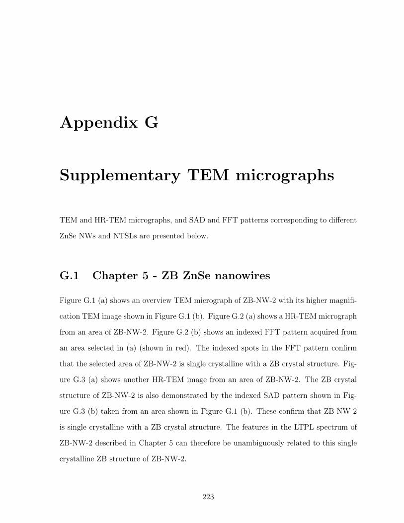
Appendix G
Supplementary TEM micrographs
TEM and HR-TEM micrographs, and SAD and FFT patterns corresponding to different
ZnSe NWs and NTSLs are presented below.
G.1 Chapter 5 - ZB ZnSe nanowires
Figure G.1 (a) shows an overview TEM micrograph of ZB-NW-2 with its higher magnifi-
cation TEM image shown in Figure G.1 (b). Figure G.2 (a) shows a HR-TEM micrograph
from an area of ZB-NW-2. Figure G.2 (b) shows an indexed FFT pattern acquired from
an area selected in (a) (shown in red). The indexed spots in the FFT pattern confirm
that the selected area of ZB-NW-2 is single crystalline with a ZB crystal structure. Fig-
ure G.3 (a) shows another HR-TEM image from an area of ZB-NW-2. The ZB crystal
structure of ZB-NW-2 is also demonstrated by the indexed SAD pattern shown in Fig-
ure G.3 (b) taken from an area shown in Figure G.1 (b). These confirm that ZB-NW-2
is single crystalline with a ZB crystal structure. The features in the LTPL spectrum of
ZB-NW-2 described in Chapter 5 can therefore be unambiguously related to this single
crystalline ZB structure of ZB-NW-2.
223

Appendix G. Supplementary TEM micrographs 224
a b
ZB-NW-2
Location of SAD
Figure G.1: Structural characterization of ZB-NW-2: (a) Overview TEM micrograph,
and (b) TEM micrograph at a magnification higher than in (a).
a b
111
111
220
220
002
002
111
111
Figure G.2: (a) HR-TEM micrograph from an area of ZB-NW-2, and (b) Indexed FFT
pattern acquired from an area (squared in red) in (a). The viewing direction for (a) and
(b) corresponds to 〈110〉.
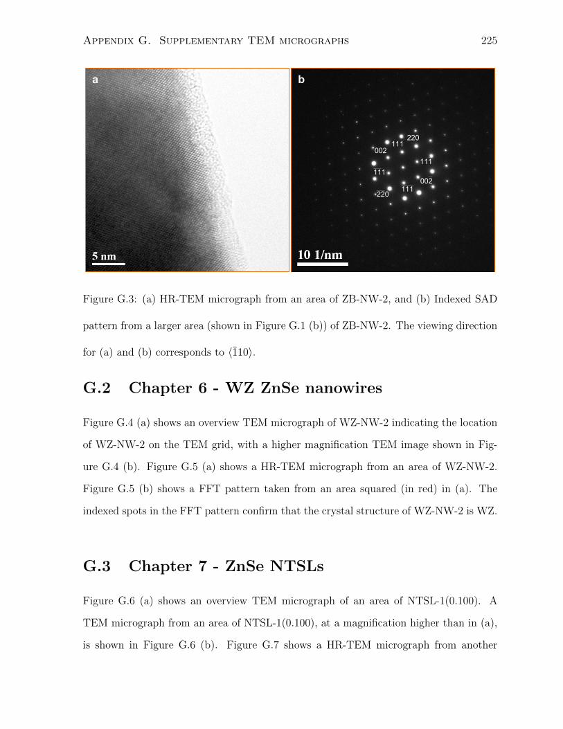
Appendix G. Supplementary TEM micrographs 225
a b
111
111
220
220
002
002111
111
Figure G.3: (a) HR-TEM micrograph from an area of ZB-NW-2, and (b) Indexed SAD
pattern from a larger area (shown in Figure G.1 (b)) of ZB-NW-2. The viewing direction
for (a) and (b) corresponds to 〈110〉.
G.2 Chapter 6 - WZ ZnSe nanowires
Figure G.4 (a) shows an overview TEM micrograph of WZ-NW-2 indicating the location
of WZ-NW-2 on the TEM grid, with a higher magnification TEM image shown in Fig-
ure G.4 (b). Figure G.5 (a) shows a HR-TEM micrograph from an area of WZ-NW-2.
Figure G.5 (b) shows a FFT pattern taken from an area squared (in red) in (a). The
indexed spots in the FFT pattern confirm that the crystal structure of WZ-NW-2 is WZ.
G.3 Chapter 7 - ZnSe NTSLs
Figure G.6 (a) shows an overview TEM micrograph of an area of NTSL-1(0.100). A
TEM micrograph from an area of NTSL-1(0.100), at a magnification higher than in (a),
is shown in Figure G.6 (b). Figure G.7 shows a HR-TEM micrograph from another
Appendix G. Supplementary TEM micrographs 226
a b
WZ-NW-2
Figure G.4: Structural characterization of WZ-NW-2: (a) Overview TEM micrograph,
and (b) TEM micrograph at a magnification higher than in (a).
a b
1101
11010002
0002
1100
1101
1101
1100
Figure G.5: (a) HR-TEM micrograph from an area of WZ-NW-2, (b) Indexed FFT
pattern acquired from an area (squared in red) in (a). The viewing direction for (a) and
(b) is 〈1100〉.

Appendix G. Supplementary TEM micrographs 227
area of NTSL-1(0.100), where atomically sharp interfaces at the twin-planes can be seen.
Figure G.8 (b) shows an indexed FFT pattern taken from an area highlighted in the
HR-TEM micrograph of NTSL-1(0.100), shown in Figure G.8 (a). The indexed spots
in the FFT pattern in (b) confirm that the individual domains in NTSL-1(0.100) are
〈111〉-ZB, with 〈111〉-direction coinciding with the growth direction of NTSL. Similar
TEM and HR-TEM micrographs, and FFT pattern for NTSL-2(0.077) are shown in
Figures G.9 (a,b), G.10 and G.11(a,b), respectively. Note that the diffraction spots in
the FFT pattern in Figure G.8 (b) are not as clear as those in Figure G.11 (b). This is
because a much smaller area was used in the former case for acquiring the FFT pattern.
a b
Figure G.6: Structural characterization of NTSL-1(0.100): (a) Overview TEM micro-
graph, and (b) HR-TEM micrograph from an area of NTSL-1(0.100). The viewing di-
rection for (a) and (b) is 〈110〉.
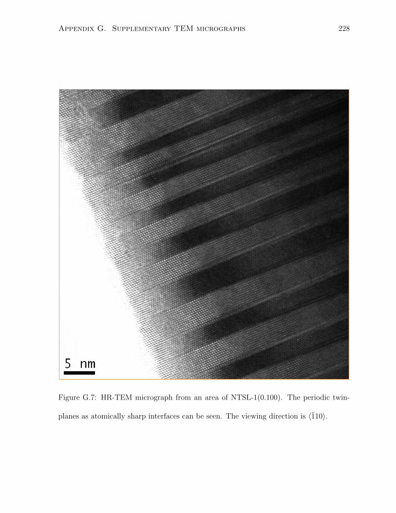
Appendix G. Supplementary TEM micrographs 228
Figure G.7: HR-TEM micrograph from an area of NTSL-1(0.100). The periodic twin-
planes as atomically sharp interfaces can be seen. The viewing direction is 〈110〉.
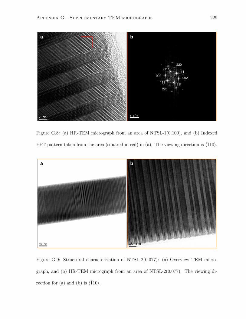
Appendix G. Supplementary TEM micrographs 229
a b
111
111
220
220
002002
111
111
Figure G.8: (a) HR-TEM micrograph from an area of NTSL-1(0.100), and (b) Indexed
FFT pattern taken from the area (squared in red) in (a). The viewing direction is 〈110〉.
a b
Figure G.9: Structural characterization of NTSL-2(0.077): (a) Overview TEM micro-
graph, and (b) HR-TEM micrograph from an area of NTSL-2(0.077). The viewing di-
rection for (a) and (b) is 〈110〉.
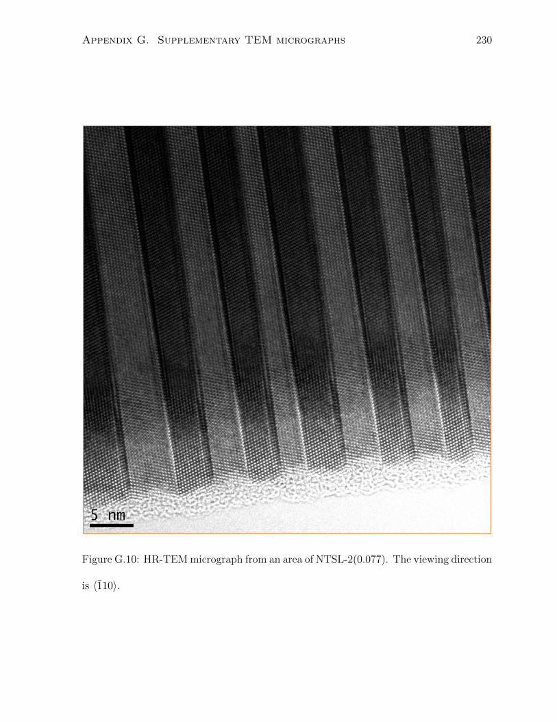
Appendix G. Supplementary TEM micrographs 230
Figure G.10: HR-TEM micrograph from an area of NTSL-2(0.077). The viewing direction
is 〈110〉.
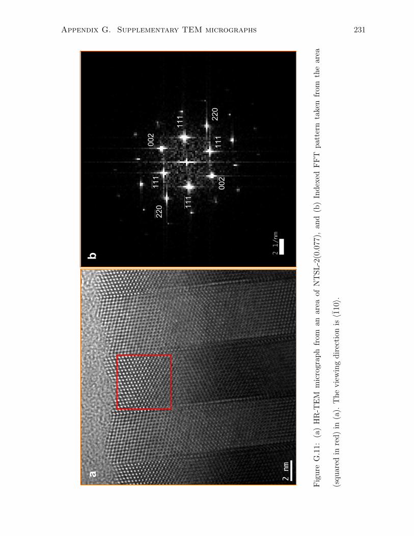
Appendix G. Supplementary TEM micrographs 231
ab
111
111
220
220
002
002
111
111
Fig
ure
G.1
1:(a
)H
R-T
EM
mic
rogr
aph
from
anar
eaof
NT
SL
-2(0
.077
),an
d(b
)In
dex
edF
FT
pat
tern
take
nfr
omth
ear
ea
(squar
edin
red)
in(a
).T
he
vie
win
gdir
ecti
onis〈1
10〉.

Appendix G. Supplementary TEM micrographs 232
Figure G.12 (a) shows an overview TEM micrograph of NTSL-3(0.059), and (b) shows
a HR-TEM micrograph from an area of NTSL-3(0.059). Figure G.13 shows a composite
image of the HR-TEM micrographs of NTSL-3(0.059). Figure G.14 (a) shows a HR-TEM
micrograph from another area of NTSL-3(0.059). The FFT pattern shown in Figure G.14
(b) was acquired from the area squared (in red) in Figure G.14 (a). The indexed spots in
the FFT pattern in (b) show that the individual domains in NTSL-3(0.059) are 〈111〉-ZB,
with 〈111〉-direction coinciding with the growth direction of NTSL. Figure G.15 (a) shows
a HR-TEM micrograph from another area of NTSL-3(0.059) and (b) shows an indexed
SAD pattern from an area of NTSL-3(0.059), shown in Figure G.12 (a). The diffraction
spots corresponding to two rotated ZB domains are shown with labels (with and without
a letter ‘T’). Double spots, characteristic of periodic twinning, seen in the SAD pattern
from an area of NTSL-3(0.059) highlight the excellent periodicity of twin-planes.
a b
Location of SAD
Figure G.12: Structural characterization of NTSL-3(0.059): (a) Overview TEM micro-
graph from an area of NTSL-3(0.059), and (b) a HR-TEM micrograph from an area of
NTSL-3(0.059). The viewing direction for (a) and (b) is 〈110〉.
Figures G.16 (a,b) show (a) an overview TEM micrograph and (b) a higher magnifica-
tion TEM micrograph from an area of NTSL-4(0.012). Figure G.17 (a) shows a HR-TEM
micrograph from an area of NTSL-4(0.012). The FFT pattern shown in Figure G.17 (b)
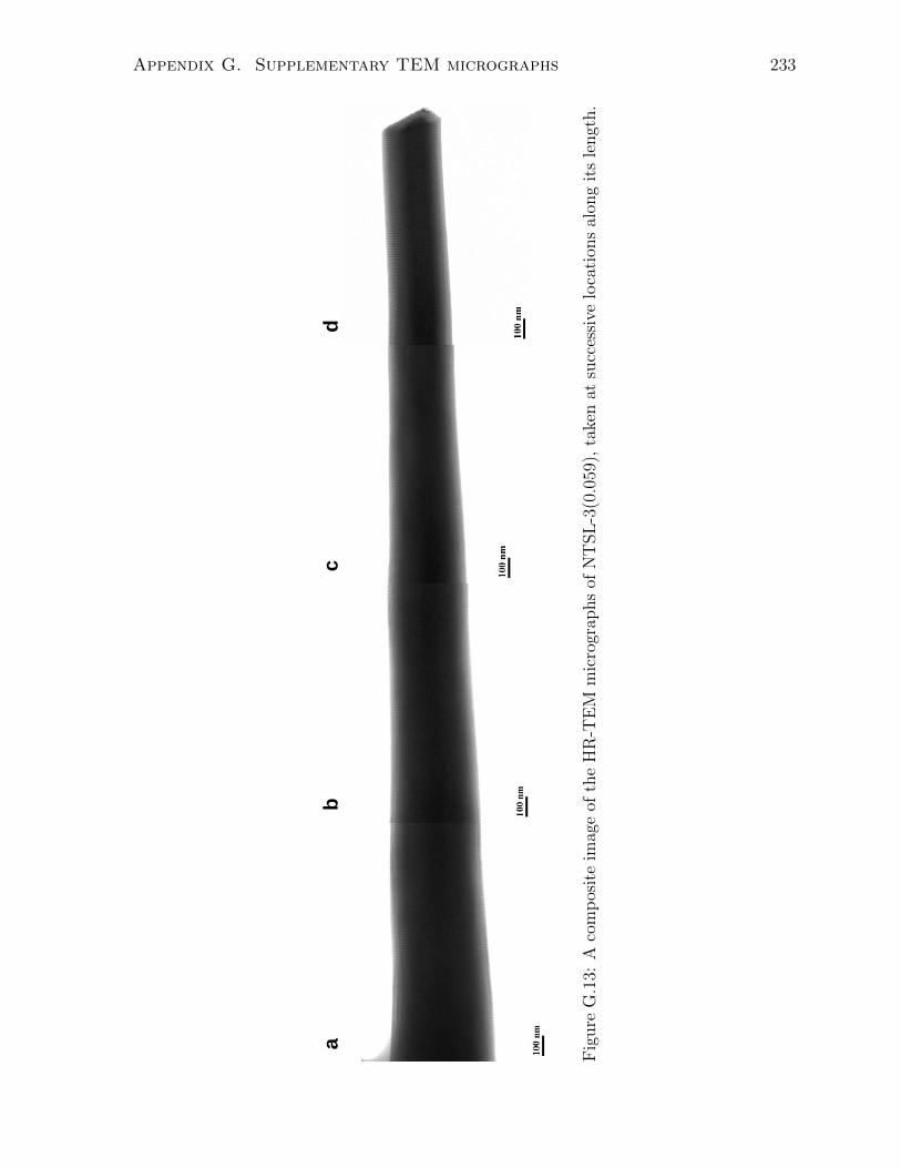
Appendix G. Supplementary TEM micrographs 233
a
b
c
d
Fig
ure
G.1
3:A
com
pos
ite
imag
eof
the
HR
-TE
Mm
icro
grap
hs
ofN
TSL
-3(0
.059
),ta
ken
atsu
cces
sive
loca
tion
sal
ong
its
lengt
h.
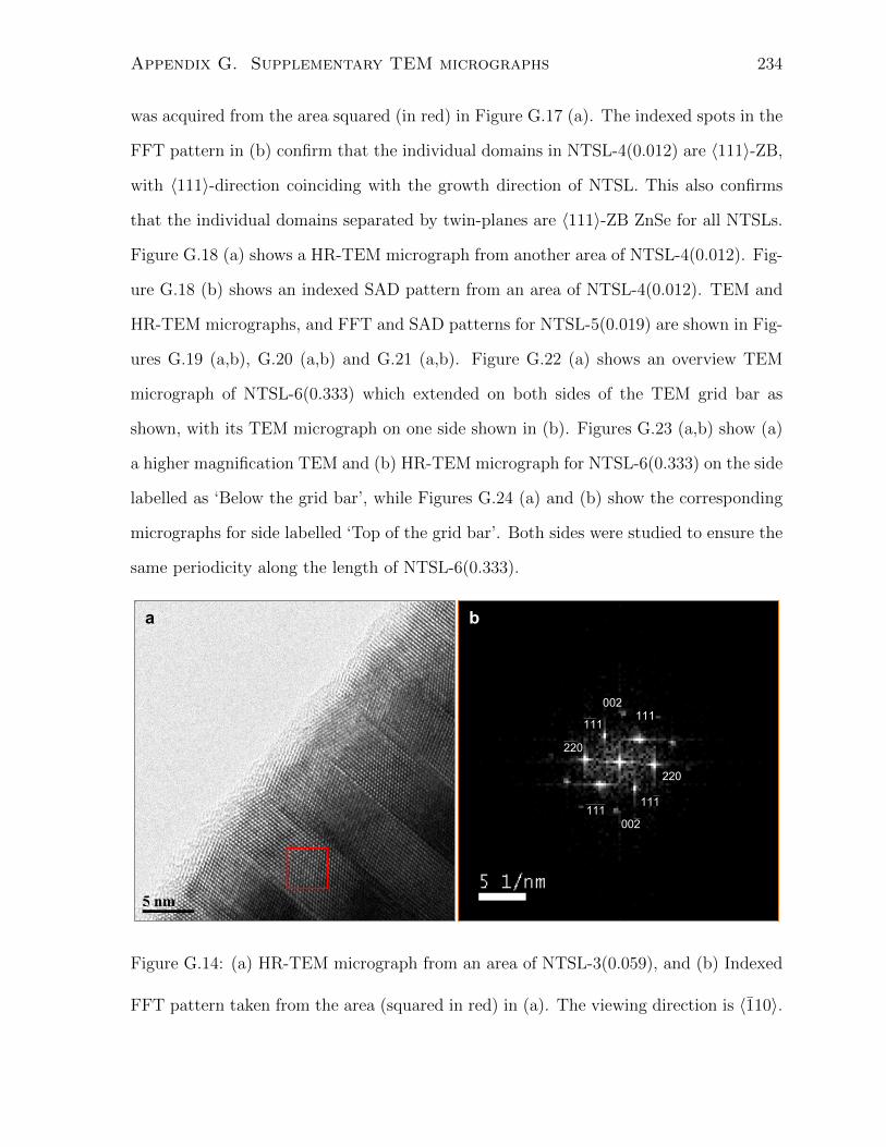
Appendix G. Supplementary TEM micrographs 234
was acquired from the area squared (in red) in Figure G.17 (a). The indexed spots in the
FFT pattern in (b) confirm that the individual domains in NTSL-4(0.012) are 〈111〉-ZB,
with 〈111〉-direction coinciding with the growth direction of NTSL. This also confirms
that the individual domains separated by twin-planes are 〈111〉-ZB ZnSe for all NTSLs.
Figure G.18 (a) shows a HR-TEM micrograph from another area of NTSL-4(0.012). Fig-
ure G.18 (b) shows an indexed SAD pattern from an area of NTSL-4(0.012). TEM and
HR-TEM micrographs, and FFT and SAD patterns for NTSL-5(0.019) are shown in Fig-
ures G.19 (a,b), G.20 (a,b) and G.21 (a,b). Figure G.22 (a) shows an overview TEM
micrograph of NTSL-6(0.333) which extended on both sides of the TEM grid bar as
shown, with its TEM micrograph on one side shown in (b). Figures G.23 (a,b) show (a)
a higher magnification TEM and (b) HR-TEM micrograph for NTSL-6(0.333) on the side
labelled as ‘Below the grid bar’, while Figures G.24 (a) and (b) show the corresponding
micrographs for side labelled ‘Top of the grid bar’. Both sides were studied to ensure the
same periodicity along the length of NTSL-6(0.333).
a b
111
111
220
220
002
002
111
111
Figure G.14: (a) HR-TEM micrograph from an area of NTSL-3(0.059), and (b) Indexed
FFT pattern taken from the area (squared in red) in (a). The viewing direction is 〈110〉.

Appendix G. Supplementary TEM micrographs 235
a b
11111
1
220 T
220
002 T
111 T
111 T
131 T
111
111
002
002 T
131
131 T
220
002
220 T
131
222
222
Figure G.15: (a) HR-TEM micrograph from an area of NTSL-3(0.059), and (b) Indexed
SAD pattern from a larger area (shown in Figure G.12 (a)) of NTSL-3(0.059). The
viewing direction for (a) and (b) is 〈110〉.
a b
Figure G.16: Structural characterization of NTSL-4(0.012): (a) Overview TEM micro-
graph from an area of NTSL-4(0.012), and (b) a TEM micrograph from an area of
NTSL-4(0.012), at a magnification higher than in (a) . The viewing direction for (b) is
〈110〉.
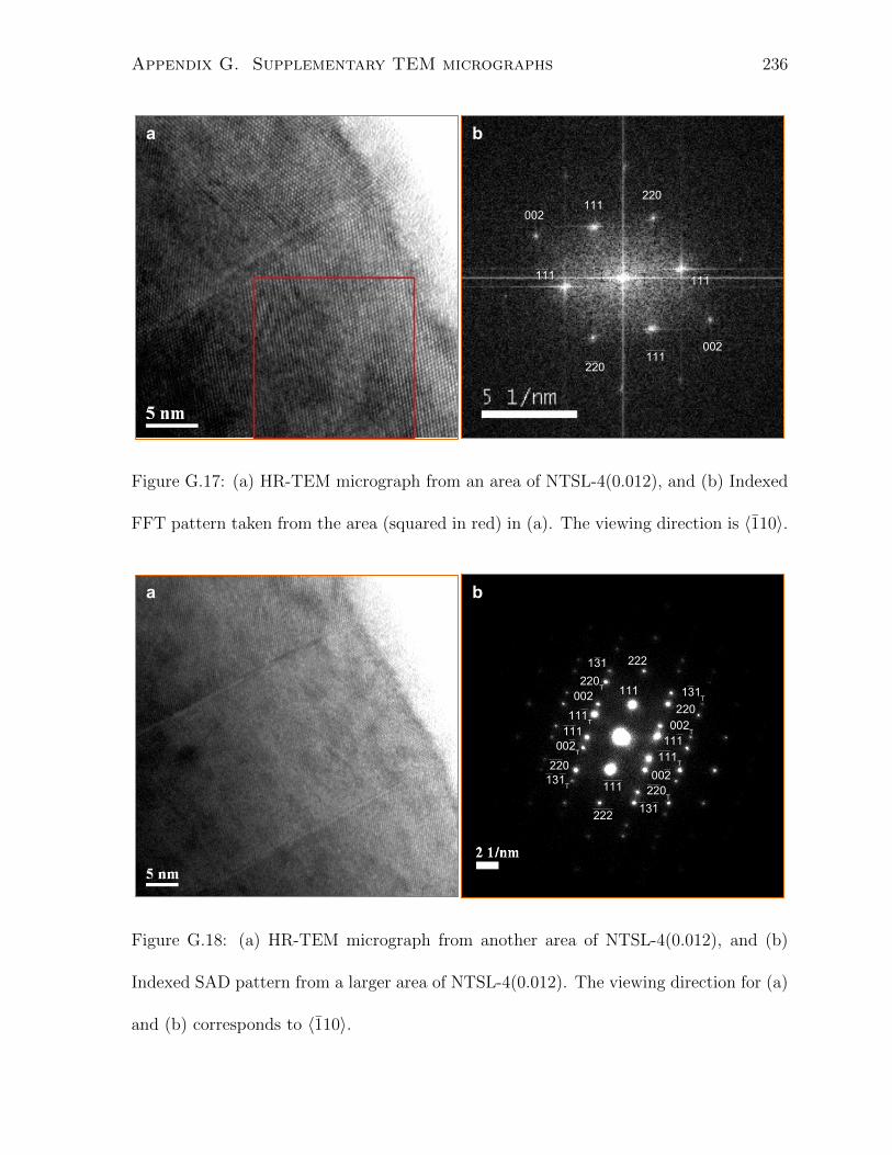
Appendix G. Supplementary TEM micrographs 236
a b
111
111
220
220
002
002
111 111
Figure G.17: (a) HR-TEM micrograph from an area of NTSL-4(0.012), and (b) Indexed
FFT pattern taken from the area (squared in red) in (a). The viewing direction is 〈110〉.
a b
111
111 220T
220T
002
111111
131
111T
111T
002T
002
131
131T
220
002T
220
131T
222
222
Figure G.18: (a) HR-TEM micrograph from another area of NTSL-4(0.012), and (b)
Indexed SAD pattern from a larger area of NTSL-4(0.012). The viewing direction for (a)
and (b) corresponds to 〈110〉.

Appendix G. Supplementary TEM micrographs 237
a b
Location of SAD
Figure G.19: Structural characterization of NTSL-5(0.019): (a) Overview TEM micro-
graph from an area of NTSL-5(0.019), and (b) a HR-TEM micrograph from an area of
NTSL-5(0.019). The viewing direction for (a) and (b) is 〈110〉.
a b
111
111
220
220
002
002111
111
Figure G.20: (a) HR-TEM micrograph from an area of NTSL-5(0.019), and (b) Indexed
FFT pattern taken from the area (squared in red) in (a). The viewing direction is 〈110〉.
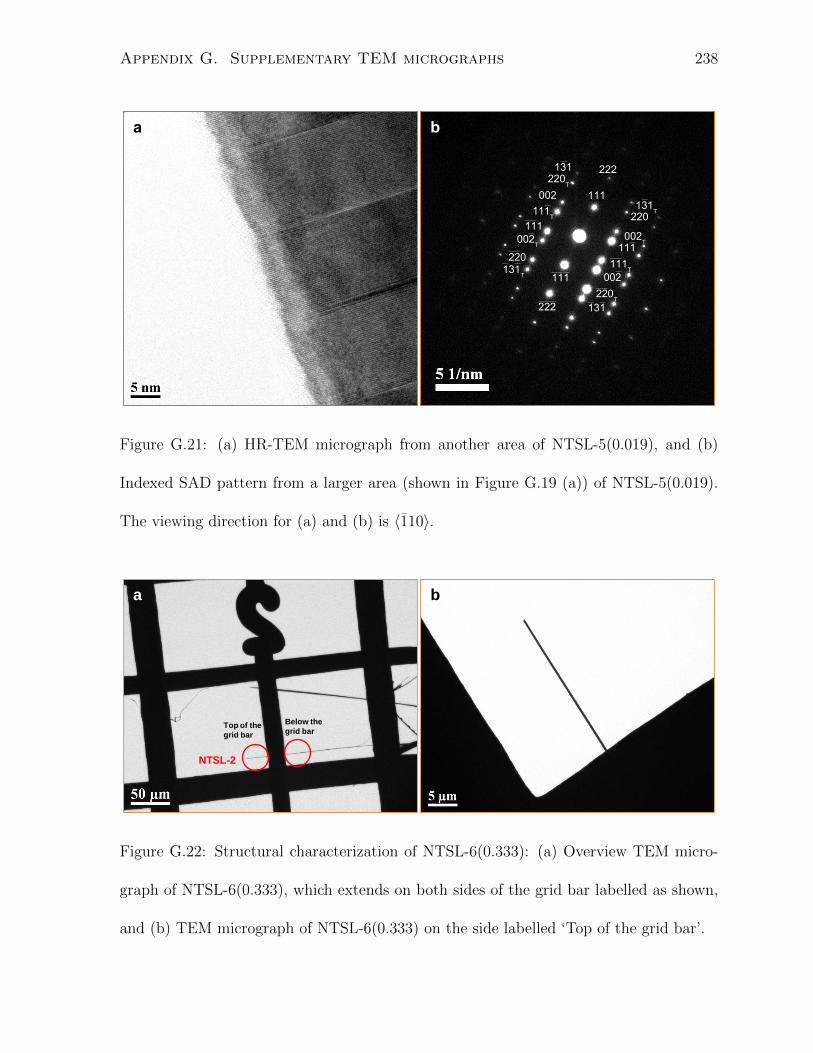
Appendix G. Supplementary TEM micrographs 238
a b
111
111
220T
220T
002
111
111
131
111T
111T
002T
002
131
131T
220
002T
220131
T
222
222
Figure G.21: (a) HR-TEM micrograph from another area of NTSL-5(0.019), and (b)
Indexed SAD pattern from a larger area (shown in Figure G.19 (a)) of NTSL-5(0.019).
The viewing direction for (a) and (b) is 〈110〉.
a b
Top of the
grid bar
Below the
grid bar
NTSL-2
Figure G.22: Structural characterization of NTSL-6(0.333): (a) Overview TEM micro-
graph of NTSL-6(0.333), which extends on both sides of the grid bar labelled as shown,
and (b) TEM micrograph of NTSL-6(0.333) on the side labelled ‘Top of the grid bar’.
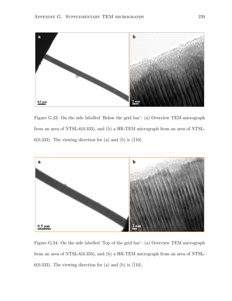
Appendix G. Supplementary TEM micrographs 239
a b
Figure G.23: On the side labelled ‘Below the grid bar’: (a) Overview TEM micrograph
from an area of NTSL-6(0.333), and (b) a HR-TEM micrograph from an area of NTSL-
6(0.333). The viewing direction for (a) and (b) is 〈110〉.
a b
Figure G.24: On the side labelled ‘Top of the grid bar’: (a) Overview TEM micrograph
from an area of NTSL-6(0.333), and (b) a HR-TEM micrograph from an area of NTSL-
6(0.333). The viewing direction for (a) and (b) is 〈110〉.

Bibliography
[1] K.F. Brennan. Introduction to Semiconductor Devices: For Computing and
Telecommunications Applications. Cambridge University Press, 2005.
[2] H. Morkoc, S. Strite, G.B. Gao, M.E. Lin, B. Sverdlov, and M. Burns. Large-band-
gap SiC, III-V nitride, and II-VI ZnSe-based semiconductor device technologies. J.
Appl. Phys., 76(3):1363–1398, 1994.
[3] G.F. Neumark. Defects in wide band gap II-VI crystals. Materials Science and
Engineering R: Reports, 21(1):iii–46, 1997.
[4] E Monroy, F Omnes, and F Calle. Wide-bandgap semiconductor ultraviolet pho-
todetectors. Semiconductor Science and Technology, 18(4):R33, 2003.
[5] D.R. Vij and N. Singh. Luminescence and Related Properties of II-VI Semiconduc-
tors. Nova Science Publishers Inc., 1998.
[6] H.E. Ruda. Widegap II-VI Compounds for Opto-electronic Applications. Chapman
and Hall, 1992.
[7] J. Gutowski, N. Presser, and G. Kudlek. Optical Properties of ZnSe Epilayers and
Films. physica status solidi (a), 120(1):11–59, 1990.
240
Bibliography 241
[8] Y.S. Park and B.K. Shin. Recent Advances in Injection Luminescence in II-VI
Compounds. In J. Pankove, editor, Electroluminescence, volume 17 of Topics in
Applied Physics, pages 133–170. Springer Berlin / Heidelberg, 1977.
[9] M. Aven and J.Z. Devine. Advances in Injection Luminescence of II-VI Compounds.
Journal of Luminescence, 7:195–212, 1973.
[10] W.M. Yim, J.P. Dismukes, E.J. Stofko, and R.J. Ulmer. Miscibility between ZnSe
and CdTe. physica status solidi (a), 13(1):K57–K61, 1972.
[11] R P Vijayalakshmi, R Venugopal, D R Reddy, and B K Reddy. Structural and
bandgap studies of ZnSxCdSe1−x thin films. Semiconductor Science and Technology,
9(5):1062–1068, 1994.
[12] R.W.G. Wyckoff. Crystal structures. Interscience Publishers, 1963.
[13] H. Hartmann. On the Growth of Hexagonal ZnSe Single Crystals. Kristall und
Technik, 5(4):527–534, 1970.
[14] B.J. Skromme. Luminescence as a Diagnostic of Wide-Gap II-VI Compound Semi-
conductor Materials. Annual Review of Materials Science, 25:601–646, 1995.
[15] H Luo and J K Furdyna. The II-VI semiconductor blue-green laser: challenges and
solution. Semiconductor Science and Technology, 10(8):1041–1048, 1995.
[16] L.A. Kolodziejski, R.L. Gunshor, and A.V. Nurmikko. Wide-Bandgap II-VI Het-
erostructures for Blue/Green Optical Sources: Key Materials Issues. Annual Review
of Materials Science, 25:711–753, 1995.
[17] Guihua Yu and Charles M. Lieber. Assembly and integration of semiconductor
nanowires for functional nanosystems. Pure and Applied Chemistry, 82(12):2295–
2314, 2010.

Bibliography 242
[18] Jiansheng Jie, Wenjun Zhang, Igor Bello, Chun-Sing Lee, and Shuit-Tong Lee.
One-dimensional II-VI nanostructures: Synthesis, properties and optoelectronic
applications. Nano Today, 5(4):313–336, 2010.
[19] Kimberly A. Dick. A review of nanowire growth promoted by alloys and non-
alloying elements with emphasis on Au-assisted III-V nanowires. Progress in Crystal
Growth and Characterization of Materials, 54(3-4):138–173, 2008.
[20] Xiaoxiao Li, Li Wang, and Guangqing Yan. Review: Recent research progress
on preparation of silver nanowires by soft solution method and their applications.
Crystal Research and Technology, 46(5):427–438, 2011.
[21] S. Picraux, Shadi Dayeh, Pradeep Manandhar, Daniel Perea, and Sukgeun Choi.
Silicon and Germanium Nanowires: Growth, Properties, and Integration. JOM
Journal of the Minerals, Metals and Materials Society, 62(4):35–43, 2010.
[22] Volker Schmidt, Joerg V. Wittemann, Stephan Senz, and Ulrich Gosele. Silicon
Nanowires: A Review on Aspects of their Growth and their Electrical Properties.
Advanced Materials, 21(25-26):2681–2702, 2009.
[23] J. Pan, H. Shen, and S. Mathur. One-dimensional SnO2 nanostructures: Synthesis
and Applications. Journal of Nanotechnology, 2012, 2012.
[24] Mildred S. Dresselhaus, Yu-Ming Lin, Oded Rabin, Marcie R. Black, Jing Kong,
and Gene Dresselhaus. Nanowires. In Bharat Bhushan, editor, Springer Handbook
of Nanotechnology, chapter 4, pages 119–167. Springer Berlin Heidelberg, 2010.
[25] H. Yu, J. Li, R.A. Loomis, L.-W. Wang, and W.E. Buhro. Two-versus three-
dimensional quantum confinement in indium phosphide wires and dots. Nature
Materials, 2(8):517–520, 2003.
Bibliography 243
[26] Peidong Yang, Ruoxue Yan, and Melissa Fardy. Semiconductor Nanowire: What’s
Next? Nano Letters, 10(5):1529–1536, 2010.
[27] Kwak J.-W. Park J.W. Choi, Y.-E. Nanotechnology for Early Cancer Detection.
Sensors, 10(1):428–455, 2010.
[28] Kannan and Balasubramanian. Challenges in the use of 1D nanostructures for
on-chip biosensing and diagnostics: A review. Biosensors and Bioelectronics,
26(4):1195–1204, 2010. Selected Papers from the World Congress on Biosen-
sors,Glasgow, Scotland, UK May 26-28, 2010.
[29] Xiaoqin Chi, Dengtong Huang, Zhenghuan Zhao, Zijian Zhou, Zhenyu Yin, and
Jinhao Gao. Nanoprobes for invitro diagnostics of cancer and infectious diseases.
Biomaterials, 33(1):189–206, 2012.
[30] Niranjan S. Ramgir, Yang Yang, and Margit Zacharias. Nanowire-Based Sensors.
Small, 6(16):1705–1722, 2010.
[31] R. Yan, D. Gargas, and P. Yang. Nanowire photonics. Nature Photonics, 3(10):569–
576, 2009.
[32] W. Lu and C.M. Lieber. Nanoelectronics from the bottom up. Nature Materials,
6(11):841–850, 2007.
[33] Wei Lu, Ping Xie, and C.M. Lieber. Nanowire Transistor Performance Limits and
Applications. Electron Devices, IEEE Transactions on, 55(11):2859–2876, 2008.
[34] C.M. Lieber. Semiconductor nanowires: A platform for nanoscience and nanotech-
nology. MRS Bulletin, 36(12):1052–1063, 2011.
[35] Bozhi Tian, Thomas J. Kempa, and Charles M. Lieber. Single nanowire photo-
voltaics. Chem. Soc. Rev., 38(1):16–24, 2009.
Bibliography 244
[36] Ke Sun, A. Kargar, Namsoek Park, K.N. Madsen, P.W. Naughton, T. Bright,
Yi Jing, and Deli Wang. Compound Semiconductor Nanowire Solar Cells. Selected
Topics in Quantum Electronics, IEEE Journal of, 17(4):1033–1049, 2011.
[37] L. VJ, J. Oh, A.P. Nayak, A.M. Katzenmeyer, K.H. Gilchrist, S. Grego, N.P.
Kobayashi, S.-Y. Wang, A.A. Talin, N.K. Dhar, and M.S. Islam. A Perspective on
Nanowire Photodetectors: Current Status, Future Challenges, and Opportunities.
Selected Topics in Quantum Electronics, IEEE Journal of, 17(4):1002–1032, 2011.
[38] D.O. Demchenko, P.D. Heinz, and B. Lee. Determining factors of thermoelectric
properties of semiconductor nanowires. Nanoscale Research Letters, 6(1):502, 2011.
[39] W Kim. Thermal transport in individual thermoelectric nanowires: a review. Ma-
terials Research Innovations, 15(6):375–385, 2011-11-01T00:00:00.
[40] Christopher J. Vineis, Ali Shakouri, Arun Majumdar, and Mercouri G. Kanatzidis.
Nanostructured Thermoelectrics: Big Efficiency Gains from Small Features. Ad-
vanced Materials, 22(36):3970–3980, 2010.
[41] Park J.-H.-Choi Y. Heo C.-J. Yang S.-M. Lee L.P. Yang P. Yan, R. Nanowire-based
single-cell endoscopy. Nature Nanotechnology, 7(3):191–196, 2011.
[42] Nam Hoon Kwon, Miles F. Beaux, Chad Ebert, Lidong Wang, Brian E. Lassiter,
Yong Ho Park, David N. McIlroy, Carolyn J. Hovde, and Gregory A. Bohach.
Nanowire-Based Delivery of Escherichia coli O157 Shiga Toxin 1 A Subunit into
Human and Bovine Cells. Nano Letters, 7(9):2718–2723, 2007.
[43] J.C. Johnson, H.-J. Choi, K.P. Knutsen, R.D. Schaller, P. Yang, and R.J. Saykally.
Single gallium nitride nanowire lasers. Nature Materials, 1(2):106–110, 2002.
Bibliography 245
[44] Michael H. Huang, Samuel Mao, Henning Feick, Haoquan Yan, Yiying Wu, Hannes
Kind, Eicke Weber, Richard Russo, and Peidong Yang. Room-Temperature Ultra-
violet Nanowire Nanolasers. Science, 292(5523):1897–1899, 2001.
[45] Wang G.-Zhou-W. Lin Y. Chernyak-L. Zhao J.-Kong J. Li L. Ren J. Liu J. Chu, S.
Electrically pumped waveguide lasing from ZnO nanowires. Nature Nanotechnology,
6(8):506–510, 2011.
[46] Mariano A Zimmler, Federico Capasso, Sven Muller, and Carsten Ronning. Opti-
cally pumped nanowire lasers: invited review. Semiconductor Science and Tech-
nology, 25(2):024001, 2010.
[47] C.Z. Ning. Semiconductor nanolasers. physica status solidi (b), 247(4):774–788,
2010.
[48] Daniel Vanmaekelbergh and Lambert K. van Vugt. ZnO nanowire lasers. Nanoscale,
3(7):2783–2800, 2011.
[49] P. Yang, H. Yan, S. Mao, R. Russo, J. Johnson, R. Saykally, N. Morris, J. Pham,
R. He, and H.-J. Choi. Controlled Growth of ZnO Nanowires and Their Optical
Properties. Advanced Functional Materials, 12(5):323–331, 2002.
[50] Zhong Lin Wang. Zinc oxide nanostructures: growth, properties and applications.
Journal of Physics: Condensed Matter, 16(25):R829–R858, 2004.
[51] Xuchuan Jiang, Yi Xie, Jun Lu, Liying Zhu, Wei He, and Yitai Qian. Simultaneous
In Situ Formation of ZnS Nanowires in a Liquid Crystal Template by γ-Irradiation.
Chemistry of Materials, 13(4):1213–1218, 2001.
[52] Dongsheng Xu, Xuesong Shi, Guolin Guo, Linlin Gui, and Youqi Tang. Electro-
chemical Preparation of CdSe Nanowire Arrays. The Journal of Physical Chemistry
B, 104(21):5061–5063, 2000.
Bibliography 246
[53] L.V. Titova, Thang Ba Hoang, H.E. Jackson, L.M. Smith, J.M. Yarrison-Rice, J.L.
Lensch, and L.J. Lauhon. Low-temperature photoluminescence imaging and time-
resolved spectroscopy of single CdS nanowires. Appl. Phys. Lett., 89(5):053119,
2006.
[54] Tianyou Zhai, Xiaosheng Fang, Liang Li, Yoshio Bando, and Dmitri Golberg.
One-dimensional CdS nanostructures: synthesis, properties, and applications.
Nanoscale, 2(2):168–187, 2010.
[55] B. Xiang, H.Z. Zhang, G.H. Li, F.H. Yang, F.H. Su, R.M. Wang, J. Xu, G.W. Lu,
X.C. Sun, Q. Zhao, and D.P. Yu. Green-light-emitting ZnSe nanowires fabricated
via vapor phase growth. Appl. Phys. Lett., 82(19):3330–3332, 2003.
[56] Ying-Chun Zhu and Yoshio Bando. Preparation and photoluminescence of single-
crystal zinc selenide nanowires. Chemical Physics Letters, 377(3-4):367–370, 2003.
[57] X.T. Zhang, Z. Liu, Y.P. Leung, Quan Li, and S.K. Hark. Growth and lumines-
cence of zinc-blende-structured ZnSe nanowires by metal-organic chemical vapor
deposition. Appl. Phys. Lett., 83(26):5533–5535, 2003.
[58] Ruitao Lv, Chuanbao Cao, Huazhang Zhai, Dazhi Wang, Siyuan Liu, and Hesun
Zhu. Growth and characterization of single-crystal ZnSe nanorods via surfactant
soft-template method. Solid State Communications, 130(3-4):241–245, 2004.
[59] X.T. Zhang, Z. Liu, K.M. Ip, Y.P. Leung, Quan Li, and S.K. Hark. Luminescence
of ZnSe nanowires grown by metalorganic vapor phase deposition under different
pressures. J. Appl. Phys., 95(10):5752–5755, 2004.
[60] C. Ye, X. Fang, Y. Wang, P. Yan, J. Zhao, and L. Zhang. Structural characteriza-
tion of long ZnSe nanowires. Applied Physics A: Materials Science & Processing,
79(1):113–115, 2004.
Bibliography 247
[61] Yang Jiang, Xiang-Min Meng, Wing-Ching Yiu, Ji Liu, Jun-Xian Ding, Chun-Sing
Lee, and Shuit-Tong Lee. Zinc Selenide Nanoribbons and Nanowires. The Journal
of Physical Chemistry B, 108(9):2784–2787, 2004.
[62] Minghai Chen and Lian Gao. Synthesis and characterization of wurtzite ZnSe one-
dimensional nanocrystals through molecular precursor decomposition by solvother-
mal method. Materials Chemistry and Physics, 91(2-3):437–441, 2005.
[63] S. Xiong, J. Shen, Q. Xie, Y. Gao, Q. Tang, and Y.T. Qian. A Precursor-Based
Route to ZnSe Nanowire Bundles. Advanced Functional Materials, 15(11):1787–
1792, 2005.
[64] Y.P. Leung, Z. Liu, and S.K. Hark. Changes in morphology and growth rate of
quasi-one-dimensional ZnSe nanowires on GaAs (100) substrates by metalorganic
chemical vapor deposition. Journal of Crystal Growth, 279(3-4):248–257, 2005.
[65] K M Ip, Z Liu, C M Ng, and S K Hark. Effects of passivation and ambient gases on
the photoluminescence of ZnSe nanowires. Nanotechnology, 16(8):1144–1147, 2005.
[66] X. Zhang, Z. Liu, Q. Li, Y. Leung, K. Ip, and S. Hark. Routes to Grow Well-Aligned
Arrays of ZnSe Nanowires and Nanorods. Advanced Materials, 17(11):1405–1410,
2005.
[67] A Colli, S Hofmann, A C Ferrari, F Martelli, S Rubini, C Ducati, A Franciosi, and
J Robertson. Selective growth of ZnSe and ZnCdSe nanowires by molecular beam
epitaxy. Nanotechnology, 16(5):S139–S142, 2005.
[68] Junqing Hu, Yoshio Bando, and Dmitri Golberg. Sn-Catalyzed Thermal Evapora-
tion Synthesis of Tetrapod-Branched ZnSe Nanorod Architectures. Small, 1(1):95–
99, 2005.

Bibliography 248
[69] A.B. Panda, S. Acharya, and S. Efrima. Ultranarrow ZnSe Nanorods and
Nanowires: Structure, Spectroscopy, and One-Dimensional Properties. Advanced
Materials, 17(20):2471–2474, 2005.
[70] Y.P. Leung, Wallace C.H. Choy, I. Markov, G.K.H. Pang, H.C. Ong, and T.I. Yuk.
Synthesis of wurtzite ZnSe nanorings by thermal evaporation. Appl. Phys. Lett.,
88(18):183110, 2006.
[71] J. Salfi, U. Philipose, C.F. de Sousa, S. Aouba, and H.E. Ruda. Electrical proper-
ties of Ohmic contacts to ZnSe nanowires and their application to nanowire-based
photodetection. Appl. Phys. Lett., 89(26):261112, 2006.
[72] U. Philipose, T. Xu, S. Yang, Ping Sun, Harry E. Ruda, Y.Q. Wang, and K.L.
Kavanagh. Enhancement of band edge luminescence in ZnSe nanowires. J. Appl.
Phys., 100(8):084316, 2006.
[73] Hui Song, Dazhi Wang, Xichen Ma, Yafeng Cao, and Shufen Zhang. Soft ZnSe
nanobelts: Characterization and feasibility for assembling tubular ZnSe nanostruc-
tures. Solid State Communications, 139(8):430–433, 2006.
[74] Xia Dong-Yan, Dai Lun, Xu Wan-Jin, You Li-Ping, Zhang Bo-Rui, Ran Guang-
Zhao, and Qin Guo-Gang. Synthesis and PL Properties of ZnSe Nanowires with
Zincblende and Wurtzite Structures. Chinese Physics Letters, 23(5):1317, 2006.
[75] Hongzhi Fu, Huanyong Li, Wanqi Jie, and Lan Yang. The growth and characteri-
zation of ZnSe nanoneedles by a simple chemical vapor deposition method. Journal
of Crystal Growth, 289(2):440–444, 2006.
[76] Lei Jin, Wallace C.H. Choy, Yee P. Leung, Tong I. Yuk, Hock C. Ong, and Jian
bo Wang. Synthesis and analysis of abnormal wurtzite ZnSe nanowheels. J. Appl.
Phys., 102(4):044302, 2007.
Bibliography 249
[77] Y.Q. Wang, U. Philipose, T. Xu, H.E. Ruda, and K.L. Kavanagh. Twinning mod-
ulation in ZnSe nanowires. Semiconductor Science and Technology, 22(3):175–178,
2007.
[78] U. Philipose, S. Yang, T. Xu, and Harry E. Ruda. Origin of the red lumines-
cence band in photoluminescence spectra of ZnSe nanowires. Appl. Phys. Lett.,
90(6):063103, 2007.
[79] S. Acharya, A.B. Panda, S. Efrima, and Y. Golan. Polarization Properties
and Switchable Assembly of Ultranarrow ZnSe Nanorods. Advanced Materials,
19(8):1105–1108, 2007.
[80] Yuan-yuan Zhang, Jia-fu Chen, Xu-sheng Zheng, and Xue-hui Dong. Preparation
of Manganese-doped ZnSe Precursor Nanoribbon Bundles and Investigation of its
Magneto-optical Properties. Chinese Journal of Chemical Physics, 20(5):607, 2007.
[81] U. Philipose, Ping Sun, Tao Xu, Harry E. Ruda, L. Yang, and K.L. Kavanagh.
Structure and photoluminescence of ZnSe nanostructures fabricated by vapor phase
growth. J. Appl. Phys., 101(1):014326, 2007.
[82] Feifei Wang, Zhihua Zhang, Ruibin Liu, Xiao Wang, Xing Zhu, Anlian Pan, and
Bingsuo Zou. Structure and stimulated emission of ZnSe nanoribbons grown by
thermal evaporation. Nanotechnology, 18(30):305705, 2007.
[83] Asit Baran Panda, Somobrata Acharya, Shlomo Efrima, and Yuval Golan. Syn-
thesis, Assembly, and Optical Properties of Shape- and Phase-Controlled ZnSe
Nanostructures. Langmuir, 23(2):765–770, 2007.
[84] Z.D. Hu, X.F. Duan, M. Gao, Q. Chen, and L.-M. Peng. ZnSe Nanobelts and
Nanowires Synthesized by a Closed Space Vapor Transport Technique. The Journal
of Physical Chemistry C, 111(7):2987–2991, 2007.

Bibliography 250
[85] U Philipose, Ankur Saxena, Harry E Ruda, P J Simpson, Y Q Wang, and K L
Kavanagh. Defect studies of ZnSe nanowires. Nanotechnology, 19(21):215715, 2008.
[86] Sivakumar Ramanathan, Sridhar Patibandla, Supriyo Bandyopadhyay, John An-
derson, and Jarrod D Edwards. Fluorescence spectroscopy of electrochemically
self-assembled ZnSe and Mn:ZnSe nanowires. Nanotechnology, 19(19):195601, 2008.
[87] Junli Wang and Qing Yang. One-Dimensional Angle-Shaped ZnSe Nanostructures:
Synthesis and Formation Mechanism. Crystal Growth & Design, 8(2):660–664,
2008.
[88] Xia Fan, Xiang Min Meng, Xiao Hong Zhang, Ming Liang Zhang, Jian Sheng Jie,
Wen Jun Zhang, Chun Sing Lee, and Shuit Tong Lee. Formation and Photoelectric
Properties of Periodically Twinned ZnSe/SiO2 Nanocables. The Journal of Physical
Chemistry C, 113(3):834–838, 2009.
[89] Bo Hou, Yanjuan Li, Yongjun Liu, Bo Yuan, Mingfen Jia, and Fengzhi Jiang. A
simple way of shape-controlled synthesis of ZnSe nanocrystals: nanodots, nanoflow-
ers, and nanotubes. CrystEngComm, 11(9):1789–1792, 2009.
[90] Liang Shi, Yeming Xu, and Quan Li. Controlled Fabrication of ZnSe Arrays of
Well-Aligned Nanorods, Nanowires, and Nanobelts with a Facile Template-Free
Route. The Journal of Physical Chemistry C, 113(5):1795–1799, 2009.
[91] C. Lee, S. Park, and J. Jun. Enhanced Photoluminescence of ZnSe Nanowires with
Branches. Journal of the Korean Physical Society, 55(2):554–557, 2009.
[92] Patrick T.K. Chin, Jan W. Stouwdam, and Rene A.J. Janssen. Highly Luminescent
Ultranarrow Mn Doped ZnSe Nanowires. Nano Letters, 9(2):745–750, 2009.
Bibliography 251
[93] Chung-Liang Cheng and Yang-Fang Chen. Low temperature synthesis of ZnSe
nanowires by self-catalytic liquid-solid growth. Materials Chemistry and Physics,
115(1):158–160, 2009.
[94] Haitao Wang, Tian Tian, Shancheng Yan, Ningping Huang, and Zhongdang Xiao.
Large-scale synthesis of ZnSe nanoribbons on zinc substrate. Journal of Crystal
Growth, 311(14):3787–3791, 2009.
[95] Jun Liu and Dongfeng Xue. Solution-based route to semiconductor film: Well-
aligned ZnSe nanobelt arrays. Thin Solid Films, 517(17):4814–4817, 2009.
[96] Lihui Zhang and Heqing Yang. The Ag+ induced solution-liquid-solid growth,
photoluminescence and photocatalytic activity of twinned ZnSe nanowires. Applied
Physics A: Materials Science & Processing, 98(4):801–810, 2010.
[97] Yinxiao Du and Qing-Xin Yuan. Facile synthesis and photoluminescence of ZnSe
nanowires. Journal of Alloys and Compounds, 492(1-2):548–551, 2010.
[98] T.K. Das, R. Bhattacharya, A. Manna, and S. Saha. Role of reducing agent in
the formation of ZnSe nanorods by chemical reduction method. European Physical
Journal Applied Physics, 51:30605, 2010.
[99] Dongmei Han, Chunfeng Song, and Xiaoyu Li. Synthesis and Fluorescence Property
of Mn-Doped ZnSe Nanowires. Journal of Nanomaterials, 2010:290763, 2010.
[100] M. Huang. Synthesis and photoluminescence properties of washboard belt-like ZnSe
nanostructures. Optoelectronics and Advanced Materials-Rapid Communications,
4(12):2076–2079, 2010.
[101] Tingting Yao, Qing Zhao, Zhengping Qiao, Feng Peng, Hongjuan Wang, Hao
Yu, Cheng Chi, and Jian Yang. Chemical Synthesis, Structural Characteriza-
Bibliography 252
tion, Optical Properties, and Photocatalytic Activity of Ultrathin ZnSe Nanorods.
Chemistry–A European Journal, 17(31):8663–8670, 2011.
[102] H.W. Zhu, P.G. Li, M. Lei, L.H. Li, S.L. Wang, and W.H. Tang. Sublimation sand-
wich route to ultralong zinc-blende ZnSe nanowires and the cathodoluminescence
properties of individual nanowires. Journal of Alloys and Compounds, 509(7):3306–
3309, 2011.
[103] X.T. Zhang, K.M. Ip, Z. Liu, Y.P. Leung, Quan Li, and S.K. Hark. Structure and
photoluminescence of ZnSe nanoribbons grown by metal organic chemical vapor
deposition. Appl. Phys. Lett., 84(14):2641–2643, 2004.
[104] Q. Li, X. Gong, C. Wang, J. Wang, K. Ip, and S. Hark. Size-Dependent Periodically
Twinned ZnSe Nanowires. Advanced Materials, 16(16):1436–1440, 2004.
[105] Yutaka Ohno, Takeo Shirahama, Seiji Takeda, Atsushi Ishizumi, and Yoshihiko
Kanemitsu. Fe-catalytic growth of ZnSe nanowires on a ZnSe(001) surface at low
temperatures by molecular-beam epitaxy. Appl. Phys. Lett., 87(4):043105, 2005.
[106] X.T. Zhang, K.M. Ip, Quan Li, and S.K. Hark. Photoluminescence of Ag-doped
ZnSe nanowires synthesized by metalorganic chemical vapor deposition. Appl. Phys.
Lett., 86(20):203114, 2005.
[107] C X Shan, Z Liu, X T Zhang, C C Wong, and S K Hark. Wurtzite ZnSe nanowires:
growth, photoluminescence, and single-wire Raman properties. Nanotechnology,
17(22):5561–5564, 2006.
[108] Z Liu and S K Hark. Localized cathodoluminescence of individual ZnSe nanorods.
Nanotechnology, 17(5):1355–1358, 2006.
Bibliography 253
[109] S.Y. Liu, Wallace C.H. Choy, L. Jin, Y.P. Leung, G.P. Zheng, Jianbo Wang, and
A.K. Soh. Triple-Crystal Zinc Selenide Nanobelts. The Journal of Physical Chem-
istry C, 111(26):9055–9059, 2007.
[110] Adrien Tribu, Gregory Sallen, Thomas Aichele, Regis Andre, Jean-Philippe Poizat,
Catherine Bougerol, Serge Tatarenko, and Kuntheak Kheng. A High-Temperature
Single-Photon Source from Nanowire Quantum Dots. Nano Letters, 8(12):4326–
4329, 2008.
[111] Thomas Aichele, Adrien Tribu, Catherine Bougerol, Kuntheak Kheng, Regis Andre,
and Serge Tatarenko. Defect-free ZnSe nanowire and nanoneedle nanostructures.
Appl. Phys. Lett., 93(14):143106, 2008.
[112] Ankur Saxena, Suxia Yang, U. Philipose, and Harry E. Ruda. Excitonic and pair-
related photoluminescence in ZnSe nanowires. J. Appl. Phys., 103(5):053109, 2008.
[113] Y.P. Leung, Wallace C.H. Choy, and T.I. Yuk. Linearly resistive humidity sensor
based on quasi one-dimensional ZnSe nanostructures. Chemical Physics Letters,
457(1-3):198–201, 2008.
[114] B.J. Cooley, T.E. Clark, B.Z. Liu, C.M. Eichfeld, E.C. Dickey, S.E. Mohney,
S.A. Crooker, and N. Samarth. Growth of Magneto-optically Active (Zn,Mn)Se
Nanowires. Nano Letters, 9(9):3142–3146, 2009.
[115] Thomas Aichele, Adrien Tribu, Gregory Sallen, Juanita Bocquel, Edith Bellet-
Amalric, Catherine Bougerol, Jean-Philippe Poizat, Kuntheak Kheng, Regis Andre,
Serge Tatarenko, and Henri Mariette. CdSe quantum dots in ZnSe nanowires as effi-
cient source for single photons up to 220 K. Journal of Crystal Growth, 311(7):2123–
2127, 2009. International Conference on Molecular Beam Epitaxy (MBE-XV)-The
15th International Conference on Molecular Beam Epitaxy (MBE-XV).

Bibliography 254
[116] Thomas Aichele, Adrien Tribu, Catherine Bougerol, Kuntheak Kheng, Fabrice Do-
natini, Le Si Dang, Regis Andre, and Serge Tatarenko. Growth and properties of
defect-free ZnSe nanowires and nanoneedles. physica status solidi (b), 246(4):812–
815, 2009.
[117] C.H. Hsiao, S.J. Chang, S.B. Wang, S.C. Hung, S.P. Chang, T.C. Li, W.J. Lin,
and B.R. Huang. MBE growth of ZnSe nanowires on oxidized silicon substrate.
Superlattices and Microstructures, 46(4):572–577, 2009.
[118] C.H. Hsiao, S.J. Chang, S.B. Wang, S.P. Chang, T.C. Li, W.J. Lin, C.H. Ko,
T.M. Kuan, and B.R. Huang. ZnSe Nanowire Photodetector Prepared on Oxidized
Silicon Substrate by Molecular-Beam Epitaxy. Journal of The Electrochemical
Society, 156(4):J73–J76, 2009.
[119] Shanying Li, Yang Jiang, Binbin Wang, Di Wu, Junwei Li, Yugang Zhang, Ben
Yang, Xianan Ding, Hongyang Zhou, and Honghai Zhong. Synthesis of p-type
ZnSe nanowires by atmosphere compensating technique. Micro & Nano Letters,
6(6):459–462, 2011.
[120] Yao Liang, Yin Tao, and S.K. Hark. Fabrication and optical properties of ver-
tically aligned ZnSe nanowire arrays catalyzed by Ga and Ag. CrystEngComm,
13(19):5751–5754, 2011.
[121] Xiaosheng Fang, Shenglin Xiong, Tianyou Zhai, Yoshio Bando, Meiyong Liao,
Ujjal K. Gautam, Yasuo Koide, Xiaogang Zhang, Yitai Qian, and Dmitri Gol-
berg. High-Performance Blue/Ultraviolet-Light-Sensitive ZnSe-Nanobelt Photode-
tectors. Advanced Materials, 21(48):5016–5021, 2009.
[122] P. Caroff, J. Bolinsson, and J. Johansson. Crystal Phases in III-V Nanowires: From
Random Toward Engineered Polytypism. Selected Topics in Quantum Electronics,
IEEE Journal of, 17(4):829–846, 2011.
Bibliography 255
[123] Xiaosheng Fang, Yoshio Bando, Ujjal K. Gautam, Tianyou Zhai, Silvija Gradecak,
and Dmitri Golberg. Heterostructures and superlattices in one-dimensional
nanoscale semiconductors. J. Mater. Chem., 19(32):5683–5689, 2009.
[124] P. Caroff, K.A. Dick, J. Johansson, M.E. Messing, K. Deppert, and L. Samuel-
son. Controlled polytypic and twin-plane superlattices in III-V nanowires. Nature
Nanotech., 4:50–55, 2009.
[125] Jessica Bolinsson, Philippe Caroff, Bernhard Mandl, and Kimberly A Dick.
Wurtzite–zincblende superlattices in InAs nanowires using a supply interruption
method. Nanotechnology, 22(26):265606, 2011.
[126] N. Akopian, G. Patriarche, L. Liu, J.-C. Harmand, and V. Zwiller. Crystal Phase
Quantum Dots. Nano Letters, 10(4):1198–1201, 2010.
[127] Kuranananda Pemasiri, Mohammad Montazeri, Richard Gass, Leigh M. Smith,
Howard E. Jackson, Jan Yarrison-Rice, Suriati Paiman, Qiang Gao, H. Hoe Tan,
Chennupati Jagadish, Xin Zhang, and Jin Zou. Carrier Dynamics and Quan-
tum Confinement in type II ZB-WZ InP Nanowire Homostructures. Nano Letters,
9(2):648–654, 2009.
[128] A. Pan, P.L. Nichols, and C.Z. Ning. Semiconductor Alloy Nanowires and
Nanobelts With Tunable Optical Properties. Selected Topics in Quantum Elec-
tronics, IEEE Journal of, 17(4):808–818, 2011.
[129] Xiujuan Zhuang, C.Z. Ning, and Anlian Pan. Composition and Bandgap-Graded
Semiconductor Alloy Nanowires. Advanced Materials, 24(1):13–33, 2012.
[130] Lorenzo Pavesi and Mario Guzzi. Photoluminescence of AlxGa1−xAs alloys. J.
Appl. Phys., 75(10):4779–4842, 1994.

Bibliography 256
[131] Yufeng Hao, Guowen Meng, Zhong Lin Wang, Changhui Ye, and Lide Zhang.
Periodically Twinned Nanowires and Polytypic Nanobelts of ZnS: The Role of
Mass Diffusion in Vapor-Liquid-Solid Growth. Nano Letters, 6(8):1650–1655, 2006.
[132] R.E. Algra, M.A. Verheijen, M.T. Borgstrom, L.-F. Feiner, G. Immink, W.J.P.
Van Enckevort, E. Vlieg, and E.P.A.M. Bakkers. Twinning superlattices in indium
phosphide nanowires. Nature, 456(7220):369–372, 2008.
[133] Jiming Bao, David C. Bell, Federico Capasso, Jakob B. Wagner, Thomas
Martensson, Johanna Tragardh, and Lars Samuelson. Optical Properties of Ro-
tationally Twinned InP Nanowire Heterostructures. Nano Letters, 8(3):836–841,
2008.
[134] Chin-Yu Yeh, Z.W. Lu, S. Froyen, and Alex Zunger. Zinc-blende–wurtzite poly-
typism in semiconductors. Phys. Rev. B, 46(16):10086–10097, 1992.
[135] B.Y. Geng, X.W. Liu, Q.B. Du, X.W. Wei, and L.D. Zhang. Structure and optical
properties of periodically twinned ZnS nanowires. Appl. Phys. Lett., 88(16):163104,
2006.
[136] Frederic Sansoz. Surface Faceting Dependence of Thermal Transport in Silicon
Nanowires. Nano Letters, 11(12):5378–5382, 2011.
[137] Z. Ikonic, G.P. Srivastava, and J.C. Inkson. Twinning superlattices. Solid State
Commun., 86(12):799–802, 1993.
[138] Z. Ikonic, G.P. Srivastava, and J.C. Inkson. Optical properties of twinning su-
perlattices in diamond-type and zinc-blende-type semiconductors. Phys. Rev. B,
52(19):14078–14085, 1995.
[139] Sajal Dhara, Hari S. Solanki, Arvind Pawan R., Vibhor Singh, Shamashis Sengupta,
B.A. Chalke, Abhishek Dhar, Mahesh Gokhale, Arnab Bhattacharya, and Man-

Bibliography 257
dar M. Deshmukh. Tunable thermal conductivity in defect engineered nanowires
at low temperatures. Phys. Rev. B, 84(12):121307(R), 2011.
[140] P.L. Edwards and R.J. Happel Jr. Beryllium Oxide Whiskers and Platelets. J.
Appl. Phys., 33(3):943–948, 1962.
[141] J. Westwater, D.P. Gosain, S. Tomiya, S. Usui, and H. Ruda. Growth of silicon
nanowires via gold/silane vapor–liquid–solid reaction. Journal of Vacuum Science
& Technology B: Microelectronics and Nanometer Structures, 15(3):554–557, 1997.
[142] X. Duan and C.M. Lieber. General Synthesis of Compound Semiconductor
Nanowires. Advanced Materials, 12(4):298–302, 2000.
[143] Y. Xia, P. Yang, Y. Sun, Y. Wu, B. Mayers, B. Gates, Y. Yin, F. Kim, and H. Yan.
One-Dimensional Nanostructures: Synthesis, Characterization, and Applications.
Advanced Materials, 15(5):353–389, 2003.
[144] Matt Law, Joshua Goldberger, and Peidong Yang. Semiconductor Nanowires and
Nanotubes. Annual Review of Materials Research, 34(1):83–122, 2004.
[145] Sven Barth, Francisco Hernandez-Ramirez, Justin D. Holmes, and Albert Romano-
Rodriguez. Synthesis and applications of one-dimensional semiconductors. Progress
in Materials Science, 55(6):563–627, 2010.
[146] Seth A Fortuna and Xiuling Li. Metal-catalyzed semiconductor nanowires: a re-
view on the control of growth directions. Semiconductor Science and Technology,
25(2):024005, 2010.
[147] R.S. Wagner and W.C. Ellis. Vapor-liquid-solid mechanism of single crystal growth.
Appl. Phys. Lett., 4(5):89–90, 1964.
Bibliography 258
[148] Qihua Xiong, G. Chen, J.D. Acord, X. Liu, J.J. Zengel, H.R. Gutierrez, J.M.
Redwing, L.C. Lew Yan Voon, B. Lassen, and P.C. Eklund. Optical Properties of
Rectangular Cross-sectional ZnS Nanowires. Nano Letters, 4(9):1663–1668, 2004.
[149] J. Hu, T.W. Odom, and C.M. Lieber. Chemistry and Physics in One Dimension:
Synthesis and Properties of Nanowires and Nanotubes. Accounts of Chemical Re-
search, 32(5):435–445, 1999.
[150] Y.F. Chan, X.F. Duan, S.K. Chan, I.K. Sou, X.X. Zhang, and N. Wang. ZnSe
nanowires epitaxially grown on GaP(111) substrates by molecular-beam epitaxy.
Appl. Phys. Lett., 83(13):2665–2667, 2003.
[151] Liang Shi, Yeming Xu, and Quan Li. Synthesis of ZnSe nanodonuts via a surfactant-
assisted process. Solid State Communications, 146(9-10):384–386, 2008.
[152] L Shi, Y M Xu, and Quan Li. Fabrication of nanopeas with ZnSe-filled SiO2
nanotube/nanowire configuration. Nanotechnology, 16(10):2100–2103, 2005.
[153] Richard H. Bube. Temperature Dependence of the Width of the Band Gap in
Several Photoconductors. Phys. Rev., 98(2):431–433, 1955.
[154] D.C. Reynolds, L.S. Pedrotti, and O.W. Larson. Edge Emission in Zinc Selenide
Single Crystals. J. Appl. Phys., 32(10):2250–2254, 1961.
[155] P.J. Dean and J.L. Merz. Pair Spectra and “Edge Emission” in Zinc Selenide.
Phys. Rev., 178(3):1310–1318, 1969.
[156] Koh Era and Dietrich W. Langer. Luminescence of ZnSe near the band edge under
strong laser light excitation. Journal of Luminescence, 1-2:514–527, 1970.
[157] J.L. Merz, H. Kukimoto, K. Nassau, and J.W. Shiever. Optical Properties of
Substitutional Donors in ZnSe. Phys. Rev. B, 6(2):545–556, 1972.

Bibliography 259
[158] J.L. Merz, K. Nassau, and J.W. Shiever. Pair Spectra and the Shallow Acceptors
in ZnSe. Phys. Rev. B, 8(4):1444–1452, 1973.
[159] V. Swaminathan and L.C. Greene. Pair spectra, edge emission, and the shallow
acceptors in melt-grown ZnSe. Phys. Rev. B, 14(12):5351–5363, 1976.
[160] R.N. Bhargava, R.J. Seymour, B.J. Fitzpatrick, and S.P. Herko. Donor-acceptor
pair bands in ZnSe. Phys. Rev. B, 20(6):2407–2419, 1979.
[161] J.J. Hopfield and D.G. Thomas. Fine Structure and Magneto-Optic Effects in the
Exciton Spectrum of Cadmium Sulfide. Phys. Rev., 122(1):35–52, 1961.
[162] D.G. Thomas and J.J. Hopfield. Optical Properties of Bound Exciton Complexes
in Cadmium Sulfide. Phys. Rev., 128(5):2135–2148, 1962.
[163] P.J. Dean. Comparison of MOCVD-Grown with Conventional II-VI Materials Pa-
rameters for EL Thin Films. physica status solidi (a), 81(2):625–646, 1984.
[164] Katsuhiro Akimoto, Takao Miyajima, and Yoshifumi Mori. Photoluminescence
spectra of oxygen-doped ZnSe grown by molecular-beam epitaxy. Phys. Rev. B,
39(5):3138–3144, 1989.
[165] Akihiko Yoshikawa, Keiji Tanaka, Shigeki Yamaga, and Haruo Kasai. Growth of
High-Quality ZnSe Films by Low-Pressure Metalorganic Chemical Vapor Deposi-
tion. Jpn. J. Appl. Phys., 23(6):L424–L426, 1984.
[166] P.J. Dean, A.D. Pitt, P.J. Wright, M.L. Young, and B. Cockayne. The opto-
electronic properties of donors in organo-metallic grown zinc selenide. Physica B,
116(1-3):508–513, 1982.
[167] Takafumi Yao, Mutsuo Ogura, Seiichi Matsuoka, and Toshihide Morishita. Elec-
trical and Photo-luminescence Properties of ZnSe Thin Films Grown by Molecular
Bibliography 260
Beam Epitaxy: Substrate Temperature Effect. Jpn. J. Appl. Phys., 22(3):L144–
L146, 1983.
[168] J.L. de Miguel, S.M. Shibli, M.C. Tamargo, and B.J. Skromme. Planar doping
with gallium of molecular beam epitaxial ZnSe. Appl. Phys. Lett., 53(21):2065–
2067, 1988.
[169] B.J. Skromme, S.M. Shibli, J.L. de Miguel, and M.C. Tamargo. Photoluminescence
characterization of ZnSe doped with Ga by bulk and planar doping techniques in
molecular-beam epitaxy. J. Appl. Phys., 65(10):3999–4005, 1989.
[170] Atsushi Kamata, Tsutomu Uemoto, Keijiro Hirahara, and Tatsuro Beppu. The zinc
pressure effect in chlorine-doped ZnSe grown by atmospheric metalorganic chemical
vapor deposition. J. Appl. Phys., 65(6):2561–2563, 1989.
[171] W. Stutius. Conduction mechanism in low-resistivity n-type ZnSe prepared by
organometallic chemical vapor deposition. J. Appl. Phys., 53(1):284–291, 1982.
[172] Akihiko Yoshikawa, Hiroshi Nomura, Shigeki Yamaga, and Haruo Kasai. Controlled
conductivity in iodine-doped ZnSe films grown by metalorganic vapor-phase epi-
taxy. J. Appl. Phys., 65(3):1223–1229, 1989.
[173] C. Werkhoven, B.J. Fitzpatrick, S.P. Herko, R.N. Bhargava, and P.J. Dean. High-
purity ZnSe grown by liquid phase epitaxy. Appl. Phys. Lett., 38(7):540–542, 1981.
[174] Keizo Morimoto. Influence of growth temperature on stoichiometry in ZnSe. J.
Appl. Phys., 66(9):4206–4212, 1989.
[175] K. Kosai, B.J. Fitzpatrick, H.G. Grimmeiss, R.N. Bhargava, and G.F. Neumark.
Shallow acceptors and p-type ZnSe. Appl. Phys. Lett., 35(2):194–196, 1979.
[176] L Wischmeier, T Voss, I Ruckmann, and J Gutowski. Correlations between surface-
excitonic emission bands in ZnO nanowires. Nanotechnology, 19(13):135705, 2008.

Bibliography 261
[177] Oliver Brandt, Carsten Pfuller, Caroline Cheze, Lutz Geelhaar, and Henning
Riechert. Sub-meV linewidth of excitonic luminescence in single GaN nanowires:
Direct evidence for surface excitons. Phys. Rev. B, 81(4):045302, 2010.
[178] P. Rudolph and N. Schafer and T. Fukuda. Crystal growth of ZnSe from the melt.
Materials Science and Engineering R: Reports, 15(3):85–133, 1995.
[179] K. Mohammed, D.A. Cammack, R. Dalby, P. Newbury, B.L. Greenberg,
J. Petruzzello, and R.N. Bhargava. Effect of lattice mismatch in ZnSe epilayers
grown on GaAs by molecular beam epitaxy. Appl. Phys. Lett., 50(1):37–39, 1987.
[180] L. V. Keldysh. Excitons in Semiconductor-Dielectric Nanostructures. physica status
solidi (a), 164(1):3–12, 1997.
[181] E.A. Muljarov, E.A. Zhukov, V.S. Dneprovskii, and Yasuaki Masumoto. Dielec-
trically enhanced excitons in semiconductor-insulator quantum wires: Theory and
experiment. Phys. Rev. B, 62(11):7420–7432, 2000.
[182] H.E. Ruda and A. Shik. Polarization-sensitive optical phenomena in thick semi-
conducting nanowires. J. Appl. Phys., 100(2):024314, 2006.
[183] Yoichi Kawakami, Mitsuru Funato, Shizuo Fujita, Shigeo Fujita, Yoichi Yamada,
and Yasuaki Masumoto. Localized excitons in cubic Zn1−xCdxS lattice matched to
GaAs. Phys. Rev. B, 50(19):14655–14658, 1994.
[184] S.K. Mandal, A.R. Mandal, S. Das, and B. Bhattacharjee. Strong excitonic confine-
ment effect in ZnS and ZnS:Mn nanorods embedded in polycarbonate membrane
pores. J. Appl. Phys., 101(11):114315, 2007.
[185] M. Aven and H.H. Woodbury. Purification of II-VI Compounds By Solvent Ex-
traction. Appl. Phys. Lett., 1(3):53–54, 1962.

Bibliography 262
[186] A.C. Papadopoulo, A.M. Jean-Louis, and J. Charil. Properties of homogeneously
doped ZnSe single crystals obtained by a new growth method. Journal of Crystal
Growth, 44(5):587–592, 1978.
[187] G.N. Ivanova, D.D. Nedeoglo, A.V. Simashkevich, and K.D. Sushkevich. Photo-
luminescence of thermally treated zinc selenide crystals. Journal of Applied Spec-
troscopy, 30(3):318–321, 1979.
[188] G Z Zhong and F J Bryant. Blue emission of cathodoluminescence in zinc selenide
crystals. Journal of Physics C: Solid State Physics, 15(15):3411–3423, 1982.
[189] Phil Won Yu and Y.S. Park. p-type conduction in undoped ZnSe. Appl. Phys.
Lett., 22(7):345–346, 1973.
[190] T Ido, M Kato, A Yoshida, and M Ieda. Heat treatment effects on blue electrolu-
minescence in ZnSe. Journal of Physics D: Applied Physics, 11(1):L5–L7, 1978.
[191] H. Roppischer, J. Jacobs, and B.V. Novikov. The influence of Zn and Se Heat
Treatment on the Exciton Spectra of ZnSe Single Crystals. physica status solidi
(a), 27(1):123–127, 1975.
[192] B.V. Novikov, H. Roppischer, and J. Jacobs. Ionization of Donors by Excitons in
ZnSe Single Crystals at High Excitation Levels. physica status solidi (a), 31(1):K5–
K7, 1975.
[193] Maki Sekoguchi, Shunichi Hayamizu, Takashi Murase, Tsunemasa Taguchi, and
Akio Hiraki. Effect of heat treatment on photoluminescence and interface properties
in MOCVD-grown ZnSe onto GaAs and Ge. Journal of Luminescence, 40-41:838–
839, 1988.
[194] Yu.F. Vaksman, N.V. Malushin, V.M. Skobeeva, S. Agitera Morales, and V.V.
Serdyuk. The influence of annealing in liquid zinc on the photoluminescence spec-

Bibliography 263
trum of single crystals of ZnSe. Journal of Applied Spectroscopy, 21(2):1105–1107,
1974.
[195] Yu.F. Vaksman, N.V. Malushin, and V.V. Serdyuk. Investigations of the photo-
luminescence spectra of ZnSe monocrystals alloyed with aluminum. Journal of
Applied Spectroscopy, 25(5):1391–1394, 1976.
[196] Qihua Xiong, J. Wang, and P.C. Eklund. Coherent Twinning Phenomena: To-
wards Twinning Superlattices in III-V Semiconducting Nanowires. Nano Letters,
6(12):2736–2742, 2006.
[197] Dong-Hua Wang, Di Xu, Qing Wang, Ya-Juan Hao, Guo-Qiang Jin, Xiang-
Yun Guo, and K N Tu. Periodically twinned SiC nanowires. Nanotechnology,
19(21):215602, 2008.
[198] Hyun Woo Shim, Yongfeng Zhang, and Hanchen Huang. Twin formation during
SiC nanowire synthesis. J. Appl. Phys., 104(6):063511, 2008.
[199] Z.H. Zhang, F.F. Wang, and X.F. Duan. Formation mechanism of pseudoperiodical
multi-twinning nanostructures. Journal of Crystal Growth, 303(2):612–615, 2007.
[200] Ying-Teng Zhai and Xin-Gao Gong. Understanding periodically twinned structure
in nano-wires. Phys. Lett. A, 375(18):1889–1892, 2011.
[201] Jonas Johansson, Lisa S. Karlsson, C. Patrik T Svensson, Thomas Martensson,
Brent A. Wacaser, Knut Deppert, Lars Samuelson, and Weifert Seifert. Structural
properties of <111>B-oriented III-V nanowires. Nature Mater., 5(7):574–580, 2006.
[202] Hannah J. Joyce, Qiang Gao, H. Hoe Tan, Chennupati Jagadish, Yong Kim, Xin
Zhang, Yanan Guo, and Jin Zou. Twin-Free Uniform Epitaxial GaAs Nanowires
Grown by a Two-Temperature Process. Nano Letters, 7(4):921–926, 2007.
Bibliography 264
[203] S. Perera, M.A. Fickenscher, H.E. Jackson, L.M. Smith, J.M. Yarrison-Rice, H.J.
Joyce, Q. Gao, H.H. Tan, C. Jagadish, X. Zhang, and J. Zou. Nearly intrinsic exci-
ton lifetimes in single twin-free GaAs/AlGaAs core-shell nanowire heterostructures.
Appl. Phys. Lett., 93(5):053110, 2008.
[204] Robyn L. Woo, Rui Xiao, Yoji Kobayashi, Li Gao, Niti Goel, Mantu K. Hudait,
Thomas E. Mallouk, and R.F. Hicks. Effect of Twinning on the Photoluminescence
and Photoelectrochemical Properties of Indium Phosphide Nanowires Grown on
Silicon (111). Nano Letters, 8(12):4664–4669, 2008.
[205] Xin-Yu Bao, Cesare Soci, Darija Susac, Jon Bratvold, David P. R. Aplin, Wei
Wei, Ching-Yang Chen, Shadi A. Dayeh, Karen L. Kavanagh, and Deli Wang.
Heteroepitaxial Growth of Vertical GaAs Nanowires on Si (111) Substrates by
Metal-Organic Chemical Vapor Deposition. Nano Letters, 8(11):3755–3760, 2008.
[206] Toru Akiyama, Tomoki Yamashita, Kohji Nakamura, and Tomonori Ito. Band
Alignment Tuning in Twin-Plane Superlattices of Semiconductor Nanowires. Nano
Letters, 10(11):4614–4618, 2010.
[207] Dengfeng Li, Zhiguo Wang, and Fei Gao. First-principles study of the electronic
properties of wurtzite, zinc-blende, and twinned InP nanowires. Nanotechnology,
21(50):505709, 2010.
[208] T.S. Jeong, P.Y. Yu, Y.J. Shin, C.J. Youn, H.K. Shin, T.S. Kim, H. Lee, T.S. Lee,
and K.J. Hong. The characterization of ZnSe/GaAs epilayers grown by hot wall
epitaxy. Journal of Crystal Growth, 172:89–96, 1997.
[209] Baojuan Xi, Shenglin Xiong, Dechen Xu, Jingfa Li, Hongyang Zhou, Jun Pan,
Jiangying Li, and Yitai Qian. Tetraethylenepentamine-Directed Controllable Syn-
thesis of Wurtzite ZnSe Nanostructures with Tunable Morphology. Chemistry–A
European Journal, 14(31):9786–9791, 2008.

Bibliography 265
[210] L. Wischmeier, T. Voss, S. Borner, and W. Schade. Comparison of the optical
properties of as-grown ensembles and single ZnO nanowires. Applied Physics A:
Materials Science & Processing, 84(1-2):111–116, 2006.
[211] X.J. Chen, B. Gayral, D. Sam-Giao, C. Bougerol, C. Durand, and J. Eymery.
Catalyst-free growth of high-optical quality GaN nanowires by metal-organic vapor
phase epitaxy. Appl. Phys. Lett., 99(25):251910, 2011.
[212] J.E. Van Nostrand, K.L. Averett, R. Cortez, J. Boeckl, C.E. Stutz, N.A. Sanford,
A.V. Davydov, and J.D. Albrecht. Molecular beam epitaxial growth of high-quality
GaN nanocolumns. Journal of Crystal Growth, 287(2):500–503, 2006. The 16th
American Conference on Crystal Growth and Epitaxy - ACCGE 16 & The 12th
Biennial Workshop on OMVPE - OMVPE 12.
[213] Linus C. Chuang, Michael Moewe, Shanna Crankshaw, and Connie Chang-Hasnain.
Optical properties of InP nanowires on Si substrates with varied synthesis param-
eters. Appl. Phys. Lett., 92(1):013121, 2008.
[214] Florian Furtmayr, Martin Vielemeyer, Martin Stutzmann, Andreas Laufer,
Bruno K. Meyer, and Martin Eickhoff. Optical properties of Si- and Mg-doped
gallium nitride nanowires grown by plasma-assisted molecular beam epitaxy. J.
Appl. Phys., 104(7):074309, 2008.
[215] E. Calleja, M.A. Sanchez-Garcıa, F.J. Sanchez, F. Calle, F.B. Naranjo, E. Munoz,
U. Jahn, and K. Ploog. Luminescence properties and defects in GaN nanocolumns
grown by molecular beam epitaxy. Phys. Rev. B, 62(24):16826–16834, 2000.
[216] S. Reitzenstein, S. Munch, C. Hofmann, A. Forchel, S. Crankshaw, L.C. Chuang,
M. Moewe, and C. Chang-Hasnain. Time resolved microphotoluminescence stud-
ies of single InP nanowires grown by low pressure metal organic chemical vapor
deposition. Appl. Phys. Lett., 91(9):091103, 2007.
Bibliography 266
[217] Rui Chen, Dehui Li, Bo Liu, Zeping Peng, Gagik G. Gurzadyan, Qihua Xiong, and
Handong Sun. Optical and Excitonic Properties of Crystalline ZnS Nanowires:
Toward Efficient Ultraviolet Emission at Room Temperature. Nano Letters,
10(12):4956–4961, 2010.
[218] D.B. Williams and C.B. Carter. Transmission Electron Microscopy: A Textbook
for Materials Science. Plenum Press, 1996.
[219] Brent Fultz and James M. Howe. Transmission electron microscopy and diffrac-
tometry of materials. Advanced Texts in Physics. Springer, 2002.
[220] Anders Gustafsson, Mats-Erik Pistol, Lars Montelius, and Lars Samuelson. Lo-
cal probe techniques for luminescence studies of low-dimensional semiconductor
structures. J. Appl. Phys., 84(4):1715–1775, 1998.
[221] Jun-ichi Kasai and Yoshifumi Katayama. Low-temperature micro-
photoluminescence using confocal microscopy. Review of Scientific Instruments,
66(7):3738–3743, 1995.
[222] C.F. Klingshirn. Semiconductor optics. Advanced texts in physics. Springer, 2005.
[223] E. Dekel, D. Gershoni, E. Ehrenfreund, D. Spektor, J.M. Garcia, and P.M. Petroff.
Optical spectroscopy of a single self-assembled quantum dot. Physica E: Low-
dimensional Systems and Nanostructures, 2(1-4):694–700, 1998.
[224] D.W. Fradin and D.P. Bua. Laser-induced damage in ZnSe. Appl. Phys. Lett.,
24(11):555–557, 1974.
[225] Martin Heiss, Sonia Conesa-Boj, Jun Ren, Hsiang-Han Tseng, Adam Gali, Andreas
Rudolph, Emanuele Uccelli, Francesca Peiro, Joan Ramon Morante, Dieter Schuh,
Elisabeth Reiger, Efthimios Kaxiras, Jordi Arbiol, and Anna Fontcuberta i Morral.

Bibliography 267
Direct correlation of crystal structure and optical properties in wurtzite/zinc-blende
GaAs nanowire heterostructures. Phys. Rev. B, 83(4):045303, 2011.
[226] J Todorovic, A F Moses, T Karlberg, P Olk, D L Dheeraj, B O Fimland, H Weman,
and A T J van Helvoort. Correlated micro-photoluminescence and electron mi-
croscopy studies of the same individual heterostructured semiconductor nanowires.
Nanotechnology, 22(32):325707, 2011.
[227] H. Tews, H. Venghaus, and P.J. Dean. Excited states of shallow acceptors in ZnSe.
Phys. Rev. B, 19(10):5178–5184, 1979.
[228] Xi-Min Huang and Kenzo Igaki. Growth and exciton luminescence of ZnSe and
ZnSxSe1−x single crystals. Journal of Crystal Growth, 78(1):24–30, 1986.
[229] Y.H. Shing and D. Walsh. Band-edge photoluminescence of ZnSe using far-below
band-gap excitations. J. Appl. Phys., 51(3):1842–1843, 1980.
[230] M. Lei, X.L. Fu, P.G. Li, and W.H. Tang. Growth and photoluminescence of
zinc blende ZnS nanowires via metalorganic chemical vapor deposition. Journal of
Alloys and Compounds, 509(19):5769–5772, 2011.
[231] S. Ozaki, T. Tsuchiya, Y. Inokuchi, and S. Adachi. Photoluminescence and pho-
tomodulated transmittance spectroscopy of ZnO nanowires. physica status solidi
(a), 202(7):1325–1335, 2005.
[232] J. Szot, R. Hornsey, T. Ohnishi, and S. Minagawa. Focused ion beam microma-
chining for transmission electron microscopy specimen preparation of semiconduc-
tor laser diodes. Journal of Vacuum Science & Technology B: Microelectronics and
Nanometer Structures, 10(2):575–579, 1992.
[233] R. Hull, D. Bahnck, F.A. Stevie, L.A. Koszi, and S.N.G. Chu. Microscopic studies
of semiconductor lasers utilizing a combination of transmission electron microscopy,

Bibliography 268
electroluminescence imaging, and focused ion beam sputtering. Appl. Phys. Lett.,
62(26):3408–3410, 1993.
[234] C.W. Snyder, M.R. Frei, D. Bahnck, L. Hopkins, R. Hull, L. Harriott, T.Y. Chiu,
T. Fullowan, and B. Tseng. Combining transmission electron microscopy with
focused ion beam sputtering for microstructural investigations of AlGaAs/GaAs
heterojunction bipolar transistors. Journal of Vacuum Science & Technology B:
Microelectronics and Nanometer Structures, 13(4):1514–1518, 1995.
[235] T.J. Prosa, R.A. Alvis, L. Tsakalakos, and V.S. Smentkowski. Analysis of Silicon
Nanowires by Laser Atom Probe Tomography Prepared by a Protected Lift-Out
Processing Technique. Microscopy and Microanalysis, 14(Suppl. 2):456–457, 2008.
[236] J.A. Zapien, Y. Jiang, X.M. Meng, W. Chen, F.C.K. Au, Y. Lifshitz, and S.T. Lee.
Room-temperature single nanoribbon lasers. Appl. Phys. Lett., 84(7):1189–1191,
2004.
[237] Eliam Zacks and A. Halperin. Dependence of the Peak Energy of the Pair-
Photoluminescence Band on Excitation Intensity. Phys. Rev. B, 6(8):3072–3075,
1972.
[238] W.Y. Liang and A.D. Yoffe. Exciton Structure and Absorption edge in Hexagonal
Zinc Selenide. Proc. R. Soc. London Ser. A, 300(1462):326–336, 1967.
[239] Yi-Lu Chang, Zetian Mi, and Feng Li. Photoluminescence Properties of a Nearly
Intrinsic Single InN Nanowire. Advanced Functional Materials, 20(23):4146–4151,
2010.
[240] Nikolai V. Tkachenko. Optical Spectroscopy: Methods and Instrumentations. Else-
vier, 2006.

Bibliography 269
[241] G.R. Fowles. Introduction to Modern Optics. Dover Books on Physics. Dover
Publications, 1989.
[242] G. Sallen, A. Tribu, T. Aichele, R. Andre, L. Besombes, C. Bougerol, M. Richard,
S. Tatarenko, K. Kheng, and J.-Ph. Poizat. Subnanosecond spectral diffusion mea-
surement using photon correlation. Nature Photonics, 4(10):696–699, 2010.
[243] S. Datta, B.G. Yacobi, and D.B. Holt. Scanning electron microscope studies of local
variations in cathodoluminescence in striated ZnS platelets. Journal of Materials
Science, 12(12):2411–2420, 1977.
[244] G.D. Chen, M. Smith, J.Y. Lin, H.X. Jiang, M. Asif Khan, and C.J. Sun. Neutral-
donor-bound exciton recombination dynamics in GaN grown by metalorganic chem-
ical vapor deposition. Appl. Phys. Lett., 67(12):1653–1655, 1995.
[245] Xinlong Xu, Yanyuan Zhao, Edbert Jarvis Sie, Yunhao Lu, Bo Liu, Sandy Adhitia
Ekahana, Xiao Ju, Qike Jiang, Jianbo Wang, Handong Sun, Tze Chien Sum, Cheng
Hon Alfred Huan, Yuan Ping Feng, and Qihua Xiong. Dynamics of Bound Exciton
Complexes in CdS Nanobelts. ACS Nano, 5(5):3660–3669, 2011.
[246] C.J. Summers, W. Tong, T.K. Tran, W. Ogle, W. Park, and B.K. Wagner. Pho-
toluminescence properties of ZnS epilayers grown by metalorganic molecular beam
epitaxy. Journal of Crystal Growth, 159(1-4):64–67, 1996. Proceedings of the sev-
enth international conference on II-VI compounds and devices.
[247] A. Pawlis, M. Panfilova, D.J. As, K. Lischka, K. Sanaka, T.D. Ladd, and Y. Ya-
mamoto. Lasing of donor-bound excitons in ZnSe microdisks. Phys. Rev. B,
77(15):153304, 2008.
[248] Zengxing Zhang, Jianxiong Wang, Huajun Yuan, Yan Gao, Dongfang Liu, Li Song,
Yanjuan Xiang, Xiaowei Zhao, Lifeng Liu, Shudong Luo, Xinyuan Dou, Shicheng

Bibliography 270
Mou, Weiya Zhou, and Sishen Xie. Low-Temperature Growth and Photolumi-
nescence Property of ZnS Nanoribbons. The Journal of Physical Chemistry B,
109(39):18352–18355, 2005.
[249] K Kornitzer, M Grehl, K Thonke, R Sauer, C Kirchner, V Schwegler, M Kamp,
M Leszczynski, I Grzegory, and S Porowski. High-resolution PL spectra of donor-
and acceptor-bound excitons in homoepitaxial GaN-layers. Physica B: Condensed
Matter, 273-274(0):66–69, 1999.
[250] Giuliano Coli, K.K. Bajaj, J. Li, J.Y. Lin, and H.X. Jiang. Linewidths of excitonic
luminescence transitions in AlGaN alloys. Appl. Phys. Lett., 78(13):1829–1831,
2001.
[251] T. Schmidt, K. Lischka, and W. Zulehner. Excitation-power dependence of the
near-band-edge photoluminescence of semiconductors. Phys. Rev. B, 45(16):8989–
8994, 1992.
[252] G.E. Hite, D.T.F. Marple, M. Aven, and B. Segall. Excitons and the Absorption
Edge in ZnSe. Phys. Rev., 156(3):850–859, 1967.
[253] R.E. Halsted and M. Aven. Photoluminescence of Defect-Exciton Complexes in
II-VI Compounds. Phys. Rev. Lett., 14(3):64–65, 1965.
[254] F.E. Williams. Theory of the energy levels of donor-acceptor pairs. Journal of
Physics and Chemistry of Solids, 12(3-4):265–275, 1960.
[255] K.J. Hong, S.H. You, T.S. Jeong, C.J. Youn, M.S. Hong, J.S. Park, and C.S. Park.
Point defects of ZnSe epilayers grown by hot wall epitaxy. Journal of Crystal
Growth, 240(1-2):57–63, 2002.
Bibliography 271
[256] T.S. Jeong, P.Y. Yu, K.J. Hong, T.S. Kim, C.J. Youn, Y.D. Choi, K.S. Lee, B. O,
and M.Y. Yoon. Optical properties of the ZnSe/GaAs heteroepitaxial layers grown
by hot wall epitaxy. Journal of Crystal Growth, 249(1-2):9–14, 2003.
[257] Seishi Iida. Edge and Self-Activated Emissions in Zinc Selenide. Journal of the
Physical Society of Japan, 25(1):177–184, 1968.
[258] K. Ikeda, K. Uchida, and Y. Hamakawa. Observation of a donor-acceptor pair
recombination in the edge emission of ZnSe crystal by electro-luminescence. Journal
of Physics and Chemistry of Solids, 34(11):1985–1991, 1973.
[259] D.T.F. Marple. Electron Effective Mass in ZnSe. J. Appl. Phys., 35(6):1879–1882,
1964.
[260] G.N. Ivanova, D.D. Nedeoglo, N.D. Negeoglo, V.P. Sirkeli, I.M. Tiginyanu, and
V.V. Ursaki. Interaction of intrinsic defects with impurities in Al doped ZnSe
single crystals. J. Appl. Phys., 101(6):063543, 2007.
[261] K. Colbow. Free-to-Bound and Bound-to-Bound Transitions in CdS. Phys. Rev.,
141(2):742–749, 1966.
[262] Y.P. Varshni. Temperature dependence of the energy gap in semiconductors. Phys-
ica, 34(1):149–154, 1967.
[263] L. Malikova, Wojciech Krystek, Fred H. Pollak, N. Dai, A. Cavus, and M.C.
Tamargo. Temperature dependence of the direct gaps of ZnSe and Zn0.56Cd0.44Se.
Phys. Rev. B, 54:1819–1824, 1996.
[264] Keizo Morimoto. Origin of donor and acceptor species in undoped ZnSe grown by
low-pressure metalorganic chemical vapor deposition. J. Appl. Phys., 64(10):4951–
4956, 1988.
Bibliography 272
[265] Tsunemasa Taguchi, Takashi Kusao, and Akio Hiraki. Growth of high-purity ZnSe
by sublimation THM and the characteristics of the Y and Z deep-level emission
lines. Journal of Crystal Growth, 72(1-2):46–50, 1985.
[266] S Myhajlenko, J L Batstone, H J Hutchinson, and J W Steeds. Luminescence
studies of individual dislocations in II-VI (ZnSe) and III-V (InP) semiconductors.
Journal of Physics C: Solid State Physics, 17(35):6477–6492, 1984.
[267] K. Shahzad, J. Petruzzello, D.J. Olego, D.A. Cammack, and J.M. Gaines. Correla-
tion between radiative transitions and structural defects in zinc selenide epitaxial
layers. Appl. Phys. Lett., 57(23):2452–2454, 1990.
[268] Q Liu, H Lakner, C Mendorf, W Taudt, M Heuken, K Heime, and E Kubalek.
The influence of structural defects in ZnSe/GaAs heterostructures on luminescence
properties. Journal of Physics D: Applied Physics, 31(19):2421–2425, 1998.
[269] H.T. Lin, D.H. Rich, and D.B. Wittry. Cathodoluminescence study of domains,
defects, and interdiffusion in ZnSe/GaAs(100). J. Appl. Phys., 75(12):8080–8084,
1994.
[270] Noriyoshi Shibata, Akira Ohki, Sakae Zembutsu, and Akinori Katsui. Photolumi-
nescence Due to Lattice-Mismatch Defects in High-Purity ZnSe Layers Grown by
Metalorganic Vapor Phase Epitaxy. Jpn. J. Appl. Phys., 27(3):L441–L443, 1988.
[271] Shiro Satoh and Kenzo Igaki. Effect of Native Defect Concentration on Free-Exciton
Luminescence in Zinc Selenide. Jpn. J. Appl. Phys., 19(10):1953–1958, 1980.
[272] P.J. Dean. Recent developments in the optical spectroscopy of II - VI compound
semiconductors. Czechoslovak Journal of Physics, B 30:272–287, 1980.

Bibliography 273
[273] Takafumi Yao, Yunosuke Makita, and Shigeru Maekawa. Photoluminescence Prop-
erties of ZnSe Thin Films Grown by Molecular Beam Epitaxy. Jpn. J. Appl. Phys.,
20(10):L741–L744, 1981.
[274] M. Isshiki, T. Yoshida, T. Tomizono, S. Satoh, and K. Igaki. Preparation of high
purity zinc selenide single crystals and evaluation through photoluminescence spec-
tra. Journal of Crystal Growth, 73(2):221–225, 1985.
[275] M. Isshiki, T. Yoshida, K. Igaki, W. Uchida, and S. Suto. Photoluminescence
spectra of high purity zinc selenide single crystals. Journal of Crystal Growth,
72(1-2):162–166, 1985.
[276] H. Cheng, S.K. Mohapatra, J.E. Potts, and T.L. Smith. Effects of beam pressure
ratios on film quality in MBE growth of ZnSe. Journal of Crystal Growth, 81(1-
4):512–517, 1987.
[277] M Isshiki and K Masumoto. The change in the photoluminescence spectra of Cu-
doped ZnSe single crystals caused by heat treatment. Journal of Physics C: Solid
State Physics, 21(14):2771–2777, 1988.
[278] W. Shan, J.M. Hays, X.H. Yang, J.J. Song, E. Cantwell, and J. Aldridge. Bound
exciton luminescence in ZnSe under hydrostatic pressure. Appl. Phys. Lett.,
60(6):736–738, 1992.
[279] J M Hays, W Shan, X H Yang, J J Song, and E Cantwell. Optical investigations
of ZnSe crystals grown by the seeded vapour phase transport technique. Semicon-
ductor Science and Technology, 7(11):1407–1415, 1992.
[280] U.W. Pohl, G.H. Kudlek, A. Klimakow, and A. Hoffmann. Shallow impurity- and
defect-related complexes in undoped ZnSe crystals. Journal of Crystal Growth,
138(1-4):385–390, 1994.

Bibliography 274
[281] T. Fukuda, K. Umetsu, P. Rudolph, H.J. Koh, S. Iida, H. Uchiki, and N. Tsuboi.
Growth and characterization of twin-free ZnSe single crystals by the vertical Bridg-
man method. Journal of Crystal Growth, 161(1-4):45–50, 1996. Conference: Pu-
rification, Doping and Defects in II-VI Materials.
[282] Tsunemasa Taguchi and Takafumi Yao. Effect of Se vapor pressure and thermal
dissociation process on excitonic-emission lines in molecular beam epitaxially grown
high-purity zinc selenide. J. Appl. Phys., 56(10):3002–3005, 1984.
[283] Yasuhiro Shirakawa and Hiroshi Kukimoto. Near-band-edge photoluminescence in
ZnSe grown from indium solution. J. Appl. Phys., 51(4):2014–2019, 1980.
[284] Shiro Satoh and Kenzo Igaki. Bound Exciton Emission of Zinc Selenide. Jpn. J.
Appl. Phys., 20(10):1889–1895, 1981.
[285] R.N. Bhargava. The role of impurities in refined ZnSe and other II-VI semiconduc-
tors. Journal of Crystal Growth, 59(1-2):15–26, 1982.
[286] Shi-Min Huang, Yasuo Nozue, and Kenzo Igaki. Bound-Exciton Luminescence of
Cu-Doped ZnSe. Jpn. J. Appl. Phys., 22(Part 2, No. 7):L420–L422, 1983.
[287] Xue Jin Jiang, Takayuki Hisamune, Yasuo Nozue, and Takenari Goto. Optical
Properties of the Ideep1 Bound Exciton in ZnSe. Journal of the Physical Society of
Japan, 52(11):4008–4013, 1983.
[288] Edith D. Bourret, Franz X. Zach, Kin Man Yu, and James M. Walker. Growth
and characterization of ZnSe grown by organometallic vapor phase epitaxy using
diisopropyl selenide and diethyl zinc. Journal of Crystal Growth, 147(1-2):47–54,
1995.
[289] R. Triboulet, J.O. Ndap, A. Tromson-Carli, P. Lemasson, C. Morhain, and G. Neu.
Growth by solid phase recrystallization and assessment of large ZnSe crystals of
Bibliography 275
high purity and structural perfection. Journal of Crystal Growth, 159(1-4):156–160,
1996. Proceedings of the seventh international conference on II-VI compounds and
devices.
[290] Ching-Hua Su, S. Feth, Ling Jun Wang, and S.L. Lehoczky. Photoluminescence
studies of ZnSe starting materials and vapor grown bulk crystals. Journal of Crystal
Growth, 224(1-2):32–40, 2001.
[291] E. Tournie, C. Morhain, G. Neu, M. Laugt, C. Ongaretto, J.-P. Faurie, R. Triboulet,
and J.O. Ndap. Structural and optical characterization of ZnSe single crystals
grown by solid-phase recrystallization. J. Appl. Phys., 80(5):2983–2989, 1996.
[292] P.J. Dean, A.D. Pitt, M.S. Skolnick, P.J. Wright, and B. Cockayne. Optical prop-
erties of undoped organometallic grown ZnSe and ZnS. Journal of Crystal Growth,
59(1-2):301–306, 1982. Proceedings of the International Conference on II-VI Com-
pounds.
[293] B.J. Skromme, S.M. Shibli, J.L. de Miguel, and M.C. Tamargo. Photoluminescence
characterization of ZnSe doped with Ga by bulk and planar doping techniques in
molecular-beam epitaxy. J. Appl. Phys., 65(10):3999–4005, 1989.
[294] J.L. LaCombe and J.C. Irwin. The temperature dependence of the optical phonon
linewidths and frequencies in ZnSe and ZnTe. Solid State Communications,
8(18):1427–1431, 1970.
[295] J.J. Hopfield. A theory of edge-emission phenomena in CdS, ZnS and ZnO. Journal
of Physics and Chemistry of Solids, 10(2-3):110–119, 1959.
[296] S.Z. Wang and S.F. Yoon. Dynamic mechanisms in photoluminescence of gallium-
doped ZnSe grown by molecular-beam epitaxy. J. Appl. Phys., 93(9):5091–5094,
2003.

Bibliography 276
[297] Shanzhong Wang, Shengwu Xie, Qianjun Pang, Hang Zheng, Yuxing Xia, Rongbin
Ji, Yan Wu, Li He, Zuoming Zhu, Guohua Li, and Zhaoping Wang. Temperature
quenching mechanisms for photoluminescence of MBE-grown chlorine-doped ZnSe
epilayers. Journal of Crystal Growth, 220(4):548–553, 2000.
[298] K. Ohkawa and T. Mitsuyu. p-type ZnSe homoepitaxial layers grown by molecular
beam epitaxy with nitrogen radical doping. J. Appl. Phys., 70(1):439–442, 1991.
[299] P. Lautenschlager, M. Garriga, S. Logothetidis, and M. Cardona. Interband critical
points of GaAs and their temperature dependence. Phys. Rev. B, 35:9174–9189,
1987.
[300] S. Rudin, T.L. Reinecke, and B. Segall. Temperature-dependent exciton linewidths
in semiconductors. Phys. Rev. B, 42:11218–11231, 1990.
[301] Y H Hwang, Y H Um, and J K Furdyna. Temperature dependence of the band-edge
photoluminescence of Zn1−xMnxSe films. Semiconductor Science and Technology,
19(5):565–570, 2004.
[302] J.I. Pankove. Optical Processes in Semiconductors. Dover books on physics. Dover,
1971.
[303] J.D. Lambkin, L. Considine, S. Walsh, G.M. O’Connor, C.J. McDonagh, and T.J.
Glynn. Temperature dependence of the photoluminescence intensity of ordered and
disordered In0.48Ga0.52P. Appl. Phys. Lett., 65(1):73–75, 1994.
[304] H Zimmermann, R Boyn, and K Piel. Thermal quenching of bound exciton emission
due to phonon-induced non-radiative transitions: experimental data for CdTe and
InP. Journal of Physics: Condensed Matter, 4(3):859–868, 1992.
[305] W.Y. Liang and A.D. Yoffe. Luminescence in Hexagonal Zinc Selenide Crystals.
Philos. Mag., 16(144):1153–1166, 1967.

Bibliography 277
[306] A. Guinier (Chairman), G.B. Bokij, K. Boll-Dornberger, J.M. Cowley, S. Durovic,
H. Jagodzinski, P. Krishna, P.M. de Wolff, B.B. Zvyagin, D.E. Cox, P. Goodman,
Th. Hahn, K. Kuchitsu, and S.C. Abrahams. Nomenclature of Polytype Struc-
tures. Report of the International Union of Crystallography Ad-Hoc Committee
on the Nomenclature of Disordered, Modulated and Polytype Structures. Acta
Crystallographica Section A, 40(4):399–404, 1984.
[307] Ziqiang Zhu, Hiroshi Mori, and Takafumi Yao. Extremely low resistivity, high
electron concentration ZnSe grown by planar-doping method. Appl. Phys. Lett.,
61(23):2811–2813, 1992.
[308] Ziqiang Zhu, Takafumi Yao, and Hiroshi Mori. Selective Doping of N-type ZnSe
Layers with Chlorine Grown by Molecular Beam Epitaxy. J. Electron. Mater.,
22:463–466, 1993.
[309] K. Ohkawa, T. Mitsuyu, and O. Yamazaki. Characteristics of Cl-doped ZnSe layers
grown by molecular-beam epitaxy. J. Appl. Phys., 62(8):3216–3221, 1987.
[310] G.A. Baraff and M. Schluter. Migration of interstitials in silicon. Phys. Rev. B,
30:3460–3469, 1984.
[311] A.R. Verma and P. Krishna. Polymorphism and polytypism in crystals. Wiley
monographs in crystallography. Wiley, 1966.
[312] J.J. Hopfield, D.G. Thomas, and M. Gershenzon. Pair Spectra in GaP. Phys. Rev.
Lett., 10:162–164, 1963.
[313] D.G. Thomas, M. Gershenzon, and F.A. Trumbore. Pair Spectra and “Edge”
Emission in Gallium Phosphide. Phys. Rev., 133:A269–A279, 1964.
[314] K.P. O’Donnell and X. Chen. Temperature dependence of semiconductor band
gaps. Appl. Phys. Lett., 58(25):2924–2926, 1991.

Bibliography 278
[315] L. Vina, S. Logothetidis, and M. Cardona. Temperature dependence of the dielec-
tric function of germanium. Phys. Rev. B, 30:1979–1991, 1984.
[316] Umesh K. Mishra and Jasprit Singh. Electronic levels in semiconductors. In Semi-
conductor Device Physics and Design, pages 28–91. Springer Netherlands, 2008.
[317] Oleg Zakharov, Angel Rubio, X. Blase, Marvin L. Cohen, and Steven G. Louie.
Quasiparticle band structures of six II-VI compounds: ZnS, ZnSe, ZnTe, CdS,
CdSe, and CdTe. Phys. Rev. B, 50:10780–10787, 1994.
[318] The ABINIT code is a common project of the Universite Catholique de Louvain,
Corning Incorporated, and other contributors (URL http://www.abinit.org).
[319] N. Troullier and Jose Luıs Martins. Efficient pseudopotentials for plane-wave cal-
culations. Phys. Rev. B, 43:1993–2006, 1991.
[320] R.M. Martin. Electronic Structure: Basic Theory and Practical Methods. Cam-
bridge University Press, 2004.

Bibliography 279
Author Index
Abrahams, S.C. 157
Acharya, S. 5, 12, 21, 23, 187, 188
Acharya, Somobrata 5, 12, 187, 188
Acord, J.D. 12, 78
Adachi, S. 53, 78
Aichele, T. 72
Aichele, Thomas 5, 12, 19, 25, 36, 37, 40,
41, 47, 62, 77, 187, 191, 192
Akimoto, Katsuhiro 17
Akiyama, Toru 33, 158
Akopian, N. 6
Albrecht, J.D. 39, 115
Aldridge, J. 101, 104, 105
Algra, R.E. xvi, 8, 9, 31–33, 152, 157, 158,
182
Alvis, R.A. 54
Anderson, John 5, 12, 187, 188
Andre, R. 72
Andre, Regis 5, 19, 25, 36, 37, 40, 41, 47,
62, 77, 187, 191, 192
Aouba, S. xvi, 5, 187
Aplin, David P. R. 32
Arbiol, Jordi 52, 55
As, D.J. 78
Au, F.C.K. 55
Aven, M. 2, 3, 25, 87, 92, 93, 111, 124, 137
Averett, K.L. 39, 115
Bahnck, D. 54
Bajaj, K.K. 79
Bakkers, E.P.A.M. xvi, 8, 9, 31–33, 152,
157, 158, 182
Balasubramanian 4
Bando, Yoshio xvi, 5, 6, 12, 13, 53, 187,
188
Bandyopadhyay, Supriyo 5, 12, 187, 188
Bao, Jiming 9, 33, 52, 55, 61, 126, 157,
158, 162
Bao, Xin-Yu 32
Baraff, G.A. xxv, 162, 164
Barth, Sven 11
Batstone, J L 95
Beaux, Miles F. 4
Bell, David C. 9, 33, 52, 55, 61, 126, 157,
158, 162
Bellet-Amalric, Edith 5, 25, 36, 37, 40, 41,
187, 192
Bello, Igor 3, 5
Beppu, Tatsuro 18
Besombes, L. 72
Bhargava, R.N. 14, 18, 20, 101
Bhattacharjee, B. 21
Bhattacharya, Arnab 10
Bhattacharya, R. 5, 187, 188
Black, Marcie R. 4, 11, 19
Blase, X. xxvii, 217
Bo-Rui, Zhang 5
bo Wang, Jian 5, 12, 24, 187, 188
Bocquel, Juanita 5, 25, 36, 37, 40, 41, 187,
192
Boeckl, J. 39, 115
Bohach, Gregory A. 4
Bokij, G.B. 157
Bolinsson, J. xvi, 6, 8–10, 158
Bolinsson, Jessica 6
Bibliography 280
Boll-Dornberger, K. 157
Borgstrom, M.T. xvi, 8, 9, 31–33, 152,
157, 158, 182
Borner, S. 38, 53, 60, 61, 66, 113
Bougerol, C. 39, 66, 72, 115
Bougerol, Catherine 5, 12, 19, 25, 36, 37,
40, 41, 47, 62, 77, 187, 191, 192
Bourret, Edith D. 101, 104, 105
Boyn, R 125
Brandt, Oliver 19, 39, 60, 61, 66, 78
Bratvold, Jon 32
Brennan, K.F. 1
Bright, T. 4
Bryant, F J 26, 28, 105, 108, 125
Bua, D.P. 48
Bube, Richard H. 13
Buhro, W.E. 4
Burns, M. 1–3
Calle, F. 39, 115
Calleja, E. 39, 115
Cammack, D.A. 20, 95
Cantwell, E 101, 104, 105
Cao, Chuanbao 5, 12, 13, 187, 188
Cao, Yafeng 5, 12, 23, 187, 188
Capasso, Federico 4, 9, 33, 52, 55, 61, 126,
157, 158, 162
Cardona, M. 117, 206
Caroff, P. xvi, 6, 8–10, 158
Caroff, Philippe 6
Carter, C.B. 45, 69
Cavus, A. xiii, 95, 117, 118, 120, 122
Chalke, B.A. 10
Chan, S.K. 12
Chan, Y.F. 12
Chang-Hasnain, C. 39, 52, 60, 61, 66, 115
Chang-Hasnain, Connie 39, 66, 115
Chang, S.J. 5, 25, 36, 39, 41, 47, 77, 187,
193
Chang, S.P. 5, 25, 36, 39, 41, 47, 77, 187,
193
Chang, Yi-Lu 60, 61
Charil, J. 26, 28
Chen, Ching-Yang 32
Chen, G. 12, 78
Chen, G.D. 77, 78
Chen, Jia-fu 5, 12, 13, 187, 188
Chen, Minghai 5, 12, 187, 188
Chen, Q. 5, 38, 187, 188
Chen, Rui 44, 78
Chen, W. 55
Chen, X. 206
Chen, X.J. 39, 66, 115
Chen, Yang-Fang 5, 23, 187, 188
Cheng, Chung-Liang 5, 23, 187, 188
Cheng, H. 101, 104
Cheze, Caroline 19, 39, 60, 61, 66, 78
Chi, Cheng 5, 188
Chi, Xiaoqin 4
Chin, Patrick T.K. 5, 187, 188
Chiu, T.Y. 54
Choi, H.-J. 4, 5
Choi, Kwak J.-W. Park J.W., Y.-E. 4
Choi, Sukgeun 3
Choi, Y.D. 91, 101
Choy, Wallace C.H. 5, 12, 19, 24, 36, 37,
41, 47, 77, 187, 188, 191, 192
Chu, S.N.G. 54

Bibliography 281
Chu, Wang G.-Zhou-W. Lin Y.
Chernyak-L. Zhao J.-Kong J. Li L. Ren
J. Liu J., S. 4
Chuang, L.C. 39, 52, 60, 61, 66, 115
Chuang, Linus C. 39, 66, 115
Clark, T.E. 5, 19, 39
Cockayne, B. 17, 101
Cohen, Marvin L. xxvii, 217
Colbow, K. 94
Coli, Giuliano 79
Colli, A 5, 12, 23, 53, 187
Conesa-Boj, Sonia 52, 55
Considine, L. 123
Cooley, B.J. 5, 19, 39
Cortez, R. 39, 115
Cowley, J.M. 157
Cox, D.E. 157
Crankshaw, S. 39, 52, 60, 61, 66, 115
Crankshaw, Shanna 39, 66, 115
Crooker, S.A. 5, 19, 39
Dai, N. xiii, 95, 117, 118, 120, 122
Dalby, R. 20
Dang, Le Si 5, 25, 36, 37, 41, 62, 77, 187,
192
Das, S. 21
Das, T.K. 5, 187, 188
Datta, S. 75
Davydov, A.V. 39, 115
Dayeh, Shadi 3
Dayeh, Shadi A. 32
de Miguel, J.L. 18, 105
de Sousa, C.F. xvi, 5, 187
de Wolff, P.M. 157
Dean, P.J. 13, 17, 18, 53, 57, 87, 92–95, 97,
101
Dekel, E. 45
Demchenko, D.O. 4
Deppert, K. xvi, 6, 8, 9, 31–33, 152, 157,
158, 182
Deppert, Knut 32, 152
Deshmukh, Mandar M. 10
Devine, J.Z. 2, 3
Dhar, Abhishek 10
Dhar, N.K. 4
Dhara, Sajal 10
Dheeraj, D L 52, 55
Dick, K.A. xvi, 6, 8, 9, 31–33, 152, 157,
158, 182
Dick, Kimberly A 6
Dickey, E.C. 5, 19, 39
Ding, Jun-Xian 5, 12, 23, 38, 187, 188
Ding, Xianan 5, 19, 41, 77, 187, 188, 193
Dismukes, J.P. 2
Dneprovskii, V.S. 21
Donatini, Fabrice 5, 25, 36, 37, 41, 62, 77,
187, 192
Dong, Xue-hui 5, 12, 13, 187, 188
Dong-Yan, Xia 5
Dou, Xinyuan 78
Dresselhaus, Gene 4, 11, 19
Dresselhaus, Mildred S. 4, 11, 19
Du, Q.B. 9, 31, 33
Du, Yinxiao 5, 187, 188
Duan, X. 10
Duan, X.F. 5, 12, 31, 38, 187, 188
Ducati, C 5, 12, 23, 53, 187
Durand, C. 39, 66, 115
Bibliography 282
Durovic, S. 157
Ebert, Chad 4
Edwards, Jarrod D 5, 12, 187, 188
Edwards, P.L. 10
Efrima, S. 5, 12, 21, 23, 187, 188
Efrima, Shlomo 5, 12, 187, 188
Ehrenfreund, E. 45
Eichfeld, C.M. 5, 19, 39
Eickhoff, Martin 39, 115
Ekahana, Sandy Adhitia 78
Eklund, P.C. 12, 31, 78
Ellis, W.C. 11
Era, Koh 14
Eymery, J. 39, 66, 115
Fan, Xia 5, 23, 31, 32, 38, 187, 188
Fang, X. 5, 12, 23, 53, 187, 188
Fang, Xiaosheng xvi, 5, 6
Fardy, Melissa 4
Faurie, J.-P. 101, 105, 125
Feick, Henning 4, 5
Feiner, L.-F. xvi, 8, 9, 31–33, 152, 157,
158, 182
Feng, Yuan Ping 78
Ferrari, A C 5, 12, 23, 53, 187
Feth, S. 101, 105
Fickenscher, M.A. 32
Fimland, B O 52, 55
Fitzpatrick, B.J. 14, 18
Fontcuberta i Morral, Anna 52, 55
Forchel, A. 39, 52, 60, 61, 66, 115
Fortuna, Seth A 11, 12
Fowles, G.R. 63
Fradin, D.W. 48
Franciosi, A 5, 12, 23, 53, 187
Frei, M.R. 54
Froyen, S. 9
Fu, Hongzhi 5, 187, 188
Fu, X.L. 53
Fujita, Shigeo 21
Fujita, Shizuo 21
Fukuda, T. 101, 104
Fullowan, T. 54
Fultz, Brent 45, 69
Funato, Mitsuru 21
Furdyna, J K 3, 122
Furtmayr, Florian 39, 115
Gaines, J.M. 95
Gali, Adam 52, 55
Gao, Fei 33
Gao, G.B. 1–3
Gao, Jinhao 4
Gao, Li 32
Gao, Lian 5, 12, 187, 188
Gao, M. 5, 38, 187, 188
Gao, Q. 32
Gao, Qiang 6, 32, 158, 162
Gao, Y. 5, 12, 13, 23, 187, 188
Gao, Yan 78
Garcia, J.M. 45
Gargas, D. 4
Garriga, M. 117
Gass, Richard 6, 158, 162
Gates, B. 11
Gautam, Ujjal K. xvi, 5, 6
Gayral, B. 39, 66, 115
Geelhaar, Lutz 19, 39, 60, 61, 66, 78

Bibliography 283
Geng, B.Y. 9, 31, 33
Gershenzon, M. 200
Gershoni, D. 45
Gilchrist, K.H. 4
Glynn, T.J. 123
Goel, Niti 32
Gokhale, Mahesh 10
Golan, Y. 5, 12, 23, 187, 188
Golan, Yuval 5, 12, 187, 188
Golberg, Dmitri xvi, 5, 6, 12, 53, 187, 188
Goldberger, Joshua 11
Gong, X. 5, 7, 12, 19, 31–33, 36, 37, 41,
78, 152, 187–189
Gong, Xin-Gao 31
Goodman, P. 157
Gosain, D.P. 10
Gosele, Ulrich 3
Goto, Takenari xiii, 101, 105, 108, 109
Gradecak, Silvija 6
Greenberg, B.L. 20
Greene, L.C. 14, 92
Grego, S. 4
Grehl, M 78
Grimmeiss, H.G. 18
Grzegory, I 78
Guang-Zhao, Ran 5
Gui, Linlin 5
Guinier (Chairman), A. 157
Gunshor, R.L. 3
Guo-Gang, Qin 5
Guo, Guolin 5
Guo, Xiang-Yun 31
Guo, Yanan 32
Gurzadyan, Gagik G. 44, 78
Gustafsson, Anders 45
Gutierrez, H.R. 12, 78
Gutowski, J 19
Guzzi, Mario 7
Hahn, Th. 157
Halperin, A. 57, 87, 88, 92–94, 200, 204,
205
Halsted, R.E. 87, 111, 137
Hamakawa, Y. 92, 93
Han, Dongmei 5, 187, 188
Hao, Ya-Juan 31
Hao, Yufeng 7, 9, 31
Hark, S. 5, 7, 12, 19, 23, 31–33, 36, 37, 41,
53, 78, 152, 187–189
Hark, S K 5, 12, 19, 25, 36, 37, 39–41, 44,
77, 78, 187, 188, 190, 191
Hark, S.K. xvii, 5, 12, 13, 15, 19, 23–25,
31, 32, 36–38, 40, 44, 47, 48, 53, 77, 95,
114, 124, 187–190, 193
Harmand, J.-C. 6
Harriott, L. 54
Hartmann, H. 2
Hayamizu, Shunichi 27, 28
Hays, J M 101, 104, 105
Hays, J.M. 101, 104, 105
He, Li 117
He, R. 5
He, Wei 5
Heime, K 95
Heinz, P.D. 4
Heiss, Martin 52, 55
Herko, S.P. 14, 18
Hernandez-Ramirez, Francisco 11

Bibliography 284
Heuken, M 95
Hicks, R.F. 32
Hirahara, Keijiro 18
Hiraki, Akio 27, 28, 95
Hisamune, Takayuki xiii, 101, 105, 108,
109
Hite, G.E. 87, 92, 93, 124
Hoang, Thang Ba 5
Hoffmann, A. 101, 104, 105
Hofmann, C. 39, 52, 60, 61, 66, 115
Hofmann, S 5, 12, 23, 53, 187
Holmes, Justin D. 11
Holt, D.B. 75
Hong, K.J. 36, 91, 101, 104, 105, 108
Hong, M.S. 91, 101, 104, 105, 108
Hopfield, J.J. 15, 107, 200
Hopkins, L. 54
Hornsey, R. 54
Hou, Bo 5, 12, 187
Hovde, Carolyn J. 4
Howe, James M. 45, 69
Hsiao, C.H. 5, 25, 36, 39, 41, 47, 77, 187,
193
Hu, J. 12
Hu, Junqing 5, 12, 53, 187, 188
Hu, Z.D. 5, 38, 187, 188
Huan, Cheng Hon Alfred 78
Huang, B.R. 5, 25, 36, 39, 41, 47, 77, 187,
193
Huang, Dengtong 4
Huang, Hanchen 31
Huang, M. 5, 187, 188
Huang, Michael H. 4, 5
Huang, Ningping 5, 187, 188
Huang, Shi-Min 101, 103–105
Huang, Xi-Min 53
Hudait, Mantu K. 32
Hull, R. 54
Hung, S.C. 5, 25, 36, 41, 47, 77, 187, 193
Hutchinson, H J 95
Hwang, Y H 122
Ido, T 26, 28
Ieda, M 26, 28
Igaki, K. 101, 104, 105, 108
Igaki, Kenzo 53, 97, 101, 103–105, 108
Iida, S. 101, 104
Iida, Seishi 92–94
Ikeda, K. 92, 93
Ikonic, Z. 9, 10, 31
Immink, G. xvi, 8, 9, 31–33, 152, 157, 158,
182
Inkson, J.C. 9, 10, 31
Inokuchi, Y. 53, 78
Ip, K. 5, 7, 12, 19, 23, 31–33, 36, 37, 41,
53, 78, 152, 187–189
Ip, K M 5, 12, 187, 188
Ip, K.M. xvii, 5, 12, 13, 15, 19, 24, 25,
36–38, 40, 44, 47, 48, 53, 77, 95, 114,
124, 187–190
Irwin, J.C. 107
Ishizumi, Atsushi 5, 12, 19, 36, 40, 44, 53,
77, 122, 187, 189
Islam, M.S. 4
Isshiki, M 101, 103–105
Ito, Tomonori 33, 158
Ivanova, G.N. 26, 28, 94

Bibliography 285
Jackson, H.E. 5, 32
Jackson, Howard E. 6, 158, 162
Jacobs, J. 27, 89–92, 96, 97, 101, 103–105,
135
Jagadish, C. 32
Jagadish, Chennupati 6, 32, 158, 162
Jagodzinski, H. 157
Jahn, U. 39, 115
Janssen, Rene A.J. 5, 187, 188
Jean-Louis, A.M. 26, 28
Jeong, T.S. 36, 91, 101, 104, 105, 108
Ji, Rongbin 117
Jia, Mingfen 5, 12, 187
Jiang, Fengzhi 5, 12, 187
Jiang, H.X. 77–79
Jiang, Qike 78
Jiang, Xuchuan 5
Jiang, Xue Jin xiii, 101, 105, 108, 109
Jiang, Y. 55
Jiang, Yang 5, 12, 19, 23, 38, 41, 77, 187,
188, 193
Jie, Jian Sheng 5, 23, 31, 32, 38, 187, 188
Jie, Jiansheng 3, 5
Jie, Wanqi 5, 187, 188
Jin, Guo-Qiang 31
Jin, L. 5, 19, 36, 37, 41, 47, 77, 187, 191
Jin, Lei 5, 12, 24, 187, 188
Jing, Yi 4
Johansson, J. xvi, 6, 8–10, 158
Johansson, Jonas 32, 152
Johnson, J. 5
Johnson, J.C. 4
Joyce, Hannah J. 32
Joyce, H.J. 32
Jr., R.J. Happel 10
Ju, Xiao 78
Jun-ichi Kasai and Yoshifumi Katayama
45
Jun, J. 5, 12, 53, 187, 188
Kamata, Atsushi 18
Kamp, M 78
Kanatzidis, Mercouri G. 4
Kanemitsu, Yoshihiko 5, 12, 19, 36, 40, 44,
53, 77, 122, 187, 189
Kannan 4
Kargar, A. 4
Karlberg, T 52, 55
Karlsson, Lisa S. 32, 152
Kasai, Haruo 17, 18
Kato, M 26, 28
Katsui, Akinori 95
Katzenmeyer, A.M. 4
Kavanagh, K L 5, 187, 188
Kavanagh, Karen L. 32
Kavanagh, K.L. xvii, 5, 9, 12, 23, 26–28,
31, 32, 35, 37, 38, 48, 50, 51, 53, 57, 94,
96, 97, 152, 187, 188
Kawakami, Yoichi 21
Kaxiras, Efthimios 52, 55
Keldysh, L. V. 21
Kempa, Thomas J. 4
Khan, M. Asif 77, 78
Kheng, K. 72
Kheng, Kuntheak 5, 12, 19, 25, 36, 37, 40,
41, 47, 62, 77, 187, 191, 192
Kim, F. 11
Kim, T.S. 36, 91, 101

Bibliography 286
Kim, W 4
Kim, Yong 32
Kind, Hannes 4, 5
Kirchner, C 78
Klimakow, A. 101, 104, 105
Klingshirn, C.F. 45
Knutsen, K.P. 4
Ko, C.H. 5, 36, 39, 77, 187, 193
Kobayashi, N.P. 4
Kobayashi, Yoji 32
Koh, H.J. 101, 104
Koide, Yasuo xvi, 5
Kolodziejski, L.A. 3
Kong, Jing 4, 11, 19
Kornitzer, K 78
Kosai, K. 18
Koszi, L.A. 54
Krishna, P. 157, 173
Krystek, Wojciech xiii, 95, 117, 118, 120,
122
Kuan, T.M. 5, 36, 39, 77, 187, 193
Kubalek, E 95
Kuchitsu, K. 157
Kudlek, G. xv, xvii, 2, 3, 14–18, 20, 25, 26,
94, 154, 159, 161, 184–186
Kudlek, G.H. 101, 104, 105
Kukimoto, H. 14
Kukimoto, Hiroshi 101, 117, 125
Kusao, Takashi 95
Kwon, Nam Hoon 4
LaCombe, J.L. 107
Ladd, T.D. 78
Lakner, H 95
Lambkin, J.D. 123
Langer, Dietrich W. 14
Larson, O.W. 13
Lassen, B. 12, 78
Lassiter, Brian E. 4
Laufer, Andreas 39, 115
Laugt, M. 101, 105, 125
Lauhon, L.J. 5
Lautenschlager, P. 117
Law, Matt 11
Lee, B. 4
Lee, C. 5, 12, 53, 187, 188
Lee, Chun Sing 5, 23, 31, 32, 38, 187, 188
Lee, H. 36, 91
Lee, K.S. 91, 101
Lee, Shuit Tong 5, 23, 31, 32, 38, 187, 188
Lee, S.T. 55
Lee, T.S. 36, 91
Lehoczky, S.L. 101, 105
Lei, M. xvii, 5, 24, 53, 57, 187, 188
Lemasson, P. 101, 105
Lensch, J.L. 5
Leszczynski, M 78
Leung, Y. 5, 12, 23, 53, 187, 188
Leung, Yee P. 5, 12, 24, 187, 188
Leung, Y.P. 5, 12, 13, 19, 23, 25, 36–38, 40,
41, 47, 53, 77, 95, 114, 187–189, 191, 192
Lew Yan Voon, L.C. 12, 78
Li, Dehui 44, 78
Li, Dengfeng 33
Li, Feng 60, 61
Li, G.H. 5, 19, 24, 36, 47, 77, 187–189
Li, Guohua 117
Li, Huanyong 5, 187, 188
Bibliography 287
Li, J. 4, 79
Li, Jiangying 38, 187, 188
Li, Jingfa 38, 187, 188
Li, Junwei 5, 19, 41, 77, 187, 188, 193
Li, L.H. xvii, 5, 24, 57, 187, 188
Li, Liang 5
Li, P.G. xvii, 5, 24, 53, 57, 187, 188
Li-Ping, You 5
Li, Q. 5, 7, 12, 19, 23, 31–33, 36, 37, 41,
53, 78, 152, 187–189
Li, Quan xvii, 5, 12, 13, 15, 19, 23–25,
36–38, 40, 44, 47, 48, 53, 77, 95, 114,
124, 187–190
Li, Shanying 5, 19, 41, 77, 187, 188, 193
Li, T.C. 5, 25, 36, 39, 41, 47, 77, 187, 193
Li, Xiaoxiao 3
Li, Xiaoyu 5, 187, 188
Li, Xiuling 11, 12
Li, Yanjuan 5, 12, 187
Liang, W.Y. xiv, xxvi, 57, 131, 134–139,
148, 149, 161, 166, 168, 169, 177, 178
Liang, Yao 5, 12, 19, 24, 31, 32, 77, 187,
193
Liao, Meiyong xvi, 5
Lieber, Charles M. 3, 4
Lieber, C.M. 4, 10, 12
Lifshitz, Y. 55
Lin, H.T. 95
Lin, J.Y. 77–79
Lin, M.E. 1–3
Lin, W.J. 5, 25, 36, 39, 41, 47, 77, 187, 193
Lin, Yu-Ming 4, 11, 19
Lischka, K. xxvii, 78, 85, 87, 196, 203, 204
Liu, Bo 44, 78
Liu, B.Z. 5, 19, 39
Liu, Dongfang 78
Liu, Ji 5, 12, 23, 38, 187, 188
Liu, Jun 5, 187, 188
Liu, L. 6
Liu, Lifeng 78
Liu, Q 95
Liu, Ruibin 5, 187, 188
Liu, Siyuan 5, 12, 13, 187, 188
Liu, S.Y. 5, 19, 36, 37, 41, 47, 77, 187, 191
Liu, X. 12, 78
Liu, X.W. 9, 31, 33
Liu, Yongjun 5, 12, 187
Liu, Z 5, 12, 19, 25, 36, 37, 39–41, 44, 77,
78, 187, 188, 190, 191
Logothetidis, S. 117, 206
Loomis, R.A. 4
Louie, Steven G. xxvii, 217
Lu, G.W. 5, 19, 24, 36, 47, 77, 187–189
Lu, Jun 5
Lu, W. 4
Lu, Wei 4
Lu, Yunhao 78
Lu, Z.W. 9
Lun, Dai 5
Luo, H 3
Luo, Shudong 78
Lv, Ruitao 5, 12, 13, 187, 188
Ma, Xichen 5, 12, 23, 187, 188
Madsen, K.N. 4
Maekawa, Shigeru 101, 105
Majumdar, Arun 4
Makita, Yunosuke 101, 105

Bibliography 288
Malikova, L. xiii, 95, 117, 118, 120, 122
Mallouk, Thomas E. 32
Malushin, N.V. 28
Manandhar, Pradeep 3
Mandal, A.R. 21
Mandal, S.K. 21
Mandl, Bernhard 6
Manna, A. 5, 187, 188
Mao, S. 5
Mao, Samuel 4, 5
Mariette, Henri 5, 25, 36, 37, 40, 41, 187,
192
Markov, I. 5, 12, 187, 188
Marple, D.T.F. 87, 92, 93, 124
Martelli, F 5, 12, 23, 53, 187
Martin, R.M. 218
Martins, Jose Luıs 218
Masumoto, K 101, 103–105
Masumoto, Yasuaki 21
Mathur, S. 3
Matsuoka, Seiichi 17
Mayers, B. 11
McDonagh, C.J. 123
McIlroy, David N. 4
Mendorf, C 95
Meng, Guowen 7, 9, 31
Meng, Xiang Min 5, 23, 31, 32, 38, 187,
188
Meng, X.M. 55
Merz, J.L. 13, 14, 57, 87, 92–94
Messing, M.E. xvi, 6, 8, 9, 31–33, 152, 157,
158, 182
Meyer, Bruno K. 39, 115
Mi, Zetian 60, 61
Minagawa, S. 54
Mishra, Umesh K. xxvii, 216
Mitsuyu, T. 117, 161
Miyajima, Takao 17
Moewe, M. 39, 52, 60, 61, 66, 115
Moewe, Michael 39, 66, 115
Mohammed, K. 20
Mohapatra, S.K. 101, 104
Mohney, S.E. 5, 19, 39
Monroy, E 2, 3
Montazeri, Mohammad 6, 158, 162
Montelius, Lars 45
Morales, S. Agitera 28
Morante, Joan Ramon 52, 55
Morhain, C. 101, 105, 125
Mori, Hiroshi 161
Mori, Yoshifumi 17
Morimoto, Keizo 18, 26, 92, 95
Morishita, Toshihide 17
Morkoc, H. 1–3
Morris, N. 5
Moses, A F 52, 55
Mou, Shicheng 78
Martensson, Thomas 9, 32, 33, 52, 55, 61,
126, 152, 157, 158, 162
Munoz, E. 39, 115
Muljarov, E.A. 21
Muller, Sven 4
Munch, S. 39, 52, 60, 61, 66, 115
Murase, Takashi 27, 28
Myhajlenko, S 95
Nakamura, Kohji 33, 158
Naranjo, F.B. 39, 115

Bibliography 289
Nassau, K. 14, 93
Naughton, P.W. 4
Nayak, A.P. 4
Ndap, J.O. 101, 105, 125
Nedeoglo, D.D. 26, 28, 94
Negeoglo, N.D. 94
Neu, G. 101, 105, 125
Neumark, G.F. 1, 18
Newbury, P. 20
Ng, C M 5, 12, 187, 188
Nichols, P.L. 6
Ning, C.Z. 4, 6
Nomura, Hiroshi 18
Nostrand, J.E. Van 39, 115
Novikov, B.V. 27, 89–92, 96, 97, 101,
103–105, 135
Nozue, Yasuo xiii, 101, 103–105, 108, 109
Nurmikko, A.V. 3
O, B. 91, 101
O’Connor, G.M. 123
Odom, T.W. 12
O’Donnell, K.P. 206
Ogle, W. 78
Ogura, Mutsuo 17
Oh, J. 4
Ohkawa, K. 117, 161
Ohki, Akira 95
Ohnishi, T. 54
Ohno, Yutaka 5, 12, 19, 36, 40, 44, 53, 77,
122, 187, 189
Olego, D.J. 95
Olk, P 52, 55
Omnes, F 2, 3
Ong, H.C. 5, 12, 187, 188
Ong, Hock C. 5, 12, 24, 187, 188
Ongaretto, C. 101, 105, 125
Ozaki, S. 53, 78
P. Rudolph and N. Schafer and T. Fukuda
20, 35
Paiman, Suriati 6, 158, 162
Pan, A. 6
Pan, Anlian 5, 6, 187, 188
Pan, J. 3
Pan, Jun 38, 187, 188
Panda, A.B. 5, 12, 21, 23, 187, 188
Panda, Asit Baran 5, 12, 187, 188
Panfilova, M. 78
Pang, G.K.H. 5, 12, 187, 188
Pang, Qianjun 117
Pankove, J.I. 123
Papadopoulo, A.C. 26, 28
Park, C.S. 91, 101, 104, 105, 108
Park, J.S. 91, 101, 104, 105, 108
Park, Namsoek 4
Park, S. 5, 12, 53, 187, 188
Park, W. 78
Park, Yong Ho 4
Park, Y.S. 2, 3, 26
Patibandla, Sridhar 5, 12, 187, 188
Patriarche, G. 6
Pavesi, Lorenzo 7
Pawlis, A. 78
Pedrotti, L.S. 13
Peiro, Francesca 52, 55
Pemasiri, Kuranananda 6, 158, 162
Peng, Feng 5, 188

Bibliography 290
Peng, L.-M. 5, 38, 187, 188
Peng, Zeping 44, 78
Perea, Daniel 3
Perera, S. 32
Petroff, P.M. 45
Petruzzello, J. 20, 95
Pfuller, Carsten 19, 39, 60, 61, 66, 78
Pham, J. 5
Philipose, U. xvi, xvii, 5, 9, 12, 19, 23,
26–28, 31, 32, 35, 37, 38, 48, 50, 51, 53,
57, 83, 94, 96, 97, 152, 187, 188, 192
Picraux, S. 3
Piel, K 125
Pistol, Mats-Erik 45
Pitt, A.D. 17, 101
Ploog, K. 39, 115
Pohl, U.W. 101, 104, 105
Poizat, J.-Ph. 72
Poizat, Jean-Philippe 5, 12, 25, 36, 37, 40,
41, 187, 191, 192
Pollak, Fred H. xiii, 95, 117, 118, 120, 122
Porowski, S 78
Potts, J.E. 101, 104
Presser, N. xv, xvii, 2, 3, 14–18, 20, 25, 26,
94, 154, 159, 161, 184–186
Prosa, T.J. 54
Qian, Yitai xvi, 5, 38, 187, 188
Qian, Y.T. 5, 12, 13, 23, 187, 188
Qiao, Zhengping 5, 188
R., Arvind Pawan 10
Rabin, Oded 4, 11, 19
Ramanathan, Sivakumar 5, 12, 187, 188
Ramgir, Niranjan S. 4
Reddy, B K 2
Reddy, D R 2
Redwing, J.M. 12, 78
Reiger, Elisabeth 52, 55
Reinecke, T.L. 119
Reitzenstein, S. 39, 52, 60, 61, 66, 115
Ren, Jun 52, 55
Reynolds, D.C. 13
Rich, D.H. 95
Richard, M. 72
Riechert, Henning 19, 39, 60, 61, 66, 78
Robertson, J 5, 12, 23, 53, 187
Romano-Rodriguez, Albert 11
Ronning, Carsten 4
Roppischer, H. 27, 89–92, 96, 97, 101,
103–105, 135
Rubini, S 5, 12, 23, 53, 187
Rubio, Angel xxvii, 217
Ruckmann, I 19
Ruda, H. 10
Ruda, Harry E. xvii, 5, 12, 19, 23, 26–28,
32, 35, 38, 48, 50, 51, 53, 57, 83, 94, 96,
97, 187, 188, 192
Ruda, H.E. xvi, 2, 3, 5, 9, 21, 23, 31, 32,
37, 51, 96, 97, 152, 187, 188
Rudin, S. 119
Rudolph, Andreas 52, 55
Rudolph, P. 101, 104
Russo, R. 5
Russo, Richard 4, 5
Saha, S. 5, 187, 188
Salfi, J. xvi, 5, 187
Sallen, G. 72
Bibliography 291
Sallen, Gregory 5, 12, 25, 36, 37, 40, 41,
187, 191, 192
Sam-Giao, D. 39, 66, 115
Samarth, N. 5, 19, 39
Samuelson, L. xvi, 6, 8, 9, 31–33, 152, 157,
158, 182
Samuelson, Lars 9, 32, 33, 45, 52, 55, 61,
126, 152, 157, 158, 162
Sanaka, K. 78
Sanchez, F.J. 39, 115
Sanchez-Garcıa, M.A. 39, 115
Sanford, N.A. 39, 115
Sansoz, Frederic 9, 10
Satoh, S. 101, 104, 105, 108
Satoh, Shiro 97, 101, 104, 105, 108
Sauer, R 78
Saxena, Ankur 5, 19, 53, 83, 187, 188, 192
Saykally, R. 5
Saykally, R.J. 4
Schade, W. 38, 53, 60, 61, 66, 113
Schaller, R.D. 4
Schluter, M. xxv, 162, 164
Schmidt, T. xxvii, 85, 87, 196, 203, 204
Schmidt, Volker 3
Schuh, Dieter 52, 55
Schwegler, V 78
Segall, B. 87, 92, 93, 119, 124
Seifert, Weifert 32, 152
Sekoguchi, Maki 27, 28
Sengupta, Shamashis 10
Senz, Stephan 3
Serdyuk, V.V. 28
Seymour, R.J. 14
Shahzad, K. 95
Shakouri, Ali 4
Shan, C X 5, 19, 25, 36, 37, 39, 41, 78,
187, 190
Shan, W 101, 104, 105
Shen, H. 3
Shen, J. 5, 12, 13, 23, 187, 188
Shi, L 12
Shi, Liang 5, 12, 23, 38, 187, 188
Shi, Xuesong 5
Shibata, Noriyoshi 95
Shibli, S.M. 18, 105
Shiever, J.W. 14, 93
Shik, A. 21
Shim, Hyun Woo 31
Shin, B.K. 2, 3
Shin, H.K. 36, 91
Shin, Y.J. 36, 91
Shing, Y.H. 53
Shirahama, Takeo 5, 12, 19, 36, 40, 44, 53,
77, 122, 187, 189
Shirakawa, Yasuhiro 101, 117, 125
Sie, Edbert Jarvis 78
Simashkevich, A.V. 26, 28
Simpson, P J 5, 187, 188
Singh, Jasprit xxvii, 216
Singh, N. 2, 3, 15, 22
Singh, Vibhor 10
Sirkeli, V.P. 94
Skobeeva, V.M. 28
Skolnick, M.S. 101
Skromme, B.J. 18, 105
Smentkowski, V.S. 54
Smith, Leigh M. 6, 158, 162

Bibliography 292
Smith, L.M. 5, 32
Smith, M. 77, 78
Smith, T.L. 101, 104
Snyder, C.W. 54
Soci, Cesare 32
Soh, A.K. 5, 19, 36, 37, 41, 47, 77, 187, 191
Solanki, Hari S. 10
Song, Chunfeng 5, 187, 188
Song, Hui 5, 12, 23, 187, 188
Song, J J 101, 104, 105
Song, J.J. 101, 104, 105
Song, Li 78
Sou, I.K. 12
Spektor, D. 45
Srivastava, G.P. 9, 10, 31
Steeds, J W 95
Stevie, F.A. 54
Stofko, E.J. 2
Stouwdam, Jan W. 5, 187, 188
Strite, S. 1–3
Stutius, W. 18
Stutz, C.E. 39, 115
Stutzmann, Martin 39, 115
Su, Ching-Hua 101, 105
Su, F.H. 5, 19, 24, 36, 47, 77, 187–189
Sum, Tze Chien 78
Summers, C.J. 78
Sun, C.J. 77, 78
Sun, Handong 44, 78
Sun, Ke 4
Sun, Ping xvii, 5, 12, 23, 26–28, 32, 35, 38,
48, 50, 53, 57, 94, 96, 187, 188
Sun, X.C. 5, 19, 24, 36, 47, 77, 187–189
Sun, Y. 11
Susac, Darija 32
Sushkevich, K.D. 26, 28
Suto, S. 101, 104, 105, 108
Svensson, C. Patrik T 32, 152
Sverdlov, B. 1–3
Swaminathan, V. 14, 92
Szot, J. 54
Taguchi, Tsunemasa 27, 28, 95, 101, 105
Takeda, Seiji 5, 12, 19, 36, 40, 44, 53, 77,
122, 187, 189
Talin, A.A. 4
Tamargo, M.C. xiii, 18, 95, 105, 117, 118,
120, 122
Tan, H. Hoe 6, 32, 158, 162
Tan, H.H. 32
Tanaka, Keiji 17
Tang, Q. 5, 12, 13, 23, 187, 188
Tang, W.H. xvii, 5, 24, 53, 57, 187, 188
Tang, Youqi 5
Tao, Yin 5, 12, 19, 24, 31, 32, 77, 187, 193
Tatarenko, S. 72
Tatarenko, Serge 5, 12, 19, 25, 36, 37, 40,
41, 47, 62, 77, 187, 191, 192
Taudt, W 95
Tews, H. 53
Thomas, D.G. 15, 200
Thonke, K 78
Tian, Bozhi 4
Tian, Tian 5, 187, 188
Tiginyanu, I.M. 94
Titova, L.V. 5
Tkachenko, Nikolai V. 61
Todorovic, J 52, 55

Bibliography 293
Tomiya, S. 10
Tomizono, T. 101, 104, 105, 108
Tong, W. 78
Tournie, E. 101, 105, 125
Tragardh, Johanna 9, 33, 52, 55, 61, 126,
157, 158, 162
Tran, T.K. 78
Triboulet, R. 101, 105, 125
Tribu, A. 72
Tribu, Adrien 5, 12, 19, 25, 36, 37, 40, 41,
47, 62, 77, 187, 191, 192
Tromson-Carli, A. 101, 105
Troullier, N. 218
Trumbore, F.A. 200
Tsakalakos, L. 54
Tseng, B. 54
Tseng, Hsiang-Han 52, 55
Tsuboi, N. 101, 104
Tsuchiya, T. 53, 78
Tu, K N 31
Uccelli, Emanuele 52, 55
Uchida, K. 92, 93
Uchida, W. 101, 104, 105, 108
Uchiki, H. 101, 104
Uemoto, Tsutomu 18
Ulmer, R.J. 2
Um, Y H 122
Umetsu, K. 101, 104
Ursaki, V.V. 94
Usui, S. 10
Vaksman, Yu.F. 28
Van Enckevort, W.J.P. xvi, 8, 9, 31–33,
152, 157, 158, 182
van Helvoort, A T J 52, 55
van Vugt, Lambert K. 4
Vanmaekelbergh, Daniel 4
Varshni, Y.P. 95, 115, 205, 206
Venghaus, H. 53
Venugopal, R 2
Verheijen, M.A. xvi, 8, 9, 31–33, 152, 157,
158, 182
Verma, A.R. 173
Vina, L. 206
Vielemeyer, Martin 39, 115
Vij, D.R. 2, 3, 15, 22
Vijayalakshmi, R P 2
Vineis, Christopher J. 4
VJ, L. 4
Vlieg, E. xvi, 8, 9, 31–33, 152, 157, 158,
182
Voss, T. 38, 53, 60, 61, 66, 113
Wacaser, Brent A. 32, 152
Wagner, B.K. 78
Wagner, Jakob B. 9, 33, 52, 55, 61, 126,
157, 158, 162
Wagner, R.S. 11
Walker, James M. 101, 104, 105
Walsh, D. 53
Walsh, S. 123
Wan-Jin, Xu 5
Wang, Binbin 5, 19, 41, 77, 187, 188, 193
Wang, C. 5, 7, 12, 19, 31–33, 36, 37, 41,
78, 152, 187–189
Wang, Dazhi 5, 12, 13, 23, 187, 188
Wang, Deli 4, 32
Wang, Dong-Hua 31
Bibliography 294
Wang, Feifei 5, 187, 188
Wang, F.F. 31
Wang, Haitao 5, 187, 188
Wang, Hongjuan 5, 188
Wang, J. 5, 7, 12, 19, 31–33, 36, 37, 41, 78,
152, 187–189
Wang, Jianbo 5, 19, 36, 37, 41, 47, 77, 78,
187, 191
Wang, Jianxiong 78
Wang, Junli 5, 31, 32, 187, 188
Wang, L.-W. 4
Wang, Li 3
Wang, Lidong 4
Wang, Ling Jun 101, 105
Wang, N. 12
Wang, Qing 31
Wang, R.M. 5, 19, 24, 36, 47, 77, 187–189
Wang, S.-Y. 4
Wang, S.B. 5, 25, 36, 39, 41, 47, 77, 187,
193
Wang, Shanzhong 117
Wang, S.L. xvii, 5, 24, 57, 187, 188
Wang, S.Z. 117
Wang, Xiao 5, 187, 188
Wang, Y. 5, 12, 23, 53, 187, 188
Wang, Y Q 5, 187, 188
Wang, Y.Q. xvii, 5, 9, 12, 23, 26–28, 31,
32, 35, 37, 48, 50, 51, 53, 57, 94, 96, 97,
152, 187, 188
Wang, Zhaoping 117
Wang, Zhiguo 33
Wang, Zhong Lin 5, 7, 9, 31
Weber, Eicke 4, 5
Wei, Wei 32
Wei, X.W. 9, 31, 33
Weman, H 52, 55
Werkhoven, C. 18
Westwater, J. 10
Williams, D.B. 45, 69
Williams, F.E. 87, 200, 204
Wischmeier, L. 38, 53, 60, 61, 66, 113
Wittemann, Joerg V. 3
Wittry, D.B. 95
Wong, C C 5, 19, 25, 36, 37, 39, 41, 78,
187, 190
Woo, Robyn L. 32
Woodbury, H.H. 25
Wright, P.J. 17, 101
Wu, Di 5, 19, 41, 77, 187, 188, 193
Wu, Y. 11
Wu, Yan 117
Wu, Yiying 4, 5
Wyckoff, R.W.G. 2
Xi, Baojuan 38, 187, 188
Xia, Y. 11
Xia, Yuxing 117
Xiang, B. 5, 19, 24, 36, 47, 77, 187–189
Xiang, Yanjuan 78
Xiao, Rui 32
Xiao, Zhongdang 5, 187, 188
Xie, Ping 4
Xie, Q. 5, 12, 13, 23, 187, 188
Xie, Shengwu 117
Xie, Sishen 78
Xie, Yi 5
Xiong, Qihua 12, 31, 44, 78
Xiong, S. 5, 12, 13, 23, 187, 188
Bibliography 295
Xiong, Shenglin xvi, 5, 38, 187, 188
Xu, Dechen 38, 187, 188
Xu, Di 31
Xu, Dongsheng 5
Xu, J. 5, 19, 24, 36, 47, 77, 187–189
Xu, T. xvii, 5, 9, 12, 23, 26–28, 31, 32, 35,
37, 48, 50, 51, 53, 57, 94, 96, 97, 152,
187, 188
Xu, Tao 5, 23, 32, 38, 50, 96, 187, 188
Xu, Xinlong 78
Xu, Y M 12
Xu, Yeming 5, 12, 23, 38, 187, 188
Xue, Dongfeng 5, 187, 188
Yacobi, B.G. 75
Yamada, Yoichi 21
Yamaga, Shigeki 17, 18
Yamamoto, Y. 78
Yamashita, Tomoki 33, 158
Yamazaki, O. 161
Yan, Guangqing 3
Yan, H. 5, 11
Yan, Haoquan 4, 5
Yan, P. 5, 12, 23, 53, 187, 188
Yan, Park J.-H.-Choi Y. Heo C.-J. Yang
S.-M. Lee L.P. Yang P., R. 4
Yan, R. 4
Yan, Ruoxue 4
Yan, Shancheng 5, 187, 188
Yang, Ben 5, 19, 41, 77, 187, 188, 193
Yang, F.H. 5, 19, 24, 36, 47, 77, 187–189
Yang, Heqing 5, 31, 32, 187, 188
Yang, Jian 5, 188
Yang, L. 5, 23, 32, 38, 50, 96, 187, 188
Yang, Lan 5, 187, 188
Yang, P. 4, 5, 11
Yang, Peidong 4, 5, 11
Yang, Qing 5, 31, 32, 187, 188
Yang, S. xvii, 5, 12, 23, 26–28, 32, 35, 48,
50, 51, 53, 57, 94, 96, 97, 187, 188
Yang, Suxia 5, 19, 53, 83, 187, 192
Yang, X H 101, 104, 105
Yang, X.H. 101, 104, 105
Yang, Yang 4
Yao, Takafumi 17, 101, 105, 161
Yao, Tingting 5, 188
Yarrison-Rice, Jan 6, 158, 162
Yarrison-Rice, J.M. 5, 32
Ye, C. 5, 12, 23, 53, 187, 188
Ye, Changhui 7, 9, 31
Yeh, Chin-Yu 9
Yim, W.M. 2
Yin, Y. 11
Yin, Zhenyu 4
Yiu, Wing-Ching 5, 12, 23, 38, 187, 188
Yoffe, A.D. xiv, xxvi, 57, 131, 134–139,
148, 149, 161, 166, 168, 169, 177, 178
Yoon, M.Y. 91, 101
Yoon, S.F. 117
Yoshida, A 26, 28
Yoshida, T. 101, 104, 105, 108
Yoshikawa, Akihiko 17, 18
You, S.H. 91, 101, 104, 105, 108
Youn, C.J. 36, 91, 101, 104, 105, 108
Young, M.L. 17
Yu, D.P. 5, 19, 24, 36, 47, 77, 187–189
Yu, Guihua 3, 4
Yu, H. 4

Bibliography 296
Yu, Hao 5, 188
Yu, Kin Man 101, 104, 105
Yu, Phil Won 26
Yu, P.Y. 36, 91, 101
Yuan, Bo 5, 12, 187
Yuan, Huajun 78
Yuan, Qing-Xin 5, 187, 188
Yuk, T.I. 5, 12, 19, 36, 77, 187, 188, 192
Yuk, Tong I. 5, 12, 24, 187, 188
Zach, Franz X. 101, 104, 105
Zacharias, Margit 4
Zacks, Eliam 57, 87, 88, 92–94, 200, 204,
205
Zakharov, Oleg xxvii, 217
Zapien, J.A. 55
Zembutsu, Sakae 95
Zengel, J.J. 12, 78
Zhai, Huazhang 5, 12, 13, 187, 188
Zhai, Tianyou xvi, 5, 6
Zhai, Ying-Teng 31
Zhang, H.Z. 5, 19, 24, 36, 47, 77, 187–189
Zhang, L. 5, 12, 23, 53, 187, 188
Zhang, L.D. 9, 31, 33
Zhang, Lide 7, 9, 31
Zhang, Lihui 5, 31, 32, 187, 188
Zhang, Ming Liang 5, 23, 31, 32, 38, 187,
188
Zhang, Shufen 5, 12, 23, 187, 188
Zhang, Wen Jun 5, 23, 31, 32, 38, 187, 188
Zhang, Wenjun 3, 5
Zhang, X. 5, 12, 23, 32, 53, 187, 188
Zhang, X T 5, 19, 25, 36, 37, 39, 41, 78,
187, 190
Zhang, Xiao Hong 5, 23, 31, 32, 38, 187,
188
Zhang, Xiaogang xvi, 5
Zhang, Xin 6, 32, 158, 162
Zhang, X.T. xvii, 5, 12, 13, 15, 19, 23–25,
36–38, 40, 44, 47, 48, 53, 77, 95, 114,
124, 187–190
Zhang, X.X. 12
Zhang, Yongfeng 31
Zhang, Yuan-yuan 5, 12, 13, 187, 188
Zhang, Yugang 5, 19, 41, 77, 187, 188, 193
Zhang, Zengxing 78
Zhang, Z.H. 31
Zhang, Zhihua 5, 187, 188
Zhao, J. 5, 12, 23, 53, 187, 188
Zhao, Q. 5, 19, 24, 36, 47, 77, 187–189
Zhao, Qing 5, 188
Zhao, Xiaowei 78
Zhao, Yanyuan 78
Zhao, Zhenghuan 4
Zheng, G.P. 5, 19, 36, 37, 41, 47, 77, 187,
191
Zheng, Hang 117
Zheng, Xu-sheng 5, 12, 13, 187, 188
Zhong, G Z 26, 28, 105, 108, 125
Zhong, Honghai 5, 19, 41, 77, 187, 188, 193
Zhou, Hongyang 5, 19, 38, 41, 77, 187,
188, 193
Zhou, Weiya 78
Zhou, Zijian 4
Zhu, Hesun 5, 12, 13, 187, 188
Zhu, H.W. xvii, 5, 24, 57, 187, 188
Zhu, Liying 5
Zhu, Xing 5, 187, 188

Bibliography 297
Zhu, Ying-Chun 5, 13, 187, 188
Zhu, Ziqiang 161
Zhu, Zuoming 117
Zhuang, Xiujuan 6
Zhukov, E.A. 21
Zimmermann, H 125
Zimmler, Mariano A 4
Zou, Bingsuo 5, 187, 188
Zou, J. 32
Zou, Jin 6, 32, 158, 162
Zulehner, W. xxvii, 85, 87, 196, 203, 204
Zunger, Alex 9
Zvyagin, B.B. 157
Zwiller, V. 6
Related Documents