SEPTEMBER 2010 SANDY BRIDGE SPANS GENERATIONS Intel Focuses on Graphics, Multimedia in New Processor Design By Linley Gwennap {9/27/10-01} ................................................................................................................... Intel’s processor clock has tocked, delivering a next- generation architecture for PCs and servers. At the recent Intel Developer’s Forum (IDF), the company unveiled its Sandy Bridge processor architecture, the next tock in its tick-tock roadmap. The new CPU is an evolutionary im- provement over its predecessor, Nehalem, tweaking the branch predictor, register renaming, and instruction de- coding. These changes will slightly improve performance on traditional integer applications, but we may be reaching the point where the CPU microarchitecture is so efficient, few ways remain to improve performance. The big changes in Sandy Bridge target multimedia applications such as 3D graphics, image processing, and video processing. The chip is Intel’s first to integrate the graphics processing unit (GPU) on the processor itself. This integration not only eliminates an external chip, but it improves graphics performance by more closely coupling the GPU and the CPU. Sandy Bridge intro- duces the Advanced Vector Extensions (AVX), which double peak floating-point throughput. AVX will accelerate many 3D-graphics and imaging applica- tions. The new processor also adds hard-wired video encoding. Sandy Bridge will first appear in desktop and notebook processors that will be announced in early 2011 and branded as “2nd generation Intel Core” processors. It will later roll into a family of server processors. Because these chips use the same 32nm process as the current Westmere-based designs, increases in top speed will be modest. A focus on power efficiency, however, enables Sandy Bridge to achieve more performance within the same TDP limits as its predecessor. Improvements in turbo mode enable even greater performance for short time periods. For notebook computers, these improvements can significantly extend battery life by completing tasks more quickly and allowing the system to revert to a sleep state. Integration Boosts Graphics Performance Intel had a false start with integrated graphics: the ill-fated Timna project, which was canceled in 2000. More recently, Nehalem-class processors known as Arrandale and Clark- dale “integrated” graphics into the processor, but these products actually used two chips in one package, as Figure 1 shows. By contrast, Sandy Bridge includes the GPU on the processor chip, providing several benefits. The GPU is now built in the same leading-edge manufacturing process as the CPU, rather than an older process, as in earlier products. This change alone provides a huge improvement Figure 1. Arrandale versus Sandy Bridge. Arrandale combines a Westmere-based processor chip and a separate north-bridge chip in a single package. Sandy Bridge combines the processor and the north bridge, including graphics, on a single chip.

Welcome message from author
This document is posted to help you gain knowledge. Please leave a comment to let me know what you think about it! Share it to your friends and learn new things together.
Transcript
SEPTEMBER 2010
SANDY BRIDGE SPANS GENERATIONS Intel Focuses on Graphics, Multimedia in New Processor Design
By Linley Gwennap {9/27/10-01}
...................................................................................................................
Intel’s processor clock has tocked, delivering a next-generation architecture for PCs and servers. At the recent Intel Developer’s Forum (IDF), the company unveiled its Sandy Bridge processor architecture, the next tock in its tick-tock roadmap. The new CPU is an evolutionary im-provement over its predecessor, Nehalem, tweaking the branch predictor, register renaming, and instruction de-coding. These changes will slightly improve performance on traditional integer applications, but we may be reaching the point where the CPU microarchitecture is so efficient, few ways remain to improve performance.
The big changes in Sandy Bridge target multimedia applications such as 3D graphics, image processing, and video processing. The chip is Intel’s first to integrate the graphics processing unit (GPU) on the processor itself. This integration not only eliminates an external chip, but it improves graphics performance by more closely coupling the GPU and the CPU. Sandy Bridge intro-duces the Advanced Vector Extensions (AVX), which double peak floating-point throughput. AVX will accelerate many 3D-graphics and imaging applica-tions. The new processor also adds hard-wired video encoding.
Sandy Bridge will first appear in desktop and notebook processors that will be announced in early 2011 and branded as “2nd generation Intel Core” processors. It will later roll into a family of server processors. Because these chips use the same 32nm process as the current Westmere-based designs, increases in top speed will be modest. A focus on power efficiency, however, enables Sandy Bridge to achieve more performance within the same TDP limits as its predecessor. Improvements in turbo mode enable even greater performance for short time
periods. For notebook computers, these improvements can significantly extend battery life by completing tasks more quickly and allowing the system to revert to a sleep state.
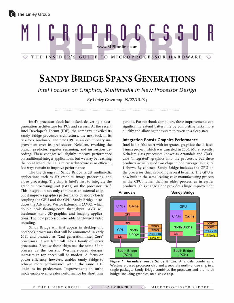
Integration Boosts Graphics Performance Intel had a false start with integrated graphics: the ill-fated Timna project, which was canceled in 2000. More recently, Nehalem-class processors known as Arrandale and Clark-dale “integrated” graphics into the processor, but these products actually used two chips in one package, as Figure 1 shows. By contrast, Sandy Bridge includes the GPU on the processor chip, providing several benefits. The GPU is now built in the same leading-edge manufacturing process as the CPU, rather than an older process, as in earlier products. This change alone provides a huge improvement
Figure 1. Arrandale versus Sandy Bridge. Arrandale combines a Westmere-based processor chip and a separate north-bridge chip in a single package. Sandy Bridge combines the processor and the north bridge, including graphics, on a single chip.
2 Sandy Bridge Spans Generations
SEPTEMBER 2010
in performance per watt, increasing the speed of the shader engines while reducing their power.
The GPU can now access the processor’s large level-three (L3) cache (which Intel now calls the last-level cache, or LLC). When graphics functions executed in a simple pipeline, caching was irrelevant. A modern shader-based architecture, however, can access the same data over and over as it layers one effect over another. The L3 cache short-circuits the path to main memory, providing its in-formation much more quickly. This extra speed improves graphics performance while reducing pressure on the lim-ited DRAM bandwidth.
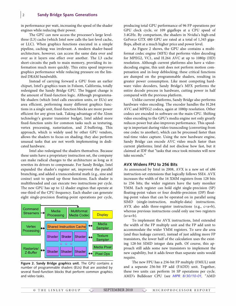
Instead of carrying forward a GPU from an earlier chipset, Intel’s graphics team in Folsom, California, totally redesigned the Sandy Bridge GPU. The biggest change is the amount of fixed-function logic. Although programma-ble shaders (which Intel calls execution units, or EUs) are area efficient, performing many different graphics func-tions in a single unit, fixed-function blocks are more power efficient for any given task. Taking advantage of the 32nm technology’s greater transistor budget, Intel added more fixed-function units for common tasks such as texturing, vertex processing, rasterization, and Z-buffering. This approach, which is widely used by other GPU vendors, allows the shaders to focus on shading; they also perform unusual tasks that are not worth implementing in dedi-cated hardware.
Intel also redesigned the shaders themselves. Because these units have a proprietary instruction set, the company can make radical changes to the architecture as long as it rewrites its drivers to compensate. For Sandy Bridge, Intel expanded the shader’s register set, improved the parallel branching, and added a transcendental math (e.g., sine and cosine) unit to speed up those functions. Each shader is multithreaded and can execute two instructions per cycle. The new GPU has up to 12 shader engines that operate at one-third of the CPU frequency. Each shader can generate eight single-precision floating-point operations per cycle,
producing total GPU performance of 96 FP operations per GPU clock cycle, or 109 gigaflops at a CPU speed of 3.4GHz. By comparison, the shaders in Nvidia’s high-end GeForce GTX 480 GPU are rated at a total of 1,345 giga-flops, albeit at a much higher price and power level.
As Figure 2 shows, the GPU also contains a multi-format codec engine (MFX) that performs video decoding for MPEG2, VC1, and H.264 AVC at up to 1080p (HD) resolution. Although current platforms also have a video-decoding engine, this unit does not perform motion com-pensation and in-loop deblocking; these critical functions are dumped on the programmable shaders, resulting in greater power consumption. Like most competing hard-ware video decoders, Sandy Bridge’s MFX performs the entire decode process in hardware, cutting power in half compared with the previous platform.
Unlike current platforms, Sandy Bridge also performs hardware video encoding. The encoder handles the H.264 AVC and MPEG2 codecs, again at 1080p resolution. Other codecs are encoded in software on the main CPU. Shifting video encoding to the GPU’s media engine not only greatly reduces power but also improves performance. This speed-up is important during video transcoding (converting from one codec to another), which can be processed faster than real-time video capture. Using the new hardware engine, Sandy Bridge can encode AVC video much faster than current platforms; Intel did not disclose how fast, but it claimed at IDF that “tasks that once took minutes will now take seconds.”
AVX Widens FPU to 256 Bits As announced by Intel in 2008, AVX is a new set of x86 instruction-set extensions that logically follows SSE4. AVX increases the width of the 16 XMM registers from 128 bits to 256 bits; the wider registers have the tasty moniker YMM. Each register can hold eight single-precision (SP) floating-point values or four double-precision (DP) float-ing-point values that can be operated on in parallel using SIMD (single-instruction, multiple-data) instructions. AVX also adds three-register instructions (e.g., c=a+b), whereas previous instructions could only use two registers (a=a+b).
To implement the AVX instructions, Intel extended the width of the FP multiply unit and the FP add unit to accommodate the wider YMM registers. To save die area (and thus leakage current), instead of just adding more FP transistors, the lower half of the calculation uses the exist-ing 128-bit SIMD integer data path. Of course, this ap-proach still adds some new transistors to implement the new capability, but it adds fewer than separate units would require.
The new FPU has a 256-bit FP multiply (FMUL) unit and a separate 256-bit FP add (FADD) unit. Together, these two units can perform 16 SP operations per cycle. AMD’s Bulldozer CPU (see MPR 8/30/10-01, “AMD
Figure 2. Sandy Bridge graphics unit. The GPU contains a number of programmable shaders (EUs) that are assisted by several fixed-function blocks that perform common graphics and video tasks.

Sandy Bridge Spans Generations 3
SEPTEMBER 2010
Bulldozer Plows New Ground”) achieves the same level of peak performance in a different way: it provides two 128-bit FP multiply-add (FMA) units that can be combined to execute one 256-bit FMAC instruction per cycle. Sandy Bridge does not implement FMA (which will likely debut in the 2013 Haswell CPU), but it can achieve its peak per-formance on code that uses separate FADD and FMUL instructions. Note that Bulldozer’s peak performance is cut in half when using FADD and FMUL instead of FMA.
Register Files Get Physical To produce the Sandy Bridge CPU in just two years, Intel’s Haifa (Israel) team borrowed heavily from the Nehalem CPU design, following the principle of “if it ain’t broke, don’t fix it.” Implementing AVX, however, broke the reg-ister-renaming method used in Nehalem (and its predeces-sor, Merom, which was also designed by the Haifa team). In these previous CPUs, each instruction stores its source values in the scheduler and its result in the reorder buffer (ROB), which copies the result to the physical register file once the instruction is retired. In-flight instructions must check the ROB (using a content-addressable memory) to locate the most recent copy of any source registers that they require.
Implementing AVX doubles the potential operand size, which could greatly increase the size of both the scheduler and the ROB. Instead, Intel decided to revert to the physical-register scheme used in the old Pentium 4 (and by most RISC processors that implement register renaming). In this method, the CPU implements a rename register file that is much larger than the logical register file. When an instruction is issued, its result is assigned to an unused entry in the rename file. Its source operands are taken from the appropriate rename registers defined by the current mapping. If an exception occurs, the CPU simply replaces the register map with the most recent committed mapping.
This approach eliminates the copying of data from the ROB to the physical register file, saving power. The rename entries for each register file are the same width as that file, so only the YMM rename registers need to be 256 bits wide; using the previous method, every entry in the scheduler and the ROB would have to be able to hold a 256-bit result. As Table 1 shows, this simplification also enabled the team to increase the number of scheduler and ROB entries by 50% and 30%, respectively, increasing the size of the reorder window.
Branch Predictors Get Small The Sandy Bridge team focused on a few other areas to improve the CPU. Because of Nehalem’s long pipeline, accurate branch prediction is critical to its performance. Mispredicted branches not only waste many CPU cycles, they also waste the power used to execute the unneeded instructions. The team wanted to improve the accuracy of
the branch predictor, but without taking a brute-force ap-proach that required more memory and thus more power.
To do so, the team discarded the long-standing wis-dom that a 2-bit predictor is better than a 1-bit predictor. Most branches are, in fact, monotonic, so the 2-bit pre-dictor provides a relatively small improvement in accu-racy—not enough, the team reasoned, to justify the cost and power of the second bit. Put another way, a 2-bit pre-dictor is less accurate than a 1-bit predictor with twice as many entries, yet both use about the same die area and power. Sandy Bridge actually implements slightly more than 1 bit per entry, sharing a single “confidence” bit across several entries to save space and power.
The team then looked at the branch target buffer (BTB), which used 64-bit entries to hold the target ad-dresses. Most branches, however, have very short dis-placements, looping back or jumping forward several in-structions or so. The Sandy Bridge BTB has mostly small entries to hold these offsets, with a few wide entries for long-displacement branches. This change saved so much space that the team was able to double the number of BTB entries and still have room left over. This extra space is used to extend the global branch history, further improv-ing prediction accuracy. As a result, accuracy is improved within about the same die area and power for the branch-prediction unit.
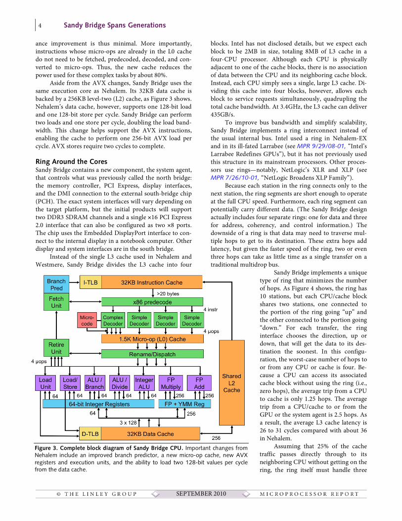
Like Nehalem, Only Better Like Nehalem, Sandy Bridge uses a 32KB instruction cache and decodes four x86 instructions per cycle, converting them into simpler RISC-like micro-ops. A new addition is the micro-op (L0) cache, which can hold 1.5K micro-ops. Assuming an average of 3.5 bytes per x86 instruction, this cache is the equivalent of a 5.25KB instruction cache. Intel claims that the typical hit rate for this cache is about 80%. The L0 cache replaces Nehalem’s loop buffer, which also stores micro-ops but has only 28 entries.
Because instructions already stream from the in-struction cache at the pipeline’s full rate, the new design saves cycles only when execution can be restarted from the L0 cache after a mispredicted branch. The overall perform-
Table 1. Nehalem versus Sandy Bridge. The new CPU design replaces the old physical register file, which contained a sin-gle copy of each logical register, with a new larger set of rename registers. Sandy Bridge also expands the size of the reorder buffer, the scheduler, and the load and store buffers, providing the CPU with greater opportunities to reorder in-structions. (Source: Intel)
Nehalem Sandy Bridge Load Buffers 48 entries 64 entries Store Buffers 32 entries 36 entries Scheduler Entries 36 micro-ops 54 micro-ops Integer Rename File Not applicable 160 registers FP Rename File Not applicable 144 registers Reorder Buffer 128 micro-ops 168 micro-ops
4 Sandy Bridge Spans Generations
SEPTEMBER 2010
ance improvement is thus minimal. More importantly, instructions whose micro-ops are already in the L0 cache do not need to be fetched, predecoded, decoded, and con-verted to micro-ops. Thus, the new cache reduces the power used for these complex tasks by about 80%.
Aside from the AVX changes, Sandy Bridge uses the same execution core as Nehalem. Its 32KB data cache is backed by a 256KB level-two (L2) cache, as Figure 3 shows. Nehalem’s data cache, however, supports one 128-bit load and one 128-bit store per cycle. Sandy Bridge can perform two loads and one store per cycle, doubling the load band-width. This change helps support the AVX instructions, enabling the cache to perform one 256-bit AVX load per cycle. AVX stores require two cycles to complete.
Ring Around the Cores Sandy Bridge contains a new component, the system agent, that controls what was previously called the north bridge: the memory controller, PCI Express, display interfaces, and the DMI connection to the external south-bridge chip (PCH). The exact system interfaces will vary depending on the target platform, but the initial products will support two DDR3 SDRAM channels and a single ×16 PCI Express 2.0 interface that can also be configured as two ×8 ports. The chip uses the Embedded DisplayPort interface to con-nect to the internal display in a notebook computer. Other display and system interfaces are in the south bridge.
Instead of the single L3 cache used in Nehalem and Westmere, Sandy Bridge divides the L3 cache into four
blocks. Intel has not disclosed details, but we expect each block to be 2MB in size, totaling 8MB of L3 cache in a four-CPU processor. Although each CPU is physically adjacent to one of the cache blocks, there is no association of data between the CPU and its neighboring cache block. Instead, each CPU simply sees a single, large L3 cache. Di-viding this cache into four blocks, however, allows each block to service requests simultaneously, quadrupling the total cache bandwidth. At 3.4GHz, the L3 cache can deliver 435GB/s.
To improve bus bandwidth and simplify scalability, Sandy Bridge implements a ring interconnect instead of the usual internal bus. Intel used a ring in Nehalem-EX and in its ill-fated Larrabee (see MPR 9/29/08-01, “Intel’s Larrabee Redefines GPUs”), but it has not previously used this structure in its mainstream processors. Other proces-sors use rings—notably, NetLogic’s XLR and XLP (see MPR 7/26/10-01, “NetLogic Broadens XLP Family”).
Because each station in the ring connects only to the next station, the ring segments are short enough to operate at the full CPU speed. Furthermore, each ring segment can potentially carry different data. (The Sandy Bridge design actually includes four separate rings: one for data and three for address, coherency, and control information.) The downside of a ring is that data may need to traverse mul-tiple hops to get to its destination. These extra hops add latency, but given the faster speed of the ring, two or even three hops can take as little time as a single transfer on a traditional multidrop bus.
Sandy Bridge implements a unique type of ring that minimizes the number of hops. As Figure 4 shows, the ring has 10 stations, but each CPU/cache block shares two stations, one connected to the portion of the ring going “up” and the other connected to the portion going “down.” For each transfer, the ring interface chooses the direction, up or down, that will get the data to its des-tination the soonest. In this configu-ration, the worst-case number of hops to or from any CPU or cache is four. Be-cause a CPU can access its associated cache block without using the ring (i.e., zero hops), the average trip from a CPU to cache is only 1.25 hops. The average trip from a CPU/cache to or from the GPU or the system agent is 2.5 hops. As a result, the average L3 cache latency is 26 to 31 cycles compared with about 36 in Nehalem.
Assuming that 25% of the cache traffic passes directly through to its neighboring CPU without getting on the ring, the ring itself must handle three
Figure 3. Complete block diagram of Sandy Bridge CPU. Important changes from Nehalem include an improved branch predictor, a new micro-op cache, new AVX registers and execution units, and the ability to load two 128-bit values per cycle from the data cache.

Sandy Bridge Spans Generations 5
SEPTEMBER 2010
transactions per cycle to sustain the remaining cache band-width. That means, on average, either the up or down leg must handle two transactions at once, which may be diffi-cult to schedule. Thus, the ring may not be able to sustain the full bandwidth of the caches, but it will provide much greater bandwidth than Nehalem’s internal bus.
The architecture easily scales downward by removing two of the CPUs and their associated cache blocks. This change reduces both the size and bandwidth of the L3 cache to match the reduction in CPU count. With only two cache blocks, the ring can sustain the full cache bandwidth. Alternatively, the architecture can be extended to eight or more CPUs. In this case, Intel could double the ring width to 512 bits to help support the greater bandwidth of the additional cache blocks.
Figure 5 shows a die photo of the chip in which the six ring stations can clearly be seen. Intel did not disclose the die size of the chip, but it is said to be about 225mm2. The graphics and video unit at the bottom of the chip takes 20% of the total die area. This unit appears to consist mainly of synthesized logic, whereas the CPUs and caches use custom circuit design to maximize performance. The north-bridge logic, not counting the I/O drivers, is only 8% of the die. The four CPUs together use 33% of the die, making them just under 20mm2 each. The 8MB of L3 cache (L3$) covers 20% of the die. Most of the I/O drivers are for the two 64-bit channels of DDR3 SDRAM. Note that removing two of the CPUs and two of the cache blocks would reduce the total die area by about 30%.
Revving Up Turbo Mode As with Intel’s other multicore processors, the frequency of each CPU core can be adjusted individually, so it can be
turned on or off as needed. Even when its clock is turned off, however, the CPU burns leakage power. So, when the processor is truly idle, the voltage to the CPUs can be turned off, completely eliminating their power dissipation. The graphics unit is on a separate voltage plane, so it can be disabled for applications that do not require graphics. The system agent and north-bridge logic are on a third power plane, which allows the north bridge to refresh the display while the rest of the processor is asleep.
The system agent contains the power manager—a programmable microcontroller that controls the power state of all units and controls reset functions. This ap-proach allows power-management decisions to be made more quickly than by running a driver on one of the CPUs.
If only one Nehalem CPU is active, it is allowed to exceed its rated speed, since even at a higher speed, one CPU will not exceed the multicore chip’s total TDP budget. Intel calls this feature turbo boost. Sandy Bridge takes a different view of turbo boost, focusing on die temperature rather than instantaneous power dissipation.
Consider a processor that has been sitting idle for several seconds; perhaps the user is considering what digi-tal effect to apply to a photograph. The processor and its thermal system (e.g., heat sink) will cool down. If the user
Figure 5. Sandy Bridge die photo with overlay. The red boxes show the ring stations. The 12 shaders (EUs) can be seen at the lower left. (Source: photo by Intel, overlay by The Linley Group)
Figure 4. High-level block diagram of Sandy Bridge. The L3 cache is divided into four blocks, which are connected to the four CPU cores, the GPU, and the system agent through a ring interconnect.
6 Sandy Bridge Spans Generations
SEPTEMBER 2010
then begins a CPU-intensive activity, the entire processor can operate well above its rated TDP for quite some time (up to 25 seconds, Intel claims) while the thermal system heats back up. Once the chip reaches its maximum oper-ating temperature, it must throttle back to its rated TDP level to avoid overheating.
Sandy Bridge’s power manager estimates the chip’s temperature and calculates the degree and duration of the turbo boost. In this design, the maximum CPU speed in turbo mode is limited only by the physical speed of the transistors and the current that can be supplied to the chip. Turbo mode should be particularly effective in mobile Sandy Bridge chips, since these chips have more head-room. Because the chip does not physically measure its own temperature, the power manager estimates the tem-perature on the basis of recent workloads and the thermal characteristics of the device and its cooling system. Pre-sumably, Intel has built in a safety factor, but any unau-thorized or even unintentional modification of the cooling system could wreak havoc with the power manager’s cal-culations.
The integration of GPU and CPUs on one chip cre-ates additional turbo opportunities. If the GPU is not in use or is operating at a low speed, the power manager can assign some of its thermal budget to the CPUs, allowing them to run at a higher clock speed. Conversely, on a graphics-intensive application, the power manager can overclock the GPU while slowing down the CPUs.
Turbo mode should provide a noticeable speedup to PC users—up to 40% in some situations. Users who often leave their system idle or in a low-power state before launching a brief burst of computation will particularly benefit. Gamers or professional users who execute long CPU-intensive jobs will not see as much gain. Bench-marking a Sandy Bridge processor could generate widely different results depending on how the test is run. Intel recommends allowing the processor to rest quietly for a
moment before running each benchmark, but this ap-proach may not be indicative of real-world usage.
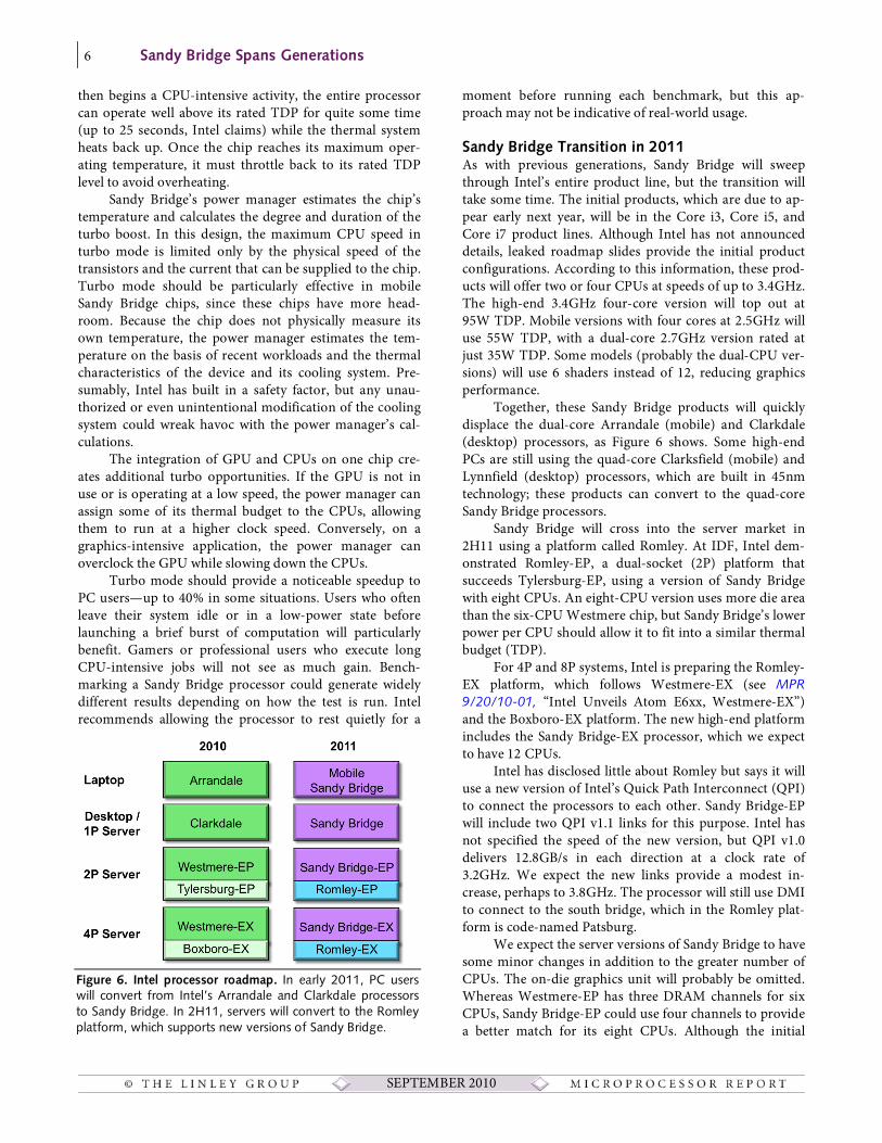
Sandy Bridge Transition in 2011 As with previous generations, Sandy Bridge will sweep through Intel’s entire product line, but the transition will take some time. The initial products, which are due to ap-pear early next year, will be in the Core i3, Core i5, and Core i7 product lines. Although Intel has not announced details, leaked roadmap slides provide the initial product configurations. According to this information, these prod-ucts will offer two or four CPUs at speeds of up to 3.4GHz. The high-end 3.4GHz four-core version will top out at 95W TDP. Mobile versions with four cores at 2.5GHz will use 55W TDP, with a dual-core 2.7GHz version rated at just 35W TDP. Some models (probably the dual-CPU ver-sions) will use 6 shaders instead of 12, reducing graphics performance.
Together, these Sandy Bridge products will quickly displace the dual-core Arrandale (mobile) and Clarkdale (desktop) processors, as Figure 6 shows. Some high-end PCs are still using the quad-core Clarksfield (mobile) and Lynnfield (desktop) processors, which are built in 45nm technology; these products can convert to the quad-core Sandy Bridge processors.
Sandy Bridge will cross into the server market in 2H11 using a platform called Romley. At IDF, Intel dem-onstrated Romley-EP, a dual-socket (2P) platform that succeeds Tylersburg-EP, using a version of Sandy Bridge with eight CPUs. An eight-CPU version uses more die area than the six-CPU Westmere chip, but Sandy Bridge’s lower power per CPU should allow it to fit into a similar thermal budget (TDP).
For 4P and 8P systems, Intel is preparing the Romley-EX platform, which follows Westmere-EX (see MPR 9/20/10-01, “Intel Unveils Atom E6xx, Westmere-EX”) and the Boxboro-EX platform. The new high-end platform includes the Sandy Bridge-EX processor, which we expect to have 12 CPUs.
Intel has disclosed little about Romley but says it will use a new version of Intel’s Quick Path Interconnect (QPI) to connect the processors to each other. Sandy Bridge-EP will include two QPI v1.1 links for this purpose. Intel has not specified the speed of the new version, but QPI v1.0 delivers 12.8GB/s in each direction at a clock rate of 3.2GHz. We expect the new links provide a modest in-crease, perhaps to 3.8GHz. The processor will still use DMI to connect to the south bridge, which in the Romley plat-form is code-named Patsburg.
We expect the server versions of Sandy Bridge to have some minor changes in addition to the greater number of CPUs. The on-die graphics unit will probably be omitted. Whereas Westmere-EP has three DRAM channels for six CPUs, Sandy Bridge-EP could use four channels to provide a better match for its eight CPUs. Although the initial
Figure 6. Intel processor roadmap. In early 2011, PC users will convert from Intel’s Arrandale and Clarkdale processors to Sandy Bridge. In 2H11, servers will convert to the Romley platform, which supports new versions of Sandy Bridge.

Sandy Bridge Spans Generations 7
SEPTEMBER 2010
Sandy Bridge processors will integrate PCI Express 2.0, the server versions provide a good opportunity for Intel to debut the faster PCI Express 3.0. The new specification, which is due to be completed in late 2010, doubles PCI Express throughput to 8Gbps per lane, or 16GB/s for a 16-lane slot.
Intel has already taped out its first 22nm processor. Following the tick-tock plan, Ivy Bridge is a 22nm shrink of Sandy Bridge that is scheduled to enter production in late 2011. As a “tick,” Ivy Bridge is not expected to add many new features to the platform, but the 22nm process will significantly reduce power per CPU and enable Intel to put more CPUs on a chip. Following Ivy Bridge is Haswell, the next tock. Little is known about Haswell, but it is said to be a completely new CPU microarchitecture.
Intel Steamrolls Bulldozer AMD “coincidentally” disclosed its next-generation Bull-dozer architecture just one month before Intel disclosed Sandy Bridge. Thus, it is natural to compare the two de-signs. Although AMD has beefed up its microarchitecture, Bulldozer matches up better against Nehalem/Westmere than it does against Sandy Bridge, as Table 2 shows. Intel has again upped the ante by expanding the reorder capa-bilities of its CPU. Sandy Bridge’s micro-op cache is a unique feature that offers performance and power-savings opportunities. We also suspect Intel’s branch prediction is superior, although neither vendor has disclosed enough information to be sure. Bulldozer’s 16KB data cache may also hinder it on certain single-thread applications.
On dual-threaded applications, Bulldozer’s unique two-core module offers clear benefits over Intel’s Hyper-Threading design. Sandy Bridge must share its execution units and reorder buffer between the two threads, whereas Bulldozer offers each thread a separate set of resources. But AMD counts each Bulldozer module as two cores, so all we can say is that two Bulldozer cores are better than one Sandy Bridge.
Although AMD has been talking about in-tegrating graphics for years, Intel has actually been doing it, first with the two-chip module of Arrandale and Clarkdale and then with the sin-gle-die Sandy Bridge. AMD’s first Fusion chip, code-named Ontario (see MPR 8/30/10-02, “Bobcat Snarls at Atom”), is scheduled to debut in 4Q10, only slightly before Sandy Bridge. We do not expect the first Bulldozer processors to integrate graphics. Sandy Bridge should negate any gains AMD might have achieved from its Fusion project.
Sandy Bridge products will appear in early 2011, whereas we expect the first Bulldozer products to ship in mid-2011. Although this schedule gives Sandy Bridge a head start of sev-eral months in the desktop and mobile markets,
Bulldozer is headed straight for the server market in the Valencia and Interlagos processors. Thus, Bulldozer may actually appear in servers before Sandy Bridge does (in the Romley platform).
Whereas Sandy Bridge is the clear winner on a core-to-core basis, a Bulldozer core will use much less power, allowing AMD to operate Valencia at a higher clock speed within the same thermal envelope. Sandy Bridge-EP should handily outperform Valencia on SPECint per watt, although the Bulldozer chip may narrow the gap from cur-rent products.
Rising to the Next Level Sandy Bridge brings several architectural innovations to Intel’s platforms. PC users will see the biggest improve-ments in multimedia performance, particularly video encoding but also graphics and image processing. On these types of applications, which are becoming increasingly popular, users will see an improvement of 2× or better compared with Intel’s previous graphics solutions.
The CPU microarchitecture improvements are fairly subtle, given the evolutionary design approach. We expect performance per megahertz to improve very modestly, perhaps by 10% on most applications. Many of the design changes, particularly the L0 micro-op cache, aim to reduce power more than to increase performance. Intel has not quantified these gains, but we estimate they could trim CPU power by 10% at the same clock speed. Because most of the company’s products are power limited, Intel can turn power efficiency into higher clock speeds at the same TDP levels, providing an effective performance boost of 20% for Sandy Bridge compared with Westmere. In certain situations, the improved turbo boost will magnify this gain by as much as 40%, which can translate directly into longer battery life for notebook computers.
AMD Bulldozer
Intel Westmere
Intel Sandy Bridge
Building Block Dual CPU CPU core CPU core Integrated Graphics? Not disclosed In package On chip Instruction Extensions SSE1–SSE4.2,
AES, AVX SSE1–SSE4.2,
AES SSE1–SSE4.2,
AES, AVX Number of Threads 2 threads 2 threads 2 threads Instr Decode Rate 4 per cycle 4 per cycle 4 per cycle Micro-Op Issue Rate 4 per cycle* 4 per cycle 4 per cycle Instr Reordering 128 micro-ops* 128 micro-ops 168 micro-ops FP Operations (SP) 16 per cycle 8 per cycle 16 per cycle L0 (micro-op) Cache None None 1.5K micro-ops L1 Cache (I/D) 64KB/16KB† 32KB/32KB 32KB/32KB L2 Cache Undisclosed 256KB 256KB IC Process 32nm 32nm 32nm First Production Mid-2011‡ Early 2010 Early 2011
Table 2. Comparison of AMD Bulldozer and Intel Sandy Bridge CPUs. Greater instruction reordering and an L0 cache should improve Sandy Bridge’s performance over Bulldozer’s. *Dedicated amount for each thread; †L1 data cache dedicated for each thread. (Source: vendors, ex-cept ‡The Linley Group estimate)
8 Sandy Bridge Spans Generations
SEPTEMBER 2010
The integration of graphics has several effects. It in-creases performance while greatly reducing power: we ex-pect a performance gain of about 2× at one-fifth the power compared with the Arrandale/Clarkdale graphics unit. Integration is likely to reduce manufacturing cost com-pared with the current two-chip module (or with an exter-nal GPU chip). Graphics integration also makes PC makers less likely to choose a third-party graphics solution. Al-though the performance of Intel’s graphics has generally been modest at best, the improvement in Sandy Bridge makes it acceptable for most PC users. Gamers and others who care about maximizing graphics performance will still opt for an external graphics card.
Intel’s rollout schedule brings Sandy Bridge to the PC market in early 2011, but it will not reach the server market until late that year. In targeting the PC market first, Intel satisfies the bulk of its customer base and should extend its lead over AMD in PCs. But AMD’s focus on the server market may allow Bulldozer to beat Sandy Bridge to that market. Furthermore, AMD’s strategy of making Bulldozer a smaller, lighter core may prove more power efficient than Intel’s bulkier Sandy Bridge. AMD has been successful with server customers by undercutting Intel on price; Bull-dozer may provide it with an additional advantage in that market.
Intel’s track record of bringing new processor archi-tectures to market is impressive and unrivaled. No other processor vendor can completely remake its product line on an annual basis, yet Intel has done just that in each of the past four years. With Sandy Bridge, the company is poised to go five for five. The new processor shows that Intel is thinking outside of the CPU box, delivering new graphics and multimedia capabilities to support emerging usage models. Taking advantage of the growing transistor budget provided by its industry-leading fab technology, the company is integrating new features along with additional system functions, improving efficiency. Sandy Bridge will carry Intel into the next generation of PCs. ♦
For More Information
Intel has not yet announced any products using the Sandy Bridge architecture. We expect the first Sandy Bridge products to ship in early 2011. For more informa-tion on Sandy Bridge, download Intel’s IDF presentations from www.intel.com/go/idfsessions (search for Sandy Bridge). For complete information on the AVX exten-sions, access http://software.intel.com/en-us/avx.
To subscribe to Microprocessor Report, access www.MPRonline.com or phone us at 408-945-3943.
Related Documents