Analytical TEM study of CVD diamond growth on TiO 2 sol–gel layers Ying-Gang Lu a, ⁎, Johan Verbeeck a , Stuart Turner a , An Hardy b, c , Stoffel D. Janssens b, c , Christopher De Dobbelaere b , Patrick Wagner b, c , Marlies K. Van Bael b, c , Ken Haenen b, c , Gustaaf Van Tendeloo a a EMAT, University of Antwerp Groenenborgerlaan 171, B-2020 Antwerp, Belgium b Institute for Materials Research (IMO), Hasselt University, B-3950 Diepenbeek, Belgium c IMEC vzw, IMOMEC, B-3590 Diepenbeek, Belgium abstract article info Article history: Received 9 November 2011 Received in revised form 13 January 2012 Accepted 19 January 2012 Available online 26 January 2012 Keywords: Diamond film Plasma CVD Diffusion High resolution electron microscopy The early growth stages of chemical vapor deposition (CVD) diamond on a sol–gel TiO 2 film with buried ultra dispersed diamond seeds (UDD) have been studied. In order to investigate the diamond growth mechanism and understand the role of the TiO 2 layer in the growth process, high resolution transmission electron microscopy (HRTEM), energy-filtered TEM and electron energy loss spectroscopy (EELS) techniques were applied to cross sectional diamond film samples. We find evidence for the formation of TiC crystallites inside the TiO 2 layer at different diamond growth stages. However, there is no evidence that diamond nucleation starts from these crystallites. Carbon diffusion into the TiO 2 layer and the chemical bonding state of carbon (sp 2 /sp 3 ) were both extensively investigated. We provide evidence that carbon diffuses through the TiO 2 layer and that the diamond seeds partially convert to amor- phous carbon during growth. This carbon diffusion and diamond to amorphous carbon conversion make the seed areas below the TiO 2 layer grow and bend the TiO 2 layer upwards to form the nucleation center of the diamond film. In some of the protuberances a core of diamond seed remains, covered by amorphous carbon. It is however unlikely that the remaining seeds are still active during the growth process. Crown Copyright © 2012 Published by Elsevier B.V. All rights reserved. 1. Introduction The development of chemical vapor deposition (CVD) techniques has allowed the outstanding properties of diamond films to be used in a wide field of technological applications [1–5]. Previous studies have demonstrated that when titanium surfaces are modified with a TiO 2 layer, the biocompatibility and the extent of bone-implant tolerance is increased [6–8]. Combining the outstanding properties of diamond films with the excellent biocompatibility of TiO 2 layers in biomedical applications is an attractive prospect [9,10]. Most of these applications only require a very thin layer of nanocrystalline diamond and, as a consequence, the nucleation of such films need to be fully understood to guarantee thin, closed and conformal layers on 3D structures [11–14]. To realize this type of applications, dia- mond coatings must be produced to a high standard and with prede- termined properties, which will only be possible if their nucleation and growth mechanism are thoroughly understood. Due to the high surface energy of diamond, its nucleation on non-diamond substrates is characterized by low nucleation densities and long incubation times. Consequently, surface pretreatment is commonly needed. Usually, diamond nucleation is enhanced by treating substrates by means of mechanical abrasion with diamond powder, or a mixture of diamond and other hard powders (such as Ti, Al 2 O 3 etc.) [15–17], or by so-called bias enhanced nucleation (BEN) [18,19]. Mechanical treatments are simple and effective, but limited to planar surfaces, while BEN requires the substrate to be conductive. Both techniques can cause surface damage and contamination. Direct seeding with colloidal ultra dispersed diamond (UDD) is an effective solution to these problems and simultaneously enhances the diamond nucle- ation [20]. Besides mechanical abrasion, BEN or colloidal seeding, inter- layer materials are widely used to enhance diamond nucleation and diamond film adhesion to substrates. Among others, interlayer materials like W, Ti, Zr and Ni/Cu/Ti multilayers [21,22] or inter- mediate layers [23] are employed to obtain adherent diamond coating on steel and WC–Co. Titanium is known to be a getter ma- terial that easily forms carbides and improves carbon adhesion to the growth interface. Carbon diffusion is also crucial for diamond nucleation and growth. The interface material plays an important role in the diffusion process of carbon. Previous studies have indi- cated that high quality diamond films can be grown on UDD seeds buried under a sol–gel TiO 2 layer [4]. However, mapping of the amorphous carbon distribution on diamond was not performed in these investigations. Diamond & Related Materials 23 (2012) 93–99 ⁎ Corresponding author. Tel.: + 32 32653331; fax: + 32 3265 33 18. E-mail address: [email protected] (Y.-G. Lu). 0925-9635/$ – see front matter. Crown Copyright © 2012 Published by Elsevier B.V. All rights reserved. doi:10.1016/j.diamond.2012.01.022 Contents lists available at SciVerse ScienceDirect Diamond & Related Materials journal homepage: www.elsevier.com/locate/diamond

Welcome message from author
This document is posted to help you gain knowledge. Please leave a comment to let me know what you think about it! Share it to your friends and learn new things together.
Transcript
Diamond & Related Materials 23 (2012) 93–99
Contents lists available at SciVerse ScienceDirect
Diamond & Related Materials
j ourna l homepage: www.e lsev ie r .com/ locate /d iamond
Analytical TEM study of CVD diamond growth on TiO2 sol–gel layers
Ying-Gang Lu a,⁎, Johan Verbeeck a, Stuart Turner a, An Hardy b,c, Stoffel D. Janssens b,c,Christopher De Dobbelaere b, Patrick Wagner b,c, Marlies K. Van Bael b,c,Ken Haenen b,c, Gustaaf Van Tendeloo a
a EMAT, University of Antwerp Groenenborgerlaan 171, B-2020 Antwerp, Belgiumb Institute for Materials Research (IMO), Hasselt University, B-3950 Diepenbeek, Belgiumc IMEC vzw, IMOMEC, B-3590 Diepenbeek, Belgium
⁎ Corresponding author. Tel.: +32 32653331; fax: +E-mail address: [email protected] (Y.-G. Lu).
0925-9635/$ – see front matter. Crown Copyright © 20doi:10.1016/j.diamond.2012.01.022
a b s t r a c t
a r t i c l e i n f oArticle history:Received 9 November 2011Received in revised form 13 January 2012Accepted 19 January 2012Available online 26 January 2012
Keywords:Diamond filmPlasma CVDDiffusionHigh resolution electron microscopy
The early growth stages of chemical vapor deposition (CVD) diamond on a sol–gel TiO2 film with buried ultradispersed diamond seeds (UDD) have been studied. In order to investigate the diamond growth mechanismand understand the role of the TiO2 layer in the growth process, high resolution transmission electronmicroscopy (HRTEM), energy-filtered TEM and electron energy loss spectroscopy (EELS) techniques wereapplied to cross sectional diamond film samples.We find evidence for the formation of TiC crystallites inside the TiO2 layer at different diamond growth stages.However, there is no evidence that diamond nucleation starts from these crystallites. Carbon diffusion into theTiO2 layer and the chemical bonding state of carbon (sp2/sp3) were both extensively investigated. We provideevidence that carbon diffuses through the TiO2 layer and that the diamond seeds partially convert to amor-phous carbon during growth. This carbon diffusion and diamond to amorphous carbon conversion make theseed areas below the TiO2 layer grow and bend the TiO2 layer upwards to form the nucleation center of thediamond film. In some of the protuberances a core of diamond seed remains, covered by amorphous carbon.It is however unlikely that the remaining seeds are still active during the growth process.
Crown Copyright © 2012 Published by Elsevier B.V. All rights reserved.
1. Introduction
The development of chemical vapor deposition (CVD) techniqueshas allowed the outstanding properties of diamond films to be usedin a wide field of technological applications [1–5]. Previous studieshave demonstrated that when titanium surfaces are modified witha TiO2 layer, the biocompatibility and the extent of bone-implanttolerance is increased [6–8]. Combining the outstanding propertiesof diamond films with the excellent biocompatibility of TiO2 layersin biomedical applications is an attractive prospect [9,10]. Most ofthese applications only require a very thin layer of nanocrystallinediamond and, as a consequence, the nucleation of such films needto be fully understood to guarantee thin, closed and conformal layerson 3D structures [11–14]. To realize this type of applications, dia-mond coatings must be produced to a high standard and with prede-termined properties, which will only be possible if their nucleationand growth mechanism are thoroughly understood. Due to the highsurface energy of diamond, its nucleation on non-diamond substratesis characterized by low nucleation densities and long incubationtimes. Consequently, surface pretreatment is commonly needed.
32 3265 33 18.
12 Published by Elsevier B.V. All rig
Usually, diamond nucleation is enhanced by treating substrates bymeans of mechanical abrasion with diamond powder, or a mixtureof diamond and other hard powders (such as Ti, Al2O3 etc.) [15–17],or by so-called bias enhanced nucleation (BEN) [18,19]. Mechanicaltreatments are simple and effective, but limited to planar surfaces,while BEN requires the substrate to be conductive. Both techniquescan cause surface damage and contamination. Direct seeding withcolloidal ultra dispersed diamond (UDD) is an effective solution tothese problems and simultaneously enhances the diamond nucle-ation [20].
Besides mechanical abrasion, BEN or colloidal seeding, inter-layer materials are widely used to enhance diamond nucleationand diamond film adhesion to substrates. Among others, interlayermaterials like W, Ti, Zr and Ni/Cu/Ti multilayers [21,22] or inter-mediate layers [23] are employed to obtain adherent diamondcoating on steel and WC–Co. Titanium is known to be a getter ma-terial that easily forms carbides and improves carbon adhesion tothe growth interface. Carbon diffusion is also crucial for diamondnucleation and growth. The interface material plays an importantrole in the diffusion process of carbon. Previous studies have indi-cated that high quality diamond films can be grown on UDD seedsburied under a sol–gel TiO2 layer [4]. However, mapping of theamorphous carbon distribution on diamond was not performedin these investigations.
hts reserved.
(a)
(b)
untreated
10 mins
10n m
20n m
diamond a-C Ti
diamond a-C Ti
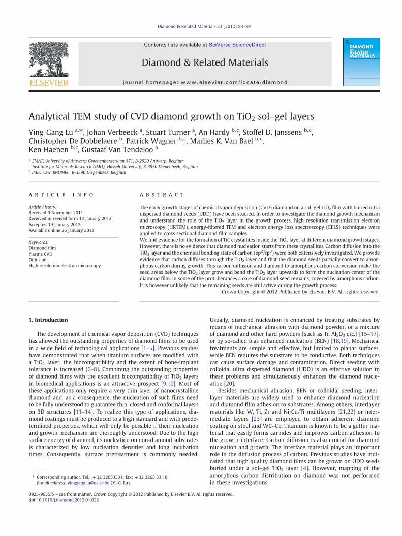
Fig. 1. Elemental maps from model-based EELS data fitting, a: untreated sample;b: 10 min H2+CH4 treated sample.
94 Y.-G. Lu et al. / Diamond & Related Materials 23 (2012) 93–99
In order to further understand the influence of the TiO2 layeron diamond film growth and gain insight into the carbon diffusionprocess, we investigated the early growth stages of a nanocrystallinediamond film prepared by CVD on top of sol–gel TiO2 layers withunderlying UDD seeds on a silicon substrate. The growth stages,carbon diffusion, presence of diamond and amorphous carbon, thestability of the diamond seeds and Ti diffusion phenomena are stud-ied by analytical TEM techniques.
2. Experimental
Si substrates were cleaned with sulfuric acid/hydrogen peroxideand ammonia/hydrogen peroxide mixtures (SPM and APM, respec-tively), followed by an immersion for a few seconds into an aqueouscolloid with nanodiamond particles of ≈10 nm in size [20]. The det-onation nanodiamond powder was obtained from the NanoCarbonInstitute Co., Ltd., Japan. After dispersion in water using an ultrasonichorn, no further surface treatments of the particles was done. Subse-quently sol–gel nominal TiO2 was deposited on these seeded sub-strates by spin-coating (3000 min−1, 30 s). The precursor used wasan aqueous citratoperoxo-Ti solution (pH=7, 0.09 mol L−1) synthe-sized as reported previously [24]. Thermal treatment was carriedout on hot plates (260 °C/2 min and 450 °C/2 min). Films consistedof two layers to obtain a total thickness of approximately 10 nm.The microwave plasma enhanced (MWPE) CVD growth was carriedout in an ASTeX 6500 deposition system [25]. Typical growth condi-tions used were as follows: H2 and CH4 gas flows were 485 sccmand 15 sccm, respectively. The plasma was sustained by 3500 W mi-crowave power at a process pressure of 25 Torr, while the substratetemperature was 630 °C.
In order to investigate the different stages of early diamond filmnucleation, the CVD reaction was interrupted at different growthtimes of 5, 10 and 20 min. A pure hydrogen plasma exposure series,using similar experimental conditions but without CH4 was also per-formed in order to investigate the possible role of H2 and its radicalson the sol–gel layer.
Cross-sectional TEM samples were prepared by focused ion beam(FIB) etching from bulk samples. In order to protect the diamond par-ticles, a gold or chromium protection layer was deposited on top ofthe diamond layer prior to FIB preparation. High angle annular darkfield (HAADF) images and EELS spectra were acquired using an aber-ration corrected FEI Titan 80–300 “cube” microscope operated inscanning transmission electron microscopy (STEM) mode equippedwith a GIF Quantum spectrometer. The convergence semi-angleused was 18.5 mrad, and the acceptance angle was ~200 mrad. Themicroscope was operated at 120 kV in order to reduce knock-on dam-age by the electron beam. High resolution images and energy filteredTEM (EFTEM) images were recorded using JEOL-3000F operating at300 kV equipped with GIF 2000 electron energy loss spectrometer[26]. The STEM-EELS spectra were quantified by multiple leastsquares fitting to reference spectra of the C K-edge for diamond,amorphous carbon and TiC [27].
3. Results and discussions
3.1. Nucleation and growth process
As stated above, samples were grown with CVD growth times of 5,10 and 20 min in order to investigate the different stages of earlydiamond film nucleation. Fig. 1 depicts the distribution of chemicalelements during the different stages of growth (oxygen map notshown). Fig. 1. (a) shows the sample after sol–gel deposition of theTiO2 buffer layer (no plasma treatment) and Fig. 1 (b) shows a similarsample after 10 min of growth in a mixed H2/CH4 plasma.
The untreated sample in Fig. 1 (a) shows (from top to bottom) theamorphous carbon layer, the sol–gel TiO2 buffer layer and some
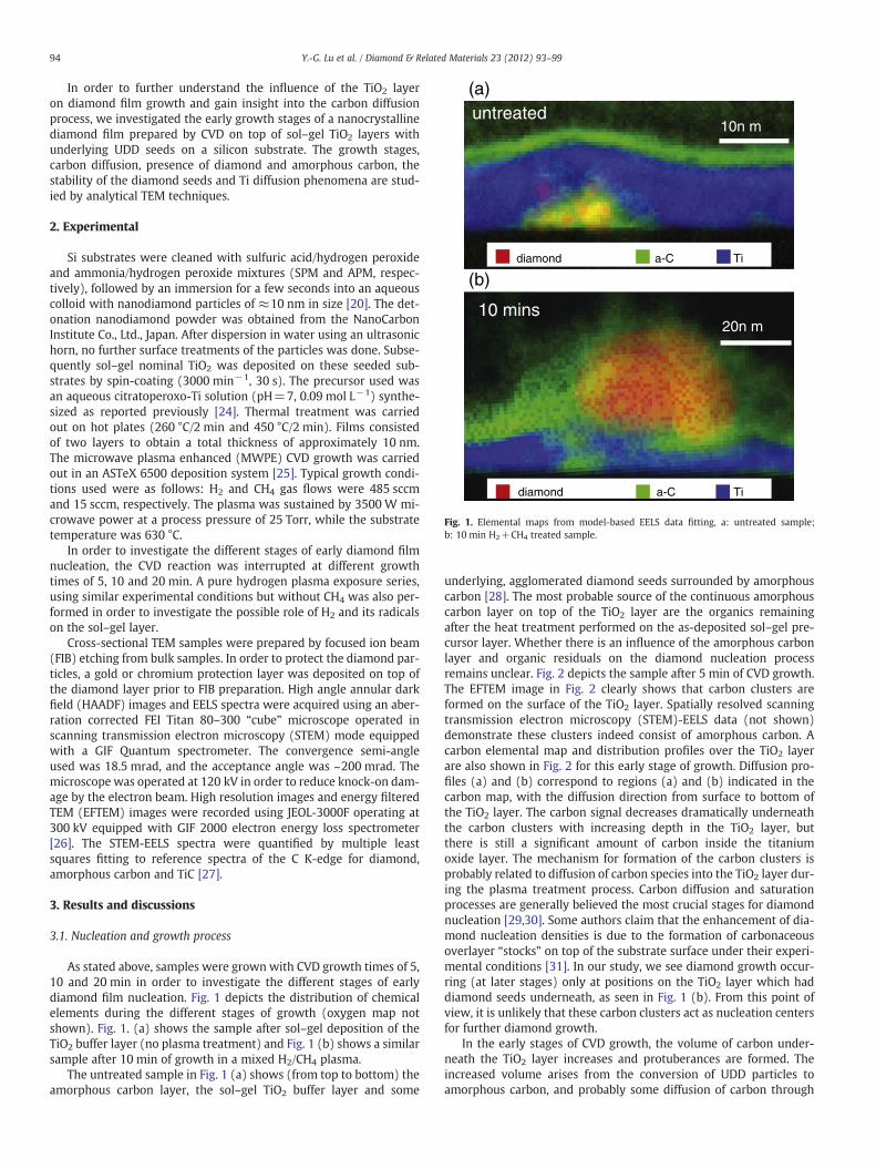
underlying, agglomerated diamond seeds surrounded by amorphouscarbon [28]. The most probable source of the continuous amorphouscarbon layer on top of the TiO2 layer are the organics remainingafter the heat treatment performed on the as-deposited sol–gel pre-cursor layer. Whether there is an influence of the amorphous carbonlayer and organic residuals on the diamond nucleation processremains unclear. Fig. 2 depicts the sample after 5 min of CVD growth.The EFTEM image in Fig. 2 clearly shows that carbon clusters areformed on the surface of the TiO2 layer. Spatially resolved scanningtransmission electron microscopy (STEM)-EELS data (not shown)demonstrate these clusters indeed consist of amorphous carbon. Acarbon elemental map and distribution profiles over the TiO2 layerare also shown in Fig. 2 for this early stage of growth. Diffusion pro-files (a) and (b) correspond to regions (a) and (b) indicated in thecarbon map, with the diffusion direction from surface to bottom ofthe TiO2 layer. The carbon signal decreases dramatically underneaththe carbon clusters with increasing depth in the TiO2 layer, butthere is still a significant amount of carbon inside the titaniumoxide layer. The mechanism for formation of the carbon clusters isprobably related to diffusion of carbon species into the TiO2 layer dur-ing the plasma treatment process. Carbon diffusion and saturationprocesses are generally believed the most crucial stages for diamondnucleation [29,30]. Some authors claim that the enhancement of dia-mond nucleation densities is due to the formation of carbonaceousoverlayer “stocks” on top of the substrate surface under their experi-mental conditions [31]. In our study, we see diamond growth occur-ring (at later stages) only at positions on the TiO2 layer which haddiamond seeds underneath, as seen in Fig. 1 (b). From this point ofview, it is unlikely that these carbon clusters act as nucleation centersfor further diamond growth.
In the early stages of CVD growth, the volume of carbon under-neath the TiO2 layer increases and protuberances are formed. Theincreased volume arises from the conversion of UDD particles toamorphous carbon, and probably some diffusion of carbon through
(a) (b)
50n m Carbon map
5mins
O Ti
50 nm
(a) (b)
coun
ts (
a.u)
coun
ts (
a.u)
Distance (nm) Distance (nm)
C
Fig. 2. EFTEM images showing carbon distribution of the 5 min H2/CH4 treated sample. (a) and (b) are diffusion profiles across regions a and b.
95Y.-G. Lu et al. / Diamond & Related Materials 23 (2012) 93–99
the TiO2 layer. This effect leads to an increase in volume of the protu-berances with increasing plasma exposure time. Simple volumetriccalculations demonstrate that the increase in protuberance volumecan largely be explained by the UDD diamond to amorphous carbonconversion.
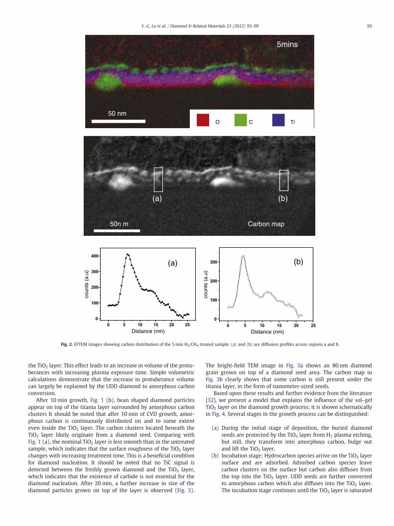
After 10 min growth, Fig. 1 (b), bean shaped diamond particlesappear on top of the titania layer surrounded by amorphous carbonclusters It should be noted that after 10 min of CVD growth, amor-phous carbon is continuously distributed on and to some extenteven inside the TiO2 layer. The carbon clusters located beneath theTiO2 layer likely originate from a diamond seed. Comparing withFig. 1 (a), the nominal TiO2 layer is less smooth than in the untreatedsample, which indicates that the surface roughness of the TiO2 layerchanges with increasing treatment time. This is a beneficial conditionfor diamond nucleation. It should be noted that no TiC signal isdetected between the freshly grown diamond and the TiO2 layer,which indicates that the existence of carbide is not essential for thediamond nucleation. After 20 min, a further increase in size of thediamond particles grown on top of the layer is observed (Fig. 3).
The bright-field TEM image in Fig. 3a shows an 80 nm diamondgrain grown on top of a diamond seed area. The carbon map inFig. 3b clearly shows that some carbon is still present under thetitania layer, in the form of nanometer-sized seeds.
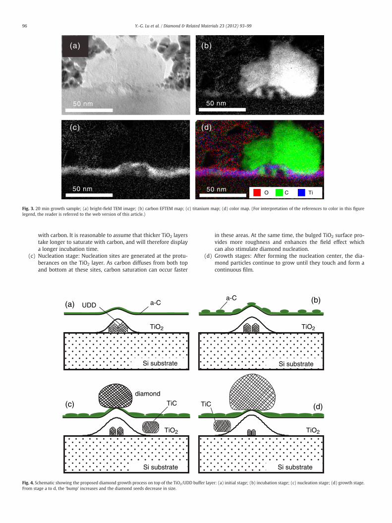
Based upon these results and further evidence from the literature[32], we present a model that explains the influence of the sol–gelTiO2 layer on the diamond growth process; it is shown schematicallyin Fig. 4. Several stages in the growth process can be distinguished:
(a) During the initial stage of deposition, the buried diamondseeds are protected by the TiO2 layer from H2 plasma etching,but still, they transform into amorphous carbon, bulge outand lift the TiO2 layer.
(b) Incubation stage: Hydrocarbon species arrive on the TiO2 layersurface and are adsorbed. Adsorbed carbon species leavecarbon clusters on the surface but carbon also diffuses fromthe top into the TiO2 layer. UDD seeds are further convertedto amorphous carbon which also diffuses into the TiO2 layer.The incubation stage continues until the TiO2 layer is saturated
50 nm 50 nm
50 nm50 nmO Ti
(d)(c)
(b)(a)
C
Fig. 3. 20 min growth sample; (a) bright-field TEM image; (b) carbon EFTEM map; (c) titanium map; (d) color map. (For interpretation of the references to color in this figurelegend, the reader is referred to the web version of this article.)
96 Y.-G. Lu et al. / Diamond & Related Materials 23 (2012) 93–99
with carbon. It is reasonable to assume that thicker TiO2 layerstake longer to saturate with carbon, and will therefore displaya longer incubation time.
(c) Nucleation stage: Nucleation sites are generated at the protu-berances on the TiO2 layer. As carbon diffuses from both topand bottom at these sites, carbon saturation can occur faster
(a)
Si substrateSi substrate
(c)
a-C
TiC
diamond
UDD
Si substrate
TiO2
TiO2
Fig. 4. Schematic showing the proposed diamond growth process on top of the TiO2/UDD buFrom stage a to d, the ‘bump’ increases and the diamond seeds decrease in size.
in these areas. At the same time, the bulged TiO2 surface pro-vides more roughness and enhances the field effect whichcan also stimulate diamond nucleation.
(d) Growth stages: After forming the nucleation center, the dia-mond particles continue to grow until they touch and form acontinuous film.
(b)
Si substrate
a-C
TiO2
TiO2
TiC (d)
Si substrate
ffer layer: (a) initial stage; (b) incubation stage; (c) nucleation stage; (d) growth stage.
97Y.-G. Lu et al. / Diamond & Related Materials 23 (2012) 93–99
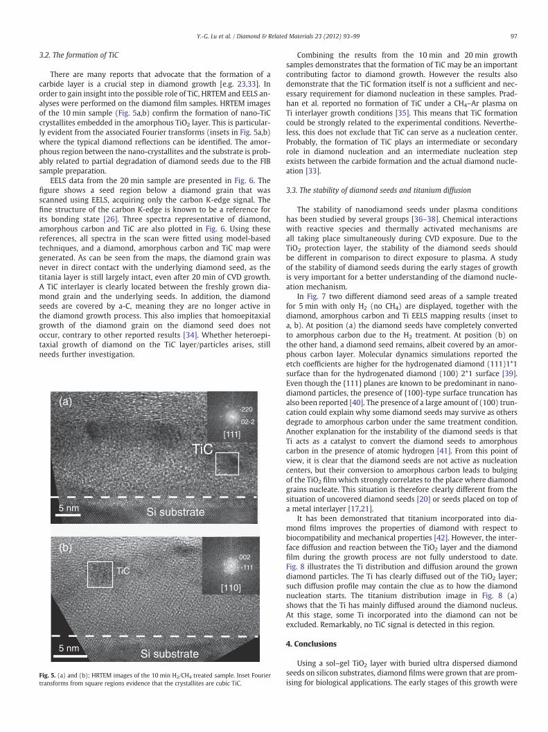
3.2. The formation of TiC
There are many reports that advocate that the formation of acarbide layer is a crucial step in diamond growth [e.g. 23,33]. Inorder to gain insight into the possible role of TiC, HRTEM and EELS an-alyses were performed on the diamond film samples. HRTEM imagesof the 10 min sample (Fig. 5a,b) confirm the formation of nano-TiCcrystallites embedded in the amorphous TiO2 layer. This is particular-ly evident from the associated Fourier transforms (insets in Fig. 5a,b)where the typical diamond reflections can be identified. The amor-phous region between the nano-crystallites and the substrate is prob-ably related to partial degradation of diamond seeds due to the FIBsample preparation.
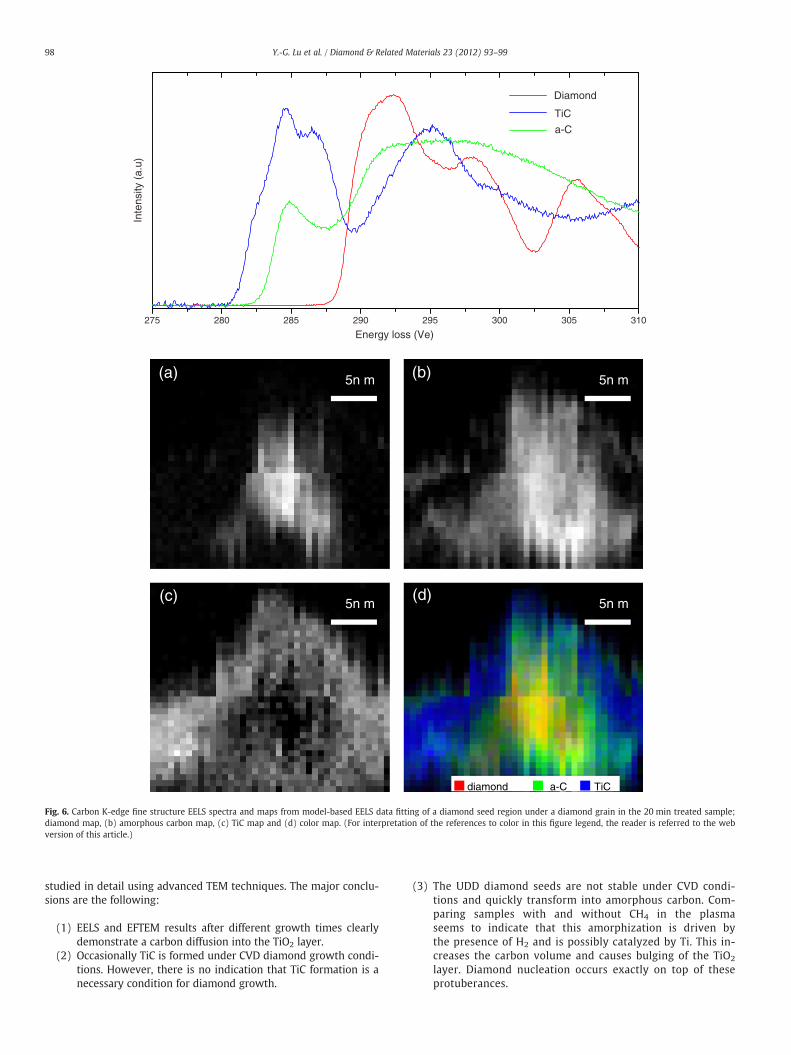
EELS data from the 20 min sample are presented in Fig. 6. Thefigure shows a seed region below a diamond grain that wasscanned using EELS, acquiring only the carbon K-edge signal. Thefine structure of the carbon K-edge is known to be a reference forits bonding state [26]. Three spectra representative of diamond,amorphous carbon and TiC are also plotted in Fig. 6. Using thesereferences, all spectra in the scan were fitted using model-basedtechniques, and a diamond, amorphous carbon and TiC map weregenerated. As can be seen from the maps, the diamond grain wasnever in direct contact with the underlying diamond seed, as thetitania layer is still largely intact, even after 20 min of CVD growth.A TiC interlayer is clearly located between the freshly grown dia-mond grain and the underlying seeds. In addition, the diamondseeds are covered by a-C, meaning they are no longer active inthe diamond growth process. This also implies that homoepitaxialgrowth of the diamond grain on the diamond seed does notoccur, contrary to other reported results [34]. Whether heteroepi-taxial growth of diamond on the TiC layer/particles arises, stillneeds further investigation.
5 nm Si substrate
(a)
TiC
TiC
5 nm Si substrate
[110]
(b)
[111]
-220
02-2
002
-111
Fig. 5. (a) and (b); HRTEM images of the 10 min H2/CH4 treated sample. Inset Fouriertransforms from square regions evidence that the crystallites are cubic TiC.
Combining the results from the 10 min and 20 min growthsamples demonstrates that the formation of TiC may be an importantcontributing factor to diamond growth. However the results alsodemonstrate that the TiC formation itself is not a sufficient and nec-essary requirement for diamond nucleation in these samples. Prad-han et al. reported no formation of TiC under a CH4–Ar plasma onTi interlayer growth conditions [35]. This means that TiC formationcould be strongly related to the experimental conditions. Neverthe-less, this does not exclude that TiC can serve as a nucleation center.Probably, the formation of TiC plays an intermediate or secondaryrole in diamond nucleation and an intermediate nucleation stepexists between the carbide formation and the actual diamond nucle-ation [33].
3.3. The stability of diamond seeds and titanium diffusion
The stability of nanodiamond seeds under plasma conditionshas been studied by several groups [36–38]. Chemical interactionswith reactive species and thermally activated mechanisms areall taking place simultaneously during CVD exposure. Due to theTiO2 protection layer, the stability of the diamond seeds shouldbe different in comparison to direct exposure to plasma. A studyof the stability of diamond seeds during the early stages of growthis very important for a better understanding of the diamond nucle-ation mechanism.
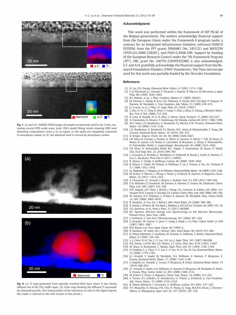
In Fig. 7 two different diamond seed areas of a sample treatedfor 5 min with only H2 (no CH4) are displayed, together with thediamond, amorphous carbon and Ti EELS mapping results (inset toa, b). At position (a) the diamond seeds have completely convertedto amorphous carbon due to the H2 treatment. At position (b) onthe other hand, a diamond seed remains, albeit covered by an amor-phous carbon layer. Molecular dynamics simulations reported theetch coefficients are higher for the hydrogenated diamond (111)1*1surface than for the hydrogenated diamond (100) 2*1 surface [39].Even though the {111} planes are known to be predominant in nano-diamond particles, the presence of {100}-type surface truncation hasalso been reported [40]. The presence of a large amount of (100) trun-cation could explain why some diamond seeds may survive as othersdegrade to amorphous carbon under the same treatment condition.Another explanation for the instability of the diamond seeds is thatTi acts as a catalyst to convert the diamond seeds to amorphouscarbon in the presence of atomic hydrogen [41]. From this point ofview, it is clear that the diamond seeds are not active as nucleationcenters, but their conversion to amorphous carbon leads to bulgingof the TiO2 film which strongly correlates to the place where diamondgrains nucleate. This situation is therefore clearly different from thesituation of uncovered diamond seeds [20] or seeds placed on top ofa metal interlayer [17,21].
It has been demonstrated that titanium incorporated into dia-mond films improves the properties of diamond with respect tobiocompatibility and mechanical properties [42]. However, the inter-face diffusion and reaction between the TiO2 layer and the diamondfilm during the growth process are not fully understood to date.Fig. 8 illustrates the Ti distribution and diffusion around the growndiamond particles. The Ti has clearly diffused out of the TiO2 layer;such diffusion profile may contain the clue as to how the diamondnucleation starts. The titanium distribution image in Fig. 8 (a)shows that the Ti has mainly diffused around the diamond nucleus.At this stage, some Ti incorporated into the diamond can not beexcluded. Remarkably, no TiC signal is detected in this region.
4. Conclusions
Using a sol–gel TiO2 layer with buried ultra dispersed diamondseeds on silicon substrates, diamond films were grown that are prom-ising for biological applications. The early stages of this growth were
diamond a-C TiC
(a)
(d)(c)
(b)
Energy loss (Ve)
Inte
nsity
(a.
u)
Diamond
TiC
a-C
275 300295290285280 305 310
5n m
5n m 5n m
5n m
Fig. 6. Carbon K-edge fine structure EELS spectra and maps from model-based EELS data fitting of a diamond seed region under a diamond grain in the 20 min treated sample;diamond map, (b) amorphous carbon map, (c) TiC map and (d) color map. (For interpretation of the references to color in this figure legend, the reader is referred to the webversion of this article.)
98 Y.-G. Lu et al. / Diamond & Related Materials 23 (2012) 93–99
studied in detail using advanced TEM techniques. The major conclu-sions are the following:
(1) EELS and EFTEM results after different growth times clearlydemonstrate a carbon diffusion into the TiO2 layer.
(2) Occasionally TiC is formed under CVD diamond growth condi-tions. However, there is no indication that TiC formation is anecessary condition for diamond growth.
(3) The UDD diamond seeds are not stable under CVD condi-tions and quickly transform into amorphous carbon. Com-paring samples with and without CH4 in the plasmaseems to indicate that this amorphization is driven bythe presence of H2 and is possibly catalyzed by Ti. This in-creases the carbon volume and causes bulging of the TiO2
layer. Diamond nucleation occurs exactly on top of theseprotuberances.
20 nmdiamond a-C Ti
20 nma-C Ti
(a)
(b)
Fig. 7. (a) and (b); HAADF-STEM images of samples treated only with H2 for 5 min, con-taining several UDD seeds areas. Inset; EELS model fitting results showing UDD seedelemental compositions (inset a, b). In region (a) the seeds are completely convertedto amorphous carbon, in (b) the diamond seed is covered by amorphous carbon.
(a)
(b)
diamond Ti
20 nm
20 nm
Fig. 8. (a) Ti map generated from spatially resolved EELS data. Some Ti has clearlydiffused out of the TiO2 buffer layer. (b) Color map showing the diffused Ti surroundsthe diamond growth. (For interpretation of the references to color in this figure legend,the reader is referred to the web version of this article.)
99Y.-G. Lu et al. / Diamond & Related Materials 23 (2012) 93–99
Acknowledgment
This work was performed within the framework of IAP P6/42 ofthe Belgian government. The authors acknowledge financial supportfrom the European Union under the Framework 6 program under acontract for an Integrated Infrastructure Initiative, reference 026019ESTEEM, from the FP7 grants DINAMO (No. 245122) and MATCON(PITN-GA-2009-238201), and FWO-G.0568.10N. Support by fundingof the European Research Council under the 7th Framework Program(FP7), ERC grant No. 246791-COUNTATOMS is also acknowledged.S.T. and A.H. gratefully acknowledge the financial support from the Re-search Foundation-Flanders (FWO-Vlaanderen). The Titanmicroscopeused for this work was partially funded by the Hercules Foundation.
References
[1] H. Liu, D.S. Dandy, Diamond Relat. Mater. 4 (1995) 1173–1188.[2] F. Le Normand, J.C. Arnault, V. Parasote, L. Fayette, B. Marcus, M. Mermoux, J. Appl.
Phys. 80 (1996) 1830–1845.[3] R.S. Balmer, et al., J. Phys. Condens. Matter 21 (2009) 364221.[4] M. Daenen, L. Zhang, R. Erni, O.A. Williams, A. Hardy, M.K. Van Bael, P. Wagner, K.
Haenen, M. Nesládek, G. Van Tendeloo, Adv. Mater. 21 (2009) 670–673.[5] J.J. Gracio, et al., J. Phys. D: Appl. Phys. 43 (2010) 374017.[6] L. Zhu, X. Ye, G. Tang, N. Zhao, Y. Gong, Y. Zhao, J. Zhao, X. Zhang, J. Biomed. Mater.
Res. Part A 78A (2006) 515–522.[7] R. Lima, B. Marple, H. Li, K. Khor, J. Therm. Spray Technol. 15 (2006) 623–627.[8] O. Yamamoto, K. Alvarez, Y. Kashiwaya, M. Fukuda, Carbon 49 (2011) 1588–1598.[9] M.S. Amin, L.K. Randeniya, A. Bendavid, P.J. Martin, E.W. Preston, Diamond Relat.
Mater. 18 (2009) 1139–1144.[10] L.K. Randeniya, A. Bendavid, P.J. Martin, M.S. Amin, R. Rohanizadeh, F. Tang, J.M.
Cairney, Diamond Relat. Mater. 19 (2010) 329–335.[11] A. Krüger, Angew. Chem. Int. Ed. 45 (2006) 6426–6427.[12] F.R. Kloss, R. Gassner, J. Preiner, A. Ebner, K. Larsson, O. Hächl, T. Tuli, M. Rasse, D.
Moser, K. Laimer, E.A. Nickel, G. Laschober, R. Brunauer, G. Klima, P. Hinterdorfer,D. Steinmüller-Nethl, G. Lepperdinger, Biomaterials 29 (2008) 2433–2442.
[13] F.R. Kloss, D. Steinmüller-Nethl, R.G. Stigler, T. Ennemoser, M. Rasse, O. Hächl,Clin. Oral Impl. Res. 22 (2010) 699–705.
[14] L. Grausova, A. Kromka, Z. Burdikova, A. Eckhardt, B. Rezek, J. Vacik, K. Haenen, V.Lisa, L. Bacakova, PLoS One 6 (2011) e20943.
[15] R. Shima, Y. Chakk, A. Hoffman, Carbon 38 (2000) 1839–1843.[16] R. Shima, Y. Chakk, M. Folman, A. Hoffman, F. Lai, S. Prawer, J. Vac. Sci. Technol. B
17 (1999) 1912–1918.[17] J.G. Buijnsters, L. Vázquez, J.J. terMeulen, Diamond Relat. Mater. 18 (2009) 1239–1246.[18] M. Eckert, V. Mortet, L. Zhang, E. Neyts, J. Verbeeck, K. Haenen, A. Bogaerts, Chem.
Mater. 23 (2011) 1414–1423.[19] A. Chavanne, J.C. Arnault, J. Barjon, J. Arabski, Surf. Sci. 605 (2011) 564–569.[20] O.A. Williams, O. Douhéret, M. Daenen, K. Haenen, E. Osawa, M. Takahashi, Chem.
Phys. Lett. 445 (2007) 255–258.[21] N.N. Naguib, J.W. Elam, J. Birrell, J. Wang, D.S. Grierson, B. Kabius, J.M. Hiller, A.V.
Sumant, R.W. Carpick, O. Auciello, J.A. Carlisle, Chem. Phys. Lett. 430 (2006) 345–350.[22] M. Daenen, O.A. Williams, J. D'Haen, K. Haenen, M. Nesládek, Phys. Status Solidi
(a) 203 (2006) 3005–3010.[23] R. Haubner, B. Lux, Int. J. Refract. Met. Hard Mater 24 (2006) 380–386.[24] A. Hardy, J. D'Haen, M. Van Bael, J. Mullens, J. Sol-Gel Sci. Technol. 44 (2007) 65–74.[25] S.D. Janssens, et al., New J. Phys. 13 (2011) 083008.[26] R.F. Egerton, Electron Energy Loss Spectroscopy in the Electron Microscope,
Plenum Press, New York, 1996.[27] J. Verbeeck, S. Van Aert, Ultramicroscopy 101 (2004) 207–224.[28] A. Krueger, M. Ozawa, G. Jarre, Y. Liang, J. Stegk, L. Lu, Phys. Status Solidi (a) 204
(2007) 2881–2887.[29] R.H. Benno Lux, Pure Appl. Chem. 66 (1994) 6.[30] R. Haubner, W. Kalss, Int. J. Refract. Met. Hard Mater 28 (2010) 475–483.[31] R. Shima Edelstein, I. Gouzman, M. Folman, A. Hoffman, S. Rotter, Diamond Relat.
Mater. 8 (1999) 139–145.[32] L.-J. Chen, N.-H. Tai, C.-Y. Lee, I.N. Lin, J. Appl. Phys. 101 (2007) 064308.[33] B.R. Stoner, G.H.M. Ma, S.D. Wolter, J.T. Glass, Phys. Rev. B 45 (1992) 11067.[34] M. Ihara, H. Komiyama, T. Okubo, Appl. Phys. Lett. 65 (1994) 1192–1194.[35] D. Pradhan, L.-J. Chen, Y.-C. Lee, C.-Y. Lee, N.-H. Tai, I.N. Lin, Diamond Relat. Mater.
15 (2006) 1779–1783.[36] J.C. Arnault, S. Saada, M. Nesladek, O.A. Williams, K. Haenen, P. Bergonzo, E.
Osawa, Diamond Relat. Mater. 17 (2008) 1143–1149.[37] S. Zeppilli, J.C. Arnault, C. Gesset, P. Bergonzo, R. Polini, Diamond Relat. Mater. 19
(2010) 846–853.[38] J.C. Arnault, S. Saada, O.A. Williams, K. Haenen, P. Bergonzo, M. Nesladek, R. Polini,
E. Osawa, Phys. Status Solidi (a) 205 (2008) 2108–2113.[39] M. Eckert, E. Neyts, A. Bogaerts, Chem. Vap. Depos. 14 (2008) 213–223.[40] S. Turner, O.I. Lebedev, O. Shenderova, I.I. Vlasov, J. Verbeeck, G. Van Tendeloo,
Adv. Funct. Mater. 19 (2009) 2116–2124.[41] R. Shima-Edelstein, I. Gouzman, A. Hoffman, Carbon 39 (2001) 337–342.[42] P.V. Bharathy, D. Nataraj, P.K. Chu, H. Wang, Q. Yang, M.S.R.N. Kiran, J. Silvestre-
Albero, D. Mangalaraj, Appl. Surf. Sci. 257 (2010) 143–150.
Related Documents


![PERFORMANCE ENHANCEMENT OF DYE …with CNT. In order to optimize the structure of photoelectrode in DSSCs, three different layers of TiO2 were designed by Hu et al. [9]. These layers](https://static.cupdf.com/doc/110x72/5f7f6d91a2a1ff164601ac1d/performance-enhancement-of-dye-with-cnt-in-order-to-optimize-the-structure-of-photoelectrode.jpg)


