Analog Integrated Circuits Lecture 6: Noise Analysis Analog Integrated Circuits Lecture 6: Noise Analysis ELC 601 – Fall 2013 Dr. Ahmed Nader Dr. Mohamed M. Aboudina [email protected] [email protected] Department of Electronics and Communications Engineering Faculty of Engineering – Cairo University

Welcome message from author
This document is posted to help you gain knowledge. Please leave a comment to let me know what you think about it! Share it to your friends and learn new things together.
Transcript
Analog Integrated Circuits
Lecture 6: Noise Analysis
Analog Integrated Circuits
Lecture 6: Noise Analysis
ELC 601 – Fall 2013
Dr. Ahmed Nader
Dr. Mohamed M. Aboudina
Department of Electronics and Communications Engineering
Faculty of Engineering – Cairo University

• The phenomenon of noise and its effect on analog circuits.
• Noise characteristics in the frequency and time domains.
– Thermal noise
– Shot noise (in BJT)
– Flicker noise
• Methods of representing noise in circuits.
• Noise in single-stage and differential amplifiers.
Noise Overview

� Noise is a random process, which means the
value of noise cannot be predicted at any
time.
� How can we incorporate noise in circuit
analysis? This is accomplished by observing
the noise for a long time and using the
measured results to construct a “statistical
model” for the noise. While the
instantaneous amplitude of noise cannot be
predicted, a statistical model provides
knowledge about some other important
properties of the noise that prove useful and
adequate in circuit analysis.
Statistical Characteristics of Noise

High-power random signalLow-power random signal
Since the signal are not periodic, the measurement must be carried out over a
long time:
( )
∫+
−∞→=
2/
2/
21lim
T
TL
Tav dt
R
tx
TP
where x(t) is a voltage quantity.
Average Power of Random Signals

To simplify calculations, we write the definition of Pav as
( )∫+
−∞→=
2/
2/
21lim
T
TTav dttx
TP
where Pav is expressed in V2 rather than W.
In analogy with deterministic signals, we can also define a root-mean-square
(rms) voltage for noise as avP .
Average Noise Power

• Calculation of noise spectrum
� Power spectral density (PSD):
The spectrum shows how much power the signal
carries at each frequency. More specifically, the
PSD, SX(f), of a noise waveform x(t) is defined as
the average power carried by x(t) in a one-hertz
bandwidth around f. SX(f) is expresses in V2/Hz.
� We can apply x(t) to a bandpass filter with center
frequency f1 and 1-Hz bandwidth, square the output,
and calculate the average over a long time to obtain
SX(f1). Repeating the procedure for different center
frequencies, we arrive at the overall shape of SX(f).
� It is also common to take the square root of SX(f),
expressing the result in HzV / .
� In summary, the spectrum shows the power
carried in a small bandwidth at each frequency,
revealing how fast the waveform is expected
to vary in the time domain.
Noise Spectrum

• White spectrum (white noise)
• Noise shaping by a transfer function
• Example: Spectral shaping by telephone BW
( ) ( ) ( ) 2fHfSfS XY =
Noise Shaping

• Two-sided and one-sided noise spectra
• Folded white spectrum
Since SX(f) is an even function of f for real x(t), the total power carried by
x(t) in the frequency range [f1 f2] is equal to
( ) ( ) ( )∫∫∫+
+
+
+
−
−=+= 2
1
2
1
1
221
2,
f
f X
f
f X
f
f Xff dffSdffSdffSP
Spectrum Power

• Probability density function (PDF)� Probability density function (PDF): By observing the noise waveform for a long
time, we can construct a “distribution” of the amplitude, indicating how often each
value occurs. The distribution of x(t) is defined as
pdf(x)dx = probability of x < X < x +dx,
where X is the measured value of x(t) at some point in time.
� Gaussian PDF is defined as ( )
2
2
2exp
2
1)(
σπσmx
xpdf−−
= ,
where σ and m are the standard deviation and mean of the distribution,
respectively.
Amplitude Distribution

Uncorrelated noise Correlated noise
We add two noise waveforms and take average of the resulting power:
( ) ( )[ ]
( ) ( ) ( ) ( )
( ) ( )∫
∫∫∫
∫
+
−∞→
+
−∞→
+
−∞→
+
−∞→
+
−∞→
++=
++=
+=
2/T
2/T21
T2av1av
2/T
2/T21
T
2/T
2/T
2
2T
2/T
2/T
2
1T
2/T
2/T
2
21T
av
dttxtx2T
1limPP
dttxtx2T
1limdttx
T
1limdttx
T
1lim
dttxtxT
1limP
correlation
Correlated and Uncorrelated Sources

• Thermal noise of a resistor
The thermal noise of a resistor R can be modeled by a series voltage source, with the
one-sided spectral density
2nV = Sv(f) = 4kTR, f ≥ 0,
where k = 1.38×10⁻²³
J/K is the Boltzmann constant and Sv(f) is expressed in V2/Hz.
Resistor Thermal Noise (1/3)

• Example: low-pass filter
We compute the transfer function from VR to Vout: ( )1
1
+=
RCss
V
V
R
out
From the theorem, we have ( ) ( ) ( )14
14
2222
2
+==
fCRkTRf
V
VfSfS
R
outRout π
.
The total noise power at the output:
C
kT
u
uu
C
kTdf
fCR
kTRP outn =
=
∞==
+= −∞
∫0
tan2
14
4 1
0 2222, ππ (V
2)
Resistor Thermal Noise (2/3)

• Representation of resistor thermal noise by a current
source
• Example
R
kT
R
VI n
n
42
22 == (A
2/Hz)
� Since the two noise sources are uncorrelated, we add the powers:
+=+=
21
22
21
2,
114
RRkTIII nntotn
� The equivalent noise voltage is given by
( ) ( )21
2
212,
2, 4 RRkTRRIV totntotn ==
Resistor Thermal Noise (3/3)
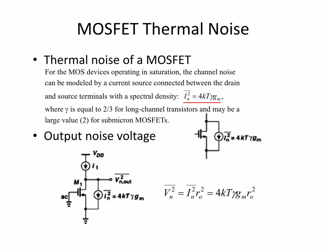
MOSFET Thermal Noise
• Thermal noise of a MOSFET
• Output noise voltage
For the MOS devices operating in saturation, the channel noise
can be modeled by a current source connected between the drain
and source terminals with a spectral density: mn gkTI γ42 = ,
where γ is equal to 2/3 for long-channel transistors and may be a
large value (2) for submicron MOSFETs.
2222 4 omonn rgkTrIV γ==

• Dangling bonds at the oxide-silicon interface
� As charge carriers move at the interface, some are
randomly trapped and later released by such energy
states, introducing flicker noise in the drain current.
� The flicker noise is modeled as a voltage source in
series with the gate and roughly given by
fWLC
KV
ox
n
12 ⋅= , where K is a process-dependent
constant on the order of 10−25
V2F.
� The flicker noise is also called 1/f noise, and it does
not depend on the bias current or the temperature.
� It is believed that PMOS devices exhibit less 1/f
noise than NMOS transistors because the former
carry the holes in a “buried channel”, i.e., at some
distance from the oxide-silicon interface.
Flicker Noise (1/2)
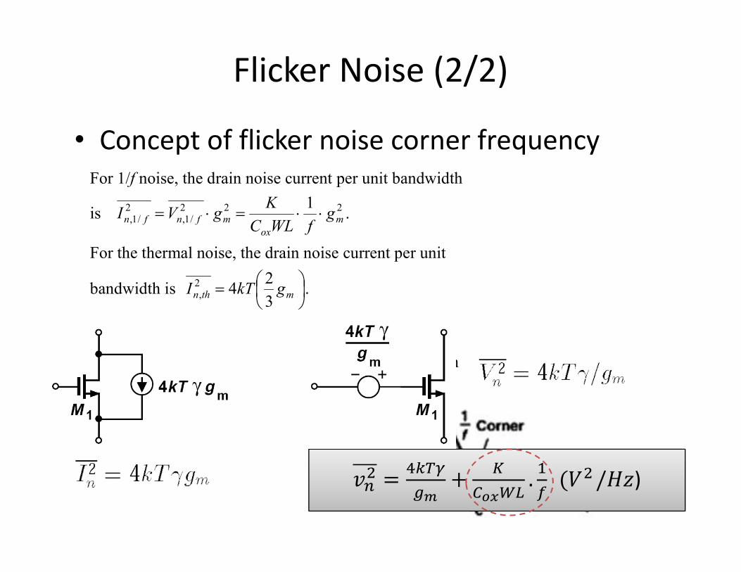
• Concept of flicker noise corner frequency
For 1/f noise, the drain noise current per unit bandwidth
is 222
/1,2
/1,
1m
ox
mfnfn gfWLC
KgVI ⋅⋅=⋅= .
For the thermal noise, the drain noise current per unit
bandwidth is
= mthn gkTI
3
242
, .
Thus, the 1/f noise corner, fC, of the output current is
determined by kT
gWLC
Kf m
ox
C8
3= , which depends on
device dimensions and bias current.
Flicker Noise (2/2)
��� �
����
�
�
����.�
����/����
� �����
�
�
����.�
����/��)

MOS Noise
��� �
����
�
�
����.�
����/����
� �����
�
�
����.�
����/��)

Lemma
Assignment 4a:Prove this Lemma
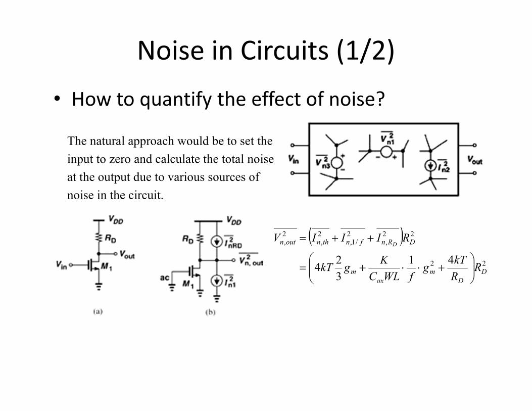
• How to quantify the effect of noise?
• Example
The natural approach would be to set the
input to zero and calculate the total noise
at the output due to various sources of
noise in the circuit.
( )22
22,
2/1,
2,
2,
41
3
24 D
D
m
ox
m
DRnfnthnoutn
RR
kTg
fWLC
KgkT
RIIIVD
+⋅⋅+=
++=
Noise in Circuits (1/2)

• Determination of input-referred noise voltage
� If the voltage gain is Av, then we have 2,
22, innvoutn VAV = , that is, the input-referred
noise voltage is given by the output noise voltage divided by the gain.
� The input-referred noise indicates how much the input signal is corrupted by the
circuit’s noise, i.e., how small an input the circuit can detect with acceptable SNR.
� The input-referred noise is a fictitious quantity in that it cannot be measured at the
input of the circuit.
Noise in Circuits (2/2)

• CS stage
• Discussion
222,
41
3
24 D
D
m
ox
moutn RR
kTg
fWLC
KgkTV
+⋅⋅+=
fWLC
K
RggkT
A
VV
oxDmmv
outn
inn
11
3
24
22
2,2
, +
+==
Voltage Amplification Current Generation
� How can we reduce the input-referred noise
voltage? It implies that the transconductance
of M1 must be maximized.
� The transconductance must be maximized if
the transistor is to amplify a voltage signal
applied to its gate [Fig.(a)] whereas it must
be minimized if the transistor operates as a
current source [Fig.(b)].
Common-Source Stage (1/3)

• Example: calculate the input-referred thermal noise voltage of the amplifier
Thermal noise: ( )221212,
3
2
3
24 oommoutn rrggkTV
+=
Voltage gain: |Av| = gm1(ro1||ro2)
The total noise voltage referred to the gate of M1 is
+=
+=
21
2
12
1
212,
3
2
3
24
1
3
2
3
24
m
m
mm
mminng
g
gkT
gggkTV
It reveals the dependence of 2,innV upon gm1 and gm2, confirming that gm2
must be minimized because M2 serves as a current source.
Common-Source Stage (2/3)

• How to design a CS stage for low-noise
operation?
� For thermal noise, we must maximize gm by increasing the drain current or the device
width. A higher ID translates to greater power dissipation and limited output voltage
swings while a wider device leads to larger input and output capacitance. We can also
increase RD, but at the cost of limiting the voltage headroom and lowering the speed.
� For 1/f noise, the primary approach is to increase the area of the transistor. If WL is
increased while W/L remains constant, then the device gm and its thermal noise do not
change but the device capacitances increase.
� These observations point to the trade-offs between noise, power dissipation,
voltage headroom, and speed.
fWLC
K
RggkT
A
VV
oxDmmv
outn
inn
11
3
24
22
2,2
, +
+==
Common-Source Stage (3/3)

� Since the input impedance of the source follower is quite
high, the input-referred noise current can usually be
neglected for moderate driving source impedance.
� Compute the input-referred thermal noise:
2
21
11
22
2,
112
= oo
mbm
nMoutn rrgg
IV (thermal noise)
and
1
21
1
21
1
11
1
m
oo
mb
oo
mbv
grr
g
rrg
A
+
=
then
+=+=
21
2
12
2,2
12,
1
3
242
m
m
mv
Moutn
ninng
g
gkT
A
VVV
Source Followers (1/2)

� Compute the input-referred 1/f noise:
( )( )
( )( )22
2
2
1
1
2,
11outm
ox
outm
ox
outn RgfWLC
KRg
fWLC
KV +=
and outmvoo
mbm
out RgArrgg
R 121
11
,11
=
=
then ( ) ( )
+==
21
22
2
2,2
,
1
m
m
oxv
outn
inngWL
g
WLfC
K
A
VV
Source Followers (2/2)

• Representation of input-referred noise by voltage and current sources
• Calculation of input-referred noise voltage (source impedance = 0)
• Calculation of input-referred noise current (source impedance = ∞)
Input-Referred Noise

Common Gate Stage (1/2)
� Since the input impedance of the source follower is quite
low, the input-referred noise current cannot be neglected
especially for high driving source impedance.

Common Gate Stage (2/2)
� Equate the output noise voltage when the
input is short circuit and divide by Av
� Equate the output noise voltage when the input
is open circuit and divide by output impednace

M1, RD: Since the noise currents of M1 and RD flow
through RD, the noise contributed by these
two devices is quantified as in a CS stage:
+=
Dmm
RMinnRgg
kTVD 2
11
,2,
1
3
24
1
M2: In Fig.(b), if the channel length modulation in M1
is neglected, then In2 + ID2 = 0, and hence M2 does
not affect Vn,out.
In Fig.(c), the voltage gain from Vn2 to the output
is quite small if the impedance at node X is large.
At high frequencies, the total capacitance at node
X, CX, gives rise to a gain:
( )sCg
R
V
V
Xm
D
n
outn
/1/1 22
,
+−
≈
increasing the output noise.
�Noise of M2 modeled by (b) a current
source and (c) a voltage source
Cascode Stage
At high frequencies, noise of cascode devices
start to show up.
Capacitor at sources of cascode devices
shorts this point to ground ���� Gain from
cascode to output increases at high
frequencies ���� Effect of noise increases.

• Differential pair circuit
• ISS contribute common-mode
noise only
• Circuit including input-referred noise source
For low-frequency operation,
the magnitude of 2,innI is
typical negligible.
Differential Pairs (1/2)
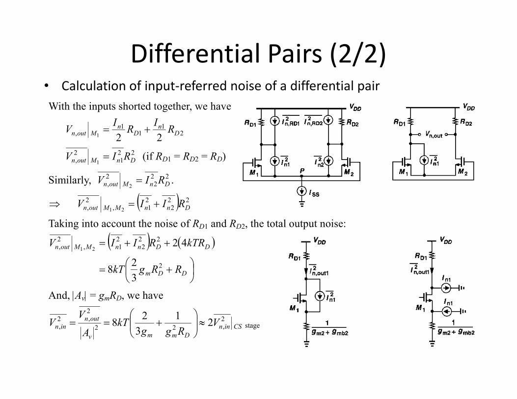
With the inputs shorted together, we have
21
11
,221 Dn
Dn
Moutn RI
RI
V +=
221
2, 1 DnMoutn RIV = (if RD1 = RD2 = RD)
Similarly, 222
2, 2 DnMoutn RIV = .
( ) 222
21,
2, 21 DnnMMoutn RIIV +=⇒
Taking into account the noise of RD1 and RD2, the total output noise:
( ) ( )
+=
++=
DDm
DDnnMMoutn
RRgkT
kTRRIIV
2
222
21,
2,
3
28
4221
And, |Av| = gmRD, we have
CSinn
Dmmv
outn
inn VRgg
kTA
VV 2
,22
2,2
, 21
3
28 ≈
+== stage
Differential Pairs (2/2)• Calculation of input-referred noise of a differential pair

• Output noise spectrum of a circuit
The total output noise:
∫∞
=0
2,
2,, dfVV outntotoutn
and ∫∞
=⋅0
2,
20 dfVBV outnn
Noise bandwidth (Bn): Bn allows a fair comparison of circuits that exhibit the same
low-frequency noise, V02, but different high-frequency transfer
functions.
Noise Bandwidth
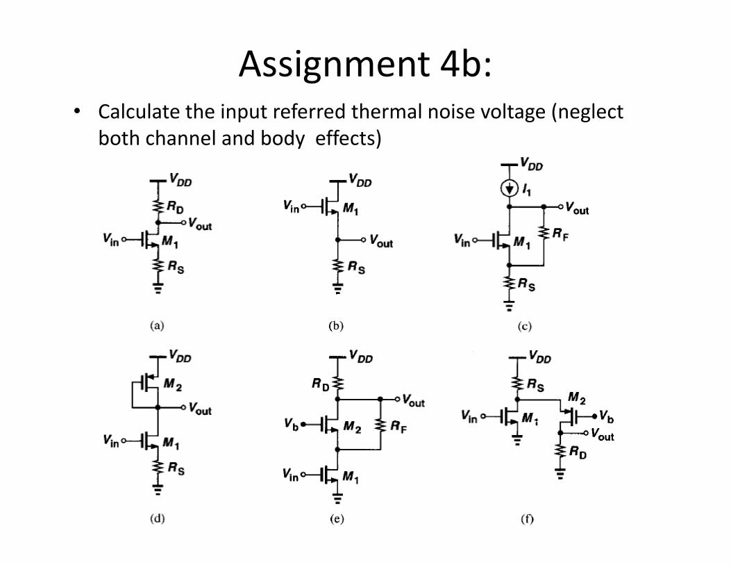
• Calculate the input referred thermal noise voltage (neglect
both channel and body effects)
Assignment 4b:
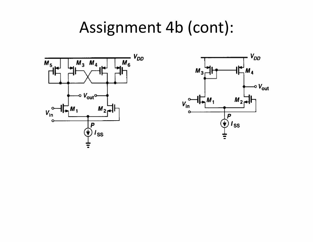
Assignment 4b (cont):
Related Documents