ATLCE - C1 19/03/2016 © 2016 DDC 1 19/03/2016 - 1 ATLCE - C1 - © 2016 DDC Analog and Telecommunication Electronics C1 - PLL linear analysis » PLL basics » Application examples » Linear analysis » Phase error AY 2015-16 Politecnico di Torino Electronic Eng. Master Degree

Welcome message from author
This document is posted to help you gain knowledge. Please leave a comment to let me know what you think about it! Share it to your friends and learn new things together.
Transcript

ATLCE - C1 19/03/2016
© 2016 DDC 1
19/03/2016 - 1 ATLCE - C1 - © 2016 DDC
Analog and Telecommunication Electronics
C1 - PLL linear analysis
» PLL basics» Application examples» Linear analysis» Phase error
AY 2015-16
Politecnico di TorinoElectronic Eng. Master Degree

ATLCE - C1 19/03/2016
© 2016 DDC 2
19/03/2016 - 2 ATLCE - C1 - © 2016 DDC
Lesson C1: PLL linear analysis
• PLL basics– How the PLL works, application examples– Block diagram of the PLL– PLL linear model
• PLL transfer function– Parameters and transfer function– Loop filter (RC, RRC, active, charge pump)– Loop gain– Phase error, transient and steady state
• References: – D. Del Corso: Elettronica per Telecomunicazioni: 3.1, 3.2– S. Franco: Design with OA and Analog IC: 13.4
ATLCE - C1 19/03/2016
© 2016 DDC 3
19/03/2016 - 3 ATLCE - C1 - © 2016 DDC
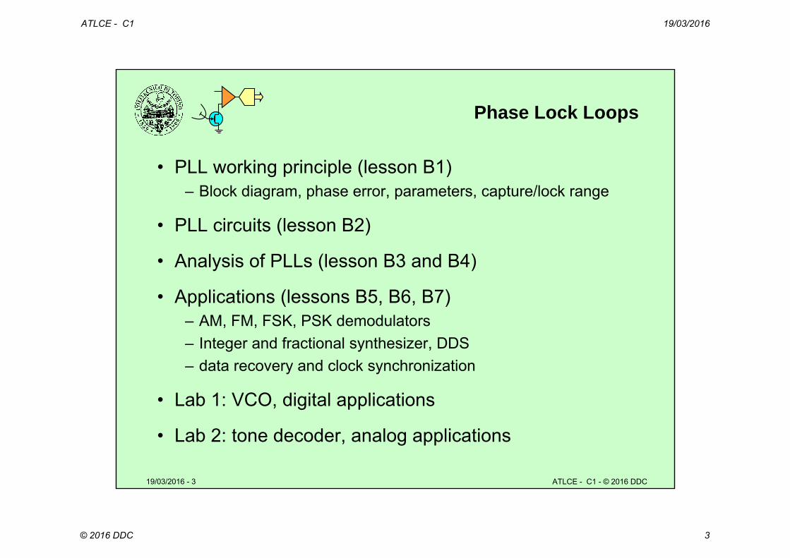
Phase Lock Loops
• PLL working principle (lesson B1)– Block diagram, phase error, parameters, capture/lock range
• PLL circuits (lesson B2)
• Analysis of PLLs (lesson B3 and B4)
• Applications (lessons B5, B6, B7)– AM, FM, FSK, PSK demodulators– Integer and fractional synthesizer, DDS– data recovery and clock synchronization
• Lab 1: VCO, digital applications
• Lab 2: tone decoder, analog applications

ATLCE - C1 19/03/2016
© 2016 DDC 4
19/03/2016 - 4 ATLCE - C1 - © 2016 DDC
PLL: where ?
• Several PLLs are used in a radio system (cell phone)
– A: local oscillator for TX frequency translation
– B: local oscillator for RX frequency translation
– C: I/Q reference signal for RX
– D: I/Q reference signals for TX
– E: clock multipliers and data synchronizer

ATLCE - C1 19/03/2016
© 2016 DDC 5
19/03/2016 - 5 ATLCE - C1 - © 2016 DDC
PLLs in the TX-RX system
Frequencysynthesizers
Generate reference signals
Synchronizersand clock multipliers.
ATLCE - C1 19/03/2016
© 2016 DDC 6
19/03/2016 - 6 ATLCE - C1 - © 2016 DDC
A real equipment
A
CB D
E

ATLCE - C1 19/03/2016
© 2016 DDC 7
19/03/2016 - 7 ATLCE - C1 - © 2016 DDC
Inside a P-RX
All local oscillator All local oscillator signals generated signals generated from a unique from a unique reference by a reference by a PLL synthesizerPLL synthesizer

ATLCE - C1 19/03/2016
© 2016 DDC 8
19/03/2016 - 8 ATLCE - C1 - © 2016 DDC
PLL applications
• Generate signals (phase) locked to a reference– AM and FM coherent demodulators– TV synchronization– Frequency synthesizers
• Resynchronization– Clock/Data recovery and separation (CDR)
• Bandpass filter with tunable parameters– Center frequency – Bandwidth and Q

ATLCE - C1 19/03/2016
© 2016 DDC 9
19/03/2016 - 9 ATLCE - C1 - © 2016 DDC
Phase synchronization examples
• Angular frequency ω is the derivative of phase θ. – Examples use sinewave/squarewave– More aesy to see phase difference θe with squarewaves
• Same frequency constant phase difference θeexample 1
• All oscillators exhibit tolerance and drift– Separate oscillators cannot provide the same frequency
example 2
• PLL: generate a signal locked to a reference– Constant θe same frequency

ATLCE - C1 19/03/2016
© 2016 DDC 10
19/03/2016 - 10 ATLCE - C1 - © 2016 DDC
Phase Lock Loop block diagram
• Vi: input signalVi(t) = Vi sin(ωit + θi)
• PD:Phase Demodulator
• F:loop filter
• VCO: Voltage Controlled Oscillator
• VO: output signal (from VCO)VO(t) = VO cos(ωot + θo)
F
PD
VI
VO VC
VD
VCO
ATLCE - C1 19/03/2016
© 2016 DDC 11
19/03/2016 - 11 ATLCE - C1 - © 2016 DDC
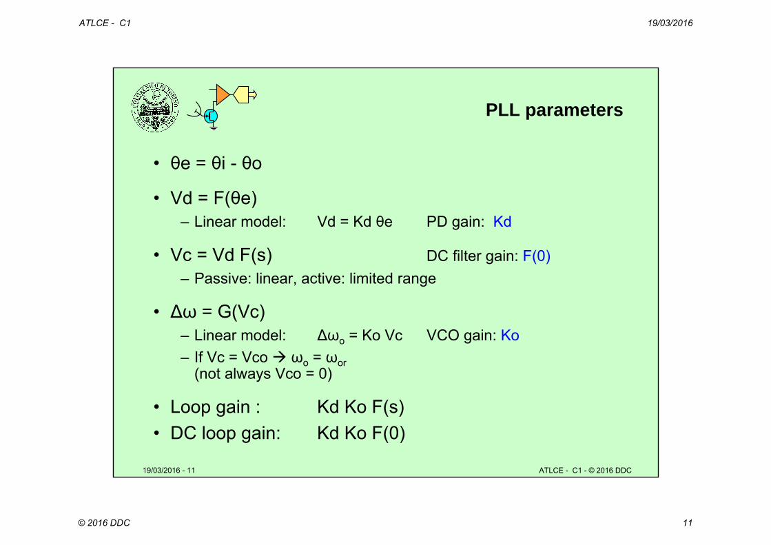
PLL parameters
• θe = θi - θo
• Vd = F(θe)– Linear model: Vd = Kd θe PD gain: Kd
• Vc = Vd F(s) DC filter gain: F(0)– Passive: linear, active: limited range
• ∆ω = G(Vc)– Linear model: ∆ωo = Ko Vc VCO gain: Ko– If Vc = Vco ωo = ωor
(not always Vco = 0)
• Loop gain : Kd Ko F(s)• DC loop gain: Kd Ko F(0)

ATLCE - C1 19/03/2016
© 2016 DDC 12
19/03/2016 - 12 ATLCE - C1 - © 2016 DDC
Linearity: where ?
• Any real circuit has a limited linearity range
• The above relations assume linearity in:
• Phase detector: Vd = Kd θe– Some PD have intrinsic nonlinear transfer function
• VCO gain: ∆ω = Ko Vc– Most VCO have nonlinear ω(Vc)
• Loop filter: F(s)– Passive; saturation if active

ATLCE - C1 19/03/2016
© 2016 DDC 13
19/03/2016 - 13 ATLCE - C1 - © 2016 DDC
Lesson B1: PLL linear analysis
• PLLs: where ?
• PLL basics– How the PLL works– Application examples– Block diagram of the PLL
• PLL transfer function– Parameters and transfer function– Loop filter– Loop gain– Phase error, transient and steady state
ATLCE - C1 19/03/2016
© 2016 DDC 14
19/03/2016 - 14 ATLCE - C1 - © 2016 DDC
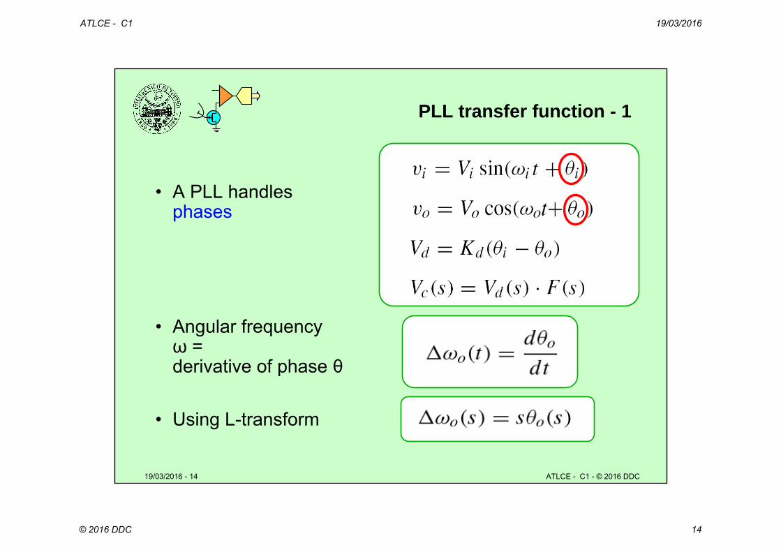
PLL transfer function - 1
• A PLL handles phases
• Angular frequencyω = derivative of phase θ
• Using L-transform

ATLCE - C1 19/03/2016
© 2016 DDC 15
19/03/2016 - 15 ATLCE - C1 - © 2016 DDC
PLL transfer function - 2
• Phase detector:
• Loop filter:
• VCO:
• Overall fdt:
ATLCE - C1 19/03/2016
© 2016 DDC 16
19/03/2016 - 16 ATLCE - C1 - © 2016 DDC
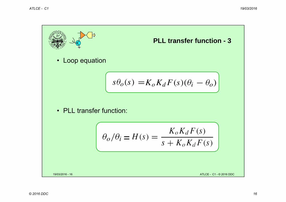
PLL transfer function - 3
• Loop equation
• PLL transfer function:
=
ATLCE - C1 19/03/2016
© 2016 DDC 17
19/03/2016 - 17 ATLCE - C1 - © 2016 DDC
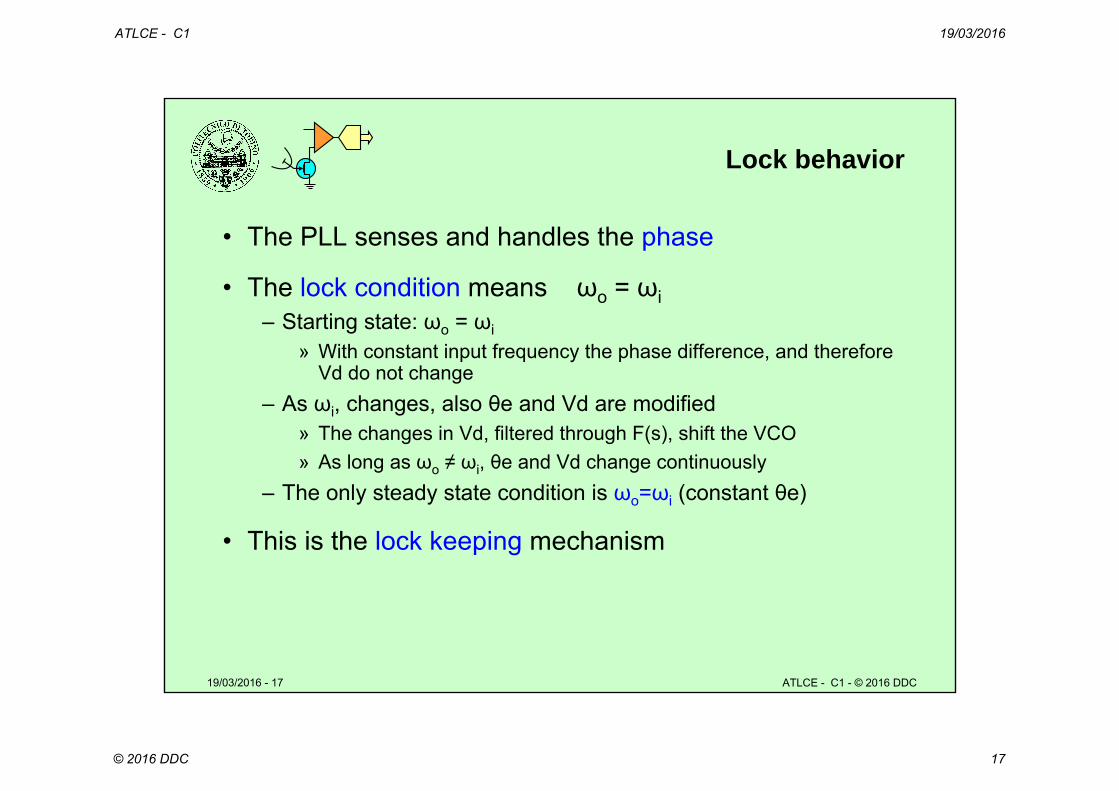
Lock behavior
• The PLL senses and handles the phase
• The lock condition means ωo = ωi– Starting state: ωo = ωi
» With constant input frequency the phase difference, and therefore Vd do not change
– As ωi, changes, also θe and Vd are modified» The changes in Vd, filtered through F(s), shift the VCO» As long as ωo ≠ ωi, θe and Vd change continuously
– The only steady state condition is ωo=ωi (constant θe)
• This is the lock keeping mechanism

ATLCE - C1 19/03/2016
© 2016 DDC 18
19/03/2016 - 18 ATLCE - C1 - © 2016 DDC
• The phase error is defined as: θe = θi - θo
• θo = θi H(s); θe= θi - θo = θi (1 - H(s))
• Same denominator as H(s)– Same parameters for time & frequency responses:
for II-order damping e resonant frequency n
Phase error
ATLCE - C1 19/03/2016
© 2016 DDC 19
19/03/2016 - 19 ATLCE - C1 - © 2016 DDC
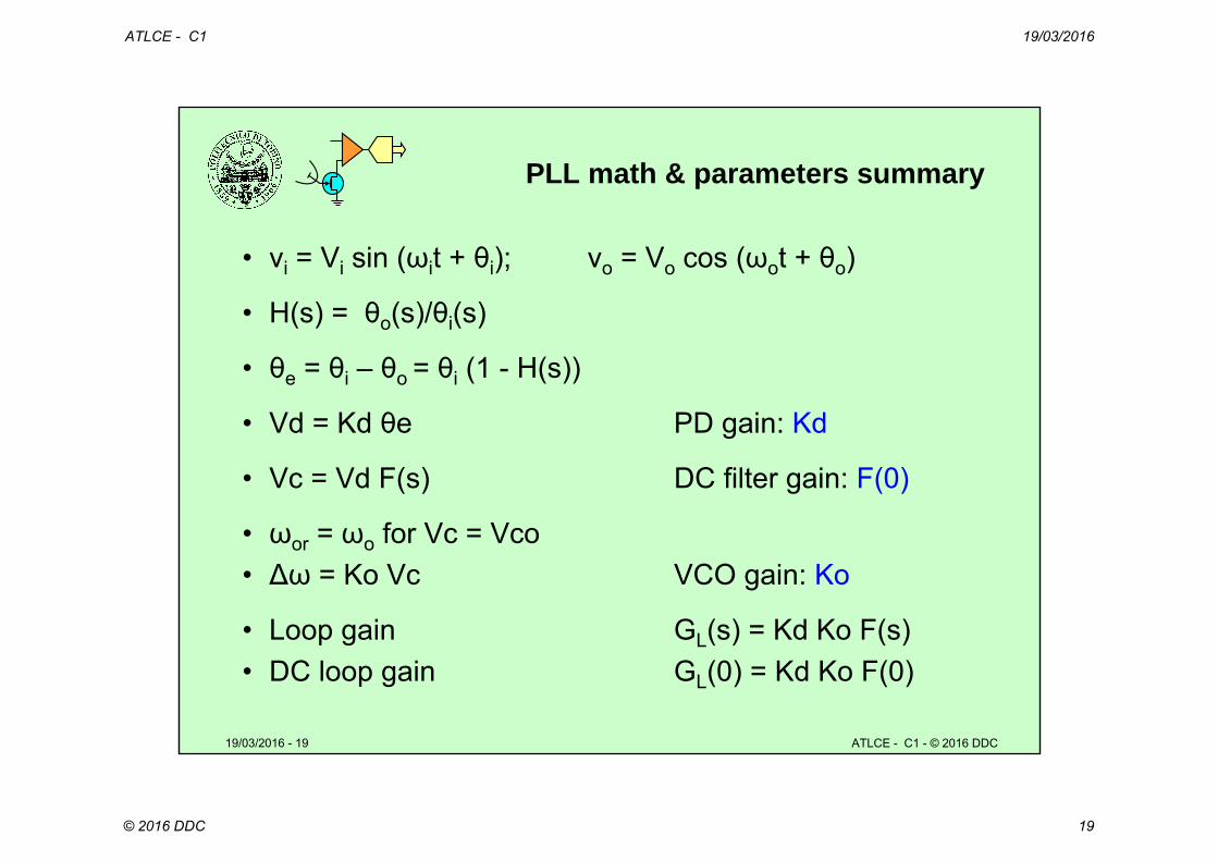
PLL math & parameters summary
• vi = Vi sin (ωit + θi); vo = Vo cos (ωot + θo)
• H(s) = θo(s)/θi(s)
• θe = θi – θo = θi (1 - H(s))
• Vd = Kd θe PD gain: Kd
• Vc = Vd F(s) DC filter gain: F(0)
• ωor = ωo for Vc = Vco• ∆ω = Ko Vc VCO gain: Ko
• Loop gain GL(s) = Kd Ko F(s)• DC loop gain GL(0) = Kd Ko F(0)
ATLCE - C1 19/03/2016
© 2016 DDC 20
19/03/2016 - 20 ATLCE - C1 - © 2016 DDC
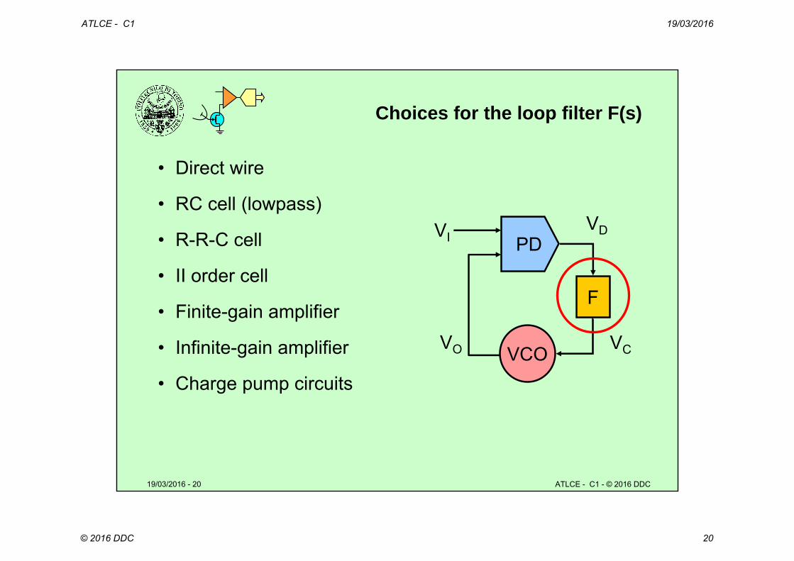
Choices for the loop filter F(s)
• Direct wire
• RC cell (lowpass)
• R-R-C cell
• II order cell
• Finite-gain amplifier
• Infinite-gain amplifier
• Charge pump circuits
F
PDVI
VO VC
VD
VCO
ATLCE - C1 19/03/2016
© 2016 DDC 21
19/03/2016 - 21 ATLCE - C1 - © 2016 DDC
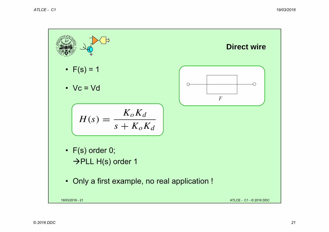
Direct wire
• F(s) = 1
• Vc = Vd
• F(s) order 0; PLL H(s) order 1
• Only a first example, no real application !

ATLCE - C1 19/03/2016
© 2016 DDC 22
19/03/2016 - 22 ATLCE - C1 - © 2016 DDC
H(s) order 1 frequency response
H(s) = 1, o = i H(s) < 1, o i
ATLCE - C1 19/03/2016
© 2016 DDC 23
19/03/2016 - 23 ATLCE - C1 - © 2016 DDC
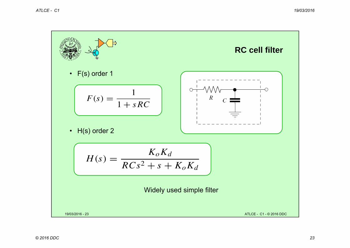
RC cell filter
• F(s) order 1
• H(s) order 2
Widely used simple filter

ATLCE - C1 19/03/2016
© 2016 DDC 24
19/03/2016 - 24 ATLCE - C1 - © 2016 DDC
H(s) in a PLL with RC filter
• Response depends on ωn , , H(0) parameters
• Three parameters
• Two degrees of freedom:Ko*Kd, R*C
• Not possible to get independent ωn , , H(0)
ATLCE - C1 19/03/2016
© 2016 DDC 25
19/03/2016 - 25 ATLCE - C1 - © 2016 DDC
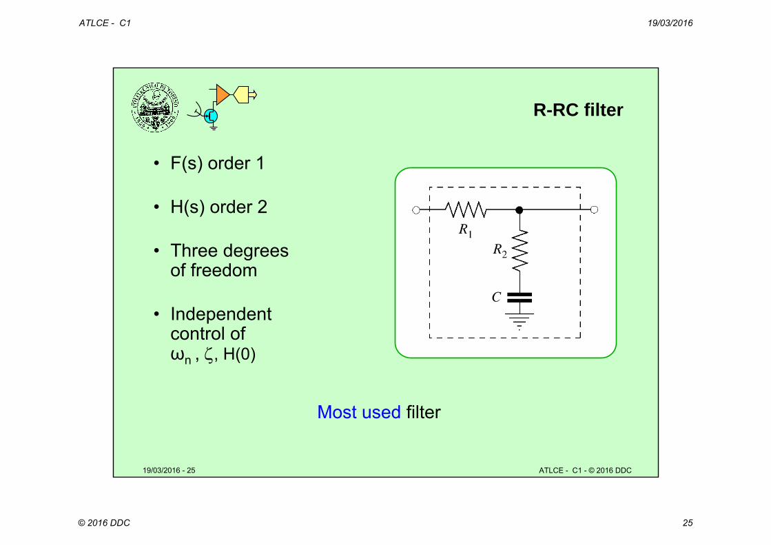
R-RC filter
• F(s) order 1
• H(s) order 2
• Three degrees of freedom
• Independent control ofωn , , H(0)
Most used filter
ATLCE - C1 19/03/2016
© 2016 DDC 26
19/03/2016 - 26 ATLCE - C1 - © 2016 DDC
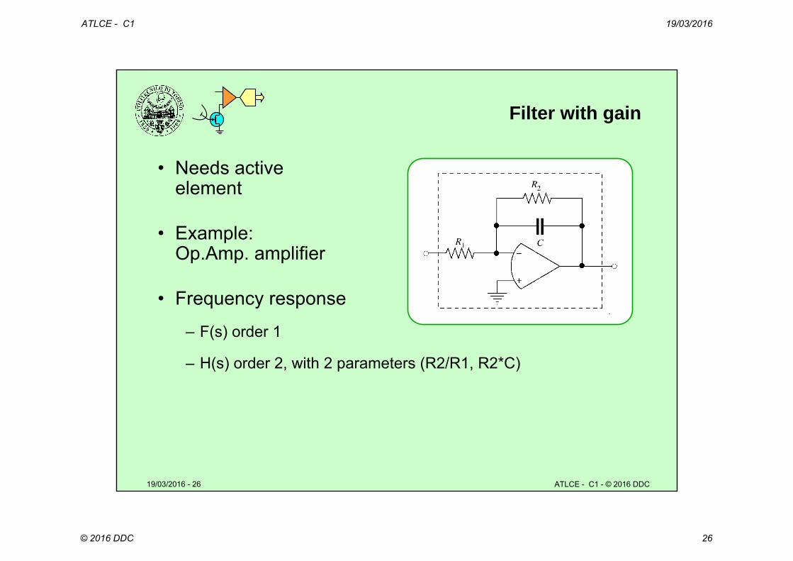
Filter with gain
• Needs active element
• Example:Op.Amp. amplifier
• Frequency response
– F(s) order 1
– H(s) order 2, with 2 parameters (R2/R1, R2*C)

ATLCE - C1 19/03/2016
© 2016 DDC 27
19/03/2016 - 27 ATLCE - C1 - © 2016 DDC
PLL order
• PLL order H(s) order
• H(s) order = F(s) order + 1
• H(s) order 1 parameter ωo
• H(s) order 2 parameters ωo and
• All cases DC gain (F(0))
ATLCE - C1 19/03/2016
© 2016 DDC 28
19/03/2016 - 28 ATLCE - C1 - © 2016 DDC
Infinite gain
• In steady state Vc = Vd F(0)
• To change ωo, Vc – and θe - must change– The ratio between phase error θe and control signal Vc
depends from Kd and F(0)
• Infinite gain (F(0) ∞), Vc 0 even for Vd = 0.– For an infinite-gain locked PLL, the phase error e = 0
• Two ways to get infinite gain
– High gain amplifier
– Charge pump

ATLCE - C1 19/03/2016
© 2016 DDC 29
19/03/2016 - 29 ATLCE - C1 - © 2016 DDC
Infinite gain with amplifier
• Active integrator, based on Op Amp– DC gain = open loop Op Amp gain

ATLCE - C1 19/03/2016
© 2016 DDC 30
19/03/2016 - 30 ATLCE - C1 - © 2016 DDC
• A closes on Vi edge, opens on Vo edge• B closes on Vo edge, opens on Vi edge
• Vc steady if– Phase error = 0
(edges occur at the same time)
• Infinite gain (equivalent!)
Charge pump circuit
Capacitor C charged or discharged through A or B
VC
A,B
Similar circuit with 3-S output and RC cell

ATLCE - C1 19/03/2016
© 2016 DDC 31
19/03/2016 - 31 ATLCE - C1 - © 2016 DDC
Infinite gain with charge pump
• Ideal integrator built with C + SW– 2 SW or 3-S output
• Similar behavior as open loop Op. Amp.– Can be seen as a “chopped” Op Amp
• No need for amplifier
• Used with CMOS circuit – needs high input impedance VCO
• Limited range (0 VDD, or bipolar)

ATLCE - C1 19/03/2016
© 2016 DDC 32
19/03/2016 - 32 ATLCE - C1 - © 2016 DDC
Lesson B1: PLL linear analysis
• PLLs: where ?
• PLL basics– How the PLL works– Application examples– Block diagram of the PLL
• PLL transfer function– Parameters and transfer function– Loop filter– Loop gain– Phase error, transient and steady state
ATLCE - C1 19/03/2016
© 2016 DDC 33
19/03/2016 - 33 ATLCE - C1 - © 2016 DDC
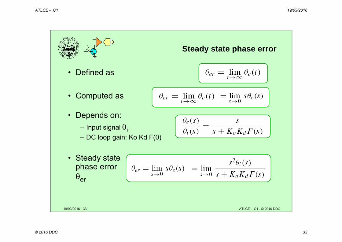
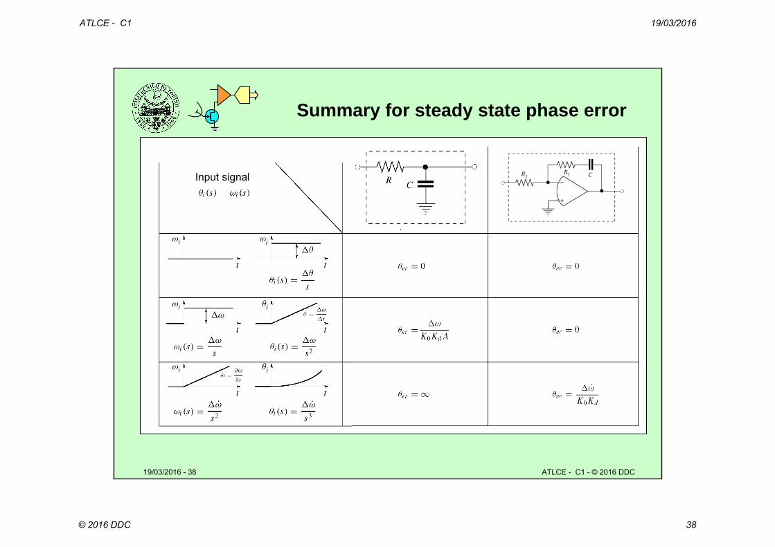
Steady state phase error
• Defined as
• Computed as
• Depends on:– Input signal i– DC loop gain: Ko Kd F(0)
• Steady state phase errorθer
ATLCE - C1 19/03/2016
© 2016 DDC 34
19/03/2016 - 34 ATLCE - C1 - © 2016 DDC
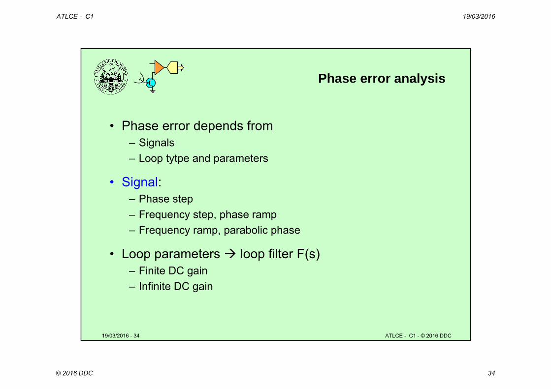
Phase error analysis
• Phase error depends from– Signals– Loop tytpe and parameters
• Signal:– Phase step– Frequency step, phase ramp– Frequency ramp, parabolic phase
• Loop parameters loop filter F(s)– Finite DC gain– Infinite DC gain
ATLCE - C1 19/03/2016
© 2016 DDC 35
19/03/2016 - 35 ATLCE - C1 - © 2016 DDC
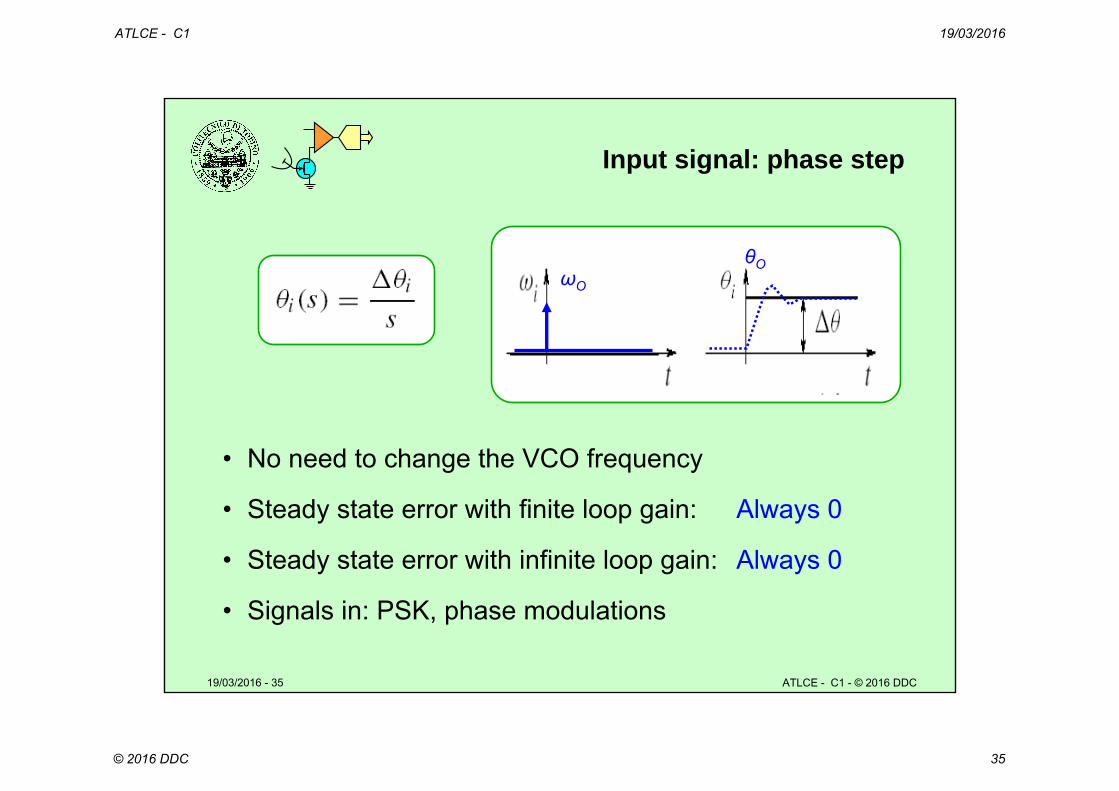
Input signal: phase step
• No need to change the VCO frequency
• Steady state error with finite loop gain: Always 0
• Steady state error with infinite loop gain: Always 0
• Signals in: PSK, phase modulations
ωO
θO

ATLCE - C1 19/03/2016
© 2016 DDC 36
19/03/2016 - 36 ATLCE - C1 - © 2016 DDC
Input signal: linear phase ramp
• The VCO frequency must be modified
• Steady state error with finite loop gain: Constant
• Steady state error with infinite loop gain: Always 0
• FSK, doppler with fixed relative speed
ωO
ATLCE - C1 19/03/2016
© 2016 DDC 37
19/03/2016 - 37 ATLCE - C1 - © 2016 DDC
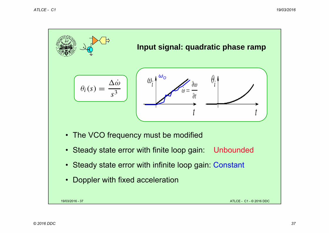
Input signal: quadratic phase ramp
• The VCO frequency must be modified
• Steady state error with finite loop gain: Unbounded
• Steady state error with infinite loop gain: Constant
• Doppler with fixed acceleration
ωO
ATLCE - C1 19/03/2016
© 2016 DDC 38
19/03/2016 - 38 ATLCE - C1 - © 2016 DDC
Summary for steady state phase error
Input signal

ATLCE - C1 19/03/2016
© 2016 DDC 39
19/03/2016 - 39 ATLCE - C1 - © 2016 DDC
Lesson B1 tests
• Mention some applications of PLLs.
• Draw the block diagram of a PLL.
• How are defined the parameters Kd, Ko, F(0) ?
• Define the PLL transfer function H(s).
• Which is the relation between F(s) and H(s)?
• List the approximations of the PLL linear model.
• How to compute the steady state phase error ?
• Evaluate θer value for linear phase ramp input to a PLL using phase detectors with finite/infinite gain Kd
Related Documents