AN11801 TEA19161 and TEA19162 controller ICs Rev. 1 — 2 June 2016 Application note Document information Info Content Keywords TEA19161, TEA19162, PFC, LLC, burst mode operation, low-power mode, cycle-by-cycle control, Vcap control, resonant power converter Abstract The TEA19161T and TEA19162T are a set of controller ICs for resonant power supplies that include a PFC. To reach a high efficiency at all power levels, the TEA19161T (LLC) introduces a new operating mode: low-power mode. This mode operates in the power region between continuous switching (now called high-power mode) and burst mode. Most LLC resonant converter controllers regulate the output power by adjusting the operating frequency. The TEA19161T regulates the output power by adjusting the voltage across the primary resonant capacitor for accurate state control and a linear power control. External presettings can define operation modes and protections. This feature provides flexibility and ease of design for optimizing controller properties to application-specific requirements.

Welcome message from author
This document is posted to help you gain knowledge. Please leave a comment to let me know what you think about it! Share it to your friends and learn new things together.
Transcript

AN11801TEA19161 and TEA19162 controller ICsRev. 1 — 2 June 2016 Application note
Document information
Info Content
Keywords TEA19161, TEA19162, PFC, LLC, burst mode operation, low-power mode, cycle-by-cycle control, Vcap control, resonant power converter
Abstract The TEA19161T and TEA19162T are a set of controller ICs for resonant power supplies that include a PFC.
To reach a high efficiency at all power levels, the TEA19161T (LLC) introduces a new operating mode: low-power mode. This mode operates in the power region between continuous switching (now called high-power mode) and burst mode.
Most LLC resonant converter controllers regulate the output power by adjusting the operating frequency. The TEA19161T regulates the output power by adjusting the voltage across the primary resonant capacitor for accurate state control and a linear power control.
External presettings can define operation modes and protections. This feature provides flexibility and ease of design for optimizing controller properties to application-specific requirements.

NXP Semiconductors AN11801TEA19161 and TEA19162 controller ICs
Revision history
Rev Date Description
v.1 <tbd> first issue
AN11801 All information provided in this document is subject to legal disclaimers. © NXP Semiconductors N.V. 2016. All rights reserved.
Application note Rev. 1 — 2 June 2016 2 of 140
Contact informationFor more information, please visit: http://www.nxp.com
For sales office addresses, please send an email to: [email protected]

NXP Semiconductors AN11801TEA19161 and TEA19162 controller ICs
1. Introduction
The TEA1916 is a fully digital controller for high-efficiency resonant power supplies. It is a 2-chip combo, which includes the TEA19161T resonant / LLC controller and the TEA19162T PFC controller. Together with the TEA1995T dual SR controller, a complete resonant power supply can be built which is easy to design and has a very low component count. This power supply meets the efficiency regulations of Energy Star, the Department of Energy (DoE), the Eco-design directive of the European Union, the European Code of Conduct, and other guidelines. So, an additional power supply for standby supply is not required.
This application note describes the TEA19161T and TEA19162T functions for different applications. It covers the functionality of the standard IC versions TEA19161T, TEA19162T, and the safe-restart versions TEA19161CT and TEA19162T. Because the combination of two controllers provides extensive functionality, a large number of topics is discussed.
This document is set up in such a way, that a chapter or paragraph of a specific topic can be read as a standalone explanation. A minimum number of cross-references to other document parts of the TEA19161T or TEA19162T data sheets is used. This document setup leads to repetition of some information within the application note and to descriptions or figures that are similar to the ones published in the data sheets. To enhance readability, only typical values are given in most cases.
The TEA19161T and TEA19162T can be considered as one PFC + HBC system controller. In this document, the one system controller is called TEA1916. Only in specific cases, the TEA19161T and TEA19162T names are used.
1.1 Related documents
For more information and tools, see the various other TEA1916 documents such as:
• Data sheets TEA19161T, TEA19161CT, TEA19162T, andTEA19162CT
• Excel calculation sheet (available on request)
• Online calculation tool
• Demo board user manuals
1.2 Related products
NXP Semiconductors products that are related to the TEA1916 ones are:
• TEA1716:
This product provides a PFC + LLC controller in an SO24 IC package. It allows low-power consumption burst mode operation.
• TEA1713:
This product provides a PFC + LLC controller in one SO24 IC package. It is more suitable for applications that do not have stringent requirements on burst mode operation.
AN11801 All information provided in this document is subject to legal disclaimers. © NXP Semiconductors N.V. 2016. All rights reserved.
Application note Rev. 1 — 2 June 2016 3 of 140

NXP Semiconductors AN11801TEA19161 and TEA19162 controller ICs
Other NXP Semiconductors products for resonant power conversion are:
• TEA1795:
Synchronous rectification controller for resonant converters with dual gate drivers in SO8.
• TEA1995:
Synchronous rectification controller for resonant converters with dual gate drivers in an SO8 package. This product is optimized for the TEA1916 operating modes.
• TEA1708:
X-capacitor discharge IC.
AN11801 All information provided in this document is subject to legal disclaimers. © NXP Semiconductors N.V. 2016. All rights reserved.
Application note Rev. 1 — 2 June 2016 4 of 140

NXP Semiconductors AN11801TEA19161 and TEA19162 controller ICs
2. TEA1916 highlights and features
2.1 Resonant conversion
The market of today demands high-quality, reliable, small, lightweight and efficient power supplies.
A resonant DC-to-DC converter produces sinusoidal currents with low switching losses. It provides the possibility of operation at higher frequencies with excellent efficiency at high power levels.
In recent years, LLC resonant converters have become more popular because of the high efficiency at medium and high output load. The latest generation of resonant controllers that support burst-mode operation have enabled good efficiency, even at low output load, a low power consumption in standby, or no-load operation.
The TEA19161 offers a next step in low-load operation. Reducing the converter power losses further and providing programmable operation behavior to make the best fit for each application.
2.2 Power factor correction conversion
Basic switch mode power supplies represent a non-linear impedance (load characteristic) to the mains input. The current taken from the mains supply occurs only at the highest voltage peaks and is stored in a large capacitor. The energy is taken from this capacitor in accordance with the switch mode power supply operation characteristics.
Government regulations dictate special requirements for the load characteristics of certain applications.
Two main requirements can be distinguished:
• Mains harmonics requirements EN61000-3-2
• Power factor (real power/apparent power)
The requirements impose a more resistive characteristic of the mains load.
To fulfill these requirements, measures must to be taken regarding the input circuit of the power supply. To modify the mains load characteristics, passive (typically a series coil) or active (typically a boost converter) circuits can be used.
An additional market requirement for the added mains input circuit is that it works with a good efficiency and that the cost is low.
To meet these requirements, using a boost converter in combination with a resonant converter provides the benefit of a fixed DC input voltage. The fixed input voltage ensures an easier design of the resonant converter (especially for wide mains input voltage range applications) and makes reaching a higher efficiency possible.
To implement optimal burst mode operation and complementary protection functions, the TEA19162 provides a PFC controller that operates in close cooperation with the TEA19161.
AN11801 All information provided in this document is subject to legal disclaimers. © NXP Semiconductors N.V. 2016. All rights reserved.
Application note Rev. 1 — 2 June 2016 5 of 140

NXP Semiconductors AN11801TEA19161 and TEA19162 controller ICs
2.3 TEA19161 and TEA19162 controller combination
The TEA19161T and TEA19162T form a control combo-IC. The combo-IC incorporates a half-bridge controller for a resonant LLC tank and a PFC controller. It provides high efficiency at all power levels. Together with the TEA1995T dual LLC resonant SR controller, a high performance cost-effective resonant power supply can be designed. The design can meet the efficiency requirements of Energy Star, the Department of Energy (DoE), the Eco-design Directive of the European Union, the European Code of Conduct, and other guidelines.
Generally, resonant converters show an excellent efficiency at high power levels, while at lower levels the efficiency reduces because of the relatively high magnetizing current and switching losses. To reach a high efficiency at all power level, the TEA19161T (LLC) introduces a new operating mode, low-power mode. This mode allows operation in the power region between continuous switching (now called high-power mode) and burst mode.
Most LLC resonant converter controllers regulate the output power by adjusting the operating frequency. The TEA19161T regulates the output power by adjusting the voltage across the primary resonant capacitor. The result is accurate state control and a linear power control.
Using a voltage divider, the primary resonant capacitor voltage provides accurate information about the output power to the controller. The voltage divider sets the output power levels. It determines when the system switches from the high-power mode to low-power mode and when it switches from low-power mode to burst mode.
External presets define the operating modes and protections. At start-up, the IC measures the applied resistor value on a pin and sets the mode or protection parameters accordingly. This feature provides flexibility and ease of design to optimize controller properties to application-specific requirements.
The following protections are implemented using the communication between the two controllers:
• OverCurrent Protection (OCP)
• OverVoltage Protection (OVP)
• OverPower Protection (OPP)
• Brownin
• Brownout
• Capacitive Mode Regulation (CMR)
• OverTemperature Protection (OTP)
• Open-Loop Protection (OLP)
AN11801 All information provided in this document is subject to legal disclaimers. © NXP Semiconductors N.V. 2016. All rights reserved.
Application note Rev. 1 — 2 June 2016 6 of 140
NXP Semiconductors AN11801TEA19161 and TEA19162 controller ICs
2.4 Features and benefits
2.4.1 Distinctive features
• Complete combo functionality combining TEA19161 and TEA19162
• Integrated X-capacitor discharge without additional external components
• Universal mains supply operation (70 V (AC) to 276 V (AC))
• Integrated PFC soft start and soft stop
• Integrated high-voltage start-up
• VCC regulation via HV source allowing small VCC capacitor
• Fast system start-up (< 0.5 s)
• Integrated high-voltage level shifter
• Maximized range of operation on switching frequencies outside the audible area
• Integrated LLC soft start
• Power good signal
• Up to 500 kHz half-bridge switching frequency
• Ease of design because control and operation parameters can be preset
2.4.2 Green features
• PFC valley/zero voltage switching for minimum switching losses
• PFC frequency limitation for best efficiency at reduced switching losses
• Very high system efficiency at all load conditions
• Compliant with Energy using Product directive (EuP) lot 6
• Excellent no-load system input power (< 75 mW)
• Regulated low feedback optocoupler current, enabling low no-load power consumption
• Very low supply current during non-switching state in burst mode
• Transitions between modes and power levels adjustable with external presets
• LLC adaptive non-overlap time
2.4.3 Protection features
• Safe restart mode for system fault conditions
• PFC continuous-mode protection using demagnetization detection
• Accurate OverVoltage Protection (OVP)
• Open-Loop Protection (OLP)
• Internal and external IC OverTemperature Protection (OTP)
• Low and adjustable PFC OverCurrent Protection (OCP) trip level
• Adjustable brownin/brownout protection
• Supply UnderVoltage Protection (UVP)
• OverPower Protection (OPP)
• Integrated presettable overpower time-out
AN11801 All information provided in this document is subject to legal disclaimers. © NXP Semiconductors N.V. 2016. All rights reserved.
Application note Rev. 1 — 2 June 2016 7 of 140

NXP Semiconductors AN11801TEA19161 and TEA19162 controller ICs
• Presettable latch or restart function for system fault conditions (CT-versions are safe start versions)
• Capacitive Mode Protection (CMP)
• Maximum LLC on-time protection for low-side and high-side
• OverCurrent Protection (OCP)
• Disable input
2.5 Typical areas of application
• High-power adapters
• Low-power adapters
• Slim notebook adapters
• Computer power supplies
• LCD television
• Office equipment
• Server supplies
• Professional lighting
AN11801 All information provided in this document is subject to legal disclaimers. © NXP Semiconductors N.V. 2016. All rights reserved.
Application note Rev. 1 — 2 June 2016 8 of 140

NXP Semiconductors AN11801TEA19161 and TEA19162 controller ICs
3. Pinning
3.1 TEA19161T (HBC) pin overview
Fig 1. TEA19161T pinning diagram
Table 1. TEA19161T (HBC) pins
Pin Pin name Functional description summary
1 SUPIC IC voltage supply input and output of the HV start-up source.
All internal circuits are directly or indirectly (via SUPREG) supplied from this pin. The exception is the high-voltage circuit.
The SUPIC can be connected to the SUPIC function of the TEA19162 PFC controller.
The buffer capacitor on SUPIC can be charged or supplied in several ways:
• High-voltage (HV) start-up source
• Auxiliary winding from HBC transformer or capacitive supply from switching half-bridge node
• External DC supply, for example a standby supply
When the SUPIC voltage has reached the start level of 19.1 V, the IC enables operation. If supplied by the HV source, the voltage is regulated with a hysteresis of 0.7 V. When the voltage drops to below 13.2 V, the IC stops operating. A system reset is activated at 3.5 V.
During the non-switching period in burst mode, the HV source is activated when the SUPIC voltage drops to 14 V. To avoid that the system stops during a very long period of non-switching, the HV source regulates the SUPIC voltage with a hysteresis of 0.9 V (with a minimum of 14 V)
2 SNSFB Sense input for HBC output regulation feedback because of current.
Normally, the pin is connected to ground via an optocoupler. Pulling current from SNSFB regulates the feedback.
The IC measures the regulation current. For measuring the current during engineering work, an additional 100 or 1 k series resistor to GND can be useful.
To minimize power consumption, the internal source slowly regulates the SNSFB to an average low current level (optobias regulation):
• HP and LP mode: 80 A
• Burst mode: 100 A
The SNSFB current and voltage level is now independent of the output power. Changes in the required power level drive the SNSFB regulation.
AN11801 All information provided in this document is subject to legal disclaimers. © NXP Semiconductors N.V. 2016. All rights reserved.
Application note Rev. 1 — 2 June 2016 9 of 140

NXP Semiconductors AN11801TEA19161 and TEA19162 controller ICs
3 SNSOUT Input for indirect sensing the output voltage of the resonant converter cycle-by-cycle.
To set the burst repetition frequency, the resistor value to GND (RSNSOUT) is measured and stored at start-up. When RSNSOUT < 1.5k, start-up is disabled.
The peak voltage is measured during each positive half cycle.
When SNSOUT exceeds 3.5 V during 11 cycles with a minimum time of 75 s, a latched overvoltage protection is triggered. The CT-versions are safe restart versions.
This pin contains a small current source of 50 nA for open-pin detection that pulls the voltage to OVP in this fault condition.
4 GND Ground. Reference for GATELS driver and measurement inputs.
5 SUPREG Output of the internal voltage regulator: 11 V.
SUPREG can provide a minimum current of 30 mA.
The supply made with this function is used for:
• GATELS
• SUPHS with bootstrap
• Reference voltage for optional external circuit
SUPREG is charged along with SUPIC.
UVP: If the voltage on the SUPREG pin drops to below 9 V, the IC stops operating.
6 GATELS Gate driver output for low-side MOSFET of the HBC.
7 n.c. Do not connect. High-voltage spacer.
8 SUPHV High-voltage supply input for the HV start-up source. A series resistor (24 k typical) must be connected as part of the HV source function.
The HV source charges the SUPIC pin to the start level of 19.1 V. It regulates the SUPIC pin with a hysteresis of 0.7 V. When the voltage one the SUPIC pin drops to below 3.5 V, the current is limited to 0.75 mA to limit the power if there is a SUPIC short circuit.
During the non-switching period in burst mode, the HV source is activated when the SUPIC voltage drops to 14 V. To avoid that the system stops during a very long period of non-switching, the HV source regulates the voltage on the SUPIC pin with a hysteresis of 0.9 V when it exceeds 14 V.
9 GATEHS Gate driver output for high-side MOSFET of HBC.
10 SUPHS High-side driver supply connected to an external bootstrap capacitor between HB and SUPHS. The supply is obtained using an external diode between the SUPREG and SUPHS pins.
11 HB Reference for the high-side driver GATEHS.
HB is externally connected to a half-bridge node between the MOSFETs of HBC.
It is an input for the internal half-bridge slope dV/dt detection circuit for adaptive non-overlap regulation and top switching in LP mode.
12 n.c. Do not connect. High-voltage spacer.
13 SNSSET Pin for settings and Power Good (PG) signal.
Two resistor values are measured and stored at start-up. They provide settings for:
• Transition levels HP/LP mode
• LP/BM
• OPP level
• OPP time-out
• Restart or latched protection
After measuring the settings, the pin provides an output for a PG signal. This signal shows the status of stable operation after start-up. It provides a warning that the supply is about to shut down.
Table 1. TEA19161T (HBC) pins …continued
Pin Pin name Functional description summary
AN11801 All information provided in this document is subject to legal disclaimers. © NXP Semiconductors N.V. 2016. All rights reserved.
Application note Rev. 1 — 2 June 2016 10 of 140

NXP Semiconductors AN11801TEA19161 and TEA19162 controller ICs
14 SNSCUR Sense input for the momentary primary current of the HBC using a voltage across and external measurement resistor. To avoid disturbance, a series capacitor placed very close to the pin applies the voltage signal. The IC biases the DC voltage on the pin to 2.5 V.
Internal voltage levels are:
• If VSNSCUR VBIAS exceeds 1.5 V, the gate driver is switched off to limit the power to the OCP level. After 8 OCP cycles, a latched protection is activated. The CT-version are safe restart versions)
• VSNSCUR VBIAS = 100 mV level for detecting the (almost) zero current level. To prevent capacitive mode switching, the driver switches off at this level.
• VSNSCUR VBIAS = 13 mV for detecting the current polarity. Used as parameter in the internal switching logic.
15 SNSCAP Senses the voltage on the HBC capacitor for driving the correct output power.
The SNSCAP pin is externally connected to a resistive and a capacitive divider to the voltage on the resonant capacitor.
An internal bias circuit generates a 2.5 V DC level on SNSCAP.
The divider scales the voltage levels on the resonant capacitor for the power level control range from 0 % to 200 % to the maximum SNSCAP voltage range of 1 V to 4 V. The scaling includes input voltage compensation.
The scaling sets the correct levels for:
• Transition level HP/LP
• Minimum energy per cycle (ECmin)
• OPP level
• 200 % power level
For each half cycle, the internal power control sets a new target SNSCAP voltage level for switching off the HBC MOSFET to reach the required power. It is based on:
• SNSFB current (feedback regulation)
• SNSBOOST voltage (input voltage compensation)
• Mode transition control
• Slope compensation (power reduction during start-up and protection)
• HB symmetry regulation
Table 1. TEA19161T (HBC) pins …continued
Pin Pin name Functional description summary
AN11801 All information provided in this document is subject to legal disclaimers. © NXP Semiconductors N.V. 2016. All rights reserved.
Application note Rev. 1 — 2 June 2016 11 of 140

NXP Semiconductors AN11801TEA19161 and TEA19162 controller ICs
16 SNSBOOST This pin combines three functions. The boost voltage is sensed for:
• Brownin and brownout of the HBC
• HBC input voltage compensation. Adapting the Vcap levels to keep a constant output power level at varying input voltages.
• Communication between the TEA19161 and TEA19162 via internal current sources.
The SNSBOOST pin is externally connected to a resistive divided boost voltage. The resistor from SNSBOOST to GND must be 95.3 k. To ensure the intended functionality, the parallel capacitor must be 4.7 nF.
The pin uses three voltage levels:
• Fast latch reset level: 2 V:
For generating a fast latch reset in the TEA19161, the TEA19162 pulls high the pin level using a +200 A current source.
• At 2.3 V:
The HBC starts operation because the boost voltage is high enough (brownin).
• At 1.6 V:
The HBC stops operation, because of too low boost voltage (brownout)
The voltage levels on SNSBOOST are operated by:
• External resistive divider of the boost voltage
• Current sources in the TEA19162: +200 A and 100 A
• Current sources in the TEA19161: +5 A, +30 A and 100 A
Table 1. TEA19161T (HBC) pins …continued
Pin Pin name Functional description summary
AN11801 All information provided in this document is subject to legal disclaimers. © NXP Semiconductors N.V. 2016. All rights reserved.
Application note Rev. 1 — 2 June 2016 12 of 140
NXP Semiconductors AN11801TEA19161 and TEA19162 controller ICs
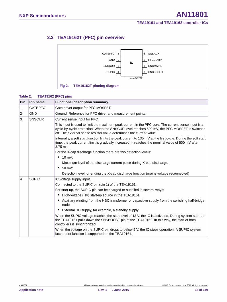
3.2 TEA19162T (PFC) pin overview
Fig 2. TEA19162T pinning diagram
Table 2. TEA19162 (PFC) pins
Pin Pin name Functional description summary
1 GATEPFC Gate driver output for PFC MOSFET.
2 GND Ground. Reference for PFC driver and measurement points.
3 SNSCUR Current sense input for PFC
This input is used to limit the maximum peak-current in the PFC core. The current sense input is a cycle-by-cycle protection. When the SNSCUR level reaches 500 mV, the PFC MOSFET is switched off. The external sense resistor value determines the current value.
Internally, a soft start function limits the peak current to 135 mV at the first cycle. During the soft start time, the peak current limit is gradually increased. It reaches the nominal value of 500 mV after 3.75 ms.
For the X-cap discharge function there are two detection levels:
• 10 mV:
Maximum level of the discharge current pulse during X-cap discharge.
• 50 mV:
Detection level for ending the X-cap discharge function (mains voltage reconnected)
4 SUPIC IC voltage supply input.
Connected to the SUPIC pin (pin 1) of the TEA19161.
For start-up, the SUPIC pin can be charged or supplied in several ways:
• High-voltage (HV) start-up source in the TEA19161
• Auxiliary winding from the HBC transformer or capacitive supply from the switching half-bridge node
• External DC supply, for example, a standby supply
When the SUPIC voltage reaches the start level of 13 V, the IC is activated. During system start-up, the TEA19161 pulls down the SNSBOOST pin of the TEA19162. In this way, the start of both controllers is synchronized.
When the voltage on the SUPIC pin drops to below 9 V, the IC stops operation. A SUPIC system latch reset function is supported on the TEA19161.
AN11801 All information provided in this document is subject to legal disclaimers. © NXP Semiconductors N.V. 2016. All rights reserved.
Application note Rev. 1 — 2 June 2016 13 of 140

NXP Semiconductors AN11801TEA19161 and TEA19162 controller ICs
5 SNSBOOST This pin combines two functions:
• It senses the boost voltage for regulation (output voltage of the PFC stage).
• It is used for communication between the TEA19161 and TEA19162 via internal current sources.
The SNSBOOST pin is externally connected to a resistive divided boost voltage. The resistor from SNSBOOST to GND must be 100 k. To ensure the intended functionality, the parallel capacitor must be 4.7 nF.
The SNSBOOST pin uses seven voltage levels:
• Short-pin or open-pin detection: Vscp(stop) = 0.4 V and Vscp(start) = 0.5 V. This function is also used by the TEA19161 to disable the IC if a protection is triggered or before start-up.
• Fast latch reset level: 2 V. To generate a fast latch reset in the TEA19161, the pin level is pulled high by a 200 A internal current source of the TEA19162.
• Regulation of the PFC output voltage in burst mode by the TEA19161. Soft start at 2.4 V and soft stop at 2.5 V.
• Control of the burst mode by TEA19161. Soft start at 2.4 V; soft stop at 2.5 V.
• Regulation of the PFC output voltage in normal operation: Vreg(SNSBOOST) = 2.5 V
• The pin voltage varies between 2.8 V and 3.23 V in the burst stop state of the burst mode operation of the TEA19161.
• PFC OVP (cycle-by-cycle): VOVP(SNSBOOST) 2.63 V (after a delay of 100 s)
The voltage levels on the SNSBOOST pin are influenced by:
• External resistive divider connected to the boost voltage
• Current sources in the TEA19162: 210 A; +35 nA; +100 A
• Current sources in the TEA19161: 6.4 A; +30 A; +110 A
6 SNSMAINS This pin combines two functions. The functions are alternately active in time during the same half-mains voltage cycle.
Mains voltage sensing
During the mains voltage sensing, the SNSMAINS pin is clamped to 0.25 V. The clamping of the SNSMAINS pin prevents that current leaks through the OTP network. There is no interference of the mains voltage measurement.
For mains sensing, the current flowing in the SNSMAINS pin is measured. The current depends on the external resistor value (typical 20 M and the mains voltage determine the amount of current. During a half-mains voltage cycle, the peak current value is determined and stored. The value is used as an input for:
• The mains compensation function of the PFC regulation loop
• The brownin and brownout functions
Table 2. TEA19162 (PFC) pins …continued
Pin Pin name Functional description summary
AN11801 All information provided in this document is subject to legal disclaimers. © NXP Semiconductors N.V. 2016. All rights reserved.
Application note Rev. 1 — 2 June 2016 14 of 140

NXP Semiconductors AN11801TEA19161 and TEA19162 controller ICs
The SNSMAINS current level is sensed continuously until the current level drops below 2.5 A. Then, the external temperature measurement starts.
At a current level of 5.75 A, the brownin level is reached and the IC starts switching. When the current drops again to below 5 A, the brownout level is reached and the IC switching stops.
When, after brownout, the brownin level is reached again, the latched protection state is reset.
If during 120 ms no positive dV/dt is detected, the X-capacitor discharge function is triggered. To reconnect the mains, the current on the SNSMAINS pin is monitored during the X-capacitor discharge mode.
External NTC Over Temperature Protection (OTP)
The OTP measurement lasts maximum 1 ms. During this time, a 200 A current flows from the pin through the external diode and NTC to ground. The resulting voltage on the pin is measured. When the voltage on the pin < 2 V at four consecutive measurement half-cycles, the OTP protection is activated.
7 PFCCOMP Frequency compensation for the PFC control-loop. Externally connected filter with typical values: 150 nF // (33 k + 470 nF).
The voltage on PFCCOMP is used to generate a soft stop behavior.
8 SNSAUX Sense input from an auxiliary winding of the PFC coil for:
• Demagnetization timing
• Valley detection to control the PFC switching
It is a 90 mV level with a time-out of 44.5 s.
To prevent damage of the input during surges (e.g. lightning), the auxiliary winding must be connected to the pin via an impedance (recommended is a 5.1 k series resistor).
Open-pin detection is possible using an internal pull-up current source.
Table 2. TEA19162 (PFC) pins …continued
Pin Pin name Functional description summary
AN11801 All information provided in this document is subject to legal disclaimers. © NXP Semiconductors N.V. 2016. All rights reserved.
Application note Rev. 1 — 2 June 2016 15 of 140

NXP Semiconductors AN11801TEA19161 and TEA19162 controller ICs
4. Application diagram
4.1 TEA19162
Fig 3. TEA19162 application diagram
AN11801 All information provided in this document is subject to legal disclaimers. © NXP Semiconductors N.V. 2016. All rights reserved.
Application note Rev. 1 — 2 June 2016 16 of 140

NXP Semiconductors AN11801TEA19161 and TEA19162 controller ICs
4.2 TEA19161T
5. Block diagram
5.1 TEA19162T
Fig 4. TEA19161 application diagram
AN11801 All information provided in this document is subject to legal disclaimers. © NXP Semiconductors N.V. 2016. All rights reserved.
Application note Rev. 1 — 2 June 2016 17 of 140

xxxxxxxxxxxxxxxxxxxxx xxxxxxxxxxxxxxxxxxxxxxxxxx xxxxxxx x x x xxxxxxxxxxxxxxxxxxxxxxxxxxxxxx xxxxxxxxxxxxxxxxxxx xx xx xxxxx xxxxxxxxxxxxxxxxxxxxxxxxxxx xxxxxxxxxxxxxxxxxxx xxxxxx xxxxxxxxxxxxxxxxxxxxxxxxxxxxxxxxxxx xxxxxxxxxxxx x x xxxxxxxxxxxxxxxxxxxxx xxxxxxxxxxxxxxxxxxxxxxxxxxxxxx xxxxx xxxxxxxxxxxxxxxxxxxxxxxxxxxxxxxxxxxxxxxxxxxxxxxxxx xxxxxxxx xxxxxxxxxxxxxxxxxxxxxxxxx xxxxxxxxxxxxxxxxxxxx xxx
AN
11801
Ap
plicatio
n n
ote
Rev. 1 —
2 Jun
e 2016
18 of 140
NX
P S
emico
nd
ucto
rsA
N11801
TE
A1
9161
an
d T
EA
191
62 c
on
trolle
r ICs
All inform
ation provided
in this docum
ent is subject to leg
al disclaim
ers.©
NX
P S
em
iconductors N
.V. 2016. A
ll rights reserved.
Fig 5. TEA19162 (PFC controller) block diagram

xxxxxxxxxxxxxxxxxxxxx xxxxxxxxxxxxxxxxxxxxxxxxxx xxxxxxx x x x xxxxxxxxxxxxxxxxxxxxxxxxxxxxxx xxxxxxxxxxxxxxxxxxx xx xx xxxxx xxxxxxxxxxxxxxxxxxxxxxxxxxx xxxxxxxxxxxxxxxxxxx xxxxxx xxxxxxxxxxxxxxxxxxxxxxxxxxxxxxxxxxx xxxxxxxxxxxx x x xxxxxxxxxxxxxxxxxxxxx xxxxxxxxxxxxxxxxxxxxxxxxxxxxxx xxxxx xxxxxxxxxxxxxxxxxxxxxxxxxxxxxxxxxxxxxxxxxxxxxxxxxx xxxxxxxx xxxxxxxxxxxxxxxxxxxxxxxxx xxxxxxxxxxxxxxxxxxxx xxx
AN
11801
Ap
plicatio
n n
ote
Rev. 1 —
2 Jun
e 2016
19 of 140
NX
P S
emico
nd
ucto
rsA
N11801
TE
A1
9161
an
d T
EA
191
62 c
on
trolle
r ICs
5.2 TEA19161T
All inform
ation provided
in this docum
ent is subject to leg
al disclaim
ers.©
NX
P S
em
iconductors N
.V. 2016. A
ll rights reserved.
Fig 6. TEA19161T (LLC controller) block diagram

NXP Semiconductors AN11801TEA19161 and TEA19162 controller ICs
6. Supply functions and start-up
6.1 Basic supply system overview
The TEA19161 has a high-voltage supply pin for start-up (SUPHV), a general supply (SUPIC), and an accurate regulated voltage output (SUPREG).
The SUPIC function can be used to supply the TEA19162 PFC controller IC. Start-up and protection levels are optimized to work as one system.
6.2 SUPHV high-voltage supply
To provide the SUPHV start-up source, the TEA19161 uses an external resistor. In this way, a high start-up current can be provided without too much power dissipation in the IC. It reduces the size of the IC die for low-cost design. Most of the power during start-up is located in the external resistor. To provide a start-up of approximately 0.5 s and generate sufficient MOSFET drive current during start-up RSUPHV is typical 24 k. The value of the mains voltage influences the behavior.
To handle the power during start-up and potential fault conditions, the external resistor RSUPHV must be selected. To handle the high voltage level in most applications, RSUPHV can include several SMD resistors in series.
The SUPHV pin also provides the IC supply in case of a latched protection and an off-state.
Fig 7. TEA1916 basic IC supply application
AN11801 All information provided in this document is subject to legal disclaimers. © NXP Semiconductors N.V. 2016. All rights reserved.
Application note Rev. 1 — 2 June 2016 20 of 140

NXP Semiconductors AN11801TEA19161 and TEA19162 controller ICs
6.2.1 Start-up via the SUPHV pin
Initially, the SUPHV source charges the capacitors on the SUPIC and SUPREG pins. The SUPHV pin is connected to Vboost. In the TEA19161, a high-voltage series switch is located between the SUPHV and SUPIC pins. From the SUPIC pin, an internal linear regulator supplies the SUPREG pin.
The SUPIC pin charge current is limited to 0.75 mA, until the voltage on the SUPIC pin reaches 3.5 V. When the voltage on the SUPIC pin exceeds 3.5 V, the Vboost voltage and the external resistor RSUPHV determine the charge current. However, to handle the power dissipation in the IC, the value of external resistor RSUPHV must limit the current to < 20 mA.
When the SUPIC reaches the 19.1 V start-up level, it is continuously regulated to this level with a hysteresis of 0.7 V. When the voltage on the SUPIC pin drops to below 19.1 V 0.7 V = 18.4 V, the switch between the SUPHV and SUPIC pins is activated.
When start-up is completed, regulation of the voltage on the SUPIC pin is ended. When the current taken from the SNSFB pin exceeds 63 A, it ends the start-up operation.
Fig 8. TEA19161 SUPHV, SUPIC, and SUPREG supply system
AN11801 All information provided in this document is subject to legal disclaimers. © NXP Semiconductors N.V. 2016. All rights reserved.
Application note Rev. 1 — 2 June 2016 21 of 140

NXP Semiconductors AN11801TEA19161 and TEA19162 controller ICs
During start-up, a number of other tasks are done:
• To make sure that the TEA19162 does not start operation before the complete system is ready for start-up, TEA19161 pulls low the voltage on the SNSBOOST pin.
• When the voltage on the SUPIC pin has reached the 19.1 V start-up level, the TEA19161 first reads all settings on the SNSOUT, GATELS, and SNSSET pins. When the reading of the settings is done, the voltage on the SNSBOOST pin is no longer pulled low. It is released.
• Before start-up is enabled, several signal levels are checked:
– The bias voltage on the SNSCUR and SNSCAP pins
– The voltage on the SNSBOOST pin must exceed 2.3 V
– Other protection levels
(1) SUPIC voltage
(2) SUPIC UVP (V)
(3) PFC output / 100 (V)
(4) HBC output voltage
(5) Low start-up current
(6) HV source (mA)
(7) SUPREG voltage
Fig 9. Typical start-up sequence (Vmains = 100 V (AC))
AN11801 All information provided in this document is subject to legal disclaimers. © NXP Semiconductors N.V. 2016. All rights reserved.
Application note Rev. 1 — 2 June 2016 22 of 140

NXP Semiconductors AN11801TEA19161 and TEA19162 controller ICs
6.2.2 SUPHV pin during burst mode operation
When the SUPIC voltage temporarily drops to a low value during burst mode, the SUPHV source can be activated. The voltage drop can happen, for example, when there is a long period of non-switching after a load step. In this situation, the supply from the auxiliary winding does not generate energy for a long time while the IC still takes a low amount of current.
When the SUPIC voltage drops to 14 V during the non-switching period of the burst mode, the HV source is activated. The SUPHV source regulates the SUPIC voltage between 14 V and 15 V. This emergency function prevents that the system stops and restarts because of an accidental condition. It triggers the SUPIC UVP level at 13.2 V.
6.2.3 SUPHV during protection
SUPHV supplies SUPIC during a latched protection state or a safe restart state. It regulates SUPIC between 19.1 V and 18.4 V by switching on/off the SUPHV supply.
During this state, resistor RSUPHV dissipates the power that can be calculated with the voltage drop and the average amount of current that is used by the TEA1916 ICs during that state. Figure 92 shows that four 1206-type SMD resistors are used for the RSUPHV function to handle the voltage and the power during protection.
Estimation of power in RSUPHV during protection with example values:
• Iprot(SUPIC) = 3.7 mA (TEA19161) + 0.2 mA (TEA19162) = 3.9 mA
• VBOOST = 380 V
• VSUPIC = 19 V
• PRSUPHV = (380 V 19 V) 3.9 mA = 1.4 W
(1) SUPIC voltage
(2) SUPIC UVP (V)
(3) PFC output / 100 (V)
(4) HBC output voltage
(5) Low start-up current
(6) HV source (mA)
(7) SUPREG voltage
Fig 10. Typical start-up sequence (Vmains = 230 V (AC))
AN11801 All information provided in this document is subject to legal disclaimers. © NXP Semiconductors N.V. 2016. All rights reserved.
Application note Rev. 1 — 2 June 2016 23 of 140

NXP Semiconductors AN11801TEA19161 and TEA19162 controller ICs
6.3 SUPIC supply using HBC transformer auxiliary winding
To obtain a supply voltage for the SUPIC pin during operation, an auxiliary winding on the HBC transformer can be used. As the SUPIC pin has a wide operational voltage range (13.2 V to 36 V), it is not a critical parameter.
However:
• To minimize power consumption, the voltage on the SUPIC pin must be low.
• During burst mode operation and because of the low current consumption of the supply, the bursts repetition frequency can become very low (e.g. at no output load). This behavior can cause an imbalance in the half-bridge switching, leading to a serious drop in the auxiliary supply for the SUPIC pin. To maintain the HBC load balance and avoid the extra SUPIC pin voltage drop, replace a single-side rectified auxiliary supply with a center-tapped construction. The center-tapped construction consists of two windings and two diodes.
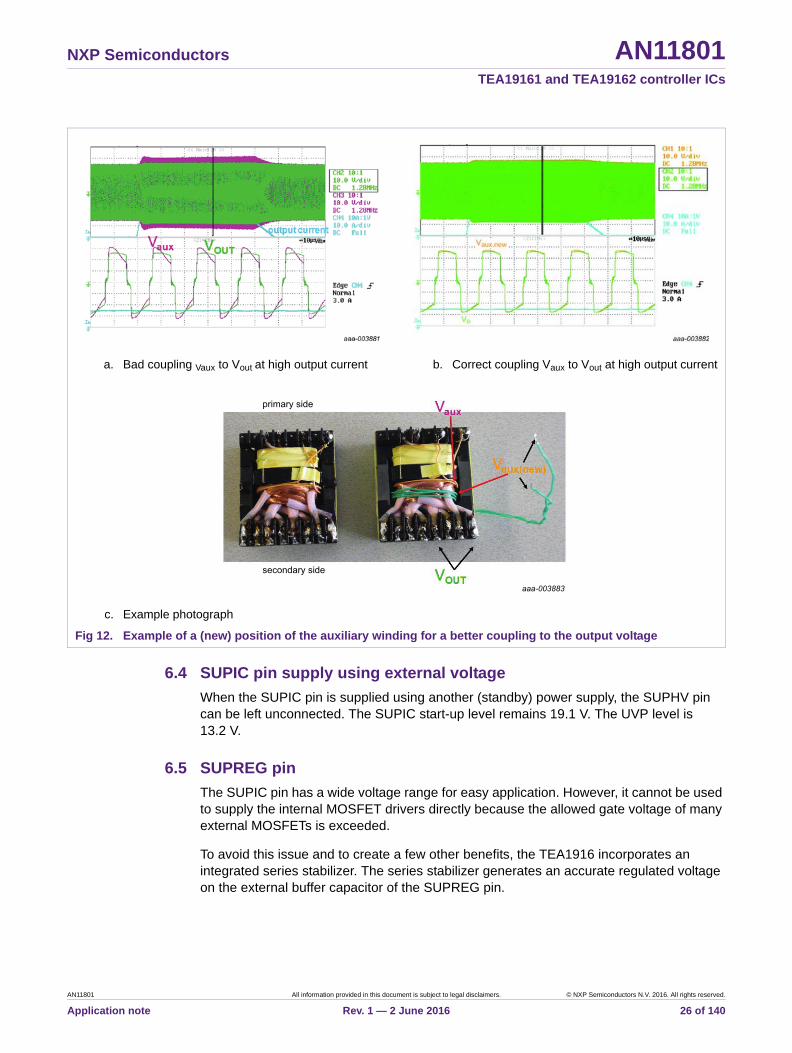
• To use the auxiliary winding voltage for the IC supply and for HBC output voltage measurement (using SNSOUT), the auxiliary winding supply must be an accurate representation of VO. To ensure a good coupling, place the transformer auxiliary winding physically on the secondary output side. When the transformer contains separate sections for primary and secondary winding (see Figure 11 and Figure 12), this aspect is more critical than on transformers that have all windings in one section.
• When mains insulation is included in the transformer, it can affect the auxiliary winding construction. When the transformer auxiliary winding is placed on the transformer construction secondary area, triple insulated wire is required.
In a combined SUPIC and SNSOUT function using a transformer auxiliary winding, a good representation of the output voltage for SNSOUT measurement can only be obtained after addressing several issues.
The advantage of a good coupling/representation of the auxiliary winding with the output windings is that a stable auxiliary voltage is obtained for the SUPIC pin. A low voltage on the SUPIC pin can be designed more easily for the lowest power consumption.
Fig 11. Transformer auxiliary winding on primary side (left, not preferred) and secondary side (right)
AN11801 All information provided in this document is subject to legal disclaimers. © NXP Semiconductors N.V. 2016. All rights reserved.
Application note Rev. 1 — 2 June 2016 24 of 140

NXP Semiconductors AN11801TEA19161 and TEA19162 controller ICs
6.3.1 SUPIC supply using HBC transformer auxiliary winding
The HBC output causes variation on an auxiliary winding supply. At peak current loads, the regulation compensates the voltage drop across the series components in the HBC output stage (resistance and diodes). The result is a higher voltage on the windings at higher output currents, because the higher currents cause a greater voltage drop across the series components.
In burst mode operation near no-load, the number of pulses in time that charge the SUPIC pin in time is limited. To prevent that the voltage drop severely, the rectifiers used in the auxiliary supply must be able to handle the high currents.
6.3.2 Voltage variations depending on auxiliary winding position: primary side component
VSNSOUT and/or VSUPIC can contain unwanted primary voltage because of less optimal position of the auxiliary winding. When the transformer contains separate sections for primary and secondary winding (see type in Figure 11 and Figure 12), this aspect is more critical than on transformers that have all windings in one section. This deviation can seriously endanger the feasibility of the SNSOUT sensing function. It can also have a serious effect on the SUPIC voltage.
To avoid a primary voltage component on the auxiliary voltage, the coupling of the auxiliary winding with the primary winding must be as small as possible. Place the auxiliary winding on the secondary windings and physically as remote as possible from the primary winding. Figure 12 shows the differences in results using comparison of the secondary side position.
AN11801 All information provided in this document is subject to legal disclaimers. © NXP Semiconductors N.V. 2016. All rights reserved.
Application note Rev. 1 — 2 June 2016 25 of 140
NXP Semiconductors AN11801TEA19161 and TEA19162 controller ICs
6.4 SUPIC pin supply using external voltage
When the SUPIC pin is supplied using another (standby) power supply, the SUPHV pin can be left unconnected. The SUPIC start-up level remains 19.1 V. The UVP level is 13.2 V.
6.5 SUPREG pin
The SUPIC pin has a wide voltage range for easy application. However, it cannot be used to supply the internal MOSFET drivers directly because the allowed gate voltage of many external MOSFETs is exceeded.
To avoid this issue and to create a few other benefits, the TEA1916 incorporates an integrated series stabilizer. The series stabilizer generates an accurate regulated voltage on the external buffer capacitor of the SUPREG pin.
a. Bad coupling Vaux to Vout at high output current b. Correct coupling Vaux to Vout at high output current
c. Example photograph
Fig 12. Example of a (new) position of the auxiliary winding for a better coupling to the output voltage
AN11801 All information provided in this document is subject to legal disclaimers. © NXP Semiconductors N.V. 2016. All rights reserved.
Application note Rev. 1 — 2 June 2016 26 of 140

NXP Semiconductors AN11801TEA19161 and TEA19162 controller ICs
The stabilized SUPREG voltage is used for:
• Supply of the internal low-side HBC driver
• Supply of the internal high-side driver using external components
• Supply for several internal circuits
• Reference voltage for optional external circuits
• Supply voltage for optional external circuits
The series stabilizer for the SUPREG pin is charged along with the SUPIC pin. To enable HBC operation, the SUPREG voltage must reach the regulation level of 11 V.
The SUPREG pin can provide a maximum total current of at least 30 mA.
It is important to realize that the SUPREG pin can only source current.
The drivers of GATELS and GATEPFC are supplied using the SUPREG pin. Depending on the operating condition, they draw current from it during operation. Depending on current load and temperature, small changes in value can be expected.
6.6 SUPHS pin
An external bootstrap buffer capacitor supplies the high-side driver. The bootstrap capacitor is connected between the high-side reference the HB pin and the high-side driver supply input the SUPHS pin. When HB is low, an external diode from the SUPREG pin charges this capacitor.
Selecting a suitable external diode can minimize the voltage drop between the SUPREG and SUPHS pins. Minimizing the voltage drop is important when using a MOSFET that requires a large amount of gate charge and/or when switching at high frequencies.
Remark: The current drawn from the SUPREG pin to charge CSUPHS, differs (in time and shape) from the current that the GATEPFC and GATELS drivers draw for each cycle.
6.6.1 Initial charging of the SUPHS pin
To charge CSUPHS using the bootstrap function, the GATELS switches on the low-side MOSFET at start-up.
The current taken from the SUPHS pin consists of two parts:
• Internal MOSFET driver GATEHS
• Internal circuit to control the GATEHS pin
6.6.2 A lower voltage SUPHS pin
Each time the half-bridge node (HB) is switched to ground level during normal operation, the bootstrap function charges CSUPHS. The voltage value between the HB and SUPHS pins is normally lower than the voltage on the SUPREG pin (or other bootstrap supply input) because of the voltage drop across the bootstrap diode.
The voltage drop across the bootstrap diode is directly related to the amount of current that is required to charge CSUPHS. The resulting voltage between the SUPHS and HB pins depends also on the available charge time.
AN11801 All information provided in this document is subject to legal disclaimers. © NXP Semiconductors N.V. 2016. All rights reserved.
Application note Rev. 1 — 2 June 2016 27 of 140
NXP Semiconductors AN11801TEA19161 and TEA19162 controller ICs
When an external MOSFET with a large gate capacitance must be switched at high frequency (high current + short time), a large voltage drop occurs.
During burst mode operation, voltages that are low or even too low can occur on the SUPHS pin. In burst mode, there are (long) periods of not switching. Therefore, long periods during which the SUPHS pin is not charged can occur. During this time, the circuit CSUPHS slowly discharges the supply voltage capacitor. When a new burst starts, the the voltage on the SUPHS pin is lower than during normal operation. During the first switching cycles, CSUPHS is recharged to its normal level. At low output power during burst mode, the switching frequency is normally relatively high. The high switching frequency limits fast recovery of the voltage between the SUPHS and HB pins.
Although in most applications the voltage drop is limited, it is an important issue for evaluation. The voltage drop can influence the selection of the best diode type for the bootstrap function. It can also influence the value of the SUPHS pin buffer capacitor.
When the voltage across CSUPHS drops to below 7 V, the driver stops operation to prevent unreliable switching.
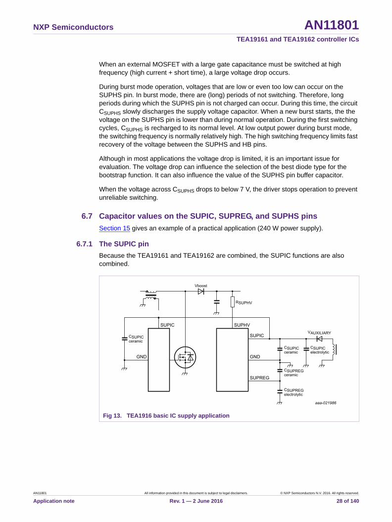
6.7 Capacitor values on the SUPIC, SUPREG, and SUPHS pins
Section 15 gives an example of a practical application (240 W power supply).
6.7.1 The SUPIC pin
Because the TEA19161 and TEA19162 are combined, the SUPIC functions are also combined.
Fig 13. TEA1916 basic IC supply application
AN11801 All information provided in this document is subject to legal disclaimers. © NXP Semiconductors N.V. 2016. All rights reserved.
Application note Rev. 1 — 2 June 2016 28 of 140

NXP Semiconductors AN11801TEA19161 and TEA19162 controller ICs
6.7.1.1 General
Use two types of capacitors on the SUPIC pin. An SMD ceramic type with a smaller value located close to both ICs and an electrolytic type incorporating the major part of the capacitance.
Typical values are:
• Electrolytic: CSUPIC = 47 F
• Ceramic capacitor near pin 1 of the TEA19161: CSUPIC = 470 nF
• Ceramic capacitor near pin 4 of the TEA19162: CSUPIC = 100 nF
6.7.1.2 Start-up
When an HV source provides the start-up energy, the SUPIC capacitor value can be small. However, it must be sufficient to handle the start-up during the 12 ms period between the start of the HBC pin and the auxiliary winding taking over the supply of the SUPIC pin.
Example of the basic value estimation:
• ISUPIC_start_HBC = 25 mA
• VSUPIC(startup) = Vstart(SUPIC) Vuvp(SUPIC) = 19.1 V 13 V = 5.9 V
• tvaux > 13 V = 12 ms; 12 ms is the time it takes for Vaux to exceed 13 V.
• Vboost(nom) = 390 V
• RSUPHV = 24 k
(1)
Example:
(2)
Example:
6.7.1.3 Normal operation
The main purpose of the capacitors on the SUPIC pin is to keep the current load variations (e.g. gate drive currents) locally at normal operation.
ISUPHV_start_HBC
Vboost nom VSUPIC startup –
RSUPHV----------------------------------------------------------------------=
ISUPHV_start_HBC390 V 19.2 V–
24 k------------------------------------- 15.45 mA= =
CSUPIC ISUPIC_start_HBC ISUPHV_start_HBC– tvaux
VSUPIC startup ----------------------------------------=
CSUPIC 25 mA 15.45 mA– 12 ms5.9 V--------------- 20 F= =
AN11801 All information provided in this document is subject to legal disclaimers. © NXP Semiconductors N.V. 2016. All rights reserved.
Application note Rev. 1 — 2 June 2016 29 of 140

NXP Semiconductors AN11801TEA19161 and TEA19162 controller ICs
6.7.1.4 Burst mode operation
When burst mode operation is applied, the supply construction often uses an auxiliary winding and start-up from the HV source. While in the burst mode, there is a long period during which the auxiliary winding is not able to charge CSUPIC. There is no HBC switching time between two bursts. The capacitor value on SUPIC must be large enough to keep the voltage above 13.2 V to prevent activating the SUPIC undervoltage stop level.
For efficiency reasons, it must also prevent that the SUPHV source is activated at 14 V.
Example of a value estimation:
(3)
(4)
6.7.2 Value of the capacitor for the SUPREG pin
SUPREG is the supply for the current of the HBC MOSFET drivers. Keeping current peaks local can be achieved using an SMD ceramic capacitor supported by an electrolytic capacitor. Keeping current peaks local is necessary to provide sufficient capacitance to prevent voltage drop during high current loads. To prevent significant voltage drop, the value of the capacitor on the SUPREG pin must be much higher than the (total) capacitance of the MOSFETs that must be driven. The total capacitance of the MOSFETS includes the SUPHS parallel load and capacitor bootstrap construction.
When considering the proper internal voltage regulator operation, the value of the capacitance on the SUPREG pin must be 1 F.
6.7.3 Value of the capacitor for the SUPHS pin
To support the charging of the gate of the high-side MOSFET, the capacitor for the SUPHS pin must be much larger than the gate capacitance. The higher capacitance prevents that a significant voltage drop occurs on the SUPHS pin because of the gate charge. When burst mode is applied, SUPHS is discharged by a small leakage current during the time between two bursts.
ISUPIC_between_2_bursts 1 mA=
VSUPIC burst Vaux burst Vlow SUPIC + 19 V 14 V– 5 V= = =
tbetween_2_bursts 40 ms=
CSUPIC ISUPIC_between_2_bursts
tbetween_2_bursts
VSUPIC burst ------------------------------------------- 1 mA
40 ms5 V
--------------- 8 F= =
AN11801 All information provided in this document is subject to legal disclaimers. © NXP Semiconductors N.V. 2016. All rights reserved.
Application note Rev. 1 — 2 June 2016 30 of 140

NXP Semiconductors AN11801TEA19161 and TEA19162 controller ICs
7. MOSFET drivers (GATELS, GATEHS, and GATEPFC)
The TEA1916 provides three outputs for driving external high-voltage power MOSFETs:
• GATEPFC for driving the PFC MOSFET (TEA19162)
• GATELS for driving the low side of the HBC MOSFET (TEA19161)
• GATEHS for driving the low side of the HBC MOSFET (TEA19161)
7.1 GATEPFC
To drive a high-voltage power MOSFET, the TEA19162 includes a strong output stage for PFC. The SUPIC pin supplies this output stage.
7.2 GATELS and GATEHS
Both TEA19161 drivers have identical driving capabilities for the gate of an external high-voltage power MOSFET. The low-side driver is referenced to the GND pin and is supplied from the SUPREG pin. The high-side driver has a floating connection to the midpoint of the external half-bridge. It is referenced to HB. The high-side driver is supplied using a capacitor on the SUPHS pin. The capacitor is supplied using an external bootstrap function of the SUPREG pin. When the low-side MOSFET is on, the bootstrap diode charges CSUPHS.
Both HBC drivers have a strong current source capability and an extra strong current sink capability. In general HBC operation, fast switch-on of the external MOSFET is not critical, as the HB node swings automatically to the correct state after switch-off. Fast switch-off, however, is important to limit switching losses and to prevent that a delay occurs, especially at high operating frequency.
Fig 14. Supply system for GATELS and GATEHS
AN11801 All information provided in this document is subject to legal disclaimers. © NXP Semiconductors N.V. 2016. All rights reserved.
Application note Rev. 1 — 2 June 2016 31 of 140

NXP Semiconductors AN11801TEA19161 and TEA19162 controller ICs
7.3 MOSFET drivers - General information
7.3.1 Switch-on
The time to switch on depends on:
• The supply voltage for the internal driver
• The characteristic of the internal driver
• Charging the gate capacitance
• The gate threshold voltage for the MOSFET that switches on
• The external circuit to the gate
7.3.2 Switch-off
The time to switch off depends on:
• The characteristic of the internal driver
• Discharging the gate capacitance
• The voltage on the gate just before discharge
• The gate threshold voltage for the MOSFET that switches off
• The external circuit to the gate
The internal driver can sink more current than it can source, because the timing for switching off the MOSFET is more critical than the time for switching it on. At higher frequencies and/or short on-time, timing becomes more critical for correct switching. Sometimes, a compromise must be made between fast switching and EMI effects. To optimize the switching behavior, a gate circuit between the driver output and the gate can be used.
The switching on/off of the MOSFETs with the drivers is approximated by alternating the charge and discharge of a MOSFET gate-source capacitance using a resistor (RDSon of the internal driver MOSFET and connections). The resistor value for discharging the gate is usually lower than for charging the gate.
Fig 15. Examples of three different gate circuits
AN11801 All information provided in this document is subject to legal disclaimers. © NXP Semiconductors N.V. 2016. All rights reserved.
Application note Rev. 1 — 2 June 2016 32 of 140

NXP Semiconductors AN11801TEA19161 and TEA19162 controller ICs
7.4 Specification of the gate drivers
The main function of the internal MOSFET drivers is to source and sink current to switch on/switch off the external MOSFET. To show the capability of the internal driver, the amount of current that can be sunk and sourced is specified.
The simplified model in Figure 16 demonstrates that the charge and discharge current values depend on the supply and gate voltage conditions. When the supply voltage is highest and the gate voltage 0 V, the source current value is highest. When the gate voltage is highest, the sink-current value is highest.
Fig 16. Simplified model of a MOSFET drive
Table 3. HBC and PFC driver specifications
Symbol Parameter Conditions Min Typ Max Unit
GATELS and GATEHS pins
Isource(GATEHS) source current on pin GATEHS
VGATEHS VHB = 4 V - 340 - mA
Isource(GATELS) source current on pin GATELS
VGATELS VGND = 4 V - 340 - mA
Isink(GATEHS) sink current on pin GATEHS VGATEHS VHB = 2 V - 580 - mA
VGATEHS VHB = 11 V - 2 - A
Isink(GATELS) sink current on pin GATELS VGATELS VGND = 2 V - 580 - mA
VGATELS VGND =11 V - 2 - A
Gate driver output (GATEPFC)
Isrc(GATEPFC) source current on pin GATEPFC
VGATEPFC = 2 V; VSUPIC 13 V - 0.6 - A
Isink(GATEPFC) sink current on pin GATEPFC
VGATEPFC = 2 V; VSUPIC 13 V - 0.6 - A
VGATEPFC = 10 V; VSUPIC 13 V - 1.4 - A
AN11801 All information provided in this document is subject to legal disclaimers. © NXP Semiconductors N.V. 2016. All rights reserved.
Application note Rev. 1 — 2 June 2016 33 of 140
NXP Semiconductors AN11801TEA19161 and TEA19162 controller ICs
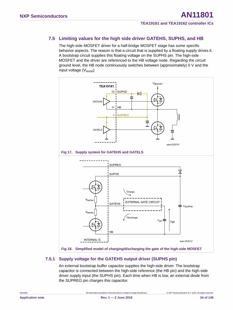
7.5 Limiting values for the high side driver GATEHS, SUPHS, and HB
The high-side MOSFET driver for a half-bridge MOSFET stage has some specific behavior aspects. The reason is that a circuit that is supplied by a floating supply drives it. A bootstrap circuit supplies this floating voltage on the SUPHS pin. The high-side MOSFET and the driver are referenced to the HB voltage node. Regarding the circuit ground level, the HB node continuously switches between (approximately) 0 V and the input voltage (Vboost)
7.5.1 Supply voltage for the GATEHS output driver (SUPHS pin)
An external bootstrap buffer capacitor supplies the high-side driver. The bootstrap capacitor is connected between the high-side reference (the HB pin) and the high-side driver supply input (the SUPHS pin). Each time when HB is low, an external diode from the SUPREG pin charges this capacitor.
Fig 17. Supply system for GATEHS and GATELS
Fig 18. Simplified model of charging/discharging the gate of the high-side MOSFET
AN11801 All information provided in this document is subject to legal disclaimers. © NXP Semiconductors N.V. 2016. All rights reserved.
Application note Rev. 1 — 2 June 2016 34 of 140

NXP Semiconductors AN11801TEA19161 and TEA19162 controller ICs
Instead of using the SUPREG pin as the power source for charging the SUPHS pin, another supply source can be used. In such a construction, it is important to check for correct start/stop sequences and to prevent that the SUPHS voltage exceeds 14 V (referenced to HB).
7.5.2 GATEHS switching
Figure 18 shows that current is taken from SUPHS when the external high side MOSFET is switched on. Switching on the internal high-side MOSFET, charges the gate of the external MOSFET (that can be represented as a capacitor Cgs) to a high voltage (Vgs). When the external MOSFET is switched off, the internal low-side MOSFET discharges Cgs.
The shape of the current is related to:
• The supply voltage for the internal driver (VSUPHS)
• The characteristic of the internal driver
• The gate capacitance to be charged
• The gate threshold voltage for the MOSFET
• The external circuit to the gate
• External parasitics
AN11801 All information provided in this document is subject to legal disclaimers. © NXP Semiconductors N.V. 2016. All rights reserved.
Application note Rev. 1 — 2 June 2016 35 of 140
NXP Semiconductors AN11801TEA19161 and TEA19162 controller ICs
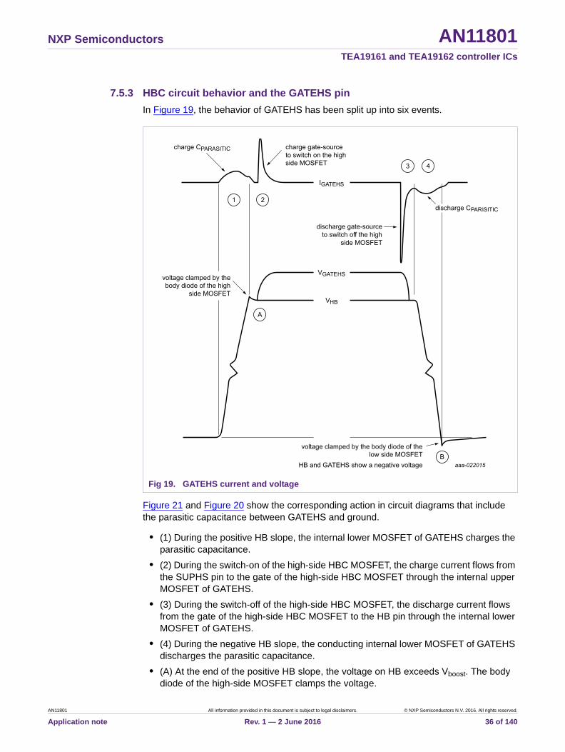
7.5.3 HBC circuit behavior and the GATEHS pin
In Figure 19, the behavior of GATEHS has been split up into six events.
Figure 21 and Figure 20 show the corresponding action in circuit diagrams that include the parasitic capacitance between GATEHS and ground.
• (1) During the positive HB slope, the internal lower MOSFET of GATEHS charges the parasitic capacitance.
• (2) During the switch-on of the high-side HBC MOSFET, the charge current flows from the SUPHS pin to the gate of the high-side HBC MOSFET through the internal upper MOSFET of GATEHS.
• (3) During the switch-off of the high-side HBC MOSFET, the discharge current flows from the gate of the high-side HBC MOSFET to the HB pin through the internal lower MOSFET of GATEHS.
• (4) During the negative HB slope, the conducting internal lower MOSFET of GATEHS discharges the parasitic capacitance.
• (A) At the end of the positive HB slope, the voltage on HB exceeds Vboost. The body diode of the high-side MOSFET clamps the voltage.
Fig 19. GATEHS current and voltage
AN11801 All information provided in this document is subject to legal disclaimers. © NXP Semiconductors N.V. 2016. All rights reserved.
Application note Rev. 1 — 2 June 2016 36 of 140
NXP Semiconductors AN11801TEA19161 and TEA19162 controller ICs
• (B) At the end of the negative HB slope, the voltage on the HB pin becomes negative. The body diode of the low-side MOSFET clamps the voltage to the ground level.
Fig 20. Current in GATEHS
AN11801 All information provided in this document is subject to legal disclaimers. © NXP Semiconductors N.V. 2016. All rights reserved.
Application note Rev. 1 — 2 June 2016 37 of 140
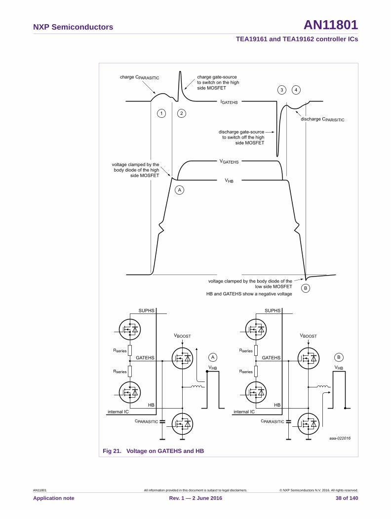
NXP Semiconductors AN11801TEA19161 and TEA19162 controller ICs
Fig 21. Voltage on GATEHS and HB
AN11801 All information provided in this document is subject to legal disclaimers. © NXP Semiconductors N.V. 2016. All rights reserved.
Application note Rev. 1 — 2 June 2016 38 of 140

NXP Semiconductors AN11801TEA19161 and TEA19162 controller ICs
7.5.4 Limiting values SUPHS and HB
The HB node and the SUPHS node are closely related because the internal high-voltage circuit is supplied with the voltage between these nodes. The voltage restrictions on the SUPHS pin are related to the limits for the voltage on the HB pin.
The values for HB can be derived from the voltage limits specified for the SUPHS pin using the practical voltage between both nodes: VSUPHS to VHB.
7.5.5 GATEHS limits
7.5.5.1 GATEHS voltage
The GATEHS voltage remains approximately within the voltage between the SUPHS and HB pins. In situation 1 (see Figure 20), the voltage on the GATEHS pin can become a little lower than the voltage on the HB pin, because of the conducting body diode. And at GATEHS switch-off, the voltage can become lower because of a ringing effect (see Section 7.6 and Table 4).
7.5.5.2 GATEHS current
Measurement setup
The behavior of the current in the GATEHS of a certain application can be checked. Because charging/discharging the parasitic capacitance causes the GATEHS current during the HB slopes, do not increase the parasitic capacitance too much at measurement setup.
Do not connect a voltage probe because it adds a relatively large capacitance (e.g. on GATEHS).
A current probe is suitable for measurement because it only adds a small amount of extra capacitance to the application circuit. Because of the small amount of extra capacitance added by a current probe, the measurement results show higher currents than in the original circuit.
The extra current can be measured by (temporarily) adding a second current probe. Measuring the difference in current values between one probe connected and two probes connected, the additional current caused by one probe can be found. Subtracting this probe-related current from the measurement result can provide more accurate values.
Table 4. Limiting values defined for VSUPHS, VHB, and VGATEHS
Symbol Parameter Conditions Min Max Unit
Voltages
VSUPHS voltage on pin SUPHS VHB VHB + 14 V
VHB voltage on pin HB maximum during mains surge; not repetitive
3 +700 V
t < 1 s 14 - V
VGATEHS voltage on pin GATEHS
VHB 0.4 VSUPHS + 0.4 V
AN11801 All information provided in this document is subject to legal disclaimers. © NXP Semiconductors N.V. 2016. All rights reserved.
Application note Rev. 1 — 2 June 2016 39 of 140

NXP Semiconductors AN11801TEA19161 and TEA19162 controller ICs
Current values
The SUPHS internal driver itself drives the currents in situations 2 and 3.
Another source causes the currents in situations 1 and 4. These currents must not become excessive. In situation 4, the GATEHS conducts to HB via the internal lower MOSFET of GATEHS. The peak current value may become similar to the discharge current without a problem. In situation 1, the GATEHS does not actively conduct, but the current flows through the body diode of the internal lower MOSFET of GATEHS. Normally, the peak current level in situation 1 is much lower than the discharge current of the same lower MOSFET in situation 3.
The expected value as a rule of thumb: .
At switch-off after situation 3, some parasitic ringing may occur. To check this condition for the gate drivers in general, see Section 7.6.
7.6 Gate driver switch off and limiting values
Parasitic inductance in the IC-to-MOSFET connections leads to a ringing effect after switch-off. A negative voltage and current occur in the gate driver pin. When designing the PBC layout, avoid long tracks. To prevent switching problems and stay within specification of the IC function, the resulting behavior must be checked.
The limiting voltage values in the TEA19161T data sheet (Ref. 1) only provide a safe minimum DC level of 0.4 V. However, if the level is not very high and the duration is short, the internal driver circuit can handle some extra reverse current.
7.6.1 Determining if switch-off reverse current is still safe
When a voltage measurement on the gate pin shows that the level is below 0.4 V, the current in the pin can be checked. In this way, how much energy the IC gate drive circuit contains can be seen. Because of several parasitic elements in the gate drive circuit (application) and the IC, a voltage measurement is often not conclusive.
The gate current must be checked using a DC current probe and an oscilloscope. Make sure that adding the current probe measurement does not (significantly) change the behavior of the circuit.
When all three conditions below are met, the reverse current is still safe:
• The reverse current does not exceed 300 mA (peak)
• The duration of pulses is shorter than 500 ns during each event
• The repetition rate of the events is lower than 200 kHz
This rule is valid for the GATELS and GATEHS pins (TEA19161) and for the GATEPFC pin (TEA19162).
Ipeak_in_1 0.25– Ipeak_in_3
AN11801 All information provided in this document is subject to legal disclaimers. © NXP Semiconductors N.V. 2016. All rights reserved.
Application note Rev. 1 — 2 June 2016 40 of 140

NXP Semiconductors AN11801TEA19161 and TEA19162 controller ICs
a. Circuit b. Measurement example
Fig 22. Ringing after GATE driver switch off
Fig 23. Example of checking if the gate driver reverse current is OK at switch off
AN11801 All information provided in this document is subject to legal disclaimers. © NXP Semiconductors N.V. 2016. All rights reserved.
Application note Rev. 1 — 2 June 2016 41 of 140

NXP Semiconductors AN11801TEA19161 and TEA19162 controller ICs
8. TEA19162 PFC functions
8.1 Mains voltage sensing and OTP (SNSMAINS pin)
The SNSMAINS pin combines two functions:
• The mains voltage sensing
• the sensing of an external NTC for detecting an OTP
The functions are alternatingly active in time. Each function is active during a half-mains voltage cycle.
Fig 24. Mains voltage sensing and OTP (SNSMAINS pin)
AN11801 All information provided in this document is subject to legal disclaimers. © NXP Semiconductors N.V. 2016. All rights reserved.
Application note Rev. 1 — 2 June 2016 42 of 140

NXP Semiconductors AN11801TEA19161 and TEA19162 controller ICs
8.2 Mains voltage sensing (SNSMAINS pin)
A resistor of typically 20 M connects one pole of the mains to the SNSMAINS pin. It allows the mains voltage measurement by sensing the current flowing into the SNSMAINS pin. During the mains measurement, an internal source clamps the SNSMAINS pin to 250 mV.
The mains current is tracked continuously. When the peak level is detected, the measured value is stored internally. The peak value is updated every half-mains measurement cycle (so, effectively every second half-mains cycle).
When the current value drops to below 2.5 A, the OTP measurement is activated. The mains current measurement is not active until the next half-mains half measurement cycle.
The measured current level is used for the brownout/brownin detection. The peak current level is used for the mains compensation in the PFC control loop.
The mains information is also used for starting and stopping the X-capacitor discharge and the latch reset functions.
Fig 25. Mains voltage sensing and OTP sensing alternating in time (SNSMAINS pin)
AN11801 All information provided in this document is subject to legal disclaimers. © NXP Semiconductors N.V. 2016. All rights reserved.
Application note Rev. 1 — 2 June 2016 43 of 140

NXP Semiconductors AN11801TEA19161 and TEA19162 controller ICs
8.3 Brownin and brownout (SNSMAINS pin)
At the SNSMAINS current level of 5.75 A, the PFC brownin level is detected and the PFC switching is started. At the 5 A current level, the brownout is detected and PFC stops switching.
When the current level drops to below the 5 A UVP level during operation, an internal timer of 50 ms is started. The current level must remain below 5 A for 50 ms before the UVP protection (brownout) is triggered.
This 50 ms time-filter is intended to prevent false triggering or accidental switch on-off-on sequences.
• Vmains(peak) = 1.41 VMAINS(rms)
• VSNSMAINS = 0.25 V
• Ibi = 5.75 A
• Ibo = 5 A
Requirement example: Vbi(rms) = 82 V
(5)
8.4 NTC measurement for external OTP (SNSMAINS pin)
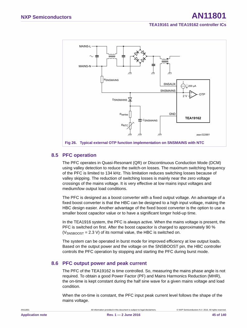
During the external OTP sensing period, the activated internal current source causes a 200 A flow out of the SNSMAINS pin, through the external diode, and NTC to the ground. The resulting voltage on pin is measured. When the voltage on the pin is below 2 V for four consecutive measurement cycles, the OTP protection is activated.
Figure 26 shows a typical application circuit.
The protection value of the NTC can be calculated with Equation 6:
(6)
With the required temperature level and the calculated NTC value, a suitable device can be selected. To optimize the protection function with the selected NTC type, the value of resistor Rseries can be modified.
RSNSMAINS
Vmains peak VSNSMAINS– Ibi
------------------------------------------------------------------- 1.41 82 V 0.25 V– 5.75 A
------------------------------------------------------- 20 M= = =
Vbo rms 1
1.41---------- 0.25 V Ibo RSNSMAINS+ 1
1.41---------- 0.25 V 5 A 20 M+ 71 V= = =
RNTC
Vdet SNSMAINS VFd–
Io SNSMAINS ---------------------------------------------------- Rseries
2 V 0.6 V–200 A
---------------------------- 3.3 k 3.8 k=–=–=
AN11801 All information provided in this document is subject to legal disclaimers. © NXP Semiconductors N.V. 2016. All rights reserved.
Application note Rev. 1 — 2 June 2016 44 of 140
NXP Semiconductors AN11801TEA19161 and TEA19162 controller ICs
8.5 PFC operation
The PFC operates in Quasi-Resonant (QR) or Discontinuous Conduction Mode (DCM) using valley detection to reduce the switch-on losses. The maximum switching frequency of the PFC is limited to 134 kHz. This limitation reduces switching losses because of valley skipping. The reduction of switching losses is mainly near the zero voltage crossings of the mains voltage. It is very effective at low mains input voltages and medium/low output load conditions.
The PFC is designed as a boost converter with a fixed output voltage. An advantage of a fixed boost converter is that the HBC can be designed to a high input voltage, making the HBC design easier. Another advantage of the fixed boost converter is the option to use a smaller boost capacitor value or to have a significant longer hold-up time.
In the TEA1916 system, the PFC is always active. When the mains voltage is present, the PFC is switched on first. After the boost capacitor is charged to approximately 90 % (VSNSBOOST = 2.3 V) of its normal value, the HBC is switched on.
The system can be operated in burst mode for improved efficiency at low output loads. Based on the output power and the voltage on the SNSBOOST pin, the HBC controller controls the PFC operation by stopping and starting the PFC during burst mode.
8.6 PFC output power and peak current
The PFC of the TEA19162 is time controlled. So, measuring the mains phase angle is not required. To obtain a good Power Factor (PF) and Mains Harmonics Reduction (MHR), the on-time is kept constant during the half sine wave for a given mains voltage and load condition.
When the on-time is constant, the PFC input peak current level follows the shape of the mains voltage.
Fig 26. Typical external OTP function implementation on SNSMAINS with NTC
AN11801 All information provided in this document is subject to legal disclaimers. © NXP Semiconductors N.V. 2016. All rights reserved.
Application note Rev. 1 — 2 June 2016 45 of 140

NXP Semiconductors AN11801TEA19161 and TEA19162 controller ICs
The highest peak current is an essential parameter for the PFC coil design. This current occurs at the lowest input voltage and maximum power.
The maximum peak current Ip(max) for a PFC operating in critical conduction mode can be calculated with Equation 7.
(7)
Example:
• Efficiency () = 0.9
• Po(nameplate) = 250 W
• Vmin (AC) = 90 V
The TEA1916 PFC operates in Quasi-Resonant (QR) mode with valley detection, providing good efficiency. Valley detection requires additional ringing time within every switching cycle. This ringing time adds short periods of no power transfer to the output capacitor. The system must compensate these periods using a higher peak current. A rule of thumb is that the peak current in QR mode is maximum 10 % higher than the calculated peak current in critical conduction mode.
8.7 PFC output voltage regulation (SNSBOOST pin)
A resistive divider between the PFC output voltage, the SNSBOOST pin and GND sets the boost output voltage value. When in regulation, the voltage on the SNSBOOST pine is kept at 2.5 V.
To support correct function for communication and burst mode operation, the resistor between the SNSBOOST and the GND pins must be 100 k. The TEA19161 and TEA19162 share the SNSBOOST pin is. Section 8.19 discusses the shared functions. Section 13 provides important PCB layout design information.
Ip max 2 2 Pi max
Vmin AC ----------------------------------
2 2Po nameplate
-------------------------------
Vmin AC ------------------------------------------------= =
Ip max 2 2 Pi max
Vmin AC ----------------------------------
2 2Po nameplate
-------------------------------
Vmin AC ------------------------------------------------
2 2250 W
0.9----------------
90 V--------------------------------- 8.73 A= = = =
Ip max 10 %+ 9.60 A=
Fig 27. PFC output regulation using the SNSBOOST pin
AN11801 All information provided in this document is subject to legal disclaimers. © NXP Semiconductors N.V. 2016. All rights reserved.
Application note Rev. 1 — 2 June 2016 46 of 140
NXP Semiconductors AN11801TEA19161 and TEA19162 controller ICs
The value of the resistors between the PFC output voltage and the SNSBOOST pin can be calculated with Equation 8:
(8)
Typical system values are:
• Rmeas(SNSBOOST) = 100 k
• Vreg(SNSBOOST) = 2.5 V
For example, To obtain a nominal PFC output voltage of Vboost = 390 V, Rboost must be 15.6 M.
8.8 PFC gate driver (GATEPFC pin)
The circuit that drives the gate of the power MOSFET has a high-current sourcing capability (Isource(GATEPFC)) of 0.6 A. It also has a high-current sink capability (Isink(GATEPFC)) of 1.4 A. To ensure efficient operation, the source and sink capabilities enable fast switch-on and switch-off of the external power MOSFET. To ensure a drive voltage of 11 V, the driver is supplied from the SUPIC pin via an internal voltage regulator.
Do not use active components like transistors to enhance switching behavior. They introduce arisk of bad switching behavior in special conditions.
8.9 PFC on-time control
The PFC operates under on-time control. The PFC MOSFET on-time is determined by:
• The error amplifier and the loop compensation using the voltage on the PFCCOMP pin. At 3.5 V, the on-time is reduced to zero. At 1.93 V, the on-time is at the maximum.
• Mains compensation using the voltage on the SNSMAINS pin.
In the TEA19162, the on-time is related to the voltage on the PFCCOMP and SNSMAINS pins. The relationship can be calculated with Equation 9:
(9)
8.10 PFC soft start and soft stop (SNSCUR and PFCCOM pins)
The PFC controller features a soft start function. The function slowly increases the primary peak current during start-up. The soft stop function slowly decreases the PFC peak current before operation is halted. These functions prevent audible noise of the PFC components (mainly the PFC coil) at start-up and during burst mode operation.
The soft start is included in the SNSCUR function (see Section 8.17) and the soft stop is included in the PFCCOMP function (see Section 8.11.4).
Rboost Rboost 1 Rboost 2 +=
Rboost Rmeas SNSBOOST Vboost Vreg SNSBOOST –
Vreg SNSBOOST -----------------------------------------------------------=
ton s 4603.5 V VPFCCOMP V –
ISNSMAINS A 2---------------------------------------------------------=
AN11801 All information provided in this document is subject to legal disclaimers. © NXP Semiconductors N.V. 2016. All rights reserved.
Application note Rev. 1 — 2 June 2016 47 of 140
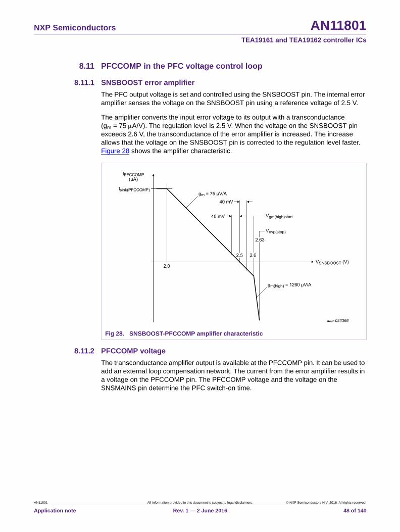
NXP Semiconductors AN11801TEA19161 and TEA19162 controller ICs
8.11 PFCCOMP in the PFC voltage control loop
8.11.1 SNSBOOST error amplifier
The PFC output voltage is set and controlled using the SNSBOOST pin. The internal error amplifier senses the voltage on the SNSBOOST pin using a reference voltage of 2.5 V.
The amplifier converts the input error voltage to its output with a transconductance (gm = 75 A/V). The regulation level is 2.5 V. When the voltage on the SNSBOOST pin exceeds 2.6 V, the transconductance of the error amplifier is increased. The increase allows that the voltage on the SNSBOOST pin is corrected to the regulation level faster. Figure 28 shows the amplifier characteristic.
8.11.2 PFCCOMP voltage
The transconductance amplifier output is available at the PFCCOMP pin. It can be used to add an external loop compensation network. The current from the error amplifier results in a voltage on the PFCCOMP pin. The PFCCOMP voltage and the voltage on the SNSMAINS pin determine the PFC switch-on time.
Fig 28. SNSBOOST-PFCCOMP amplifier characteristic
AN11801 All information provided in this document is subject to legal disclaimers. © NXP Semiconductors N.V. 2016. All rights reserved.
Application note Rev. 1 — 2 June 2016 48 of 140
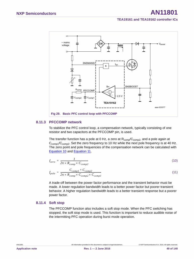
NXP Semiconductors AN11801TEA19161 and TEA19162 controller ICs
8.11.3 PFCCOMP network
To stabilize the PFC control loop, a compensation network, typically consisting of one resistor and two capacitors at the PFCCOMP pin, is used.
The transfer function has a pole at 0 Hz, a zero at Rcomp/Ccomp2, and a pole again at Ccomp1/Ccomp2. Set the zero frequency to 10 Hz while the next pole frequency is at 40 Hz. The zero point and pole frequencies of the compensation network can be calculated with Equation 10 and Equation 11.
(10)
(11)
A trade-off between the power factor performance and the transient behavior must be made. A lower regulation bandwidth leads to a better power factor but poorer transient behavior. A higher regulation bandwidth leads to a better transient response but a poorer power factor.
8.11.4 Soft stop
The PFCCOMP function also includes a soft stop mode. When the PFC switching has stopped, the soft stop mode is used. This function is important to reduce audible noise of the intermitting PFC operation during burst mode operation.
Fig 29. Basic PFC control loop with PFCCOMP
fzero1
2 Rcomp Ccomp2---------------------------------------------------=
fpole
Ccomp1 Ccomp2+
2 Rcomp Ccomp2 Ccomp1---------------------------------------------------------------------------=
AN11801 All information provided in this document is subject to legal disclaimers. © NXP Semiconductors N.V. 2016. All rights reserved.
Application note Rev. 1 — 2 June 2016 49 of 140

NXP Semiconductors AN11801TEA19161 and TEA19162 controller ICs
During soft stop, an additional internal circuit sets the PFCCOMP voltage. The output voltage of the SNSBOOST transconductance amplifier is disconnected. To reduce the PFC on-time, an internal current source of 30 A charges the PFCCOMP network to a higher voltage. When the PFCCOMP voltage has reached 3.5 V, the soft stop ends (zero on-time).
8.12 Mains compensation in the PFC voltage control loop
The PFC transfer function, from which the PFC on-time can be derived, is inversely proportional to the squared mains input voltage (see Figure 29).
(12)
In a typical application, the result is a low bandwidth for low mains input voltages. At high mains input voltages, the MHR requirements can be hard to meet.
To compensate for the mains input voltage influence, the TEA19162 contains a correction circuit. The peak mains voltage is measured at the SNSMAINS pin. It is used for the internal compensation. Figure 31 shows the relationship between the SNSMAINS voltage, the PFCCOMP voltage and the on-time according to Equation 9.
Fig 30. Soft stop function on PFCCOMP
K Vmains A
Vmains2
------------------=
AN11801 All information provided in this document is subject to legal disclaimers. © NXP Semiconductors N.V. 2016. All rights reserved.
Application note Rev. 1 — 2 June 2016 50 of 140

NXP Semiconductors AN11801TEA19161 and TEA19162 controller ICs
8.13 PFC demagnetization sensing (SNSAUX pin)
The voltage on the SNSAUX pin is used to detect transformer demagnetization. During the secondary stroke, the transformer is magnetized and current flows to the boost output. During this time, the SNSAUX voltage is lower than 90 mV and the PFC MOSFET remains switched off.
When the transformer is demagnetized and the current stops flowing to the boost output, the SNSAUX voltage exceeds 90 mV and valley detection is started. The MOSFET remains off until a valley is detected.
To ensure that switching continues under all circumstances, the MOSFET is forced to switch on if the magnetization of the transformer is not detected within 44.5 s after the GATEPFC pin goes LOW.
8.14 PFC valley sensing (SNSAUX pin)
If the voltage at the MOSFET drain is at its minimum (valley switching), the PFC MOSFET is switched on for the next stroke. This action reduces switching losses and EMI (see Figure 32).
The valley sensing on the SNSAUX pin detects the valleys. It measures the voltage on the auxiliary winding of the PFC coil. This signal is a scaled and inverted copy of the MOSFET drain voltage. When a valley of the drain voltage (= top of the SNSAUX voltage) is detected, the MOSFET is switched on for the next cycle.
If no valley is detected within 44.5 s after demagnetization, the MOSFET is forced to switch on.
(1) VPFCCOMP = 2 V
(2) VPFCCOMP = 2.5 V
(3) VPFCCOMP = 3 V
(4) VPFCCOMP = 3.5 V
(5) Minimum ISNSMAINS for normal operation
Fig 31. On-time at different voltages on the PFCCOMP pin
AN11801 All information provided in this document is subject to legal disclaimers. © NXP Semiconductors N.V. 2016. All rights reserved.
Application note Rev. 1 — 2 June 2016 51 of 140
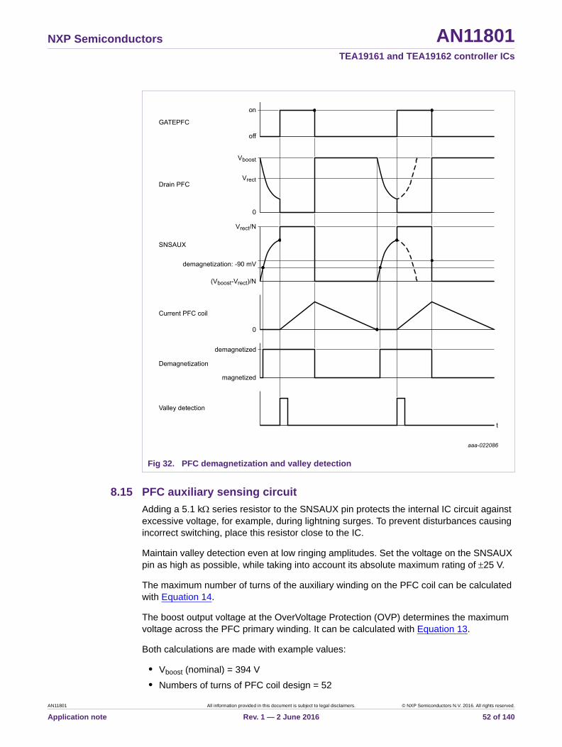
NXP Semiconductors AN11801TEA19161 and TEA19162 controller ICs
8.15 PFC auxiliary sensing circuit
Adding a 5.1 k series resistor to the SNSAUX pin protects the internal IC circuit against excessive voltage, for example, during lightning surges. To prevent disturbances causing incorrect switching, place this resistor close to the IC.
Maintain valley detection even at low ringing amplitudes. Set the voltage on the SNSAUX pin as high as possible, while taking into account its absolute maximum rating of 25 V.
The maximum number of turns of the auxiliary winding on the PFC coil can be calculated with Equation 14.
The boost output voltage at the OverVoltage Protection (OVP) determines the maximum voltage across the PFC primary winding. It can be calculated with Equation 13.
Both calculations are made with example values:
• Vboost (nominal) = 394 V
• Numbers of turns of PFC coil design = 52
Fig 32. PFC demagnetization and valley detection
AN11801 All information provided in this document is subject to legal disclaimers. © NXP Semiconductors N.V. 2016. All rights reserved.
Application note Rev. 1 — 2 June 2016 52 of 140
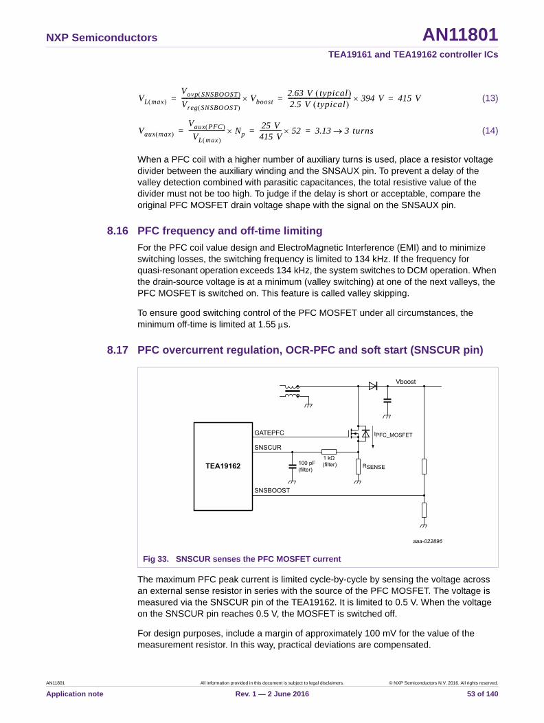
NXP Semiconductors AN11801TEA19161 and TEA19162 controller ICs
(13)
(14)
When a PFC coil with a higher number of auxiliary turns is used, place a resistor voltage divider between the auxiliary winding and the SNSAUX pin. To prevent a delay of the valley detection combined with parasitic capacitances, the total resistive value of the divider must not be too high. To judge if the delay is short or acceptable, compare the original PFC MOSFET drain voltage shape with the signal on the SNSAUX pin.
8.16 PFC frequency and off-time limiting
For the PFC coil value design and ElectroMagnetic Interference (EMI) and to minimize switching losses, the switching frequency is limited to 134 kHz. If the frequency for quasi-resonant operation exceeds 134 kHz, the system switches to DCM operation. When the drain-source voltage is at a minimum (valley switching) at one of the next valleys, the PFC MOSFET is switched on. This feature is called valley skipping.
To ensure good switching control of the PFC MOSFET under all circumstances, the minimum off-time is limited at 1.55 s.
8.17 PFC overcurrent regulation, OCR-PFC and soft start (SNSCUR pin)
The maximum PFC peak current is limited cycle-by-cycle by sensing the voltage across an external sense resistor in series with the source of the PFC MOSFET. The voltage is measured via the SNSCUR pin of the TEA19162. It is limited to 0.5 V. When the voltage on the SNSCUR pin reaches 0.5 V, the MOSFET is switched off.
For design purposes, include a margin of approximately 100 mV for the value of the measurement resistor. In this way, practical deviations are compensated.
VL max Vovp SNSBOOST
Vreg SNSBOOST --------------------------------------- Vboost 2.63 V typical
2.5 V typical ----------------------------------------- 394 V 415 V= = =
Vaux max Vaux PFC
VL max ------------------------ Np 25 V
415 V-------------- 52 3.13 3 turns= = =
Fig 33. SNSCUR senses the PFC MOSFET current
AN11801 All information provided in this document is subject to legal disclaimers. © NXP Semiconductors N.V. 2016. All rights reserved.
Application note Rev. 1 — 2 June 2016 53 of 140

NXP Semiconductors AN11801TEA19161 and TEA19162 controller ICs
Example:
(15)
Because of the discharging of the MOSFET drain capacitance, a voltage peak appears on the SNSCUR pin when the PFC MOSFET is switched on during a switching cycle. The leading-edge blanking time of 300 ns ensures that the overcurrent sensing function does not react to this transitory peak.
To minimize audible noise at start-up or restart, a soft start function is included in the SNSCUR pin. The OCR level is modified for this soft start function, starting with 135 mV. This level is gradually increased to the regular 500 mV within 3.75 ms. The PFC on-time increases accordingly.
8.18 Active X-capacitor discharge
The TEA19162T provides an active X-capacitor discharge function with a special PFC MOSFET operation mode.
To suppress electromagnetic interference in most applications, a filter is required on the mains input. In addition to an inductance, EMI filters typically include one or more X-capacitors connected between the mains input terminals.
The active X-capacitor discharge function reduces the voltage between the device mains terminals to a safe value within a certain time period after the device is disconnected from the mains. In some regulatory regimes, this reduction is mandatory. If the voltage is not reduced, inadvertently contacting the terminals of the plug can cause an electrical shock.
Fig 34. Soft start SNSCUR pin
Rsense PFC Vocr SNSCUR 100 mV–
Ip max ---------------------------------------------------------- 500 mV 100 mV–
8.73 Ap--------------------------------------------- 46 m= = =
AN11801 All information provided in this document is subject to legal disclaimers. © NXP Semiconductors N.V. 2016. All rights reserved.
Application note Rev. 1 — 2 June 2016 54 of 140

NXP Semiconductors AN11801TEA19161 and TEA19162 controller ICs
In most applications, resistors between the mains connections provide the discharge function. This resistive path always takes some power from the mains during operation. In the TEA1916 concept, these resistors are not required. To limit circuit current consumption during operation, the TEA19162 only activates the discharge function when required. It improves the no-load and low-load power consumption performance.
The SNSMAINS mains sensing function monitors the input voltage every cycle. When mains disconnection is detected, a special operation mode for the PFC MOSFET discharges the X-capacitors and the output capacitor of the bridge rectifier.
8.18.1 Start active X-capacitor discharge
After the mains voltage is disconnected, the active X-capacitor discharge function is activated.
When the mains input voltage (and so also the measured current into the SNSMAINS pin) increases during the mains measurement, the system assumes the presence of a mains voltage. When the mains voltage does not increase (no positive dV/dt) for a minimum period of 120 ms, the X-capacitor discharge function is activated. The minimum period of 120 ms is measured starting from the time when mains peak is reached.
When the active X-capacitor discharge function is activated, the X-capacitor is discharged in a special operating mode of an external PFC MOSFET (see Figure 35 and Figure 36).
8.18.2 X-capacitor discharge via a PFC MOSFET operation
During the PFC MOSFET operation for discharging the X-capacitor, several internal functions are used:
• SNSMAINS to detect when the mains voltage is interrupted or switched on again
• SNSCUR to measure the discharge current during each cycle
• GATEPFC to charge and discharge the gate of the external PFC MOSFET and to measure the resulting voltage on the GATEPFC pin
Fig 35. X-capacitor discharge with a PFC MOSFET discharge mode
AN11801 All information provided in this document is subject to legal disclaimers. © NXP Semiconductors N.V. 2016. All rights reserved.
Application note Rev. 1 — 2 June 2016 55 of 140
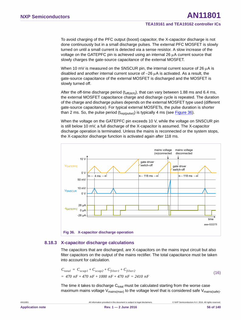
NXP Semiconductors AN11801TEA19161 and TEA19162 controller ICs
To avoid charging of the PFC output (boost) capacitor, the X-capacitor discharge is not done continuously but in a small discharge pulses. The external PFC MOSFET is slowly turned on until a small current is detected via a sense resistor. A slow increase of the voltage on the GATEPFC pin is achieved using an internal 26 A current source that slowly charges the gate-source capacitance of the external MOSFET.
When 10 mV is measured on the SNSCUR pin, the internal current source of 26 A is disabled and another internal current source of 26 A is activated. As a result, the gate-source capacitance of the external MOSFET is discharged and the MOSFET is slowly turned off.
After the off-time discharge period (toff(dch)), that can vary between 1.88 ms and 6.4 ms, the external MOSFET capacitance charge and discharge cycle is repeated. The duration of the charge and discharge pulses depends on the external MOSFET type used (different gate-source capacitance). For typical external MOSFETs, the pulse duration is shorter than 2 ms. So, the pulse period (trep(pulse)) is typically 4 ms (see Figure 36).
When the voltage on the GATEPFC pin exceeds 10 V, while the voltage on SNSCUR pin is still below 10 mV, a full discharge of the X-capacitor is assumed. The X-capacitor discharge operation is terminated. Unless the mains is reconnected or the system stops, the X-capacitor discharge function is activated again after 118 ms.
8.18.3 X-capacitor discharge calculations
The capacitors that are discharged, are X-capacitors on the mains input circuit but also filter capacitors on the output of the mains rectifier. The total capacitance must be taken into account for calculation.
(16)
The time it takes to discharge Ctotal must be calculated starting from the worse case maximum mains voltage Vmains(max) to the voltage level that is considered safe Vmains(safe).
Fig 36. X-capacitor discharge operation
Ctotal Cxcap1 Cxcap2 Cfilter1 Cfilter2+ + +=
470= nF 470 nF 1000 nF 470 nF 2410 nF=+ + +
AN11801 All information provided in this document is subject to legal disclaimers. © NXP Semiconductors N.V. 2016. All rights reserved.
Application note Rev. 1 — 2 June 2016 56 of 140

NXP Semiconductors AN11801TEA19161 and TEA19162 controller ICs
• Vmains(safe) = 138 V
• Vmains(max) = 373 V
There is a time delay between the moment that the mains disconnection is detected and the moment that the X-cap discharge starts.
• td(dch)xcap = 118 ms
The average discharge current can be estimated as given in Section 8.18.3.1.
• Idch(AV) = 1.43 mA
The time to discharge can be calculated with Equation 17
(17)
8.18.3.1 Estimation of average discharge current
The peak current during discharge can be calculated with the charge stop level on the SNSCUR pin and the value of the SNSCUR sense resistor.
(18)
The properties of the PFC MOSFET must be used to determine the duration of one discharge pulse. Here MOSFET example characteristics are used:
• Gate capacitance: Ciss = 1750 pF
• Gate threshold for conducting: Vth = 4.0 V
• Gate voltage for reaching Idch(peak): Vpeak = 4.5 V
This voltage is often not accurately specified. So, a best estimation must be used. The estimation value can be checked in the application.
With these values, a MOSFET constant for conduction can be defined.
(19)
The time for charging and discharging the MOSFET gate is the same:
.
(20)
The average current during one pulse can be calculated with Equation 21:
tdch tdch xcap Ctotal Vmains max Vmains safe –
Idch AV ---------------------------------------------------------------------------------------+=
118= ms 2410 nF 373 V 138 V– 1.43 mA
-------------------------------------------------------------------- 516 ms=+
Idch peak Vstop ch SNSCUR
Rm--------------------------------------- 10 mV
40 m----------------- 250 mA= = =
KIdch-Vgs
Idch peak
Vpeak Vth– 2---------------------------------- 250 mA
4.5 V 4 V– 2----------------------------------- 1 A/V
2= = =
Ich GATEPFC Idch GATEPFC 26 A= =
tVth
Ciss VthIch GATEPFC -------------------------------- 1750 pF 4 V
26 A------------------------------------ 269 s= = =
tVpeak
Ciss VpeakIch GATEPFC -------------------------------- 1750 pF 4.5 V
26 A---------------------------------------- 303 s= = =
AN11801 All information provided in this document is subject to legal disclaimers. © NXP Semiconductors N.V. 2016. All rights reserved.
Application note Rev. 1 — 2 June 2016 57 of 140

NXP Semiconductors AN11801TEA19161 and TEA19162 controller ICs
(21)
The average current during the complete discharge period includes the off-time.
• trep(pulse) = 4 ms
(22)
8.18.4 Reconnecting the mains voltage while discharging
A positive dV/dt on the SNSMAINS pin detects the reconnected mains. If the mains is reconnected while the GATEPFC pin discharges the X-capacitor, the current through the external MOSFET rapidly increases to exceed 10 mV. When the voltage on SNSCUR exceeds 50 mV, the X-capacitor discharge function is terminated. At the same time, the internal driver for an external MOSFET is brought from the high-impedance mode to a normal operation mode. So, the external MOSFET is turned off like it is during normal operation.
8.18.5 Disabling X-capacitor discharge function
The X-capacitor discharge function can be disabled by adding a DC offset that exceeds 10 mV on the SNSCUR pin. Adding a DC offset can be done using a resistor connected to the SUPREG pin (see Figure 37). This small offset has a minor effect on the regular current sensing during operation and soft start.
Ipulse AV 13---
Vpeak
tVpeak--------------
2tVpeak tVth– 2 KIdch-Vgs=
13--- 4.5 V
303 s----------------- 2
303 s 269 s– 2 1 A/V2
83.3 mA=
tdch AV Ipulse AV 2 tVpeak tVth–
trep pulse ------------------------------------------------------------------------=
83.3 mA 2 303 s 269 s– 4 ms
---------------------------------------------------------------------------------- 1.42 mA==
Fig 37. Disabling the X-capacitor discharge function
AN11801 All information provided in this document is subject to legal disclaimers. © NXP Semiconductors N.V. 2016. All rights reserved.
Application note Rev. 1 — 2 June 2016 58 of 140

NXP Semiconductors AN11801TEA19161 and TEA19162 controller ICs
8.19 PFC burst mode
Based on the output power and feedback level of the HBC converter, the HBC controller decides when the PFC enters the burst mode. Based on the SNSBOOST voltage level and the power requirement on the output, the HBC controller decides when the PFC starts switching and stops switching.
To provide the correct communication levels, the resistor from the SNSBOOST pin to GND must be 100 k. In parallel, a noise suppression capacitor can be applied. The value of this capacitor must not affect the dynamic behavior too much. A few nanofarads are recommended.
8.19.1 PFC start and stop
8.19.1.1 Stop PFC
An internal current source of 6.4 A in the TEA19161 HBC controller controls the PFC burst mode operation. When the current source is active, it lifts the voltage on the SNSBOOST pin and the PFC controller stops switching. Because the resistor on SNSBOOST is 100 k, the voltage increases by 100 k 5 A = 500 mV. Initially, the level increases from 2.5 V (normal regulation level) to 3 V. In burst mod, the voltage levels on the SNSBOOST pin slightly deviate because of the dynamic behavior.
8.19.1.2 Start PFC
While the PFC is not switching, the PFC output voltage decreases. The voltage on the SNSBOOST pin also decreases. When the SNSBOOST voltage decreases 100 mV, the HBC controller switches off the internal current source. So, the voltage on the SNSBOOST pin drops to below 2.8 V and PFC starts switching again.
8.19.1.3 Stop PFC (burst mode)
During the PFC switching in burst mode, the PFC output voltage increases again. When the SNSBOOST voltage reaches 2.37 V, the HBC controller switches on the current source to pull up the voltage on the SNSBOOST pin. The PFC stops switching. To minimize audible noise, the PFC starts and stops using a soft start and soft stop procedure.
8.19.2 SNSBOOST levels
• 3.25 V
Overvoltage protection level in burst mode after the burst switching has ended with a soft stop.
• 2.8 V to 3.25 V
The voltage range in PFC burst mode when HBC current source is active. The PFC does not switch and the PFC output voltage and the HBC current source set the voltage on the SNSBOOST pin.
• 2.8 V
Start PFC switching in burst mode. The HBC controller disables the current source to start PFC burst mode switching with a soft start.
• 2.63 V
AN11801 All information provided in this document is subject to legal disclaimers. © NXP Semiconductors N.V. 2016. All rights reserved.
Application note Rev. 1 — 2 June 2016 59 of 140

NXP Semiconductors AN11801TEA19161 and TEA19162 controller ICs
PFC overvoltage protection. When the SNSBOOST reaches the OVP level during operation (PFC switching), the switching is stopped. The OVP function has a delay of 100 s for general purposes and to prevent interference in burst mode during the transition from switching to not switching.
• 2.5 V
Regulation level of the internal error amplifier during PFC operation.
• 2.37 V
PFC stops switching in burst mode. The HBC controller enables the internal current source to stop PFC switching with a soft stop.
• 2.0 V
Latched protection reset level.
• 0.4 V
PFC open-loop protection.
a. Block diagram
b. Timing diagram
Fig 38. PFC burst mode control using the SNSBOOST pin
AN11801 All information provided in this document is subject to legal disclaimers. © NXP Semiconductors N.V. 2016. All rights reserved.
Application note Rev. 1 — 2 June 2016 60 of 140
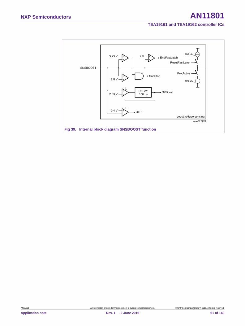
NXP Semiconductors AN11801TEA19161 and TEA19162 controller ICs
Fig 39. Internal block diagram SNSBOOST function
AN11801 All information provided in this document is subject to legal disclaimers. © NXP Semiconductors N.V. 2016. All rights reserved.
Application note Rev. 1 — 2 June 2016 61 of 140

NXP Semiconductors AN11801TEA19161 and TEA19162 controller ICs
9. HBC (TEA19161)
9.1 HBC start and SNSBOOST UVP
To ensure proper working of the HBC, the TEA19161T starts operating when the input voltage is higher than approximately 90 % of the nominal boost voltage (VSNSBOOST(nom) = 2.3 V). For the TEA19161T to start operating, the SUPIC start level must also be reached and the initial procedures completed.
The voltage on the SNSBOOST pin is sensed continuously. When the voltage on the SNSBOOST pin drops to below 1.6 V and the low-side MOSFET is on, HBC switching is stopped. When the SNSBOOST voltage exceeds the start level of 2.3 V, the HBC starts/restarts.
9.2 Power regulation using Vcap control
The TEA19161 uses the voltage across the resonant capacitor (VSNSCAP) to control the output power. VSNSCAP has a linear relation with the output power. The voltage changes on the resonant capacitor are a result of the primary current that drives the power conversion.
The power can be controlled by switching off the gate drive at a certain VSNSCAP. The adaptive non-overlap function drives the gate drive switch-on.
The system feedback drives the VSNSCAP levels for higher power or lower power.
AN11801 All information provided in this document is subject to legal disclaimers. © NXP Semiconductors N.V. 2016. All rights reserved.
Application note Rev. 1 — 2 June 2016 62 of 140

NXP Semiconductors AN11801TEA19161 and TEA19162 controller ICs
a. Curve
b. Circuit
Fig 40. Vcap power control: switch-off at the required VSNSCAP voltage level (Vls(SNSCAP) and Vls(SNSCAP)
AN11801 All information provided in this document is subject to legal disclaimers. © NXP Semiconductors N.V. 2016. All rights reserved.
Application note Rev. 1 — 2 June 2016 63 of 140
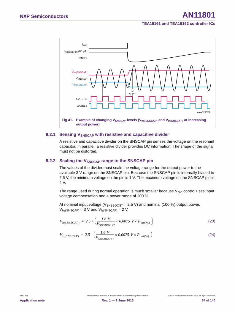
NXP Semiconductors AN11801TEA19161 and TEA19162 controller ICs
9.2.1 Sensing VSNSCAP with resistive and capacitive divider
A resistive and capacitive divider on the SNSCAP pin senses the voltage on the resonant capacitor. In parallel, a resistive divider provides DC information. The shape of the signal must not be distorted.
9.2.2 Scaling the VSNSCAP range to the SNSCAP pin
The values of the divider must scale the voltage range for the output power to the available 3 V range on the SNSCAP pin. Because the SNSCAP pin is internally biased to 2.5 V, the minimum voltage on the pin is 1 V. The maximum voltage on the SNSCAP pin is 4 V.
The range used during normal operation is much smaller because Vcap control uses input voltage compensation and a power range of 200 %.
At nominal input voltage (VSNSBOOST = 2.5 V) and nominal (100 %) output power, Vhs(SNSCAP) = 3 V and Vls(SNSCAP) = 2 V.
(23)
(24)
Fig 41. Example of changing VSNSCAP levels (Vhs(SNSCAP) and Vls(SNSCAP) at increasing output power)
Vhs SNSCAP 2.51.6 V
VSNSBOOST--------------------------- 0.0075 V Pout % +=
Vls SNSCAP 2.51.6 V
VSNSBOOST--------------------------- 0.0075 V Pout % –=
AN11801 All information provided in this document is subject to legal disclaimers. © NXP Semiconductors N.V. 2016. All rights reserved.
Application note Rev. 1 — 2 June 2016 64 of 140

NXP Semiconductors AN11801TEA19161 and TEA19162 controller ICs
The converter regulation of the SNSFB pin corrects any deviations in the regulation chain. The actual Vhs(SNSCAP) and Vls(SNSCAP) levels can therefore deviate from the ideal values that are used for the nominal design.
These levels are valid for the HP mode. Below a preset power level, the LP mode is entered and the levels are recalculated to fit the correct Vhs(SNSCAP) and Vls(SNSCAP) LP levels for operation.
Fig 42. Vcap control: Vhs(SNSCAP) and Vls(SNSCAP) levels on VSNSCAP
AN11801 All information provided in this document is subject to legal disclaimers. © NXP Semiconductors N.V. 2016. All rights reserved.
Application note Rev. 1 — 2 June 2016 65 of 140
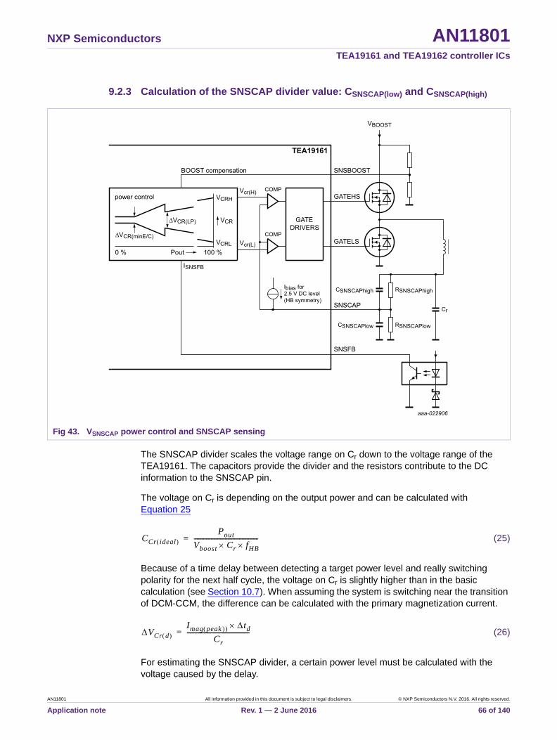
NXP Semiconductors AN11801TEA19161 and TEA19162 controller ICs
9.2.3 Calculation of the SNSCAP divider value: CSNSCAP(low) and CSNSCAP(high)
The SNSCAP divider scales the voltage range on Cr down to the voltage range of the TEA19161. The capacitors provide the divider and the resistors contribute to the DC information to the SNSCAP pin.
The voltage on Cr is depending on the output power and can be calculated with Equation 25
(25)
Because of a time delay between detecting a target power level and really switching polarity for the next half cycle, the voltage on Cr is slightly higher than in the basic calculation (see Section 10.7). When assuming the system is switching near the transition of DCM-CCM, the difference can be calculated with the primary magnetization current.
(26)
For estimating the SNSCAP divider, a certain power level must be calculated with the voltage caused by the delay.
Fig 43. VSNSCAP power control and SNSCAP sensing
CCr ideal Pout
Vboost Cr fHB-----------------------------------------=
VCr d Imag peak td
Cr----------------------------------------=
AN11801 All information provided in this document is subject to legal disclaimers. © NXP Semiconductors N.V. 2016. All rights reserved.
Application note Rev. 1 — 2 June 2016 66 of 140

NXP Semiconductors AN11801TEA19161 and TEA19162 controller ICs
(27)
VCr must match with the correct VSNSCAP.
For a 100 % power level at a nominal VSNSBOOST value (2.5 V), the voltage on the SNSCAP pin can be calculated with the formulas in Section 9.2.2.
(28)
The SNSCAP divider must match the 100 % power VCr with VSNSCAP = 0.96 V
Example for VCr:
(29)
According to this ratio, CSNSCAP(low) must be higher than the CSNSCAP(high).
(30)
9.2.4 Practical restrictions for SNSCAP divider
For correct functioning of the SNSCAP, there are a few practical restrictions to design the SNSCAP divider.
• Because the internal SNSCAP 2.5 V bias source can only source current, the divider must not cause the voltage on SNSCAP to exceed the DC-level of 2.5 V. The resistive divider (RSNSCAP(low) and RSNSCAP(high)) part must ensure that the DC-level is not exceeded.
• For the bias source of SNSCAP to operate correctly, the resistor value of the RSNSCAP(low) between the SNSCAP and GND pins must be higher than 15 k.
• During operation, the resistive part of the divider causes constant losses. It also causes constant losses during burst mode operation. To limit power losses, the total impedance must be high, e.g. RSNSCAP(low) + RSNSCAP(high) = 5 M.
After implementing the estimated values, check the result to the OPP reference level in the real application. The power level for triggering OPP must be correct. If it is not, the divider values must be corrected to achieve a good result.
When the SNSCAP divider is correct, the mode transition levels can be modified with specific settings as shown in Section 9.3.
9.2.5 SNSFB regulation
In the TEA19161, a special circuit is used to have a low current flowing in the feedback circuit continuously. The continuous low current helps to reach very low power consumption of the converter at no-load or low-load conditions.
VCr VCr ideal VCr d –=
VSNSCAP 21.67 V2.5 V---------------- 0.0075 100 0.96 V= =
VCr VCr ideal VCr d – 240 W390 V 47 nF 70 Hz--------------------------------------------------------- 1.3 A 450 ns
47 nF------------------------------------ 185 V=–= =
CSNSCAP low VCr VSNSCAP–
VSNSCAP-------------------------------------------- CSNSCAP high =
185 V 0.96 V–0.96 V
------------------------------------- CSNSCAP high 192 CSNSCAP high ==
AN11801 All information provided in this document is subject to legal disclaimers. © NXP Semiconductors N.V. 2016. All rights reserved.
Application note Rev. 1 — 2 June 2016 67 of 140
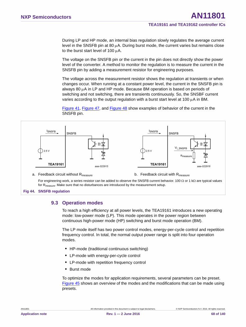
NXP Semiconductors AN11801TEA19161 and TEA19162 controller ICs
During LP and HP mode, an internal bias regulation slowly regulates the average current level in the SNSFB pin at 80 A. During burst mode, the current varies but remains close to the burst start level of 100 A.
The voltage on the SNSFB pin or the current in the pin does not directly show the power level of the converter. A method to monitor the regulation is to measure the current in the SNSFB pin by adding a measurement resistor for engineering purposes.
The voltage across the measurement resistor shows the regulation at transients or when changes occur. When running at a constant power level, the current in the SNSFB pin is always 80 A in LP and HP mode. Because BM operation is based on periods of switching and not switching, there are transients continuously. So, the SNSBF current varies according to the output regulation with a burst start level at 100 A in BM.
Figure 41, Figure 47, and Figure 48 show examples of behavior of the current in the SNSFB pin.
9.3 Operation modes
To reach a high efficiency at all power levels, the TEA19161 introduces a new operating mode: low-power mode (LP). This mode operates in the power region between continuous high-power mode (HP) switching and burst mode operation (BM).
The LP mode itself has two power control modes, energy-per-cycle control and repetition frequency control. In total, the normal output power range is split into four operation modes.
• HP-mode (traditional continuous switching)
• LP-mode with energy-per-cycle control
• LP-mode with repetition frequency control
• Burst mode
To optimize the modes for application requirements, several parameters can be preset. Figure 45 shows an overview of the modes and the modifications that can be made using presets.
a. Feedback circuit without Rmeasure b. Feedback circuit with Rmeasure
For engineering work, a series resistor can be added to observe the SNSFB current behavior. 100 or 1 k are typical values for Rmeasure. Make sure that no disturbances are introduced by the measurement setup.
Fig 44. SNSFB regulation
AN11801 All information provided in this document is subject to legal disclaimers. © NXP Semiconductors N.V. 2016. All rights reserved.
Application note Rev. 1 — 2 June 2016 68 of 140

NXP Semiconductors AN11801TEA19161 and TEA19162 controller ICs
9.3.1 High-Power (HP) mode
The HP-mode operates in continuous HBC switching with a 50 % duty cycle, which is similar to the traditional LLC operation via frequency control. The TEA1916, however, obtains the result by VSNSCAP control driving for voltage levels on the resonant capacitor instead of switching by time/frequency.
In all operation modes, the VSNSCAP level determines when the gate drive is switched off. When the correct VSNSCAP level for the required output power is reached, the gate drive is switched off.
The adaptive non-overlap function based on the HB end-of-slope detection switches on the gate drive.
9.3.2 Low-Power (LP) mode
The low-power mode is a kind of burst mode at high repetition frequency. In this mode, to provide a better conversion efficiency, the energy in each pulse is kept relatively high. During the not-switching period, the losses are low. To avoid audible noise, the repetition frequency of the complete LP cycle is higher than 23 kHz. The transition from HP-mode to LP-mode can be set at a certain power level with presets. To define the lower power part in the LP mode and the EC that it uses in BM, a Minimum Energy-per-Cycle (ECmin) can be set. When using an ECmin, the efficiency over the complete power range can be kept at a high level. A higher ECmin provides a higher efficiency in the low-power range. Consequently, the output ripple voltage becomes higher.
Fig 45. Operation modes and levels that can be modified with presets (in red)
AN11801 All information provided in this document is subject to legal disclaimers. © NXP Semiconductors N.V. 2016. All rights reserved.
Application note Rev. 1 — 2 June 2016 69 of 140
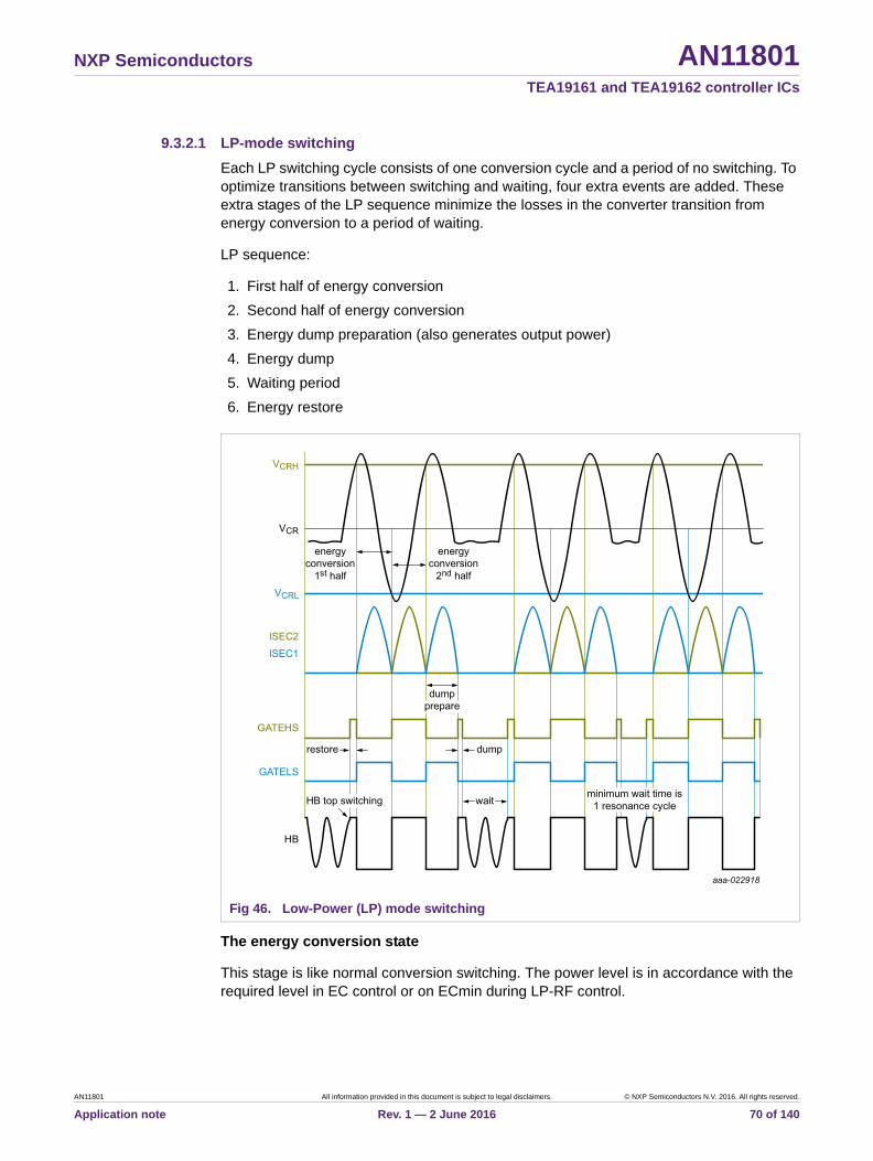
NXP Semiconductors AN11801TEA19161 and TEA19162 controller ICs
9.3.2.1 LP-mode switching
Each LP switching cycle consists of one conversion cycle and a period of no switching. To optimize transitions between switching and waiting, four extra events are added. These extra stages of the LP sequence minimize the losses in the converter transition from energy conversion to a period of waiting.
LP sequence:
1. First half of energy conversion
2. Second half of energy conversion
3. Energy dump preparation (also generates output power)
4. Energy dump
5. Waiting period
6. Energy restore
The energy conversion state
This stage is like normal conversion switching. The power level is in accordance with the required level in EC control or on ECmin during LP-RF control.
Fig 46. Low-Power (LP) mode switching
AN11801 All information provided in this document is subject to legal disclaimers. © NXP Semiconductors N.V. 2016. All rights reserved.
Application note Rev. 1 — 2 June 2016 70 of 140

NXP Semiconductors AN11801TEA19161 and TEA19162 controller ICs
Energy dump preparation
The controller holds the energy in the primary resonant capacitor at a level that leads to a minimum primary current flowing after switch-off. In this way, losses during the waiting stage are minimized.
This stage is very similar to the first half of the normal energy conversion state (GATELS on). Different is the switch-off level which is earlier than normal and leads to a slightly CCM switching on the output current.
Energy dump
The energy dump and the energy dump preparation cause the primary capacitor to hold energy at a level where a minimum primary current flows after switch off. The minimum current minimizes losses during the waiting stage. The energy dump consists of a short on-time for GATEHS.
Waiting period
The waiting period is the period of no switching where energy losses are minimal. This period reduces the average magnetization losses because there are no losses during the waiting period.
To minimize switching losses at the end of a waiting period, the restore stage starts when the voltage on the HB node is at the maximum level (top switching). The duration of the waiting period depends on the resonance behavior of the LLC. The minimum time of a waiting period is 1 resonance cycle. The duration can increase during the repetition frequency mode of LP, which leads to a waiting period of several resonance cycles.
Restore
To start the energy conversion after a waiting period, the resonant capacitor must be charged again to the correct VSNSCAP level. The charging is done using a shorter GATEHS switch-on/off action. Top switching on the GATEHS shows hard switching of the HB.
Hard switching in LP
Two switching events include hard switching:
• The start of the restore using top switching
• The end of the dump preparation because of output CCM switching
Top switching causes the TEA1916 to optimize the switching for the start restore state. To prevent some extra losses or voltage overshoot, the CCM switching requires some application attention on the secondary switch (diode or SR).
9.3.2.2 LP-mode with energy-per-cycle control
In the higher output power region of the LP mode, the energy control mechanism changes the power level via the amplitude of the 3 current pulses to the output.
AN11801 All information provided in this document is subject to legal disclaimers. © NXP Semiconductors N.V. 2016. All rights reserved.
Application note Rev. 1 — 2 June 2016 71 of 140
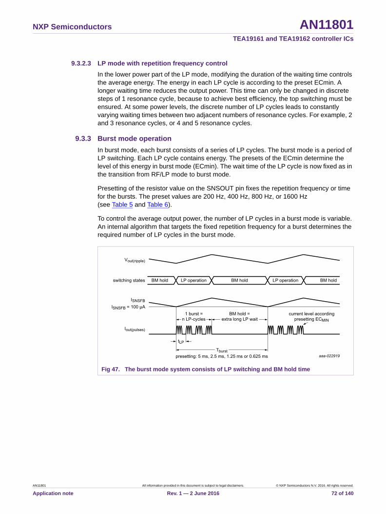
NXP Semiconductors AN11801TEA19161 and TEA19162 controller ICs
9.3.2.3 LP mode with repetition frequency control
In the lower power part of the LP mode, modifying the duration of the waiting time controls the average energy. The energy in each LP cycle is according to the preset ECmin. A longer waiting time reduces the output power. This time can only be changed in discrete steps of 1 resonance cycle, because to achieve best efficiency, the top switching must be ensured. At some power levels, the discrete number of LP cycles leads to constantly varying waiting times between two adjacent numbers of resonance cycles. For example, 2 and 3 resonance cycles, or 4 and 5 resonance cycles.
9.3.3 Burst mode operation
In burst mode, each burst consists of a series of LP cycles. The burst mode is a period of LP switching. Each LP cycle contains energy. The presets of the ECmin determine the level of this energy in burst mode (ECmin). The wait time of the LP cycle is now fixed as in the transition from RF/LP mode to burst mode.
Presetting of the resistor value on the SNSOUT pin fixes the repetition frequency or time for the bursts. The preset values are 200 Hz, 400 Hz, 800 Hz, or 1600 Hz (see Table 5 and Table 6).
To control the average output power, the number of LP cycles in a burst mode is variable. An internal algorithm that targets the fixed repetition frequency for a burst determines the required number of LP cycles in the burst mode.
Fig 47. The burst mode system consists of LP switching and BM hold time
AN11801 All information provided in this document is subject to legal disclaimers. © NXP Semiconductors N.V. 2016. All rights reserved.
Application note Rev. 1 — 2 June 2016 72 of 140
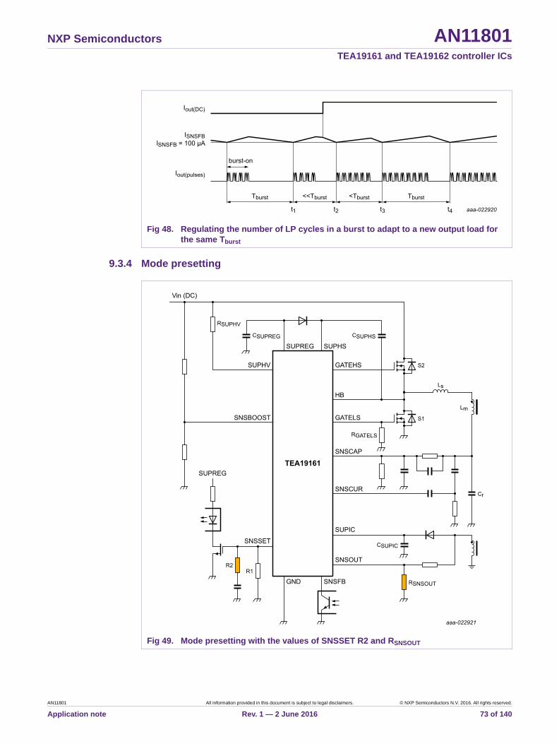
NXP Semiconductors AN11801TEA19161 and TEA19162 controller ICs
9.3.4 Mode presetting
Fig 48. Regulating the number of LP cycles in a burst to adapt to a new output load for the same Tburst
Fig 49. Mode presetting with the values of SNSSET R2 and RSNSOUT
AN11801 All information provided in this document is subject to legal disclaimers. © NXP Semiconductors N.V. 2016. All rights reserved.
Application note Rev. 1 — 2 June 2016 73 of 140

NXP Semiconductors AN11801TEA19161 and TEA19162 controller ICs
[1] Resistor RSNSOUT can set the burst repetition frequency: 4 values.
[2] HP to LP transition can be set by the R2 value on the SNSSET pin: 4 values.
[3] ECmin level or BM level can be set by the R2 value on SNSSET: 2 values depending on the value of RSNSOUT.
[1] Resistor RSNSOUT can set the burst repetition frequency: 4 values.
[2] HP to LP transition can be set by the R2 value on the SNSSET pin: 4 values.
[3] ECmin level or BM level can be set by the R2 value on SNSSET: 2 values depending on the value of RSNSOUT.
The values in Table 5 and Table 6 are including the additional shift due to a fixed internal time delay (150 ns) and a typical application delay (300 ns). With an external resistor and capacitor, these transition levels can be modified to a new table of values.
Table 5. Presetting for HP to LP transition and BM to LP transition
Burst repetition frequency[1] 200 Hz 400 Hz 800 Hz 1600 Hz
RSNSOUT 22 k 15 k 10 k 6.8 k
R2 (k) HP to LP transition(% of nominal power)[2]
BM to LP transition(% of nominal power)[3]
1 25 9 9 9 9
6.8 25 12 12 12 12
15 37.5 9 9 9 10
27 37.5 12 12 12 13
47 50 9 10 11 12
82 50 12 13 15 17
180 62.5 9 10 12 14
open 62.5 12 15 17.5 20
Table 6. Presetting for HP to LP transition and ECmin
Burst repetition frequency[1] 200 Hz 400 Hz 800 Hz 1600 Hz
RSNSOUT 22 k 15 k 10 k 6.8 k
R2 (k) HP to LP transition(% of nominal power)[2]
ECmin(% of nominal power)[3]
1 25 5 5 5 5
6.8 25 9 9 9 9
15 37.5 5 5 5 6
27 37.5 9 9 9 11
47 50 5 6 7 9
82 50 9 10 14 17
180 62.5 5 7 9 11
open 62.5 9 14 18 23
AN11801 All information provided in this document is subject to legal disclaimers. © NXP Semiconductors N.V. 2016. All rights reserved.
Application note Rev. 1 — 2 June 2016 74 of 140
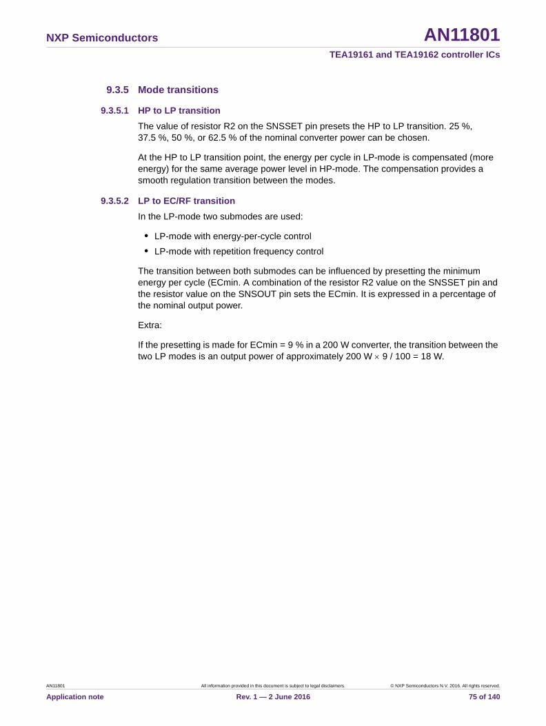
NXP Semiconductors AN11801TEA19161 and TEA19162 controller ICs
9.3.5 Mode transitions
9.3.5.1 HP to LP transition
The value of resistor R2 on the SNSSET pin presets the HP to LP transition. 25 %, 37.5 %, 50 %, or 62.5 % of the nominal converter power can be chosen.
At the HP to LP transition point, the energy per cycle in LP-mode is compensated (more energy) for the same average power level in HP-mode. The compensation provides a smooth regulation transition between the modes.
9.3.5.2 LP to EC/RF transition
In the LP-mode two submodes are used:
• LP-mode with energy-per-cycle control
• LP-mode with repetition frequency control
The transition between both submodes can be influenced by presetting the minimum energy per cycle (ECmin. A combination of the resistor R2 value on the SNSSET pin and the resistor value on the SNSOUT pin sets the ECmin. It is expressed in a percentage of the nominal output power.
Extra:
If the presetting is made for ECmin = 9 % in a 200 W converter, the transition between the two LP modes is an output power of approximately 200 W 9 / 100 = 18 W.
AN11801 All information provided in this document is subject to legal disclaimers. © NXP Semiconductors N.V. 2016. All rights reserved.
Application note Rev. 1 — 2 June 2016 75 of 140
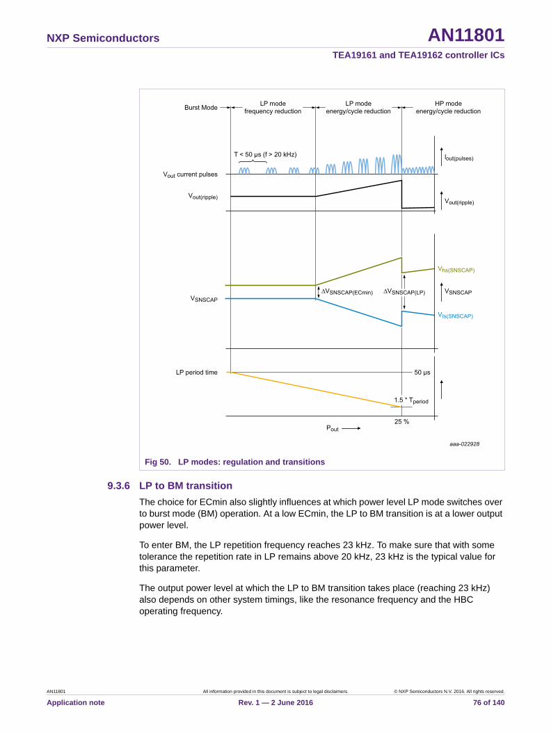
NXP Semiconductors AN11801TEA19161 and TEA19162 controller ICs
9.3.6 LP to BM transition
The choice for ECmin also slightly influences at which power level LP mode switches over to burst mode (BM) operation. At a low ECmin, the LP to BM transition is at a lower output power level.
To enter BM, the LP repetition frequency reaches 23 kHz. To make sure that with some tolerance the repetition rate in LP remains above 20 kHz, 23 kHz is the typical value for this parameter.
The output power level at which the LP to BM transition takes place (reaching 23 kHz) also depends on other system timings, like the resonance frequency and the HBC operating frequency.
Fig 50. LP modes: regulation and transitions
AN11801 All information provided in this document is subject to legal disclaimers. © NXP Semiconductors N.V. 2016. All rights reserved.
Application note Rev. 1 — 2 June 2016 76 of 140

NXP Semiconductors AN11801TEA19161 and TEA19162 controller ICs
9.3.7 Capacitive mode prevention using the SNSCUR pin
The primary current is measured accurately, cycle-by-cycle, for the internal switching logic. Two comparators of 100 mV above and below the 2.5 V bias voltage detect when the primary current is approaching capacitive mode operation. When this level is reached before VSNSCAP control switches off the gate, the capacitive mode prevention forces a switch-off. This switch-off prevents capacitive mode switching.
9.3.7.1 Practical application of CMR switching
Normally, design choices can prevent capacitive mode switching. But for some applications, performance parameters like system efficiency, can only be met when switching near capacitive mode is allowed when the input voltage Vboost decreases. The CMR function in the TEA19161 supports operation near capacitive mode by keeping the switching inductive at the border of the capacitive mode region. When the CMR is active, the output power is limited. The result is often a decrease of the voltage on the output.
9.3.7.2 Measuring the voltage on the SNSCUR pin
The voltage on the SNSCUR pin is difficult to measure because attaching a probe seriously disturbs operation. An internal bias source puts the input signal on a 2.5 V DC voltage level. A 2.2 nF capacitor connects the AC voltage that represents the resonant current signal to this pin. The AC voltage part can best be checked on the measurement resistor Rm.
a. Signals when running into capacitive mode operation
b. TEA1916 capacitive mode prevention. When 100 mV level is detected, GATEHS/LS is switched off.
Fig 51. Capacitive mode protection/prevention
AN11801 All information provided in this document is subject to legal disclaimers. © NXP Semiconductors N.V. 2016. All rights reserved.
Application note Rev. 1 — 2 June 2016 77 of 140
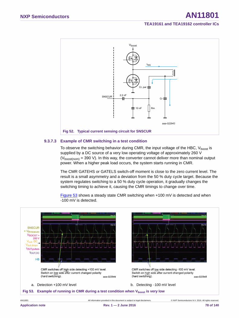
NXP Semiconductors AN11801TEA19161 and TEA19162 controller ICs
9.3.7.3 Example of CMR switching in a test condition
To observe the switching behavior during CMR, the input voltage of the HBC, Vboost is supplied by a DC source of a very low operating voltage of approximately 260 V (Vboost(nom) = 390 V). In this way, the converter cannot deliver more than nominal output power. When a higher peak load occurs, the system starts running in CMR.
The CMR GATEHS or GATELS switch-off moment is close to the zero current level. The result is a small asymmetry and a deviation from the 50 % duty cycle target. Because the system regulates switching to a 50 % duty cycle operation, it gradually changes the switching timing to achieve it, causing the CMR timings to change over time.
Figure 53 shows a steady state CMR switching when +100 mV is detected and when -100 mV is detected.
Fig 52. Typical current sensing circuit for SNSCUR
a. Detection +100 mV level b. Detecting 100 mV level
Fig 53. Example of running in CMR during a test condition when Vboost is very low
AN11801 All information provided in this document is subject to legal disclaimers. © NXP Semiconductors N.V. 2016. All rights reserved.
Application note Rev. 1 — 2 June 2016 78 of 140

NXP Semiconductors AN11801TEA19161 and TEA19162 controller ICs
To set the CMR to the best level in an application, the value of resistor Rm can be modified. The value of Rm also determines the OCP level. Normally, both levels are not very critical, a good value can be chosen. If a conflict remains, the option shown in Section 14.2.8 can be considered.
AN11801 All information provided in this document is subject to legal disclaimers. © NXP Semiconductors N.V. 2016. All rights reserved.
Application note Rev. 1 — 2 June 2016 79 of 140
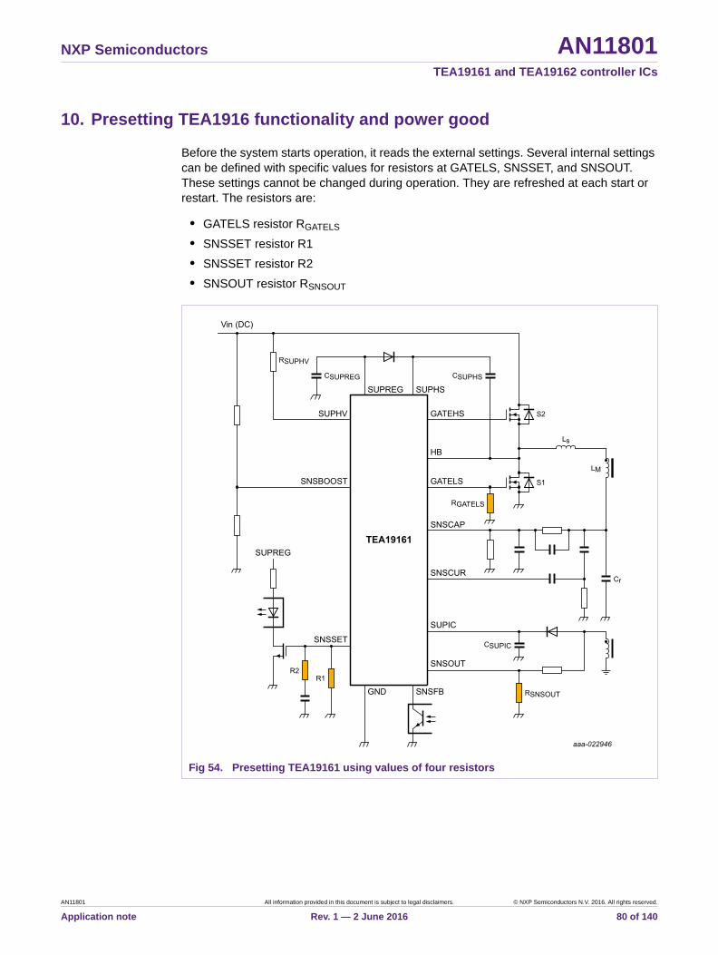
NXP Semiconductors AN11801TEA19161 and TEA19162 controller ICs
10. Presetting TEA1916 functionality and power good
Before the system starts operation, it reads the external settings. Several internal settings can be defined with specific values for resistors at GATELS, SNSSET, and SNSOUT. These settings cannot be changed during operation. They are refreshed at each start or restart. The resistors are:
• GATELS resistor RGATELS
• SNSSET resistor R1
• SNSSET resistor R2
• SNSOUT resistor RSNSOUT
Fig 54. Presetting TEA19161 using values of four resistors
AN11801 All information provided in this document is subject to legal disclaimers. © NXP Semiconductors N.V. 2016. All rights reserved.
Application note Rev. 1 — 2 June 2016 80 of 140

NXP Semiconductors AN11801TEA19161 and TEA19162 controller ICs
10.1 Setting the soft start power level (RGATELS)
To limit the power in each cycle at startup, the VSNSCAP control switching levels are given an offset.
During start-up, the slope compensation makes a sweep of 12 ms. The maximum start-up time is 12 ms. However, under normal conditions the start-up time is much shorter.
The amount of compensation that is used at start-up can be optimized with the value of
resistor RGATELS. The range of values for resistor RGATELS is: .
Any value within this range can be applied. The value is sampled in 255 steps accuracy which approaches an analog setting. At 100 k, the amount of energy in the first cycle is smallest and at 300 k it is largest.
This optimization function depends strongly on the application converter properties and behavior. So, when the behavior of the primary current and the output voltage increase is monitored, experimenting must determine the value. A typical value is 180 k.
During the start-up slope, functions that are also active during normal operation can influence the behavior.
• SNSBOOST pin: compensation for lower input voltage
• Symmetry regulation to keep the duty cycle close to 50 %
• SNSFB: start regulation when the nominal output voltage is reached
100 k RGATELS 300 k
a. RGATELS = 120 k b. RGATELS = 180 k c. RGATELS = 240 k
(1) HB (light blue signal)
(2) SNSCUR (VRmeasure; orange signal)
(3) GATELS (red signal)
(4) Vout (purple curve)
Fig 55. Start-up behavior at different values for resistor RGATELS
AN11801 All information provided in this document is subject to legal disclaimers. © NXP Semiconductors N.V. 2016. All rights reserved.
Application note Rev. 1 — 2 June 2016 81 of 140
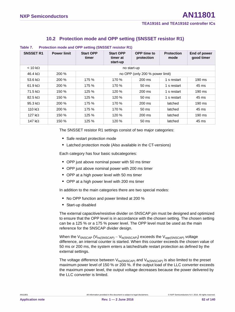
NXP Semiconductors AN11801TEA19161 and TEA19162 controller ICs
10.2 Protection mode and OPP setting (SNSSET resistor R1)
The SNSSET resistor R1 settings consist of two major categories:
• Safe restart protection mode
• Latched protection mode (Also available in the CT-versions)
Each category has four basic subcategories:
• OPP just above nominal power with 50 ms timer
• OPP just above nominal power with 200 ms timer
• OPP at a high power level with 50 ms timer
• OPP at a high power level with 200 ms timer
In addition to the main categories there are two special modes:
• No OPP function and power limited at 200 %
• Start-up disabled
The external capacitive/resistive divider on SNSCAP pin must be designed and optimized to ensure that the OPP level is in accordance with the chosen setting. The chosen setting can be a 125 % or a 175 % power level. The OPP level must be used as the main reference for the SNSCAP divider design.
When the VSNSCAP (Vhs(SNSCAP) Vls(SNSCAP)) exceeds the Vopp(SNSCAP) voltage difference, an internal counter is started. When this counter exceeds the chosen value of 50 ms or 200 ms, the system enters a latched/safe restart protection as defined by the external settings.
The voltage difference between Vhs(SNSCAP) and Vls(SNSCAP) is also limited to the preset maximum power level of 150 % or 200 %. If the output load of the LLC converter exceeds the maximum power level, the output voltage decreases because the power delivered by the LLC converter is limited.
Table 7. Protection mode and OPP setting (SNSSET resistor R1)
SNSSET R1 Power limit Start OPP timer
Start OPP timer at start-up
OPP time to protection
Protection mode
End of power good timer
< 10 k no start-up
46.4 k 200 % no OPP (only 200 % power limit)
53.6 k 200 % 175 % 170 % 200 ms 1 s restart 190 ms
61.9 k 200 % 175 % 170 % 50 ms 1 s restart 45 ms
71.5 k 150 % 125 % 120 % 200 ms 1 s restart 190 ms
82.5 k 150 % 125 % 120 % 50 ms 1 s restart 45 ms
95.3 k 200 % 175 % 170 % 200 ms latched 190 ms
110 k 200 % 175 % 170 % 50 ms latched 45 ms
127 k 150 % 125 % 120 % 200 ms latched 190 ms
147 k 150 % 125 % 120 % 50 ms latched 45 ms
AN11801 All information provided in this document is subject to legal disclaimers. © NXP Semiconductors N.V. 2016. All rights reserved.
Application note Rev. 1 — 2 June 2016 82 of 140
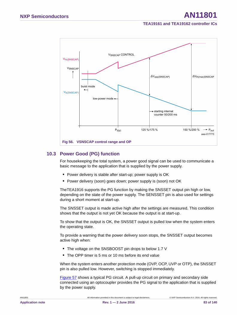
NXP Semiconductors AN11801TEA19161 and TEA19162 controller ICs
10.3 Power Good (PG) function
For housekeeping the total system, a power good signal can be used to communicate a basic message to the application that is supplied by the power supply.
• Power delivery is stable after start-up; power supply is OK
• Power delivery (soon) goes down; power supply is (soon) not OK
TheTEA1916 supports the PG function by making the SNSSET output pin high or low, depending on the state of the power supply. The SENSSET pin is also used for settings during a short moment at start-up.
The SNSSET output is made active high after the settings are measured. This condition shows that the output is not yet OK because the output is at start-up.
To show that the output is OK, the SNSSET output is pulled low when the system enters the operating state.
To provide a warning that the power delivery soon stops, the SNSSET output becomes active high when:
• The voltage on the SNSBOOST pin drops to below 1.7 V
• The OPP timer is 5 ms or 10 ms before its end value
When the system enters another protection mode (OVP, OCP, UVP or OTP), the SNSSET pin is also pulled low. However, switching is stopped immediately.
Figure 57 shows a typical PG circuit. A pull-up circuit on primary and secondary side connected using an optocoupler provides the PG signal to the application that is supplied by the power supply.
Fig 56. VSNSCAP control range and OP
AN11801 All information provided in this document is subject to legal disclaimers. © NXP Semiconductors N.V. 2016. All rights reserved.
Application note Rev. 1 — 2 June 2016 83 of 140

NXP Semiconductors AN11801TEA19161 and TEA19162 controller ICs
10.4 SNSSET R2: Power level for HP/LP transition
Presetting the HP/LP transition is done with the value of the R2 on SNSSET. The options possible are: 25 %, 37.5 %, 50 %, and 62.5 % of the nominal converter power.
At the HP/LP transition point, the energy per cycle in LP mode is compensated (higher) for the same average power level in HP mode. It provides a smooth regulation transition between the modes.
Two resistor values give the same transition level. The difference between the values is that they set a different minimum energy per cycle level for the LP mode (see Section 10.7).
The values in Table 8 include the additional shift due to a fixed internal time delay (150 ns) and a typical application delay (300 ns). These transition levels can be modified to a new table of values using an external resistor and capacitor.
a. Primary side b. Secondary side
Fig 57. Typical Power Good circuit
Table 8. Power level settings HP/LP transition
SNSSET R2 HP/LP transition level
1 k 25 %
6.8 k 25 %
15 k 37.5 %
27 k 37.5 %
47 k 50 %
82 k 50 %
180 k 62.5 %
open 62.5 %
AN11801 All information provided in this document is subject to legal disclaimers. © NXP Semiconductors N.V. 2016. All rights reserved.
Application note Rev. 1 — 2 June 2016 84 of 140

NXP Semiconductors AN11801TEA19161 and TEA19162 controller ICs
10.5 Capacitor value for the SNSSET pin
To measure the values for resistors R1 and R2 on the SNSSET pin, a capacitor is used in series with resistor R2. For reliable measurement, the value of this capacitor must be according to the table in Table 9.
10.6 RSNSOUT: Burst repetition frequency
The fixed burst repetition frequency can be set with the resistor value on the SNSOUT pin.
A lower repetition frequency reduces the risk of audible noise. However, it gives a higher output voltage ripple in burst mode. Determining the best resistor value on the SNSOUT pin, depends on the requirements for the power supply.
The minimum energy per cycle (ECmin) also influences the burst mode operation sequences. For each burst repetition frequency, there is a choice for two ECmin values that can be set with resistor R2 of the SNSSET pin.
The SNSOUT pin also includes a disable function. When the pin is actively pulled to GND, start-up of the HBC is disabled (RSNSOUT < 1.5 k).
Table 9. SNSSET capacitor (CSNSSET (nF)) value versus resistor values
1 6.8 15 27.0 47 82.0 180 open R2 (k)
46.4 33 33 33 33 33 22 12
53.6 33 33 33 33 33 22 12
61.9 33 33 33 33 33 22 12
71.5 33 33 33 33 22 22 12
82.5 33 33 33 22 22 22 12
95.3 33 33 22 22 22 12 12
110 22 22 22 22 22 12 12
127 22 22 22 22 12 12 12
147 22 22 22 12 12 12 12
R1 (k)
Table 10. Burst repetition frequency settings
RSNSOUT Burst repetition frequency
22 k 200 Hz
15 k 400 Hz
10 k 800 Hz
6.8 k 1600 Hz
< 1.5 k start-up disabled
AN11801 All information provided in this document is subject to legal disclaimers. © NXP Semiconductors N.V. 2016. All rights reserved.
Application note Rev. 1 — 2 June 2016 85 of 140

NXP Semiconductors AN11801TEA19161 and TEA19162 controller ICs
10.7 Burst mode transition level: SNSSET R2 and RSNSOUT
For each burst repetition frequency (RSNSOUT value) and HP-to-LP transition level, one of two BM-to-LP transition levels can be selected. These BM-to-LP transition levels can be set with resistor R2 of the SNSSET pin. Table 11 shows the possible combinations.
[1] Burst repetition frequency can be set with resistor RSNSOUT: 4 values.
[2] HP-to-LP transition can be set with resistor R2 on the SNSSET pin: 4 values.
[3] BM-to-LP transition can be set with resistor R2 on the SNSSET pin and with RSNSOUT.
The values in Table 11 include the additional shift due to a fixed internal time delay (150 ns) and a typical application delay (300 ns). These transition levels can be modified to a new table of values using an external resistor and capacitor.
10.7.1 Time delay VSNSCAP to HB transition
The mode transition levels are the expected levels in an application. When the SNSCAP divider scales the power correctly (according to the power supply requirements), the transition levels are given as a percentage of the nominal output power.
The level of transition depends on an internal SNSCAP target level and a time delay until the HB transition. The time delay includes:
• Time between the moment that SNSCAP reaches the target level (A) and the moment that the GATE switches off (B). This time is internally fixed: 150 ns.
• Time between the moment that the GATE switches off (B) and the moment that HB reaches half of its maximum value (C). This time depends on the application properties. In this document, 300 ns is assumed.
Table 11. HP-to-LP transition, BM-to-LP transition, and burst repetition frequency presets
Burst repetition frequency[1] 200 Hz 400 Hz 800 Hz 1600 Hz
RSNSOUT 22 k 15 k 10 k 6.8 k
SNSSET R2 HP LP (% of nominal power)[2] BM LP (% of nominal power[3]
1 k 25 9 9 9 9
6.8 k 25 12 12 12 12
15 k 37.5 9 9 9 10
27 k 37.5 12 12 12 13
47 k 50 9 10 11 12
82 k 50 12 13 15 17
180 k 62.5 9 10 12 14
open 62.5 12 15 17.5 20
AN11801 All information provided in this document is subject to legal disclaimers. © NXP Semiconductors N.V. 2016. All rights reserved.
Application note Rev. 1 — 2 June 2016 86 of 140

NXP Semiconductors AN11801TEA19161 and TEA19162 controller ICs
The time delay leads to a difference in power level between the control and reality. This difference can lead to a substantial difference in (mode transition) power levels. When the application-depending delay (B-C) is different from the 300 ns used in this document, the estimated power levels are different as well.
10.7.2 Accuracy of mode transition levels
Several component values and circuit properties contribute to the resulting mode transition level. Table 12 gives the list of contributions, including the specified or estimated example tolerances.
Fig 58. Time delay VSNSCAP to HB transition
Table 12. Specified and estimated example tolerances of contributing functions
Contributing item Tolerance Comment
resonant capacitor 10 % specification
capacitive divider SNSCAP 10 % specification
SNSCAP comparator levels 15 % specification
time delay 14 % estimation
SNSBOOST 3 % estimation; boost compensation
23 kHz timing spread 15 % estimation; BM transition only
total estimated spread: 30 root of squares(valid for normal distribution)
AN11801 All information provided in this document is subject to legal disclaimers. © NXP Semiconductors N.V. 2016. All rights reserved.
Application note Rev. 1 — 2 June 2016 87 of 140

NXP Semiconductors AN11801TEA19161 and TEA19162 controller ICs
Example:
When the nominal burst mode transition level is set for 1 A output current, the transition level is between 0.7 A and 1.3 A output current at normal distribution.
Using capacitor values with less spread can slightly improve the total tolerance.
10.8 Modify power levels for HP-to-LP and burst mode transition
Normally, the value resistor R2 of the SNSSET pin is chosen to set the mode transition levels. However, in some cases, the options in the table do not meet the requirements, e.g. when transitions must be set at a very low power level.
When a voltage offset is added to SNSCAP, the values in the Table 11 can be changed to meet the requirements. This offset has a similar effect as the time delay discussed in Section 10.7.1. The delay or offset shifts the total power range. However, it has a greater effect on the lower power region (near LP-to-BM transition) than on the higher power region (100 % level).
When the offset is added and the SNSCAP is modified to obtain the correct OPP level again, the transition table changes.
10.8.1 Adding an offset to the SNSCAP signal to modify (transition) power levels
The SNSCAP pin can be connected to the voltage on the auxiliary winding using resistor Roffset and capacitor Coffset. It adds a voltage to the SNSCAP signal for both polarities of the SNSCAP signal. The winding direction of the auxiliary winding determines whether an offset is added or subtracted.
This offset changes the power range defined by the SNSCAP divider.
Because it is important that the OPP level remains as required, the SNSCAP divider must be corrected.
When this offset circuit is added and the SNSCAP divider is modified, the values in the mode transition table are changed. Using this method, the user can create the table values that are best suited for the application to be designed.
The value of the auxiliary voltage and the value of Roffset determine the amount of offset on SNSCAP. Capacitor Coffset provides the AC coupling of the offset signal. The value of Coffset must allow correct timing for the function.
AN11801 All information provided in this document is subject to legal disclaimers. © NXP Semiconductors N.V. 2016. All rights reserved.
Application note Rev. 1 — 2 June 2016 88 of 140

NXP Semiconductors AN11801TEA19161 and TEA19162 controller ICs
10.8.2 Example of changed mode transition power levels
In most applications, the auxiliary winding is chosen to generate approximately 18 V to supply the SUPIC pin. Given this auxiliary voltage value, typical values for the offset components are:
• Roffset = 170 k
• Coffset = 120 pF
Using this offset in the TEA1916 240 W demo board results in a new SNSSET R2 table (see Table 13). Compare the values with the values in Table 11.
Fig 59. Adding an offset on SNSCAP to modify mode transition power levels
AN11801 All information provided in this document is subject to legal disclaimers. © NXP Semiconductors N.V. 2016. All rights reserved.
Application note Rev. 1 — 2 June 2016 89 of 140

NXP Semiconductors AN11801TEA19161 and TEA19162 controller ICs
[1] Roffset = 170 k; Coffset = 120 pF
Table 13. Mode transition power levels modified by adding an offset to SNSCAP[1]
Burst repetition frequency 200 Hz 400 Hz 800 Hz 1600 Hz
RSNSOUT 22 k 15 k 10 k 6.8 k
SNSSET R2 HP LP (% of nominal power) BM LP (% of nominal power
1 k 15 2.5 2.5 2.5 2.5
6.8 k 15 5 5 5 5
15 k 30 2.5 2.5 2.5 3
27 k 30 5 5 5 6
47 k 42.5 2.5 3 4 5
82 k 42.5 5 6 8 10
180 k 55 2.5 4 5 7
open 55 6 9 12 15
AN11801 All information provided in this document is subject to legal disclaimers. © NXP Semiconductors N.V. 2016. All rights reserved.
Application note Rev. 1 — 2 June 2016 90 of 140

NXP Semiconductors AN11801TEA19161 and TEA19162 controller ICs
11. Standby or no-load condition in burst mode operation
11.1 No-load power consumption
The currents that flow continuously in time mainly determine the power consumption during no-load operation. The energy used for power conversion in a burst is practically negligible because the bursts happen during a relatively short time. Figure 60 shows the main contributors to power consumption during no-load burst mode operation.
Converted power generates some currents. To obtain the power taken from the mains, these currents must be calculated using the conversion efficiency.
No load power consumption power in mW.
(1) Blue: Mains input filter = 4 mW
(2) Pink: Mains input measurement = 1 mW
(3) Light green: PFC output resistive divider = 10 mW
(4) Purple: Power in SNSCAP divider = 8 mW
(5) Green: Feedback circuit = 7 mW
(6) Orange: HBC output resistive divider = 4 mW
(7) Light blue: TEA1916 = 19 mW
Fig 60. Typical TEA1916 power consumption distribution in no-load condition
AN11801 All information provided in this document is subject to legal disclaimers. © NXP Semiconductors N.V. 2016. All rights reserved.
Application note Rev. 1 — 2 June 2016 91 of 140
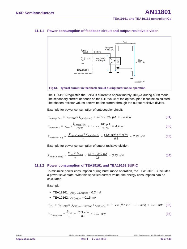
NXP Semiconductors AN11801TEA19161 and TEA19162 controller ICs
11.1.1 Power consumption of feedback circuit and output resistive divider
The TEA1916 regulates the SNSFB current to approximately 100 A during burst mode. The secondary current depends on the CTR value of the optocoupler. It can be calculated. The chosen resistor values determine the current through the output resistive divider.
Example for power consumption of optocoupler circuit:
(31)
(32)
(33)
Example for power consumption of output resistive divider:
(34)
11.1.2 Power consumption of TEA19161 and TEA19162 SUPIC
To minimize power consumption during burst mode operation, the TEA19161 IC includes a power save state. With this specified current value, the energy consumption can be calculated.
Example:
• TEA19161: ICC(burst)SUPIC = 0.7 mA
• TEA19162: ICC(ps)typ = 0.15 mA
(35)
(36)
Fig 61. Typical current in feedback circuit during burst mode operation
Popto prim VSUPIC Iopto prim 18 V 100 A 1.8 mW= = =
Popto sec Vout
Iopto prim
CTR------------------------ 12 V
100 A30 %
------------------ 4 mW= = =
Popto mains Popto prim Popto sec +
------------------------------------------------------------ 1.8 mW 4 mW+
0.8--------------------------------------------- 7.25 mW= = =
PRout mains Vout IRout
---------------------------- 12 V 250 A
0.8------------------------------------ 3.75 mW= = =
PICs VSUPIC ICC burst SUPIC ICC ps + 18 V 0.7 mA 0.15 mA+ 15.3 mW= = =
PICs mains PICs
---------- 15.3 mW
0.8---------------------- 19.1 mW= = =
AN11801 All information provided in this document is subject to legal disclaimers. © NXP Semiconductors N.V. 2016. All rights reserved.
Application note Rev. 1 — 2 June 2016 92 of 140
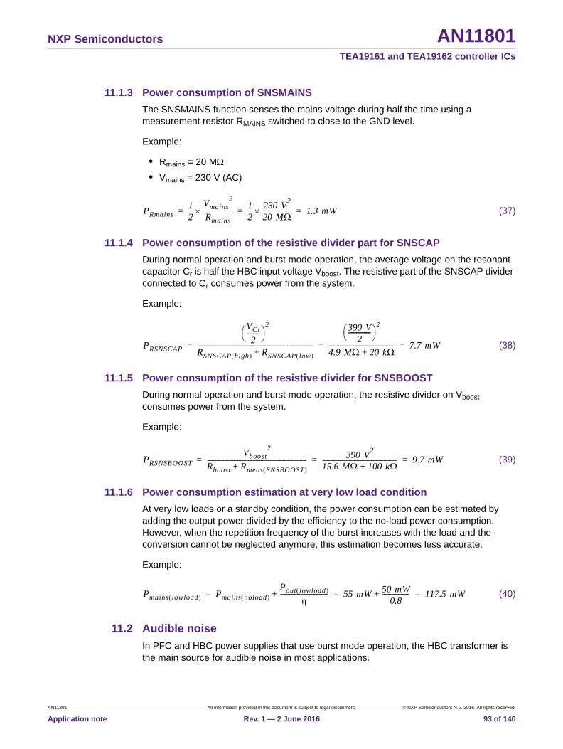
NXP Semiconductors AN11801TEA19161 and TEA19162 controller ICs
11.1.3 Power consumption of SNSMAINS
The SNSMAINS function senses the mains voltage during half the time using a measurement resistor RMAINS switched to close to the GND level.
Example:
• Rmains = 20 M
• Vmains = 230 V (AC)
(37)
11.1.4 Power consumption of the resistive divider part for SNSCAP
During normal operation and burst mode operation, the average voltage on the resonant capacitor Cr is half the HBC input voltage Vboost. The resistive part of the SNSCAP divider connected to Cr consumes power from the system.
Example:
(38)
11.1.5 Power consumption of the resistive divider for SNSBOOST
During normal operation and burst mode operation, the resistive divider on Vboost consumes power from the system.
Example:
(39)
11.1.6 Power consumption estimation at very low load condition
At very low loads or a standby condition, the power consumption can be estimated by adding the output power divided by the efficiency to the no-load power consumption. However, when the repetition frequency of the burst increases with the load and the conversion cannot be neglected anymore, this estimation becomes less accurate.
Example:
(40)
11.2 Audible noise
In PFC and HBC power supplies that use burst mode operation, the HBC transformer is the main source for audible noise in most applications.
PRmains12---
Vmains2
Rmains------------------ 1
2--- 230 V
2
20 M------------------ 1.3 mW= = =
PRSNSCAP
VCr
2--------
2
RSNSCAP high RSNSCAP low +-------------------------------------------------------------------------
390 V2
-------------- 2
4.9 M 20 k+----------------------------------------- 7.7 mW= = =
PRSNSBOOST
Vboost2
Rboost Rmeas SNSBOOST +--------------------------------------------------------------- 390 V
2
15.6 M 100 k+----------------------------------------------- 9.7 mW= = =
Pmains lowload Pmains noload Pout lowload
------------------------------+ 55 mW 50 mW
0.8-----------------+ 117.5 mW= = =
AN11801 All information provided in this document is subject to legal disclaimers. © NXP Semiconductors N.V. 2016. All rights reserved.
Application note Rev. 1 — 2 June 2016 93 of 140
NXP Semiconductors AN11801TEA19161 and TEA19162 controller ICs
11.2.1 Audible noise PFC converter
To minimize audible noise in the PFC burst mode and to prevent steep transients of PFC coil magnetization, a soft start and soft stop is included. The PFC burst mode operates independently from the HBC burst mode operation. At low output power, the HBC controller enables or disables PFC burst mode range. It activates the PFC burst mode in the lower output power part of the HBC burst mode range. The activation of the PFC burst mode is based on the duty cycle of the HBC burst.
11.2.2 Audible noise HBC converter
The converted energy in the HBC does not contribute to generate audible noise because the switching repetition is well above the audible frequency. However, in burst mode, the repetition frequency of the bursts is in the audible frequency range. The TEA19161 can be set to a steady repetition frequency of 1600 Hz, 800 Hz, 400 Hz, or 200 Hz. This operation can generate audible noise.
The LP mode enables the system to keep switching above the audible frequency down to low output power levels. The minimum energy per cycle (ECmin) can be set to modify the range of LP mode. A lower ECmin extends the LP range to lower power levels.
The main mechanism for producing noise is the interruption of magnetization current sequences (bursts), which leads to a mechanical force. The core of the resonant transformer is especially susceptible and starts acting like a loudspeaker. The noise amplitude is highest at the (mechanical) resonant frequency of the transformer. Normally, the resonant frequency of the transformer is a higher frequency than the burst repetition frequency. Harmonics of the burst repetition frequency produce the audible noise.
11.2.3 Measures in the coil and transformer construction
To reduce audible noise, measures can also be taken in the mechanical construction of the HBC transformer and PFC coil.
To reduce audible noise, a varnish is often put on the complete transformer. It is a commonly used method for systems that apply burst mode operation.
Because the resonance of the transformer is approximately 11 kHz, harmonics of 800 Hz produce most noise at the audio noise resonance frequency of the transformer.
Fig 62. Example of noise spectrum with 800 Hz burst repetition frequency
AN11801 All information provided in this document is subject to legal disclaimers. © NXP Semiconductors N.V. 2016. All rights reserved.
Application note Rev. 1 — 2 June 2016 94 of 140

NXP Semiconductors AN11801TEA19161 and TEA19162 controller ICs
If the windings itself produce noise, filling glue between the windings can be applied. Because this method makes the transformer production more difficult, it is not often used.
To reduce the noise from the core, softer air-gap material can be used. Because it requires non-standard air-gap material, this method is not often used.
AN11801 All information provided in this document is subject to legal disclaimers. © NXP Semiconductors N.V. 2016. All rights reserved.
Application note Rev. 1 — 2 June 2016 95 of 140

NXP Semiconductors AN11801TEA19161 and TEA19162 controller ICs
12. Practical system implementation topics
12.1 Questions and answers on settings options
How can the efficiency at low-load levels be increased?
• Increase the minimum energy per cycle (ECmin).
Example: SNSSET R2 = 82 k or R2 = open. For the same power levels, a higher current per cycle reduces number of switching cycles in time.
How can the output ripple voltage be reduced?
• Reduce the minimum energy per cycle (ECmin).
Example SNSSET R2 = 1 k or R2 = 15 k.
• Increase the burst mode repetition frequency.
Example: RSNSOUT = 10 k or 6.8 k. There are fewer cycles in each burst and a shorter time between bursts.
• Increase the value of the capacitors on the output voltage (not a setting).
Energy in each cycle or burst leads to less voltage increase and, when not switching, to less voltage decrease.
How to reduce audible noise?
• Reduce the burst mode repetition frequency.
Example: RSNSOUT = 15 k or 22 k. Higher harmonics generate the highest level of audible noise. When the basic harmonic is lower, the amplitude of the audible noise is less as well.
• Reduce minimum energy per cycle (ECmin).
Example: SNSSET R2 = 1 k or R2 = 15 k. The power range for burst mode decreases and LP mode (no audible noise) is extended.
• Mechanically improve the LLC transformer using a coating or flexible air gap material (not a setting).
Reduces the audible noise level that the transformer produces at a certain repetitive current operation.
How can the initial primary resonant current be reduced at start-up?
• Reduce the value of RGATELS.
Example RGATELS = 220 k 150 k. The switching starts with lower VSNSCAP levels (See Section 10.1).
The efficiency graph shows a lower efficiency in LP mode than just above the LP/HP transition in HP mode.
• The transition is probably near the highest efficiency region of the HP mode. Shift the LP/HP transition to a lower power level where it can improve the lower efficiency of the HP mode. Choose a lower transition level by decreasing the SNSSET R2 value. Example: SNSSET R2 = 27 k or R2 = 6.8 k.
AN11801 All information provided in this document is subject to legal disclaimers. © NXP Semiconductors N.V. 2016. All rights reserved.
Application note Rev. 1 — 2 June 2016 96 of 140
NXP Semiconductors AN11801TEA19161 and TEA19162 controller ICs
How can a transition to BM at a lower power level using settings be achieved?
• For modifying the presettable transition levels, an offset can be added using an additional resistor and capacitor to SNSCAP (see Section 10.8).
12.2 Questions and answers on debugging
My newly build power supply does not start up but probably immediately enters a protection.
Disable PFC operation as shown in Figure 63. First check if there is any HBC switching.
• If the HBC switches during a short time but soon stops, the most likely protections triggered are OCP, OVP or OPP. To see if the voltage on the SNSCUR and SNSOUT pins increases too much, this voltage can be measured. Another option is to temporarily disable the OCP function. Add two clamping diodes and disable the OVP function using a higher resistor value from the SNSOUT pin to the auxiliary winding signal.
The triggering of the OPP can be recognized by recognized by the typical time until protection, which is 50 ms or 200 ms, depending on the setting. A cause for OPP can be an error in the SNSCAP divider. If there is a wrong value in the SNSCAP function or the regulation by SNSFB is not working properly, not working at all, or unstable, it can cause false triggering of OCP, OVP, or OPP.
• If the HBC switches do not start switching, something may be wrong with the start-up conditions:
– The voltage on the SUPIC pin must have reached the start-up level
– The SUPREG pin must have reached the nominal voltage (11 V)
– The GATELS signal must be high; during the start-up, the GATELS resistor measurement must be seen (see Figure 55).
– The value measurements on the SNSSET and SNSOUT pins must be observed.
– The voltage on the SNSBOOST pin must be 2.3 V or higher.
– The SNSCUR and SNSCAP pins must have a bias voltage of 2.5 V.
• If the HBC switching is OK, enable the PFC and observe the start-up. First check if there are any PFC switching cycles.
• If the PFC does not start switching, something may be wrong on the start-up conditions:
– The voltage on the SUPIC pin must have reached the start-up level
– The PFCCOMP pin must have reached the initial bias voltage (3.5 V)
– The voltage on the SNSBOOST pin must reflect the rectified mains value on Vboost
• If the PFC starts switching because of GATEPFC pulses but the result is incorrect:
– The mains voltage is not detected and the X-capacitor discharge function is active (see Figure 36)
– An external OTP is wrongly detected because of a value error in the circuit.
– The regulation may be unstable. Observe the SNSBOOST voltage and the output voltage Vboost.
– The SNSBOOST voltage remains too low because output power is limited by OCP. Check the SNSCUR function and the measurement resistor.
AN11801 All information provided in this document is subject to legal disclaimers. © NXP Semiconductors N.V. 2016. All rights reserved.
Application note Rev. 1 — 2 June 2016 97 of 140
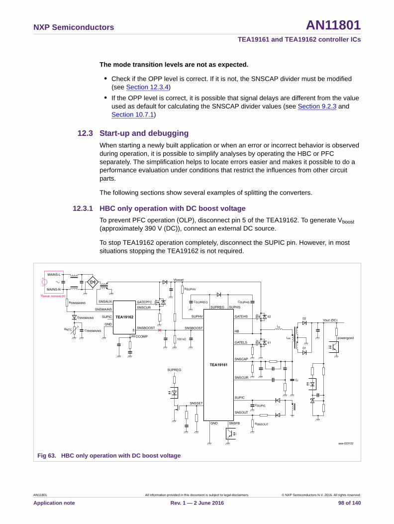
NXP Semiconductors AN11801TEA19161 and TEA19162 controller ICs
The mode transition levels are not as expected.
• Check if the OPP level is correct. If it is not, the SNSCAP divider must be modified (see Section 12.3.4)
• If the OPP level is correct, it is possible that signal delays are different from the value used as default for calculating the SNSCAP divider values (see Section 9.2.3 and Section 10.7.1)
12.3 Start-up and debugging
When starting a newly built application or when an error or incorrect behavior is observed during operation, it is possible to simplify analyses by operating the HBC or PFC separately. The simplification helps to locate errors easier and makes it possible to do a performance evaluation under conditions that restrict the influences from other circuit parts.
The following sections show several examples of splitting the converters.
12.3.1 HBC only operation with DC boost voltage
To prevent PFC operation (OLP), disconnect pin 5 of the TEA19162. To generate Vboost (approximately 390 V (DC)), connect an external DC source.
To stop TEA19162 operation completely, disconnect the SUPIC pin. However, in most situations stopping the TEA19162 is not required.
Fig 63. HBC only operation with DC boost voltage
AN11801 All information provided in this document is subject to legal disclaimers. © NXP Semiconductors N.V. 2016. All rights reserved.
Application note Rev. 1 — 2 June 2016 98 of 140

NXP Semiconductors AN11801TEA19161 and TEA19162 controller ICs
In some cases, it can be helpful to increase or decrease the DC boost voltage gradually to observe the HBC behavior. In this case, an external voltage of 2.5 V can be applied on TEA19161 pin 16 (SNSBOOST) to enable operation at lower boost voltage. And an external source of 20 V can be connected to TEA19161 SUPIC pin1 to supply the IC for operation.
Fig 64. Observe the HBC behavior at variable Vboost voltages
AN11801 All information provided in this document is subject to legal disclaimers. © NXP Semiconductors N.V. 2016. All rights reserved.
Application note Rev. 1 — 2 June 2016 99 of 140
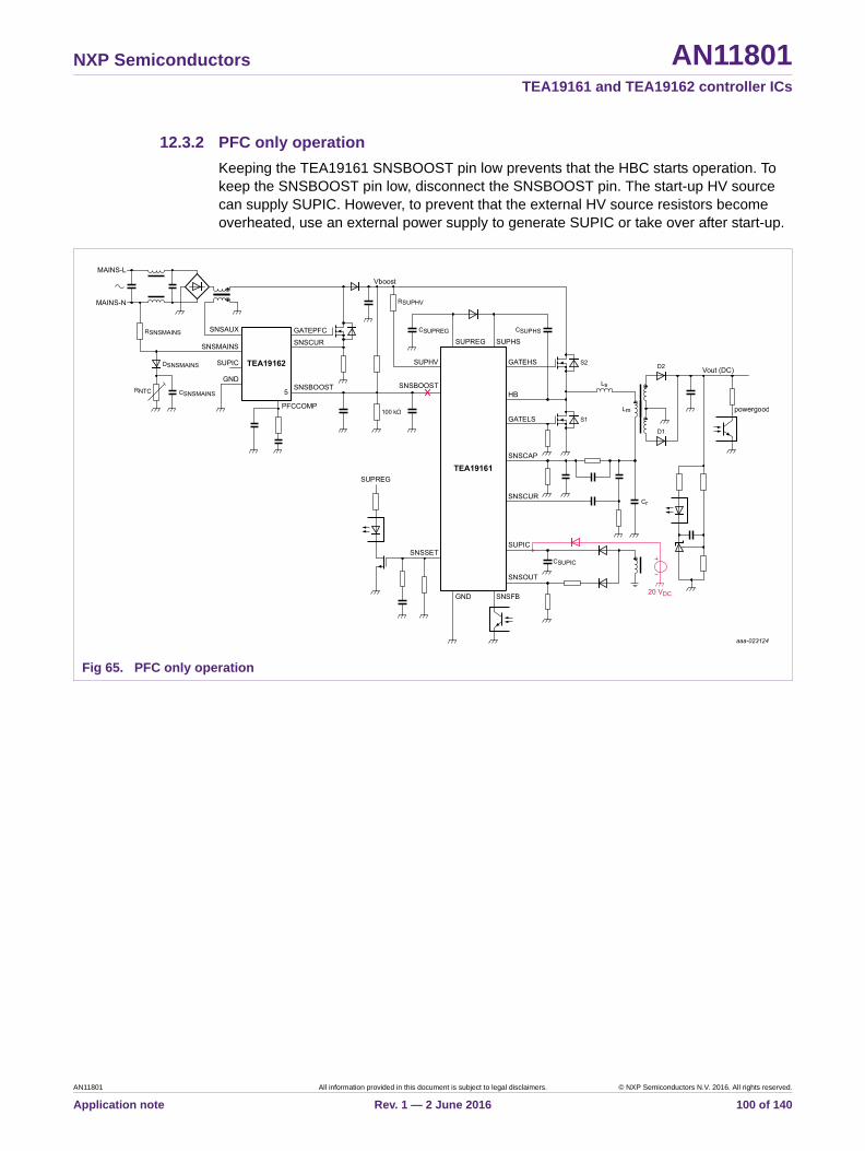
NXP Semiconductors AN11801TEA19161 and TEA19162 controller ICs
12.3.2 PFC only operation
Keeping the TEA19161 SNSBOOST pin low prevents that the HBC starts operation. To keep the SNSBOOST pin low, disconnect the SNSBOOST pin. The start-up HV source can supply SUPIC. However, to prevent that the external HV source resistors become overheated, use an external power supply to generate SUPIC or take over after start-up.
Fig 65. PFC only operation
AN11801 All information provided in this document is subject to legal disclaimers. © NXP Semiconductors N.V. 2016. All rights reserved.
Application note Rev. 1 — 2 June 2016 100 of 140

NXP Semiconductors AN11801TEA19161 and TEA19162 controller ICs
12.3.3 Splitting SNSBOOST for PFC and HBC operation
It is important to prevent that the SNSBOOST signal that is used by both controllers is disturbed. Proper layout of the PCB can be helpful (see Section 13.1).
If the cause of problems is expected to be on this signal, it can be debugged by temporarily splitting the connection into two parts, each with a separate resistive divider. To split the connection, temporarily add a second resistive divider. In this way, the behavior of each converter (PFC and HBC) can be checked separately.
Fig 66. HBC only operation with DC boost voltage and split SNSBOOST divider
AN11801 All information provided in this document is subject to legal disclaimers. © NXP Semiconductors N.V. 2016. All rights reserved.
Application note Rev. 1 — 2 June 2016 101 of 140

NXP Semiconductors AN11801TEA19161 and TEA19162 controller ICs
12.3.4 Checking the SNSCAP divider
After implementing the estimated SNSCAP divider values, it is important to check the result to the OPP reference level in the real application. There may be some application-specific deviation from the values in the estimation. If the power level for triggering OPP is not correct, the divider values must be corrected for a good result.
By programming an electronic load with a load step sequence, the system can be analyzed in the application. See the example in Figure 68 for checking 125 % OPP after 200 ms with safe restart.
Fig 67. HBC and PFC operation with split SNSBOOST divider
Fig 68. Testing the OPP level and timing
AN11801 All information provided in this document is subject to legal disclaimers. © NXP Semiconductors N.V. 2016. All rights reserved.
Application note Rev. 1 — 2 June 2016 102 of 140

NXP Semiconductors AN11801TEA19161 and TEA19162 controller ICs
When the measured OPP level is incorrect, the SNSCAP divider must be modified. In practice, modifying the SNSCAP divider can be done by making a small change to the CSNSCAP(low) value.
12.4 Load sweep for checking the mode transitions and the behavior
To observe the complete power range of the power supply, it is useful to apply a load sweep from no load to nominal load for a longer period (seconds). In this way, several properties and the behavior of the regulation and modes can be studied in one oscilloscope picture. Connecting a function generator signal to an analog input that drives the current load value enables this option for several electronic load devices.
Using this option, the following things can be checked:
• Regulation instability for certain load conditions
• Mode transitions at the expected or required power levels
• Output ripple voltage:
Is the output ripple voltage at the expected level? Or is it higher because of disturbances or instable operation at certain load conditions?
• Hysteresis at LP/HP transition:
Different transition levels between output power increasing and decreasing.
Fig 69. SNSCAP divider
AN11801 All information provided in this document is subject to legal disclaimers. © NXP Semiconductors N.V. 2016. All rights reserved.
Application note Rev. 1 — 2 June 2016 103 of 140

NXP Semiconductors AN11801TEA19161 and TEA19162 controller ICs
12.5 Converter with two output voltages
In some applications, two output voltages are required. Typical for TV applications is the requirement of a high output voltage for LED backlight power in addition to the lower (12 V) supply voltage.
Because it is not possible to regulate two output voltages, regulation issues occur sometimes during load step testing.
Fig 70. Load sweep to check the mode transitions and the behavior
AN11801 All information provided in this document is subject to legal disclaimers. © NXP Semiconductors N.V. 2016. All rights reserved.
Application note Rev. 1 — 2 June 2016 104 of 140

NXP Semiconductors AN11801TEA19161 and TEA19162 controller ICs
12.5.1 Regulation of two output voltages using shared feedback
To regulate two output voltages, the output voltage sensing can be split (see Figure 71a). The upper resistor of the voltage divider can be split into Rupper1 to Vout1 and Rupper2 to Vout2.
The contribution of each output can be chosen with the values of Rupper1 and Rupper2. One of the outputs is more important or critical than the other.
A disadvantage of this type of regulation is that the load of each output changes the output voltage of the other output.
Calculation example:
• Vout1 = 13 V
• Vout2 = 160 V
• Vref(error)amplifier = 2.5 V
• Rlower = 10 k
(41)
To find a solution, the value for resistor Rupper1 or Rupper2 must be slightly higher than but close to the value for a single output regulation.
a. Split feedback b. Capacitive coupling of outputs
Fig 71. Two methods of improving application behavior when using two output voltages
Ilower Itotal2.5 V10 k--------------- 0.25 mA= = =
AN11801 All information provided in this document is subject to legal disclaimers. © NXP Semiconductors N.V. 2016. All rights reserved.
Application note Rev. 1 — 2 June 2016 105 of 140
NXP Semiconductors AN11801TEA19161 and TEA19162 controller ICs
The Rupper1 value for a single output regulation becomes:
(42)
For split regulation, the value for Rupper1 must be higher, e.g. 51 k. If Rupper1 is 51 k, the current from the 13 V becomes:
(43)
The remaining current must flow from the 160 V output:
(44)
So, Rupper2 3.6 M.
In the examples above, the regulation contribution of each output is:
• Vout1:
• Vout2:
12.5.2 Output voltage coupling by connecting output capacitors
It is also possible to regulate the main output voltage only and to connect the other output voltage to the main output voltage with the output capacitor (see Figure 71b).
The current from a voltage change through the capacitor of the unregulated output also flows through the capacitor of the regulated output. Voltage variations on the unregulated output, e.g. during load steps, now have a similar effect on the regulated output. The feedback regulation for constant output voltage corrects variations and indirectly also regulates the unregulated output voltage.
The steady state behavior is not compensated because the coupling with the capacitors only shows the variations in current or voltage.
12.6 Checking limiting values in an application
Checking the condition on an IC-pin in a running application can be difficult because of disturbances. Normally, to see if a voltage on a pin is not exceeding the limiting value, an oscilloscope with a voltage probe is used. Because of switching disturbances, the measurement can easily show a voltage that is not on the pin but added by the probe. Or the connection of the probe adds energy to the application because of an antenna function. Both undesired effects show a higher voltage level than there really is on the pin.
To minimize errors in the measurement:
Rupper1
Vout1 Vref error amplifier– Itotal
------------------------------------------------------------------- 13 V 2.5 V– 0.25 mA
------------------------------------ 42 k= = =
IVout113 V 2.5 V–
51 k------------------------------------ 0.206 mA= =
IVout2 0.25 mA 0.206 mA– 0.044 mA= =
Rupper2
Vout2 Vref error amplifier– IVout2
------------------------------------------------------------------- 160 V 2.5 V– 0.044 mA
--------------------------------------- 3570 k= = =
100IVout1
Itotal-------------- 100
0.206 mA0.25 mA------------------------ 82.4 %= =
100IVout2
Itotal-------------- 100
0.044 mA0.25 mA------------------------ 17.6 %= =
AN11801 All information provided in this document is subject to legal disclaimers. © NXP Semiconductors N.V. 2016. All rights reserved.
Application note Rev. 1 — 2 June 2016 106 of 140
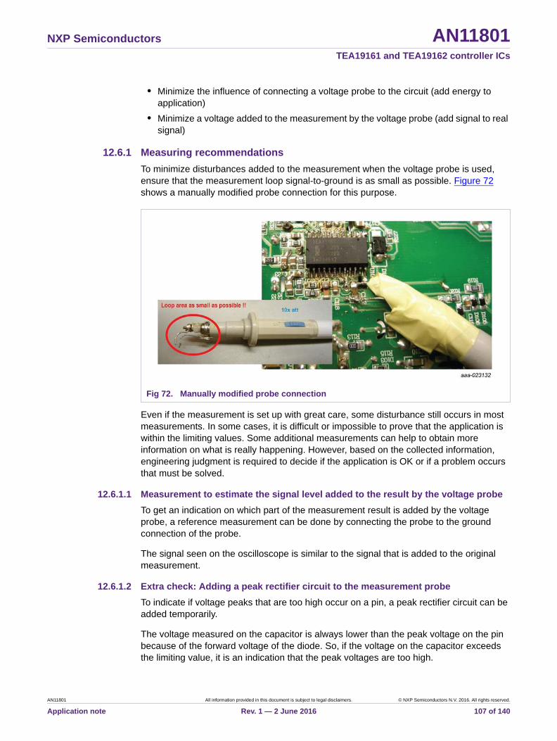
NXP Semiconductors AN11801TEA19161 and TEA19162 controller ICs
• Minimize the influence of connecting a voltage probe to the circuit (add energy to application)
• Minimize a voltage added to the measurement by the voltage probe (add signal to real signal)
12.6.1 Measuring recommendations
To minimize disturbances added to the measurement when the voltage probe is used, ensure that the measurement loop signal-to-ground is as small as possible. Figure 72 shows a manually modified probe connection for this purpose.
Even if the measurement is set up with great care, some disturbance still occurs in most measurements. In some cases, it is difficult or impossible to prove that the application is within the limiting values. Some additional measurements can help to obtain more information on what is really happening. However, based on the collected information, engineering judgment is required to decide if the application is OK or if a problem occurs that must be solved.
12.6.1.1 Measurement to estimate the signal level added to the result by the voltage probe
To get an indication on which part of the measurement result is added by the voltage probe, a reference measurement can be done by connecting the probe to the ground connection of the probe.
The signal seen on the oscilloscope is similar to the signal that is added to the original measurement.
12.6.1.2 Extra check: Adding a peak rectifier circuit to the measurement probe
To indicate if voltage peaks that are too high occur on a pin, a peak rectifier circuit can be added temporarily.
The voltage measured on the capacitor is always lower than the peak voltage on the pin because of the forward voltage of the diode. So, if the voltage on the capacitor exceeds the limiting value, it is an indication that the peak voltages are too high.
Fig 72. Manually modified probe connection
AN11801 All information provided in this document is subject to legal disclaimers. © NXP Semiconductors N.V. 2016. All rights reserved.
Application note Rev. 1 — 2 June 2016 107 of 140
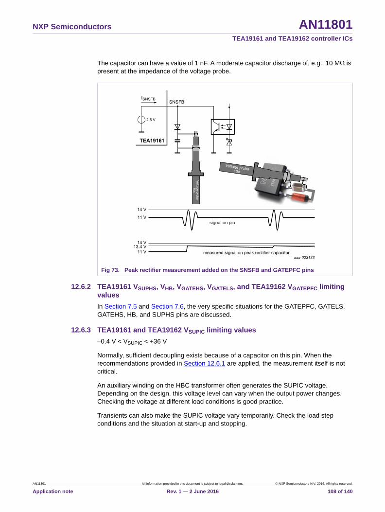
NXP Semiconductors AN11801TEA19161 and TEA19162 controller ICs
The capacitor can have a value of 1 nF. A moderate capacitor discharge of, e.g., 10 M is present at the impedance of the voltage probe.
12.6.2 TEA19161 VSUPHS, VHB, VGATEHS, VGATELS, and TEA19162 VGATEPFC limiting values
In Section 7.5 and Section 7.6, the very specific situations for the GATEPFC, GATELS, GATEHS, HB, and SUPHS pins are discussed.
12.6.3 TEA19161 and TEA19162 VSUPIC limiting values
0.4 V < VSUPIC < +36 V
Normally, sufficient decoupling exists because of a capacitor on this pin. When the recommendations provided in Section 12.6.1 are applied, the measurement itself is not critical.
An auxiliary winding on the HBC transformer often generates the SUPIC voltage. Depending on the design, this voltage level can vary when the output power changes. Checking the voltage at different load conditions is good practice.
Transients can also make the SUPIC voltage vary temporarily. Check the load step conditions and the situation at start-up and stopping.
Fig 73. Peak rectifier measurement added on the SNSFB and GATEPFC pins
AN11801 All information provided in this document is subject to legal disclaimers. © NXP Semiconductors N.V. 2016. All rights reserved.
Application note Rev. 1 — 2 June 2016 108 of 140

NXP Semiconductors AN11801TEA19161 and TEA19162 controller ICs
12.6.4 TEA19161 VSUPREG limiting values
0.4 V < VSUPREG < +12 V
Normally, sufficient decoupling exists because of a capacitor on this pin. When the recommendations provided in Section 12.6.1 are applied, the measurement itself is not critical.
The IC generates the SUPREG voltage. The SUPREG pin can only source current. It cannot actively sink current at the voltage regulator function. The IC uses this voltage to supply the MOSFET drivers. In some applications, an unintended voltage increase can occur because of currents through grounding tracks.
Normally, the SUPREG voltage is also used to create the bootstrap function for supplying the SUPHS pin using a diode. The SUPHS pin shows the rectified voltage on the SUPREG pin. When the voltage on the SUPREG pin has higher voltage peaks, the voltage on the SUPHS pin is higher than normal.
12.6.5 TEA19161 VSNSFB limiting values
0.4 V < VSNSFB < +12 V
Because the SNSFB function is current controlled at a relative low voltage with only an optocoupler connected, the risk of reaching limiting values is very small. When the recommendations provided in Section 12.6.1 are applied, the measurement itself is not critical.
12.6.6 TEA19161 VSNSOUT limiting values
0.4 V < VSNSOUT < +12 V
Normally, sufficient decoupling exists because of a capacitor on this pin. When the recommendations provided in Section 12.6.1 are applied, the measurement itself is not critical.
The signal on SNSOUT is alternating according to the converter switching. Much margin exists for the positive voltage. The negative voltage is closer to the limiting value. The voltage can be checked during regular operation to see if a grounding problem occurs. If the grounding problem does occur, a negative voltage that is too low can become an issue.
12.6.7 TEA19161 VSNSSET limiting values
0.4 V < VSNSSET < +12 V
The IC generates the voltage on this pin. The voltage is defined accurately. When the recommendations provided in Section 12.6.1 are applied, the measurement itself is not critical. No critical situations are expected on this pin.
12.6.8 TEA19161 VSNSCUR limiting values
0.4 V < VSNSCUR < +12 V
AN11801 All information provided in this document is subject to legal disclaimers. © NXP Semiconductors N.V. 2016. All rights reserved.
Application note Rev. 1 — 2 June 2016 109 of 140

NXP Semiconductors AN11801TEA19161 and TEA19162 controller ICs
The voltage on this pin is very difficult to measure because attaching a probe seriously disturbs operation. An internal bias source puts the input signal on a DC voltage level of 2.5 V. A capacitor connects the AC voltage that represents the resonant current signal to this pin. The AC voltage part can best be checked on the measurement resistor and not on the pin.
When the recommendations provided in Section 12.6.1 are applied, the measurement itself is not critical. The voltage reserve on the pin compared to the limiting values is substantial. So, the voltage is not critical.
If measurement on the pin is required, use the rectifier method to observe the behavior.
12.6.9 TEA19161 VSNSCAP limiting values
0.4 V < VSNSCAP < +12 V
Normally, sufficient decoupling exists because of the CSNSCAP(low) capacitor on this pin. When the recommendations provided in Section 12.6.1 are applied, the measurement itself is not critical.
An internal bias source puts the input signal on a DC voltage level of 2.5 V. The voltage reserve on the pin compared to the limiting values is substantial. So, the voltage is not critical.
12.6.10 TEA19161 VSNSBOOST limiting values
0.4 V < VSNSBOOST < +12 V
Normally, sufficient decoupling exists because of the CSNSCAP(low) capacitor on this pin. When the recommendations provided in Section 12.6.1 are applied, the measurement itself is not critical.
If the PFC loop regulation stability is critical or the track connecting the TEA19161 with the TEA19162 is long, a measurement with a voltage probe can disturb the PFC operation. Because the PFC regulation is at 2.5 V and a capacitor of several nanofarads is connected, this pin is not critical concerning limiting values.
12.6.11 TEA19162 VSNSMAINS limiting values
0.4 V < VSNSBOOST < +12 V
Because SNSMAINS is connected to the mains voltage with a high impedance (typical 20 M), connecting a voltage probe influences the mains measurements a little. This impact is not directly a problem because operation normally continues in a similar way. The measurement can be made in alignment with the recommendations mentioned in Section 12.6.1.
12.6.12 TEA19162 VPFCCOMP limiting values
0.4 V < VSNSBOOST < +12 V
Normally, sufficient decoupling occurs because of the filter on the PFCCOMP pin. When the recommendations provided in Section 12.6.1 are applied, the measurement itself is not critical.
The IC generates the signal on this pin. So, it is not critical concerning limiting values.
AN11801 All information provided in this document is subject to legal disclaimers. © NXP Semiconductors N.V. 2016. All rights reserved.
Application note Rev. 1 — 2 June 2016 110 of 140

NXP Semiconductors AN11801TEA19161 and TEA19162 controller ICs
12.6.13 TEA19162 VSNSAUX limiting values
0.4 V < VSNSBOOST < +12 V
The measurement can be made in alignment with the recommendations in Section 12.6.1. An auxiliary winding on the PFC coil generated the voltage on this pin. Because only a few turns normally make this winding, the voltage signal can be close to the limiting values. Although the allowed voltage range is wide, the measurement itself can be difficult because of the PFC switching, which can distort the measurement result.
12.6.14 TEA19162 VSNSCUR limiting values
0.4 V < VSNSBOOST < +12 V
The measurement can be made in alignment with the recommendations in Section 12.6.1. The measurement itself can be difficult because of the PFC switching, which can distort the measurement result.
Although the measured signal for this pin comes from a very low impedance resistor, voltage spikes can occur because of the PFC MOSFET switching. Also, if there is a PCB layout grounding problem, high converter currents through the ground tracks can add a signal to the SNSCUR pin.
The most critical situation is at a low mains voltage and a high output power.
12.6.15 TEA19162 VSNSBOOST limiting values
0.4 V < VSNSBOOST < +12 V
Normally, sufficient decoupling exists because of a capacitor on this pin. When the recommendations provided in Section 12.6.1 are applied, the measurement itself is not critical.
If the loop regulation is critical, a measurement with a voltage probe can disturb operation. Because regulation is at 2.5 V and a capacitor of several nanofarads is connected this pin is not critical concerning limiting values.
AN11801 All information provided in this document is subject to legal disclaimers. © NXP Semiconductors N.V. 2016. All rights reserved.
Application note Rev. 1 — 2 June 2016 111 of 140

NXP Semiconductors AN11801TEA19161 and TEA19162 controller ICs
13. Important PCB layout design rules
13.1 Short SNSBOOST track length
To avoid mutual disturbance because of converter switching, the TEA19161 (HBC) and TEA19162 (PFC) must have a separate PCB layout structure. A greater distance between the converters can help. However, the SNSBOOST track that connects both controllers for communication and boost voltage sensing carries a high impedance divider signal that is sensitive to disturbance.
To avoid disturbances:
• To minimize the length of the SNSBOOST track between the two ICs, the TEA19161 and TEA19162 ICs must be placed relatively close to each other.
• The SNSBOOST resistive divider position must be optimized for PFC regulation loop performance.
• Two disturbance filtering capacitors from SNSBOOST to GND must be present. A higher value (typical between 1 nF and 4.7 nF) near the TEA19162 (PFC) and a lower value (typical 680 pF) near the TEA19161 (HBC).
Yellow marked area: SNSBOOST connection.
Red marked area:TEA19161 and TEA19162 ICs
Fig 74. Short SNSBOOST track between TEA19161 and TEA19162
AN11801 All information provided in this document is subject to legal disclaimers. © NXP Semiconductors N.V. 2016. All rights reserved.
Application note Rev. 1 — 2 June 2016 112 of 140

NXP Semiconductors AN11801TEA19161 and TEA19162 controller ICs
13.2 TEA19161: Shielding the SNSFB track
Because the SNSFB function works on small current levels to minimize energy consumption at no load, this signal is more sensitive to disturbances.
The main reason for disturbance that can make regulation unstable is capacitive coupling to converter switching tracks (HB or PFC-drain). To avoid disturbance in SNSFB:
• The SNSFB track must be placed relatively far from the power part of the converters (HBC and PFC).
• To shield the SNSFB track, put grounded tracks alongside it (and a ground plane in case of double-sided copper design)
• The SNSFB track does not have to be short. To obtain a greater distance to HB, a longer track is required.
Yellow marked area: SNSFB
Blue marked area: Shielding GND
Green marking rectangle: SNSFB layout area
Green arrows: Showing that SNSFB is placed far from HBC and PFC converter switching
Red marked area: Shows a compact TL431 circuit design
Fig 75. SNSFB: A longer but shielded track far from the converter switching
AN11801 All information provided in this document is subject to legal disclaimers. © NXP Semiconductors N.V. 2016. All rights reserved.
Application note Rev. 1 — 2 June 2016 113 of 140
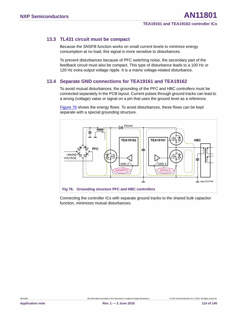
NXP Semiconductors AN11801TEA19161 and TEA19162 controller ICs
13.3 TL431 circuit must be compact
Because the SNSFB function works on small current levels to minimize energy consumption at no load, this signal is more sensitive to disturbances.
To prevent disturbances because of PFC switching noise, the secondary part of the feedback circuit must also be compact. This type of disturbance leads to a 100 Hz or 120 Hz extra output voltage ripple. It is a mains voltage-related disturbance.
13.4 Separate GND connections for TEA19161 and TEA19162
To avoid mutual disturbances, the grounding of the PFC and HBC controllers must be connected separately in the PCB layout. Current pulses through ground tracks can lead to a wrong (voltage) value or signal on a pin that uses the ground level as a reference.
Figure 76 shows the energy flows. To avoid disturbances, these flows can be kept separate with a special grounding structure.
Connecting the controller ICs with separate ground tracks to the shared bulk capacitor function, minimizes mutual disturbances.
Fig 76. Grounding structure PFC and HBC controllers
AN11801 All information provided in this document is subject to legal disclaimers. © NXP Semiconductors N.V. 2016. All rights reserved.
Application note Rev. 1 — 2 June 2016 114 of 140
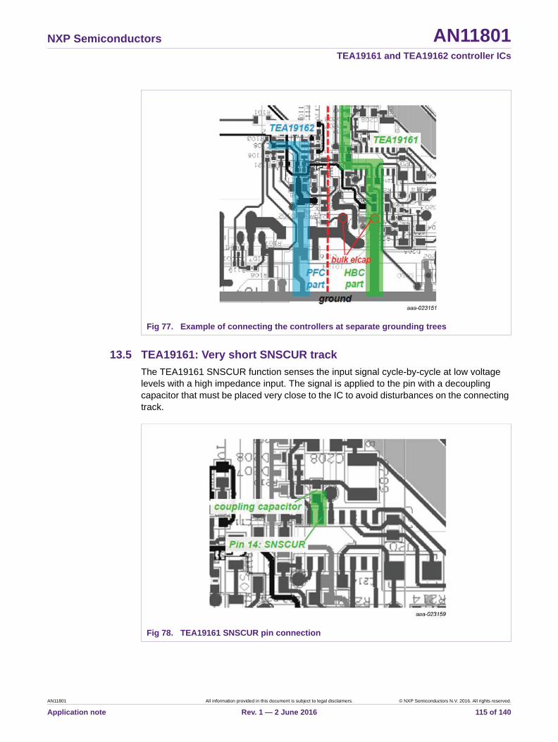
NXP Semiconductors AN11801TEA19161 and TEA19162 controller ICs
13.5 TEA19161: Very short SNSCUR track
The TEA19161 SNSCUR function senses the input signal cycle-by-cycle at low voltage levels with a high impedance input. The signal is applied to the pin with a decoupling capacitor that must be placed very close to the IC to avoid disturbances on the connecting track.
Fig 77. Example of connecting the controllers at separate grounding trees
Fig 78. TEA19161 SNSCUR pin connection
AN11801 All information provided in this document is subject to legal disclaimers. © NXP Semiconductors N.V. 2016. All rights reserved.
Application note Rev. 1 — 2 June 2016 115 of 140

NXP Semiconductors AN11801TEA19161 and TEA19162 controller ICs
13.6 TEA19162: placing of SNSMAINS mains sensing resistors
To save power, the TEA19162 PFC controller SNSMAINS mains sensing function uses low current levels. To avoid disturbances, the mains sensing resistors must be placed close to the IC.
Fig 79. SNSMAINS mains sensing resistors placed close to the TEA19162
AN11801 All information provided in this document is subject to legal disclaimers. © NXP Semiconductors N.V. 2016. All rights reserved.
Application note Rev. 1 — 2 June 2016 116 of 140
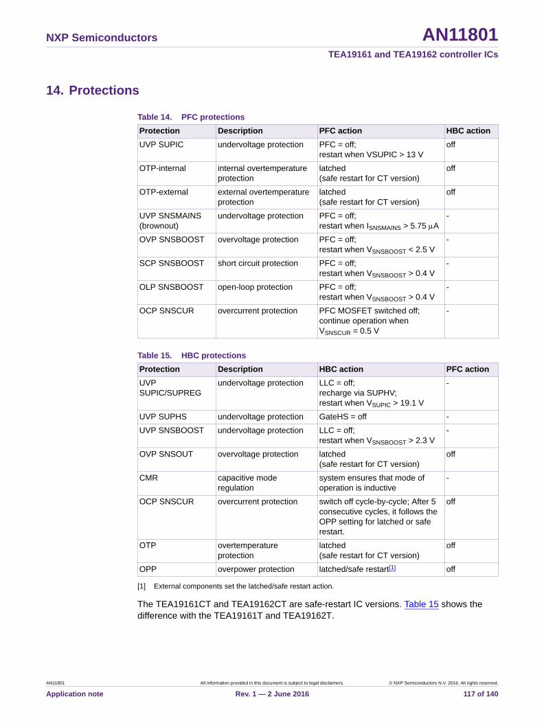
NXP Semiconductors AN11801TEA19161 and TEA19162 controller ICs
14. Protections
[1] External components set the latched/safe restart action.
The TEA19161CT and TEA19162CT are safe-restart IC versions. Table 15 shows the difference with the TEA19161T and TEA19162T.
Table 14. PFC protections
Protection Description PFC action HBC action
UVP SUPIC undervoltage protection PFC = off;restart when VSUPIC > 13 V
off
OTP-internal internal overtemperature protection
latched(safe restart for CT version)
off
OTP-external external overtemperature protection
latched(safe restart for CT version)
off
UVP SNSMAINS (brownout)
undervoltage protection PFC = off;restart when ISNSMAINS > 5.75 A
-
OVP SNSBOOST overvoltage protection PFC = off;restart when VSNSBOOST < 2.5 V
-
SCP SNSBOOST short circuit protection PFC = off;restart when VSNSBOOST > 0.4 V
-
OLP SNSBOOST open-loop protection PFC = off;restart when VSNSBOOST > 0.4 V
-
OCP SNSCUR overcurrent protection PFC MOSFET switched off; continue operation when VSNSCUR = 0.5 V
-
Table 15. HBC protections
Protection Description HBC action PFC action
UVP SUPIC/SUPREG
undervoltage protection LLC = off;recharge via SUPHV;restart when VSUPIC > 19.1 V
-
UVP SUPHS undervoltage protection GateHS = off -
UVP SNSBOOST undervoltage protection LLC = off;restart when VSNSBOOST > 2.3 V
-
OVP SNSOUT overvoltage protection latched(safe restart for CT version)
off
CMR capacitive mode regulation
system ensures that mode of operation is inductive
-
OCP SNSCUR overcurrent protection switch off cycle-by-cycle; After 5 consecutive cycles, it follows the OPP setting for latched or safe restart.
off
OTP overtemperature protection
latched(safe restart for CT version)
off
OPP overpower protection latched/safe restart[1] off
AN11801 All information provided in this document is subject to legal disclaimers. © NXP Semiconductors N.V. 2016. All rights reserved.
Application note Rev. 1 — 2 June 2016 117 of 140

NXP Semiconductors AN11801TEA19161 and TEA19162 controller ICs
14.1 PFC protections
14.1.1 UVP SUPIC
When the voltage on the SUPIC pin drops to below 9 V, the IC stops operation. A system reset is activated at 3.5 V.
When the SUPIC voltage drops to 14 V during the non-switching period in burst mode, the TEA19161 HV source is activated. It regulates the SUPIC voltage with a hysteresis of 0.9 V above 14 V, which avoids that the system stops during a long non-switching period (see Section 6).
14.1.2 OverTemperature Protection (OTP)
The TEA19162 provides two OTP protections, an internal and external OTP. Both protections provide a latched protection until the decreasing of the SUPIC or SNSMAINS voltages resets the latched condition. For the CT versions, the OTP protections trigger a safe restart.
Pulling up the voltage on the SNSBOOST pin to above 2 V during engineering or production testing can also reset a latched protection.
14.1.2.1 Internal OTP
The IC contains an internal temperature protection. When the internal temperature exceeds 150 C, the PFC stops operation. It also disables the HBC operation by pulling down the SNSBOOST voltage.
14.1.2.2 External OTP
The SNSMAINS pin combines two functions. The mains voltage sensing and the sensing of an external NTC for detecting an OTP. The functions are alternatingly active in time. Each function is active during a half-mains voltage cycle.
During the period of OTP sensing a current of 200 A from an internal source flows from the pin through the external diode and NTC to ground. The resulting voltage on pin is measured. When the voltage on the pin is below 2 V at four consecutive measuring cycles, the OTP protection is activated.
14.1.2.3 Not using the external OTP function
When no external OTP function is required, the external OTP components can be omitted.
AN11801 All information provided in this document is subject to legal disclaimers. © NXP Semiconductors N.V. 2016. All rights reserved.
Application note Rev. 1 — 2 June 2016 118 of 140

NXP Semiconductors AN11801TEA19161 and TEA19162 controller ICs
14.1.3 UVP SNSMAINS (brownout)
At an SNSMAINS peak current level of 5.75 A, the PFC start-up is enabled (brownin). At 5 A, the operation is disabled (brownout; see Section 8.3).
14.1.4 OVP SNSBOOST
The overvoltage protection circuit prevents output overvoltage during load steps and mains transients. When the voltage on the SNSBOOST pin exceeds 2.63 V for a period longer than 100 s, the switching is stopped. When the voltage drops to below 2.53 V, the switching resumes with a soft start.
14.1.5 SCP and OLP SNSBOOST
The PFC does not start switching until the voltage on the SNSBOOST pin exceeds Vstart(scp) (0.5 V). This function protects against a short circuit and an open-loop condition on SNSBOOST.
14.1.6 OCP SNSCUR
Sensing the voltage across an external sense resistor in series with the source of the PFC MOSFET limits the maximum PFC peak current cycle-by-cycle. The voltage is measured via the SNSCUR pin. It is limited to 0.5 V. When the voltage on the SNSCUR pin reaches 0.5 V, the MOSFET is switched off (see Section 8.17).
14.2 HBC protections
14.2.1 UVP SUPIC and SUPREG
When the SUPIC voltage has reached the start level of 19.1 V, the IC operation is enabled. If the HV source supplies the IC, the SUPIC voltage is regulated with a hysteresis of 0.7 V. When the SUPIC voltage drops to below 13.2 V, the converter stops operating. When the SUPIC voltage reaches 3.5 V, a system reset is activated.
When the SUPIC voltage drops to 14 V during the non-switching period in burst mode, the HV source is activated. It regulates the SUPIC voltage with a hysteresis of 0.9 V above 14 V, which avoids that the system stops during a long non-switching period.
a. SNSMAINS with external OTP b. SNSMAINS without external OTP
Fig 80. SNSMAINS with and without OTP function using external NTC
AN11801 All information provided in this document is subject to legal disclaimers. © NXP Semiconductors N.V. 2016. All rights reserved.
Application note Rev. 1 — 2 June 2016 119 of 140

NXP Semiconductors AN11801TEA19161 and TEA19162 controller ICs
The series stabilizer for the SUPREG pin is charged along with the SUPIC pin. To enable HBC operation, the SUPREG voltage must reach the 11 V regulation level. When SUPREG voltage drops below 9 V, the IC stops operating (see Section 6).
14.2.2 UVP SUPHS
When the voltage across capacitor CSUPHS (VSUPHS VHB) drops to below 7 V, the driver stops operation to prevent unreliable switching (see Section 6.6).
14.2.3 UVP SNSBOOST
When the voltage on the SNSBOOST pin drops to below 1.6 V, the HBC stops switching when the low-side MOSFET is on. When the SNSBOOST voltage exceeds the start level of 2.3 V, the HBC start/restarts (see Section 9.1).
14.2.4 OVP on the SNSOUT pin
SNSOUT provides two main functions:
• Setting the burst mode repetition frequency
• OVP function at 3.5 V
The resistor value from SNSOUT to ground (R2) must be correct for the burst mode repetition frequency setting. The value of R1 can be used to make the correct resistive divider for sensing the peak voltage from the auxiliary winding that represents the HBC output voltage (Vout). When this voltage exceeds 3.5 V during the internal time delay, the system stops switching and enters a latched protection or a safe restart sequence.
Fig 81. SNSOUT OVP function
AN11801 All information provided in this document is subject to legal disclaimers. © NXP Semiconductors N.V. 2016. All rights reserved.
Application note Rev. 1 — 2 June 2016 120 of 140

NXP Semiconductors AN11801TEA19161 and TEA19162 controller ICs
14.2.4.1 Time delay until protection
To prevent false triggering by short events or disturbances, the OVP function includes a time delay. An internal counter monitors the number of cycles that show a higher SNSOUT voltage. When the number of pulses reaches approximately 11, the protection is activated (latched or safe-restart). Because of the internal sampling method that uses a digital-to-analog converter for several functions by time multiplexing, there can be an error of 1 cycle for the time delay. So, the delay can be 10, 11, or 12 cycles.
To prevent a short delay time for high-frequency switching, a minimum delay time is included. This extra function limits the delay time to between 75 s and 90 s.
Figure 82 shows the resulting OVP delay.
14.2.4.2 Auxiliary winding construction for OVP sensing
When dealing with a mains insulated converter, the HBC output voltage can be measured using the auxiliary winding of the resonant transformer. To measure the secondary voltage of the primary circuit auxiliary winding accurately, a special transformer construction is required.
To work correctly, this winding must have a good coupling with the secondary winding and a minimum coupling with the primary winding. In this way, a good representation of the output voltage situation is obtained (see Section 6.3.2).
To meet the mains insulation requirements, triple insulated wire can be used.
14.2.4.3 Calculation of OVP sensing using auxiliary winding
This section provides a method that can be used to estimate the accuracy of indirect output voltage sensing using an auxiliary winding (See Figure 81 for names and functions).
Transformer ratio:
(1) Maximum OVP delay time
(2) Minimum OVP delay time
Fig 82. OVP delay time
AN11801 All information provided in this document is subject to legal disclaimers. © NXP Semiconductors N.V. 2016. All rights reserved.
Application note Rev. 1 — 2 June 2016 121 of 140

NXP Semiconductors AN11801TEA19161 and TEA19162 controller ICs
• Na is the number of turns on auxiliary winding
• Ns1 is the number of turns on secondary (output) winding 1
• Ns2 is the number of turns on secondary (output) winding 2
• Ns1 = Ns2 = Ns
(45)
Voltage drop over the rectifier diodes:
• Daux is the voltage drop over the diode of the auxiliary voltage
• Dout1 is the voltage drop over the diode1 of the output voltage
• Dout2 is the voltage drop over the diode2 of the output voltage
(46)
Combination Equation 45 and Equation 46:
(47)
Relationship Vaux and the voltage on the SNSOUT pin:
(48)
OVP protection:
VSNSOUT = 3.5 V
Combination Equation 47 and Equation 48:
(49)
Equation 49 calculates the nominal value and the relationship between the parameters.
14.2.4.4 Differences between theory and practice: calibration
Because of several reasons (some of them given in the remarks), the calculated value can deviate from the value in practice. Still, the equations provide the relationship between several parameters.
If a parameter deviates from the theoretical nominal (for example +5 %) in reality, the deviation can be used to calibrate the theoretical calculation to the reality.
If there is a significant contribution, tolerance analyses can be done using the calibrated calculation.
Vaux Vout
Ns
Na------=
Dout1 Dout2 Dout= =
Vaux Vout Dout+ Ns
Na------
Daux–=
VSNSOUT VauxR2
R1 R2+ -------------------------=
VSNSOUT 3.5 V VauxR2
R1 R2+ -------------------------= =
VSNSOUT 3.5 V Vout Dout+ Ns
Na------
Daux– R2
R1 R2+ -------------------------= =
AN11801 All information provided in this document is subject to legal disclaimers. © NXP Semiconductors N.V. 2016. All rights reserved.
Application note Rev. 1 — 2 June 2016 122 of 140

NXP Semiconductors AN11801TEA19161 and TEA19162 controller ICs
14.2.4.5 Example of calibration and an estimation of tolerance
(50)
Using example values:
(51)
Calibration using OVP measurement results from the real application:
• Iout = 0.1 A; Vout(ovp) = 15.3 V (measured)
• Iout = 10 A; Vout(ovp) = 15.2 V (measured)
• Iout = 20 A; Vout(ovp) = 15.1 V (measured)
• Correction:
OVP protection tolerance analyses:
Analysis for the worse case condition when Iout = 0.1 A and the measured level for OVP was Vout(ovp) = 15.3 V.
(52)
List of tolerances:
• VSNSOUT = 3.5 V; 4 % (TEA19161 data sheet (Ref. 1))
• Auxiliary resistive divider: 1 % (when using 1 % resistors)
• Forward voltage diode: 10 % (estimation/assumption)
• Transformer ratio: 3 % (transformer specification)
• Calibration factory: 10 % (estimation/assumption)
Using all worst case tolerances (highest voltage):
(53)
Vout(ovp) is 10 % higher than the nominal value (15.3 V).
Using the statistical method (root of squares method) for nominal distributions and neglecting the minor contributions (forward voltage + calibration factor):
(54)
Expected tolerance:
VSNSOUT 3.5 V Vout Dout+ Ns
Na------
Daux– R2
R1 R2+ -------------------------= =
VSNSOUT 3.5 V Vout 0.7 V+ 32---
0.7 V– 10 k
56 k 10 k+ ------------------------------------------= =
Vout 3.5 6.6 0.7+ 0.667 0.7– 15.2 V Vout ovp calculated= = =
Vovp ityreal Vout ovp calculated 0.01Iout 0.1 V+–=
Vout ovp 3.5 6.6 0.7+ 0.667 0.7 0.1+– 15.3 V nominal = =
Vout ovp 3.64 6.66 0.77+ 0.687 0.63 0.11+– 16.66 V worst case = =
Vout ovp Vovp SNSOUT Ns
Na------ R1 R2+
R2------------------------- =
Root 42
12
32
+ + 5.1 %=
AN11801 All information provided in this document is subject to legal disclaimers. © NXP Semiconductors N.V. 2016. All rights reserved.
Application note Rev. 1 — 2 June 2016 123 of 140

NXP Semiconductors AN11801TEA19161 and TEA19162 controller ICs
14.2.4.6 Output voltage increase because of time delay
The filter for false protection triggering introduces a waiting time until protection is activated. In a fault condition, the output voltage continues to increase during this period.
The additional voltage on the output can be estimated by measuring the systems voltage increase (dV/dt) and multiplying this measurement with the OVP delay (see Section 14.2.4.1).
Example:
Measured at start-up with no output load, the voltage near the OVP protection level increases with 30 mV/cycle. The maximum number of cycles for OVP delay is 12. So, the worst case is 12 30 mV = 360 mV voltage increase.
Together with the estimated tolerance (see Section 14.2.4.5), the maximum output voltage can be found.
In the example in Section 14.2.4.5, the statistical tolerance was 5.1 % on a nominal setting of 15.3 V. The maximum voltage including the output voltage increase from these
examples is: .
OVP sensing on the secondary side can improve the tolerance (see Section 14.2.4.7).
14.2.4.7 OVP triggering using an external signal
A latched or safe restart protection can be activated by pulling SNSOUT to a voltage exceeding 3.5 V. Figure 83 shows an example using an optocoupler and secondary output voltage sensing.
Even though the voltage on the SNSOUT pin is now constant and not pulsed, the protection delay remains valid.
OVP sensing is more accurate than auxiliary winding. However, for OVP sensing, an extra circuit is required.
15.3 V 5.1 % 15.3 V 0.36 V+ + 16.44 V=
Fig 83. OVP triggering using an external function
AN11801 All information provided in this document is subject to legal disclaimers. © NXP Semiconductors N.V. 2016. All rights reserved.
Application note Rev. 1 — 2 June 2016 124 of 140

NXP Semiconductors AN11801TEA19161 and TEA19162 controller ICs
Tolerance is only related to the measurement resistors (normally 1 % or less) and the OVP comparator (several commercial types offer 2 % or 1 % accuracy). The resulting statistical tolerance can be reduced to 2 % or less.
The effect of the signal delay time and the OVP delay time remain.
14.2.4.8 Disabling the OVP function on the SNSOUT pin
When the OVP function is not required, the SNSOUT pin can be connected for the setting function with only the R2 resistor to GND.
14.2.5 Capacitive Mode Regulation (CMR)
The capacitive mode regulation is implemented by a forced switch-off at 2.5 V (100 mV) on the SNSCUR pin (see Section 9.3.7))
14.2.6 Overcurrent protection (OCP) on the SNSCUR pin
A small capacitor parallel to the resonant capacitor can sense the resonant current. A resistor Rm in series with this parallel capacitor shows a voltage that corresponds with the amplitude of the resonant current. This voltage can be used as input for the SNSCUR pin.
The measured voltage must be connected to the SNSCUR pin using a 2.2 nF capacitor. The internal SNSCUR circuit adds a 2.5 V voltage bias to the signal on the pin.
If the measured voltage on resistor Rm exceeds the overcurrent level of 1.5 V (4 V or 1 V on the SNSCUR pin), the corresponding switch (GATELS/GATEHS) is turned off. However, the system continuous switching. In this way, the primary current is limited to the OCP level. If the OCP level is exceeded for 5 consecutive cycles (GATELS and/or GATEHS), the system stops switching and enters the protection mode. The PFC is disabled via the SNSBOOST pin.
Fig 84. SNSOUT OVP not used; setting function only
AN11801 All information provided in this document is subject to legal disclaimers. © NXP Semiconductors N.V. 2016. All rights reserved.
Application note Rev. 1 — 2 June 2016 125 of 140
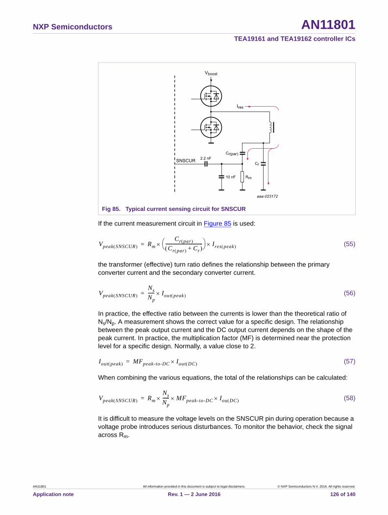
NXP Semiconductors AN11801TEA19161 and TEA19162 controller ICs
If the current measurement circuit in Figure 85 is used:
(55)
the transformer (effective) turn ratio defines the relationship between the primary converter current and the secondary converter current.
(56)
In practice, the effective ratio between the currents is lower than the theoretical ratio of Ns/Np. A measurement shows the correct value for a specific design. The relationship between the peak output current and the DC output current depends on the shape of the peak current. In practice, the multiplication factor (MF) is determined near the protection level for a specific design. Normally, a value close to 2.
(57)
When combining the various equations, the total of the relationships can be calculated:
(58)
It is difficult to measure the voltage levels on the SNSCUR pin during operation because a voltage probe introduces serious disturbances. To monitor the behavior, check the signal across Rm.
Fig 85. Typical current sensing circuit for SNSCUR
Vpeak SNSCUR Rm
Cr par
Cr par Cr+ ---------------------------------- Ires peak =
Vpeak SNSCUR Ns
Np------ Iout peak =
Iout peak MFpeak-to-DC Iout DC =
Vpeak SNSCUR Rm
Ns
Np------ MFpeak-to-DC Iou DC =
AN11801 All information provided in this document is subject to legal disclaimers. © NXP Semiconductors N.V. 2016. All rights reserved.
Application note Rev. 1 — 2 June 2016 126 of 140

NXP Semiconductors AN11801TEA19161 and TEA19162 controller ICs
14.2.7 Disabling the overcurrent protection (OCP)
The SNSCUR pin provides three functions:
• If the SNSCUR voltage Vbias exceeds 1.5 V, the gate driver is switched off to limit the power to the OCP level. After 5 OCP cycles, a protection is activated.
• If the SNSCUR voltage Vbias is at the level of 100 mV for detecting the (almost) zero current level, the driver switches off to prevent capacitive mode switching.
• If the SNSCUR voltage Vbias is at the level of 13 mV for detecting the current polarity, This level is used as a parameter in the internal switching logic.
When two diodes are connected anti-parallel to Rm, the OCP is disabled while the other two functions are still active.
Fig 86. SNSCUR OCP function disabled using two diodes
AN11801 All information provided in this document is subject to legal disclaimers. © NXP Semiconductors N.V. 2016. All rights reserved.
Application note Rev. 1 — 2 June 2016 127 of 140

NXP Semiconductors AN11801TEA19161 and TEA19162 controller ICs
14.2.8 Adapting trigger values for SNSCUR OCP and CMR
Normally, a suitable value for Rm can be found that works well for the OCP and the CMR functions. If finding a suitable value is not possible or critical, the circuit shown in Figure 87 can be used to set the trigger levels for OCP and CMR separately.
14.2.9 Internal OTP
When the internal junction temperature exceeds 140 C, the internal overtemperature protection is triggered. Either a latched protection disables HBC and PFC switching or the system restarts after the temperature has dropped.
14.2.10 OverPower Protection (OPP)
The OPP levels are related to Vhs(SNSCAP) and Vls(SNSCAP) on the SNSCAP pin. The chosen setting can be either 125 % or 150 % power (see Section 10.2).
Fig 87. SNSCUR: Different Rm resistor values for OCP and CMR
AN11801 All information provided in this document is subject to legal disclaimers. © NXP Semiconductors N.V. 2016. All rights reserved.
Application note Rev. 1 — 2 June 2016 128 of 140

xxxxxxxxxxxxxxxxxxxxx xxxxxxxxxxxxxxxxxxxxxxxxxx xxxxxxx x x x xxxxxxxxxxxxxxxxxxxxxxxxxxxxxx xxxxxxxxxxxxxxxxxxx xx xx xxxxx xxxxxxxxxxxxxxxxxxxxxxxxxxx xxxxxxxxxxxxxxxxxxx xxxxxx xxxxxxxxxxxxxxxxxxxxxxxxxxxxxxxxxxx xxxxxxxxxxxx x x xxxxxxxxxxxxxxxxxxxxx xxxxxxxxxxxxxxxxxxxxxxxxxxxxxx xxxxx xxxxxxxxxxxxxxxxxxxxxxxxxxxxxxxxxxxxxxxxxxxxxxxxxx xxxxxxxx xxxxxxxxxxxxxxxxxxxxxxxxx xxxxxxxxxxxxxxxxxxxx xxx
AN
11801
Ap
plicatio
n n
ote
Rev. 1 —
2 Jun
e 2016
129 of 140
NX
P S
emico
nd
ucto
rsA
N11801
TE
A1
9161
an
d T
EA
191
62 c
on
trolle
r ICs
15. Application example: 240 W power supply
All inform
ation provided
in this docum
ent is subject to leg
al disclaim
ers.©
NX
P S
em
iconductors N
.V. 2016. A
ll rights reserved.
15.1 Circuit diagrams
n.m. = not mounted
Fig 88. TEA1916 and TEA1995T 240 W power supply (PFC part)

NXP Semiconductors AN11801TEA19161 and TEA19162 controller ICs
n.m. = not mounted
Fig 89. TEA1916 and TEA1995T 240 W power supply (LLC part)
AN11801 All information provided in this document is subject to legal disclaimers. © NXP Semiconductors N.V. 2016. All rights reserved.
Application note Rev. 1 — 2 June 2016 130 of 140

NXP Semiconductors AN11801TEA19161 and TEA19162 controller ICs
n.m. = not mounted
Fig 90. TEA1916 and TEA1995T 240 W power supply (SR part)
AN11801 All information provided in this document is subject to legal disclaimers. © NXP Semiconductors N.V. 2016. All rights reserved.
Application note Rev. 1 — 2 June 2016 131 of 140

xxxxxxxxxxxxxxxxxxxxx xxxxxxxxxxxxxxxxxxxxxxxxxx xxxxxxx x x x xxxxxxxxxxxxxxxxxxxxxxxxxxxxxx xxxxxxxxxxxxxxxxxxx xx xx xxxxx xxxxxxxxxxxxxxxxxxxxxxxxxxx xxxxxxxxxxxxxxxxxxx xxxxxx xxxxxxxxxxxxxxxxxxxxxxxxxxxxxxxxxxx xxxxxxxxxxxx x x xxxxxxxxxxxxxxxxxxxxx xxxxxxxxxxxxxxxxxxxxxxxxxxxxxx xxxxx xxxxxxxxxxxxxxxxxxxxxxxxxxxxxxxxxxxxxxxxxxxxxxxxxx xxxxxxxx xxxxxxxxxxxxxxxxxxxxxxxxx xxxxxxxxxxxxxxxxxxxx xxx
AN
11801
Ap
plicatio
n n
ote
Rev. 1 —
2 Jun
e 2016
132 of 140
NX
P S
emico
nd
ucto
rsA
N11801
TE
A1
9161
an
d T
EA
191
62 c
on
trolle
r ICs
15.2 Circuit diagrams with function descriptions
All inform
ation provided
in this docum
ent is subject to leg
al disclaim
ers.©
NX
P S
em
iconductors N
.V. 2016. A
ll rights reserved.
n.m. = not mounted
Fig 91. TEA1916 and TEA1995T 240 W power supply (PFC part) with function descriptions

NXP Semiconductors AN11801TEA19161 and TEA19162 controller ICs
n.m. = not mounted
Fig 92. TEA1916 and TEA1995T 240 W power supply (LLC part) with function descriptions
AN11801 All information provided in this document is subject to legal disclaimers. © NXP Semiconductors N.V. 2016. All rights reserved.
Application note Rev. 1 — 2 June 2016 133 of 140
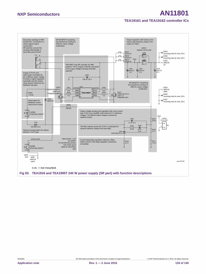
NXP Semiconductors AN11801TEA19161 and TEA19162 controller ICs
n.m. = not mounted
Fig 93. TEA1916 and TEA1995T 240 W power supply (SR part) with function descriptions
AN11801 All information provided in this document is subject to legal disclaimers. © NXP Semiconductors N.V. 2016. All rights reserved.
Application note Rev. 1 — 2 June 2016 134 of 140

NXP Semiconductors AN11801TEA19161 and TEA19162 controller ICs
15.3 PCB layout
16. Abbreviations
Fig 94. PCB layout (prototype)
Table 16. Abbreviations
Acronym Description
ADT Adaptive Dead Time
BCD Bipolar CMOS DMOS
CMR Capacitive Mode Regulation
EMC ElectroMagnetic Compatibility
EMI ElectroMagnetic Interference
HB Half Bridge (node, stage, or converter)
HBC Half-Bridge Converter (or Controller)
HP High-Power
HV High-Voltage
IC Integrated Circuit
LCD Liquid Crystal Display
LP Low-Power
MHR Mains Harmonics Reduction
OCP OverCurrent Protection
OLP Open-Loop Protection
OPP OverPower Protection
OTP OverTemperature Protection
OVP OverVoltage Protection
PCB Printed-Circuit Board
PWM Pulse Width Mode
QR Quasi-Resonant
AN11801 All information provided in this document is subject to legal disclaimers. © NXP Semiconductors N.V. 2016. All rights reserved.
Application note Rev. 1 — 2 June 2016 135 of 140

NXP Semiconductors AN11801TEA19161 and TEA19162 controller ICs
17. References
[1] TEA19161T data sheet — Digital controller for high-efficiency resonant power supply; 2016, NXP Semiconductors
[2] TEA19162T data sheet — PFC controller; 2016, NXP Semiconductors
[3] TEA19161CT data sheet — Digital controller for high-efficiency resonant power supply; 2016, NXP Semiconductors
[4] TEA19162CT data sheet — PFC controller; 2016, NXP Semiconductors
SCP Short-Circuit Protection
SOI Silicon-On Insulator
SMD Surface-Mounted Device
SR Synchronous Rectification
UVP UnderVoltage Protection
Table 16. Abbreviations …continued
Acronym Description
AN11801 All information provided in this document is subject to legal disclaimers. © NXP Semiconductors N.V. 2016. All rights reserved.
Application note Rev. 1 — 2 June 2016 136 of 140
NXP Semiconductors AN11801TEA19161 and TEA19162 controller ICs
18. Legal information
18.1 Definitions
Draft — The document is a draft version only. The content is still under internal review and subject to formal approval, which may result in modifications or additions. NXP Semiconductors does not give any representations or warranties as to the accuracy or completeness of information included herein and shall have no liability for the consequences of use of such information.
18.2 Disclaimers
Limited warranty and liability — Information in this document is believed to be accurate and reliable. However, NXP Semiconductors does not give any representations or warranties, expressed or implied, as to the accuracy or completeness of such information and shall have no liability for the consequences of use of such information. NXP Semiconductors takes no responsibility for the content in this document if provided by an information source outside of NXP Semiconductors.
In no event shall NXP Semiconductors be liable for any indirect, incidental, punitive, special or consequential damages (including - without limitation - lost profits, lost savings, business interruption, costs related to the removal or replacement of any products or rework charges) whether or not such damages are based on tort (including negligence), warranty, breach of contract or any other legal theory.
Notwithstanding any damages that customer might incur for any reason whatsoever, NXP Semiconductors’ aggregate and cumulative liability towards customer for the products described herein shall be limited in accordance with the Terms and conditions of commercial sale of NXP Semiconductors.
Right to make changes — NXP Semiconductors reserves the right to make changes to information published in this document, including without limitation specifications and product descriptions, at any time and without notice. This document supersedes and replaces all information supplied prior to the publication hereof.
Suitability for use — NXP Semiconductors products are not designed, authorized or warranted to be suitable for use in life support, life-critical or safety-critical systems or equipment, nor in applications where failure or malfunction of an NXP Semiconductors product can reasonably be expected to result in personal injury, death or severe property or environmental damage. NXP Semiconductors and its suppliers accept no liability for inclusion and/or use of NXP Semiconductors products in such equipment or applications and therefore such inclusion and/or use is at the customer’s own risk.
Applications — Applications that are described herein for any of these products are for illustrative purposes only. NXP Semiconductors makes no representation or warranty that such applications will be suitable for the specified use without further testing or modification.
Customers are responsible for the design and operation of their applications and products using NXP Semiconductors products, and NXP Semiconductors accepts no liability for any assistance with applications or customer product design. It is customer’s sole responsibility to determine whether the NXP
Semiconductors product is suitable and fit for the customer’s applications and products planned, as well as for the planned application and use of customer’s third party customer(s). Customers should provide appropriate design and operating safeguards to minimize the risks associated with their applications and products.
NXP Semiconductors does not accept any liability related to any default, damage, costs or problem which is based on any weakness or default in the customer’s applications or products, or the application or use by customer’s third party customer(s). Customer is responsible for doing all necessary testing for the customer’s applications and products using NXP Semiconductors products in order to avoid a default of the applications and the products or of the application or use by customer’s third party customer(s). NXP does not accept any liability in this respect.
Export control — This document as well as the item(s) described herein may be subject to export control regulations. Export might require a prior authorization from competent authorities.
Evaluation products — This product is provided on an “as is” and “with all faults” basis for evaluation purposes only. NXP Semiconductors, its affiliates and their suppliers expressly disclaim all warranties, whether express, implied or statutory, including but not limited to the implied warranties of non-infringement, merchantability and fitness for a particular purpose. The entire risk as to the quality, or arising out of the use or performance, of this product remains with customer.
In no event shall NXP Semiconductors, its affiliates or their suppliers be liable to customer for any special, indirect, consequential, punitive or incidental damages (including without limitation damages for loss of business, business interruption, loss of use, loss of data or information, and the like) arising out the use of or inability to use the product, whether or not based on tort (including negligence), strict liability, breach of contract, breach of warranty or any other theory, even if advised of the possibility of such damages.
Notwithstanding any damages that customer might incur for any reason whatsoever (including without limitation, all damages referenced above and all direct or general damages), the entire liability of NXP Semiconductors, its affiliates and their suppliers and customer’s exclusive remedy for all of the foregoing shall be limited to actual damages incurred by customer based on reasonable reliance up to the greater of the amount actually paid by customer for the product or five dollars (US$5.00). The foregoing limitations, exclusions and disclaimers shall apply to the maximum extent permitted by applicable law, even if any remedy fails of its essential purpose.
Translations — A non-English (translated) version of a document is for reference only. The English version shall prevail in case of any discrepancy between the translated and English versions.
18.3 TrademarksNotice: All referenced brands, product names, service names and trademarks are the property of their respective owners.
<Name> — is a trademark of NXP Semiconductors N.V. (replace by text inset t001tma<1nn>)
AN11801 All information provided in this document is subject to legal disclaimers. © NXP Semiconductors N.V. 2016. All rights reserved.
Application note Rev. 1 — 2 June 2016 137 of 140
NXP Semiconductors AN11801TEA19161 and TEA19162 controller ICs
19. Contents
1 Introduction . . . . . . . . . . . . . . . . . . . . . . . . . . . . 31.1 Related documents. . . . . . . . . . . . . . . . . . . . . . 31.2 Related products. . . . . . . . . . . . . . . . . . . . . . . . 3
2 TEA1916 highlights and features . . . . . . . . . . . 52.1 Resonant conversion . . . . . . . . . . . . . . . . . . . . 52.2 Power factor correction conversion . . . . . . . . . 52.3 TEA19161 and TEA19162 controller
combination . . . . . . . . . . . . . . . . . . . . . . . . . . . 62.4 Features and benefits . . . . . . . . . . . . . . . . . . . . 72.4.1 Distinctive features . . . . . . . . . . . . . . . . . . . . . . 72.4.2 Green features . . . . . . . . . . . . . . . . . . . . . . . . . 72.4.3 Protection features . . . . . . . . . . . . . . . . . . . . . . 72.5 Typical areas of application . . . . . . . . . . . . . . . 8
3 Pinning . . . . . . . . . . . . . . . . . . . . . . . . . . . . . . . . 93.1 TEA19161T (HBC) pin overview. . . . . . . . . . . . 93.2 TEA19162T (PFC) pin overview. . . . . . . . . . . 13
4 Application diagram . . . . . . . . . . . . . . . . . . . . 164.1 TEA19162. . . . . . . . . . . . . . . . . . . . . . . . . . . . 164.2 TEA19161T . . . . . . . . . . . . . . . . . . . . . . . . . . 17
5 Block diagram . . . . . . . . . . . . . . . . . . . . . . . . . 175.1 TEA19162T . . . . . . . . . . . . . . . . . . . . . . . . . . 175.2 TEA19161T . . . . . . . . . . . . . . . . . . . . . . . . . . 19
6 Supply functions and start-up . . . . . . . . . . . . 206.1 Basic supply system overview . . . . . . . . . . . . 206.2 SUPHV high-voltage supply . . . . . . . . . . . . . . 206.2.1 Start-up via the SUPHV pin . . . . . . . . . . . . . . 216.2.2 SUPHV pin during burst mode operation . . . . 236.2.3 SUPHV during protection . . . . . . . . . . . . . . . . 236.3 SUPIC supply using HBC transformer
auxiliary winding . . . . . . . . . . . . . . . . . . . . . . . 246.3.1 SUPIC supply using HBC transformer
auxiliary winding . . . . . . . . . . . . . . . . . . . . . . . 256.3.2 Voltage variations depending on auxiliary
winding position: primary side component . . . 256.4 SUPIC pin supply using external voltage . . . . 266.5 SUPREG pin. . . . . . . . . . . . . . . . . . . . . . . . . . 266.6 SUPHS pin . . . . . . . . . . . . . . . . . . . . . . . . . . . 276.6.1 Initial charging of the SUPHS pin . . . . . . . . . . 276.6.2 A lower voltage SUPHS pin . . . . . . . . . . . . . . 276.7 Capacitor values on the SUPIC, SUPREG,
and SUPHS pins. . . . . . . . . . . . . . . . . . . . . . . 286.7.1 The SUPIC pin . . . . . . . . . . . . . . . . . . . . . . . . 286.7.1.1 General . . . . . . . . . . . . . . . . . . . . . . . . . . . . . . 296.7.1.2 Start-up . . . . . . . . . . . . . . . . . . . . . . . . . . . . . . 296.7.1.3 Normal operation . . . . . . . . . . . . . . . . . . . . . . 296.7.1.4 Burst mode operation . . . . . . . . . . . . . . . . . . . 306.7.2 Value of the capacitor for the SUPREG pin . . 30
6.7.3 Value of the capacitor for the SUPHS pin . . . 30
7 MOSFET drivers (GATELS, GATEHS, and GATEPFC) . . . . . . . . . . . . . . . . . . . . . . . . . . . . 31
7.1 GATEPFC . . . . . . . . . . . . . . . . . . . . . . . . . . . 317.2 GATELS and GATEHS. . . . . . . . . . . . . . . . . . 317.3 MOSFET drivers - General information . . . . . 327.3.1 Switch-on . . . . . . . . . . . . . . . . . . . . . . . . . . . . 327.3.2 Switch-off . . . . . . . . . . . . . . . . . . . . . . . . . . . . 327.4 Specification of the gate drivers . . . . . . . . . . . 337.5 Limiting values for the high side driver
GATEHS, SUPHS, and HB . . . . . . . . . . . . . . 347.5.1 Supply voltage for the GATEHS output driver
(SUPHS pin) . . . . . . . . . . . . . . . . . . . . . . . . . 347.5.2 GATEHS switching. . . . . . . . . . . . . . . . . . . . . 357.5.3 HBC circuit behavior and the GATEHS pin . . 367.5.4 Limiting values SUPHS and HB. . . . . . . . . . . 397.5.5 GATEHS limits . . . . . . . . . . . . . . . . . . . . . . . . 397.5.5.1 GATEHS voltage . . . . . . . . . . . . . . . . . . . . . . 397.5.5.2 GATEHS current . . . . . . . . . . . . . . . . . . . . . . 397.6 Gate driver switch off and limiting values. . . . 407.6.1 Determining if switch-off reverse current is
still safe . . . . . . . . . . . . . . . . . . . . . . . . . . . . . 40
8 TEA19162 PFC functions . . . . . . . . . . . . . . . . 428.1 Mains voltage sensing and OTP
(SNSMAINS pin) . . . . . . . . . . . . . . . . . . . . . . 428.2 Mains voltage sensing (SNSMAINS pin) . . . . 438.3 Brownin and brownout (SNSMAINS pin) . . . . 448.4 NTC measurement for external OTP
(SNSMAINS pin) . . . . . . . . . . . . . . . . . . . . . . 448.5 PFC operation . . . . . . . . . . . . . . . . . . . . . . . . 458.6 PFC output power and peak current . . . . . . . 458.7 PFC output voltage regulation
(SNSBOOST pin). . . . . . . . . . . . . . . . . . . . . . 468.8 PFC gate driver (GATEPFC pin) . . . . . . . . . . 478.9 PFC on-time control . . . . . . . . . . . . . . . . . . . . 478.10 PFC soft start and soft stop (SNSCUR and
PFCCOM pins). . . . . . . . . . . . . . . . . . . . . . . . 478.11 PFCCOMP in the PFC voltage control loop. . 488.11.1 SNSBOOST error amplifier . . . . . . . . . . . . . . 488.11.2 PFCCOMP voltage . . . . . . . . . . . . . . . . . . . . 488.11.3 PFCCOMP network . . . . . . . . . . . . . . . . . . . . 498.11.4 Soft stop. . . . . . . . . . . . . . . . . . . . . . . . . . . . . 498.12 Mains compensation in the PFC voltage
control loop . . . . . . . . . . . . . . . . . . . . . . . . . . 508.13 PFC demagnetization sensing
(SNSAUX pin) . . . . . . . . . . . . . . . . . . . . . . . . 518.14 PFC valley sensing (SNSAUX pin) . . . . . . . . 51
AN11801 All information provided in this document is subject to legal disclaimers. © NXP Semiconductors N.V. 2016. All rights reserved.
Application note Rev. 1 — 2 June 2016 138 of 140
continued >>

NXP Semiconductors AN11801TEA19161 and TEA19162 controller ICs
8.15 PFC auxiliary sensing circuit. . . . . . . . . . . . . . 528.16 PFC frequency and off-time limiting . . . . . . . . 538.17 PFC overcurrent regulation, OCR-PFC
and soft start (SNSCUR pin). . . . . . . . . . . . . . 538.18 Active X-capacitor discharge . . . . . . . . . . . . . 548.18.1 Start active X-capacitor discharge . . . . . . . . . 558.18.2 X-capacitor discharge via a PFC MOSFET
operation. . . . . . . . . . . . . . . . . . . . . . . . . . . . . 558.18.3 X-capacitor discharge calculations . . . . . . . . . 568.18.3.1 Estimation of average discharge current . . . . 578.18.4 Reconnecting the mains voltage while
discharging . . . . . . . . . . . . . . . . . . . . . . . . . . . 588.18.5 Disabling X-capacitor discharge function . . . . 588.19 PFC burst mode . . . . . . . . . . . . . . . . . . . . . . . 598.19.1 PFC start and stop . . . . . . . . . . . . . . . . . . . . . 598.19.1.1 Stop PFC . . . . . . . . . . . . . . . . . . . . . . . . . . . . 598.19.1.2 Start PFC . . . . . . . . . . . . . . . . . . . . . . . . . . . . 598.19.1.3 Stop PFC (burst mode). . . . . . . . . . . . . . . . . . 598.19.2 SNSBOOST levels . . . . . . . . . . . . . . . . . . . . . 59
9 HBC (TEA19161) . . . . . . . . . . . . . . . . . . . . . . . 629.1 HBC start and SNSBOOST UVP . . . . . . . . . . 629.2 Power regulation using Vcap control . . . . . . . . 629.2.1 Sensing VSNSCAP with resistive and
capacitive divider . . . . . . . . . . . . . . . . . . . . . . 649.2.2 Scaling the VSNSCAP range to the
SNSCAP pin . . . . . . . . . . . . . . . . . . . . . . . . . . 649.2.3 Calculation of the SNSCAP divider value:
CSNSCAP(low) and CSNSCAP(high) . . . . . . . . . . . . 669.2.4 Practical restrictions for SNSCAP divider . . . . 679.2.5 SNSFB regulation. . . . . . . . . . . . . . . . . . . . . . 679.3 Operation modes . . . . . . . . . . . . . . . . . . . . . . 689.3.1 High-Power (HP) mode. . . . . . . . . . . . . . . . . . 699.3.2 Low-Power (LP) mode . . . . . . . . . . . . . . . . . . 699.3.2.1 LP-mode switching . . . . . . . . . . . . . . . . . . . . . 709.3.2.2 LP-mode with energy-per-cycle control . . . . . 719.3.2.3 LP mode with repetition frequency control . . . 729.3.3 Burst mode operation . . . . . . . . . . . . . . . . . . . 729.3.4 Mode presetting . . . . . . . . . . . . . . . . . . . . . . . 739.3.5 Mode transitions . . . . . . . . . . . . . . . . . . . . . . . 759.3.5.1 HP to LP transition . . . . . . . . . . . . . . . . . . . . . 759.3.5.2 LP to EC/RF transition . . . . . . . . . . . . . . . . . . 759.3.6 LP to BM transition . . . . . . . . . . . . . . . . . . . . . 769.3.7 Capacitive mode prevention using the
SNSCUR pin. . . . . . . . . . . . . . . . . . . . . . . . . . 779.3.7.1 Practical application of CMR switching. . . . . . 779.3.7.2 Measuring the voltage on the SNSCUR pin . . 779.3.7.3 Example of CMR switching in a test
condition . . . . . . . . . . . . . . . . . . . . . . . . . . . . . 78
10 Presetting TEA1916 functionality and power good . . . . . . . . . . . . . . . . . . . . . . . . . . . . . . . . . 80
10.1 Setting the soft start power level (RGATELS) . . 8110.2 Protection mode and OPP setting
(SNSSET resistor R1) . . . . . . . . . . . . . . . . . . 8210.3 Power Good (PG) function. . . . . . . . . . . . . . . 8310.4 SNSSET R2: Power level for HP/LP
transition . . . . . . . . . . . . . . . . . . . . . . . . . . . . 8410.5 Capacitor value for the SNSSET pin . . . . . . . 8510.6 RSNSOUT: Burst repetition frequency. . . . . . . . 8510.7 Burst mode transition level: SNSSET R2
and RSNSOUT . . . . . . . . . . . . . . . . . . . . . . . . . 8610.7.1 Time delay VSNSCAP to HB transition . . . . . . . 8610.7.2 Accuracy of mode transition levels . . . . . . . . 8710.8 Modify power levels for HP-to-LP and
burst mode transition . . . . . . . . . . . . . . . . . . . 8810.8.1 Adding an offset to the SNSCAP signal
to modify (transition) power levels . . . . . . . . . 8810.8.2 Example of changed mode transition
power levels . . . . . . . . . . . . . . . . . . . . . . . . . . 89
11 Standby or no-load condition in burst mode operation . . . . . . . . . . . . . . . . . . . . . . . . . . . . . 91
11.1 No-load power consumption . . . . . . . . . . . . . 9111.1.1 Power consumption of feedback circuit
and output resistive divider . . . . . . . . . . . . . . 9211.1.2 Power consumption of TEA19161 and TEA19162
SUPIC . . . . . . . . . . . . . . . . . . . . . . . . . . . . . . 9211.1.3 Power consumption of SNSMAINS . . . . . . . . 9311.1.4 Power consumption of the resistive divider
part for SNSCAP . . . . . . . . . . . . . . . . . . . . . . 9311.1.5 Power consumption of the resistive divider
for SNSBOOST . . . . . . . . . . . . . . . . . . . . . . . 9311.1.6 Power consumption estimation at very
low load condition . . . . . . . . . . . . . . . . . . . . . 9311.2 Audible noise . . . . . . . . . . . . . . . . . . . . . . . . . 9311.2.1 Audible noise PFC converter . . . . . . . . . . . . . 9411.2.2 Audible noise HBC converter. . . . . . . . . . . . . 9411.2.3 Measures in the coil and transformer
construction . . . . . . . . . . . . . . . . . . . . . . . . . . 94
12 Practical system implementation topics. . . . 9612.1 Questions and answers on settings options . 9612.2 Questions and answers on debugging. . . . . . 9712.3 Start-up and debugging . . . . . . . . . . . . . . . . . 9812.3.1 HBC only operation with DC boost voltage . . 9812.3.2 PFC only operation . . . . . . . . . . . . . . . . . . . 10012.3.3 Splitting SNSBOOST for PFC and
HBC operation . . . . . . . . . . . . . . . . . . . . . . . 10112.3.4 Checking the SNSCAP divider. . . . . . . . . . . 10212.4 Load sweep for checking the mode
transitions and the behavior. . . . . . . . . . . . . 10312.5 Converter with two output voltages . . . . . . . 104
AN11801 All information provided in this document is subject to legal disclaimers. © NXP Semiconductors N.V. 2016. All rights reserved.
Application note Rev. 1 — 2 June 2016 139 of 140
continued >>

NXP Semiconductors AN11801TEA19161 and TEA19162 controller ICs
12.5.1 Regulation of two output voltages usingshared feedback . . . . . . . . . . . . . . . . . . . . . . 105
12.5.2 Output voltage coupling by connectingoutput capacitors . . . . . . . . . . . . . . . . . . . . . 106
12.6 Checking limiting values in an application . . 10612.6.1 Measuring recommendations . . . . . . . . . . . . 10712.6.1.1 Measurement to estimate the signal level
added to the result by the voltage probe . . . 10712.6.1.2 Extra check: Adding a peak rectifier circuit
to the measurement probe . . . . . . . . . . . . . . 10712.6.2 TEA19161 VSUPHS, VHB, VGATEHS, VGATELS,
and TEA19162 VGATEPFC limiting values . . . 10812.6.3 TEA19161 and TEA19162 VSUPIC
limiting values . . . . . . . . . . . . . . . . . . . . . . . . 10812.6.4 TEA19161 VSUPREG limiting values . . . . . . . 10912.6.5 TEA19161 VSNSFB limiting values. . . . . . . . . 10912.6.6 TEA19161 VSNSOUT limiting values . . . . . . . 10912.6.7 TEA19161 VSNSSET limiting values. . . . . . . . 10912.6.8 TEA19161 VSNSCUR limiting values . . . . . . . 10912.6.9 TEA19161 VSNSCAP limiting values. . . . . . . . 11012.6.10 TEA19161 VSNSBOOST limiting values. . . . . . 11012.6.11 TEA19162 VSNSMAINS limiting values . . . . . . 11012.6.12 TEA19162 VPFCCOMP limiting values . . . . . . 11012.6.13 TEA19162 VSNSAUX limiting values. . . . . . . . 11112.6.14 TEA19162 VSNSCUR limiting values . . . . . . . 11112.6.15 TEA19162 VSNSBOOST limiting values. . . . . . 111
13 Important PCB layout design rules . . . . . . . 11213.1 Short SNSBOOST track length . . . . . . . . . . 11213.2 TEA19161: Shielding the SNSFB track . . . . 11313.3 TL431 circuit must be compact. . . . . . . . . . . 11413.4 Separate GND connections for TEA19161
and TEA19162 . . . . . . . . . . . . . . . . . . . . . . . 11413.5 TEA19161: Very short SNSCUR track . . . . . 11513.6 TEA19162: placing of SNSMAINS mains
sensing resistors. . . . . . . . . . . . . . . . . . . . . . 116
14 Protections . . . . . . . . . . . . . . . . . . . . . . . . . . . 11714.1 PFC protections . . . . . . . . . . . . . . . . . . . . . . 11814.1.1 UVP SUPIC . . . . . . . . . . . . . . . . . . . . . . . . . 11814.1.2 OverTemperature Protection (OTP) . . . . . . . 11814.1.2.1 Internal OTP . . . . . . . . . . . . . . . . . . . . . . . . . 11814.1.2.2 External OTP . . . . . . . . . . . . . . . . . . . . . . . . 11814.1.2.3 Not using the external OTP function. . . . . . . 11814.1.3 UVP SNSMAINS (brownout) . . . . . . . . . . . . 11914.1.4 OVP SNSBOOST . . . . . . . . . . . . . . . . . . . . . 11914.1.5 SCP and OLP SNSBOOST . . . . . . . . . . . . . 11914.1.6 OCP SNSCUR . . . . . . . . . . . . . . . . . . . . . . . 11914.2 HBC protections . . . . . . . . . . . . . . . . . . . . . . 11914.2.1 UVP SUPIC and SUPREG . . . . . . . . . . . . . . 11914.2.2 UVP SUPHS. . . . . . . . . . . . . . . . . . . . . . . . . 12014.2.3 UVP SNSBOOST . . . . . . . . . . . . . . . . . . . . . 120
14.2.4 OVP on the SNSOUT pin. . . . . . . . . . . . . . . 12014.2.4.1 Time delay until protection . . . . . . . . . . . . . . 12114.2.4.2 Auxiliary winding construction for OVP
sensing. . . . . . . . . . . . . . . . . . . . . . . . . . . . . 12114.2.4.3 Calculation of OVP sensing using auxiliary
winding. . . . . . . . . . . . . . . . . . . . . . . . . . . . . 12114.2.4.4 Differences between theory and practice:
calibration. . . . . . . . . . . . . . . . . . . . . . . . . . . 12214.2.4.5 Example of calibration and an estimation of
tolerance . . . . . . . . . . . . . . . . . . . . . . . . . . . 12314.2.4.6 Output voltage increase because of
time delay. . . . . . . . . . . . . . . . . . . . . . . . . . . 12414.2.4.7 OVP triggering using an external signal. . . . 12414.2.4.8 Disabling the OVP function on the
SNSOUT pin . . . . . . . . . . . . . . . . . . . . . . . . 12514.2.5 Capacitive Mode Regulation (CMR) . . . . . . 12514.2.6 Overcurrent protection (OCP) on the
SNSCUR pin . . . . . . . . . . . . . . . . . . . . . . . . 12514.2.7 Disabling the overcurrent protection
(OCP). . . . . . . . . . . . . . . . . . . . . . . . . . . . . . 12714.2.8 Adapting trigger values for SNSCUR OCP
and CMR . . . . . . . . . . . . . . . . . . . . . . . . . . . 12814.2.9 Internal OTP. . . . . . . . . . . . . . . . . . . . . . . . . 12814.2.10 OverPower Protection (OPP). . . . . . . . . . . . 128
15 Application example: 240 W powersupply. . . . . . . . . . . . . . . . . . . . . . . . . . . . . . . 129
15.1 Circuit diagrams . . . . . . . . . . . . . . . . . . . . . . 12915.2 Circuit diagrams with function
descriptions . . . . . . . . . . . . . . . . . . . . . . . . . 13215.3 PCB layout . . . . . . . . . . . . . . . . . . . . . . . . . . 135
16 Abbreviations . . . . . . . . . . . . . . . . . . . . . . . . 135
17 References. . . . . . . . . . . . . . . . . . . . . . . . . . . 136
18 Legal information . . . . . . . . . . . . . . . . . . . . . 13718.1 Definitions . . . . . . . . . . . . . . . . . . . . . . . . . . 13718.2 Disclaimers . . . . . . . . . . . . . . . . . . . . . . . . . 13718.3 Trademarks . . . . . . . . . . . . . . . . . . . . . . . . . 137
19 Contents. . . . . . . . . . . . . . . . . . . . . . . . . . . . . 138
© NXP Semiconductors N.V. 2016. All rights reserved.
For more information, please visit: http://www.nxp.comFor sales office addresses, please send an email to: [email protected]
Date of release: 2 June 2016
Document identifier: AN11801
Please be aware that important notices concerning this document and the product(s)described herein, have been included in section ‘Legal information’.
Related Documents