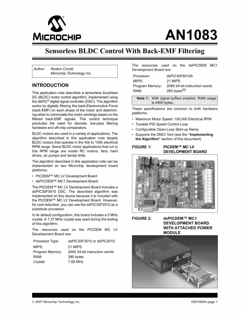
© 2007 Microchip Technology Inc. DS01083A-page 1 AN1083 INTRODUCTION This application note describes a sensorless brushless DC (BLDC) motor control algorithm, implemented using the dsPIC fi digital signal controller (DSC). The algorithm works by digitally filtering the back-Electromotive Force (back-EMF) on each phase of the motor and determin- ing when to commutate the motor windings based on the filtered back-EMF signals. This control technique precludes the need for discrete, low-pass filtering hardware and off-chip comparators. BLDC motors are used in a variety of applications. The algorithm described in this application note targets BLDC motors that operate in the 40k to 100k electrical RPM range. Some BLDC motor applications that run in this RPM range are model RC motors, fans, hard drives, air pumps and dental drills. The algorithm described in this application note can be implemented on two Microchip development board platforms: PICDEM™ MC LV Development Board dsPICDEM™ MC1 Development Board The PICDEM™ MC LV Development Board includes a dsPIC30F3010 DSC. The described algorithm was implemented on this device because it is included with the PICDEM™ MC LV Development Board. However, for cost reduction, you can use the dsPIC30F2010 as a substitute processor. In its default configuration, this board includes a 5 MHz crystal. A 7.37 MHz crystal was used during the testing of this algorithm. The resources used on the PICDEM MC LV Development Board are: The resources used on the dsPICDEM MC1 Development Board are: These specifications are common to both hardware platforms: Maximum Motor Speed: 100,000 Electrical RPM Tunable PID Speed Control Loop Configurable Open-Loop Start-up Ramp Supports the DMCI Tool (see the Implementing the Algorithm section of this document) FIGURE 1: PICDEM™ MC LV DEVELOPMENT BOARD FIGURE 2: dsPICDEM™ MC1 DEVELOPMENT BOARD WITH ATTACHED POWER MODULE Processor Type: dsPIC30F3010 or dsPIC2010 MIPS: 21 MIPS Program Memory: 2000 24-bit instruction words RAM: 280 bytes Crystal: 7.68 MHz Author: Reston Condit Microchip Technology Inc. Processor: dsPIC30F6010A MIPS: 21 MIPS Program Memory: 2089 24-bit instruction words RAM: 280 bytes (1) Note 1: With signal buffers enabled, RAM usage is 4400 bytes. Sensorless BLDC Control With Back-EMF Filtering

Welcome message from author
This document is posted to help you gain knowledge. Please leave a comment to let me know what you think about it! Share it to your friends and learn new things together.
Transcript
AN1083Sensorless BLDC Control With Back-EMF Filtering
INTRODUCTIONThis application note describes a sensorless brushlessDC (BLDC) motor control algorithm, implemented usingthe dsPIC® digital signal controller (DSC). The algorithmworks by digitally filtering the back-Electromotive Force(back-EMF) on each phase of the motor and determin-ing when to commutate the motor windings based on thefiltered back-EMF signals. This control techniqueprecludes the need for discrete, low-pass filteringhardware and off-chip comparators.
BLDC motors are used in a variety of applications. Thealgorithm described in this application note targetsBLDC motors that operate in the 40k to 100k electricalRPM range. Some BLDC motor applications that run inthis RPM range are model RC motors, fans, harddrives, air pumps and dental drills.
The algorithm described in this application note can beimplemented on two Microchip development boardplatforms:
� PICDEM� MC LV Development Board� dsPICDEM� MC1 Development Board
The PICDEM� MC LV Development Board includes adsPIC30F3010 DSC. The described algorithm wasimplemented on this device because it is included withthe PICDEM� MC LV Development Board. However,for cost reduction, you can use the dsPIC30F2010 as asubstitute processor.
In its default configuration, this board includes a 5 MHzcrystal. A 7.37 MHz crystal was used during the testingof this algorithm.
The resources used on the PICDEM MC LVDevelopment Board are:
The resources used on the dsPICDEM MC1Development Board are:
These specifications are common to both hardwareplatforms:
� Maximum Motor Speed: 100,000 Electrical RPM� Tunable PID Speed Control Loop� Configurable Open-Loop Start-up Ramp� Supports the DMCI Tool (see the �Implementing
the Algorithm� section of this document)
FIGURE 1: PICDEM� MC LV DEVELOPMENT BOARD
FIGURE 2: dsPICDEM� MC1 DEVELOPMENT BOARD WITH ATTACHED POWER MODULE
Processor Type: dsPIC30F3010 or dsPIC2010MIPS: 21 MIPSProgram Memory: 2000 24-bit instruction words RAM: 280 bytesCrystal: 7.68 MHz
Author: Reston ConditMicrochip Technology Inc.
Processor: dsPIC30F6010AMIPS: 21 MIPSProgram Memory: 2089 24-bit instruction wordsRAM: 280 bytes(1)
Note 1: With signal buffers enabled, RAM usageis 4400 bytes.
© 2007 Microchip Technology Inc. DS01083A-page 1
AN1083
BLDC MOTOR CONSTRUCTIONThis algorithm has been tested on these motors:
� 4-pole, 12V, 10A fan motor with a maximum speed of 29,000 RPM
� 14-pole, 12V model airplane motor with a maximum speed of 13,000 RPM
� 4-pole, 24V, 1A Hurst BLDC motor model DMB0224C10002
These motors have been tested with loads that areproportional to speed � they have light loads at lowspeed and full loads at high speed.
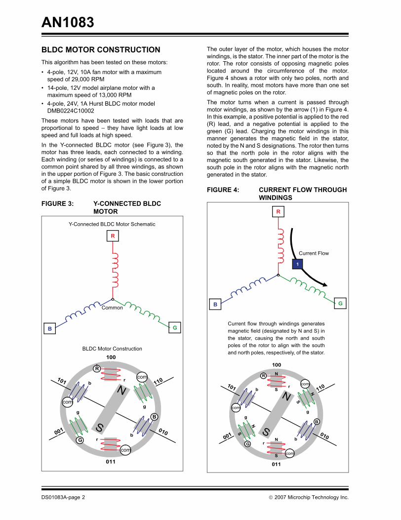
In the Y-connected BLDC motor (see Figure 3), themotor has three leads, each connected to a winding.Each winding (or series of windings) is connected to acommon point shared by all three windings, as shownin the upper portion of Figure 3. The basic constructionof a simple BLDC motor is shown in the lower portionof Figure 3.
FIGURE 3: Y-CONNECTED BLDC MOTOR
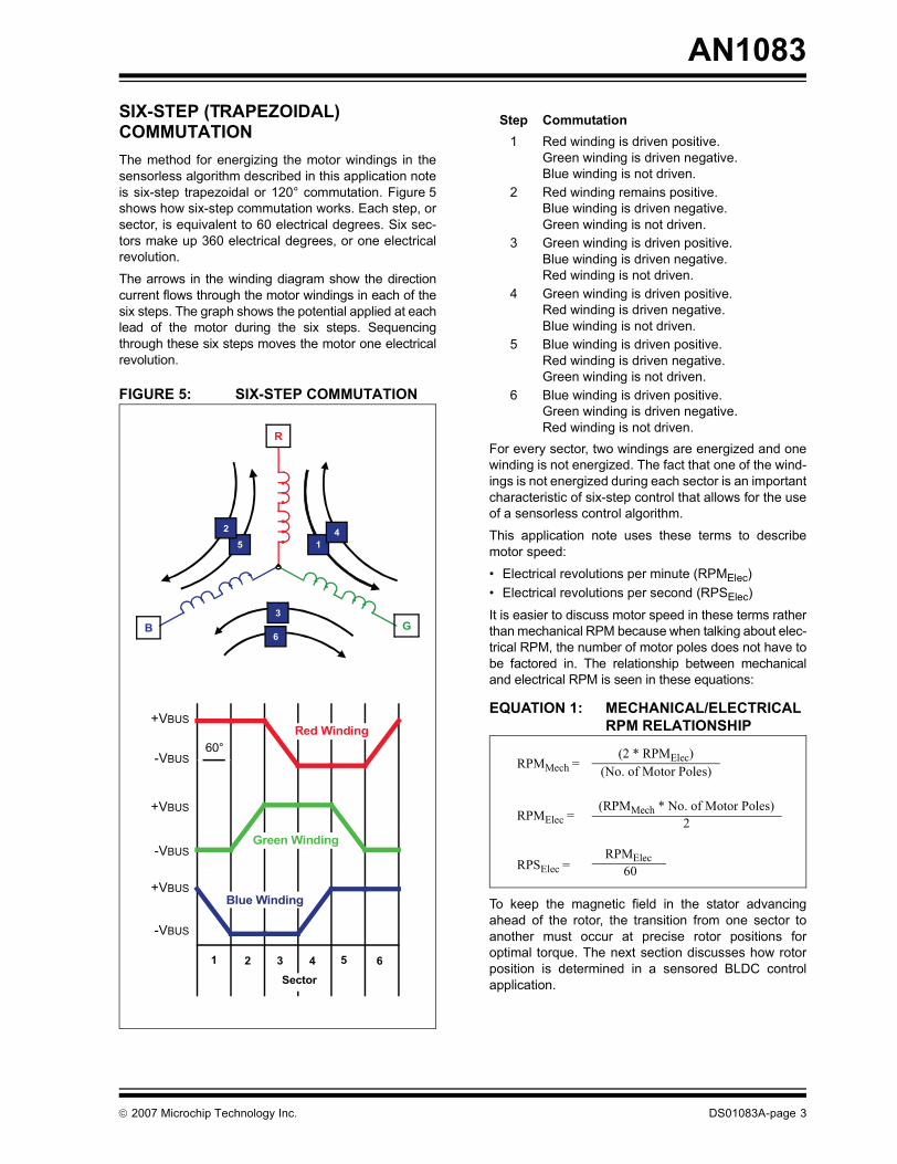
The outer layer of the motor, which houses the motorwindings, is the stator. The inner part of the motor is therotor. The rotor consists of opposing magnetic poleslocated around the circumference of the motor.Figure 4 shows a rotor with only two poles, north andsouth. In reality, most motors have more than one setof magnetic poles on the rotor.
The motor turns when a current is passed throughmotor windings, as shown by the arrow (1) in Figure 4.In this example, a positive potential is applied to the red(R) lead, and a negative potential is applied to thegreen (G) lead. Charging the motor windings in thismanner generates the magnetic field in the stator,noted by the N and S designations. The rotor then turnsso that the north pole in the rotor aligns with themagnetic south generated in the stator. Likewise, thesouth pole in the rotor aligns with the magnetic northgenerated in the stator.
FIGURE 4: CURRENT FLOW THROUGH WINDINGS
R
GB
100
N
S
R
B
r
r
gg
b
bG
com
com
com
110
010
011
101
001
Y-Connected BLDC Motor Schematic
BLDC Motor Construction
Common
R
GB
1
100
N
S
R
B
r
r
gg
b
bG
com
com
com
N
N
S
S
N
N
S
S 110
010
011
101
001
Current Flow
Current flow through windings generatesmagnetic field (designated by N and S) inthe stator, causing the north and southpoles of the rotor to align with the southand north poles, respectively, of the stator.
DS01083A-page 2 © 2007 Microchip Technology Inc.
AN1083
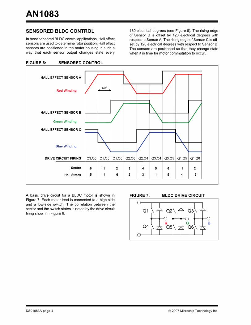
SIX-STEP (TRAPEZOIDAL) COMMUTATIONThe method for energizing the motor windings in thesensorless algorithm described in this application noteis six-step trapezoidal or 120° commutation. Figure 5shows how six-step commutation works. Each step, orsector, is equivalent to 60 electrical degrees. Six sec-tors make up 360 electrical degrees, or one electricalrevolution.
The arrows in the winding diagram show the directioncurrent flows through the motor windings in each of thesix steps. The graph shows the potential applied at eachlead of the motor during the six steps. Sequencingthrough these six steps moves the motor one electricalrevolution.
FIGURE 5: SIX-STEP COMMUTATION
For every sector, two windings are energized and onewinding is not energized. The fact that one of the wind-ings is not energized during each sector is an importantcharacteristic of six-step control that allows for the useof a sensorless control algorithm.
This application note uses these terms to describemotor speed:
� Electrical revolutions per minute (RPMElec)� Electrical revolutions per second (RPSElec)
It is easier to discuss motor speed in these terms ratherthan mechanical RPM because when talking about elec-trical RPM, the number of motor poles does not have tobe factored in. The relationship between mechanicaland electrical RPM is seen in these equations:
EQUATION 1: MECHANICAL/ELECTRICAL RPM RELATIONSHIP
To keep the magnetic field in the stator advancingahead of the rotor, the transition from one sector toanother must occur at precise rotor positions foroptimal torque. The next section discusses how rotorposition is determined in a sensored BLDC controlapplication.
R
GB
154
6
2
3
60°
1 2 3 4 5 6
Blue Winding
Green Winding
Red Winding
Sector
+VBUS
-VBUS
+VBUS
-VBUS
-VBUS
+VBUS
Step Commutation1 Red winding is driven positive.
Green winding is driven negative.Blue winding is not driven.
2 Red winding remains positive.Blue winding is driven negative.Green winding is not driven.
3 Green winding is driven positive.Blue winding is driven negative.Red winding is not driven.
4 Green winding is driven positive.Red winding is driven negative.Blue winding is not driven.
5 Blue winding is driven positive.Red winding is driven negative.Green winding is not driven.
6 Blue winding is driven positive.Green winding is driven negative.Red winding is not driven.
RPMMech =(2 * RPMElec)
(No. of Motor Poles)
RPMElec =(RPMMech * No. of Motor Poles)
2
RPSElec = RPMElec
60
© 2007 Microchip Technology Inc. DS01083A-page 3
AN1083
SENSORED BLDC CONTROLIn most sensored BLDC control applications, Hall effectsensors are used to determine rotor position. Hall effectsensors are positioned in the motor housing in such away that each sensor output changes state every
180 electrical degrees (see Figure 6). The rising edgeof Sensor B is offset by 120 electrical degrees withrespect to Sensor A. The rising edge of Sensor C is off-set by 120 electrical degrees with respect to Sensor B.The sensors are positioned so that they change statewhen it is time for motor commutation to occur.
FIGURE 6: SENSORED CONTROL
A basic drive circuit for a BLDC motor is shown inFigure 7. Each motor lead is connected to a high-sideand a low-side switch. The correlation between thesector and the switch states is noted by the drive circuitfiring shown in Figure 6.
FIGURE 7: BLDC DRIVE CIRCUIT
DRIVE CIRCUIT FIRING
Green Winding
Q1,Q5 Q1,Q6 Q2,Q6 Q2,Q4 Q3,Q4 Q3,Q5
60°
HALL EFFECT SENSOR A
HALL EFFECT SENSOR B
HALL EFFECT SENSOR C
Q1,Q5 Q1,Q6Q3,Q5
Sector 6
Hall States
1 2 3
5 4 6 2
4
3
5
1
6
5
1
4
2
6
Blue Winding
Red Winding
BR G
Q1 Q3Q2
Q4 Q6Q5
DS01083A-page 4 © 2007 Microchip Technology Inc.
AN1083
WHY SENSORLESS CONTROL?In sensored control, sensors determine the position ofthe motor rotor with respect to the motor stator. Thismakes for fairly simple control of the motor. A processorneed only wait for a Hall effect sensor to change state,determine which sector the rotor is in based on the out-put of the three Hall effect sensors and commutate themotor windings appropriately.
Sensored control has several drawbacks:
� Sensors cost money. In addition to the sensor itself, there is the further cost of mounting the sensors to the motor during manufacturing as well as the cost of sensor wires.
� Sensors add another potential failure point to the motor. If a sensor fails, the motor fails.
� In some environments it is just not practical to use sensors. For instance, in an environment where the motor is flooded (like a compressor or pump), the sensors may be subject to failure before the rest of the motor.
For these and other reasons, sensorless BLDC controlis desirable in many applications. The next sectionintroduces the theory behind the sensorless BLDCcontrol technique described in this application note.
SENSORLESS BLDC CONTROL The key to determining the appropriate moment whenthe motor winding should be commutated, or transitionfrom one sector to another, is the rotor position. Withsensored control, the rotor position is immediately evi-dent. However, in sensorless control, rotor positionmust be determined by a means other than sensors.
The method chosen for this algorithm is to analyze theback-Electromotive Force (EMF) from the motor. Insimplest terms, back-EMF is the voltage generated inthe stator winding by a permanent magnet motor whenthe rotor of the motor is turning. The magnitude ofback-EMF is proportional to the speed of the motor.
Figure 8 will help to explain back-EMF. This figureshows the potential of the three leads of a motor as itturns using sensored control. The shape of the threesignals is very similar to the trapezoidal shape shownin Figure 5. Vertical lines have been added to the graphto help identify the six sectors. A PWM signal is provid-ing power to each winding. During every third sector,Phase A, for example, is not being driven. However,some voltage is still seen at the lead of the motor duringthe non-driven sector for a particular phase. Thisvoltage is the back-EMF.
FIGURE 8: BACK-EMF
Phase A
Phase B
Phase C
Note: These waveforms were captured using a dsPIC3F6010A to sample the signals at the leads of a runningBLDC motor. The samples are displayed using the Data Monitor and Control Interface (DMCI) tool avail-able in MPLAB® IDE. The DMCI tool is discussed in greater detail in the �Implementing the Algorithm�section of this document.
© 2007 Microchip Technology Inc. DS01083A-page 5
AN1083
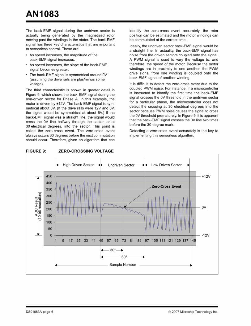
The back-EMF signal during the undriven sector isactually being generated by the magnetized rotormoving past the windings in the stator. The back-EMFsignal has three key characteristics that are importantto sensorless control. These are:� As speed increases, the magnitude of the back-EMF signal increases.
� As speed increases, the slope of the back-EMF signal becomes greater.
� The back-EMF signal is symmetrical around 0V (assuming the drive rails are plus/minus some voltage).
The third characteristic is shown in greater detail inFigure 9, which shows the back-EMF signal during thenon-driven sector for Phase A. In this example, themotor is driven by ±12V. The back-EMF signal is sym-metrical about 0V. (If the drive rails were 12V and 0V,the signal would be symmetrical at about 6V.) If theback-EMF signal was a straight line, the signal wouldcross the 0V line halfway through the sector, or at30 electrical degrees, into the sector. This point iscalled the zero-cross event. The zero-cross eventalways occurs 30 degrees before the next commutationshould occur. Therefore, given an algorithm that can
identify the zero-cross event accurately, the rotorposition can be estimated and the motor windings canbe commutated at the correct time.
Ideally, the undriven sector back-EMF signal would bea straight line. In actuality, the back-EMF signal hasnoise from the driven sectors coupled onto the signal.A PWM signal is used to vary the voltage to, andtherefore, the speed of the motor. Because the motorwindings are in proximity to one another, the PWMdrive signal from one winding is coupled onto theback-EMF signal of another winding.
It is difficult to detect the zero-cross event due to thecoupled PWM noise. For instance, if a microcontrolleris instructed to identify the first time the back-EMFsignal crosses the 0V threshold in the undriven sectorfor a particular phase, the microcontroller does notdetect the crossing at 30 electrical degrees into thesector because PWM noise causes the signal to crossthe 0V threshold prematurely. In Figure 9, it is apparentthat the back-EMF signal crosses the 0V line two timesbefore the 30-degree mark.
Detecting a zero-cross event accurately is the key toimplementing this sensorless algorithm.
FIGURE 9: ZERO-CROSSING VOLTAGE
0
50
100
150
200
250
300
350
400
450
1 9 17 25 33 41 49 57 65 73 81 89 97 105 113 121 129 137 145
+12V
-12V
0V
High Driven Sector Low Driven SectorUndriven Sector
30°
60°
Zero-Cross Event
ADC
Res
ult
Sample Number
(10-
bit r
esol
utio
n)
DS01083A-page 6 © 2007 Microchip Technology Inc.
AN1083
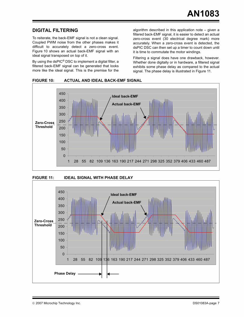
DIGITAL FILTERINGTo reiterate, the back-EMF signal is not a clean signal.Coupled PWM noise from the other phases makes itdifficult to accurately detect a zero-cross event.Figure 10 shows an actual back-EMF signal with anideal signal transposed on top of it.
By using the dsPIC® DSC to implement a digital filter, afiltered back-EMF signal can be generated that looksmore like the ideal signal. This is the premise for the
algorithm described in this application note � given afiltered back-EMF signal, it is easier to detect an actualzero-cross event (30 electrical degree mark) moreaccurately. When a zero-cross event is detected, thedsPIC DSC can then set up a timer to count down untilit is time to commutate the motor windings.
Filtering a signal does have one drawback, however.Whether done digitally or in hardware, a filtered signalexhibits some phase delay as compared to the actualsignal. The phase delay is illustrated in Figure 11.
FIGURE 10: ACTUAL AND IDEAL BACK-EMF SIGNAL
FIGURE 11: IDEAL SIGNAL WITH PHASE DELAY
0
50
100
150
200
250
300
350
400
450
1 28 55 82 109 136 163 190 217 244 271 298 325 352 379 406 433 460 487
Ideal back-EMF
Actual back-EMF
Zero-Cross Threshold
0
50
100
150
200
250
300
350
400
450
1 28 55 82 109 136 163 190 217 244 271 298 325 352 379 406 433 460 487
Ideal back-EMF
Actual back-EMF
Zero-Cross Threshold
Phase Delay
© 2007 Microchip Technology Inc. DS01083A-page 7
AN1083
Fortunately, when a digital filter is used, the phasedelay can be calculated given the filter specificationsand the frequency of the back-EMF signal. The calcu-lated phase delay can then be subtracted from thecount-down timer.For this algorithm, the Microchip dsPIC DSC DigitalFilter Design tool was used to design the back-EMFfilter. This design tool automatically calculates phasedelay for the filter. The next few paragraphs describehow the dsPIC DSC Digital Filter Design tool was usedto design a filter for the 20 kHz PWM signal.
The Digital Filter Design tool requires the followinginputs:
� Filter Type� Sampling Frequency� Pass-Band Frequency� Stop-Band Frequency� Pass-Band Ripple (db)� Stop-Band Ripple (db)� Filter Order
For this implementation, an IIR filter was choseninstead of an FIR filter because an IIR filter takes lesstime to execute. An FIR filter requires a much higherorder when compared to an IIR filter with similarresponse characteristics. In addition, the phase delayperiod is much less for an IIR filter verses a FIR filterwith a similar response.
The filter parameters used in this algorithm are listed inTable 1.
TABLE 1: FILTER PARAMETERS
Once these parameters are specified, the dsPIC DSCDigital Filter Design tool calculates the IIR filter coeffi-cients and generates the necessary source and headerfiles for implementing the filter. These files have beenadded to the sensorless BLDC motor control project inMPLAB® IDE.
The dsPIC DSC Digital Filter Design tool providesseveral graphs showing the response of the filter.These graphs include:
� Magnitude vs. Frequency� Log Magnitude vs. Frequency� Phase vs. Frequency� Group Delay vs. Frequency� Impulse Response vs. Time� Step Response vs. Time
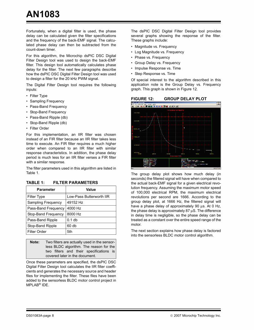
Of special interest to the algorithm described in thisapplication note is the Group Delay vs. Frequencygraph. This graph is shown in Figure 12.
FIGURE 12: GROUP DELAY PLOT
The group delay plot shows how much delay (inseconds) the filtered signal will have when compared tothe actual back-EMF signal for a given electrical revo-lution frequency. Assuming the maximum motor speedof 100,000 electrical RPM, the maximum electricalrevolutions per second are 1666. According to thegroup delay plot, at 1666 Hz, the filtered signal willhave a phase delay of approximately 90 μs. At 0 Hz,the phase delay is approximately 87 μS. The differencein delay time is negligible, so the phase delay can betreated as a constant over the entire speed range of themotor.
The next section explains how phase delay is factoredinto the sensorless BLDC motor control algorithm.
Parameter Value
Filter Type Low-Pass Butterworth IIR Sampling Frequency 49152 HzPass-Band Frequency 4000 HzStop-Band Frequency 8000 HzPass-Band Ripple 0.1 dbStop-Band Ripple 60 dbFilter Order 5th
Note: Two filters are actually used in the sensor-less BLDC algorithm. The reason for thetwo filters and their specifications iscovered later in the document.
DS01083A-page 8 © 2007 Microchip Technology Inc.
AN1083
CHARACTERISTICS OF BACK-EMFThe characteristics of the back-EMF signal are quitedifferent when the motor is turning slowly versusturning fast. As a result, the sensorless BLDC controlalgorithm analyzes the back-EMF in one of two ways,based on the speed of the motor. To understand whythere are two implementations, it is necessary to lookat the characteristics of the back-EMF signal at bothlow and high motor speeds.
Low-Speed back-EMF CharacteristicsAt very low speed, no noticeable back-EMF is gener-ated. The back-EMF signal is essentially flat during thenon-driven sector for a particular phase. Consequently,the zero-cross point is indistinguishable. As the motorturns faster, the back-EMF signal eventually begins tohave some slope.
A sensorless algorithm will not work unless there issufficient slope in the back-EMF signal to allow thezero-cross event to be determined accurately. For thisreason, all sensorless BLDC algorithms must have anopen-loop start-up ramp before the sensorlessalgorithm is able to take over and commutate the motorwindings. During the open-loop start-up ramp, the
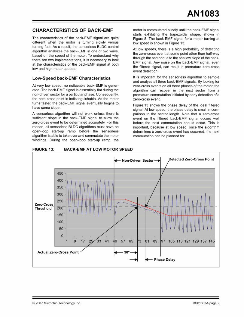
motor is commutated blindly until the back-EMF signalstarts exhibiting the trapezoidal shape, shown inFigure 8. The back-EMF signal for a motor turning atlow speed is shown in Figure 13.
At low speeds, there is a high probability of detectingthe zero-cross event at some point other than half-waythrough the sector due to the shallow slope of the back-EMF signal. Any noise on the back-EMF signal, eventhe filtered signal, can result in premature zero-crossevent detection.
It is important for the sensorless algorithm to sampleand analyze all three back-EMF signals. By looking forzero-cross events on all three phases of the motor, thealgorithm can recover in the next sector from apremature commutation initiated by early detection of azero-cross event.
Figure 13 shows the phase delay of the ideal filteredsignal. At low speed, the phase delay is small in com-parison to the sector length. Note that a zero-crossevent on the filtered back-EMF signal occurs wellbefore the next commutation should occur. This isimportant, because at low speed, once the algorithmdetermines a zero-cross event has occurred, the nextcommutation can be planned for.
FIGURE 13: BACK-EMF AT LOW MOTOR SPEED
0
50
100
150
200
250
300
350
400
450
1 9 17 25 33 41 49 57 65 73 81 89 97 105 113 121 129 137 145
Zero-Cross Threshold
30°
Non-Driven Sector
Phase Delay
Actual Zero-Cross Point
Detected Zero-Cross Point
© 2007 Microchip Technology Inc. DS01083A-page 9
AN1083
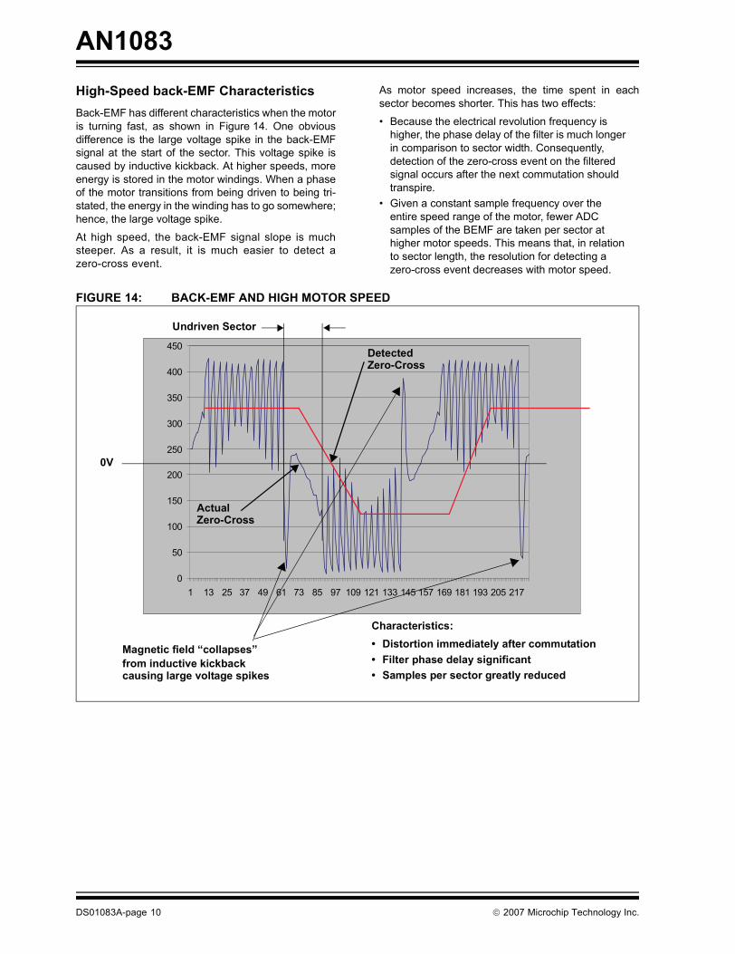
High-Speed back-EMF CharacteristicsBack-EMF has different characteristics when the motoris turning fast, as shown in Figure 14. One obviousdifference is the large voltage spike in the back-EMFsignal at the start of the sector. This voltage spike iscaused by inductive kickback. At higher speeds, moreenergy is stored in the motor windings. When a phaseof the motor transitions from being driven to being tri-stated, the energy in the winding has to go somewhere;hence, the large voltage spike.At high speed, the back-EMF signal slope is muchsteeper. As a result, it is much easier to detect azero-cross event.
As motor speed increases, the time spent in eachsector becomes shorter. This has two effects:
� Because the electrical revolution frequency is higher, the phase delay of the filter is much longer in comparison to sector width. Consequently, detection of the zero-cross event on the filtered signal occurs after the next commutation should transpire.
� Given a constant sample frequency over the entire speed range of the motor, fewer ADC samples of the BEMF are taken per sector at higher motor speeds. This means that, in relation to sector length, the resolution for detecting a zero-cross event decreases with motor speed.
FIGURE 14: BACK-EMF AND HIGH MOTOR SPEED
0
50
100
150
200
250
300
350
400
450
1 13 25 37 49 61 73 85 97 109 121 133 145 157 169 181 193 205 217
Magnetic field �collapses�
0V
Characteristics:� Distortion immediately after commutation� Filter phase delay significant� Samples per sector greatly reduced
from inductive kickback
Undriven Sector
causing large voltage spikes
ActualZero-Cross
DetectedZero-Cross
DS01083A-page 10 © 2007 Microchip Technology Inc.
AN1083
SENSORLESS IMPLEMENTATIONBased on the characteristics of back-EMF at low andhigh motor speeds, two implementations were createdto optimize both low-speed and high-speed perfor-mance of the sensorless algorithm. Transition fromthe low-speed to the high-speed implementation (andvice versa) is seamless and has built-in hysteresis. Asmotor speed increases, the transition from the low-speed to the high-speed implementation occurs at300 electrical revolutions per second by default. Asmotor speed decreases, the transition from the high-speed to the low-speed implementation occurs at200 electrical revolutions per second by default. Thetransition speed is configurable by the user (see the�Tuning Procedure� section for more information).
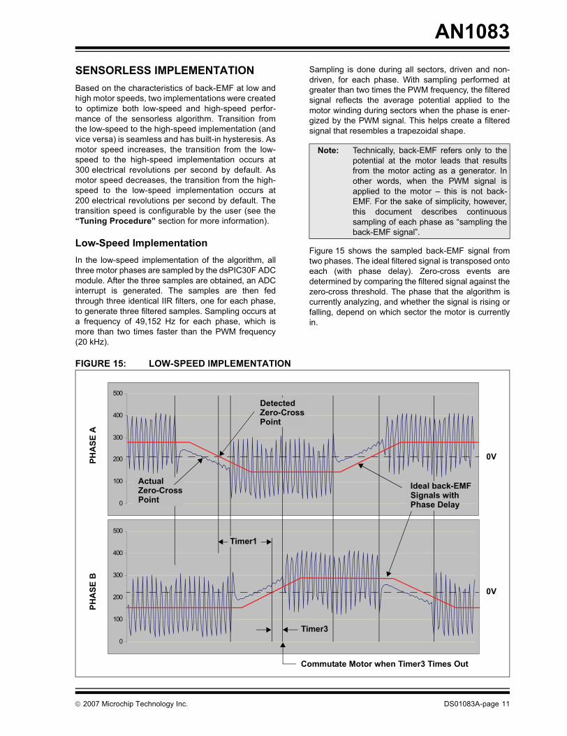
Low-Speed ImplementationIn the low-speed implementation of the algorithm, allthree motor phases are sampled by the dsPIC30F ADCmodule. After the three samples are obtained, an ADCinterrupt is generated. The samples are then fedthrough three identical IIR filters, one for each phase,to generate three filtered samples. Sampling occurs ata frequency of 49,152 Hz for each phase, which ismore than two times faster than the PWM frequency(20 kHz).
Sampling is done during all sectors, driven and non-driven, for each phase. With sampling performed atgreater than two times the PWM frequency, the filteredsignal reflects the average potential applied to themotor winding during sectors when the phase is ener-gized by the PWM signal. This helps create a filteredsignal that resembles a trapezoidal shape.
Figure 15 shows the sampled back-EMF signal fromtwo phases. The ideal filtered signal is transposed ontoeach (with phase delay). Zero-cross events aredetermined by comparing the filtered signal against thezero-cross threshold. The phase that the algorithm iscurrently analyzing, and whether the signal is rising orfalling, depend on which sector the motor is currentlyin.
FIGURE 15: LOW-SPEED IMPLEMENTATION
Note: Technically, back-EMF refers only to thepotential at the motor leads that resultsfrom the motor acting as a generator. Inother words, when the PWM signal isapplied to the motor � this is not back-EMF. For the sake of simplicity, however,this document describes continuoussampling of each phase as �sampling theback-EMF signal�.
0
100
200
300
400
500
0
100
200
300
400
500
PHA
SE A
PHA
SE B
Timer1
Timer3
Commutate Motor when Timer3 Times Out
Detected Zero-CrossPoint
Actual Zero-CrossPoint
Ideal back-EMF Signals withPhase Delay
0V
0V
© 2007 Microchip Technology Inc. DS01083A-page 11
AN1083
The dsPIC30F digital signal controllers have fiveonboard, 16-bit timers. Timer1 is used to measure theamount of time elapsed from one zero-cross event tothe next. This time is equivalent to 60 electricaldegrees. Assuming there is no phase delay when azero-cross event is detected, the next commutationshould occur in 30 degrees. Dividing the Timer1 cap-ture value by two gives the time for 30 electricaldegrees. Theoretically, this value can be loaded intothe Timer1 Period register for another timer, referred toas the commutation timer. When the interrupt for thecommutation timer occurs, it is time to commutate themotor windings to the next state.Several sources of delay must be subtracted from the30-degree time. The first is the phase delay of thedigital filter. Using the dsPIC DSC filter design tool, thisdelay was approximated as 90 μs.
Another source of delay is the time it takes to processthe ADC interrupt. The ADC Interrupt Service Routine(ISR) executes three IIR filters before determiningwhether a zero-cross event has occurred. This processtakes approximately 1.7 μS. Each of these delays mustbe subtracted from the 30° time before it is loaded inthe Commutation Timer Period register.
Timer3 is used as the commutation timer. When a zero-cross event occurs, the Timer3 Period register isloaded with the value specified by Equation 2.
EQUATION 2: TIMER3 PERIOD FOR LOW SPEED
Where:
PR3 = Timer3 Period register value
T30 = Value computed for 30 electrical degrees
DFILT = Low-speed filter phase delay
DPROC = Low-speed ADC interrupt processing delay
DPA = Phase advance (see the �Phase Advance�section for more information)
Timer3 and the Timer3 interrupt are then enabled. Themotor windings are commutated to the next state whenthe Timer3 interrupt occurs.
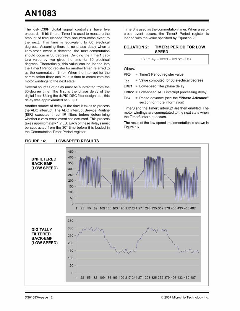
The result of the low-speed implementation is shown inFigure 16.
FIGURE 16: LOW-SPEED RESULTS
PR3 = T30 � DFILT � DPROC � DPA
0
50
100
150
200
250
300
350
400
450
1 28 55 82 109 136 163 190 217 244 271 298 325 352 379 406 433 460 487
0
50
100
150
200
250
300
350
1 28 55 82 109 136 163 190 217 244 271 298 325 352 379 406 433 460 487
UNFILTEREDBACK-EMF(LOW SPEED)
DIGITALLYFILTEREDBACK-EMF(LOW SPEED)
DS01083A-page 12 © 2007 Microchip Technology Inc.
AN1083
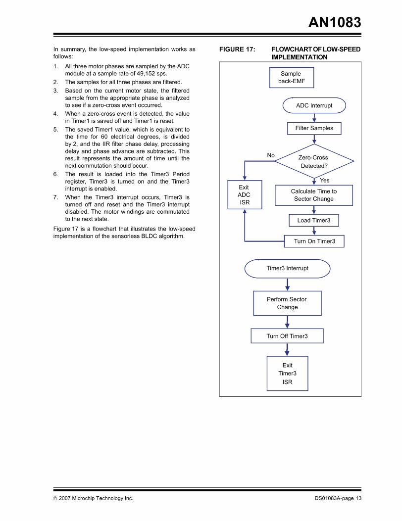
In summary, the low-speed implementation works asfollows:1. All three motor phases are sampled by the ADCmodule at a sample rate of 49,152 sps.
2. The samples for all three phases are filtered.3. Based on the current motor state, the filtered
sample from the appropriate phase is analyzedto see if a zero-cross event occurred.
4. When a zero-cross event is detected, the valuein Timer1 is saved off and Timer1 is reset.
5. The saved Timer1 value, which is equivalent tothe time for 60 electrical degrees, is dividedby 2, and the IIR filter phase delay, processingdelay and phase advance are subtracted. Thisresult represents the amount of time until thenext commutation should occur.
6. The result is loaded into the Timer3 Periodregister, Timer3 is turned on and the Timer3interrupt is enabled.
7. When the Timer3 interrupt occurs, Timer3 isturned off and reset and the Timer3 interruptdisabled. The motor windings are commutatedto the next state.
Figure 17 is a flowchart that illustrates the low-speedimplementation of the sensorless BLDC algorithm.
FIGURE 17: FLOWCHART OF LOW-SPEED IMPLEMENTATION
Sample back-EMF
ADC Interrupt
Filter Samples
Zero-Cross Detected?
Calculate Time toSector Change
Load Timer3
Turn On Timer3
Exit ADC ISR
Yes
No
Timer3 Interrupt
Perform Sector Change
Turn Off Timer3
ExitTimer3
ISR
© 2007 Microchip Technology Inc. DS01083A-page 13
AN1083
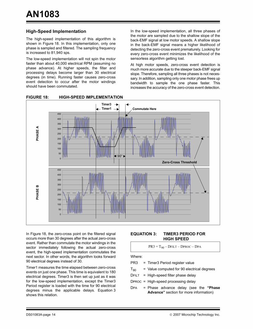
High-Speed ImplementationThe high-speed implementation of this algorithm isshown in Figure 18. In this implementation, only onephase is sampled and filtered. The sampling frequencyis increased to 81,940 sps.The low-speed implementation will not spin the motorfaster than about 40,000 electrical RPM (assuming nophase advance). At higher speeds, the filter andprocessing delays become larger than 30 electricaldegrees (in time). Running faster causes zero-crossevent detection to occur after the motor windingsshould have been commutated.
In the low-speed implementation, all three phases ofthe motor are sampled due to the shallow slope of theback-EMF signal at low motor speeds. A shallow slopein the back-EMF signal means a higher likelihood ofdetecting the zero-cross event prematurely. Looking forevery zero-cross event minimizes the likelihood of thesensorless algorithm getting lost.
At high motor speeds, zero-cross event detection ismuch more accurate due to the steeper back-EMF signalslope. Therefore, sampling all three phases is not neces-sary. In addition, sampling only one motor phase frees upbandwidth to sample the one phase faster. Thisincreases the accuracy of the zero-cross event detection.
FIGURE 18: HIGH-SPEED IMPLEMENTATION
In Figure 18, the zero-cross point on the filtered signaloccurs more than 30 degrees after the actual zero-crossevent. Rather than commutate the motor windings in thesector immediately following the actual zero-crossevent, the high-speed implementation commutates thenext sector. In other words, the algorithm looks forward90 electrical degrees instead of 30.
Timer1 measures the time elapsed between zero-crossevents on just one phase. This time is equivalent to 180electrical degrees. Timer3 is then set up just as it wasfor the low-speed implementation, except the Timer3Period register is loaded with the time for 90 electricaldegrees minus the applicable delays. Equation 3shows this relation.
EQUATION 3: TIMER3 PERIOD FOR HIGH SPEED
Where:
PR3 = Timer3 Period register value
T90 = Value computed for 90 electrical degrees
DFILT = High-speed filter phase delay
DPROC = High-speed processing delay
DPA = Phase advance delay (see the �PhaseAdvance� section for more information)
0
50
100
150
200
250
300
350
400
450
0
50
100
150
200
250
300
350
400
450
Zero-Cross Threshold
Timer1Timer3
Commutate Here
90°
PHA
SE A
PHA
SE B
PR3 = T90 � DFILT � DPROC � DPA
DS01083A-page 14 © 2007 Microchip Technology Inc.
AN1083
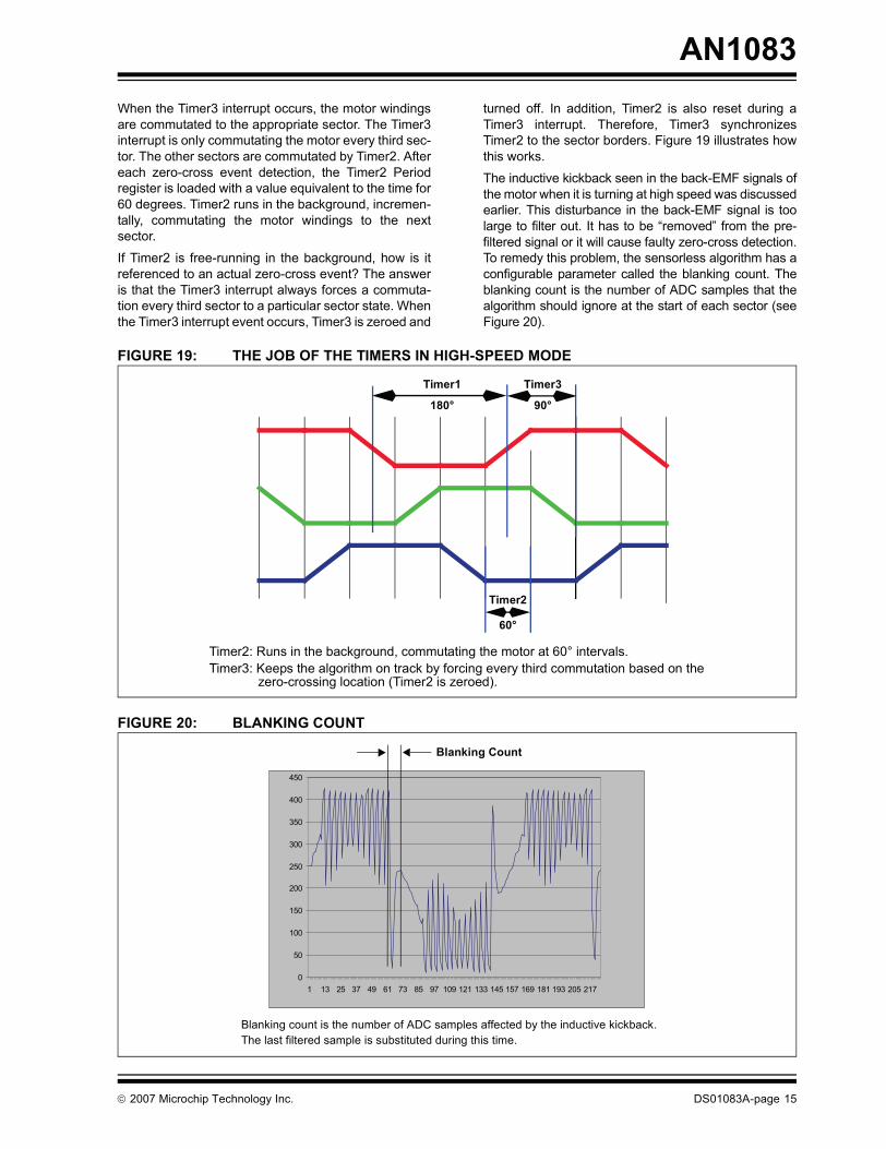
When the Timer3 interrupt occurs, the motor windingsare commutated to the appropriate sector. The Timer3interrupt is only commutating the motor every third sec-tor. The other sectors are commutated by Timer2. Aftereach zero-cross event detection, the Timer2 Periodregister is loaded with a value equivalent to the time for60 degrees. Timer2 runs in the background, incremen-tally, commutating the motor windings to the nextsector.If Timer2 is free-running in the background, how is itreferenced to an actual zero-cross event? The answeris that the Timer3 interrupt always forces a commuta-tion every third sector to a particular sector state. Whenthe Timer3 interrupt event occurs, Timer3 is zeroed and
turned off. In addition, Timer2 is also reset during aTimer3 interrupt. Therefore, Timer3 synchronizesTimer2 to the sector borders. Figure 19 illustrates howthis works.
The inductive kickback seen in the back-EMF signals ofthe motor when it is turning at high speed was discussedearlier. This disturbance in the back-EMF signal is toolarge to filter out. It has to be �removed� from the pre-filtered signal or it will cause faulty zero-cross detection.To remedy this problem, the sensorless algorithm has aconfigurable parameter called the blanking count. Theblanking count is the number of ADC samples that thealgorithm should ignore at the start of each sector (seeFigure 20).
FIGURE 19: THE JOB OF THE TIMERS IN HIGH-SPEED MODE
FIGURE 20: BLANKING COUNT
Timer1 Timer3
Timer2
Timer2: Runs in the background, commutating the motor at 60° intervals.Timer3: Keeps the algorithm on track by forcing every third commutation based on the
zero-crossing location (Timer2 is zeroed).
180° 90°
60°
0
50
100
150
200
250
300
350
400
450
1 13 25 37 49 61 73 85 97 109 121 133 145 157 169 181 193 205 217
Blanking count is the number of ADC samples affected by the inductive kickback. The last filtered sample is substituted during this time.
Blanking Count
© 2007 Microchip Technology Inc. DS01083A-page 15
AN1083
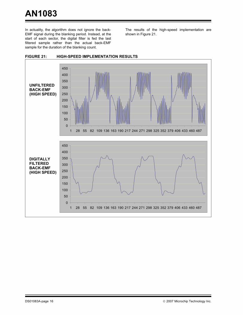
In actuality, the algorithm does not ignore the back-EMF signal during the blanking period. Instead, at thestart of each sector, the digital filter is fed the lastfiltered sample rather than the actual back-EMFsample for the duration of the blanking count.The results of the high-speed implementation areshown in Figure 21.
FIGURE 21: HIGH-SPEED IMPLEMENTATION RESULTS
UNFILTEREDBACK-EMF(HIGH SPEED)
DIGITALLYFILTEREDBACK-EMF(HIGH SPEED)
0
50
100
150
200
250
300
350
400
450
1 28 55 82 109 136 163 190 217 244 271 298 325 352 379 406 433 460 487
0
50
100
150
200
250
300
350
400
450
1 28 55 82 109 136 163 190 217 244 271 298 325 352 379 406 433 460 487
DS01083A-page 16 © 2007 Microchip Technology Inc.
AN1083
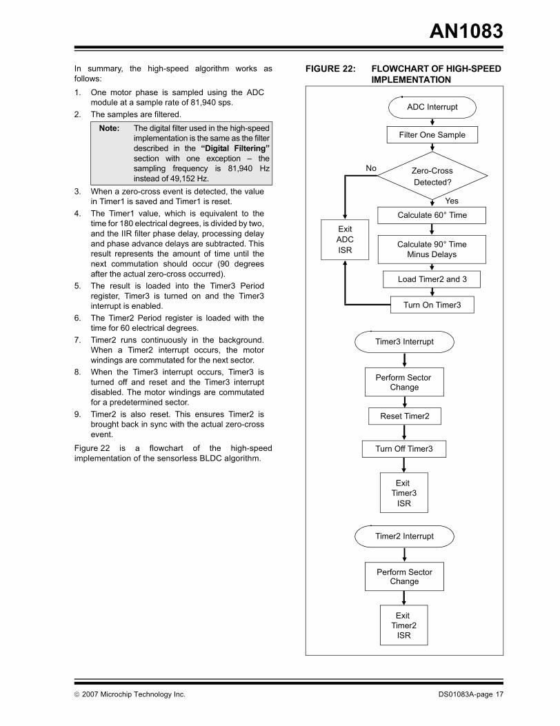
In summary, the high-speed algorithm works asfollows:1. One motor phase is sampled using the ADCmodule at a sample rate of 81,940 sps.
2. The samples are filtered.
3. When a zero-cross event is detected, the valuein Timer1 is saved and Timer1 is reset.
4. The Timer1 value, which is equivalent to thetime for 180 electrical degrees, is divided by two,and the IIR filter phase delay, processing delayand phase advance delays are subtracted. Thisresult represents the amount of time until thenext commutation should occur (90 degreesafter the actual zero-cross occurred).
5. The result is loaded into the Timer3 Periodregister, Timer3 is turned on and the Timer3interrupt is enabled.
6. The Timer2 Period register is loaded with thetime for 60 electrical degrees.
7. Timer2 runs continuously in the background.When a Timer2 interrupt occurs, the motorwindings are commutated for the next sector.
8. When the Timer3 interrupt occurs, Timer3 isturned off and reset and the Timer3 interruptdisabled. The motor windings are commutatedfor a predetermined sector.
9. Timer2 is also reset. This ensures Timer2 isbrought back in sync with the actual zero-crossevent.
Figure 22 is a flowchart of the high-speedimplementation of the sensorless BLDC algorithm.
FIGURE 22: FLOWCHART OF HIGH-SPEED IMPLEMENTATION
Note: The digital filter used in the high-speedimplementation is the same as the filterdescribed in the �Digital Filtering�section with one exception � thesampling frequency is 81,940 Hzinstead of 49,152 Hz.
ADC Interrupt
Filter One Sample
Zero-CrossDetected?
Calculate 60° Time
Load Timer2 and 3
Turn On Timer3
ExitADCISR
Yes
No
Calculate 90° TimeMinus Delays
Timer3 Interrupt
Perform Sector Change
Turn Off Timer3
Exit Timer3
ISR
Reset Timer2
Timer2 Interrupt
Perform SectorChange
Exit Timer2
ISR
© 2007 Microchip Technology Inc. DS01083A-page 17
AN1083
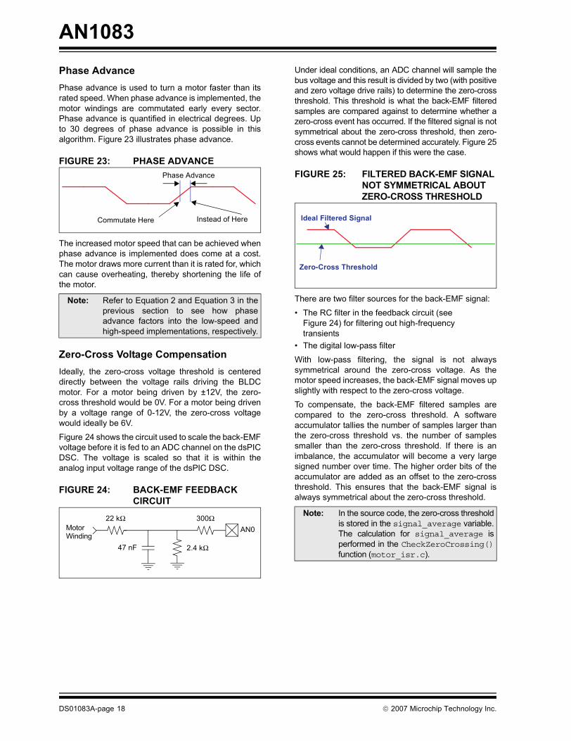
Phase AdvancePhase advance is used to turn a motor faster than itsrated speed. When phase advance is implemented, themotor windings are commutated early every sector.Phase advance is quantified in electrical degrees. Upto 30 degrees of phase advance is possible in thisalgorithm. Figure 23 illustrates phase advance.FIGURE 23: PHASE ADVANCE
The increased motor speed that can be achieved whenphase advance is implemented does come at a cost.The motor draws more current than it is rated for, whichcan cause overheating, thereby shortening the life ofthe motor.
Zero-Cross Voltage CompensationIdeally, the zero-cross voltage threshold is centereddirectly between the voltage rails driving the BLDCmotor. For a motor being driven by ±12V, the zero-cross threshold would be 0V. For a motor being drivenby a voltage range of 0-12V, the zero-cross voltagewould ideally be 6V.
Figure 24 shows the circuit used to scale the back-EMFvoltage before it is fed to an ADC channel on the dsPICDSC. The voltage is scaled so that it is within theanalog input voltage range of the dsPIC DSC.
FIGURE 24: BACK-EMF FEEDBACK CIRCUIT
Under ideal conditions, an ADC channel will sample thebus voltage and this result is divided by two (with positiveand zero voltage drive rails) to determine the zero-crossthreshold. This threshold is what the back-EMF filteredsamples are compared against to determine whether azero-cross event has occurred. If the filtered signal is notsymmetrical about the zero-cross threshold, then zero-cross events cannot be determined accurately. Figure 25shows what would happen if this were the case.
FIGURE 25: FILTERED BACK-EMF SIGNAL NOT SYMMETRICAL ABOUT ZERO-CROSS THRESHOLD
There are two filter sources for the back-EMF signal:
� The RC filter in the feedback circuit (see Figure 24) for filtering out high-frequency transients
� The digital low-pass filter
With low-pass filtering, the signal is not alwayssymmetrical around the zero-cross voltage. As themotor speed increases, the back-EMF signal moves upslightly with respect to the zero-cross voltage.
To compensate, the back-EMF filtered samples arecompared to the zero-cross threshold. A softwareaccumulator tallies the number of samples larger thanthe zero-cross threshold vs. the number of samplessmaller than the zero-cross threshold. If there is animbalance, the accumulator will become a very largesigned number over time. The higher order bits of theaccumulator are added as an offset to the zero-crossthreshold. This ensures that the back-EMF signal isalways symmetrical about the zero-cross threshold.
Note: Refer to Equation 2 and Equation 3 in theprevious section to see how phaseadvance factors into the low-speed andhigh-speed implementations, respectively.
Phase Advance
Instead of Here Commutate Here
AN0MotorWinding
22 kΩ 300Ω
47 nF 2.4 kΩ
Note: In the source code, the zero-cross thresholdis stored in the signal_average variable.The calculation for signal_average isperformed in the CheckZeroCrossing()function (motor_isr.c).
Ideal Filtered Signal
Zero-Cross Threshold
DS01083A-page 18 © 2007 Microchip Technology Inc.

AN1083
Speed ControlYou have the option of enabling a PID speed controlloop. The speed control loop is enabled via the DataMonitor and Control Interface tool. The �Tuning Proce-dure� section provides details on enabling and tuningthe PID speed control loop.The PID Speed control loop is called from theMediumEvent() function. MediumEvent() is calledevery 1 ms from the main program loop.
IMPLEMENTING THE ALGORITHMTo run the algorithm described in this application note,you must:
� Set up the hardware.� Set up the development tools and load the project
workspace in MPLAB IDE.� Tune the motor using the Data Monitor and
Control Interface (DMCI) tool.
Hardware SetupThe sensorless BLDC algorithm was developed for twohardware platforms:
� PICDEM� Low-Voltage Motor Control (MC LV) Development Board (DM183021)
� dsPICDEM� MC1 Motor Control Development Board (DM300020) in conjunction with the dsPICDEM� MC1L 3-Phase Low-Voltage Power Module (DM300022).
These development boards, along with appropriatedocumentation, are available from the Microchip website (www.microchip.com).
PICDEM� MC LV DEVELOPMENT BOARDThis development board provides a motor terminalstrip, 3-phase voltage source inverter bridge, motionsensor inputs, overcurrent protection, temperaturesensor, push button switches, nine LEDs, test points formotor current and back-EMF sensing, a speed controlpotentiometer and an RS-232 port. The board must beconfigured as shown in Table 2. The motor should beconnected as shown in Table 3.
TABLE 2: JUMPER SETTINGS FOR PICDEM� MC LV DEVELOPMENT BOARD
TABLE 3: MOTOR CONNECTIONS TO PICDEM� MC LV DEVELOPMENT BOARD
This sensorless BLDC motor control algorithm wasdeveloped to run at 30 MIPS. In order to achieve30 MIPS, the 5 MHz crystal on the PICDEM MC LVboard must be replaced with a 7.37 MHz crystal. Thisallows the algorithm to run at 29.49 MIPS.
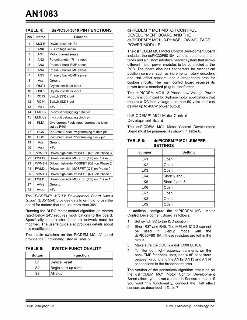
Configuring the board as described in Table 2 andTable 3 connects the dsPIC30F3010 device so that thepins on the device function as shown in Table 4. Thistable shows only the pins that are used with thisalgorithm.
Note: The PID function used in this algorithm isincluded as part of the DSP library pro-vided with Microchip�s C30 C compiler. Adetailed description of the PID functionused can be found in the �16-Bit LanguageTools Libraries� (DS51456).
Jumper Setting
J7 Short 2 and 3J8 Open
J10 ShortJ11 Short 2 and 3J12 OpenJ13 Short 2 and 3J14 OpenJ16 ShortJ17 ShortJ19 OpenJ15 Open
Label on J9 Connection
M1 Phase AM2 Phase BM3 Phase CG Ground Wire (if available)
+(1) 12-36V-(1) Ground
Note 1: Connect board/motor power and ground to J9 only if the J20 connector is not used.Refer to the �PICDEM� MC LV Develop-ment Board User�s Guide� (DS51554) for detailed information.
Note: Limited testing has shown that thealgorithm will run using the default 5 MHzcrystal (20 MIPS). Running the code usingthe 5 MHz crystal requires that the userchange the definition of FCY in general.hfrom 29490000 to 20000000.
© 2007 Microchip Technology Inc. DS01083A-page 19
AN1083
TABLE 4: dsPIC30F3010 PIN FUNCTIONSThe �PICDEM� MC LV Development Board User�sGuide� (DS51554) provides details on how to use theboard for motors that require more than 36V.
Running the BLDC motor control algorithm on motorsrated below 24V requires modifications to the board.Specifically, the resistor feedback network must bemodified. The user�s guide also provides details aboutthis modification.
The tactile switches on the PICDEM MC LV boardprovide the functionality listed in Table 5.
TABLE 5: SWITCH FUNCTIONALITY
dsPICDEM� MC1 MOTOR CONTROL DEVELOPMENT BOARD AND THE dsPICDEM� MC1L 3-PHASE LOW-VOLTAGE POWER MODULEThe dsPICDEM MC1 Motor Control Development Boardincludes the dsPIC30F6010A, various peripheral inter-faces and a custom interface header system that allowsdifferent motor power modules to be connected to thePCB. The board also has connectors for mechanicalposition sensors, such as incremental rotary encodersand Hall effect sensors, and a breadboard area forcustom circuits. The main control board receives itspower from a standard plug-in transformer.
The dsPICDEM MC1L 3-Phase Low-Voltage PowerModule is optimized for 3-phase motor applications thatrequire a DC bus voltage less than 50 volts and candeliver up to 400W power output.
dsPICDEM� MC1 Motor Control Development BoardThe dsPICDEM MC1 Motor Control DevelopmentBoard must be jumpered as shown in Table 6.
TABLE 6: dsPICDEM� MC1 JUMPER SETTINGS
In addition, configure the dsPICDEM MC1 MotorControl Development Board as follows:
1. Set switch S2 to the ICD position.2. Short R37 and R40. The MPLAB ICD 2 can not
be used in Debug mode with thedsPIC30F6010A if these resistors are left in thecircuit.
3. Make sure the DSC is a dsPIC30F6010A.4. To filter out high-frequency transients on the
back-EMF feedback lines, add 4 nF capacitorsbetween ground and the AN12, AN13 and AN14connections in the breadboard area.
The version of the sensorless algorithm that runs onthe dsPICDEM MC1 Motor Control DevelopmentBoard allows you to run a motor in Sensored mode. Ifyou want this functionality, connect the Hall effectsensors as described in Table 7.
Pin Name Function
1 MCLR Device reset via S12 AN0 Bus voltage sense3 AN1 Motor current sense4 AN2 Potentiometer (R14) input5 AN3 Phase 1 back-EMF sense6 AN4 Phase 2 back-EMF sense7 AN5 Phase 3 back-EMF sense8 VSS Ground9 OSC1 Crystal oscillator input10 OSC2 Crystal oscillator input11 RC13 Switch (S3) input12 RC14 Switch (S2) input13 VDD +5V14 EMUD2 In-circuit debugging data pin15 EMUC2 In-circuit debugging clock pin16 FLTA Overcurrent Fault input (current trip level
set by R60)17 PGD In-Circuit Serial Programming� data pin18 PGC In-Circuit Serial Programming clock pin19 VSS Ground20 VDD +5V21 PWM3H Drives high-side MOSFET (Q5) on Phase 322 PWM3L Drives low-side MOSFET (Q6) on Phase 323 PWM2H Drives high-side MOSFET (Q3) on Phase 224 PWM2L Drives low-side MOSFET (Q4) on Phase 225 PWM1H Drives high-side MOSFET (Q1) on Phase 126 PWM1L Drives low-side MOSFET (Q2) on Phase 127 AVSS Ground28 AVDD +5V
Button Function
S1 Device ResetS2 Begin start-up rampS3 All stop
Jumper Setting
LK1 OpenLK2 OpenLK3 OpenLK4 Short 2 and 3LK5 Short 2 and 3LK6 OpenLK7 OpenLK8 OpenLK9 Open
DS01083A-page 20 © 2007 Microchip Technology Inc.
AN1083
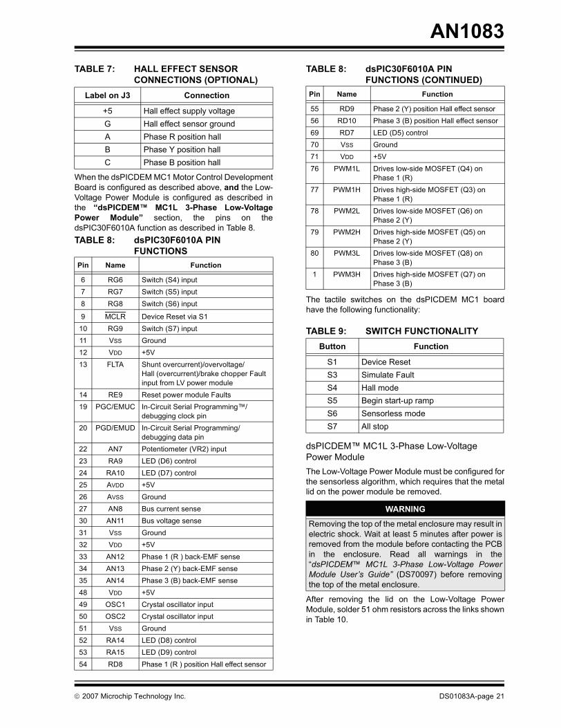
TABLE 7: HALL EFFECT SENSORCONNECTIONS (OPTIONAL)
When the dsPICDEM MC1 Motor Control DevelopmentBoard is configured as described above, and the Low-Voltage Power Module is configured as described inthe �dsPICDEM� MC1L 3-Phase Low-VoltagePower Module� section, the pins on thedsPIC30F6010A function as described in Table 8.
The tactile switches on the dsPICDEM MC1 boardhave the following functionality:
TABLE 9: SWITCH FUNCTIONALITY
dsPICDEM� MC1L 3-Phase Low-Voltage Power ModuleThe Low-Voltage Power Module must be configured forthe sensorless algorithm, which requires that the metallid on the power module be removed.
After removing the lid on the Low-Voltage PowerModule, solder 51 ohm resistors across the links shownin Table 10.
Label on J3 Connection
+5 Hall effect supply voltageG Hall effect sensor groundA Phase R position hallB Phase Y position hallC Phase B position hall
TABLE 8: dsPIC30F6010A PIN FUNCTIONS
Pin Name Function
6 RG6 Switch (S4) input7 RG7 Switch (S5) input8 RG8 Switch (S6) input
9 MCLR Device Reset via S110 RG9 Switch (S7) input11 VSS Ground12 VDD +5V13 FLTA Shunt overcurrent)/overvoltage/
Hall (overcurrent)/brake chopper Fault input from LV power module
14 RE9 Reset power module Faults19 PGC/EMUC In-Circuit Serial Programming�/
debugging clock pin20 PGD/EMUD In-Circuit Serial Programming/
debugging data pin22 AN7 Potentiometer (VR2) input23 RA9 LED (D6) control24 RA10 LED (D7) control25 AVDD +5V26 AVSS Ground27 AN8 Bus current sense30 AN11 Bus voltage sense31 VSS Ground32 VDD +5V33 AN12 Phase 1 (R ) back-EMF sense34 AN13 Phase 2 (Y) back-EMF sense35 AN14 Phase 3 (B) back-EMF sense48 VDD +5V49 OSC1 Crystal oscillator input50 OSC2 Crystal oscillator input51 VSS Ground52 RA14 LED (D8) control53 RA15 LED (D9) control54 RD8 Phase 1 (R ) position Hall effect sensor
55 RD9 Phase 2 (Y) position Hall effect sensor56 RD10 Phase 3 (B) position Hall effect sensor69 RD7 LED (D5) control70 VSS Ground71 VDD +5V76 PWM1L Drives low-side MOSFET (Q4) on
Phase 1 (R)77 PWM1H Drives high-side MOSFET (Q3) on
Phase 1 (R)78 PWM2L Drives low-side MOSFET (Q6) on
Phase 2 (Y)79 PWM2H Drives high-side MOSFET (Q5) on
Phase 2 (Y)80 PWM3L Drives low-side MOSFET (Q8) on
Phase 3 (B)1 PWM3H Drives high-side MOSFET (Q7) on
Phase 3 (B)
Button Function
S1 Device ResetS3 Simulate FaultS4 Hall modeS5 Begin start-up rampS6 Sensorless modeS7 All stop
WARNING
Removing the top of the metal enclosure may result inelectric shock. Wait at least 5 minutes after power isremoved from the module before contacting the PCBin the enclosure. Read all warnings in the�dsPICDEM� MC1L 3-Phase Low-Voltage PowerModule User�s Guide� (DS70097) before removingthe top of the metal enclosure.
TABLE 8: dsPIC30F6010A PIN FUNCTIONS (CONTINUED)
Pin Name Function
© 2007 Microchip Technology Inc. DS01083A-page 21
AN1083
TABLE 10: LINKS POPULATED WITH51 OHM RESISTORS
These are the only modifications required if the voltagesupplied to the Low-Voltage Power Module is 24V to48V.
Additional modifications are required if: (a) the suppliedvoltage is lower than 24V, or (b) a higher current levelis required. For details on making these modifications,refer to the �dsPICDEM� MC1L 3-Phase Low-VoltagePower Module User�s Guide� (DS70097).
After these modifications are made, secure the enclosurelid using the screws set aside during removal.
Table 11 lists the screw terminal connections. Makethese connections only after the lid of the Low-VoltagePower Module is securely in place.
TABLE 11: SCREW TERMINAL CONNECTIONS
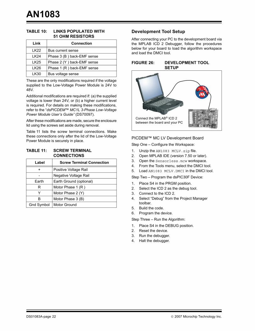
Development Tool SetupAfter connecting your PC to the development board viathe MPLAB ICD 2 Debugger, follow the proceduresbelow for your board to load the algorithm workspaceand load the DMCI tool.
FIGURE 26: DEVELOPMENT TOOL SETUP
PICDEM� MC LV Development BoardStep One � Configure the Workspace:
1. Unzip the AN1083 MCLV.zip file.2. Open MPLAB IDE (version 7.50 or later).3. Open the Sensorless.mcw workspace.4. From the Tools menu, select the DMCI tool.5. Load AN1083 MCLV.DMCI in the DMCI tool.
Step Two � Program the dsPIC30F Device:
1. Place S4 in the PRGM position.2. Select the ICD 2 as the debug tool.3. Connect to the ICD 2.4. Select �Debug� from the Project Manager
toolbar.5. Build the code.6. Program the device.
Step Three � Run the Algorithm:
1. Place S4 in the DEBUG position.2. Reset the device.3. Run the debugger.4. Halt the debugger.
Link Connection
LK22 Bus current senseLK24 Phase 3 (B ) back-EMF senseLK25 Phase 2 (Y ) back-EMF senseLK26 Phase 1 (R ) back-EMF senseLK30 Bus voltage sense
Label Screw Terminal Connection
+ Positive Voltage Rail- Negative Voltage Rail
Earth Earth Ground (optional)R Motor Phase 1 (R )Y Motor Phase 2 (Y)B Motor Phase 3 (B)
Gnd Symbol Motor Ground
Connect the MPLAB® ICD 2 between the board and your PC
DS01083A-page 22 © 2007 Microchip Technology Inc.

AN1083
dsPICDEM� MC1 MOTOR CONTROL DEVELOPMENT BOARD AND THE dsPICDEM� MC1L 3-PHASE LOW-VOLTAGE POWER MODULEStep One � Configure the Workspace:1. Unzip the AN1083 MC1.zip.2. Open MPLAB IDE (version 7.50 or later).3. Open the Sensorless.mcw workspace.4. From the Tools menu, select the DMCI tool.5. Load AN1083 MC1.DMCI in the DMCI tool.
Step Two � Program the dsPIC30F Device:
1. Place S2 in the ICD position.2. Select the ICD 2 as the debug tool.3. Connect to the ICD 2.4. Select �Debug� from the Project Manager
toolbar.5. Build the code.6. Program the device.
Step Three � Run the Algorithm:
1. Reset the device.2. Run the debugger.3. Halt the debugger.
Data Monitor and Control Interface ToolThe Data Monitor and Control Interface (DMCI) tooleliminates hours of trial and error setup by providing agraphical user interface to configure the motor param-eters. This tool is included in MPLAB IDE version 7.50or later. The DMCI tool provides sliders and text boxcontrols that let you assign global variables. You caneasily change these variables by adjusting the slidersor changing text fields. The tool also lets you assignarrays to one of four graphs.
When you have optimized the motor parameters, thegraphical interface settings (the variables assigned todifferent controls) can be saved so that other peoplehave access to the setup.
The DMCI consists of these screens and controls:
� Dynamic Data Input Screen � Dynamic Data Control Screen� Dynamic Data View Screen
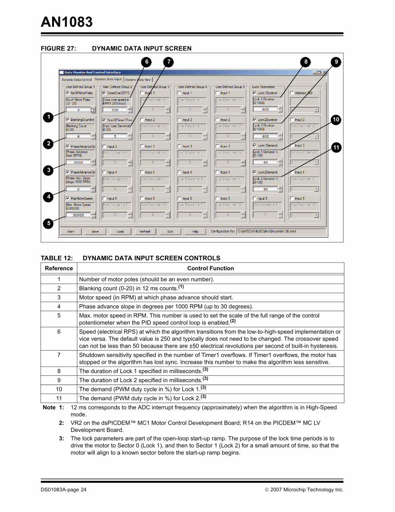
DYNAMIC DATA INPUT SCREENThe Dynamic Data Input screen (Figure 27) is used todefine the motor characteristics. Table 12 identifies thecontrols used for the sensorless algorithm.
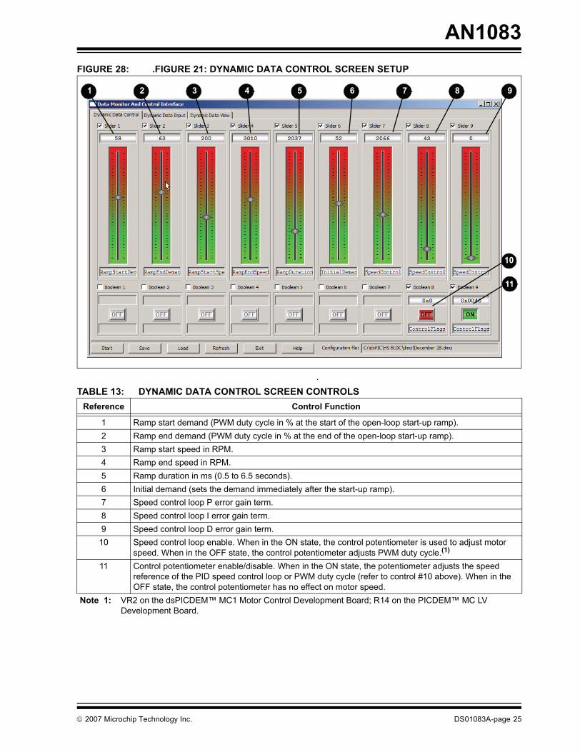
DYNAMIC DATA CONTROL SCREENThe Dynamic Data Control screen (Figure 28) is usedto set up the sensorless algorithm parameters.Table 13 identifies the controls used.
© 2007 Microchip Technology Inc. DS01083A-page 23
AN1083
FIGURE 27: DYNAMIC DATA INPUT SCREEN6 7
1
2
3
4
5
8 9
10
11
TABLE 12: DYNAMIC DATA INPUT SCREEN CONTROLSReference Control Function
1 Number of motor poles (should be an even number).2 Blanking count (0-20) in 12 ms counts.(1)
3 Motor speed (in RPM) at which phase advance should start.4 Phase advance slope in degrees per 1000 RPM (up to 30 degrees).5 Max. motor speed in RPM. This number is used to set the scale of the full range of the control
potentiometer when the PID speed control loop is enabled.(2)
6 Speed (electrical RPS) at which the algorithm transitions from the low-to-high-speed implementation or vice versa. The default value is 250 and typically does not need to be changed. The crossover speed can not be less than 50 because there are ±50 electrical revolutions per second of built-in hysteresis.
7 Shutdown sensitivity specified in the number of Timer1 overflows. If Timer1 overflows, the motor has stopped or the algorithm has lost sync. Increase this number to make the algorithm less sensitive.
8 The duration of Lock 1 specified in milliseconds.(3)
9 The duration of Lock 2 specified in milliseconds.(3)
10 The demand (PWM duty cycle in %) for Lock 1.(3)
11 The demand (PWM duty cycle in %) for Lock 2.(3)
Note 1: 12 ms corresponds to the ADC interrupt frequency (approximately) when the algorithm is in High-Speed mode.
2: VR2 on the dsPICDEM� MC1 Motor Control Development Board; R14 on the PICDEM� MC LV Development Board.
3: The lock parameters are part of the open-loop start-up ramp. The purpose of the lock time periods is to drive the motor to Sector 0 (Lock 1), and then to Sector 1 (Lock 2) for a small amount of time, so that the motor will align to a known sector before the start-up ramp begins.
DS01083A-page 24 © 2007 Microchip Technology Inc.
AN1083
FIGURE 28: .FIGURE 21: DYNAMIC DATA CONTROL SCREEN SETUP.
6 71 2 3 4 5 8 9
10
11
TABLE 13: DYNAMIC DATA CONTROL SCREEN CONTROLSReference Control Function
1 Ramp start demand (PWM duty cycle in % at the start of the open-loop start-up ramp).2 Ramp end demand (PWM duty cycle in % at the end of the open-loop start-up ramp).3 Ramp start speed in RPM.4 Ramp end speed in RPM.5 Ramp duration in ms (0.5 to 6.5 seconds).6 Initial demand (sets the demand immediately after the start-up ramp).7 Speed control loop P error gain term.8 Speed control loop I error gain term.9 Speed control loop D error gain term.
10 Speed control loop enable. When in the ON state, the control potentiometer is used to adjust motor speed. When in the OFF state, the control potentiometer adjusts PWM duty cycle.(1)
11 Control potentiometer enable/disable. When in the ON state, the potentiometer adjusts the speed reference of the PID speed control loop or PWM duty cycle (refer to control #10 above). When in the OFF state, the control potentiometer has no effect on motor speed.
Note 1: VR2 on the dsPICDEM� MC1 Motor Control Development Board; R14 on the PICDEM� MC LV Development Board.
© 2007 Microchip Technology Inc. DS01083A-page 25
AN1083
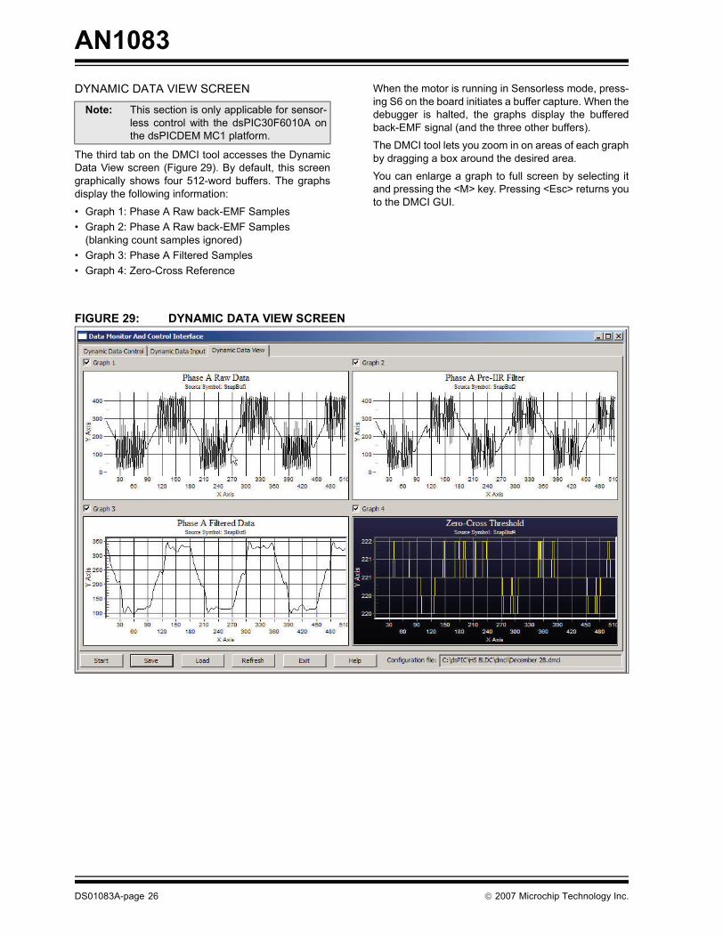
DYNAMIC DATA VIEW SCREENThe third tab on the DMCI tool accesses the DynamicData View screen (Figure 29). By default, this screengraphically shows four 512-word buffers. The graphsdisplay the following information:
� Graph 1: Phase A Raw back-EMF Samples� Graph 2: Phase A Raw back-EMF Samples
(blanking count samples ignored)� Graph 3: Phase A Filtered Samples� Graph 4: Zero-Cross Reference
When the motor is running in Sensorless mode, press-ing S6 on the board initiates a buffer capture. When thedebugger is halted, the graphs display the bufferedback-EMF signal (and the three other buffers).
The DMCI tool lets you zoom in on areas of each graphby dragging a box around the desired area.
You can enlarge a graph to full screen by selecting itand pressing the <M> key. Pressing <Esc> returns youto the DMCI GUI.
FIGURE 29: DYNAMIC DATA VIEW SCREEN
Note: This section is only applicable for sensor-less control with the dsPIC30F6010A onthe dsPICDEM MC1 platform.
DS01083A-page 26 © 2007 Microchip Technology Inc.

AN1083
Tuning ProcedureTo tune the motor parameters you must follow thisprecise process:1. Be sure the motor is stopped (failure to do so willcause a current spike when the debugger isrestarted).
2. Halt the MPLAB ICD 2 debugger.3. Change the appropriate parameter.4. Restart the MPLAB ICD 2 debugger.5. Start the motor.
This process must be repeated any time you adjust amotor parameter. Table 14 details which switches startand stop the motor for each development board.
The method used to tune the start-up ramp and PIDspeed control parameters follows these basic steps:1. Set up the initial parameters that match the
characteristics of the motor.2. Initialize the open-loop start-up ramp.3. Tune the open-loop start-up parameters.4. Tune the speed control loop.
Follow these detailed procedures:
Step One: Set up the initial parameters that match thecharacteristics of the motor.
1. On the Dynamic Data Input screen, enter thenumber of motor poles and maximum speed ofthe motor. Leave the blanking count at thedefault value.
2. Disable phase advance during the initial tuningof motor parameters by setting the phaseadvance start speed to an RPM value that ishigher than the maximum motor speed.
3. Set the phase advance slope to zero. Thisensures that no phase advance is added duringthe initial tuning process.
4. The crossover speed should be 250. If you havea lower speed motor (40k electrical RPMmaximum) that does not require phaseadvance, you can change this to a very highnumber, such as 700, to make sure thealgorithm runs in Low-Speed mode all the time.
5. Enter 20 for the shutdown sensitivity. Thismakes the algorithm less sensitive to shutdowndetection (the lower this number the moresensitive the algorithm).
Step Two: Initialize the open-loop start-up ramp.
1. Set the Lock 1 and Lock 2 duration values at600 ms.
2. Set the lock demands. It is best to start out atlower demand values. Start at a lock value of 10for Lock 1 and Lock 2. Increase the Lock 1 andLock 2 demands until the motor snaps to thelock positions, but it is not drawing sufficient cur-rent to damage the motor windings or the drivecircuitry. The whole purpose of the lock positionsis to bring the motor to a known sector beforebeginning the start-up ramp.
3. The remaining start-up ramp parameters arefound on the Dynamic Data Control screen. Inthe lower right hand corner of this screen, dis-able the speed control loop and the controlpotentiometer by setting the enabled booleanbuttons to �off�. The idea is to get the sensorlessalgorithm to run the motor before the algorithmhas to compensate for changes in demand.
4. Set the ramp duration to the full duration �6500 ms. Once the start-up ramp is tuned sothat motor start-up is successful, the rampduration can be reduced.
Step Three: Tune the open-loop start-up parameters.
1. Ignore the PID gain sliders for the moment.Concentrate on getting the ramp start speed,end speed, start demand and end demand setso the that motor spins fast enough for thesensorless algorithm to sync up.
2. Use the sliders on the Dynamic Data Controlscreen to set the start and end speeds. Set theend speed to something on the order of 12-20%of full motor speed.
For motors with a lot of inertia and/or manymotor poles, the start speed will have to be lessthan 100 RPM. For motors with little inertia and/or few motor poles, the start speed can behigher (typically between 200 and 300 RPM).
3. Keep the start, end and initial demand slidersthe same. Set all three parameters to the samedemand value specified for Lock 1 and Lock 2.
Click �start� on the DMCI tool, then press thebutton on the board that initializes the start-upramp (this is hardware platform dependant).
If the motor sits in place and shutters, moredemand is needed. Press the button on theboard to stop the motor. Click �halt� on the DMCItool. Increase the start, end and initial demandby units of 5 and repeat this step until the motorstarts.
TABLE 14: MOTOR CONTROL SWITCHESDevelopment Board Type On Off
dsPICDEM� MC1 S5 S7PICDEM� MC LV S2 S3
Note: You should increase demand slowly. If youjump directly to a large demand value, themotor will draw a lot of current which couldharm the motor or drive circuitry.
© 2007 Microchip Technology Inc. DS01083A-page 27

AN1083
4. The motor should now start turning when themotor start button is pressed. If motor commuta-tions appear to occur faster than the motor cankeep up with, increase the end and initialdemands.
The end demand should never be greater than20% higher than the start demand. Typically, theinitial demand should be slightly lower than theend demand. If the motor still appears to �slip�,decrease the end speed.
5. The motor should now spin up, and the sensor-less algorithm should take over at the end of thestart-up ramp. Fine tune the ramp parametersuntil motor start-up is reliable.
6. Experiment with decreasing the ramp duration.Find the minimum value of the ramp durationthat will still allow the motor to start-up reliably.
7. It is now time to enable the control potentiometer.Enable the control potentiometer on the DMCItool.
Do not enable speed control. The potentiometerposition will correlate to the PWM duty cycle; fullclockwise is 100% duty cycle.
Estimate the potentiometer position that corre-sponds to the initial demand value. Set thepotentiometer in this position and initiate thestart-up ramp. If the motor doesn�t start, adjustthe potentiometer and try again. When the motordoes run, the speed is adjustable by turning thepotentiometer.
Step Four: Tune speed control loop.
1. The speed control loop can now be enabled.Enable the speed control loop on the DMCI inter-face. The potentiometer position now correlatesto motor speed (in RPM). Full clockwise corre-sponds to the maximum motor speed specified onthe Dynamic Data Input screen of the DMCI tool.
2. Move the initial demand slider to about 80% of theend demand. Then, zero the integral andderivative terms and center the proportional slider.
Estimate the potentiometer position thatcorresponds to the end speed of the start-upramp. Try running the motor. Adjust the controlpotentiometer and the P term until the motorstarts successfully. (Lowering the initial startdemand can help improve start-up perfor-mance.) Some Integral gain may be needed tostart the motor successfully.
3. Tune the P, I and D terms until the desired motorperformance is obtained. Very little integral term isneeded in comparison to the proportional term.
See the �Troubleshooting� section for tips on possibleproblem solutions.
Changing the Digital Filter CoefficientsThe low and high-speed filter coefficients are located inBEMF_filter.s. These filter coefficients can bereplaced by new coefficients generated by the dsPICDSC Filter Design tool.
Other Tunable Features of the AlgorithmTable 15 lists some of the configurable #define statementsand where they are located in the source code.
TABLE 15: OTHER CONFIGURABLE PARAMETERS.
Note: Altering these features is not recom-mended. Adjust these features at yourown risk.
Parameter Defined In Description
FCY general.h The processor frequency in instructions per second.FPWM general.h PWM frequency.FULL_DUTY general.h The PWM period (a function of FCY and FPWM).FILTER_PHASE_DELAY general.h Filter phase delay in Timer3 counts.PROCESSING_DELAY general.h ADC interrupt processing delay in Timer3 counts for Low-Speed mode. PROCESSING_DELAY_HS general.h ADC interrupt processing delay in Timer3 counts for High-Speed mode. CYCLE_BY_CYCLE_PROTECTIONFAULT_CAUSE_PWM_SHUTDOWNNO_FAULT_PROTECTION
pwm.c Three choices for what the PWM module will do when a Fault condition occurs. Change the �FLTACON =� to one of these choices.
DEAD_TIME pwm.c PWM dead time in seconds.SNAPSHOT snapshot.h When defined RAM is allocated for the Dynamic Data View graphs.SNAPSIZE snapshot.h The size of the four snapshot buffers in bytes.
DS01083A-page 28 © 2007 Microchip Technology Inc.

AN1083
CONCLUSIONThis application note is intended for the developer whowants to drive a sensorless BLDC motor without theuse of discrete, low-pass filtering hardware and off-chipcomparators.
The algorithm described uses digital filtering of theback-EMF signals generated by a turning BLDC motor.Digital filtering makes it possible to more accuratelydetect the zero-cross events in the back-EMF signal.When detected by the dsPIC DSC, zero-cross eventsprovide the information needed by the algorithm tocommutate the motor windings
Accurately detecting the zero-cross events in a back-EMF signal is the key to sensorless control of a BLDCmotor that is driven using six-step, or trapezoidal,commutation. The use of digital filtering, as opposed tohardware filters or external comparators, requires lesshardware, which equates to less cost and a smallerPCB. The use of an open source solution equates to ashorter development cycle
Finally, the Microchip development tools that supportthe dsPIC DSC device family, and specifically, the DataMonitor and Control Interface tool included withMPLAB IDE version 7.50 or later, allow the algorithm tobe quickly adapted to your specific motor andapplication.
RESOURCESFor BLDC motor control, see:
� AN901, �Using the dsPIC30F for Sensorless BLDC Control�
� AN957, �Sensored BLDC Motor Control Using dsPIC30F2010�
� AN1017, �Sinusoidal Control of PMSM Motors with dsPIC30F DSC�
� AN1078, �Sensorless Field Oriented Control of PMSM Motors�
For information on the hardware platforms compatiblewith this algorithm, see:
� �dsPICDEM� MC1 Motor Control Development Board User�s Guide� (DS70098)
� �dsPICDEM� MC1L 3-Phase Low-Voltage Power Module User�s Guide� (DS70097)
� �PICDEM� MC LV Development Board User�s Guide� (DS51554)
For information on the PID algorithm, see:
� �16-Bit Language Tools Libraries� (DS51456)
© 2007 Microchip Technology Inc. DS01083A-page 29
AN1083
TROUBLESHOOTINGProblem: The motor ramps up and then, at mid tohigh-speed, it just quits.
Possible Solution: Try (a) increasing the blankingcount; (b) if you have a lower speed motor (maximumspeed much lower than 90,000 electrical RPM) and youare adding a lot of phase advance, you may need to havethe algorithm transition from the low-speed implementa-tion to the high-speed implementation earlier. Adjust thecrossover point lower (from 250 to 200, then to 150).Decreasing the phase advance slope may also help.
Problem: The back-EMF from my motor does not looktrapezoidal at all on the oscilloscope.
Possible Solution: This algorithm requires a trapezoidalshape to the motor�s back-EMF signal. AN1078, �Sen-sorless Field Oriented Control of PMSM Motors� explainshow to run a sinusoidal motor in Sensorless mode.
Problem: When running the code, an oscillator trapoccurs.
Possible Solution: After programming the device withthe debugger, make sure you reset the MPLAB ICD 2.
Problem: The MPLAB ICD 2 will not debug/programthe device (when using the PICDEM MC LV board).
Possible Solution: Make sure S4 is in the PRGMposition when programming the device. Switch S4 tothe DEBUG position once the device is programmedand before debugging.
Problem: How do I know how fast the motor is going.
Possible Solution: Select �Watch� from the Viewmenu in MPLAB ICD 2. This brings up the Watch win-dow. Enter the variable �Speed� in the Watch window.Run the motor using the algorithm. When the motor isat the desired speed, press the �motor off� button. Haltthe ICD 2. The speed of the motor at the time the�motor off� button was pressed will be displayed (inRPM) in the Watch window.
Problem: The motor you are using does not need torun faster than 40,000 electrical RPM and phaseadvance is not required.
Possible Solution: Set the crossover frequency to themaximum allowable value � 900 electrical revolutionsper second. This will insure the motor only runs in Low-Speed mode. High-Speed mode is not necessary formotors that run slower than 40,000 electrical RPM. Thenumber, 40,000 electrical RPM, was arrived at byadding up the processing and filter phase delays. Themaximum amount of delay that can occur in Low-Speed mode is 30 electrical degrees. When the delaysare added up (assuming no phase advance) and setequal to 30 electrical degrees, the fastest electricalspeed is calculated to be around 48,000 RPM.
Problem: The motor stops running right after the start-up ramp. It seems like it should have enough speed tostart.
Possible Solution: When first tuning the start-upramp, make sure the potentiometer input and speedcontrol loop are disabled. These can be disabled by theboolean controls on the Dynamic Data Control screenof the DMCI tool.
Problem: How do I know if the motor is running inHigh-Speed mode or not?
Possible Solution: Add the bit array, �ControlFlags�,to the Watch window. The High-Speed mode bit is setwhen the motor is running in High-Speed mode. The bitis clear when the motor is in Low-Speed mode. You willhave to halt the ICD 2 when the motor is running tocheck this bit.
Alternatively, check LED D5 if using the MC1 board �this LED is on when the motor is in High-Speed mode.
Problem: When I add phase advance, the motor doesnot cross over to High-Speed mode.
Possible Solution: Too much phase advance whenthe motor is running in Low-Speed mode will cause themotor to run improperly. Set the phase advance startfrequency past the crossover frequency. The crossoverfrequency is in electrical revolutions per second. Toconvert to RPM, add 50 to the crossover frequency,multiply by 60 and divide by the number of pole pairs.
Problem: When using the MC1 board, I always get anoscillator trap when I first try to run the ICD 2 after Iprogram the dsPIC30F6010A.
Possible Solution: After the dsPIC30F6010A is pro-grammed, reset the ICD 2. Then, run the ICD 2 and haltthe ICD 2. Next, click �run� on the DMCI tool. If anothertrap occurs, you will have to go through the sequencejust described to clear the trap and load the parametersin the DMCI tool into the device.
Problem: I change the position of the sliders in theDMCI tool and it appears like the parameters are notupdated in the dsPIC DSC.
Possible Solution: First, the DMCI tool is not a real-time tool (at the time of this writing). In order forchanges you make to parameters to be loaded into thedsPIC DSC, you will have to halt the ICD 2, make thedesired change to a parameter and restart the ICD 2.
Secondly, make sure the code is not stuck in a trap. Tocheck to see whether the device is in a trap, halt theICD 2 and look at the trap.c file. If the PC counterarrow (green arrow) is located in that file, then a traphas occurred. Clear the trap by resetting the ICD 2 andchecking for other Fault sources.
DS01083A-page 30 © 2007 Microchip Technology Inc.
AN1083
Problem: How do I know how fast my motor is running?Possible Solution: Add the �Speed� variable to theWatch window. When the motor is at speed, press thetactile switch that stops the motor. Halt the ICD 2. TheWatch window will display the speed of the motor at thetime you stopped the motor.
Problem: I am measuring the speed of the motor usinga handheld tachometer. The value in �Speed� does notmatch my measured speed.
Possible Solution: Assuming the handheld tachometeris correct, make sure that the processor is running at theinstruction cycle rate specified by FCY in general.h. Inother words, if the processor is running at 30 MIPS andFCY is specified as 20000000, then the calculated motorspeed will not be accurate.
Problem: I get an oscillator trap.
Possible Solution: After programming the device,reset the device before running the debugger.
Problem: Why do I have to run, and then halt thedebugger once, before any adjustments to the motortuning parameters in the DMCI tool will take effect?
Possible Solution: The motor start-up parameters areinitialized in the source code. When you first run thedebugger, the start-up parameters are initialized tothe values specified in the source code (seeTuningInterface.c). You must run the codebeyond the initialization point for these parameters andthen any adjustments you make to these parameters,using the DMCI tool, will take effect. The motor tuningparameters are initialized in the source code so thatwhen you are finished tuning the motor, you can �hardcode� the tuned parameters into the code and programthe device.
© 2007 Microchip Technology Inc. DS01083A-page 31

AN1083
NOTES:DS01083A-page 32 © 2007 Microchip Technology Inc.

Note the following details of the code protection feature on Microchip devices:� Microchip products meet the specification contained in their particular Microchip Data Sheet.
� Microchip believes that its family of products is one of the most secure families of its kind on the market today, when used in the intended manner and under normal conditions.
� There are dishonest and possibly illegal methods used to breach the code protection feature. All of these methods, to our knowledge, require using the Microchip products in a manner outside the operating specifications contained in Microchip�s Data Sheets. Most likely, the person doing so is engaged in theft of intellectual property.
� Microchip is willing to work with the customer who is concerned about the integrity of their code.
� Neither Microchip nor any other semiconductor manufacturer can guarantee the security of their code. Code protection does not mean that we are guaranteeing the product as �unbreakable.�
Code protection is constantly evolving. We at Microchip are committed to continuously improving the code protection features of ourproducts. Attempts to break Microchip�s code protection feature may be a violation of the Digital Millennium Copyright Act. If such actsallow unauthorized access to your software or other copyrighted work, you may have a right to sue for relief under that Act.
Information contained in this publication regarding deviceapplications and the like is provided only for your convenienceand may be superseded by updates. It is your responsibility toensure that your application meets with your specifications.MICROCHIP MAKES NO REPRESENTATIONS ORWARRANTIES OF ANY KIND WHETHER EXPRESS ORIMPLIED, WRITTEN OR ORAL, STATUTORY OROTHERWISE, RELATED TO THE INFORMATION,INCLUDING BUT NOT LIMITED TO ITS CONDITION,QUALITY, PERFORMANCE, MERCHANTABILITY ORFITNESS FOR PURPOSE. Microchip disclaims all liabilityarising from this information and its use. Use of Microchipdevices in life support and/or safety applications is entirely atthe buyer�s risk, and the buyer agrees to defend, indemnify andhold harmless Microchip from any and all damages, claims,suits, or expenses resulting from such use. No licenses areconveyed, implicitly or otherwise, under any Microchipintellectual property rights.
© 2007 Microchip Technology Inc.
Trademarks
The Microchip name and logo, the Microchip logo, Accuron, dsPIC, KEELOQ, KEELOQ logo, microID, MPLAB, PIC, PICmicro, PICSTART, PRO MATE, PowerSmart, rfPIC, and SmartShunt are registered trademarks of Microchip Technology Incorporated in the U.S.A. and other countries.
AmpLab, FilterLab, Linear Active Thermistor, Migratable Memory, MXDEV, MXLAB, PS logo, SEEVAL, SmartSensor and The Embedded Control Solutions Company are registered trademarks of Microchip Technology Incorporated in the U.S.A.
Analog-for-the-Digital Age, Application Maestro, CodeGuard, dsPICDEM, dsPICDEM.net, dsPICworks, ECAN, ECONOMONITOR, FanSense, FlexROM, fuzzyLAB, In-Circuit Serial Programming, ICSP, ICEPIC, Mindi, MiWi, MPASM, MPLAB Certified logo, MPLIB, MPLINK, PICkit, PICDEM, PICDEM.net, PICLAB, PICtail, PowerCal, PowerInfo, PowerMate, PowerTool, REAL ICE, rfLAB, rfPICDEM, Select Mode, Smart Serial, SmartTel, Total Endurance, UNI/O, WiperLock and ZENA are trademarks of Microchip Technology Incorporated in the U.S.A. and other countries.
SQTP is a service mark of Microchip Technology Incorporated in the U.S.A.
All other trademarks mentioned herein are property of their respective companies.
© 2007, Microchip Technology Incorporated, Printed in the U.S.A., All Rights Reserved.
Printed on recycled paper.
DS01083A-page 33
Microchip received ISO/TS-16949:2002 certification for its worldwide headquarters, design and wafer fabrication facilities in Chandler and Tempe, Arizona, Gresham, Oregon and Mountain View, California. The Company�s quality system processes and procedures are for its PIC®
MCUs and dsPIC® DSCs, KEELOQ® code hopping devices, Serial EEPROMs, microperipherals, nonvolatile memory and analog products. In addition, Microchip�s quality system for the design and manufacture of development systems is ISO 9001:2000 certified.

DS01083A-page 34 © 2007 Microchip Technology Inc.
AMERICASCorporate Office2355 West Chandler Blvd.Chandler, AZ 85224-6199Tel: 480-792-7200 Fax: 480-792-7277Technical Support: http://support.microchip.comWeb Address: www.microchip.comAtlantaDuluth, GA Tel: 678-957-9614 Fax: 678-957-1455BostonWestborough, MA Tel: 774-760-0087 Fax: 774-760-0088ChicagoItasca, IL Tel: 630-285-0071 Fax: 630-285-0075DallasAddison, TX Tel: 972-818-7423 Fax: 972-818-2924DetroitFarmington Hills, MI Tel: 248-538-2250Fax: 248-538-2260KokomoKokomo, IN Tel: 765-864-8360Fax: 765-864-8387Los AngelesMission Viejo, CA Tel: 949-462-9523 Fax: 949-462-9608Santa ClaraSanta Clara, CA Tel: 408-961-6444Fax: 408-961-6445TorontoMississauga, Ontario, CanadaTel: 905-673-0699 Fax: 905-673-6509
ASIA/PACIFICAsia Pacific OfficeSuites 3707-14, 37th FloorTower 6, The GatewayHabour City, KowloonHong KongTel: 852-2401-1200Fax: 852-2401-3431Australia - SydneyTel: 61-2-9868-6733Fax: 61-2-9868-6755China - BeijingTel: 86-10-8528-2100 Fax: 86-10-8528-2104China - ChengduTel: 86-28-8665-5511Fax: 86-28-8665-7889China - FuzhouTel: 86-591-8750-3506 Fax: 86-591-8750-3521China - Hong Kong SARTel: 852-2401-1200 Fax: 852-2401-3431China - QingdaoTel: 86-532-8502-7355Fax: 86-532-8502-7205China - ShanghaiTel: 86-21-5407-5533 Fax: 86-21-5407-5066China - ShenyangTel: 86-24-2334-2829Fax: 86-24-2334-2393China - ShenzhenTel: 86-755-8203-2660 Fax: 86-755-8203-1760China - ShundeTel: 86-757-2839-5507 Fax: 86-757-2839-5571China - WuhanTel: 86-27-5980-5300Fax: 86-27-5980-5118China - XianTel: 86-29-8833-7250Fax: 86-29-8833-7256
ASIA/PACIFICIndia - BangaloreTel: 91-80-4182-8400 Fax: 91-80-4182-8422India - New DelhiTel: 91-11-4160-8631Fax: 91-11-4160-8632India - PuneTel: 91-20-2566-1512Fax: 91-20-2566-1513Japan - YokohamaTel: 81-45-471- 6166 Fax: 81-45-471-6122Korea - GumiTel: 82-54-473-4301Fax: 82-54-473-4302Korea - SeoulTel: 82-2-554-7200Fax: 82-2-558-5932 or 82-2-558-5934Malaysia - PenangTel: 60-4-646-8870Fax: 60-4-646-5086Philippines - ManilaTel: 63-2-634-9065Fax: 63-2-634-9069SingaporeTel: 65-6334-8870Fax: 65-6334-8850Taiwan - Hsin ChuTel: 886-3-572-9526Fax: 886-3-572-6459Taiwan - KaohsiungTel: 886-7-536-4818Fax: 886-7-536-4803Taiwan - TaipeiTel: 886-2-2500-6610 Fax: 886-2-2508-0102Thailand - BangkokTel: 66-2-694-1351Fax: 66-2-694-1350
EUROPEAustria - WelsTel: 43-7242-2244-39Fax: 43-7242-2244-393Denmark - CopenhagenTel: 45-4450-2828 Fax: 45-4485-2829France - ParisTel: 33-1-69-53-63-20 Fax: 33-1-69-30-90-79Germany - MunichTel: 49-89-627-144-0 Fax: 49-89-627-144-44Italy - Milan Tel: 39-0331-742611 Fax: 39-0331-466781Netherlands - DrunenTel: 31-416-690399 Fax: 31-416-690340Spain - MadridTel: 34-91-708-08-90Fax: 34-91-708-08-91UK - WokinghamTel: 44-118-921-5869Fax: 44-118-921-5820
WORLDWIDE SALES AND SERVICE
12/08/06
Related Documents