An &Bit, 1-Gsampleh Folding-Interpolating Analog-to-Digital Converter bs Wei An A thesis submitted in conforxnity with the requirements for the degree of Master of Applied Science Department of Electrical and Cornputer Engineering University of Toronto 2000 O Copyright by Wei An 2000

Welcome message from author
This document is posted to help you gain knowledge. Please leave a comment to let me know what you think about it! Share it to your friends and learn new things together.
Transcript
An &Bit, 1-Gsampleh Folding-Interpolating
Analog-to-Digital Converter
bs Wei An
A thesis submitted in conforxnity with the requirements for the degree of Master of Applied Science
Department of Electrical and Cornputer Engineering University of Toronto
2000
O Copyright by Wei An 2000

The author has graPted a non- exclusive licence allowhg the National Library of Canada to reproduce, loan, distn'bute or sel1 copies of this thesis m microform, paper or electronic formats.
The author ntaiiis ownaship of the copyright in this dusis. Neither the thesis nor sub- extracts b m it may be printed or otherwise reproduced without the author's
L'autaa a accord6 me licence non
Biblioth&que nationale du Canada de reproduire, prêter, distn'buer ou vendre des copies de cette thése sous la fonne de microiiche/film, & reproduction sur papier ou sur format électronique.
L'auteur caasave la propriété du droit d'auteur qui protège cette thèse. Ni la t h h ni des extraits substantieîs de celle-ci ne doivent être imprimés ou autrement reproduits sans son
An 8=Bit, l&le/s Folding-Interpolating Analog-to- Digitai Converter
Master of Applied Science, 2ûûû
Wei An
Department of Electricai and Cornputer Engineering University of Toronto
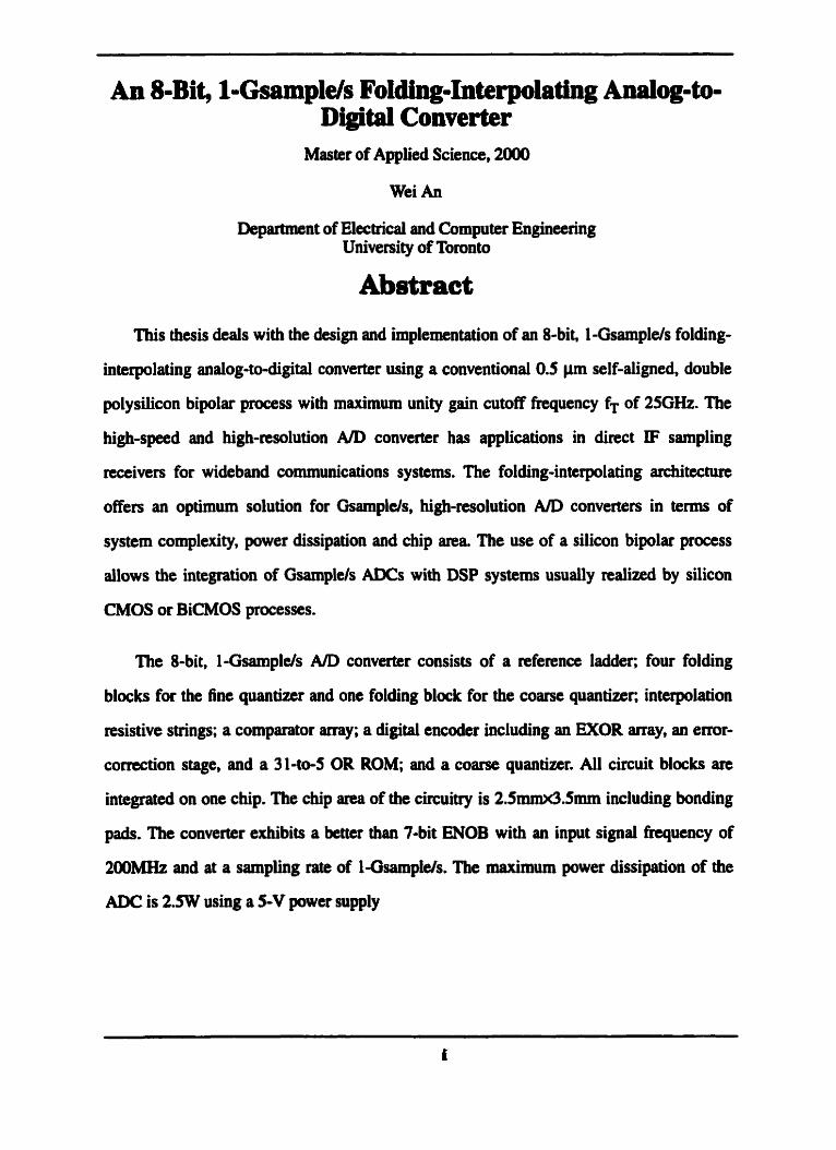
This thesis deals with the design and implementation of an 8-bit, 1-Gsampleh folding-
interpolating analog-to-digital converter using a conventional 0.5 pn self-aligned, double
polysilicon bipolar process with maximum unity gain cutoff frequency fT of 25GHz. The
high-spad and high-resolution AID converter has applications in direct IF sampling
receivers for wideband communications systems. The folding-interpolating architecture
offers an optimum solution for Gsamplcls. hi&-cesolution AID converters in tenns of
system complexity, power dissipation and cbip ana The use of a silicon bipolar process
aiiows the integration of Gsampleh ADCs with DSP systems usually realized by silicon
CMOS or BiCMOS processes.
The 8-bit, I-Gsample/s A/D converter consists of a refennce ladder; four folding
blocks for the fine quantizer and one folding block for the coarse quantizer. interpolation
resistive strings; a comparator array; a digital encoder including an EXOR -y, an em>r-
correction stage. and a 3 1-to-5 OR ROM; and a coarse quantber. Ail circuit blocks arc
integratd on one chip. The chip ana of the circuitry is 2.5mmx3.5mm including bonding
pads. The converter exhibits a better than Fbit ENOB with an input signai frcquency of
2ûûMHz and at a sampling rate of l-Osamplels. The maximum power dissipation of the
AM3 is 2.5W using a 5-V power supply

1 would Wre to expms my sincm gratitude to Professor C.A.T. Salama for bis
insightfd guidance and invaluable assistance throughout the course of this work.
1 also would Iüre to th& Pmfessor John Long, Rofessor Wai k g Ng, Rofessor
Khoman Phang for theh technical advice and help.
1 am indebted to N i g Ge for the countless hours of valuable discussion both
technicaüy and persondy.
My sincere thanks to Jar0 Ristupa for his seamless technical supports. My appreciation
goes to Hormoz Djahanshahi for his help during the chip testing. My appreciation also
extends to al1 the staE and students in the Micrae1ectron.i~ Research Laboratory including
Richard Barber, Dana Reem, Anthoula Kampouris, Mikna Khazak, Dod Chettiar, Jeewika
Ranaweera, Mehrdad Ramezani, Dusan Suvakovic, Rick Kubowicz, John Ren, Farbang
Vessal, Sotoudeh Hamedi-Hagh, TakayuLi Hayashi, Stanley Ma for al1 their help.
1 wouid like to thank my fiiend, Song Ye, who kept me cornpany with his constructive
discussions and cheemil chats, and the rest of my fricnds: Jianghong Hu, Yucai Zhang,
Sean Phang, Louis Zhang, Shuo Chen, Polly Tang, Franklin Zhao, W a n Jiao who were
always then for me.
A special word of th& to my parents and my sisters who have been a constant source
of support and encouragement.
And to my husband Heng, thank you for your patience, support and love. To my
daughter Dian, for king the best baby a mother could have.
This work was supprted by Mimaet, Gcnnum. Mitel, Norte1 Networks, and PMC-
Sierra.

Table of Contents
1.1 A/D Converter Characteristics and Architectms ................................. ...............3
1.1.1 A/D Converter Characteristics .............................................. .......,,..... 3
1.1.2 ND Converter Architectums .......................... ..,... ......................................... 4
1.2 Folding-Interpolating A/D converten ..................................................................... 8
1.3 M o u s Work on Folding-Interpolating Gsamplels A D converters ................... 10 1.4 Thesis Objective and ûutiine .................... .. .... ............ ....................... ...11
References
............................................................................. 2.1 Introduction ..... -16
........... 2.2 Folding-Interpolating Techniques .................... ............................... 1 9
...................................... 2.3 Block Diagram of the 8-bit Folding-Interpolating ADC 21
........................................................................ 2.4 Folding and Interpolating Block 23
2.4.1 Design of the Folding C h i t .................................................................... 23
.................................................................... 2.4.2 Interpolation .................... ... 28
............. ... 2.4.3 Refecence Ladder .......................... ...... .. ........ ... 2.5 High-Spced Comparators ................. ....... .... d
2.6 Digital Encoder for 5 Fine Bits .................... .. ..... ....C...............e ....................... 32 ............................................................... 2.7 The Co- Quantizer ............................ 36
....................................................... 2.8 System Simulation ................................. 37
2.9 Summary .................... .. .................................................................................... 40
References
3-1 htroduction ......................... ............ ....................

List of Figures
Page
Fig . 1.1. ExPmples of incnaping DSP complexity in communication systems . (a) A classic
system with analog demodulatot followed by baseband N D conversion and DSP . (b) An advanced system with IF A D conversion using digital demoddation and signal processing . (c) An emrgirig system with RF A/D convcrsion followed by digital downconversion.
demodulation . and basedband signal processing ............................................................... *2
Fig . 1.2. (a) An ideal unipolar quantizaiion operation for a ramp input. (b) quanthtion
noise .................................................................................................................................... 3
................... ...................*..*...*....*.... Fig . 1.3. A block disgram of flash converter .... 5
Fig . 1.4. A block diagram of fccdback converter ................... .......................*........*.. .. 6
........................................................ Fig . 1 . 5. A block diagram of fccdforward convertet 7
Fig . 1.6. A blockdiagramoffoldiagconverter ....................... ........................... ...-.m.... 9
........................................................... Fig . 2.1. Architechue of a feedfofward quantizer 17
Fig . 2.2. A folding A/D converter architecture . Analog folding with F folds nduces fine
quantizet resolution to 10~?(2~/F) ...................... .............................................. . . . 17
Fig . 2.3. Reduction in dynamic range seen h m comparator array (a) sawtooth folding
.............................................................. characteristic. (b) triangle folding characteristic 18
.......................................... Fig . 2.4. A folding function which is not piece-wise linear 20
Fig . 2.5. An acray of phase-shiftcd non-linear folding bloclcs with comparators detecting
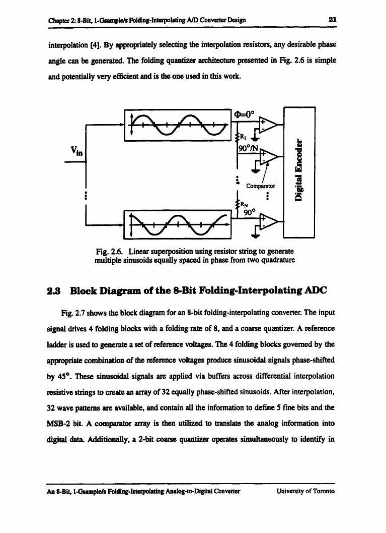
.................... zero-crossings ......................................... Fig . 2.6. Linear superposition using resistor string to generate multiple sinusoids equally
spaced in phase fiom two quachtute sinusoids ............................................................... 21
Fig.2.7. Block diagram of the 8-bit folding-interpolating ADC ..................................... 22
Fig . 2.8. (a) Folding circuit based on wireâ-OR interconncction (b) output waveform of the
folding circuit .................................................................................................................... 24
Fig . 2.9. Linear intefpolaîion between the outputs h m 2 folding blocks ..................... 25
......................... Fig . 2.10. Improved folding circuit using emitter degeneration mistors 25
................... Fig . 2.1 1 . Interpolation emr rcduced using eminer degeneration resistor ...2 6
Fig . 2.12. SimuIatioa outputs fmm 4 fo1ding bIocLs ....................................................... 27
Fig . 2.13. Block diagram of the folding interpolating blocks ................................et......... 28
Fig . 2.14. Simulation outputs h m dinerential mterpolations ......................................... 29

................... Fig . 2.15. Deviation of reference voltages caused by input bias cumnt b ..3û
Fig . 2.16. 2-stage preamplifier comparator circuit ................... ................................. .. 31
.................................... Fig . 2.17. 2-stage pnamplifier mastet-slave comparafor &cuit 32
Fig . 2.18. Input signals (top). clock signal (2nd). simulation output h m the master ................... comparator (thid). simulation output from the slave comparator (bottom) -32
Fig . 2.19. Block diagram of the 5-bit encoder ................................................................. 33
Fig . 2.20. EXOR circuit .................................................................................................... 35
Fig . 2.2 1 . Simulation output wavefonn h m the EXOR gate . Two inputs (Top) . EXOR
................................................................................................................ Output (Bottom) 35
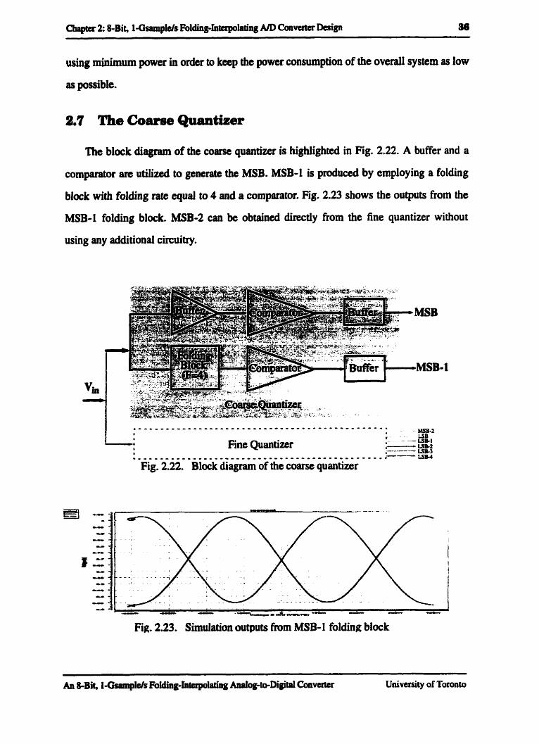
Fig . 2.22. Block diagram of the coarse quantizer .......................... .................. ............ 36
Fig . 2.23. Simulation outputs h m MSB-1 folding blodc ...........................*.................. .36
.................................. Fig . 2.24. Misalignment between a coarse ADC and a fine ADC 37
................... Fig . 2.25. Dynamic performance of the ADC simulation setup .............. 38
................... Fig . 2.26. Simulation dynamic performance of the ADC. input at Ml scale 39
Fig . 3.1. Cornparison of a tree-structure winng with a conventional wiring for a crucial
hi@-speed signal ............................................................................................................. -45
Fig.3.2. Layoutofthe ADCusingtheNTZS technology ...........................Cc.............. -47
Fig . 3.3. Micropp h of the implemented A/D converter ............................................... 48
Fige 3.4. Measund 8-bit output waveforms from the ADC for a low frequency ramp signai
50
................... Fig . 3.5. Measund dynamic performance of the ADC. input at full =aie 5 1
Fig . 3.6. A histognun for the figure of merit F on pnviously reported ADCs and the one
ceported hem ..................................................................................................................... -52
Fig . A.1. (a) FFI' of a pure sine wave with an ided converter. (b) FIT of a pure sine wave
................................................................................................... with a nonideal convertet 57
Fig . A.2. AID converter test setup ................................................................................... -58
List of Tables
Page
......................... Table 1.1 : Reported folding-interpolating monolithic Gsamplels ADCs 10
...................................................... Table 1.2. Target specincations of the A D conve* 12
Table 2.1. The reference voltage values of folding blocks ..............e............................... 27
Table 2.2. Themorneter and circular code npnsentation of the numbers 0-7 ................ 34
Table 2.3: The ADC Cbatacteristics .............~............................~..~...e...............................40
........................................................................... Table 3.1. Meâswed ADC pufonnmce 51
Cbapter 1: introduction 1
CHAPTER 1
Introduction
Analog-to-digital (AD) conversion and digital-to-analog (DIA) conversion lie at the
heart of modem signal pmessing systems when digital circuitry performs the bulk of the
complex signal manipulation. As digital signal processing (DSP) integrated circuits becorne
increasingly sophisticated and attain higher operating speeds, mon and more processing
hinctions an perfomed in the digital domain. Dnven by the enhanced capabüity of DSP
circuits, A/D converters (ADCs) must operate at ever-increasing fnquencies while
maintaining accuracy pmiously obtainable only at moderate speeds.
Digital systems offer significant advantages in k m of hinctionality, flexiiility, and
immunity against extemal influences compand to their analog counterparts, and as such are
becoming pervasive in electronic systems. Fig. 1.1 iliustrates the evolution of
communications systems towards relying upon DSP hardware with a concomitant reduction
m anaiog circuit content. This shift iadicates that ody Radio Fnquency (RF) prooessing
and data conversion (including anti-aüasing filters) will remain as important niches where
anaiog implementations exhibit advantages over digital approaches. Intedate
Fmpency (IF) and RF daîa conversion wiU continue to play a significant mie m advanced
communications systems. However. the charactcristics of ADCs fn<iuently liait the

Cbptcr 1: Introduction B
performance of such systems because of the circuit complexity and large power
consumption of high-speed A/D converters. The developmnt of improved A/D conversion
algorithmg and circuiûy CO meet the need of commW1ications systems represents an
important ana of research for the foteseeab1e future.
w Signal
Fig. 1.1. Examples of increasing DSP complexity in communication systems. (a) A classic system with analog demoduiator foiiowed by baseband A D conversion and DSP. (b) An advanced system with IF A/D conversion using digital demodulation and sipal processing. (c) An emetging system with RF A/D conversion foiiowed by digital domronversion, demodulation, and basedband signal pmcessing.
A variety of efforts have been made to increase the sampling speed of ADCs over past
years, but the evolution of wideband communications systems which take the advantage of
the Industrial, Scientinc, Medical (ISM) unlicensed frequency bands, especiaily in the 2.4
GHk band, and possiily in îhe 5.ûGHz baud [Il, are driviag the deman& for ADCs with
muiti-GsampIds capabilities. Howevtr, most ADCs with Gsamplds qeed are designed
using expensive GaAs-baseà and ïnP-based hcterojonction bipolar (HBT) processes [2,3,
An 8-Bit, l-OsamplJJ FoIdiag-hterpoiating Aaatog-to-Digital. Coilvmter University of Toronto
41, another drawback of IiI-V HBT processes is the pmblematic cornpatibility with DSP
systcms reaiizeà using silicon CM06 and BiCMOS processes. Further inmase in system
intepration requires that high-speed ADCs be impkmented using conventional silicon
proasses. This thesis is aimed at developing an 8-bit, Osamplels ADC using a silicon
bipolar pmcess.
1.1 A/D Converter Characteriotics and Architectures
1.1.1 A/D Converter Characterietics
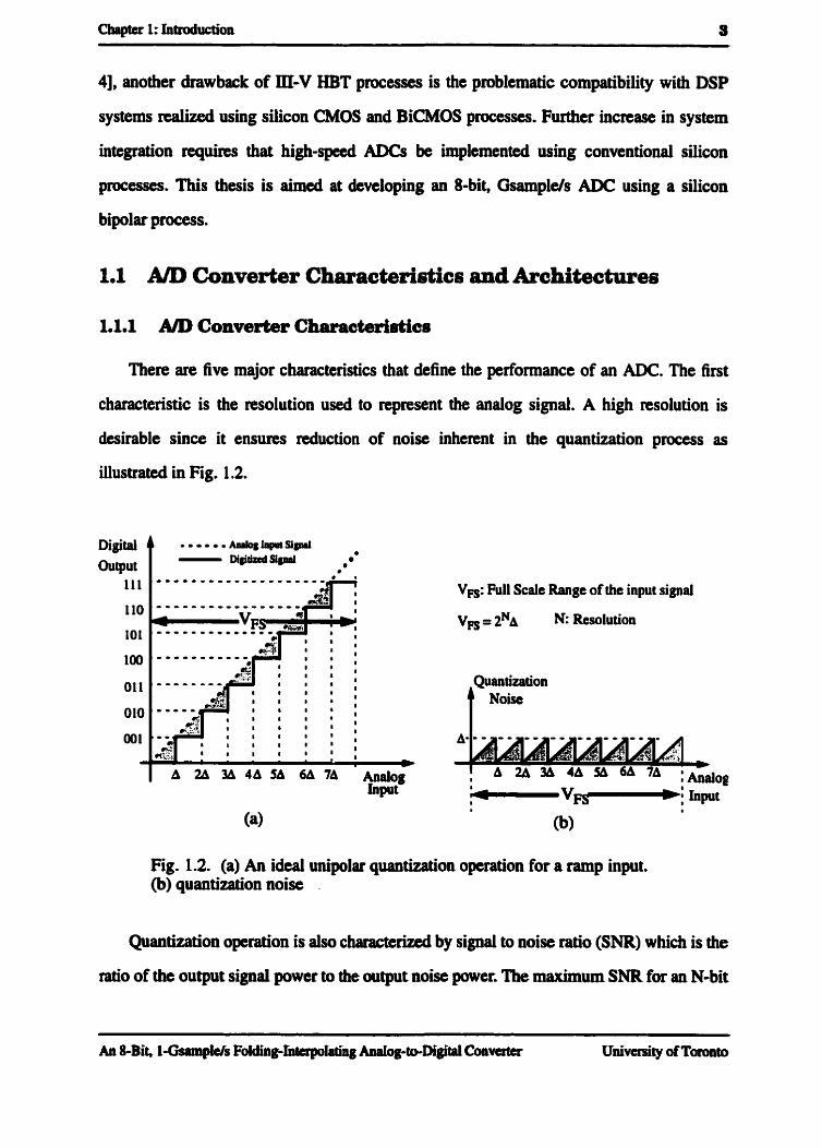
The= are five major characteristics that define the performance of an ADC. The first
characteristic is the nsolution used to represent the analog signal. A high resolution is
desirable since it ensures reduction of noise inheicnt in the quantization pmcess as
illustrateci in Fig. 1.2.
VFS: Full Scale Range of the input signal
v, = NA bk Ruolution
Quantization
t Noise
Fig. 1.2. (a) An ideal unipolar quantkation operation for a ramp input. @) quantization noise .
Quantization opemîion is also characterized by signal to noise ratio (Sm) whicb is the
ratio of the output signai power to the output mise power. The maximum SNR for an N-bit

Cbapter 1: Introduction 4
ideal converter with a sinusoidai input of amplitude equd to VpSn can be expressed as
foUows pl:
S s = 6.û2N + 1.76 (dB) (1-1)
For example, for a 10-bit converter the cmchum SNR is 61.97dB. However, in practice,
the SNR of most 10-bit A D converters is not able to reach this number. Using the actual
S N R and solving for the equivaient resolution, a figure of ment cailed the number-of-
effective-bits, Ncn, can be expressed as:
Tbnumkr-of-effective-bits, sometimes refemd to as effective-numôersf-bits (ENOB) is
a commonly used meEnc for characterizhg the performance of non-ideal quantizers. ENOB
or SNR (corresponding to a given ENOB) is the second important characteristic of an ND
converter.
The third characteristic of an ADC is the sampling rate. The sampling rate is the speed
at which analog input simples cm be continuously converted into a digital word. In most
applications the sampiing rate of an ADC is determined by the analog signal bandwidth,
because the sampling rate has to be at least twice the highest input frcquency in accordance
with Nyquist's theorem. Power dissipation is the fourth characteristic of an ADC. 'Spically,
high-cesolution and high-spad ADCs tend to consume more power than simpler low-
cesolution designs. FiaUy, the last characteristic is the chip area which, in gened, should
be minimum.
A variety of architectures exist for implementing ADCs. Tbey ye classifieci as pamIlel,
fee-ck and fee#orwurd convcrters [6J. Each z~~c:hitectare offers specific advantages.

Chaptcr 1: Introduction 6
Parailei converters such as Bash converters are usudy used for very high-speed daîa
conversion. Fige 1.3 presents the architcctwe of such a converter. In this architecture, an
array of comparators simdtaneousIy compares the input voltage with a set of referenœ
voltages. The outputs of the comparators represent the input signal in a set of thennometer
codes that can be eady convertai into a binary code. Flash converters are inherentîy fat
due to their padelism. However, this architecture has a significant drawba~k when a high
resolution conversion is &si&: namly, the number of comparators grows exponentially
with the molution. In addition. the sepmtion of adjacent nference voltages grows smaiier
exponentially with the resolution bit. This nsults in: difficulties in matching components, a
very large chip area, a high power dissipation and a large input capocitance that nduces
analog input bandwidth. For example, an 8-bit lash ADC with 250 Msamplels smpling
rate occupies an acea of 3 1 m 2 and dissipates 12W of power [A. Most lash converters
available today have less than 8-bit resolution.
Analog Input
Fig. 1.3. A block diagram of flash converter
Digitai - Output

Cbspter 1: Introduction 6
Feedback converter architectures d u c e complexity compand with the p d e l
approach by utiiizing comparators multiple times during each quantization 18-121. In this
architecture as shown in Fig. 1.4, the NL N-bit dipitizing process is divided into a series of
low resolution. m-bit quantizations. Each of these steps begins by ampiifying the Uicomiag
signal apptopriately, foflowed by a coarse m-bit quantkation. The digitai result from this
operation is appîied to a special accumulator callecl a Successive Approximation Repister
(SAR), the output of which drives an N-bit DIA converter. The analog output Rom the DAC
subtracts fiom the input signal to fom a residue signal which is ready for the next pass
through the feedback loop. The N-bit resolution obtained with this arrangement is govemed
by N=mp where m is the resolution of the coarse quantizer used, and p is the number of
passes amund the lwp required to produce each N-bit output code. The gain of the
amplifier preced'ig the m-bit quantizer must be increaseà at each successive pass amund
the feedback lwp to ensure that the coarse quantizer is driven with the proper amplitude.
The gain required to meet this condition is:
Gain Stage
Input Residue > L
Successive Approximation Register
N-bit Digitai Output
Eg. 1.4. A block diagram of feedback converter
m 4=2"'~i)
Controllable
m-bit Quantizer
Feedback A/D converters can offer signifcant hardware savings compared to paralie1
converters because the coarse quantizer resolution m cm be much smaller than the
converter resolution N. The severe dmwback of the feedback architecture is that it requins
p=N/m passes to generate the full N-bit output word, limiting maximum throughput rate,
and thenfore ümiting the speed of conversion. The feedback architecture is an excellent
candidate for very high-resolution, Low-speed convenions.
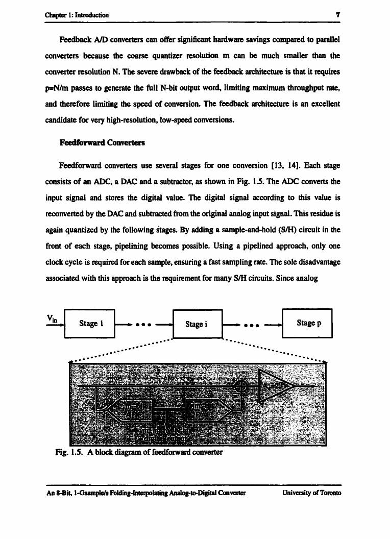
Feedforward converters use several stages for one conversion [13, 141. Eacb stage
consists of an ADC, a DAC and a subtractor, as show in Fig. 1.5. The ADC converts the
input signal and stores the digital value. The digital signal according to this value is
reconvened by the DAC and subtracted from the original analog input signal. This nsidue is
again quantized by the following stages. By adding a sample-and-hold (SRI ) circuit in the
front of each stage. pipelinhg becornes possible. Using a pipelined approach, only one
dock cycle is required for each sarnple, ensuring a fast sarnpüng rate. The sole disadvantage
associateci with this approach is the requinment for many S/H circuits. Since analog
switches (fiiaâamental to S/H operation) are difficuit to impkment using bipolar
components, most pipehed A/D converters utiüze CMOS processes [1E18].
Each of the three converter architectures mentioned Pbwt offers a pedormance trade-
off. A designer must choose the appropriate architecture based upm the target
specincations and applications. In general, parallel converters are used when low resolution
(less than 8-bit) and very high speed is nquind. Feedback converters are chosen when low
speed but very high nsolution is cequind. Feedforwud converters are suitable for high
speed and high resolution applications.
To be used in wideband cornmunications systems, N D converters must meet very
stcingent requirements. If the input signal is sssumed to lie within the IF/RF band in suc&
applications, sampüng rates in the cange of 200-Msamplels to multi-Gsample/s are q u i n d
to satisfy Nyquist's criterion. In addition, a 6 to IO-bit resolution is generally requid [2,
19, 201. However, the resolution and the sampling rate are nlated. State of the art N D
converters show that the pmduct of the nsolution and the sampling rate is roughîy a
constant for a particular process. The nsolution falls off by about 1 bit for every doubling of
the sampling rate (21,221.
The previously mentioned A/D converter architectures are not able to meet the
nquirements for Gsamplds speed and 8-bit resdution simultaneously. Fominately, a
folding architecture can overcome the drawbacks of p d l e l converters while ntaining the
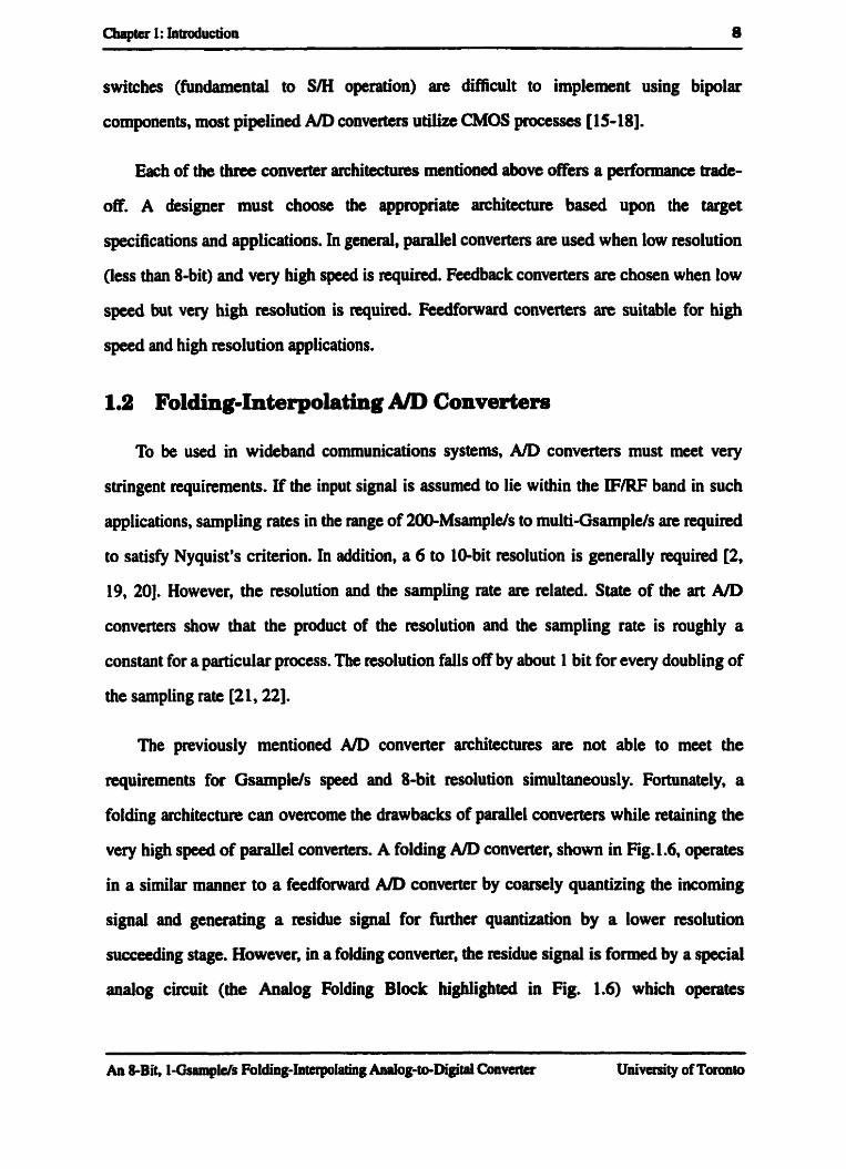
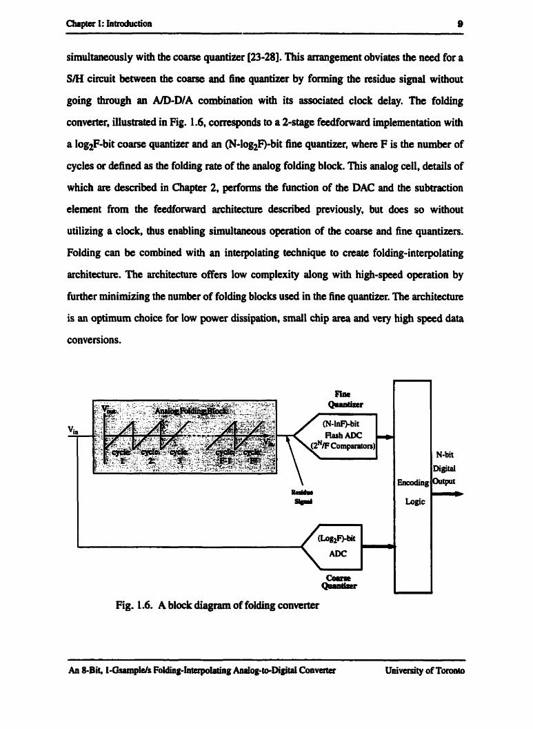
very high spaod of p d e l converm. A folding AID converter, shown in Fig. 1.6, operates
in a similar rnanner to a fdorward A/D converter by coarsely quantizing the incoming
signai and generating a &due signai for fiuthcr quanthtion by a lower resolution
succeeding stage. However, in a folding converter, the &due signal is formed by a specïal
analog circuit (the Analog Folding BIock higblighted in Fig. 1.6) which operates
An &Bit, 1-GsampWs Folding-IntepIating Anaiog-to-Digiial Converter University of Toronto
Chapter 1: Introduction 8
simuitaneously with the CO- qyantizer [23-281. This arrangement obviates the n a d for a
SM circuit between the coarse and fine quantizer by forming the cesidue signal without
going thmugh an A/D-DIA combination with its associateci clock May. The foldirg
converter, iliustrated in Fig. 1.6, corneponds to a 2-stage fadfomard Unplementation with
a log#-bit coarse quantizer and an (N-log2F)-bit fine quantizer, when F is the number of
cycles or defined as the folding rate of the analog folding block. Tbis analog cell, details of
which are described in Chaptet 2, perforrns the hinction of the DAC and the subtraction
element from the feedforward architecture described pmriously, but does so without
utilizing a clock, thus enabling simultaneous operation of the coarse and fine quantizers.
Folding cm be combined with an interpolating technique to create folding-interpolating
architecture. The architecture offers low complexity dong with high-speed operation by
further minimizing the number of folding blocks usai in the fine qumtizer. The architecture
is an optimum choice for low power dissipation, small chip area and very high s p d data
conversions.
Fig. 1.6. A block diagrmi of foldmg converter
An %Bit, I-Gsarnplels Foldiag-Interpotating AnaI~~to-Digitai Converter University of Toronto
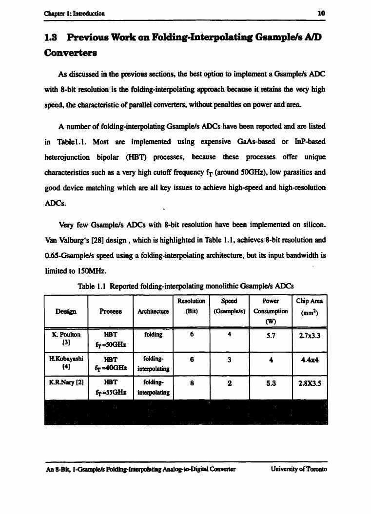
1.3 Previous Work on Folding-Interpolating GsampIe/s AID
As discussed in the previous sections, the best option to implement a GsampWs A I X
with &bit nsolution i s the foldiog-inteplathg approach because it retahs the very high
speeà, the characteristic of patallel converters, without penalties on power and area
A number of folding-interpolating Gsamplds ADCs have been reported and are listed
in Table 1.1. Most are implemented using expensive GaAs-based or InP-based
heterojunction bipolar (HBT) processes, because these processes offer unique
characteristics such as a very high cutoff frequency fT (around SOGHz), low panisitics and
good device matching which are al1 key issues to achieve hi&-speed and high-nsolution
ADCs*
Very few Gsamplds ADCs with Cbit resolution have been implemented on silicon.
Vàn Valburg's [28] design , which is highlighted in Table 1.1, achieves &bit resolution and
0.654samplds speed using a folding-interpolating architecture, but its input bandwidth is
liaiited to ISOMHz.
Table 1.1 Reported folding-interpolating monolithic Gsarnplels ADCs
K. Poulton HBT 6 4 5.7 2.7~3 .3

Themm Objective and Outline
The main objective of this thesis is to ûevelop an 8-bit, LGspmplels ADC with
minimum power dissipation and minimum chip area using the NT25 silicon process. The
N D converter with 8-bit, I-OsamplJs speed has applications in d b c t IF sampiing
nceivers for wiâeband cornrnunications syskrns. Direct sampling cecenters offer significant
advmtages over conventional nceivers by digitking the analog signal at a point closer to
the anteano. The receivers offer such advantages as reduced size, weight and power and
iacnased flexibility. huictionality and noise imrnunity [2].
The NT25 process used for this project is provided by Norte1 Networks. The process is
o 0.5 pm self-aligned. double poly silicon bipolar process with maximum unity gain cutoff
fiequency fT of =GHz*. This proccss provides NPN transistors. difised and polysilicon
resistors, and triple layer metal interconnection [29].
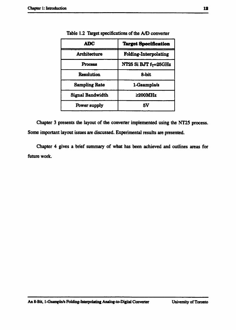
The target specifications of the converter are listed in Table 1.2. A folding-interpolating
architecture was chosen to achieve the desircd spcifications. Input signal bandwidth was
chosen to be greater than 200MHz which covers most of IF fquency band in wideband
communications systems.
The thesis is organized as foilows. Chapter 2 describes the architecture of the folding-
interpolating ADC. It investigates the design of the major building blocks necessary to
implement the ADC. Simulation results are pcesented.
* Tba unity gain fkqucncy fT is 2508t for a minimum emiücr size dcvice ( 0.SXl3p~) .
1 Sampling Rate 1 l-Gsamplele
Table 1.2 Target specifications of the A/D converter
Chapter 3 presents the layout of the converter implunented using the NT25 process.
ADC
Architechve
Some important layout issues are discussed. Experimental results are presented.
'kget ûpecifluation
Folding-hterpolating
Chapter 4 gives a brief summary of what has ken achieved and outlines mas for
future work.
Chapter 1: Introduction 18
Refeiences [il C. Bisdikian, Bhagwat, B. P. Gaucher, F. J. Jamielio, M. Naghshineh, P. Pandoh and
1. Kofpeoglu, 'WISAP: A Wmicss Personai Access Network for Hanâheld Computing
Devices," IEEE personal Communications, vol. 5, n0.3, pp. 18-2!5,1998.
[2] K. R Nary, R. Nubling, S. Beccue, W. T. Collean, J. P e ~ e y and K. C. Wang, "An 8-
Bit 2 Gigasample per Second Analog-to-Digital Convertef' ZEEE GoAs IC Sympo-
sium, ïèchnical Digest, pp. 303-306, 1995.
[3] K. Poulton, K. L. Knudsen, J. J. Corcoran, KC. Wang, R. B. Nubüng, R L. Pierson, M.
F. Chang, P. M. A s k k and R.T. Huang, "A dbit, 4GSals ADC Fabricated in a GaAs
HBT Pmcess," IEEE G d s IC Symposium, Techical Digest, pp. 240-243, 1994.
[4] H. Kobayashi, T. Tobari, H. Matsuura, A. Miura, Mo Yamanaka, T. Yakihara, S. Koba-
yashi, S. Oka, T. Fujita and D. Murata, "System Architecture and Key Components of
Multi-Giga-Hertz A D Converter with HBT," IEEE I~tstrumentation mid Measurements
Technology Conference, Pmceedings, pp. 1 160- 1 166, 1996.
[SI Do A. Johns and K. W. Martin, Analog lntegrtzted Circuit Design, John Wiky & Sons,
Inc., Toronto, Canada, 1997.
[6] J. Sauerer, R. Hagelauer, F. Oehler, G. Rohmer, U. schlag, D. Seitzer, T. Grave, W. kell-
ner, ''System Architecture and Key Components for An 8 Bitll GHz OaAs MESFET
ADC," lEEE G d s IC Symposium, ïèchnical Digest, pp. 105-108,1992.
[7] B. Peetz, B. Hamilton and J. Kang, "An &bit 250 Megasample per Second Anaiog-to-
Digital Converter: Operation Without a Sample and Hold,YIEEE Jountat of SolMtate
Ckuits, vol. 21, pp. 997- 102.1986.
[8] M. Koliuri, "A Muiti-Step Paraîle1 lob l . S p ADC," IEEE Intemational Soli&State
Cimits Cot&emnce, Digest of Technical Papem, pp. 60-6 1,1984.
Chapter 1: Introduction 14
[9] J. Fernandes, S. R Lewis, A. M, MaMnson, and G. A Miller, 'X lebit lOms Sub
Ranging A D Convertet with Sm," IEEE Intemtiomd Solid-Stute C i m u i ~ Confier-
ence, Digest of Technical Papen, pp. 230-23 1,1988.
[IO] B. S. Song, S. H. Lee, and M. F. Tompsett, "A IO-b 15MIIz CMOS Recycüng 'Itvo-
Step A/D Converter: IEEE Joumal of SolidStute Cimuits, vol. SC-25, pp. 1328-1338,
1990.
1111 R. J. Van De Plassche and H. J. Schouwenaars, "A MonoIithic lebit AD Converter,"
IEEE Juuml of Solid-Staîe Circuits, vol. 17, pp. 1 1 1 2- 1 1 17, 1982.
[12] H. S. Lee, D. A. Hodges and P. R. Gray, 'A SeKCalibrating 15-bit CMOS A/D Con-
verter:' IEEE Joumal of Solid-state Ci~uits. vol. 19, pp. 81 30819,1984.
[13] M. Yotsuyanagi, T. Etoh and K. Hirata, "A 10-b SOMHz Pipelined CMOS A/D Con-
verter with SM," IEEE humal of Solid-State Circuits, vol. 28, pp. 292-300, 1993.
1141 W. T. Colleran and A. A. Abidi. "A IO-b, 75MHz Two-Stage Pipelined Bipolar AD
Converter," lEEE Jouml of Solid-State Circuits, vol. 28, pp. 1 187-1 199, 1993.
[15] N. Fuhishima, T. Yamada, N. Kumazawa, Y. Hasegawa, and M. Soneda, "A CMOS
4ûMHz, 8b 10SmW liwo-Step ADC:' IEEE Intemational Soltd-State Circuits Confer-
ence, Digest of Technical Paprs, pp. 14-1 5,1989.
1161 S. H. Lewis and P. R. Gray, "A Pipelincd SMHz 9b ADC," IEEE Intenarionul Solid-
State Cimuits Confernice, Digest of Technical Papers, pp. 2 10-2 1 1,1987.
[lq Y. M. Lin, B. Kim, and P.R.Gray, "A 13-bit. 2.SMLlz Self-Caiibrated Pipelined A/D
Converter in 3-pm CMOS." IEEE Journul of Solid-State CirnUs, vol. SC-26, pp. 628-
636,1991.
[18] B. S. Song and M. F* Tompsett, "A 12-bit lMHk, Capacitor Error Average Pipelined
A/D Converter," IEEE Intetnatio~l SolUI-State Cimuits Confemce, Digest of ïèchi-
cal p ers, pp. 226427,1988-

[19]M. J?iynn, B. Sheahan, "A 400-Msamplels, 6-b CMOS Folding and InterpoIating
AMI: ZEEE Joumal of Solid-State Circuitts, vol. 33, pp. 1932-193 8, 1998.
[20] D. Falconet and G. Stamatelos, "LMDS System Architecture and Associated Research
Issues," CITR B t v a à h à WinlcJs Major Pmject, Carleton University, Ottawa,
Ontario, Canada.
[21] Je Sauerer, F. Oehler, G. Rohmer, U. Schlag, "GaAs for ADCs: System Needs and
Device Requirements," IEEE GaAs IC Symposium, Techical Digest, pp. 220-223,
1994,
[22] R. H. Walden "Analog-to-Digital Converter Tecbnology Cornparison:' IEEE GaAs IC
Symposium, ïkchnicat Digest, pp. 21 7-2 19,1994. m
[23] A. Arbel and K. Km, ''Fast ADC," IEEE T m Nucl. Sci., vol. NS-22, pp. 446-45 1,
1975.
[24] R. van de Grift and R. J. van de Plassche, "A Monolithic 8-bit Video A D Converter,"
IEEE Journal of Sotid-Stute Circuits, vol. SC-19, pp. 374-378, 1984.
[25l U. Fiedkr and D. Seitzer, "A HighSpeed %bit An> Converter Based on Multiple Fold-
ing Circuit: I E E JouwI of Solid-Sate Cimuits, vol. SC-14, pp. 547-551, 1979.
[26] R. van de Grift and M. van der Van, "An 8b S O M H z Video ADC with Folcüng and
Interpolation Techniques," IEEE Intemutional Solid-State Cincuits Conference, Digest
of Technicd Papen, pp. 9445,1987.
1271 R J. van de Plassche and P. Baltus, "An 8-bit lûûMHz Full-Nyquist Analog-to-Digital
Converter," lEEE Journal of SolU1-State Circuits, vol. 23, pp. 13341344, 1988.
[28] J. van VaIburg and R. J. van & Plassche, "An 8-b 65GMtlz Folding ADC," IEEE Jorcr-
na1 of SolidState Cimuits, vol. 27, pp. 1662-1666,1992.
[29]NnS HectnCai Specificatiotls ond krywt Design Rtdes, kmbn IS01.2 CMC, June
27,1997.
CaAPTER 2
&Bit, 1-Gsampleh Folding-Interpolahg A / ' Converter Design
2.1 Introduction
As described in Chapter 1, (2N-l) comparators are nquired to compare the analog input
voltage with (2N-l) thresholds for an N-bit conversion in a conventional flash ADC. The
number of comparators becornes unacceptable when the required molution is greater than
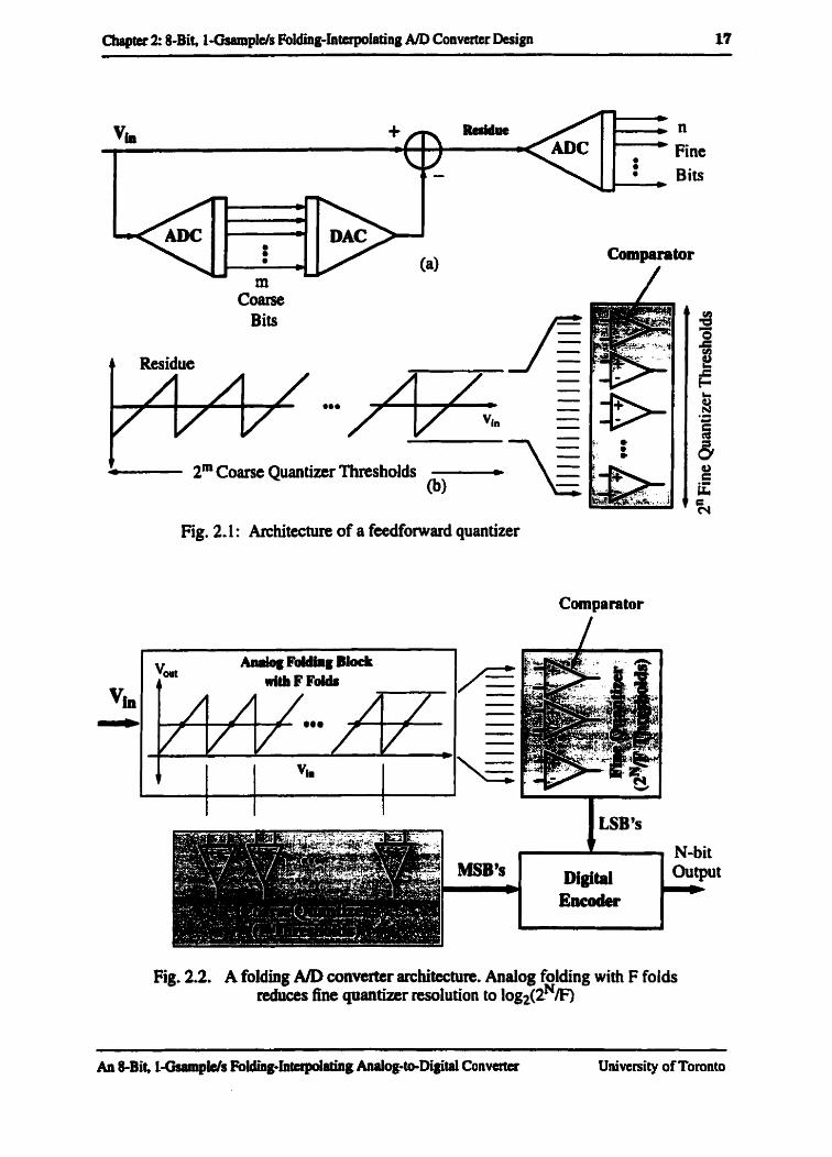
6. This problem can be ovcrcome by employing a feedforward multiatage A/D converter
which partitions the N-bit quantization into a number of lower-resoluiion quantizations. In
such a converter, shown in Fig. 2.la, an m-bit coarse quantizer digitizes the input signal
with low nsolution, and applies the nsultant code to a reconstruction DAC. The anaiog
output of the DAC is then suùtracted from the original input to form a nsidue signal, as
shown in Fig. 2.lb. This residue is quantized by an n-bit fine quantizer. The advantage of
this appmach is due to the fact that the combined complexity of the m-bit corne quantizer
and the n-bit fine quantizer can be far less than the complexity of a single (rn+n)-bit
qumtizer. In a foldmg quantizer, s h o w in Fig. 2.2, the nsidue signal is formed with a
simple anaiog circuit, thenby obviating the need for the coarse quantizer, the DAC, and the
subtracter components as in Fig. 2.la In such an implementation, the low dynamîc-range
midue signal geaerated by the d o g folding circuit ditectly drives the fine quantizer.
An %Bit, î-GsPmpI J s FoIding-IntqoIating Aaaiog-to-Digital Converter University of Toronto
Chaptw 2: 8-Bit, L-Gsamplds Folding-interpolating A/D Converter Design 17
* +p, Rcddm , n
Fine a : Bits
m Coarse
Bits
t - 2' Coarse Quantizer Thresholds - (b)
Fig. 2.1 : Architecture of a feedfoward quantizer
Comparator
Fig. 2.2. A foldhg A/D converter arcbitechm. Anaiog folding with F foi& ceduces fine quantizer resolution to log2(2NIF)
-
An &Bit, I-OsampWs Folding-IntapoIating Analog-bDi8ital Converter University of Toronto

Bccausc of the periodic na- of the residue signal, the digitized output h m the fine
qumtizer is ambiguoust aiid a caarse converter is still necessary to ascertaign in which p e n d
the qoantizer input signal lies. The input-output characteris tics of the analog Foldi ng circuit.
illustratecl in Fig. 2.3, cm be parametecized by the numkr of piece-wise linear segments. or
folds; the number of fol& or folding rate, denoted as Ft detefinines the resolution of both
the CO- and fine quantizers cequked in a folding AD converter. Since the coarse
quantber quires F thnsholh, its nsolution is m=log2F whiie the fine quantizer requins
2 N / ~ thrrsbolds so that its resolution is n=10~~(2~/F), The number of comparators required
is therefore nduced by a factor of ' The main disadvantage of folding is the multiple
fnquency effcct inherent in the process.
b
0 1
Folding ; Convcrtcr :
I
- - Fold Fold Fold Fold
1 2 F-1 F AiD input Signal
(b) Fig. 2.3. Muction in dpdc range seen h m comparator anay
(a) sawtooth folding ~hatactcristic~ (b) triangle folding characteristic
An &Bit, lGampWs Folding-Inaipolating AnJog-to-Digital Converter University of Toronto
Cbapec 2: 8-Bit, l-OsampIJs Folding-ïnierpolatiag A/D Convuter Design 19
BS Folding and Interpolation 'bchniquee
A folding A/D converter, based on the architecture of Fig. 2.2, would be possible if a
simple malog circuit could easily d i z e the picce-wise ünear input-output characteristics
indicatcd in Fig. 2.3. However, because of the discontinuity in the folding transfer function.
these types of characteristics are inhenntly difncult to nalize. Several implementations
baseâ on Uie translinear prtncipk have k n &vcloped to approximate the triangle wave
folding characteristic of Fig. 2.3, but few are used in practice due to the significant
dtawbacks associated with the very large input swing nquind for these implementations
[L-31. This voltage swong is unacceptably large for the low-power, high-frequency
application considend hem.
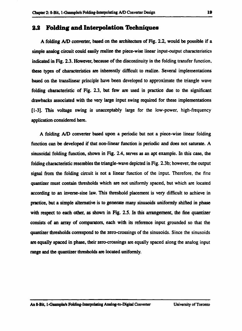
A folding A D converter based upon a pModic but not a piece-wise lintar folding
function can be developed if that non-Iinear function is periodic and does not saturate. A
sinusoiciai folding ninction. shown in Fig. 2.4, sems as an apt example. In this case, the
folding characteristic resembles the triangle-wave depicted in Fig. 2.3b; however. the output
signal h m the folding circuit is not a linear function of the input. Therefore, the fine
quantizer must contain thresholds which are not unifonnly spaced but which an located
according to an inverse-sine Iaw. This thnshold placement is very difficult to achieve in
practice, but a simple aiternative is to generate many sinusoids uniformiy shifted in phase
with respect to each other, as shown in Fig. 25. In this arrangement, the fine quantizer
consists of an array of comparators, each with its reference input grounded so that the
quantizer thrrsholds comspond to the zero-crossings of the sinusoids . Si nce the sinusoids
are quaiiy spaced in phase, their zero-crossings are equally spaced along the analog input
range and the quantizef tlnuholds are Iocated uniformly.
An &Bit, 1-Ws F~ldin~fnterpoIating Analog-to-Digital Converter Univtmmty of Toronto

Fig. 2.4. A folding function which is not piece-wise linear
Corn pantuf a
Fig. 25. An anay of phase-shifted, non-linear folding blocks with comparators detecting zero-crossings
Generating the phase-shiftcd wavefoms with an m y of sinusoidal folding circuits
wouid be very iwfsciant. but a simpIification of the scheme depicted in Fig. 2.5 obviates
the neeâ for this type of ndundaacy. Instead, only two sinusoids are geoerated. illustrated in
Fig. 2.6, and the ccmaining sipals arc obtained by linear superposition between them. Om
tcchniqyt, iliusaated in Fig. 2.6. for achieving the superposition utilizes resistive
An &Bit, I-OsampIJs FoIdïng-htetpolating Mog-&Digital Coavertcr University of Toronto
Cbapter 2: %Bit, l-Gsamp1 Js Folding-hterpobkg AID C o n v ~ r r Design 31
interpolation (41. By appropriately stlecting the interpolation nsistors, any desirable phase
angle cm be generated. The foldhg quautizer architecture presented in Fig. 2.6 is simple
and potentiaüy very efficient and is the one used in this w o k
Fig. 2.6. Linear superposition using resistor string to generate multiple sinusoids equally spaced in phase fiom two quaciratme
2 1 Block Diagram of the &Bit Folding-Interpolating ADC
Fig. 2.7 shows the block diagram for an &bit folding-interpolating converter. The input
signai drives 4 folding blocks with a folding rate of 8, and a coarse quantizer. A reference
ladder is used to generate a set of reference voltages. The 4 folding bl& govemed by the
appropriate combination of the nfennce voltages produce sinusoidd signds phase-shifted
by 45'. These sinusoiclai signals are applied via buffers across differentiai interpolation
resistive strings to mate an array of 32 equdy phase-shifted sinusoids. After interpolation,
32 wave patterns are availabk, and contain al1 the information to define 5 fine bits and the
MSB-2 bit. A compamtot array is then utilized to translate the analog information into
digîtai datk Additionally, a 2-bit coarse qaantizer operates simultaneously to identify in
--
An &Bit, L-GsrimplJar Folding-Interpofaiing Analog-to-Di&itai ConvertCr University of Toronto

Chapter 2: 8-Bit, 1-GsmipWs Foldiog-Interpolating A/D Coavcrter Design a2
which cycle of the folding characteristic the input signal lies. Finaily, a digital encoder is
nquind to obtain the 8 binary digital codes.
The design of each building block will be investigated individually in the following
sections. The simulated performance will also be presented.
4 X 8 K 8 =256 8 Fdding Folhg Times =2
Block Rate Inteipo(iiti011
Fig. 2.7. BIock diagram of the 8-bit foldiag-interpolating AM3
An &-Bit, l-Gsrmpfe/s Folding-Interpolariag Anaiog-@Digital Convertcc University O t Toronto
Chaptct 2= &Bit, I-Gsainpiels FoIdiaÏIiiterpolating AID Convertet Design 23
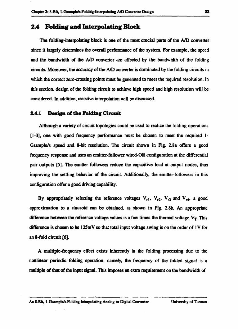
2.4 Folding and Interpolating Block
The folding-interpolating block is one of the most crucial parts of the AID converter
since it largdy detemines the ovcratl performance of the system. For example, the speed
and the bandwidth of the A D converter are affected by the bandwidth of the folding
circuits. Moreover. the accutacy of the A/D converter is dominated by the folding circuits in
which the correct wo-cmssing points must be generated to meet the requircd molution. In
this section, design of the folding circuit to achieve high spced and high resolution will be
consi&d. In addition, resistive interpolation will be discussed.
1.4.1 Design of the F01ding Circuit
Althougb a variety of circuit topologies could be used to realize the folding operations
[l-31, one with good fkquency performance must be chosen to rneet the required I -
Gsamplds spad and &bit resolution. The circuit shown in Fig. 2.8a offers a good
fkquency rwponse and uses an ernitter-follower wireâ-OR configuration at the differential
pair outputs [a. The emitter followers reduce the capacitive load at output nodes. thus
impmving the settiing behavior of the circuit Additionally, the edtter-followers in this
configuration offer a good dnving capability.
By appmpriately sekcting the refennce voltages VrI, V,, Vn and Vr4, a gOOd
approximation to a sinusoid can be obtained, as shown in Fig. 2.8b. An appropriate
diffecence between the refmnce voltage values is a few times the themai voltage VF This
ciifference is chosen to k l2SmV so that totaI input voltage swing is on the order of IV for
an 8-fold circuit [6].
A muitipIe-freciuency effect exists inherentiy in the folding processing due to the
nonhear periodic folding operation; namely, the fkquency of the folded signal is a
multiple of that of the input signal. This imposes an extra requirement on the bandwidth of
An &Bit, 1-GmnpIe/s Folding-interpolahg Analog-to-Digital Converter University of Toronto
Cbapter 2 8-Bit, I-Gssunplds Folâing-InterpoIating ND Converter Design a4
Fig. 2.8. (a) Folding circuit bared on wired-OR interconnection (b) output waveform of the folding circuit
folding circuits, especially for wideband applications. The circuit architecture and bias
conditions of the transistors in the circuit play an important role in detemiinhg the circuit
bandwidth. The option of bias conditions is a tracle-off between the bandwidth and power
consumption. In addition. the bandwidth of the circuit in Fig. 2.8a is inversely proportional
to the value of Rt. A large RL gives rise to a serious analog bandwidth limitation. However,
to nduce the sensitivity to offet in the rest of the converter, the value of the resistor Rt has
to be large enough to obtain a large output voltage.
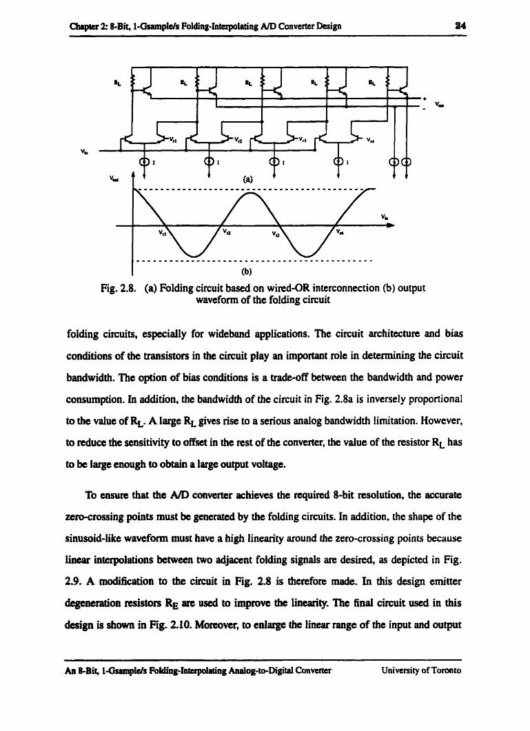
To ensure that the AID converter achieves the rcquired 8-bit resolution, the accurate
zetpcrossing points must be generaîed by the folding circuits. In addition, the shape of the
sinusoid-üke waveforrn must have a high linearity around the zero-crossing points because
hear interpolations between two adjacent foldiag signals are deskd. as depicted in Fig.
2.9. A modification to the circuit in Fig. 2.8 is therefore made. In this design emitter
degentration nsistm RE rilc uscd to improve the iinearity. The finai circuit used in this
design is shown in Fig. 2.10. Moroovu, to edacge the limm range of the input and output
Aa &Bit, L ~ f d s Folding-Intcrpolating Analog-to-Digital Converter University of Toronto
Cbaptcc 2: Mit, t-GsampW Folding-Intepolating îVD Converter Design 26
voltage swings, the c m n t source 1 inFig. 2.8 can be split into two equd cumnt soums T/2
tbat directly flow h m the two transistors in the di&nntiai pairs as show in Fig. 2.10.
Note that 8 refcrence voltages are nquind in Fig. 2.10 because a folding rate of 8 is used.
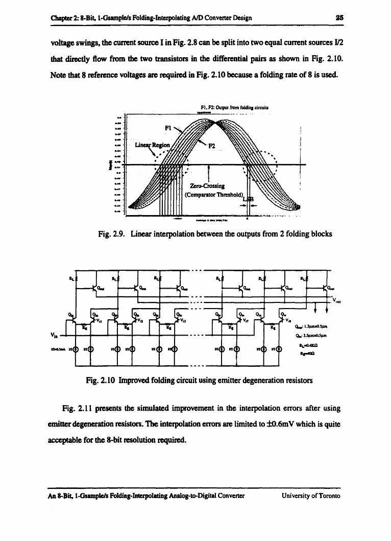
Fig . 2.9. Linear interpolation between the outputs fiorn 2 folding blocks
Fig. 2.10 Impmved fo1cüng circuit using emitter degeneration nsistors
Fig. 2.1 1 presents the sidated improvement in the interpolation errors after using
emitter degeneration mistors. The htcrpolation errors are limited to fO.6mV which is quite
acceptable for the &bit resoIution required.
An &Bit, 1-GsampWs Folding-Interptaîing Anaiog-ta-Digital Converter University of Toronto
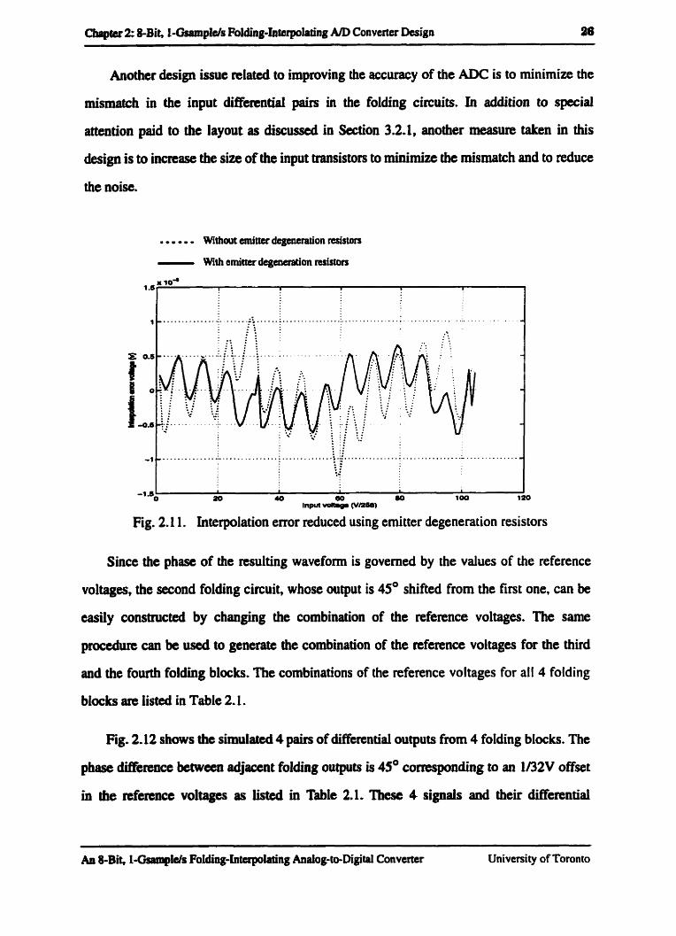
Another design issue related to improving the accuracy of the ADC is to rninimize the
mismatch in the input differentid pairs in the folding circuits. In addition to special
attention paid to the layout as discussed in Section 3.2.1, another measure taken in this
design is to increase the size of the input transistors to minimize the mismatch and to duce
the noise.
...... Without emitter degencration nsistots
- With cmittcr dcgendon mistors
Fig. 2.1 1. Interpolation emr reduced using emitter degeneration resistors
Since the phase of the nsulting wavefonn is govemed by the values of the reference
voltages, the second folding circuit, whose output is 45' shifted from the first one, cm be
easiiy constructed by changing the combination of the reference voltages. The same
procedure can be used to generatc the combination of the ceference voltages for the ihird
and the fourth foldhg blocks. The combinations of the reference voltages for al1 4 folding
blocks are Iisted in Taôle 2.1,
Fig. 2.12 shows the shulried 4 pairs of Werential outputs h m 4 folding blocks. The
phase Merence between adjacent folding outputs is 45' corres~onding to an 1/32V offset
in the referma voltages as iisted in Toble 2.1. These 4 signais and their differentiai
--
An 8-Bit, l-GsampI J s FoIding-Interpolating Analog-to-Digital Converter University of Toronto
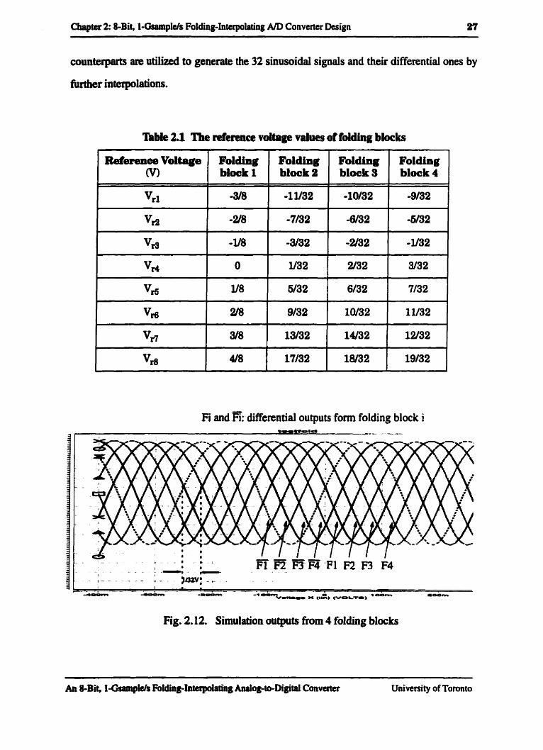
Cbaptcr 2 &Bit, 1 - ~ p I e / s Fo(diag-lntcrpolating A/D Converter Design 27
counterparts aie utilized to generate the 32 sinusoidd signals and their differential ones by
fkher interpolations.
nbie 2.1 The derence voltage valws of lolding blacks
I Reiemce Voltage Folding Fol- Folding Folding (V) 1 blaLl / blocka 1 bla*8 1 biockl
Fi and Fi: diffenntial outputs form folding block i
Fig. 2- 12. Simulation outputs h m 4 foldmg blocks

-ter 2 &-Bit, 1-Gsrmplds FoIding4nupolating A/D Converter Design a8
The interpolation is implemented using a nsistive string because of its simplicity and
powercfnciency 171. In tbis dasip. a more detailed diagram of Fig. 2.7 is redrawn in Fig.
2.13. Differential interpolations are implemented by applying the differential outputs of the
Fig. 2.13. Block diagram of the fdding intcrpolatiag blocks
-- pp -
An &Bit, I-Gs~l~lplds Foldùig-hterpolating Analog-to-Digitd Converter University of Toronto
Cbapter 2 8-Bit, 1-OsampklsF~Iding~Interpotating A D Converter Design 2B
foldiag blocks to the dinerential nsistive strings. The dinecentid implementation improves
the accwacy of the converter shce the coqaratoc operates on the di&rence between
sigaals and not on the absolute value of the signal.
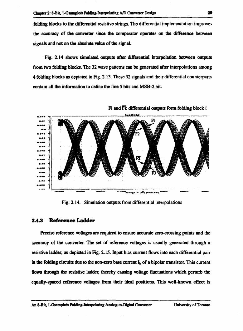
Fig. 2.14 shows shdated outputs after MercntiaI interpohtion berneen outputs
fiom two folding blocks. The 32 wave patterns can be generated after interpolations among
4 folding blocks as depicted in Fig. 2.13. These 32 signais and their differential counterparts
contain 8U the information to define the fine 5 bits and MSB-2 bit.
Fi and fri: dicerentid outputs fonn folding block i
Fig. 2.14. Simulation outputs fmm differential interpolations
h i s e reference voltages am requM to ensun accurate zefolcmssing points and the
accuracy of the converter. The set of reference voltages is usuaily pnerated through a
nsistive ladder, as depicted in Fig. 2.15. Input bias cumnt fiows into each difkrential pair
in the folding circuits due to the non-zero base cumnt 4 of a bipolar transistor. This cumnt
flows through the resistivc ladder, thenby cauaiag voltage fluctuations which perturb the
equaiiy-quxd rcftrtncc voltages h m th& ideai positions. This we11-known effkct is
An &Bit, t-GsampIe/s F~Idin~InterpoCating Analog-to-Digital Converter University of Toronto
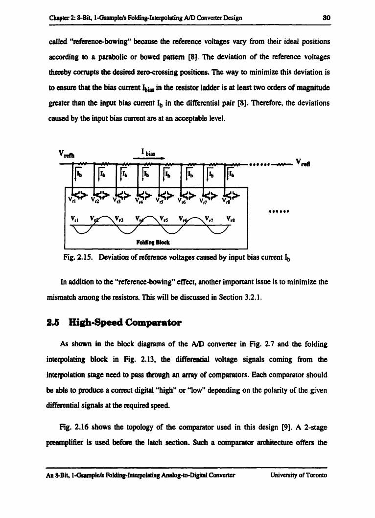
Chapter 2: %Bit, 1-GsampIJs Folding4nterpolating AD Converter Design 30
calkd "reference-bowing" because the nference voltages Vary from their ideal positions
according to a paraboIic or bowed pattern [8], The deviation of the nference voltages
thenby cormpts the desind zero~c~ossing positions. The way to minimize this deviation is
to ensure that the bias cumnt in the "stor lsdder is at least two or&n of magnitude
p a t e r than the input b i s cumnt b in the dintrential pair 181. Thenfore, the deviations
caused by the input bias cumnt are at an acceptable level.
Fig. 2.15. Deviation of nfemce voltages caused by input bias cumnt Ib
In addition to the "reference-bowing" effect, another important issue is to minimize the
mismatch among the mistors. This will be discussed in Section 3.2.1.
As shown in the block diagrams of the AiD converter in Fig. 2.7 and the folding
interpolathg block in Fig. 2.13, the diffenntial voltage signals coming fiom the
interpolation stage need to pas through an array of comparators. Each cornparator should
be able to ptoduce a correct digital "high" or "low" depending on the polarity of the given
di&nntial signais at the quired speed.
Fig. 2.16 shows the topology of the cornparator used in this design [9]. A 2-stage
pnrmplincs is Psed bfon the litch section. Such a comparaûot architecture offers the
-- -- -
An &Bit, I..GspinpWs Foldiag-InterpoIaihg Analwto-Digital Convertet University of Toronto
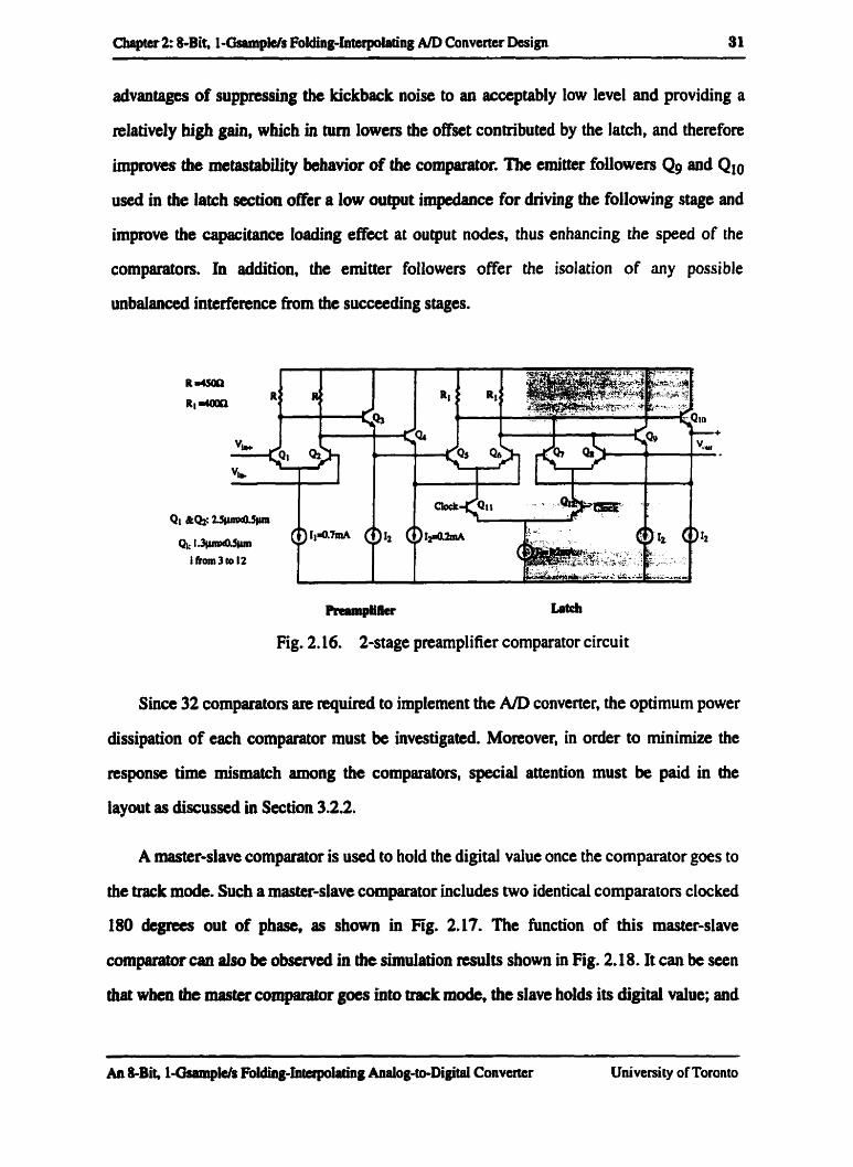
advantagcs of suppressing the kickback noise to an acceptably low level and providing a
relatively bigh gain, which in hm lowers the offset contnbuted by the latch, and therefore
impnms the rnetastability bchavior of ihe comparator. The emiüer followers Q9 and Qio
used in the latcb sectioa offer a low output impedance for &Wig the following stage and
improve the capitance IoPding effect at output nodes, thus enhancing the speed of the
comparators. Ia addition, the emitter followen offer the isolation of my possible
unbdanced intetference h m the sucatding stages.
Fig. 2.16. 2-stage preamplifier comparator circuit
Sincc 32 comparaton am requind to implement the ND converter, the optimum power
dissipation of each compamtor must be investigated. Moreover, in order to minirnize the
mponse time mismaich among the comparators, special attention must k paid in the
iayout as discussed in Section 3.22.
A master-slave comparator is used to hold the digital value once the comparator goes to
the üack mode. Such a mastcr-slave compamtor inchdes two identical comparators clocked
180 degrees out of phase, as shown in Fig. 2.17. The hinction of this master-slave
cornparatm can also be obsemd in the simulation results shown in Fig. 2.18. It can be seen
that when the master comparator goes hto tnck mode. the slave holds its digital vaiue; and
An &-Bit, L-Gsamplds Folding-Inicrpolating Analog-to-Digitai Converter University of Toronto
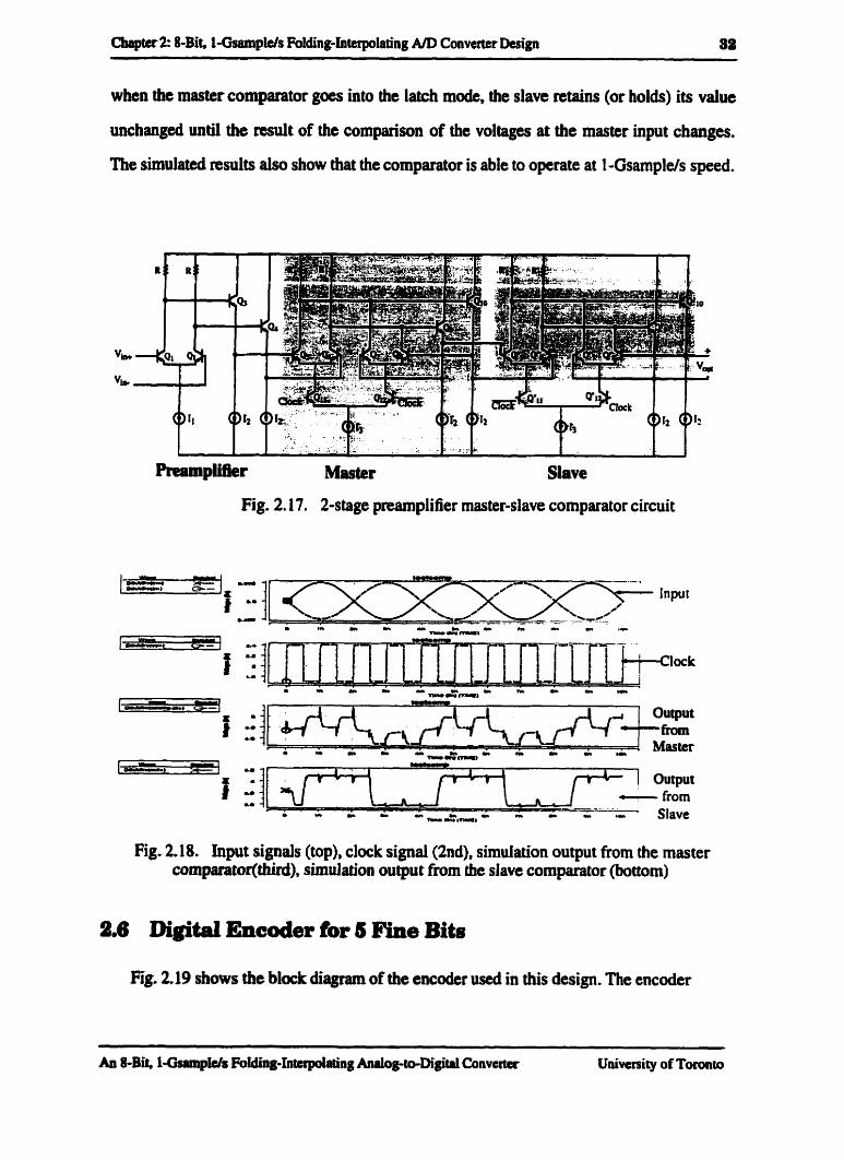
Chspt# 2: 8-Bit, 1-GsampW9 Folding-Inteplathg AlD Convater Design SB
when the master comparator goes into the latch mode. the slave retains (or holds) its valut
unchanged until the nsult of the cornparison of the voltages at the master input changes.
The simulatecl nsuits also show that the comparator is able to operate at 1 -Gsample/s speed.
Fig. 2.17. 2-stage preamplifier master-slave comparator circuit
Fig. 2.18. Input signais (top). clock signal (2nd), simulation output ftom the master comparator(third), simulation output from tbe slave comparator (bottom)
2.6 Digital Encoder for 6 Pine Bite
Fig. 2-19 shows the block diagani of the encoder used in ihis design. The encoder
An 8-Bit, 1-GsampWs Folding-IirterpoIating Anaiog-to-Digîtai Converter University of Toronto
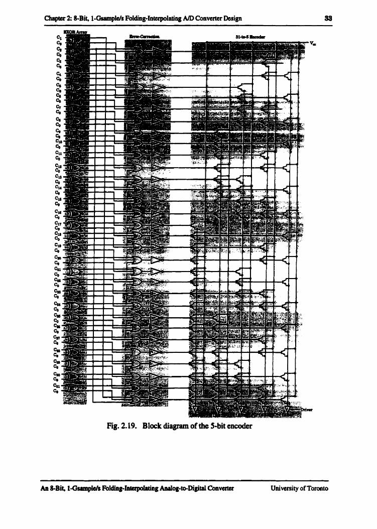
Chaptcc 2: 8-Bit, 1-ûsamplels Folding-Intetpolating A / ' Converter Design 33
Fig. 2.19. BIock diagram of the 5-bit encoder

comprises 3 huiction blocks. They are an Exclusive-OR (EXOR) amy, an emr comction
stage, ad a 3 1-to-5 encoàer. After the comparator stage, the digital combinations of 32
"ONE" and "ZERO" are obipineci. Such combinations must be encoded into a binary code.
Because of the repetitive nature of the folding signals. a circular code, instead of a
linear themiometet code, is obtained. Table 2.2 lis& the npnsentation of the numbers €rom
O to 7 using circular CO& and themorneter code respectively. When encoding such a
circular code, the transition between a group of ONE'S and a group of ZERO'S must be
defined h t . An EXOR operation is penormed to realize this transition [10]. Fig. 2.20
shows the configuration of such a diffenntiai EXOR circuit [SI. Minimum size transistors
are used to reduce the chip size. Fig. 231 shows the simulated results for the differential
EXOR gate.
liible 2.2 Thermometer and circular code repmentation of the numkrs 0-7
An &Bit, I-GsampI Js Folding-Inte~l&gAnaloEto-Di$ital Converter University of Toronto

Fig. 2.20. EXOR circuit
Fig. 2.21. Simulation output wavefonn h m the EXOR gate. ' h o inputs (Top), EXOR Output (Bottom)
After the EXOR stage, a themotneter-lile codes are obtained. An emr-comction
stage (OR gates and inverters) [8, LI] is used to comct any inconsistencies due to
compantm mtagtabiiity, noise and cross tallc. A 3 input OR gate is used in this design. The
themorneter codes mua ôe cncocIeâ into the cottcsponding 5-bit binary code. This is
accomplished by a 3 1-to-5 OR ROM encoder [IO] as show in Fig. 2.19. In the design of
the encoder, special attention is needed to achieve the required speed of each gate while
An %Bit, 1 -GssnipWs FoIding-Interpollrtibg Anal~~to-h'gital Converter University of Toronto
Chaptcr 2: Mit, I-GsampIe/s Folduig-Intupotating AID Convatet Design 36
using minimum power in order to k p the power consumption of the overall system as Iow
as possible.
8.7 The Coarse Quantber
The block diagram of the coasse quantizer is highlighted in Fig. 2.22. A buffer and a
comparator are utiiized to generatc the MSB. MSB-1 is produced by employing a folding
block with folding rate equd to 4 and a compuator. Fig. 2.23 shows the outputs fiom the
MSB-1 folding block. MSB-2 can be obtained directiy from the fine quantizer without
using any additional circuiüy.
Fia. 2.23. Simulation outputs h m MSB-I folding block
-- -
An Mit, I-GsampIds Folding-Interpolating Anaiogto-Didtal Convater University of Toronto
Chapter 2: &Bit, I-GsampI Js Folding-Interpolaîing AîD Converter Design 37
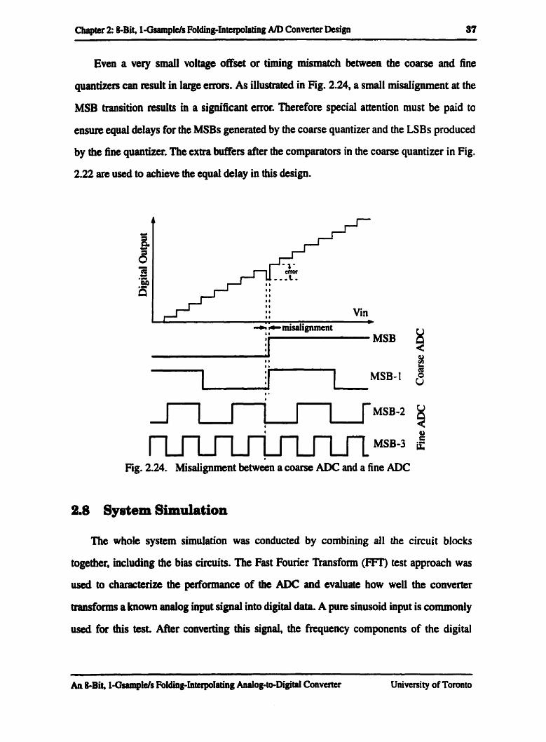
Even a very smd voltage offset or timing mismatch between the coarse and fine
quantizeis can result in large emrs. As iliusbptcd in Fig. 2.24, a smail misalignment at the
MSB transition results in a significant e m Therefore special attention must be paid to
ensure quai delays for the MSBs generated by the coarse quantizer and the LSBs produced
by the fine qumtizer. The extra buffiers after the comparators in the coarse quantizer in Fig.
2.22 an used to achieve the equal &lay in this design.
Vin
Fig. 2.24. Misalignment be&n a CO- ADC and a fine ADC
2.8 Syatem Simulation
The whole system simulation was conducted by combining dl the circuit blocks
together. including the bias circuits. The Fast Fourier Transfonn (FFT) test approach was
uscd to chorscterhe the pafotm8acc of the ADC and evaluate how well the converter
trmsforms a known analog input signai into digital dota A pure sinusoid input is commonly
used for thia test After converting this signai, the hquency componenis of the digital
An &Bit, L-Gsampl J s Foldhg-Interpotaihg Analo'to-Digital Converter University of Toronto
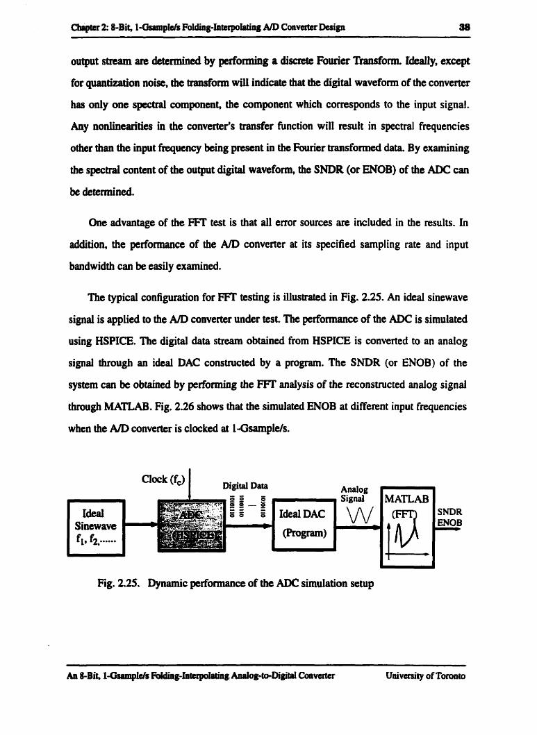
output stream are determined by performing a dimete Fourier Transfom. GdeaUy, except
for quantbation noise, the tmsform will indicate that the digital waveform of the converter
h a only one spectral component, the component which corresponds to the input signal.
Any nonlinearities in the converters tmsfer function will nsult in spectral frequencies
other than the input fkquency being pzesent in the Fourier transformeci data By exPmining
die specüai content of the output digital wavefom, the SNDR (or ENOB) of the ADC can
be detennined.
One advantage of the FFI' test is that ail enor sources are included in the results. In
addition, the performance of the A/D converter at its specified sampling rate and input
bandwidth can be easily examiaed.
The typical configuration for FFI' testing is iliustrated in Fig. 2.25. An ideal sinewave
signal is applied to the A/D converter under test. The performance of the ADC is simulated
using HSPICE. The digital data Stream obtained from HSPICE is converted to an analog
signal ihrough an ideal DAC constmcted by a program. The SNDR (or ENOB) of the
system cm be obtained by perfomiing the FFT analysis of the reconstnicted analog signal
through M A . . Fig. 2.26 shows that the simulated ENOB at different input fiequencies
when the A/D converter is clocked at 1-Gsamplels.
Digital Data
Fig. 2.25. Dyriamic performance of the ADC simulation setup
SNDR EN00 -
An &Bit, l-Gsamplds Fotduig-htcrpoIating Analog-to-Digitad Convater University of Tomnto
Chopter 2: 8-Bit. 1-Geomplels Foldùig-Interpoiating A/D Convcrter Design 39
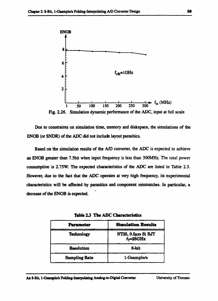
ENOB
Fig. 2.26. Simulation dynamic performance of the ADC, input at hiIl scaie
Due to constraints on simulation time, memory and diskspace, the simulations of the
ENOB (or SNDR) of the ADC did not include layout parasitics.
Based on the simulation resuits of the A/D converter, the ADC is expected to achieve
an ENOB greater than 7.5bit when input fnquency is less than 300MHz. The total power
consumption is 2.7x The expected characteristics of the AM3 are listed in Table 2.3.
However, due to the fact thnt the ADC o p t e s at very high frequency, its expenmental
characteristics will be affectcd by parasitics and component mismatches. In partidas, a d
decrease of the ENOB is expected.
'ïàbie 23 The ADC CbaracteWcs
1 Sampîing Rate 1 l-Gsamplels

a ibk 2.3 Tbe ADC CbriraccteristEcs
Signal Bandwidth
1 ENOB 1 7.7-bit
In this chapter, the architecture and design of the 8-bit, 1-Gsampleis folding-
interpo1ahg ND converter was described. The design of each individual circuit block in the
A/D converter was discussed. The simulation results for each of the circuit blocks and the
entire ADC were presented.
- -- -
An &Bit, l ~ I J s Foiding-uiterpoIottogAnalo~t0,Digi~ Convater University of Toronto
Cbapter 2= &Bit, 14sampIds Folding-Interpolating A(D Converter Design 41
References [1] B. Gilbert, 4'M~nolithic Analog READY-ONLY Memory for Characta Genetation,"
IEEE Jounial of Solid-State Circuits, vol. SC-6, pp. 45-55 197 1 .
[2] B. Giîbert, "A Monolithic Miaosystem for Analog Synthesis of Trigonometnc Func-
tions and Their Inverses," IEEE Journal of SolidState Circuits, vol. SC4 7 , pp. 1 179-
1I91,1982.
[3] R. J. van de Plassche and R E. J. van de Griît, "A High-Speed Fbit A D Converter,"
IEEE Joumal of Sotid-State Circuits, vol. SC- 14, pp, 938-943,1979.
[4] R. van de Grift and R S. van de Plassche, "A Monolithic 8-bit Video A/û Converter,"
IEEE Joumul of SolUI-Stute Circuits, vol. SC-19, pp. 374-378, 1984.
[s] EL Kobayashi. T. Tobari, H. Matsuura, A. Mura, M. Yamanaka, T. Yakihara, S. Koba-
yashi. S. Oka, T. Fujita and D. Murata. "System Architecture and Key Components of
Multi-Giga-Hertz A/D Converter with HBT," IEEE Instrumentation und Meusurernents
Techlogy Conrfmnce, Pmceedings, pp. 1 1 60- 1 166,1996.
[6] W. T. Colleran and A. A. Abidi, "A IO-b, 75MHz Tbvo-Stage Pipelined Bipolar A/D
Converter," IEEE Journal of Solid-State Circuits, vol. 28, pp. 1 187- 1 199, 1993.
[7] B. Nauta, A. G. W. Venes, "A 70-MS/s 1 IO-mW 8-b CMOS Folding and Interpolating
A/D Converter:' IEEE Joumd of Solid-Stute Circuits, vol. 30, pp. 1 302-1 308, 1 995.
[8] D. A. Johns and K. W. Martin, Analog Integrated Circuit Design. John Wiley & Sons.
Inc., Toronto, Canada, 1997.
[9] B. Razavi, Principles of Data Conversiofi System Design, IEEE Press, New York. 1 995.
[IO] R. J. vm de Plassche and P. Boltus, "An &bit lûûMHi Full-Nyquist Analog-to-Digitai
Converter," IEEE loumul of Solid-State Circuits, vol. 23. pp. 1334-1 344, 1988.
An 8-Bit, 1-GsampIds Fi,1dibg-laterpoIrting Analog-to-Digitai Convater University of Toronto

[ll]K C. Wang. P. M. Asbeck, M. P. Chang. G. J. Sullivan and D. L. Miller, "A 4Bit
Quantizer hplemcntcd with AlGaAs/GaAs Hetemjunction Bipolar Transistors," lEEE
GaAs lC Symposium, Technical Digest, pp. 83986,1987.
An &-Bit, l - C h ~ @ d s FoBdmg-TirterpoletingAaaloptO-Di@d Convertet University of Toronto
Cbaptcr 3: T b A/D Converter Implementation and Experimcntal Rcsuits 43
CHAPTER 3
The A/D Converter Implementation and Experimental Resuits
This chapter deals with the implementation and test of the ND converter designeci in
Chapter 2. Layout techniques used to acfiieve the requkd performance is discussed.
Experimental nsults verifying the fuactiondity and testing of the high fiequency
performance of the A D converter are also presented.
3.2 Layout of the AM:
The A D converter relies on the layout to meet the strinpnt quimnents on speed and
cesolution of the design. An appropriate layout not only maximizes the yield but also is the
only way to achieve the required specifications predicted by simulations. Special attention
was given to the component rnatching, and wiring of signal and dock paths. Since the ADC
is a mUed-signai circuit, issues nlated to the noise-rejection were also considemi.
1 Component matching
Component matching is important in anaiog circuits. In ptactical situations there will
be mismatches among componeuts which are intended to be identical. Mismatches
adversely affect the îinearity and accuracy of the converter. Mismatches in the input
di&rential transistor pairs within the folding circuits and the pre-ampiifiers in the

Chapter 3: The A/D Converter Implemcntation and Expetimtntai Resuïts 44
cornparators, and mismatches between the cross-coupled latches cm cause sipificant offset
enws. Special layout techniques must be used to improve the mtching among these
transistors. This includes the use of the common-centmid approach and the use of United
cells comected in pandiel for large objects.
Another important issue is the layout of the refecence ladder and the resistive strings in
the interpolators. The absolute value of the individual resistor is not important but the ratios
of the resistors in the ladder and strings an aiticai. If all the individual resistors change by
the same amount, the nference voltages can remain the same and equal interpolation cm be
retained. Therefore, carefd consideration must be given to keeping the ratio of resistors
uncbanged. Using a common-centmid and psrallel connected uniteci ceil approaches,
maintaining the same contact configuration and layout orientation for each resistor are
requireà. In addition, "dumrny resistors stipes" must be added to the extnmities of the
resistor stripes.
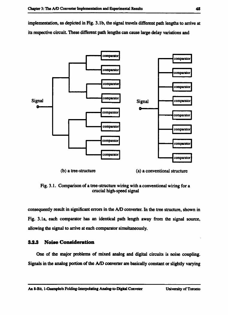
83.2 Clocit and Signal Path Layout
The low fnquency accuracy of the A D converter is lirnited by comparator offsets
causeci by parameter mismatches. However, at high frcsuencies, the accuracy of the
converteî- dccrcases maialy due to timing mismatches among comparators, which make the
comparators simple values of the input signal at Mennt times. These timing mismatches
originate fiom clifferences in the amival of the clock and input signal to their respective
circuitry. In this design, the comparator anay consists of 32 cornparators. The timing
mismatches must be mlliimizeâ to met the speed and nsolution required because the
converter ha9 to operate at 1-Gsamplds with a nsolution of 8-bit. To minimize the timing
mismatches, the wUUlg for each of the dock and signal paths in the layout must be highly
symtnetricai. Therefore a tree-stnicture is used for the layout of the clock and analog signal
paîhs in this design. The conœptuai diagram is pmsented in Fig. 3.1% In a conventionai
An &Bit, 1 -GsamplJs Folding-fntcrpoIating Amiog-to-Digitai Cmveter University of Totonlo
Chripter 3: Tbe A/D Convater Implementaîion and Experimental Results 46
implemcntation, as d e p k d in Fig. 3.lb. the signai travels different path leogths to arrive at
its respective circuit. These diffemnt path lengths cm cause large &Iay variations and
Signal
comparatot r=
comparator t--= comparator a
(b) a ûee-structure (a) a conventional structure
Fig. 3.1. Cornparison of a tree-structure wiring with a conventional wûing for a cruciai high-speed signal
consequentiy result in significant emrs in the N D converter. In the tne structure, shom in
Fig. 3.1% each comparator has an identical path length away h m the signal source,
ailowing the signal to arrive at each comparator simultaaeous1y.
One of the major problems of mixed analog and digital circuits is mise coupling.
Signds in the anaiog portion of the A/D converter are bas idy constant or sligbtly vorying
Chaptcr 3: Tûe AD Converter ImpIune~~tati*~~~ anci Eqcdmcntal Rcsuiîs 46
in thne while signal in the digitai portion of the ADC consists of changing pattern of puises.
Consequently any noise generated in the digital section of the ADC is coupled into the
andog circuits through the powet supply and the substrate. Routing an analog signal
parallel to a digital line aIso resuits in a capacitive coupling bctween two iines.
To avoid the digital noise or cross-talk over the power supply connections, separate
power supply ihes and pins are used for the digital and anaiog sections. Monover. separate
power supply is used for digital output cirivers since it has to handle large curent spüces.
To minimut the noise coupling through the substrate, the analog portion is physicaily
separated from the digital portion by g w d rings and wells [l]. Shieldiag layen are also
used to d u c e capacitive coupling between the circuit elements. For example. an n-layer is
put undemeath the nsistors, capcitors and clock buses [2].
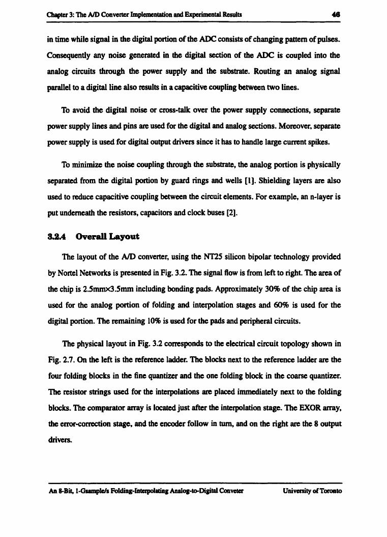
The layout of the A/D converter, using the NTZS silicon bipolar technology provideci
by Norte1 Netwotks is presenteâ in Fig. 3.2. The signal flow is from left to right. The ana of
the chip is 2.5mmx3.5mm including bonding pads. Approximately 30% of the chie ana is
used for the analog portion of folding and interpolation stages and 60% is used for the
digital portion. The remauUng 10% is used for the pads and peripheral circuits.
The physicai layout in Fig. 3.2 conesponds to the electrical circuit topology show in
Fig. 2.7. On the left is the reference ladder. The blocks next to the refennce ladder are the
four folding blocks in the fine quantizer and the one folding block in the coarse quantizer.
The resistor strings used for the interpolations are placed immediately next to the folding
blocks. The compamtor array is located just aftcr the inteplation stage. The EXOR amy,
the eiror-correction stage, and the encoder foliow in tum, and on the right are the 8 output
cirivers.
Cbapter 3: The AîD Convertu Implemntation and Experimtntai Results 47
Signal flow ,-b
anaiog portion digital portion (-m
I clocktree 1 signal tree
guard rings and weUs
Fig. 3.2. Layout of the ADC using the NT25 technology
An important issue in the layout involves ensuring correct metal widths to m a t the
cumnt density nquirements in ail the metal layers and having enough contacts and vias to
han& the currtnt going thn,ugh various interconnections. The metai ünes mtllljng
vertidy in Fig. 3.2 arc power liaes whidi need to be wide cnough to meet current density
requinments. Also, metai layes are useci for comections as much as possible to keep
interconnect resistance and delay low. Ccossing between metai lines is kept to a minimum.
8.8 The A/D Converter Implementatîon
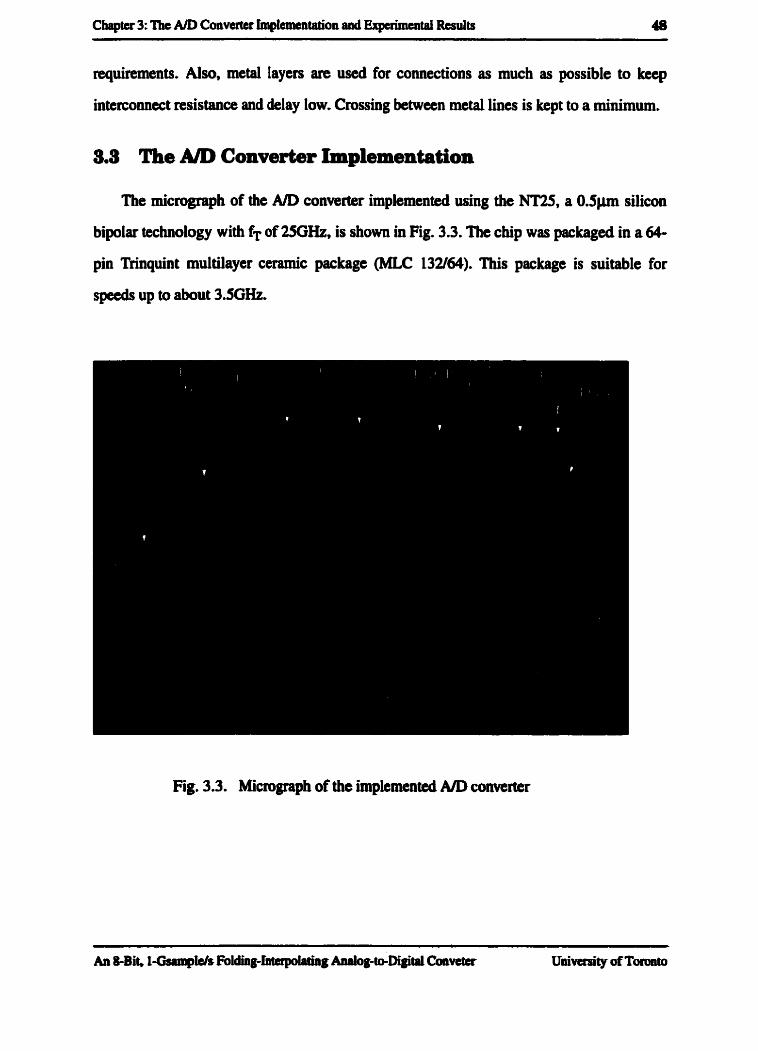
The micmgraph of the A/D converter implemented using the NT25, a 0 . 5 ~ silicon
bipolar technology w ith fT of ZSGHz, is shown in Fig. 3.3. The chip was packaged in a 64-
pin Tnnqu.int multüaycr ceramic package (MU: 132f64). This package is suitable for
speeds up to about 3.5Gk.
Fig. 3.3. Mimgraph of the implementcd N D convcrtcr
Cbapter 3: The A/D Converter Inspl~~~~ntation and Expdmcntal Results 49
The packaged AID convertcm were evduatcd and tested for full speeâ using the
Triquint's ETF-MLC 132/64 test kture. In tbis test fixtun, a heat si& incorporated into
one of the retainer aîsemblies provides efficient cwling, and capacitive decoupling is also
pmvided for chip power supplies.
By enswing appropriate bias conditions and teference voltages, the static and dynamic
perfomance of the A/D converter were tested. In the static test the fiuictionality of the A/D
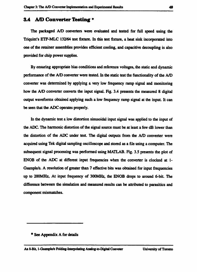
converter was determineci by applying a very low fnquency ramp signal and monitoring
how the A/D converter converts the input signal. Fig. 3.4 prwents the measunxi 8 digital
output wavefonns obtained applying such a iow frequency ramp signal at the input. It can
be seen that the AM3 operates properly.
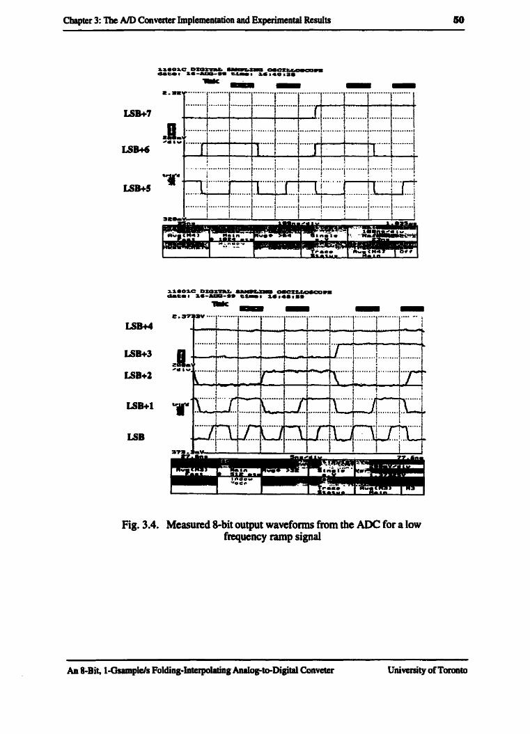
In the dynamic test a low distortion sinusoidal input signal was applied to the input of
the ADC. The hannonic distortion of the signal source must be at least a few dB lower than
the distortion of the ADC under test. The digitai outputs from the A/D converter were
acquired using Tek digital sampling oscilioscope and stored as a file using a computer. The
subsequent signal pmcessing was performed using MATLAB. Kg. 3 5 presents the plot of
ENOB of the ADC at dinereat input frrquencies when the converter is clocked at 1-
Gsample/s. A nsolutioa of greater than 7 effective bits was obtaiaed for input fnquencies
up to 2OOMH2, At input frcsucncy of 300- the ENOB drops to around &bit The
differenœ between the simulation and rneasurcd resuits can be attributcd to parasitics and
component mismatches.
* Sœ Appendix A for &rails
Cbapter 3: T b A/D Converter Implementation and ExpuimentaL Results 60
Fig. 3.4. Measund 8-bit output wavefom h m the ADC for a low fkquency ramp signal
An &Bit, I-OsampIels Folding-IntcrpoIathg Analog-tu-Digital Convctcr University 0fTomt0
Clraptcr 3: Thc AID Converter ImpIementation and Exptrimcntai Rcsults 61
ENOB
Simulation Measurement
Fig. 3.5. Measund dynamic perfomuuice of the ADC, input at fûil sa le
Eight packaged N D converters w e n tested. No significant diffennce in performance
was noted. Table 3.1 summarizes the characteristics of the %bit, 1-Gsamplds fdding-
interpolaihg AID converter.
'L1ibie 3.1: M e ADC perlonasnce
0.6pm Si BJT e 2 5 G H z
An &Bit, I-Gssri3pIe/s Foiâing-Inteipoiating Anaiog-to-Digitai Canveter University ofTomta
Signal Bandwidth
ENOB
200MHz
7.4bit
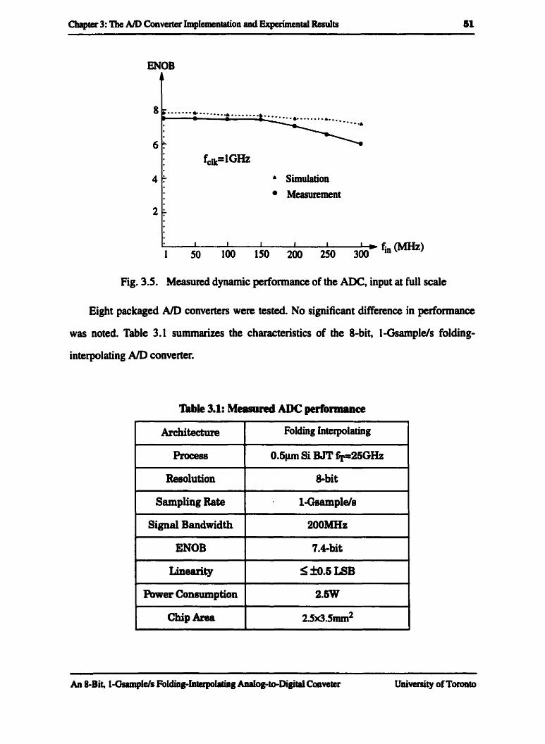
Chapter 3: The A/D Convertcc ImplementPtion and Experimcntai Results 52
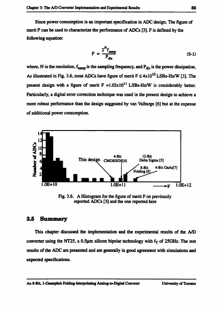
Since power consumption is an important specification ia ADC design. The figura of
ment F can be used to characte& the penonnance of ADCs [3]. F is defiaed by the
followiiig equation:
when, N is the molution. fMp is the sampüng fnquency, and Pdir is the pwer dissipation,
As iilustrated in Fig. 3.6. mosi A D 0 bave figure of ment F S 4 x 1 0 ~ ~ LSBs-HzW [3]. The
present &si@ with a figure of merit F -1.02~10" LSBs-Hz/W is considerably better.
Particularty, a digital emr correction technique was used in the present design to achieve a
more robust performance than the design suggested by van Vdburge 161 but at the expense
of additional power consumption.
Fig. 3.6, A Histograrn for the figure of merit F on previously reporteci ADCs [3] and the one nported hem
3.1 Summary
This chapter discussed the implementation and the experimental nsults of the A/D
converter using the NT25, a 0 . 5 ~ siiicon bipolar technology with fT of 25GHz. The test
mlts of the ADC are pttscntcd and are genemily in good agreement with simulations and
expected specificatioas.
Chapter 3: The A/D Converter Implcmntation and Exprimental b u l i s US
References [1] D. A. Johns and K. W. Martin, h b g Integrated Ciricuit Design, John Wilcy & Sons,
Inc., Toronto, Canada, 1997.
[2] N n S ElectnCaL Spec@cations and Loyout Design Rules, Vèrsion lS01.2 CMC, June
27, 1997.
(31 R. H. Wdden, "Analog-to-Digital Converter Technology Cornparison," IEEE GaAs IC
Symposium, Technicul Digest, pp. 217-219,1994.
[4] R H . Walden, AB. Schmitz, A.R. Krarner, L. E. Larson and J. Pasiecmilr, "A Deep
Submicrometer Analog-to-Digital Converter using focused-Ion-Bearn implants," IEEE
Journal of Solid-State Cimuits, vol. 25, pp. 562-57 1,1990.
M B. P. Brandt and B. A. Wooley, "A Sû-MHz Multibit Sigma-Dalta Modulator for 12-8
2-MHz A/D Conversion," IEEE Journal of Solid-State Cimuits, vol. 26, pp. 1746-
1756,1991.
[q 1. van Valburg and R. J. van de Plassche, "An 8-b 65@MHz Folding ADC," IEEE Jour-
nul of Solid-State Circuits, vol. 27, pp. 1662-1666, 1992.
[7] T. hicourant, M. Binet, J-C Baelde, Ch. Rocher and J-M Gibereau, "3 GHz lSOmW, 4-
bit GaAs Analog-to-Digital Converter," IEEE GaAs IC Symposium, Technicul Digest,
pp. 209-21 1, 1986.
An &Bit, l-GsampIJs Foidh~hterpolloting Analog-t0,Digital Convetcr University ofTomnto
Cbaptct 4: Conclusions 61
Conclusions
Tbis work was motivated by the demand for high-speed, hi&-nsolution analog-to-
digital converten for applications in direct IF sampling nceivers for wideband
communications systems. The use of silicon bipolar process for this work is aimed ai
integrating a Gsampleh ADC with a DSP system usually realized using a BiCMOS process.
The folding-interpdating architecture used in this work overcomes the drawbacks
associateci with paralle1 and feedforward architectures. Folding-interpolating converters
offer an optimum solution for Gsample/s. high-resoiution ADCs in terms of complexity,
power dissipation and chip area
A monolithic 8-bit, l-Gsample/s folding-interpolating A/D converter was designed and
impiementcd using the NT25. a 0.5 pm self-aügned, double polysilicon bipolar process
with maximum unity gain cutoff hquency fT of 25Gk. The N D converter consists of a
reference ladder; four folding blocb for the fine quantizef and one foIàing block for the
coarse quantizer, interpolation resistive strings; a comparator array; a digitai encodcr
including an EXOR amy, an emr-correction stage, and a 31-to-5 OR ROM; and a coarse
puantuer.
In order to achieve the cequiad specitications predicted by simulations and maximize
the yield of the &si@, special layout îechniqges were employed in the layout of the ADC

Chaptcr 4: Conclusions bb -- -
The experimental resuits of the AID converter show that it is capable of working to 1-
Gsamplds and achieving better than 7-bit ENOB when input signal fiequency is less than
2ûûMHz. nie maximum power dissipation of the ADC is 2.W and the chip ara is
2.5mmx3 .Smm
F u m work should f m s on reducing the power conmption and chip m a by
minimin'ng the power dissipation h m the comparators and the digital encoder. To improve
the performance when the input frequency is above 2ûûMHz. a S/H circuit can be added to
the ADC.
ND Converter Testing
In this appendix, the testing rnethodology used to characterize the performance of the
A/D converter is described. The discussion focuses on the dynamic test of the ADC.
Al Teeting Methodology
Severai analysis techniques enable characterization of an A D converter perfomance
based on collecting digital output data taken from the converter under test in nsponse to a
known input signal. In paRicular. performing a Fast Fourier Transfonn (FFI? on digitized
waveforms generates the ADC's digital output spectrum From which SNR. SNDR and
ENûB can be ascertaineci [1,2].
m e n an ided sinusoidai input signal of a known fkequency is fed through an ideal
?\DC, the FFT perfomed on the coliected digital data results only in the fnqueacy that
comsponds to the input fnquency, as ilhsüated in Fig. A. la
When a converter is not ideai and has nonlinearities, the input signal is distoctecl during
the conversion process. The resuIting FFL' has hannonics and a higher than ideal noise floor
as shown in Fig. AJb. The relationship between these harmonies, the noise flwr and the

Appendur A: Tbe ND Convuîcr Tcst 57
fundamental are used to specify the performance of the AIX. The ENOB of the converter
cm be obtained usiiig the foliowing equation:
signal ) - 1.76 ENOB =
6.02
A hput
Amplitude 4 , Fundamentai Prequency
Quantization Noise 1 1 1 1 1 1 1 1 1 1 1 1 1 1 1 1 1 1 1 1 1 1 1 1 1 , f
fin (a)
Fig. A.1. (a) FFI' of a pure sine wave with an ideal converter, (b) FFI' of a pure sine wave with a nonideai converter
Amplitude "
--- -
An 8-B& I-OarampWs Fddiag-Intcrpolating Anaiog-~Digitd Convater University of Toronto
Fundamental Frequency
7"i" Quantization Noise
L l l l I I I 1 1 1 1 1 1 1 1 1 1 1 1 1 1 ,f

Appendi. A: nie AID Converter Test 58
The Fa test directly evaluates how well the converter transfonas a known analog
signal into digital data. ûne advantage of this test method is that dl error sources are
included in the rwnilts. In addition, the performatlce of the A/D converter, at its speciAed
sampliag rate and input bandwidth, CM be e d y examined. This is the method used in this
work.
A9 Test Setup and Procedure
The test equipment used for characterizhg the performance of the AID converter
includes DC power supplies, a Rohde & Schwarz signal generator, a Colby PG3000A pulse
generator, a Tek 11801C digitai sampiing oscilloscope, and a personal cornputer. The test
setup is shown in Fig. A.2.
Colby Rilse Generator
Computer
Tek 1 1801C
Control DSO
Fig. A l AD converter test setup
Appcndix nie A/D Converter Test 59
The analog and digital power are pmvided by the DC power supplies. A Iow distortion
smusoid input with proper DC offset g e n e d by Rohde & Schwarz signal generator is fed
to the AM3 undet test. The clock driving signal is generated by the Colby PG 3000A pulse
generator. The digital output h m the ADC under test is monitored usiag Tek1 1801C DSO.
A personal cornputer is c o ~ e c t e d through the GBIP data bus of the DSO to collect the
digital output data. This data is then stored as a file on the harddisk for subsequent
pmcessiag. The FFT spectm analysis is p e r f o d on the output digital wavefom ushg
MATLAB, the corresponding ENOB (or SNDR) of the ND converter c m be therefore
obtained.
Appeudix A: Tbe ND Converter Test 60
References [il J. Doemberg, H. Lee, and D. A Hodges, 'FulI-Speed Tcsting of AiD Converters," IEEE
J o u d of SolidSute Circuits, vol. SC-19, pp. 820-827, 1984.
[2] T. E. Linnenbrink, '%ffkctive Bits: 1s That al1 There is?," IEEE T~llsactiun on Illsfru-
mentation d Measumment, vol. IM-33. pp. 184- 187.1984.
An &Bit, I-Gsanyrlds Foidhg-Inoerpolating Analog-t0,Digital Convater UniYCtSity of Toronto
Related Documents