Algorithmic Design Methodologies and Design Porting of Wireline Transceiver IC Building Blocks Between Technology Nodes S.P. Voinigescu, T.O. Dickson, T. Chalvatzis, A. Hazneci, E. Laskin, R. Beerkens*, and I. Khalid* Edward S. Rogers Dept. of ECE, University of Toronto, 10 King's College Rd., Toronto, ON, M5S 3G4, Canada *) STMicroelectronics, 16 Fitzgerald Rd., Ottawa, Ontario, K2H 8R6, Canada Abstract-This paper presents an analysis of sub-2.5-V topologies and design methodologies for SiGe BiCMOS and sub-90nm CMOS building blocks to be used in the next generation of 40-100 Gb/s wireline transceivers. Examples of optimal designs for 40-80Gb/s broadband low-noise input comparators, low-voltage high-speed MOS- and BiCMOS CML logic gates, 30-100 GHz low-noise oscillators, and 40/80 GHz output drivers with wave shape control are provided. I. INTRODUCTION As the data rates of broadband communication systems continue to increase, noise generated inside the circuit becomes a critical component in limiting the sensitivity of wide-band input stages for building blocks such as A/D converters, equalizers, and decision circuits. With each new technology generation, this situation is further exacerbated by the trend towards lower supply and breakdown voltages, yet another reason for dynamic range and link reach degradation in wireline data transmission. At the transmitter end, being able to provide maximum swing with adjustable wave shape to compensate for package, backplane and connector loss and reflections at data rates beyond 10 Gb/s has become a critical requirement in extending the reach of wireline communication systems. As supply voltages are lowered, the number of transistors that can be stacked in a circuit topology must also be reduced without compromising performance. To make up for the limited flexibility of low-voltage circuit topologies, optimal transistor sizing and biasing for low-noise, adjustable output swing, and broadband switching will play an even more dominant role in high-performance circuit design. It becomes increasingly important to re-examine the suitability of commonly deployed low-noise broadband amplifier and VCO topologies for applications beyond 40 Gb/s. Finally with the migration of large digital chips to prohibitively expensive 90- nm and 65-nm CMOS-only technologies, it is likely that, to remain economically viable, 40-Gb/s or 80-Gb/s transceivers will simply evolve into re-usable IP blocks on a large digital die. This scenario points to the importance of developing algorithmic design and IP porting methodologies for high- speed digital and broadband CMOS building blocks from one technology node to the next. Fig. 1 shows that the measured maximum available power gain of single-transistor and cascode stages fabricated in state- of-the-art SiGe BiCMOS and 90-nm CMOS technologies rises above 8 dB at 65 GHz. Taking advantage of this outstanding transistor performance, we have recently demonstrated large levels of integration at 80 Gb/s in a PRBS generator with 2 31 -1 pattern length, implemented in 130-nm SiGe BiCMOS technology and operating from 3.3-V supply [1]. In this work, we revisit CMOS, SiGe HBT, and SiGe BiCMOS high-speed and low-noise circuits in the context of deep submicron technologies and of operation from 2.5 V or lower supply voltages. Our goal is to prove that all the building blocks for a sub 3-W transceiver, featuring at least 30 dB dynamic range and operating at 40 Gb/s or 80 Gb/s, are realizable in state-of- the-art silicon technologies. Therefore, the focus of the paper is on optimizing the key building blocks that limit dynamic range: input comparators, VCOs and output drivers. In Section II, analytical noise models are derived for CMOS and SiGe HBT broadband amplifiers. For the first time, an algorithmic low-noise design methodology for broadband preamplifiers is described and verified experimentally in a 130-nm SiGe BiCMOS process. Experimental results on 40-Gb/s preamplifiers in SiGe BiCMOS technology are discussed and compared with simulations of 90-nm, and 65-nm CMOS-only TIAs that are currently in the fab. In Section III, we compare CMOS, MOS-CML and BiCMOS-CML logic gates. A simple methodology is proposed for the design of MOS- and BiCMOS-CML digital gates. It relies on the invariance of the peak fT current density between foundries and technology nodes [2], on the self- resonant-frequency x inductance (SRF*L) product of a given semiconductor process, and on minimizing voltage swing [3]. Fig. 1. Measured maximum available power gain for SiGe HBTs, 90-nm n- MOSFETs, 130-nm HBT-MOS (BiCMOS), and 90-m MOSFET cascodes.

Welcome message from author
This document is posted to help you gain knowledge. Please leave a comment to let me know what you think about it! Share it to your friends and learn new things together.
Transcript
Algorithmic Design Methodologies and DesignPorting of Wireline Transceiver IC Building Blocks
Between Technology Nodes S.P. Voinigescu, T.O. Dickson, T. Chalvatzis, A. Hazneci, E. Laskin, R. Beerkens* , and I. Khalid*
Edward S. Rogers Dept. of ECE, University of Toronto, 10 King's College Rd., Toronto, ON, M5S 3G4, Canada * ) STMicroelectronics, 16 Fitzgerald Rd., Ottawa, Ontario, K2H 8R6, Canada
Abstract-This paper presents an analysis of sub-2.5-Vtopologies and design methodologies for SiGe BiCMOS andsub-90nm CMOS building blocks to be used in the nextgeneration of 40-100 Gb/s wireline transceivers. Examples ofoptimal designs for 40-80Gb/s broadband low-noise inputcomparators, low-voltage high-speed MOS- and BiCMOSCML logic gates, 30-100 GHz low-noise oscillators, and 40/80GHz output drivers with wave shape control are provided.
I. INTRODUCTION
As the data rates of broadband communication systemscontinue to increase, noise generated inside the circuitbecomes a critical component in limiting the sensitivity ofwide-band input stages for building blocks such as A/Dconverters, equalizers, and decision circuits. With each newtechnology generation, this situation is further exacerbated bythe trend towards lower supply and breakdown voltages, yetanother reason for dynamic range and link reach degradationin wireline data transmission. At the transmitter end, beingable to provide maximum swing with adjustable wave shape tocompensate for package, backplane and connector loss andreflections at data rates beyond 10 Gb/s has become a criticalrequirement in extending the reach of wireline communicationsystems. As supply voltages are lowered, the number oftransistors that can be stacked in a circuit topology must alsobe reduced without compromising performance. To make upfor the limited flexibility of low-voltage circuit topologies,optimal transistor sizing and biasing for low-noise, adjustableoutput swing, and broadband switching will play an even moredominant role in high-performance circuit design. It becomesincreasingly important to re-examine the suitability ofcommonly deployed low-noise broadband amplifier and VCOtopologies for applications beyond 40 Gb/s. Finally with themigration of large digital chips to prohibitively expensive 90-nm and 65-nm CMOS-only technologies, it is likely that, toremain economically viable, 40-Gb/s or 80-Gb/s transceiverswill simply evolve into re-usable IP blocks on a large digitaldie. This scenario points to the importance of developingalgorithmic design and IP porting methodologies for high-speed digital and broadband CMOS building blocks from onetechnology node to the next.
Fig. 1 shows that the measured maximum available powergain of single-transistor and cascode stages fabricated in state-of-the-art SiGe BiCMOS and 90-nm CMOS technologies risesabove 8 dB at 65 GHz. Taking advantage of this outstanding
transistor performance, we have recently demonstrated largelevels of integration at 80 Gb/s in a PRBS generator with 231-1pattern length, implemented in 130-nm SiGe BiCMOStechnology and operating from 3.3-V supply [1]. In this work,we revisit CMOS, SiGe HBT, and SiGe BiCMOS high-speedand low-noise circuits in the context of deep submicrontechnologies and of operation from 2.5 V or lower supplyvoltages. Our goal is to prove that all the building blocks for asub 3-W transceiver, featuring at least 30 dB dynamic rangeand operating at 40 Gb/s or 80 Gb/s, are realizable in state-of-the-art silicon technologies. Therefore, the focus of the paperis on optimizing the key building blocks that limit dynamicrange: input comparators, VCOs and output drivers.
In Section II, analytical noise models are derived forCMOS and SiGe HBT broadband amplifiers. For the firsttime, an algorithmic low-noise design methodology forbroadband preamplifiers is described and verifiedexperimentally in a 130-nm SiGe BiCMOS process.Experimental results on 40-Gb/s preamplifiers in SiGeBiCMOS technology are discussed and compared withsimulations of 90-nm, and 65-nm CMOS-only TIAs that arecurrently in the fab.
In Section III, we compare CMOS, MOS-CML andBiCMOS-CML logic gates. A simple methodology isproposed for the design of MOS- and BiCMOS-CML digitalgates. It relies on the invariance of the peak fT current densitybetween foundries and technology nodes [2], on the self-resonant-frequency x inductance (SRF*L) product of a givensemiconductor process, and on minimizing voltage swing [3].
Fig. 1. Measured maximum available power gain for SiGe HBTs, 90-nm n-MOSFETs, 130-nm HBT-MOS (BiCMOS), and 90-m MOSFET cascodes.
This methodology also allows to port and scale designs easilyfrom one foundry to another and between CMOS/BiCMOSgenerations. Next, an analysis of mm-wave CMOS and SiGeBiCMOS VCOs is carried out in Section IV. Finally, SectionV looks ahead to the International Technology Roadmap forSemiconductors (ITRS) time horizon [4] in an attempt toovercome the problem of data and clock transmission over 5-cm long on-chip interconnect. The first 2.5-V, 80-GHz driverwith pre-emphasis control is described and characterized.
II. LOW-NOISE BROADBAND INPUT COMPARATORS
At lower data rates, issues related to reflections from poorPCB tracesand connectorsdominate backplane or chip-to-chiptransceiver performance. Beyond 10 Gb/s, circuit noise itself,integrated over increasingly larger bandwidths, becomes yetanother limiting performance factor, raising the need for low-noise input stages. The noise of a two-port network is usuallymodeled in terms of two input-referred correlated noisesources <vn
2> and <in2>. The correlation between these noise
sources can be captured using an admittance formalism, inwhich case the noise in the network is completely described bythe correlation admittance YCOR, the noise conductance Gn, andthe noise resistance Rn [5], or employing an impedanceformalism, which gives rise to an equivalent set of noiseparameters zcor, rn and gn. The minimum noise factor FMIN isobtained for a unique optimum source admittance YSOP = zsop
-1.For clarity, noise parameters in the impedance and admittanceformalisms are denoted throughout this work by lower-caseand upper-case letters, respectively. The impedance formalismis convenient for analysis of noise in circuits with seriesfeedback while shunt feedback is more readily investigatedusing the admittance formalism.
A series-series feedback circuit, such as the resistivelydegenerated INV in Fig 2(a), can be described by the sum ofthe two-port Z-parameter matrices of the forward amplifierand the feedback network, namely Z = ZA + ZF. Assuming thatthe forward amplifier is nearly unilateral and that its forwardtransmission dominates that of the overall network, it can beshown that the optimum source impedance of the feedbackamplifier is expressed in terms of the noise parameters of theforward and feedback networks as
z SOP r SOPA
2 r NF
g NA
2 r CORA Z 11F 2 Z 11F z CORF Z 11F 2 gNF
gNA
j X SOP Z 11F (1)
Here, subscripts ending in A and F refer to the noiseparameters for the forward amplifier and feedback network,respectively. The minimum noise factor of the overallamplifier is
F MIN 1 2g NA r CORA
r SOP Z 11F (2)
Likewise, shunt-shunt feedback systems such as the TIAsin Figs. 2(c), 3(b) and 3(c) can be analyzed using the Y-parameters and admittance-formalism noise parameters of theforward amplifier and feedback network. Similar assumptions
are made about the forward amplifier and feedback network aswere made for the series-series case, such that Y21 = Y21A andY12 = Y12F. The optimum source admittance and minimumnoise factor can be derived.
Equations (1)-(4) indicate that transimpedance feedbacklowers zSOP and is therefore useful when zSOPA is higher thanthe generator impedance. Since the zSOP of a transistordecreases with increasing size, bias current, and operationfrequency [6], it follows that, by using shunt feedback fornoise impedance matching, the size and bias current of theinput transistor will be smaller than in other topologies andthus lead to lower power dissipation and broader bandwidth.
Y SOP GSOPA
2 GNF
R NA
2GCORA Y 11F 2 Y 11F Y CORF Y 11F 2R NF
R NA
j B SOP Y 11F (3)
F MIN 1 2R NA GCORA
GSOP Y 11F (4)
It is important to note that the CMOS inverter of Fig. 3(c)can be analyzed as a composite transistor with twice thetransconductance per bias current, 2/3 times the fT, and 3/2times the (FMIN – 1) of the n-MOSFET of identical gate-length[3]. It becomes apparent that, if the fT is adequate for theapplication, the CMOS inverter will require half the size andbias current of an n-MOSFET fabricated in the sametechnology node to achieve a certain noise resistance andoptimum noise impedance with only a relatively smalldegradation of the noise figure [7]. This surprisingly little-known property of the CMOS inverter can significantly reducethe notoriously large power dissipation of noise-matchedtuned and broadband MOS low-noise amplifiers, especiallybelow 10 GHz [8].
Based on the preceding discussion, the INV, EF-INV, andTIA amplifiers of Figs. 2 and 3 are investigated to determinethe best topology for high-bandwidth low-noise amplifiers.The noise factor of the INV in Figs. 2(a) and 3(a) as a functionof the source impedance Z0 is given by
F Zo 1 1
1 L0
Z 0 2 Z 0 R N Y COR
2Z 0 2 GN
(5)
Noting that the noise parameters of the transistor RN, GN,and YCOR scale with the emitter length/gate width [6], one can
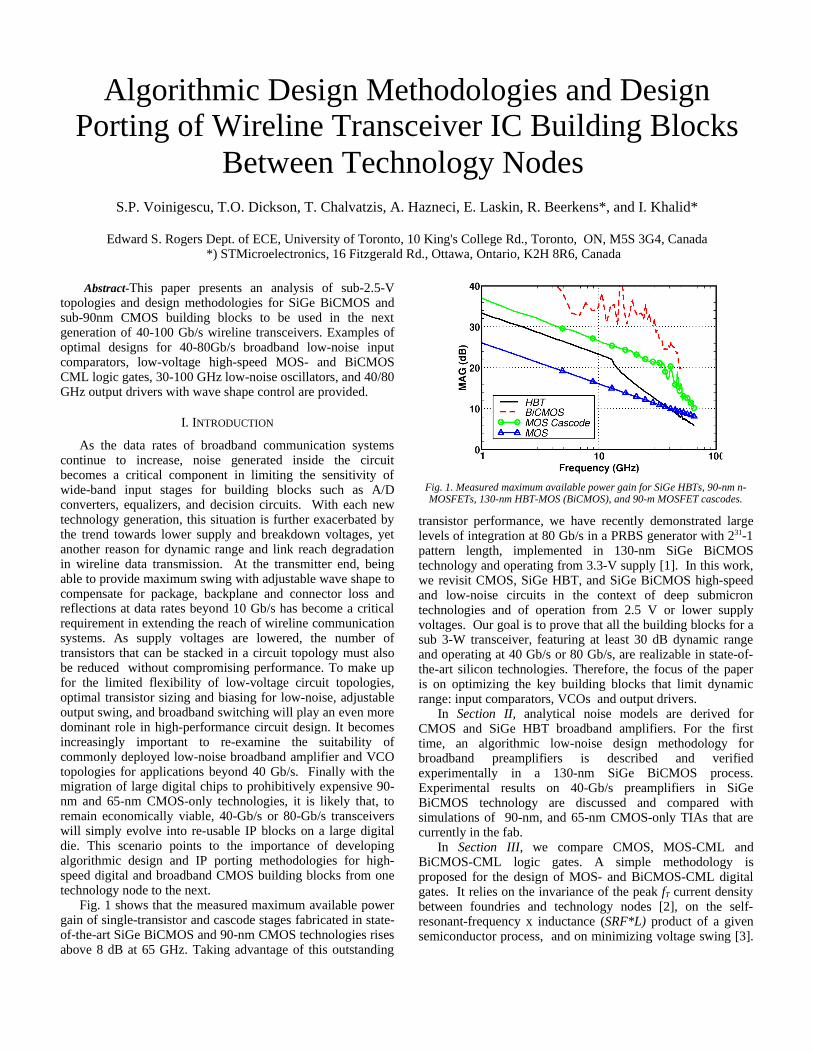
Fig. 2 SiGe HBT-based a) INV, b)EF-INV, and c) TIA inputcomparators.
RCZ0
L0 LC
RE
Q1
VOUT
VIN
VCC
Z0
L0
RC
LC
Q2
VOUTVIN
VCC
Q1 VOUT
VCC
RFLF
RC
LC
Q2
VIN
Q1

determine an optimal emitter length /gate width lEOPT /WEOPT
such that the right-hand side of (5) is minimized.
l E W OPT 1 2
Z 0
1
GR GC
2 B 2 (6)
R, G, GC, and B are technology-dependent constants thatcharacterize the geometry dependence of the transistor noiseparameters at a given bias [9]. While resistive degenerationimproves INV bandwidth and linearity, the noise performanceis compromised. Hence, RE has been neglected in (5)-(6) andshould be eliminated in a low-noise INV. Similarly, seriesfeedback at the input of an EF(SF)-INV also increases zSOP andFMIN. Following a rather lengthy derivation, it can be shownthat the EF-INV noise parameters zCOR, rn, and gn areapproximately those of the EF transistor, which can then besized according to (6).
The noise factor of the TIAs in Figs 2(c), 3(b) and 3(c) isdetermined by considering the series combination of thefeedback resistor RF and feedback inductor LF as a parallelfeedback network across the transistor amplifier
F Zo 1 R NA Z 0 Y CORA
1Z 0
1R F
1 j 0
1 02 2 Z 0GNA
Z 0
R F
1
1 02
(7)
with ω0 = ωLF/RF. As was the case with the INV amplifier, theoptimal size for the input transistor Q1 of the TIA can bederived (eqn. 8) by minimizing the noise factor at the 3-dBbandwidth of the amplifier. It is interesting to note that if thefeedback resistor RF equals Z0, the TIA and INV stages haveidentical noise figure. Typically, RF is larger than Z0, resultingin lower noise figure, smaller transistor sizes, and hencesmaller bias currents than that of the INV amplifier.
l E W OPT 1 1
Z 0
1R F
1
1 02 2 1
R F
0
1 02 2
1GR GC
2 B 2
(8)
The preceding analysis leads to a straightforwardmethodology for the design of low-noise INV stages. First,
the optimal noise current density JOPT is determined at theappropriate frequency (typically 36 GHz for 43-Gb/sapplications) as shown in Fig. 4(a). Technology constants R,G, GC, and B can then be found for this bias point. Thetransistor Q1 is then biased at JOPT and sized using (6), whichis equivalent to noise-matching the real part of zsop to the 25-Ωimpedance seen looking from the transistor towards thegenerator. The load resistor is then chosen to achieve therequired gain. While this methodology results in a very lownoise figure, comparable to that of the transistor, the largedevice size required (see Fig. 4(b)) limits the bandwidth.Adding resistive feedback can improve bandwidth, butincreases the noise figure as demonstrated in Fig. 4(b).
Adding EFs to the input of a low-noise inverter improvesbandwidth at the expense of noise. For lowest noise, the EF isbiased and sized using the methodology for the low-noiseINV. However, to minimize the noise contribution of thetransistor in the inverter, its size must be increased such thatits zsop is close to the output impedance of the EF. This resultsin higher noise than the noise-optimized INV with onlymarginal bandwidth improvement. Contrary to commonpractice [e.g., 10], the use of EF input stages preceding INV orCherry-Hooper amplifiers should be avoided for low-noisehigh-speed applications.
Concomitant noise and impedance matching in the TIAinput can be achieved through device and loop optimization.First, the loop gain T is selected based on the linearityrequirements for the amplifier. This sets the product of thebias current and collector resistance RC, and hence the upperlimit on the dynamic range. The feedback resistance is thenappropriately chosen such that the input impedance is 50 Ω asgiven by Z0 = RF/(1+T). The input transistor Q1, biased atJOPT, is sized using (8) such that the optimum sourceimpedance with feedback is close to 50 Ω. Finally, inductorsare employed throughout the circuit to obtain broaderbandwidth and to filter high-frequency noise.
Table 1 summarizes key design parameters for each SiGeHBT amplifier. Two EF-INV are investigated - the firstoptimized for low noise as described above, and the seconddesigned by adding EF inputs to the noise-optimized INV.The former design has poor bandwidth and high powerconsumption, as expected, while the latter yields anunacceptable noise figure. Also included in Table 1 is a TIAshowing superior noise performance up to 36 GHz ascompared with other broadband topologies.
CMOS designs in three technology nodes are summarized
Fig.4 a) Noise figure and associated gain as a function of current density at36 GHz in SiGe HBTs. b) SiGe-HBT broadband LNA sizing for 50-Ω noise
matching.
Fig. 3 n-MOSFET a) INV, b) TIA, and c) CMOS TIA input comparators.
RC
VDD = 1.2 V
LC
M1
IT
Z0
L0
200 Ohm 600 pH
W = 20 um
W = 40 um
W = 40 um
VDD = 1.2 V
180 pH
W = 60 um
W = 120 um
W = 40 um
180 pH
200 Ohm 650 pH
W = 40 um
3mA
VDD = 1.2 V
in Table 2 and illustrated in Fig.5. In all cases a current densityof 0.2mA/µm was employed, corresponding to the peak fMAX
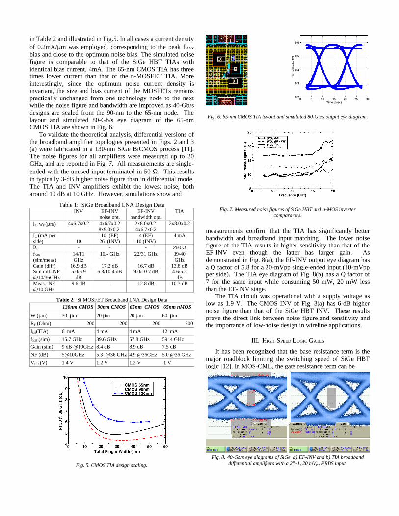
bias and close to the optimum noise bias. The simulated noisefigure is comparable to that of the SiGe HBT TIAs withidentical bias current, 4mA. The 65-nm CMOS TIA has threetimes lower current than that of the n-MOSFET TIA. Moreinterestingly, since the optimum noise current density isinvariant, the size and bias current of the MOSFETs remainspractically unchanged from one technology node to the nextwhile the noise figure and bandwidth are improved as 40-Gb/sdesigns are scaled from the 90-nm to the 65-nm node. Thelayout and simulated 80-Gb/s eye diagram of the 65-nmCMOS TIA are shown in Fig. 6.
To validate the theoretical analysis, differential versions ofthe broadband amplifier topologies presented in Figs. 2 and 3(a) were fabricated in a 130-nm SiGe BiCMOS process [11].The noise figures for all amplifiers were measured up to 20GHz, and are reported in Fig. 7. All measurements are single-ended with the unused input terminated in 50 Ω. This resultsin typically 3-dB higher noise figure than in differential mode.The TIA and INV amplifiers exhibit the lowest noise, botharound 10 dB at 10 GHz. However, simulations show and
Table 1: SiGe Broadband LNA Design DataINV EF-INV
noise opt.EF-INV
bandwidth opt.TIA
lE, wE (µm) 4x6.7x0.2 4x6.7x0.28x9.0x0.2
2x8.0x0.2 4x6.7x0.2
2x8.0x0.2
IC (mA perside) 10
10 (EF)26 (INV)
4 (EF)10 (INV)
4 mA
RF - - - 260 Ωf3dB
(sim/meas)14/11GHz
16/- GHz 22/31 GHz 39/40GHz
Gain (diff) 16.9 dB 17.2 dB 16.7 dB 13.8 dBSim diff. NF@10/36GHz
5.0/6.9dB
6.3/10.4 dB 9.0/10.7 dB 4.6/5.5dB
Meas. NF@10 GHz
9.6 dB - 12.8 dB 10.3 dB
Table 2: Si MOSFET Broadband LNA Design Data130nm CMOS 90nm CMOS 65nm CMOS 65nm nMOS
W (µm) 30 µm 20 µm 20 µm 60 µm
RF (Ohm) 200 200 200 200
IDS(TIA) 6 mA 4 mA 4 mA 12 mA
f3dB (sim) 15.7 GHz 39.6 GHz 57.8 GHz 59. 4 GHz
Gain (sim) 9 dB @10GHz 8.4 dB 8.9 dB 7.5 dB
NF (dB) 5@10GHz 5.3 @36 GHz 4.9 @36GHz 5.0 @36 GHz
VDD (V) 1.4 V 1.2 V 1.2 V 1 V
measurements confirm that the TIA has significantly betterbandwidth and broadband input matching. The lower noisefigure of the TIA results in higher sensitivity than that of theEF-INV even though the latter has larger gain. Asdemonstrated in Fig. 8(a), the EF-INV output eye diagram hasa Q factor of 5.8 for a 20-mVpp single-ended input (10-mVppper side). The TIA eye diagram of Fig. 8(b) has a Q factor of7 for the same input while consuming 50 mW, 20 mW lessthan the EF-INV stage.
The TIA circuit was operational with a supply voltage aslow as 1.9 V. The CMOS INV of Fig. 3(a) has 6-dB highernoise figure than that of the SiGe HBT INV. These resultsprove the direct link between noise figure and sensitivity andthe importance of low-noise design in wireline applications.
III. HIGH-SPEED LOGIC GATES
It has been recognized that the base resistance term is themajor roadblock limiting the switching speed of SiGe HBTlogic [12]. In MOS-CML, the gate resistance term can be
Fig. 6. 65-nm CMOS TIA layout and simulated 80-Gb/s output eye diagram.
0 5 10 15 20 25 300.2
0.3
0.4
0.5
0.6
Time (psec)
Am
pli
tud
e (
V)
Fig. 7. Measured noise figures of SiGe HBT and n-MOS invertercomparators.
Fig. 5. CMOS TIA design scaling.
Fig. 8. 40-Gb/s eye diagrams of SiGe a) EF-INV and b) TIA broadbanddifferential amplifiers with a 231-1, 20 mVp-p PRBS input.
rendered negligible through layout techniques by reducing theunit finger width. We have recently proposed a novelBiCMOS-ECL logic family that employs a cascode stageconsisting of a MOSFET common-source device followed bya common-base HBT [13]. Such a structure takes advantage ofthe large intrinsic slew rate of the HBT and of the small gateresistance of the MOSFET, resulting in faster switching speedthan either MOS or HBT CML families. At the same time, as aresult of the low MOSFET threshold voltage and superior fT atlow VDS, it operates with lower (less than 2.5 V) supplyvoltages than SiGe HBT ECL.
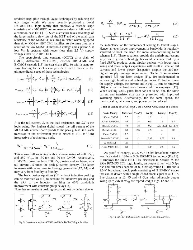
The open-circuit time constant (OCTC) of a chain ofCMOS, differential MOS-CML, cascode HBT-CML andBiCMOS cascode [13] inverter chain (Fig. 9) with a stage-to-stage loading factor of k can provide a useful metric of theultimate digital speed of these technologies.
CMOS 3 r o
2
C gd C db k R g
r o C gs 1 gm r o C gd (9)
MOSCML
VI T Cgd Cdb k Rg
RL Cgs 1 gm RL Cgd (10)
HBTCML V
I T C Ccs k Rb
RL C 1 gmRL C ! (11)
"BiCMOSCML #$ V
I T % C '& Ccs &)( k & Rg
RL *,+ Cgs & Cgd -/. (12)
IT is the tail current, RL is the load resistance, and ∆V is thelogic swing. For highest digital speed, the tail current of theMOS-CML inverter corresponds to the peak fT bias (i.e. eachtransistor in the differential pair is biased at 0.15 mA/µm)irrespective of technology node.
W 0 I T
0.3mA 132 m; AE 0 I T
1.5J peakfT
(13)
This allows full switching with a voltage swing of 450 mVp-p
and 350 mVp-p in 130-nm and 90-nm CMOS, respectively.HBT-CML inverters have 250 mVp-p swing and are biased at atail current 1.5 times the peak fT current density. The latterincreases with every new technology generation [12, 14] andmay vary from foundry to foundry.
The basic design equations (14) without inductive peakingcan be modified as (15) to account for inductive peaking andthe SRF of the inductor, resulting in 60% bandwidthimprovement with constant group delay (14).Note that series-shunt peaking occurs almost by default due to
R L 0 $ VI T
; BW 3dB 0 12 4 R L C L
0 I T
2 4 C L $ V (14)
Lp 0 C L R L2
3.10 C L
3.1 $ V 2
I T2
; I Tmin 0 $ V 5 C L
3.1Lpmax
(15)
the inductance of the interconnect leading to fanout stages.Hence, an even larger improvement in bandwidth is regularlyachieved without the need for more area-consuming t-coilschemes [15]. These equations provide the underlying reasonswhy, for a given technology back-end, characterized by afixed SRF*L product, using bipolar devices with lower logicswing and lower output capacitance will result in smaller tailcurrents and lower power dissipation despite the 200-mVhigher supply voltage requirement. Table 3 summarizesoptimized full rate latch designs (Fig. 10) implemented invarious logic families and technology nodes. To further lowerthe supply voltage, the current tail in Fig. 10 can be removed[16] or a narrow band transformer could be employed [17].When scaling CML gates from 90 nm to 65 nm, the samecurrent and transistor size can be preserved with improvedswitching speed. Alternatively, for the same speed, thetransistor size, tail current, and power can be reduced.
Table 3: Scaling of CMOS, MOS-, and BiCMOS-CML fanout-of-1 latches
Latch Family Rate:Gbs VDD (V) ∆V (V) IT (mA) PD(mW)
130-nm CMOS 5.5 1.2 1.2 -
130-nm MOSCML 40 1.8 0.5 1.5 2.7
BiCMOS CML 40 1.8 0.2 0.83 (1.5) 1.5 (2.7)
BiCMOS ECL 50 2.5 0.25 4 10
90-nm CMOS 7.5 1 1 -
90-nm MOSCML 40 1.2 0.38 2.75 3.3
65-nm CMOS 11.5 1 1 -
65-nm MOSCML 60 1 0.35 2.5 2.5
As proof of concept, a 2.5-V, 45-Gb/s broadband retimerwas fabricated in 130-nm SiGe BiCMOS technology (Fig.11).It employs the SiGe HBT TIA discussed in Section II, theSiGe BiCMOS ECL logic family, an output driver with 5.5psrise and fall times capable of 80 Gb/s operation [1, 10] and a2.5-V broadband clock path consisting of 3 EF-INV stagesthat can be driven with a single-ended clock signal at 49 GHz.Eye diagrams at 10, 45 and 49 Gb/s with adjustable outputswing up to 2x600 mVpp are reproduced in Figs. 12 and 13.
Fig. 9. Inverters in various CMOS and SiGe BiCMOS logic families.
Wn
Wp
kWn
kWp
∆V
∆V
IT
RL
∆V
∆V
RL
IT
IT
INN IN
P
OUTP OUTN
RL
RL
Fig. 10. 40-Gb/s 130-nm MOS- and BiCMOS-CML Latches.
250 Ω
VDD
= 1.8 V
1 nH
0.825 mA
Q1
Q2
Q3 Q
4
1 nH
250 Ω
CLK
DATA
OUT
330 Ω
VDD
= 1.8 V
1 nH
1.5 mA
Q1
Q2
Q3 Q
4
1 nH
330 Ω
CLK
DATA
OUT
CLK
DATA
OUT
IV. MM-WAVE OSCILLATOR TOPOLOGIES
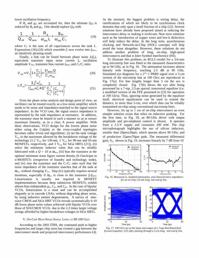
The cross-coupled VCO topologies of Fig. 14 have beenvery popular [18,19] in (SOI) CMOS technology due to thelow bias current required to achieve negative resistance andoscillation at frequencies as high as 60 GHz in 90-nm SOI[18]. However, at mm-wave frequencies, even CMOSdesigners [20] have recognized the benefits of the Colpittstopology. The latter has been favoured in bipolarimplementations [21] as a result of its lower parasiticcapacitance and built-in buffering of the resonant tank fromthe load.
For each of the three topologies above, one can derive theexpressions for the maximum oscillation frequencies and finda direct link to the fundamental device characteristics of agiven semiconductor technology.
osc n MOS g ' m Q eff
C ' gs 4C ' gd
C ' db C L
W
(16)
osc CMOS 23
g ' m Q eff
C ' gs 4C ' gd
C ' db C L
W
(17)
osc + Colpitts - g ' m Q eff
C ' gs & C ' sb
(18)
Qeff is the effective quality factor of the L-C-varactor tankwhich includes the loading effect of the transistor. CL is theload capacitance and g'm, C'gs, C'gd, C'sb, C'db, represent thetransconductance and parasitic capacitances of the transistorper unit gate width. Since only g'm improves with scalingwhile the rest remain largely unchanged over nodes andfoundries, ωosc will also scale if the MOSFET gate width andcurrent remain constant. C'
sb has no equivalent in HBTs andboth C'sb and C'db are small in SOI, thus explaining why recordωosc are obtained with HBT and SOI processes. It isinteresting to note that: (i) the load capacitance places anupper bound on ωosc of cross-coupled topologies, but does notaffect the Colpitts topology, (ii) if CL is ignored, the transistorparasitic capacitances, tank Q, and g'm ultimately limit ωosc ,(iii) the maximum possible oscillation frequency does notdepend on the tail current ISS nor does it depend on thetransistor size as long as a small enough inductor L withadequate Q can be realized and the load is negligible, and (iv)for the same Q, and CL=0, the n-MOS cross-coupled and theColpitts VCOs have almost the same maximum oscillationfrequency while the CMOS cross-coupled VCO has 2/3 times
Fig. 11. Broadband 49 Gb/s 2.5-V retimer layout
Fig. 13. a) 45 Gb/s, and b) 49 Gb/s 2x600mVpp retimed output
Fig. 12. a) 10 Gb/s and b) 45 Gb/s input (top) and 2x280mVpp output(bottom) after retiming
Fig. 14. Cross-coupled MOS VCO topologies
Fig. 15. a) 70-GHz 65-nm CMOS and b) 35-GHz 130-nm BiCMOS ColpittsVCO schematics
!
µ " # $ % " !µ " # $ % " & (' ' ) (* + & (' ' ) (* +& ,* + & ,* +
- /. 0
! /. 0) /. 0) /. 0
1 !
- /. 0
- /. 0 1 ' $/. +
! /. 0
!µ " ! % " !
µ " ! % " - ,* + - ,* + ,* + ,* +& ! $2. 0
- /. 0
! /. 0! /. 0 1 - ' $
& ! $2. 0 1 !,. +
- /. 0 3
µ " 3µ "
4 5
lower oscillation frequency.If Rg and gds are accounted for, then the ultimate Qeff is
reduced by Rg and gds. One should replace Qeff with
1Q eff
1Q tank
R gosc L
g dsosc C T
(19)
where CT is the sum of all capacitances across the tank L.Expressions (16)-(18) which resemble fT now evolve into fMAX.,an intuitively pleasing result.
Finally, a link can be found between phase noise L(fm),equivalent transistor input noise current In, oscillationamplitude VOSC, transistor bias current IBIAS, and C1/C2 ratio.
V osc V 1
1 C 1
C 2 2 I BIAS Q
C 2 osc
(20)
L f m I n 2 osc
2
I BIAS2 m
2 4Q 2
1C 1
2
C 22
1C 1
C 2
1 2 (21)
From the phase noise analysis and design point of view, anoscillator can be treated exactly as a low-noise amplifier whichneeds to be noise and impedance-matched to the signal sourceimpedance. In the VCO case, the signal source impedance isrepresented by the tank impedance at resonance. In addition,the transistor must be biased in such a manner so as to ensuremaximum linearity, as in a class A power amplifier. Withthese observations, VCO design for the lowest phase noiseeither using the Colpitts or the cross-coupled topologiesbecomes rather trivial and algorithmic: (i) set the tank voltageVosc to the maximum allowed by the breakdown voltage of thetechnology (1.2 Vp-p for 130-nm, 1 Vp-p for 90-nm and 65-nmMOSFETs, respectively, and 3 Vp-p for SiGe HBTs [21]), (ii)select the minimum inductor value that can be reliablyfabricated with a Q > 10 at ωosc, (iii) bias the transistor at theoptimal minimum noise figure current density (0.15mA/µm inn-MOSFETs irrespective of foundry and technology node),and (iv) size the transistor and the C1/C2 ratio such that thenoise impedance of the transistor matches that of the tank atωosc, without changing Vosc. Step (iv) typically requires severaliterations, especially if ωosc is close to the transistor fT/fMAX.Linearization is usually not required in MOSFETimplementations because deep submicron MOSFETs exhibitalmost bias-independent gm, Cgs, and Cgd. In the case of bipolarVCOs, linearization is a must and can be accomplishedelegantly as in cascode LNAs, without degrading phase noise,by using inductive emitter degeneration. A survey of mm-wave CMOS and SiGe HBT VCOs reveals systematically 6-10dB lower phase noise values achieved with bipolar VCOs overthose of SOI/CMOS VCOs due to the 2-3 times larger voltageswings afforded by higher breakdown voltages in SiGe HBTs.
V. ON-CHIP HIGH-SPEED SERIAL L INKS AT 80-100 GB/S
According to the 2003 ITRS, the continued push to higherfrequenciesand larger chip sizes hascreated a gap between theinterconnect needs and projected interconnect performance [4].
At the moment, the biggest problem is wiring delay, theramifications of which are likely to be synchronous clockdomains that only span a small fraction of a chip [22]. Severalsolutions have already been proposed aimed at reducing theinterconnect delay or making it irrelevant. Near term solutionssuch as the introduction of copper wires and low-k dielectricswill help reduce the delay. In the long term, asynchronousclocking and Network-on-Chip (NOC) concepts will helpavoid the issue altogether. However, these solutions do notaddress another problem of long, on-chip, high-speedinterconnects and that is Inter Symbol Interference (ISI).
To illustrate this problem, an RGLC-model for a 3.6-mmlong microstrip line was fitted to the measured characteristicsup to 94 GHz, as in Fig. 16. The attenuation increases almostlinearly with frequency, reaching 2.5 dB at 90 GHz.Simulated eye diagrams for a 210 1− PRBS signal over a 5-cmversion of the microstrip line at 100 Gb/s are reproduced inFig. 17(a). For line lengths longer than 3 cm the eye iscompletely closed. Fig. 17(b) shows the eye after beingprocessed by a 7-tap, 2.5-ps spaced, transversal equalizer (i.e.a modified version of the FFE presented in [23] for operationat 100 Gb/s). Thus, ignoring noise generated by the equalizeritself, electrical equalization can be used to extend thedistance, to more than 5-cm, over which data can be reliablytransmitted on-chip using conventional microstrip lines.
However, for up to 1 cm of on-chip interconnect an evensimpler solution exists that relies on inductive peaking. Forthe first time, in Fig. 18, an 80-GHz driver with outputamplitude and pre-emphasis control is shown. It operatesfrom a 2.5-V supply and consumes 200 mW. The chipmicrophotograph highlights the use of silicon inductors,smaller than 20µmx20µm, which operate above 90 GHz, andof production 55µmx70µm pads. The measured differentialgain, S21, shown in Fig. 19, increases linearly by 7 dB from 10
Fig. 16. Measured vs. modeled attenuation and characteristics impedancefor an on-chip 3.6-mm long microstrip line.
0 20 40 60 80 100−2.5
−2
−1.5
−1
−0.5
0
Frequency (GHz)
|S21
| (dB
)
MeasuredModelled
0 20 40 60 80 10045
50
55
60
65
Frequency (GHz)
ZC
(Ω
)MeasuredModelled
Fig. 17. 100 Gb/s eye at the input and output of a 7-tap distributed feedforward equalizer [23] after passing through a 5-cm long microstrip line.
0 10 20−40
−30
−20
−10
0
10
20
30
40
Time (ps)
Am
plit
ud
e (
mV
)
0 10 20−60
−40
−20
0
20
40
60
Time (ps)
Am
plit
ud
e (
mV
)

GHz to 65 GHz, peaking above 10 dB in the 65-GHz to 75-GHz range. More than 10 dB of gain control is achieved overthe entire frequency range. The output return loss, better than-10 dB up to 94 GHz, is also shown in Fig. 19 and remainsunchanged as a function of the pre-emphasis control current.
VI. CONCLUSIONS
Algorithmic design methodologies have been developed forthe main circuit building blocks that make up a wirelinetransceiver. The theory was experimentally verified on 40-Gb/s SiGe BiCMOS preamplifiers, a 49-Gb/s retimer and onan 80-GHz output driver with pre-emphasis, all fabricated in130-nm SiGe BiCMOS technology and operating from 2.5-Vsupply. The prospects of 90-nm and 65-nm CMOS technologyfor low-voltage/low-power 40-Gb/s and 80-Gb/s transceivershave also been investigated and proof-of-concept buildingblocks are currently in fabrication. More importantly, CMOSlow-noise preamplifier and CML gate designs have beenshown to scale almost unchanged in terms of transistor sizeand current from 90-nm to 65-nm node while their noise andbandwidth are improved.
ACKNOWLEDGEMENTS
The authors thank NSERC, Micronet, STMicroelectronics, andGennum for financial support and STMicroelectronics Crolles forchip fabrication. An equipment grant from CFI and OIT, and CADtools from CMC are also acknowledged. Special thanks go toBernard Sautreuil of STMicroelectronics for help in this project.
REFERENCES
[1] T. Dickson et al., “A 72Gb/s 231-1 PRBS Generator in SiGe BiCMOSTechnology,” ISSCC Digest, pp.342-343, Feb. 2005.
[2] S.P. Voinigescu, et al., “A comparison of Si CMOS, SiGe BiCMOS, andInP HBT technologies for high-speed and millimeter-wave ICs,” SiRF-2004, pp. 111-114, Sept. 2004.
[3] S.P. Voinigescu, “RF and High-Speed Integrated Circuits,” ECE1364S,lecture notes and midterm exam, University of Toronto, 2005.
[4] “ International Technology Roadmap for Semiconductors 2003 Edition
interconnect,” ITRS, 2003/2004.[5] G.D. Vendelin, et al., Microwave Circuit Design Using Linear and
Nonlinear Techniques, Toronto, John Wiley & Sons, 1990.[6] S.P. Voinigescu et al, “A scalable high-frequency noise model for bipolar
transistors with application to optimal transistor sizing for low-noiseamplifier design,” IEEE J. Solid-State Circuits, vol. 32, no. 9, Sept. 1997.
[7] A.N. Karanicolas, “A 2.7-V 900-MHz CMOS LNA and Mixer,” IEEEJ. Solid-State Circuits, vol. 31, no. 12, , pp.1939-1944, Dec. 1996.
[8] C. Kromer, et al. “A 100mW 4x10Gb/s Transceiver in 80nm CMOS forHigh-density Optical interconnects,” ISSCC Digest, pp.334-335, 2005.
[9] H. Tran et al, “6-kΩ, 43-Gb/s differential transimpedance-limitingamplifier with auto-zero feedback and high dynamic range,” IEEE GaAsIC Symp. Tech. Dig., pp. 241-244, Nov. 2003.
[10] M.. Meghelli, “A 108Gb/s 4:1 Multiplexer in 0.13 µm SiGe-BipolarTechnology,” ISSCC Digest, pp.236-237, Feb. 2004.
[11] M. Laurens et al, “A 150 GHz fT/fMAX 0.13 µm SiGe:C BiCMOStechnology,”Proc. IEEE BCTM, Sept. 2003.
[12] G. Freeman et al. “Transistor Design and Application Considerations for>200 GHz SiGe HBTs,” IEEE Trans ED, Vol.50, No.3, pp.645-655,2003.
[13] T.O. Dickson et al., “A 2.5-V, 40-Gb/s Decision Circuit Using SiGeBiCMOS Logic,” Dig. Symp. VLSI Circuits, pp. 206-209, June 2004.
[14] M. Rodwell, et al., “ Transistor and Circuit Design for 100-200 GHzICs,” IEEE CSICS Technical Digest, pp.207-210, Oct. 2004.
[15] J. Kim, et al., "Circuit Techniques for a 40Gb/s Transmitter in 0.13µmCMOS," ISSCC Digest, pp.150-151, Feb. 2005.
[16] K. Kanda, et al., “40Gb/s 4:1 MUX/1:4 DEMUX in 90nm StandardCMOS,” ISSCC Digest, pp.152-153, Feb. 2005.
[17] D. Kehrer et al., “A 60Gb/s 2:1 Selector in 90nm CMOS,” IEEE CSICSDigest, pp.105-108, Oct. 2004.
[18] F. Ellinger, et al., “60 GHz VCO with Wideband Tuning RangeFabricated on VLSI SOI CMOS Technology,” IEEE MTT-S Digest,pp.1329-1332, June 2004.
[19] J. Kim, et al., “A 44GHz Differentially Tuned VCO with 4GHz TuningRange in 0.12µm SOI CMOS Technology,” ISSCC Digest, pp.416-417,Feb. 2005.
[20] P.-C. Huang, et al., “A 114GHz VCO in 0.13µm CMOS Technology,”ISSCC Digest, pp.404-405, Feb. 2005.
[21] C. Lee, et al., “SiGe BiCMOS 65-GHz BPSK Transmitter and 30 to 122GHz LC-Varactor VCOs with up to 21% Tuning Range,” IEEE CSICS,Technical Digest, pp.179-182, Oct. 2004.
[22] S. Kumar, et al., “A network on chip architecture and designmethodology,” in IEEE Computer Society Annual Symposium on VLSI,pp. 105–112, April 2002.
[23] A. Hazneci and S. P. Voinigescu, "49-Gb/s, 7-Tap Transversal Filter in0.18µm SiGe BiCMOS for Backplane Equalization," IEEE CSICS,Technical Digest, pp.101-104, Oct.2004 .
Fig. 18. 80-GHz Driver with peaking control for pre-emphasis at 80 Gb/s.
µ
Ω
µ
Ω
µ µ
!
!
! !
! !
!
µ
Ω
µ
Fig. 19. Measured S parameters for 80-GHz driver as a function ofpre-emphasis control.
Related Documents