Steve Anderson, Senior Director Product and Technology Marketing, STATS ChipPAC Advanced Packaging For Mobile and Growth Products 7-Dec-2011 © STATSChipPAC 2011

Welcome message from author
This document is posted to help you gain knowledge. Please leave a comment to let me know what you think about it! Share it to your friends and learn new things together.
Transcript

Steve Anderson, Senior Director
Product and Technology Marketing, STATS ChipPAC
Advanced Packaging For Mobile and Growth Products
7-Dec-2011 © STATSChipPAC 2011

2 2
Growing Needs for Silicon & Package Integration
New converged applications require more complex & customized packaging solutions
Computing
Communication
US$125.4B - 2010 US$136.1B – 2013
2.8% CAGR
US$70.3B - 2010 US$80.9B – 2013
4.8% CAGR
Converged Market Mobile Computing
Convergent Products US$28.8B
37.5% CAGR
Packaging Trend
3D SIP PoP/PiP, FBGA-SD,
ISM, Module
3D IC F/BGA-TSV-SD, PoP-
TSV, eWLB, IPD
2D SoC QFN, FBGA, fcBGA,
fcFBGA, eWLB, WLCSP
Implication to OSAT
• Capital intensive • Silicon interface know-how • 2.5D IC using Si interposer • Yield & cycle time
• Die thinning & stacking
• Advanced multi-tiers wire bonding
• Passives discrete handling or IPD
• Yield & cycle time
• Pressure on packaging cost • Needs for best valued BOM • More flip chip & WLP (capital
intensive) • Yield & cycle time
7-Dec-2011 © STATSChipPAC 2011

3 3
Heterogeneous integration; advanced 3D PKG solutions
Micro Electronics
MEMS
RF
Photonics
Sensors
Consumer Electronics Energy Automotive Healthcare Computing &
Communications
Design Nano-Materials & Components System Interconnections Thermal
§ CMOS IC to 22nm & Beyond § IC & 3D Module & 3D IC Pkg: eWLB/
Fanout Wafer Level PKG
§ 3D IC Systems with TSV
Die Area Reduction
7-Dec-2011 © STATSChipPAC 2011

4 4
Drivers for Mobile /Portable Device Packaging
• Size (area and thickness) • Performance • Cost • Standardized • Reliability • Environmental
7-Dec-2011 © STATSChipPAC 2011

5 5
WLCSP (wafer level CSP) • Many Billions of Packages Shipped • Established worldwide Industry Infrastructure • Lead free & MSL1 • I/O ranging 12 – 144
Smart Phone WLCSP Statistics • Apple iPhone 48 dies - 21% are WLCSP • RIM Blackberry Storm 42 dies - 29% are WLCSP • Nokia 95 50 dies - 50% are WLCSP
More and More WLCSPs in mobile phones
7-Dec-2011 © STATSChipPAC 2011

6 6
Advanced Wafer Level Integration Technology Evolution
EMBEDDED & 3D PACKAGING
3D TSV ICs
TSV Interposer
LEADED PACKAGING
ARRAY PACKAGING
eWLB • Advanced node compatibility • Large Scale • Low cost
• Higher integration • Performance • Reliability • Design Flexibility
7-Dec-2011 © STATSChipPAC 2011
7 7
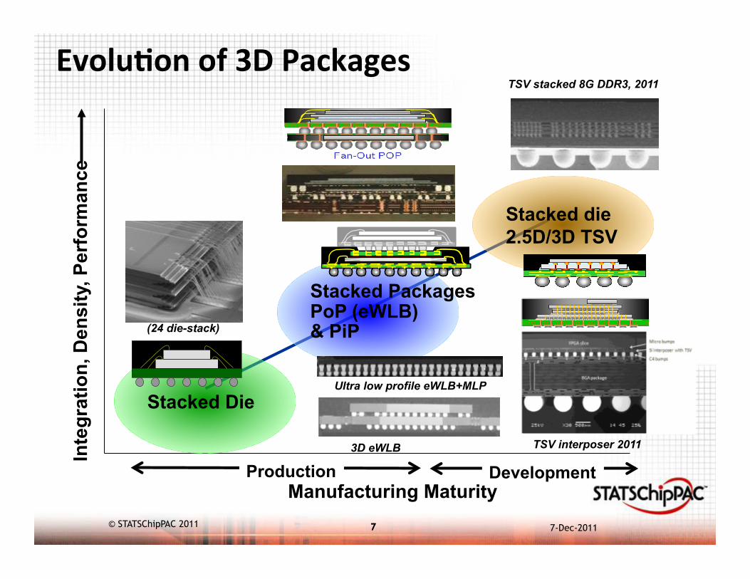
Evolu&on of 3D Packages
7
Inte
grat
ion,
Den
sity
, Per
form
ance
Manufacturing Maturity
Stacked die 2.5D/3D TSV
Stacked Die
Stacked Packages PoP (eWLB) & PiP
Production
TSV stacked 8G DDR3, 2011
(24 die-stack)
3D eWLB TSV interposer 2011
Development
Ultra low profile eWLB+MLP
7-Dec-2011 © STATSChipPAC 2011

8 8
Portable/Mobile Electronics- Package Trends - Stacked Die Packages
- Package on Package (PoP)
- eWLB / FO-WLP / EDS
- Through Silicon Vias (TSV)
3D Chip Packaging Solutions • SiP–System in package • SoP–System on package (High Density Heterogeneous / Modular Chips Integration) • SoC–System on chip (Single Chip- Chip Level Integration) • Chip packaging compatibility with SMT assembly process • 3S Reliability • 3S Assembly process, material and rework
7-Dec-2011 © STATSChipPAC 2011

9 9
Silicon Interposer Delivers High Interconnect Density
7-Dec-2011 © STATSChipPAC 2011

10 10
eWLB and Wafer Level Packaging Technology
7-Dec-2011 © STATSChipPAC 2011

11 11
Driving Forces to Wafer Level Package
Wafer Level
Packages
§ Packaging cost § Test cost
Cost • Batch processing • High parallelism • Improved test concepts
Dimensions
• Smallest package heights • Minimum lateral area
§ Interconnect line length (ò) § Operating frequencies (ñ) § Package Speed (ñ) § Parasitics
Electrical Performance
• Min line length • Multilayer RDL • Reduced no. of • interconnects
§ Power consumption (ñ) § Package Density (ñ)
Thermal Performance
§ Integrated Passives (R, L, C) § System in Package § 3D
Functionality (Integration)
• Integrated passives in RDL • SiP/ 3D capability
§ Pitches (ò) § No standards § Small chips/ high no. of I/Os
I/O Density • Min pitches
§ Package height (ò) § Lateral dimensions (ò)
• Improved chip to board coupling
7-Dec-2011 © STATSChipPAC 2011

12 12
What is eWLB ? • A new Wafer Level Packaging technology, utilizes well developed wafer
bumping infrastructure, with an innovative wafer reconstitution process to package Known Good Dice.
• Wafer level package, uses mold compound to support the fan-out I/Os.
• Fan-In Interconnects only - Number and pitch of Interconnects must be adapted to the chip size
• Only Single chip packaging solution
• Fan-out Interconnects - #, Pitch of Interconnect is INDEPENDENT of chip size
• Single/Multi/3D chip packaging solution
• Improved Yield with KGD
Fan-In WLP eWLB/Fan-Out WLP PKG size = Chip size PKG size > Chip size
eWLB expands the application space for Wafer Level Packaging!
chip chip
7-Dec-2011 © STATSChipPAC 2011

13 13
Advantages of eWLB Technology
• Thinner & smaller package solution
– Ideal for mobile applications and meeting future roadmaps
• Package robustness (vs. LF flip chip + advanced fab nodes with ELK)
– Cu/ELK compatible packaging technology (65nm in HVM, 40nm in Qualification)
– Green packaging (Generic Pb-free, Halogen free)
• Superior board level reliability proven for mobile applications
• Proven lower cost path using a batch process & simpler supply chain
• Next generation eWLB technology with 3D eWLB joint development
• No substrate or bumping; Simple logistics and supply chain
Solder ball
Cu-RDL
Si Chip
EMC
7-Dec-2011 © STATSChipPAC 2011

14 14
eWLB Products Portfolio
eWLB-‐MLP
2.5D / Extended eWLB
2D eWLL
7-Dec-2011 © STATSChipPAC 2011

15 15
Thin packaging solution (<0.5mm)
Embedded Passives
Multi-die eWLB
Plated Cu RDL 10mm
for more design and routing flexibility
10mm/10mm line width and line spacing
3D (double-side) eWLB
250mm thin eWLB
Next Generation eWLB
7-Dec-2011 © STATSChipPAC 2011

16 16
Multi-Die eWLB (Side-by-side) 2-die eWLB • PKG: 12x12sqmm, 0.4mm ball pitch • Die: 4x4mm (2 dies) • I/O Count: 580 • 2-L RDL
3-die eWLB • PKG: 12x12sqmm, 0.5mm ball pitch • Die : 3-die, 2 (3x3mm) + 3x4mm) • I/O Count: 396 • 1-L RDL
Reliability Test Pre-condition Test Condition Read-out Pass
Multiple Reflow - LF bumps @ 260oC 5x, 10x, 20x √ passed
Unbiased HAST MSL1 130oC, 85%RH 96hr √ passed
Temperature Cycling MSL1 -55oC/125oC (G) 500x, 850x √ passed
High Temp. Storage MSL1 150oC 500, 1000hr √ passed
TCoB -40/125C 500x √ passed
Drop test Nokia Spec - √ passed
Highly integrated SiP or side-by-side packaging solution with multi-die. Can be integrated with IPD, RDL passives or discrete MLCCs.
2-die eWLB • PKG: 8x8 sqmm, 0.5mm ball pitch • Die : 2-die, 2 (5x2.5 mm) • I/O Count: 192 • 1-L RDL
7-Dec-2011 © STATSChipPAC 2011

17 17
Double-side 3D eWLB Package Specification • PKG: 12x12sqmm, 0.5mm ball pitch • Die : 3-die, 2 (3x3mm) + 3x4mm) • I/O Count: 396 • 1-L RDL (Top and Bottom both) • Thickness 450um / 250um
450um 250um
Low profile 3D eWLB PoP (12x12mm PoP-bottom package) with less than 1mm thickness including solder balls.
1.2mm
<1.0mm
250um Thin Bottom 3D PKG
Picture of 3D eWLB PoP packages; Total less than 1.0 mm package height (including solder balls)
Passed JEDEC component level and board level reliability tests
7-Dec-2011 © STATSChipPAC 2011

18 18
Ultra Low Profile eWLB PoP: eWLB-MLP (embedded Wafer level Molded Laser PoP)
– Thin POP (250um pkg body thickness)
– Low warpage during solder reflow cycles
– Larger Si die cavity
– Flexibility in memory interface
– High routing density: L/S=10/10 (um)
– Compatible with ELK
– Good thermal performance
§ QJA 18~22(oC/W)
§ QJB 3~7(oC/W) for 12x12mm eWMLP)
Si RDL
MLP eWLB
eWLB-MLP
+Memory
7-Dec-2011 © STATSChipPAC 2011

19 19
eWLB : Themo-Moire, High Temperature Warpage Measurement
fcVFBGA,7x7mm, 191LD NSP
PKG height 0.95 mm Die 4.46 x 5.65 x 0.19 mm
eWLB 8x8mm, 182I/O
PKG height 0.7 mm Die 5 x 5 x 0.45 mm
7-Dec-2011 © STATSChipPAC 2011
20 20
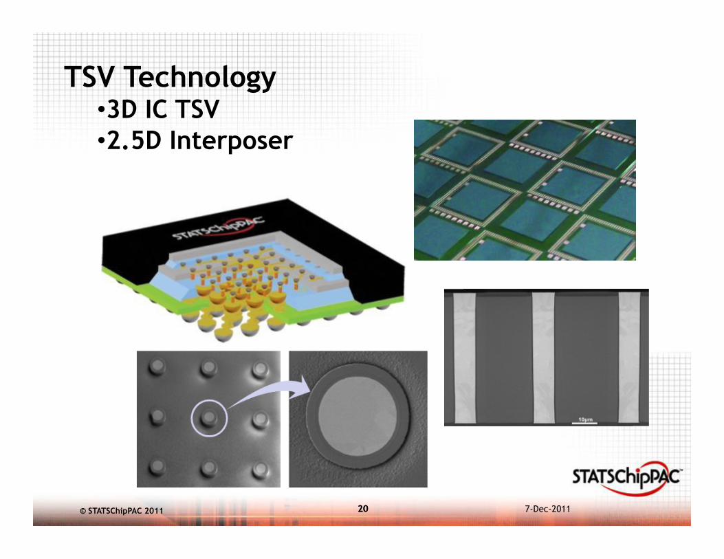
TSV Technology • 3D IC TSV • 2.5D Interposer
7-Dec-2011 © STATSChipPAC 2011

21 21
TSV Technology for mobile devices (Logic + Memory) – Wide I/O memory interface in mobile - Examples: AP+DRAM or AP/BB combo+DRAM in mobile devices
• High Performance Devices – High electrical performance solution : Increasing number of I/Os
– Power effective solution : Minimized output loading with CtC connection
– TSV for shorter interconnection length for better performance
– Micro-bump
– Micro-bump bonding (50/40um pitch): Thermal Compression with NCP
– Thin wafer handling and packaging TSV
7-Dec-2011 © STATSChipPAC 2011

22 22
Lower cost (High yield) & higher performance For embedded memory; • Nominal LSI Memory capacity↑ 2X per node • eDRAM shrinks < 40% per node • Total memory area grows node to node
• De-couple functional blocks in SoC (analogue, memory, I/O, RF,…) • Heterogeneous integration in Pkg
TSV Technology for high performance processors: Examples: GPU + DRAM, MPU + DRAM, Logic + Analog, sliced FPGA integration
2D - SoC
2.5D – TSV interposer
3D – TSV in Device
eDRAM capacity (Mb) needs
1 3 0 n m 9 0 n m 6 5 n m 4 5 n m
7-Dec-2011 © STATSChipPAC 2011

23 23
No void observed after TCB with NCP)
40/50um pad pitch with ENIG pad finish on Cu pad
Chip-to-Substrate
Chip-to-Chip
40um pitch Cu column on Substrate
Thermo-compression Bonding – Thermo-compression Bonding (TCB) of 40um pitch with Cu column and NCP (non-conductive paste)
7-Dec-2011 © STATSChipPAC 2011

24 24
TSV Silicon Interposer (TSI) Technology Provide High Complexity, High Performance ASICs with
Dependable Predictability
Technology Disaggregation
• Optimization of Silicon Technology for Individual IP
• Higher Levels of System Integration
• Wider Product Capability Offering to Customers
• Lower Total System Power
7-Dec-2011 © STATSChipPAC 2011

25 25
External Memory Solutions • Increase Memory Options for Customers • Increase Memory Storage per ASIC • Low Power and Higher Bandwidth • Leverage Industry Standard Memories Die Separation • Decrease Yield Losses of Large Die • Decrease Yield Losses Early in
TSV Silicon Interposer (TSI) Technology -‐ Con&nued
7-Dec-2011 © STATSChipPAC 2011

26 26
Func&onal Par&&oning with TSI Heterogeneous Integration • Silicon interposer advantages – Reduced die complexity – Mixed technologies
Source: Xilinx 2.5D FPGA
7-Dec-2011 © STATSChipPAC 2011

27 27
• 3D especially with TSVs is a revolutionary change requiring significant infrastructure additions.
• 2.5D allows use of mixed interconnect ICs from different sources and is evolutionary.
• 2.5D may become as essential within a package assembly as underfill epoxy for both single chips and stacked 3D chips.
• 2.5D is not limited to silicon – glass and even organic solutions provide economical benefits in applications where silicon is inappropriate.
2.5D and 3D will Coexist ?
7-Dec-2011 © STATSChipPAC 2011

28 28
Summary • Wafer level packaging is a key technology enabler for future
heterogeneous integration.
• Next generation and 3D eWLBs would be a good solution for future needs in mobile/portable applications, such as PoP and 3D SiP.
• With scale-up and higher throughput, large panel approach is next step for further market-penentration as cost-effective packaging solutions.
• TSV technology is critical for continued evolution of semiconductor industry. TSV interposer technology is one of early application of TSV technology.
• As with all new technologies for 2.5D/3D TSV wafer level integration; Product applications & drivers are critical.
• Alternative technology, eWLB technology, wafer level packaging solution enabling 3D wafer level integration with low cost solution.
• More collaborative cost/ performance analysis across FE-BE FAB, EDA, Assembly, Reliability, Metrology & Test are needed for successful TSV biz establishment.
7-Dec-2011 © STATSChipPAC 2011

29 29
Thank You
7-Dec-2011 © STATSChipPAC 2011
Related Documents