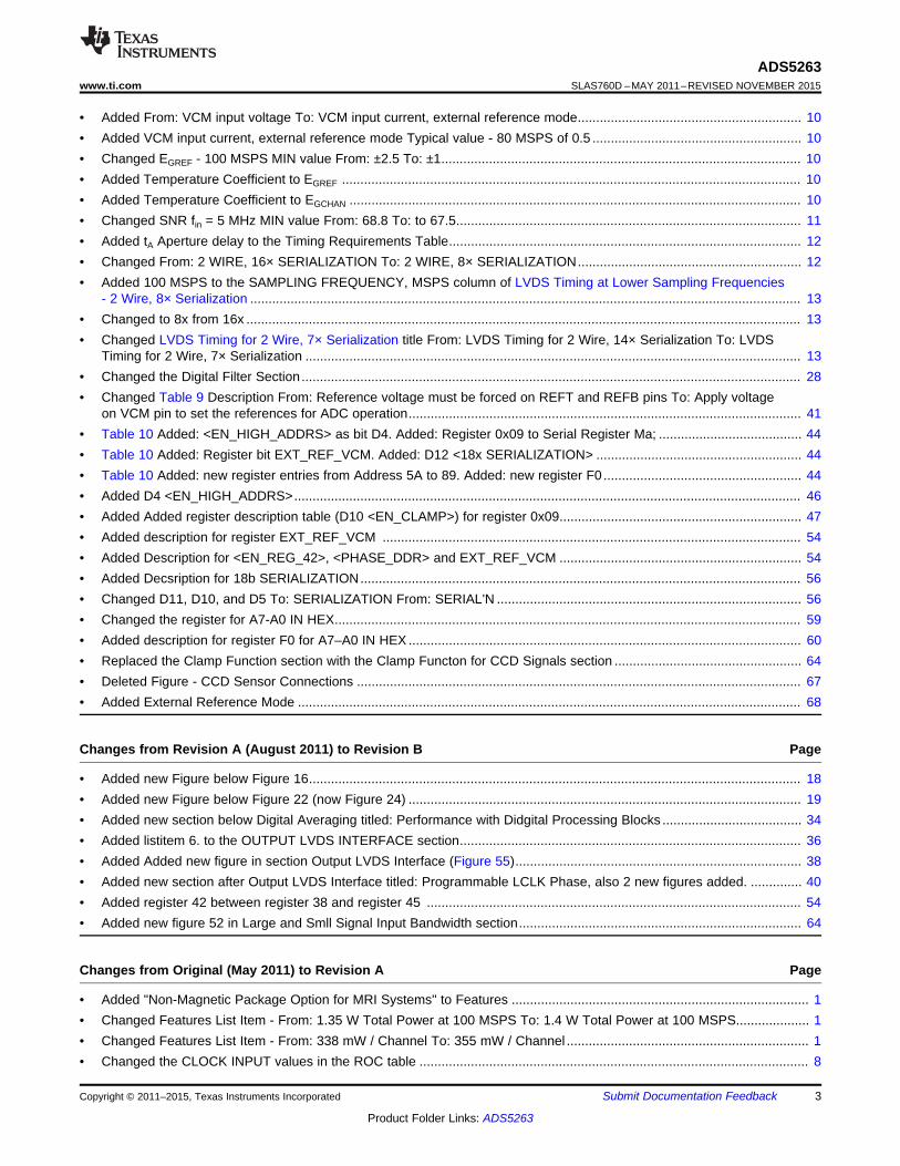
REFERENCE SERIAL INTERFACE IN1A_P IN1A_M CLKP CLKM VCM SCLK CSZ SDATA RESETZ ADS5263 14-Bit ADC INT/EXTZ REFT REFB OUT1P OUT1M AVDD AGND LVDD LGND PDN 16-Bit FE 16-Bit ADC IN1B_P IN1B_M IN4A_P IN4A_M IN4B_P IN4B_M CLOCK BUFFER CLOCKGEN ADC CONTROL ISET SDOUT ADC Clocking Sync Signal SYNC OUT2P OUT2M SERIALIZER SERIALIZER DIGITAL 14-Bit ADC OUT7P OUT7M 16-Bit FE OUT8P OUT8M SERIALIZER SERIALIZER DIGITAL LCLKP LCLKM ADCLKP ADCLKM BIT CLOCK 8X FRAME CLOCK 1X Product Folder Sample & Buy Technical Documents Tools & Software Support & Community ADS5263 SLAS760D – MAY 2011 – REVISED NOVEMBER 2015 ADS5263 Quad Channel 16-Bit, 100-MSPS High-SNR ADC 1 Features 2 Applications 1• Maximum Sample Rate: 100 MSPS • Medical Imaging – MRI • Programmable Device Resolution • Spectroscopy • CCD Imaging – Quad-Channel, 16-Bit, High-SNR Mode – Quad-Channel, 14-Bit, Low-Power Mode 3 Description • 16-Bit High-SNR Mode Using CMOS process technology and innovative – 1.4 W Total Power at 100 MSPS circuit techniques, the ADS5263 is designed to – 355 mW / Channel operate at low power and give very high SNR performance with a 4-Vpp full-scale input. Using a – 4 Vpp Full-scale Input low-noise 16-bit front-end stage followed by a 14-bit – 85-dBFS SNR at f in = 3 MHz, 100 MSPS ADC, the device gives 85-dBFS SNR up to 10 MHz • 14-Bit Low-Power Mode and better than 80-dBFS SNR up to 30 MHz. – 785 mW Total Power at 100 MSPS Device Information (1) – 195 mW/Channel PART NUMBER PACKAGE BODY SIZE (NOM) – 2-Vpp Full-Scale Input ADS5263 VQFN (64) 9.00 mm × 9.00 mm – 74-dBFS SNR at f in = 10 MHz (1) For all available packages, see the orderable addendum at – Integrated Clamp (for interfacing to CCD the end of the data sheet. sensors) ADS5263 Block Diagram • Low-Frequency Noise Suppression • Digital Processing Block – Programmable FIR Decimation Filters – Programmable Digital Gain: 0 dB to 12 dB – 2- or 4-Channel Averaging • Programmable Mapping Between ADC Input Channels and LVDS Output Pins—Eases Board Design • Variety of Test Patterns to Verify Data Capture by FPGA/Receiver • Serialized LVDS Outputs • Internal and External References • 3.3-V Analog Supply • 1.8-V Digital Supply • Recovers From 6-dB Overload Within 1 Clock Cycle • Package: – 9-mm × 9-mm 64-Pin QFN – Non-Magnetic Package Option for MRI Systems • CMOS Technology 1 An IMPORTANT NOTICE at the end of this data sheet addresses availability, warranty, changes, use in safety-critical applications, intellectual property matters and other important disclaimers. PRODUCTION DATA.

Welcome message from author
This document is posted to help you gain knowledge. Please leave a comment to let me know what you think about it! Share it to your friends and learn new things together.
Transcript
REFERENCE SERIALINTERFACE
IN1A_P
IN1A_M
CLKP
CLKM
VC
M
SC
LK
CS
Z
SD
AT
A
RE
SE
TZ
ADS5263
14-BitADC
INT
/EX
TZ
RE
FT
RE
FB
OUT1P
OUT1M
AV
DD
AG
ND
LV
DD
LG
ND
PD
N
16-BitFE
16-Bit ADC
IN1B_P
IN1B_M
IN4A_P
IN4A_M
IN4B_P
IN4B_M
CLOCKBUFFER CLOCKGEN
ADC CONTROL
ISE
T
SDOUT
ADC Clocking Sync Signal
SY
NC
OUT2P
OUT2M
SERIALIZER
SERIALIZER
DIGITAL
14-BitADC
OUT7P
OUT7M
16-BitFE
OUT8P
OUT8M
SERIALIZER
SERIALIZER
DIGITAL
LCLKP
LCLKM
ADCLKP
ADCLKM
BIT CLOCK 8X
FRAME CLOCK 1X
Product
Folder
Sample &Buy
Technical
Documents
Tools &
Software
Support &Community
ADS5263SLAS760D –MAY 2011–REVISED NOVEMBER 2015
ADS5263 Quad Channel 16-Bit, 100-MSPS High-SNR ADC1 Features 2 Applications1• Maximum Sample Rate: 100 MSPS • Medical Imaging – MRI• Programmable Device Resolution • Spectroscopy
• CCD Imaging– Quad-Channel, 16-Bit, High-SNR Mode– Quad-Channel, 14-Bit, Low-Power Mode
3 Description• 16-Bit High-SNR ModeUsing CMOS process technology and innovative– 1.4 W Total Power at 100 MSPS circuit techniques, the ADS5263 is designed to
– 355 mW / Channel operate at low power and give very high SNRperformance with a 4-Vpp full-scale input. Using a– 4 Vpp Full-scale Inputlow-noise 16-bit front-end stage followed by a 14-bit– 85-dBFS SNR at fin = 3 MHz, 100 MSPS ADC, the device gives 85-dBFS SNR up to 10 MHz
• 14-Bit Low-Power Mode and better than 80-dBFS SNR up to 30 MHz.– 785 mW Total Power at 100 MSPS
Device Information(1)– 195 mW/Channel
PART NUMBER PACKAGE BODY SIZE (NOM)– 2-Vpp Full-Scale InputADS5263 VQFN (64) 9.00 mm × 9.00 mm
– 74-dBFS SNR at fin = 10 MHz(1) For all available packages, see the orderable addendum at– Integrated Clamp (for interfacing to CCD the end of the data sheet.
sensors)ADS5263 Block Diagram• Low-Frequency Noise Suppression
• Digital Processing Block– Programmable FIR Decimation Filters– Programmable Digital Gain: 0 dB to 12 dB– 2- or 4-Channel Averaging
• Programmable Mapping Between ADC InputChannels and LVDS Output Pins—Eases BoardDesign
• Variety of Test Patterns to Verify Data Capture byFPGA/Receiver
• Serialized LVDS Outputs• Internal and External References• 3.3-V Analog Supply• 1.8-V Digital Supply• Recovers From 6-dB Overload Within 1 Clock
Cycle• Package:
– 9-mm × 9-mm 64-Pin QFN– Non-Magnetic Package Option for MRI
Systems• CMOS Technology
1
An IMPORTANT NOTICE at the end of this data sheet addresses availability, warranty, changes, use in safety-critical applications,intellectual property matters and other important disclaimers. PRODUCTION DATA.
ADS5263SLAS760D –MAY 2011–REVISED NOVEMBER 2015 www.ti.com
Table of Contents7.15 Reset Switching Characteristics ........................... 141 Features .................................................................. 17.16 Typical Characteristics .......................................... 172 Applications ........................................................... 1
8 Detailed Description ............................................ 253 Description ............................................................. 18.1 Overview ................................................................. 254 Revision History..................................................... 28.2 Functional Block Diagram ....................................... 265 Description (continued)......................................... 58.3 Feature Description................................................. 276 Pin Configuration and Functions ......................... 68.4 Device Functional Modes........................................ 417 Specifications......................................................... 8 8.5 Programming .......................................................... 43
7.1 Absolute Maximum Ratings ...................................... 8 8.6 Register Maps ......................................................... 447.2 ESD Ratings.............................................................. 8 9 Application and Implementation ........................ 627.3 Recommended Operating Conditions....................... 8
9.1 Application Information............................................ 627.4 Thermal Information .................................................. 99.2 Typical Applications ............................................... 707.5 Electrical Characteristics, Dynamic Performance –
10 Power Supply Recommendations ..................... 7116-Bit ADC ................................................................. 911 Layout................................................................... 727.6 Electrical Characteristics, General – 16-Bit ADC
Mode ........................................................................ 10 11.1 Layout Guidelines ................................................. 727.7 Electrical Characteristics, Dynamic Performance – 11.2 Layout Example .................................................... 73
14-Bit ADC ............................................................... 11 12 Device and Documentation Support ................. 747.8 Digital Characteristics ............................................. 12 12.1 Device Support...................................................... 747.9 Timing Requirements .............................................. 12 12.2 Community Resources.......................................... 757.10 LVDS Timing at Lower Sampling Frequencies - 2 12.3 Trademarks ........................................................... 76Wire, 8× Serialization............................................... 13
12.4 Electrostatic Discharge Caution............................ 767.11 LVDS Timing for 1 Wire 16× Serialization ............ 1312.5 Glossary ................................................................ 767.12 LVDS Timing for 2 Wire, 7× Serialization ............. 13
13 Mechanical, Packaging, and Orderable7.13 LVDS Timing for 1 Wire, 14× Serialization ........... 13Information ........................................................... 767.14 Serial Interface Timing Requirements................... 1413.1 Packaging ............................................................. 76
4 Revision HistoryNOTE: Page numbers for previous revisions may differ from page numbers in the current version.
Changes from Revision C (January 2013) to Revision D Page
• Added Register 57 in Register Maps ................................................................................................................................... 45• Added Register CB in Register Maps .................................................................................................................................. 45• Added Typical Applications section ...................................................................................................................................... 70• Added Layout section .......................................................................................................................................................... 72• Deleted Ordering Information table. See POA at the end of the data sheet. ...................................................................... 73
Changes from Revision B (October 2011) to Revision C Page
• Changed Pin 54 From: REFB To: NC .................................................................................................................................... 7• Changed Pin 55 From: REFC To: NC.................................................................................................................................... 7• Changed the VCM Pin description To: "Internal reference mode: Outputs the common-mode voltage (1.5 V) that
can be used externally to bias the analog input External reference mode: Apply voltage input that sets the referencefor ADC operation." From: "Outputs the common-mode voltage (1.5 V) that can be used externally to bias theanalog input pins." .................................................................................................................................................................. 7
• Added "Idle channel noise" To SNR....................................................................................................................................... 9• Added "Idle channel noise" To LSB ....................................................................................................................................... 9• Changed the INL values- 100 MSPS From: TYP = ±2.2 To: ±5, Added MAX = ±12............................................................. 9• to Changed the INL values- 80 MSPS From: TYP = ±2.2 To: ±5 .......................................................................................... 9• Added From: VCM common-mode output voltage To: VCM common-mode output voltage, Internal reference mode ..... 10• Added From: VCM output current capability To: VCM output current capability, Internal reference mode ......................... 10
2 Submit Documentation Feedback Copyright © 2011–2015, Texas Instruments Incorporated
Product Folder Links: ADS5263
ADS5263www.ti.com SLAS760D –MAY 2011–REVISED NOVEMBER 2015
• Added From: VCM input voltage To: VCM input current, external reference mode............................................................. 10• Added VCM input current, external reference mode Typical value - 80 MSPS of 0.5 ......................................................... 10• Changed EGREF - 100 MSPS MIN value From: ±2.5 To: ±1.................................................................................................. 10• Added Temperature Coefficient to EGREF ............................................................................................................................. 10• Added Temperature Coefficient to EGCHAN ........................................................................................................................... 10• Changed SNR fin = 5 MHz MIN value From: 68.8 To: to 67.5.............................................................................................. 11• Added tA Aperture delay to the Timing Requirements Table................................................................................................ 12• Changed From: 2 WIRE, 16× SERIALIZATION To: 2 WIRE, 8× SERIALIZATION............................................................. 12• Added 100 MSPS to the SAMPLING FREQUENCY, MSPS column of LVDS Timing at Lower Sampling Frequencies
- 2 Wire, 8× Serialization ...................................................................................................................................................... 13• Changed to 8x from 16x ....................................................................................................................................................... 13• Changed LVDS Timing for 2 Wire, 7× Serialization title From: LVDS Timing for 2 Wire, 14× Serialization To: LVDS
Timing for 2 Wire, 7× Serialization ....................................................................................................................................... 13• Changed the Digital Filter Section........................................................................................................................................ 28• Changed Table 9 Description From: Reference voltage must be forced on REFT and REFB pins To: Apply voltage
on VCM pin to set the references for ADC operation........................................................................................................... 41• Table 10 Added: <EN_HIGH_ADDRS> as bit D4. Added: Register 0x09 to Serial Register Ma; ....................................... 44• Table 10 Added: Register bit EXT_REF_VCM. Added: D12 <18x SERIALIZATION> ........................................................ 44• Table 10 Added: new register entries from Address 5A to 89. Added: new register F0 ...................................................... 44• Added D4 <EN_HIGH_ADDRS>.......................................................................................................................................... 46• Added Added register description table (D10 <EN_CLAMP>) for register 0x09.................................................................. 47• Added description for register EXT_REF_VCM .................................................................................................................. 54• Added Description for <EN_REG_42>, <PHASE_DDR> and EXT_REF_VCM .................................................................. 54• Added Decsription for 18b SERIALIZATION........................................................................................................................ 56• Changed D11, D10, and D5 To: SERIALIZATION From: SERIAL'N ................................................................................... 56• Changed the register for A7-A0 IN HEX............................................................................................................................... 59• Added description for register F0 for A7–A0 IN HEX ........................................................................................................... 60• Replaced the Clamp Function section with the Clamp Functon for CCD Signals section ................................................... 64• Deleted Figure - CCD Sensor Connections ......................................................................................................................... 67• Added External Reference Mode ......................................................................................................................................... 68
Changes from Revision A (August 2011) to Revision B Page
• Added new Figure below Figure 16...................................................................................................................................... 18• Added new Figure below Figure 22 (now Figure 24) ........................................................................................................... 19• Added new section below Digital Averaging titled: Performance with Didgital Processing Blocks ...................................... 34• Added listitem 6. to the OUTPUT LVDS INTERFACE section............................................................................................. 36• Added Added new figure in section Output LVDS Interface (Figure 55).............................................................................. 38• Added new section after Output LVDS Interface titled: Programmable LCLK Phase, also 2 new figures added. .............. 40• Added register 42 between register 38 and register 45 ...................................................................................................... 54• Added new figure 52 in Large and Smll Signal Input Bandwidth section............................................................................. 64
Changes from Original (May 2011) to Revision A Page
• Added "Non-Magnetic Package Option for MRI Systems" to Features ................................................................................. 1• Changed Features List Item - From: 1.35 W Total Power at 100 MSPS To: 1.4 W Total Power at 100 MSPS.................... 1• Changed Features List Item - From: 338 mW / Channel To: 355 mW / Channel .................................................................. 1• Changed the CLOCK INPUT values in the ROC table .......................................................................................................... 8
Copyright © 2011–2015, Texas Instruments Incorporated Submit Documentation Feedback 3
Product Folder Links: ADS5263

ADS5263SLAS760D –MAY 2011–REVISED NOVEMBER 2015 www.ti.com
• Changed the ELECTRICAL CHARACTERISTICS, DYNAMIC PERFORMANCE – 16-BIT ADC table................................. 9• Changed the ELECTRICAL CHARACTERISTICS, GENERAL – 16-BIT ADC MODE table ............................................... 10• Added the ELECTRICAL CHARACTERISTICS, DYNAMIC PERFORMANCE – 14-BIT ADC table................................... 11• Changed the values in DIGITAL OUTPUTS – LVDS INTERFACE ..................................................................................... 12• Added LVDS Timing for 1 Wire 16× Serialization, LVDS Timing for 2 Wire, 7× Serialization, and LVDS Timing for 1
Wire, 14× Serialization.......................................................................................................................................................... 13• Added Figure 25, Figure 26, and Figure 27 ......................................................................................................................... 20• Added section - Large and Small Signal Input Bandwidth ................................................................................................... 63• Added Section - Board Design Considerations .................................................................................................................... 73• Added Package Marking ADS5263NM and Ordering Number ADS5263IRGC-NM ............................................................ 73• Added Section - DEFINITION OF SPECIFICATIONS ......................................................................................................... 74• Added Section - Packaging .................................................................................................................................................. 76
4 Submit Documentation Feedback Copyright © 2011–2015, Texas Instruments Incorporated
Product Folder Links: ADS5263

ADS5263www.ti.com SLAS760D –MAY 2011–REVISED NOVEMBER 2015
5 Description (continued)ADS5263 has a 14-bit low power mode, where it operates as a quad-channel 14-bit ADC. The 16-bit front-endstage is powered down and the part consumes almost half the power, compared to the 16-bit mode. The 14-bitmode supports a 2-Vpp full-scale input signal, with typical 74-dBFS SNR. The ADS5263 can be dynamicallyswitched between the two resolution modes. This allows systems to use the same part in a high-resolution, high-power mode or a low-resolution, low-power mode.
The device also has a digital processing block that integrates several commonly used digital functions, such asdigital gain (up to 12 dB). It includes a digital filter module that has built-in decimation filters (with low-pass, high-pass and band-pass characteristics). The decimation rate is also programmable (by 2, by 4, or by 8). This makesit very useful for narrow-band applications, where the filters can be used to improve SNR and knock-offharmonics, while at the same time reducing the output data rate.
The device includes an averaging mode where two channels (or even four channels) can be averaged to improveSNR. A very unique feature is the programmable mapper module that allows flexible mapping between the inputchannels and the LVDS output pins. This helps to greatly reduce the complexity of LVDS output routing and canpotentially result in cheaper system boards by reducing the number of PCB layers. Specification of device is overindustrial temperature range of –40°C to 85°C.
Copyright © 2011–2015, Texas Instruments Incorporated Submit Documentation Feedback 5
Product Folder Links: ADS5263
48
47
46
45
44
43
42
41
40
39
38
37
36
35
34
33
1
2
3
4
5
6
7
8
9
10
11
12
13
14
15
1617
64
18
63
19
62
20
61
21
60
22
59
23
58
24
57
25
56
26
55
27
54
28
53
29
52
30
51
31
50
32
49
P0056-19
OUT1P
OUT1M
OU
T5P
OU
T5M
CS
Z
AV
DD
ISE
T
VC
M
IN2A_P
IN2A_M
LC
LK
M
AGND
IN4B_P
IN4B_M
AGND
IN4A_P
IN4A_M
SY
NC
CL
KP
RE
SE
TZ
AGND
OU
T7
P
OU
T7M
IN3A_P
IN3A_M
NC
AV
DD
IN2B_P
AGND
LGND
AGND
IN3B_P
IN3B_M
IN2B_M
LGND
PD
LGND
LC
LK
P
OUT8P
OUT8M
LVDD
OU
T6P
OU
T6M
OU
T2P
OU
T2M
OU
T3P
OU
T3M
OU
T4P
OU
T4M
AD
CLK
P
AD
CLK
M
IN1A_P
IN1A_M
AGND
IN1B_P
IN1B_M
AGND
CLK
M
SD
ATA
SC
LK
AV
DD
SD
OU
T
NC
INT
/EX
TZ
Thermal Pad64 QFN
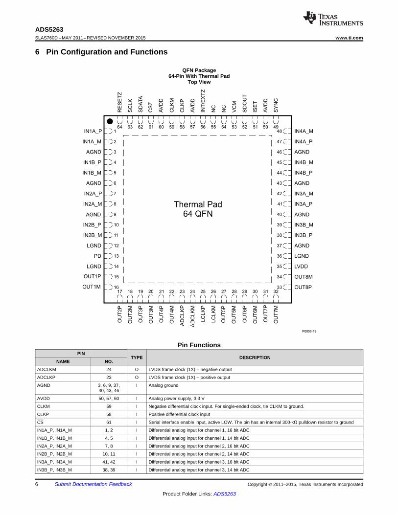
ADS5263SLAS760D –MAY 2011–REVISED NOVEMBER 2015 www.ti.com
6 Pin Configuration and Functions
QFN Package64-Pin With Thermal Pad
Top View
Pin FunctionsPIN
TYPE DESCRIPTIONNAME NO.
ADCLKM 24 O LVDS frame clock (1X) – negative output
ADCLKP 23 O LVDS frame clock (1X) – positive output
AGND 3, 6, 9, 37, I Analog ground40, 43, 46
AVDD 50, 57, 60 I Analog power supply, 3.3 V
CLKM 59 I Negative differential clock input. For single-ended clock, tie CLKM to ground.
CLKP 58 I Positive differential clock input
CS 61 I Serial interface enable input, active LOW. The pin has an internal 300-kΩ pulldown resistor to ground
IN1A_P, IN1A_M 1, 2 I Differential analog input for channel 1, 16 bit ADC
IN1B_P, IN1B_M 4, 5 I Differential analog input for channel 1, 14 bit ADC
IN2A_P, IN2A_M 7, 8 I Differential analog input for channel 2, 16 bit ADC
IN2B_P, IN2B_M 10, 11 I Differential analog input for channel 2, 14 bit ADC
IN3A_P, IN3A_M 41, 42 I Differential analog input for channel 3, 16 bit ADC
IN3B_P, IN3B_M 38, 39 I Differential analog input for channel 3, 14 bit ADC
6 Submit Documentation Feedback Copyright © 2011–2015, Texas Instruments Incorporated
Product Folder Links: ADS5263
ADS5263www.ti.com SLAS760D –MAY 2011–REVISED NOVEMBER 2015
Pin Functions (continued)PIN
TYPE DESCRIPTIONNAME NO.
IN4A_P, IN4A_M 47, 48 I Differential analog input for channel 4, 16 bit ADC
IN4B_P, IN4B_M 44, 45 I Differential analog input for channel 4, 14 bit ADC
INT/EXT 56 I Internal/external reference mode select inputLogic HIGH –internal referenceLogic LOW – external reference
ISET 51 I Bias pin – 56.2 kΩ resistor (1% tolerance value) to ground
LCLKM 26 O LVDS bit clock (8X) – negative output
LCLKP 25 O LVDS bit clock (8X) – positive output
LGND 12, 14, 36 I Digital ground
LVDD 35 I Digital and I/O power supply, 1.8 V
OUT1P, OUT1M 15, 16 O Wire 1, channel 1 LVDS differential output
OUT2P, OUT2M 17, 18 O Wire 2, channel 1 LVDS differential output
OUT3P, OUT3M 19, 20 O Wire 1, channel 2, LVDS differential output
OUT4P, OUT4M 21, 22 O Wire 2, channel 2 LVDS differential output
OUT5P, OUT5M 27, 28 O Wire 1, channel 3 LVDS differential output
OUT6P, OUT6M 29, 30 O Wire 2, channel 3 LVDS differential output
OUT7P, OUT7M 31, 32 O Wire 1, channel 4 LVDS differential output
OUT8P, OUT8M 33, 34 O Wire 2, channel 4 LVDS differential output
PD 13 I Power-down input
NC 54, 55 Do not connect
RESET 64 I Serial interface RESET input, active LOW.When using the serial interface mode, the user must initialize internal registers through hardwareRESET by applying a low-going pulse on this pin or by using software reset option. See the SerialInterface section.
SCLK 63 I Serial interface clock input. The pin has an internal 300-kΩ pulldown resistor.
SDATA 62 I Serial interface data input. The pin has an internal 300-kΩ pulldown resistor.
SDOUT 52 O Serial register readoutThis pin is in the high-impedance state after reset. When the <READOUT> bit is set, the SDOUT pinbecomes active. This is a CMOS digital output running from the AVDD supply.
SYNC 49 I Input signal to synchronize channels and chips when used with reduced output data ratesAlternate function: Clamp signal input (14-bit ADC mode only)
VCM 53 IO Internal reference mode: Outputs the common-mode voltage (1.5 V) that can be used externally to biasthe analog input.External reference mode: Apply voltage input that sets the reference for ADC operation.
Copyright © 2011–2015, Texas Instruments Incorporated Submit Documentation Feedback 7
Product Folder Links: ADS5263
ADS5263SLAS760D –MAY 2011–REVISED NOVEMBER 2015 www.ti.com
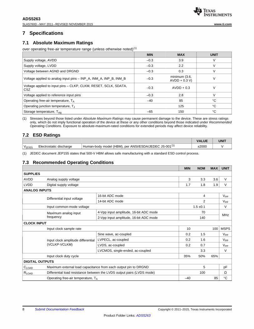
7 Specifications
7.1 Absolute Maximum Ratingsover operating free-air temperature range (unless otherwise noted) (1)
MIN MAX UNITSupply voltage, AVDD –0.3 3.9 VSupply voltage, LVDD –0.3 2.2 VVoltage between AGND and DRGND –0.3 0.3 V
minimum (3.6,Voltage applied to analog input pins – INP_A, INM_A, INP_B, INM_B –0.3 VAVDD + 0.3 V)Voltage applied to input pins – CLKP, CLKM, RESET, SCLK, SDATA, –0.3 AVDD + 0.3 VCSZVoltage applied to reference input pins –0.3 2.8 VOperating free-air temperature, TA –40 85 °COperating junction temperature, TJ 125 °CStorage temperature, Tstg –65 150 °C
(1) Stresses beyond those listed under Absolute Maximum Ratings may cause permanent damage to the device. These are stress ratingsonly, which do not imply functional operation of the device at these or any other conditions beyond those indicated under RecommendedOperating Conditions. Exposure to absolute-maximum-rated conditions for extended periods may affect device reliability.
7.2 ESD RatingsVALUE UNIT
V(ESD) Electrostatic discharge Human-body model (HBM), per ANSI/ESDA/JEDEC JS-001 (1) ±2000 V
(1) JEDEC document JEP155 states that 500-V HBM allows safe manufacturing with a standard ESD control process.
7.3 Recommended Operating ConditionsMIN NOM MAX UNIT
SUPPLIESAVDD Analog supply voltage 3 3.3 3.6 VLVDD Digital supply voltage 1.7 1.8 1.9 VANALOG INPUTS
16-bit ADC mode 4 VPPDifferential input voltage14-bit ADC mode 2 VPP
Input common-mode voltage 1.5 ±0.1 V4-Vpp input amplitude, 16-bit ADC mode 70Maximum analog input MHzfrequency 2-Vpp input amplitude, 16-bit ADC mode 140
CLOCK INPUTInput clock sample rate 10 100 MSPS
Sine wave, ac-coupled 0.2 1.5 VPP
LVPECL, ac-coupled 0.2 1.6 VPPInput clock amplitude differential(VCLKP-VCLKM) LVDS, ac-coupled 0.2 0.7 VPP
LVCMOS, single-ended, ac-coupled 3.3 VInput clock duty cycle 35% 50% 65%
DIGITAL OUTPUTSCLOAD Maximum external load capacitance from each output pin to DRGND 5 pFRLOAD Differential load resistance between the LVDS output pairs (LVDS mode) 100 Ω
Operating free-air temperature, TA –40 85 °C
8 Submit Documentation Feedback Copyright © 2011–2015, Texas Instruments Incorporated
Product Folder Links: ADS5263

ADS5263www.ti.com SLAS760D –MAY 2011–REVISED NOVEMBER 2015
7.4 Thermal InformationADS5263
THERMAL METRIC (1) RGC (VQFN) UNIT64 PINS
RθJA Junction-to-ambient thermal resistance 20.6 °C/WRθJC(top) Junction-to-case (top) thermal resistance 6.1 °C/WRθJB Junction-to-board thermal resistance 2.7 °C/WψJT Junction-to-top characterization parameter 0.2 °C/WψJB Junction-to-board characterization parameter 2.6 °C/WRθJC(bot) Junction-to-case (bottom) thermal resistance 0.4 °C/W
(1) For more information about traditional and new thermal metrics, see the Semiconductor and IC Package Thermal Metrics applicationreport, SPRA953.
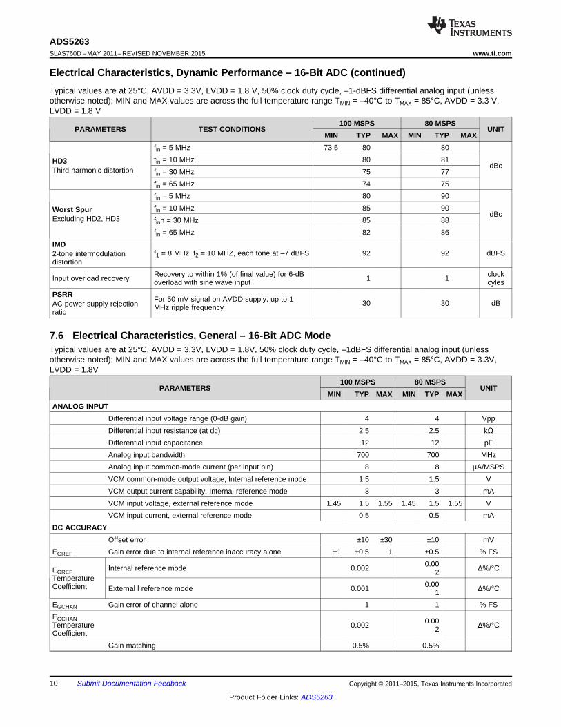
7.5 Electrical Characteristics, Dynamic Performance – 16-Bit ADCTypical values are at 25°C, AVDD = 3.3V, LVDD = 1.8 V, 50% clock duty cycle, –1-dBFS differential analog input (unlessotherwise noted); MIN and MAX values are across the full temperature range TMIN = –40°C to TMAX = 85°C, AVDD = 3.3 V,LVDD = 1.8 V
100 MSPS 80 MSPSPARAMETERS TEST CONDITIONS UNIT
MIN TYP MAX MIN TYP MAXSNR With inputs tied to common-mode VCM 87.5 87.5 dBFSIdle channel noiseLSB With inputs tied to common-mode VCM 0.98 0.98 rmsIdle channel noise
fin = 5 MHz at 25°C 81 84.5 85.5fin = 5 MHz across temperature 80
SNR fin = 10 MHz 84.6 85.3 dBFSSignal-to-noise ratiofin = 30 MHz 82.7 83.1fin = 65 MHz 78.9 79.4fin = 5 MHz 76.6 78.2 78.8
SINAD fin = 10 MHz 77.5 79dBFSSignal-to-noise and distortion
finn = 30 MHz 74.8 76ratiofin = 65 MHz 71.6 72.5
ENOB fin = 5 MHz 12.7 12.8 LSBEffective number of bitsDNL fin = 5 MHz ±0.1 ±0.1 LSBDifferential non-linearityINL fin = 5 MHz Changed the INL values 100 MSPS ±5 ±12 ±5 LSBFrom: TYP = ±2.2 To: ±5, Added MAX = ±12Integrated non-linearity
fin = 5 MHz 73.5 80 80fin = 10 MHz 80 81SFDR dBcSpurious-free dynamic range fin = 30 MHz 76 77fin = 65 MHz 74 75fin = 5 MHz 72.5 78 78.8fin = 10 MHz 77.4 79.2THD dBcTotal harominc distortion fin = 30 MHz 74.5 76fin = 65 MHz 71.4 72.4fin = 5 MHz 73.5 83.5 85fin = 10 MHz 81 84HD2 dBcSecond harmonic Distortion fin = 30 MHz 80 83fin = 65 MHz 75 76
Copyright © 2011–2015, Texas Instruments Incorporated Submit Documentation Feedback 9
Product Folder Links: ADS5263
ADS5263SLAS760D –MAY 2011–REVISED NOVEMBER 2015 www.ti.com
Electrical Characteristics, Dynamic Performance – 16-Bit ADC (continued)Typical values are at 25°C, AVDD = 3.3V, LVDD = 1.8 V, 50% clock duty cycle, –1-dBFS differential analog input (unlessotherwise noted); MIN and MAX values are across the full temperature range TMIN = –40°C to TMAX = 85°C, AVDD = 3.3 V,LVDD = 1.8 V
100 MSPS 80 MSPSPARAMETERS TEST CONDITIONS UNIT
MIN TYP MAX MIN TYP MAXfin = 5 MHz 73.5 80 80fin = 10 MHz 80 81HD3 dBcThird harmonic distortion fin = 30 MHz 75 77fin = 65 MHz 74 75fin = 5 MHz 80 90fin = 10 MHz 85 90Worst Spur dBcExcluding HD2, HD3 finn = 30 MHz 85 88fin = 65 MHz 82 86
IMDf1 = 8 MHz, f2 = 10 MHZ, each tone at –7 dBFS 92 92 dBFS2-tone intermodulation
distortionRecovery to within 1% (of final value) for 6-dB clockInput overload recovery 1 1overload with sine wave input cyles
PSRR For 50 mV signal on AVDD supply, up to 1 30 30 dBAC power supply rejection MHz ripple frequencyratio
7.6 Electrical Characteristics, General – 16-Bit ADC ModeTypical values are at 25°C, AVDD = 3.3V, LVDD = 1.8V, 50% clock duty cycle, –1dBFS differential analog input (unlessotherwise noted); MIN and MAX values are across the full temperature range TMIN = –40°C to TMAX = 85°C, AVDD = 3.3V,LVDD = 1.8V
100 MSPS 80 MSPSPARAMETERS UNIT
MIN TYP MAX MIN TYP MAXANALOG INPUT
Differential input voltage range (0-dB gain) 4 4 VppDifferential input resistance (at dc) 2.5 2.5 kΩDifferential input capacitance 12 12 pFAnalog input bandwidth 700 700 MHzAnalog input common-mode current (per input pin) 8 8 µA/MSPSVCM common-mode output voltage, Internal reference mode 1.5 1.5 VVCM output current capability, Internal reference mode 3 3 mAVCM input voltage, external reference mode 1.45 1.5 1.55 1.45 1.5 1.55 VVCM input current, external reference mode 0.5 0.5 mA
DC ACCURACYOffset error ±10 ±30 ±10 mV
EGREF Gain error due to internal reference inaccuracy alone ±1 ±0.5 1 ±0.5 % FS0.00Internal reference mode 0.002 Δ%/°CEGREF 2
Temperature0.00Coefficient External l reference mode 0.001 Δ%/°C1
EGCHAN Gain error of channel alone 1 1 % FSEGCHAN 0.00Temperature 0.002 Δ%/°C2Coefficient
Gain matching 0.5% 0.5%
10 Submit Documentation Feedback Copyright © 2011–2015, Texas Instruments Incorporated
Product Folder Links: ADS5263

ADS5263www.ti.com SLAS760D –MAY 2011–REVISED NOVEMBER 2015
Electrical Characteristics, General – 16-Bit ADC Mode (continued)Typical values are at 25°C, AVDD = 3.3V, LVDD = 1.8V, 50% clock duty cycle, –1dBFS differential analog input (unlessotherwise noted); MIN and MAX values are across the full temperature range TMIN = –40°C to TMAX = 85°C, AVDD = 3.3V,LVDD = 1.8V
100 MSPS 80 MSPSPARAMETERS UNIT
MIN TYP MAX MIN TYP MAXPOWER SUPPLYIAVDD Analog supply current 370 390 290 mA
Digital and output buffer supply current with 100-Ω externalILVDD 110 150 100 mALVDS terminationAnalog power 1.22 0.96 WDigital power 0.2 0.18 WGlobal power down 63 110 63 mWStandby 208 250 208 mW
7.7 Electrical Characteristics, Dynamic Performance – 14-Bit ADCTypical values are at 25°C, AVDD = 3.3V, LVDD = 1.8 V, 50% clock duty cycle, –1-dBFS differential analog input (unlessotherwise noted); MIN and MAX values are across the full temperature range TMIN = –40°C to TMAX = 85°C, AVDD = 3.3 V,LVDD = 1.8 V
100 MSPSPARAMETERS TEST CONDITIONS UNIT
MIN TYP MAXfin = 5 MHz 67.5 74
SNR finv = 30 MHz 73 dBFSSignal-to-noise ratiofin = 65 MHz 71.3fin = 5 MHz 65.8 73.5
SINAD fin = 30 MHz 71.9 dBFSSignal-to-noise and distortion ratiofinn = 65 MHz 70.3fin = 5 MHz 71.8 85
SFDR fin = 30 MHz 81 dBcSpurious-free dynamic rangefin = 65 MHz 78fin = 5 MHz 69 83.5
THD fin = 30 MHz 78 dBcTotal harmonic distortionfin = 65 MHz 76.5fin = 5 MHz 71.8 92
HD2 fin = 30 MHz 84 dBcSecond harmonic Distortionfin = 65 MHz 80fin = 5 MHz 71.8 85
HD3 fin = 30 MHz 81 dBcThird harmonic distortionfin = 65 MHz 78
Copyright © 2011–2015, Texas Instruments Incorporated Submit Documentation Feedback 11
Product Folder Links: ADS5263

ADS5263SLAS760D –MAY 2011–REVISED NOVEMBER 2015 www.ti.com
7.8 Digital CharacteristicsThe DC specifications refer to the condition where the digital outputs are not switching, but are permanently at a valid logiclevel 0 or 1. AVDD = 3.3V, LVDD = 1.8V
PARAMETER TEST CONDITIONS MIN TYP MAX UNITDIGITAL INPUTS – RESET, SCLK, SDATA, CS, PDN, SYNC, INT/EXT
All digital inputs support 1.8-V andVIH High-level input voltage 1.3 V3.3-V CMOS logic levels.VIL Low-level input voltage 0.4 V
High-level input SDATA, SCLK, CS (1) VHIGH = 1.8 VIIH 5 μAcurrentLow-level input SDATA, SCLK, CS VLOW = 0 VIIL 0 μAcurrent
DIGITAL CMOS OUTPUT – SDOUTVOH High-level output voltage IOH = 100 µA AVDD – 0.05 VVOL Low-level output voltage IOL = 100 µA 0.05 VDIGITAL OUTPUTS – LVDS INTERFACE (OUT1P/M TO OUT8P/M, ADCLKP/M, LCLKP/M)VODH High-level output differential voltage With external 100-Ω termination 275 370 465 mVVODL Low-level output differential voltage With external 100-Ω termination –465 –370 –275 mVVOCM Output common-mode voltage 1000 1200 1400 mV
(1) CS, SDATA, SCLK have internal 300-kΩ pulldown resistor.
7.9 Timing Requirements (1)
Typical values are at 25°C, AVDD = 3.3 V, LVDD = 1.8 V, sampling frequency = 100 MSPS, sine wave input clock = 1.5 Vppclock amplitude, CLOAD = 5 pF (2), RLOAD = 100 Ω (3), unless otherwise noted. MIN and MAX values are across the fulltemperature range, TMIN = –40°C to TMAX = 85°C, AVDD = 3.3 V, LVDD = 1.7 V to 1.9 V
MIN TYP MAX UNITtj Aperture jitter 220 fs rms
Time delay between rising edge of input clock and the actualtA Aperture delay 3 nssampling instantTime to valid data after coming out of STANDBY mode 10
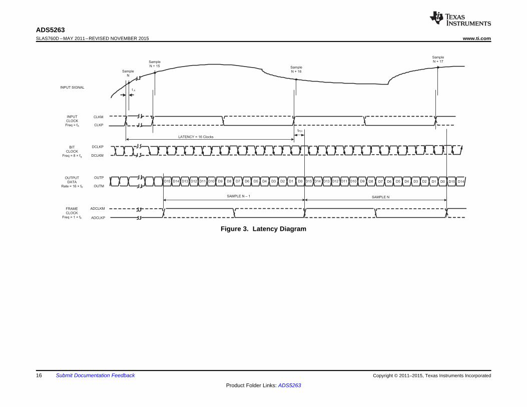
Wake-up time μsTime to valid data after coming out of global power down 60Latency of ADC alone, excludes the delay from input clock to ClockADC latency 16output clock (tPDI), Figure 3 cycles
2 WIRE, 8× SERIALIZATION (4)
tsu Data setup time Data valid (5) to zero-crossing of LCLKP 0.23 nsth Data hold time Zero-crossing of LCLKP to data becoming invalid (5) 0.31 ns
Clock propagation Input clock rising edge crossover to output frame clock ADCLKPtPDI 6.8 8.8 10.8 nsdelay rising edge crossover, tPDI = (ts/4) + tdelay
Variation of tPDI Between two devices at same temperature and LVDD supply ±0.6 nsLVDS bit clock duty Duty cycle of differential clock, (LCLKP-LCLKM) 50%cycle
Rise time measured from –100 mV to 100 mV,tRISE Data rise time, 0.17 nsFall time measured from 100 mV to –100 mVtFALL Data fall time 10 MSPS ≤ Sampling frequency ≤ 100 MSPSRise time measured from –100 mV to 100 mVtCLKRISE Output clock rise time, 0.2 nsFall time measured from 100 mV to –100 mVtCLKFALL Output clock fall time 10 MSPS ≤ Sampling frequency ≤ 100 MSPS
(1) Timing parameters are ensured by design and characterization and not tested in production.(2) CLOAD is the effective external single-ended load capacitance between each output pin and ground.(3) RLOAD is the differential load resistance between the LVDS output pair.(4) Measurements are done with a transmission line of 100-Ω characteristic impedance between the device and the load. Setup and hold
time specifications take into account the effect of jitter on the output data and clock.(5) Data valid refers to logic HIGH of 100 mV and logic LOW of –100 mV.
12 Submit Documentation Feedback Copyright © 2011–2015, Texas Instruments Incorporated
Product Folder Links: ADS5263
ADS5263www.ti.com SLAS760D –MAY 2011–REVISED NOVEMBER 2015
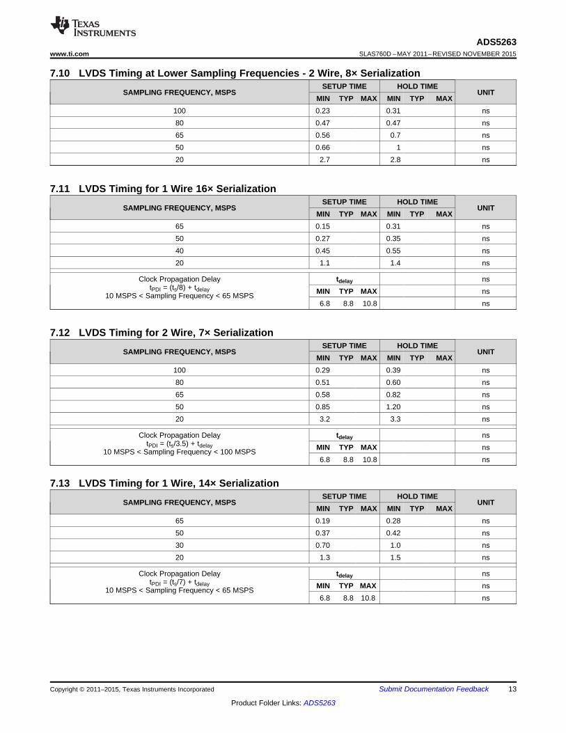
7.10 LVDS Timing at Lower Sampling Frequencies - 2 Wire, 8× SerializationSETUP TIME HOLD TIME
SAMPLING FREQUENCY, MSPS UNITMIN TYP MAX MIN TYP MAX
100 0.23 0.31 ns80 0.47 0.47 ns65 0.56 0.7 ns50 0.66 1 ns20 2.7 2.8 ns
7.11 LVDS Timing for 1 Wire 16× SerializationSETUP TIME HOLD TIME
SAMPLING FREQUENCY, MSPS UNITMIN TYP MAX MIN TYP MAX
65 0.15 0.31 ns50 0.27 0.35 ns40 0.45 0.55 ns20 1.1 1.4 ns
Clock Propagation Delay tdelay nstPDI = (ts/8) + tdelay MIN TYP MAX ns10 MSPS < Sampling Frequency < 65 MSPS
6.8 8.8 10.8 ns
7.12 LVDS Timing for 2 Wire, 7× SerializationSETUP TIME HOLD TIME
SAMPLING FREQUENCY, MSPS UNITMIN TYP MAX MIN TYP MAX
100 0.29 0.39 ns80 0.51 0.60 ns65 0.58 0.82 ns50 0.85 1.20 ns20 3.2 3.3 ns
Clock Propagation Delay tdelay nstPDI = (ts/3.5) + tdelay MIN TYP MAX ns10 MSPS < Sampling Frequency < 100 MSPS
6.8 8.8 10.8 ns
7.13 LVDS Timing for 1 Wire, 14× SerializationSETUP TIME HOLD TIME
SAMPLING FREQUENCY, MSPS UNITMIN TYP MAX MIN TYP MAX
65 0.19 0.28 ns50 0.37 0.42 ns30 0.70 1.0 ns20 1.3 1.5 ns
Clock Propagation Delay tdelay nstPDI = (ts/7) + tdelay MIN TYP MAX ns10 MSPS < Sampling Frequency < 65 MSPS
6.8 8.8 10.8 ns
Copyright © 2011–2015, Texas Instruments Incorporated Submit Documentation Feedback 13
Product Folder Links: ADS5263
POWER SUPPLY
AVDD,DRVDD
RESET
SEN
t1
t2
t3
ADS5263SLAS760D –MAY 2011–REVISED NOVEMBER 2015 www.ti.com
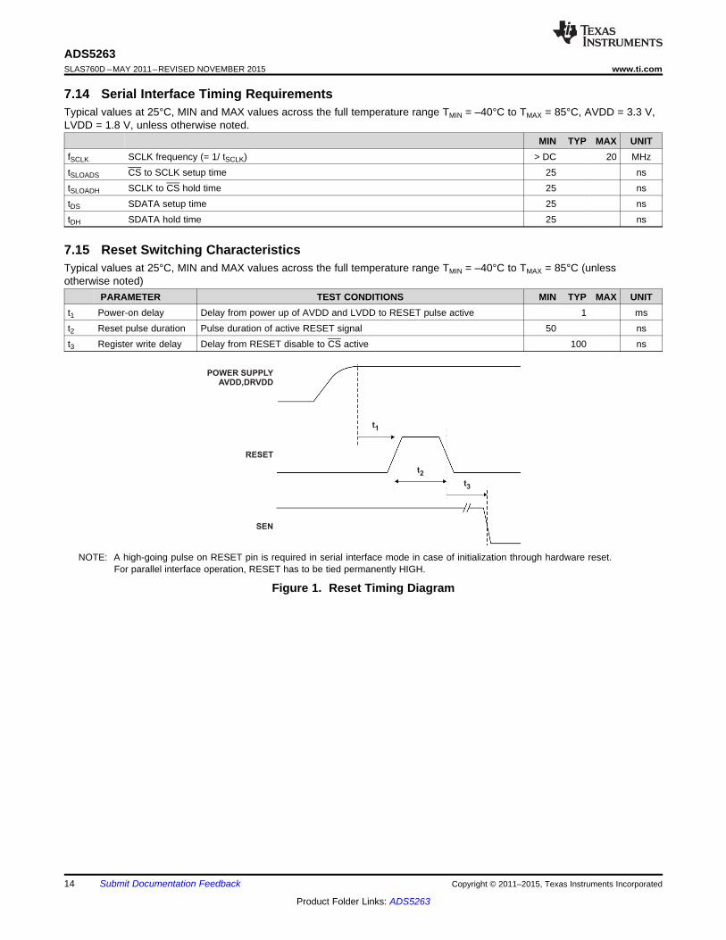
7.14 Serial Interface Timing RequirementsTypical values at 25°C, MIN and MAX values across the full temperature range TMIN = –40°C to TMAX = 85°C, AVDD = 3.3 V,LVDD = 1.8 V, unless otherwise noted.
MIN TYP MAX UNITfSCLK SCLK frequency (= 1/ tSCLK) > DC 20 MHztSLOADS CS to SCLK setup time 25 nstSLOADH SCLK to CS hold time 25 nstDS SDATA setup time 25 nstDH SDATA hold time 25 ns
7.15 Reset Switching CharacteristicsTypical values at 25°C, MIN and MAX values across the full temperature range TMIN = –40°C to TMAX = 85°C (unlessotherwise noted)
PARAMETER TEST CONDITIONS MIN TYP MAX UNITt1 Power-on delay Delay from power up of AVDD and LVDD to RESET pulse active 1 mst2 Reset pulse duration Pulse duration of active RESET signal 50 nst3 Register write delay Delay from RESET disable to CS active 100 ns
NOTE: A high-going pulse on RESET pin is required in serial interface mode in case of initialization through hardware reset.For parallel interface operation, RESET has to be tied permanently HIGH.
Figure 1. Reset Timing Diagram
14 Submit Documentation Feedback Copyright © 2011–2015, Texas Instruments Incorporated
Product Folder Links: ADS5263

LCLKMLCLKM
LCLKPLCLKP
OUTPUT DATA
&FRAME CLK Dn* Dn+1*
t PDItPDI
CLKMCLKM
CLKPCLKP
BIT CLOCK4X
BIT CLOCK4X
INPUT CLOCK1X
INPUT CLOCK1X
ADCLKMADCLKM
ADCLKPADCLKP
FRAME CLOCKX
FRAME CLOCK0.5X
h
t su t h
OUT 1, OUT 2
OUT 3, OUT 4
OUT 5, OUT 6
OUT 7, OUT 8
tsu
tsu
th
th tsu th
ADS5263www.ti.com SLAS760D –MAY 2011–REVISED NOVEMBER 2015
Figure 2. LVDS Timing
Copyright © 2011–2015, Texas Instruments Incorporated Submit Documentation Feedback 15
Product Folder Links: ADS5263
INPUT
CLOCK
Freq = fS
DCLKP
DCLKM
OUTPUT
DATA
Rate = 16 × fS
INPUT SIGNAL
Sample
N
t A
CLKM
CLKP
D15 D14 D13 D12 D11 D10 D9 D8 D7 D6 D5 D4 D3 D2 D1 D0 D15 D14 D13 D12 D11 D10 D9 D8
ADCLKM
ADCLKP
BIT
CLOCK
Freq = 8 × f
FRAME
CLOCK
Freq = 1 × fS
OUTP
OUTM
SAMPLE N – 1 SAMPLE N
LATENCY = 16 Clocks
Sample
N + 16
Sample
N + 15
Sample
N + 17
tPDI
D5 D4 D3 D2D7 D6 D1 D0 D15 D14
S
ADS5263SLAS760D –MAY 2011–REVISED NOVEMBER 2015 www.ti.com
Figure 3. Latency Diagram
16 Submit Documentation Feedback Copyright © 2011–2015, Texas Instruments Incorporated
Product Folder Links: ADS5263

−140
−130
−120
−110
−100
−90
−80
−70
−60
−50
−40
−30
−20
−10
0
0 5 10 15 20 25 30 35 40
Frequency (MHz)
Am
plit
ud
e (
dB
FS
)
SNR =85.7 dBFS
SINAD = 81.4 dBFS
THD = 82.4 dBc
SFDR = 83.1 dBc
G003
−140
−130
−120
−110
−100
−90
−80
−70
−60
−50
−40
−30
−20
−10
0
0 5 10 15 20 25 30 35 40
Frequency (MHz)
Am
plit
ud
e (
dB
FS
)
SNR = 84.8 dBFS
SINAD = 79.4 dBFS
THD = 79.9 dBc
SFDR = 82.7dBc
G004
−140
−130
−120
−110
−100
−90
−80
−70
−60
−50
−40
−30
−20
−10
0
0 5 10 15 20
Frequency (MHz)
Am
plit
ud
e (
dB
FS
)
SNR = 85.6 dBFS
SINAD = 83.5 dBFS
THD = 86.7 dBc
SFDR = 89.7 dBc
G001
−140
−130
−120
−110
−100
−90
−80
−70
−60
−50
−40
−30
−20
−10
0
0 5 10 15 20
Frequency (MHz)
Am
plit
ud
e (
dB
FS
)SNR = 84.7 dBFS
SINAD = 81.6 dBFS
SFDR = 84.9 dBc
THD = 83.4 dBc
G002
GND
Logic 0
OUTP
OUTM
GND
Logic 0V = -350 mV*ODL
Logic 0V = +350 mV*ODH
VOCM
*With external 100- terminationW
ADS5263www.ti.com SLAS760D –MAY 2011–REVISED NOVEMBER 2015
Figure 4. LVDS Output Voltage Levels
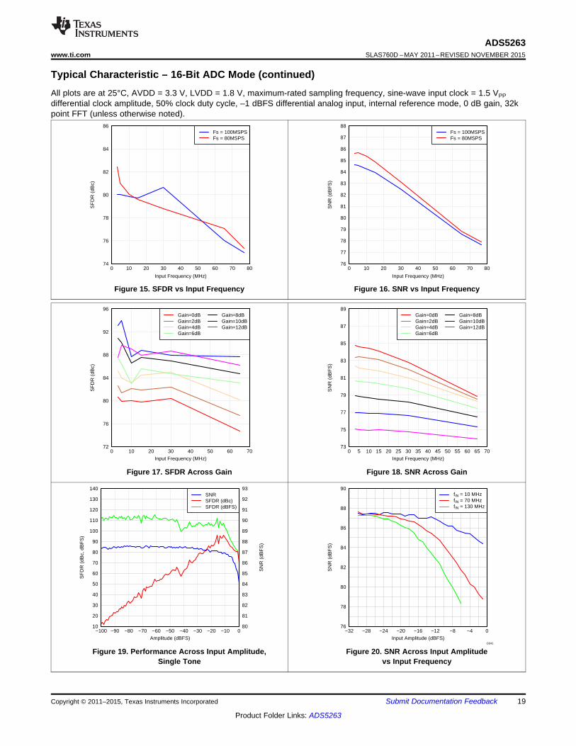
7.16 Typical Characteristics
7.16.1 Typical Characteristic – 16-Bit ADC ModeAll plots are at 25°C, AVDD = 3.3 V, LVDD = 1.8 V, maximum-rated sampling frequency, sine-wave input clock = 1.5 VPPdifferential clock amplitude, 50% clock duty cycle, –1 dBFS differential analog input, internal reference mode, 0 dB gain, 32kpoint FFT (unless otherwise noted).
Figure 5. FFT for 3-MHz Input Signal, fS = 40 MSPS Figure 6. FFT for 15-MHz Input Signal, fS = 40 MSPS
Figure 7. FFT for 3-MHz Input Signal, fS = 80 MSPS Figure 8. FFT for 15-MHz Input Signal, fS = 80 MSPS
Copyright © 2011–2015, Texas Instruments Incorporated Submit Documentation Feedback 17
Product Folder Links: ADS5263

−140
−130
−120
−110
−100
−90
−80
−70
−60
−50
−40
−30
−20
−10
0
0 5 10 15 20 25 30 35 40 45 50
Frequency (MHz)
Am
plit
ud
e (
dB
FS
)
fIN1 = 8 MHz
fIN2 =10 MHz
Each Tone at −7 dBFS Amplitude
Two-Tone IMD = 92.6 dBFS
G009
−140
−130
−120
−110
−100
−90
−80
−70
−60
−50
−40
−30
−20
−10
0
0 5 10 15 20 25 30 35 40 45 50
Frequency (MHz)
Am
plit
ud
e (
dB
FS
)
SNR = 84.1 dBFS
SINAD = 76.4 dBFS
THD = 76.2 dBc
SFDR = 77.7 dBc
G007
−140
−130
−120
−110
−100
−90
−80
−70
−60
−50
−40
−30
−20
−10
0
0 5 10 15 20 25 30 35 40 45 50
Frequency (MHz)
Am
plit
ud
e (
dB
FS
)SNR = 78.8 dBFS
SINAD = 73 dBFS
THD = 73.2 dBc
SFDR74.9 dBc
G008
−140
−130
−120
−110
−100
−90
−80
−70
−60
−50
−40
−30
−20
−10
0
0 5 10 15 20 25 30 35 40
Frequency (MHz)
Am
plit
ud
e (
dB
FS
)
SNR = 78.9 dBFS
SINAD = 73.9 dBFS
THD = 74.6 dBc
SFDR = 77.4 dBc
G005
−140
−130
−120
−110
−100
−90
−80
−70
−60
−50
−40
−30
−20
−10
0
0 5 10 15 20 25 30 35 40 45 50
Frequency (MHz)
Am
plit
ud
e (
dB
FS
)
SNR = 84.9 dBFS
SINAD = 80.4 dBFS
THD = 81.3 dBc
SFDR = 83.5 dBc
G006
ADS5263SLAS760D –MAY 2011–REVISED NOVEMBER 2015 www.ti.com
Typical Characteristic – 16-Bit ADC Mode (continued)All plots are at 25°C, AVDD = 3.3 V, LVDD = 1.8 V, maximum-rated sampling frequency, sine-wave input clock = 1.5 VPPdifferential clock amplitude, 50% clock duty cycle, –1 dBFS differential analog input, internal reference mode, 0 dB gain, 32kpoint FFT (unless otherwise noted).
Figure 9. FFT for 65-MHz Input Signal, fS = 80 MSPS Figure 10. FFT for 3-MHz Input Signal, fS = 100 MSPS
Figure 11. FFT for 15-MHz Input Signal, fS = 100 MSPS Figure 12. FFT for 65-MHz Input Signal, fS = 100 MSPS
Figure 14. FFT for 2-Tone Input SignalFigure 13. FFT for 130-MHz Input Signal, fS = 100 MSPS
18 Submit Documentation Feedback Copyright © 2011–2015, Texas Instruments Incorporated
Product Folder Links: ADS5263
−100 −90 −80 −70 −60 −50 −40 −30 −20 −10 010
20
30
40
50
60
70
80
90
100
110
120
130
140
80
81
82
83
84
85
86
87
88
89
90
91
92
93
Amplitude (dBFS)
SF
DR
(dB
c, d
BF
S)
SN
R (
dBF
S)
SNRSFDR (dBc)SFDR (dBFS)
76
78
80
82
84
86
88
90
−32 −28 −24 −20 −16 −12 −8 −4 0Input Amplitude (dBFS)
SN
R (
dBF
S)
fIN = 10 MHzfIN = 70 MHzfIN = 130 MHz
G041
72
76
80
84
88
92
96
0 10 20 30 40 50 60 70Input Frequency (MHz)
SF
DR
(dB
c)
Gain=0dBGain=2dBGain=4dBGain=6dB
Gain=8dBGain=10dBGain=12dB
73
75
77
79
81
83
85
87
89
0 5 10 15 20 25 30 35 40 45 50 55 60 65 70Input Frequency (MHz)
SN
R (
dBF
S)
Gain=0dBGain=2dBGain=4dBGain=6dB
Gain=8dBGain=10dBGain=12dB
74
76
78
80
82
84
86
0 10 20 30 40 50 60 70 80
Input Frequency (MHz)
SF
DR
(dB
c)
Fs = 100MSPSFs = 80MSPS
76
77
78
79
80
81
82
83
84
85
86
87
88
0 10 20 30 40 50 60 70 80
Input Frequency (MHz)
SN
R (
dBF
S)
Fs = 100MSPSFs = 80MSPS
ADS5263www.ti.com SLAS760D –MAY 2011–REVISED NOVEMBER 2015
Typical Characteristic – 16-Bit ADC Mode (continued)All plots are at 25°C, AVDD = 3.3 V, LVDD = 1.8 V, maximum-rated sampling frequency, sine-wave input clock = 1.5 VPPdifferential clock amplitude, 50% clock duty cycle, –1 dBFS differential analog input, internal reference mode, 0 dB gain, 32kpoint FFT (unless otherwise noted).
Figure 15. SFDR vs Input Frequency Figure 16. SNR vs Input Frequency
Figure 17. SFDR Across Gain Figure 18. SNR Across Gain
Figure 19. Performance Across Input Amplitude, Figure 20. SNR Across Input AmplitudeSingle Tone vs Input Frequency
Copyright © 2011–2015, Texas Instruments Incorporated Submit Documentation Feedback 19
Product Folder Links: ADS5263

75
76
77
78
79
80
81
82
83
84
85
−40 −15 10 35 60 85
Free−Air Temperature (°C)
SF
DR
(dB
c)
3V AVDD3.1V AVDD3.2V AVDD3.3V AVDD3.4V AVDD3.5V AVDD3.6V AVDD
Fin=3MHz
79
80
81
82
83
84
85
86
87
88
−40 −15 10 35 60 85
Free−Air Temperature (°C)
SN
R (
dBF
S)
3V AVDD3.1V AVDD3.2V AVDD3.3V AVDD3.4V AVDD3.5V AVDD3.6V AVDD
Fin=3MHz
84
84.5
85
85.5
86
86.5
87
87.5
88
−40 −15 10 35 60 85
Free-Air Temperature (dB)
SN
R (
dBF
S)
3 V AVDD3.1 V AVDD3.2 V AVDD3.3 V AVDD3.4 V AVDD3.5 V AVDD3.6 V AVDD
fIN = 3 MHz
G017
1.7 1.75 1.8 1.85 1.984
84.5
85
85.5
86
86.5
87
87.5
88
78
79
80
81
82
83
84
85
86
Digital Supply Voltage (LVDD) (V)
SN
R (
dBF
S)
SF
DR
(dB
c)
SNRSFDR
fIN = 3 MHz
G018
1.4 1.45 1.5 1.55 1.680
81
82
83
84
85
86
87
88
74
76
78
80
82
84
86
88
90
Input Common Mode Voltage (V)
SN
R (
dBF
S)
SF
DR
(dB
c)
SNRSFDR
Fin=3MHz
76
78
80
82
84
86
88
−40 −15 10 35 60 85
Free-Air Temperature (°C)
SF
DR
(dB
c)
3 V AVDD3.1 V AVDD3.2 V AVDD3.3 V AVDD3.4 V AVDD3.5 V AVDD3.6 V AVDD
fIN = 3 MHz
G016
ADS5263SLAS760D –MAY 2011–REVISED NOVEMBER 2015 www.ti.com
Typical Characteristic – 16-Bit ADC Mode (continued)All plots are at 25°C, AVDD = 3.3 V, LVDD = 1.8 V, maximum-rated sampling frequency, sine-wave input clock = 1.5 VPPdifferential clock amplitude, 50% clock duty cycle, –1 dBFS differential analog input, internal reference mode, 0 dB gain, 32kpoint FFT (unless otherwise noted).
Figure 21. Performance vs Input Common-Mode Voltage Figure 22. SFDR Across Temperature vs AVDD Supply,Sample Rate = 80 MSPS
Figure 23. SNR Across Temperature vs AVDD Supply, Figure 24. Performance Across LVDD Supply Voltage,Sample Rate = 80 MSPS Sample Rate = 80 MSPS
Figure 25. SFDR Across Temperature Figure 26. SNR Across TemperatureSample Rate = 100 MSPS Sample Rate = 100 MSPS
20 Submit Documentation Feedback Copyright © 2011–2015, Texas Instruments Incorporated
Product Folder Links: ADS5263

−6
−5
−4
−3
−2
−1
0
1
2
3
0 8192 16384 24576 32768 40960 49152 57344 65535Output Codes (LSB)
INL
(LS
B)
G023
−150
−140
−130
−120
−110
−100
−90
−80
−70
−60
−50
−40
−30
−20
−10
0
0 5 10 15 20 25 30 35 40 45 50
Frequency (MHz)
Am
plit
ud
e (
dB
FS
)
fIN = 3 MHz, −1 dBFS
3-MHz full-scale signal applied on far channel
SNR = 84.8 dBFS
G022
−150
−140
−130
−120
−110
−100
−90
−80
−70
−60
−50
−40
−30
−20
−10
0
0 5 10 15 20 25 30 35 40 45 50
Frequency (MHz)
Am
plit
ud
e (
dB
FS
)fIN = 3 MHz, −1 dBFS
fA = 3-MHz full−scale input applied on near channel
SNR= 83.7 dBFS
G021
35 40 45 50 55 60 6583.5
83.7
83.9
84.1
84.3
84.5
84.7
84.9
85.1
85.3
85.5
76
77
78
79
80
81
82
83
84
85
86
Input Clock Dutycycle (MHz)
SN
R (
dBF
S)
SF
DR
(dB
c)
SNRSFDR
Fin = 3 MHz
1.7 1.75 1.8 1.85 1.982
82.5
83
83.5
84
84.5
85
85.5
86
76
77
78
79
80
81
82
83
84
Digital Supply Voltage (LVDD) (V)
SN
R (
dBF
S)
SF
DR
(dB
c)
SNRSFDR
Fin=3MHz
0.2 0.4 0.6 0.8 1 1.2 1.4 1.6 1.8 2 2.2 2.478
79
80
81
82
83
84
81
82
83
84
85
86
87
Input Clock Amplitude, Differential (dB)
SF
DR
(dB
c)
SN
R (
dBF
S)
SFDRSNR
G019
ADS5263www.ti.com SLAS760D –MAY 2011–REVISED NOVEMBER 2015
Typical Characteristic – 16-Bit ADC Mode (continued)All plots are at 25°C, AVDD = 3.3 V, LVDD = 1.8 V, maximum-rated sampling frequency, sine-wave input clock = 1.5 VPPdifferential clock amplitude, 50% clock duty cycle, –1 dBFS differential analog input, internal reference mode, 0 dB gain, 32kpoint FFT (unless otherwise noted).
Figure 27. Performance Across LVDD Supply Figure 28. Performance Across Input Clock Amplitude,Sample Rate = 100 MSPSSample Rate = 100 MSPS
Figure 29. Performance Across Input Clock Duty Cycle, Figure 30. Near-Channel Crosstalk Spectrum,Sample Rate = 100 MSPS Sample Rate = 100 MSPS
Figure 31. Far-Channel Crosstalk Spectrum Figure 32. Integral Non-Linearity
Copyright © 2011–2015, Texas Instruments Incorporated Submit Documentation Feedback 21
Product Folder Links: ADS5263
−150
−140
−130
−120
−110
−100
−90
−80
−70
−60
−50
−40
−30
−20
−10
0
0 5 10 15 20 25 30 35 40 45 50
Frequency (MHz)
Am
plit
ud
e (
dB
FS
)
fIN = 3 MHz, −1 dBFS
SNR = 74.3 dBFS
SINAD = 73.4 dBFS
THD = 79.8 dBc
SFDR = 83.7 dBc
G026
−150
−140
−130
−120
−110
−100
−90
−80
−70
−60
−50
−40
−30
−20
−10
0
0 5 10 15 20 25 30 35 40 45 50
Frequency (MHz)
Am
plit
ud
e (
dB
FS
)
fIN = 15 MHz, −1 dBFS
SNR = 73.6 dBFS
SINAD = 72.4 dBFS
THD = 77.4 dBc
SFDR = 80.4 dBc
G027
−0.5
−0.4
−0.3
−0.2
−0.1
0
0.1
0.2
0.3
0.4
0.5
3500 13500 23500 33500 43500 53500 62000Output Codes (LSB)
DN
L (L
SB
)
3256
1
3256
2
3256
3
3256
4
3256
5
3256
6
3256
7
3256
8
3256
9
3257
0
3257
1
3256
1
3256
2
3256
3
3256
4
3256
5
3256
6
3256
7
3256
8
3256
9
3257
0
3257
1
0
5
10
15
20
25
30
35
40
45
Output Code (LSB)
Cod
e O
ccur
renc
e (%
)
G025
ADS5263SLAS760D –MAY 2011–REVISED NOVEMBER 2015 www.ti.com
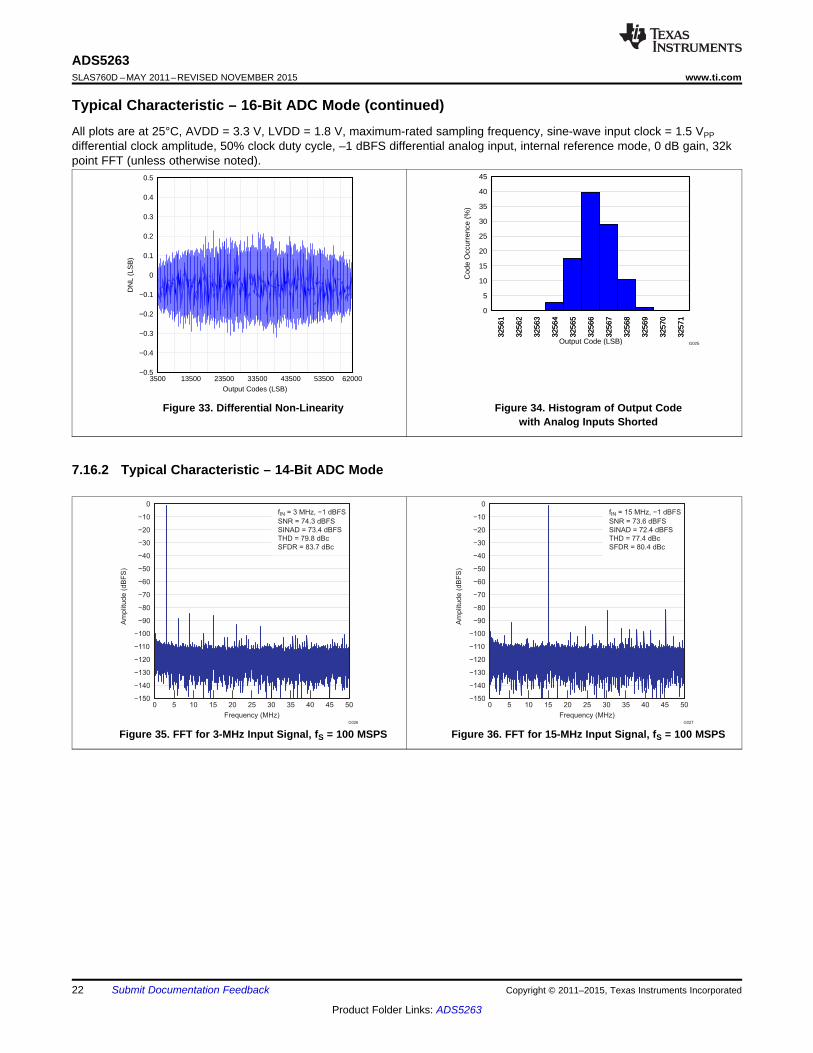
Typical Characteristic – 16-Bit ADC Mode (continued)All plots are at 25°C, AVDD = 3.3 V, LVDD = 1.8 V, maximum-rated sampling frequency, sine-wave input clock = 1.5 VPPdifferential clock amplitude, 50% clock duty cycle, –1 dBFS differential analog input, internal reference mode, 0 dB gain, 32kpoint FFT (unless otherwise noted).
Figure 33. Differential Non-Linearity Figure 34. Histogram of Output Codewith Analog Inputs Shorted
7.16.2 Typical Characteristic – 14-Bit ADC Mode
Figure 35. FFT for 3-MHz Input Signal, fS = 100 MSPS Figure 36. FFT for 15-MHz Input Signal, fS = 100 MSPS
22 Submit Documentation Feedback Copyright © 2011–2015, Texas Instruments Incorporated
Product Folder Links: ADS5263
40
60
80
100
120
140
160
180
200
220
240
10 20 30 40 50 60 70 80 90 100Sampling Frequency (MSPS)
Dig
ital P
ower
(m
W)
1Wire2Wire
40
60
80
100
120
140
160
180
200
10 20 30 40 50 60 70 80 90 100Sampling Frequency (MSPS)
Dig
ital P
ower
(m
W)
1Wire2Wire
−150
−140
−130
−120
−110
−100
−90
−80
−70
−60
−50
−40
−30
−20
−10
0
0 5 10 15 20 25 30 35 40 45 50
Frequency (MHz)
Am
plit
ud
e (
dB
FS
)
fIN = 65 MHz, −1 dBFS
SNR = 71.2 dBFS
SINA = 70.1 dBFS
THD = 75.2 dBc
SFDR= 76 dBc
G028
ADS5263www.ti.com SLAS760D –MAY 2011–REVISED NOVEMBER 2015
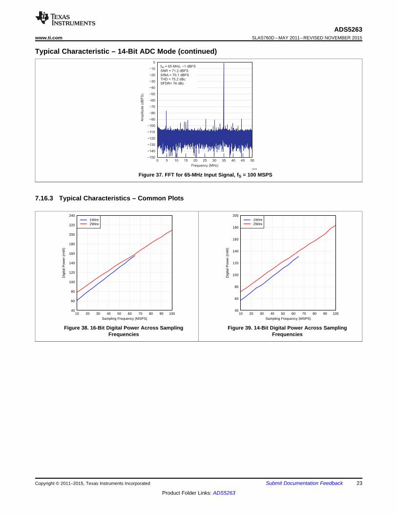
Typical Characteristic – 14-Bit ADC Mode (continued)
Figure 37. FFT for 65-MHz Input Signal, fS = 100 MSPS
7.16.3 Typical Characteristics – Common Plots
Figure 38. 16-Bit Digital Power Across Sampling Figure 39. 14-Bit Digital Power Across SamplingFrequencies Frequencies
Copyright © 2011–2015, Texas Instruments Incorporated Submit Documentation Feedback 23
Product Folder Links: ADS5263

79
81
81
81
83
83
83
83
85
85
85
85
85
Input Frequency, MHz
Sam
plin
g F
requency,
MS
PS
3 10 20 30 40 50 60 6520
30
40
50
60
70
80
90
100
79 80 81 82 83 84 85
71.5
72
72
72
72.5
72.5
72.5
73
73
73
73.5
73.5
73.5
74
74
74
74.5
74.5
74.5
Input Frequency, MHz
Sa
mp
ling
Fre
qu
en
cy,
MS
PS
3 10 20 30 40 50 60 6520
30
40
50
60
70
80
90
100
71.5 72 72.5 73 73.5 74 74.5
77
78
78
78
79
79
79
80
80
80
81
81
81
82
82
82
83
83
83
84
84
84
85
85
85
86
Input Frequency, MHz
Sa
mp
ling
Fre
qu
en
cy,
MS
PS
3 10 20 30 40 50 60 7020
30
40
50
60
70
80
90
100
77 78 79 80 81 82 83 84 85
76
76
76
78
78
78
80
80
80
80
82
82
82
8284
Input Frequency, MHz
Sa
mp
ling
Fre
qu
en
cy,
MS
PS
3 10 20 30 40 50 60 7020
30
40
50
60
70
80
90
100
75 76 77 78 79 80 81 82 83 84
ADS5263SLAS760D –MAY 2011–REVISED NOVEMBER 2015 www.ti.com
Typical Characteristics – Common Plots (continued)
Figure 40. SNR Contour Across Sampling and Input Figure 41. SFDR Contour Across Sampling and InputFrequencies, 16-Bit ADC Frequencies, 16-Bit ADC
Figure 42. SNR Contour Across Sampling and Input Figure 43. SFDR Contour Across Sampling and InputFrequencies, 14-Bit ADC Frequencies, 14-Bit ADC
24 Submit Documentation Feedback Copyright © 2011–2015, Texas Instruments Incorporated
Product Folder Links: ADS5263
ADS5263www.ti.com SLAS760D –MAY 2011–REVISED NOVEMBER 2015
8 Detailed Description
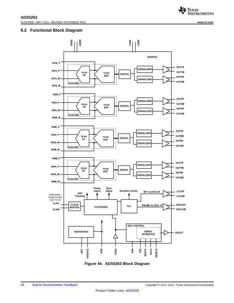
8.1 OverviewThe ADS5263 is a high-SNR 16-bit, quad-channel, 100-MSPS ADC using serial LVDS interface to reduce pinconnections from ADC to FPGA. For low power applications, the part can be progammed into 14-bit, Low-powermode saving 615 m-W at 100-MSPS
The ADS5263 has a digital processing block that integrates several commonly used digital functions, such asdigital gain (up to 12 dB). It includes a digital filter module that has built-in decimation filters (with low-pass, high-pass and band-pass characteristics). The decimation rate is also programmable (by 2, by 4, or by 8). This makesit very useful for narrow-band applications, where the filters can be used to improve SNR and knock-offharmonics, while at the same time reducing the output data rate.
The device includes an averaging mode where two channels (or even four channels) can be averaged to improveSNR. A very unique feature is the programmable mapper module that allows flexible mapping between the inputchannels and the LVDS output pins. This helps to greatly reduce the complexity of LVDS output routing and canpotentially result in cheaper system boards by reducing the number of PCB layers.
The data from each channel ADC is serialized and output on two pairs of LVDS output lines, along with a bitclock and a frame clock. Serial LVDS outputs reduce the number of interface lines. This, together with the low-power design, enables four channels to be packaged in a compact 9-mm × 9-mm QFN, allowing high systemintegration densities.
In order to ease interfacing to CCD sensors, a clamp function is integrated in the device. Using this feature, theanalog input pins can be clamped to an internal voltage, based on a SYNC signal. With this, the CCD sensoroutput can be easily ac-coupled to the ADS5263 analog inputs. The clamp feature and quad channels in acompact package make the ADS5263 attractive for industrial CCD imaging applications.
The device integrates an internal reference trimmed to accurately match across devices. Additionally, the devicesupports an external reference mode for applications that require very low temperature drift of reference. TheADS5263 is available in a non-magnetic QFN package that does not create any MRI signature. The device isspecified over the full industrial temperature range.
Copyright © 2011–2015, Texas Instruments Incorporated Submit Documentation Feedback 25
Product Folder Links: ADS5263
REFERENCE
DIGITAL
SERIALINTERFACE
IN1A_P
IN1A_M
CLKP
CLKM
VC
M
SC
LK
CS
Z
SD
AT
A
RE
SE
TZ
LCLKP
LCLKM
ADS5263
14 bitADC
ADCLKP
ADCLKM
SY
NC
INT
/EX
TZ
PLL
BIT CLOCK, 8X
FRAME CLOCK, 1X
OUT1P
OUT1M
OUT2P
OUT2M
AV
DD
AG
ND
LV
DD
LG
ND
PD
N
16 bitFE
16 bit ADC
SERIALIZER
SERIALIZER
IN1B_P
IN1B_M
DIGITAL
IN2A_P
IN2A_M
14 bitADC
OUT3P
OUT3M
OUT4P
OUT4M
16 bitFE
16 bit ADC
SERIALIZER
SERIALIZER
IN2B_P
IN2B_M
DIGITAL
IN3A_P
IN3A_M
14 bitADC
OUT5P
OUT5M
OUT6P
OUT6M
16 bitFE
16 bit ADC
SERIALIZER
SERIALIZER
IN3B_P
IN3B_M
DIGITAL
IN4A_P
IN4A_M
14 bitADC
OUT7P
OUT7M
OUT8P
OUT8M
16 bitFE
16 bit ADC
SERIALIZER
SERIALIZER
IN4B_P
IN4B_M
CLOCKBUFFER CLOCKGEN
ADC CONTROL
ISE
T
SDOUT
Clampsignal
ADCClocking
Serializer clocksSyncsignal
Differential /Single-EndedInput Clock
ADS5263SLAS760D –MAY 2011–REVISED NOVEMBER 2015 www.ti.com
8.2 Functional Block Diagram
Figure 44. ADS5263 Block Diagram
26 Submit Documentation Feedback Copyright © 2011–2015, Texas Instruments Incorporated
Product Folder Links: ADS5263
24-tap filter(Even Tap)
24-tap filter(Even Tap)
Decimation
by 2 or
by 4
GAIN
(0 to 12 dB ,
1 dB steps )
DIGITAL PROCESSING BLOCK for CHANNEL 1
Test Patterns-
Ramp
MAPPER
MULTIPLEXER8 : 8
LVDS OUTPUTS
16-BITADC
ADS5263
Average of 2channels
Average of 4channels
Channel 1 ADC Data
23-tap filter(Odd Tap)
Built-in Coefficients
Decimation
by 2 or
by 4 or
by 8
Custom Coefficients
Serializer
Wire 1
Serializer
Wire 2
Channel 1
Serializer
Wire 1
Serializer
Wire 2
Channel 2
Serializer
Wire 1
Serializer
Wire 2
Channel 3
Serializer
Wire 1
Serializer
Wire 2
Channel 4
OUT 1A
OUT 1B
OUT 2A
OUT 2B
OUT 3A
OUT 3B
OUT 4A
OUT 4B
12-tap filter
Channel 2 ADC DataChannel 3 ADC DataChannel 4 ADC Data
23-tap filter(Odd Tap)
ADS5263www.ti.com SLAS760D –MAY 2011–REVISED NOVEMBER 2015
8.3 Feature Description
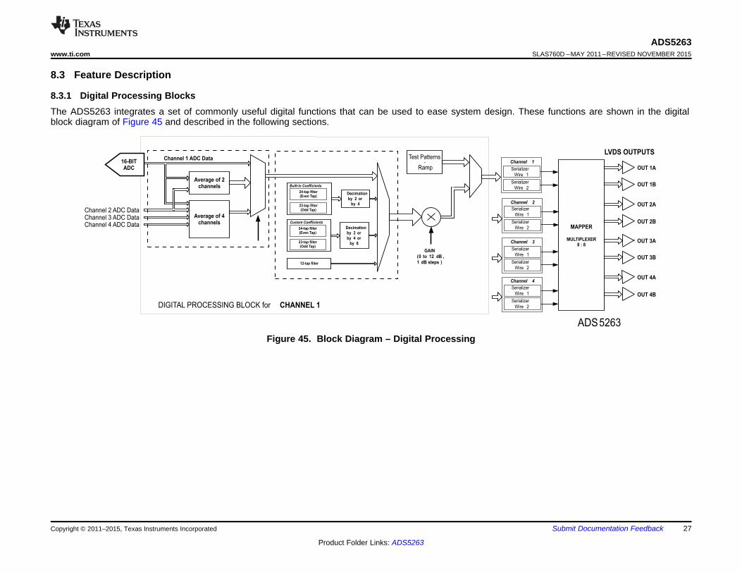
8.3.1 Digital Processing BlocksThe ADS5263 integrates a set of commonly useful digital functions that can be used to ease system design. These functions are shown in the digitalblock diagram of Figure 45 and described in the following sections.
Figure 45. Block Diagram – Digital Processing
Copyright © 2011–2015, Texas Instruments Incorporated Submit Documentation Feedback 27
Product Folder Links: ADS5263

ADS5263SLAS760D –MAY 2011–REVISED NOVEMBER 2015 www.ti.com
8.3.2 Digital GainADS5263 includes programmable digital gain settings from 0 dB to 12 dB in steps of 1 dB. The benefit of digitalgain is to get improved SFDR performance. The SFDR improvement is achieved at the expense of SNR; foreach gain setting, the SNR degrades by about 1 dB. So, the gain can be used to trade off between SFDR andSNR.
For each gain setting, the analog supported input full-scale range scales proportionally, as shown in Table 1. Thefull-scale range depends on the ADC mode used (16-bit or 14-bit).
After a reset, the device comes up in the 0-dB gain mode. To use other gain settings, program the <GAIN CH x>register bits.
Table 1. Analog Full-Scale Range Across Gains16-BIT ADC MODE 14-BIT ADC MODEDIGITAL GAIN,
dB ANALOG FULL-SCALE INPUT, Vpp ANALOG FULL-SCALE INPUT, Vpp0 4.00 21 3.57 1.782 3.18 1.593 2.83 1.424 2.52 1.265 2.25 1.126 2.00 1.007 1.79 0.898 1.59 0.809 1.42 0.7110 1.26 0.6311 1.13 0.5612 1.00 0.50
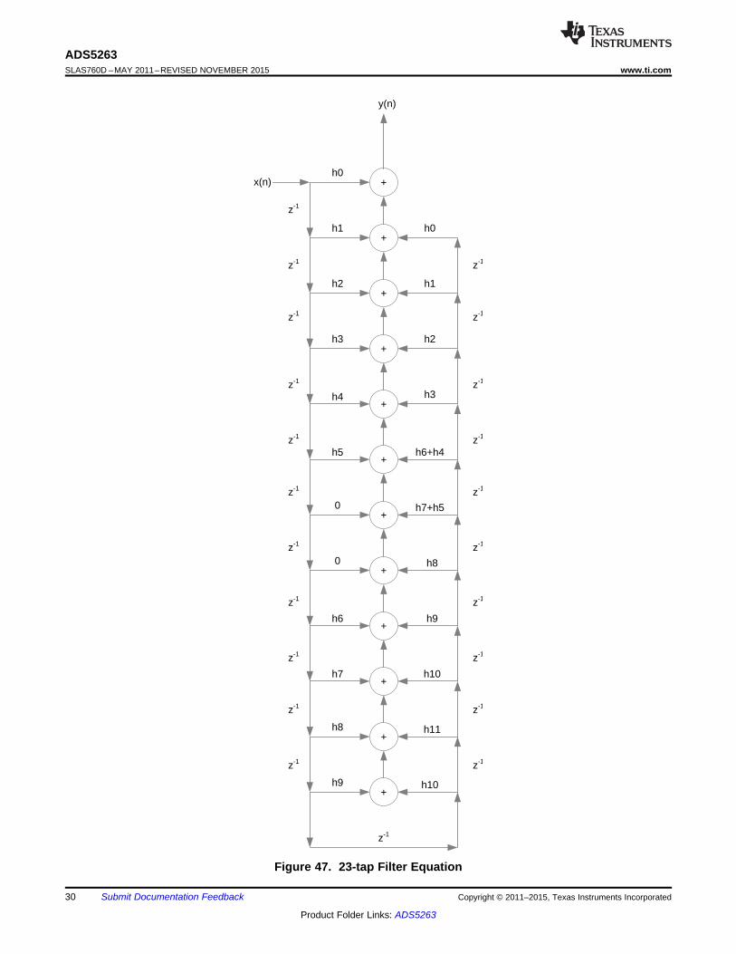
8.3.3 Digital FilterThe digital processing block includes the option to filter and decimate the ADC data outputs digitally. Variousfilters and decimation rates are supported – decimation rates of 2, 4, and 8 and low-pass, high-pass, and band-pass filters are available. The filters are internally implemented as a 24-tap asymmetric FIR (even-tap) using pre-defined coefficients following the equation which is described in Figure 46.
Alternatively, some of the filters can be configured as a 23-tap asymmetric FIR (or odd-tap filters) following theequation which is described in Figure 47.
28 Submit Documentation Feedback Copyright © 2011–2015, Texas Instruments Incorporated
Product Folder Links: ADS5263

+
+
+
+
+
+
+
+
+
+
+
+
h0 h0
h1 h1
h2 h2
h3 h3
h4 h6+h4
h5 h7+h5
h6
h11
h7
h10
h8
h8
h9
h9
0
h10
0
h11
z-1
z-1
z-1
z-1
z-1
z-1
z-1
z-1
z-1
z-1
z-1
z-1
z-1
z-1
z-1
z-1
z-1
z-1
z-1
z-1
z-1
z-1
z-1
x(n)
y(n)
ADS5263www.ti.com SLAS760D –MAY 2011–REVISED NOVEMBER 2015
Figure 46. 24-tap Filter EquationCopyright © 2011–2015, Texas Instruments Incorporated Submit Documentation Feedback 29
Product Folder Links: ADS5263
+
+
+
+
+
+
+
+
+
+
+
+
h0
h0h1
h1h2
h2h3
h3h4
h6+h4h5
h7+h5
h6
h7
h10
h8
h8
h9
h9
0
h10
0
h11
z-1
z-1
z-1
z-1
z-1
z-1
z-1
z-1
z-1
z-1
z-1
z-1
z-1
z-1
z-1
z-1
z-1
z-1
z-1
z-1
z-1
z-1
x(n)
y(n)
ADS5263SLAS760D –MAY 2011–REVISED NOVEMBER 2015 www.ti.com
Figure 47. 23-tap Filter Equation
30 Submit Documentation Feedback Copyright © 2011–2015, Texas Instruments Incorporated
Product Folder Links: ADS5263

−80
−70
−60
−50
−40
−30
−20
−10
0
10
20
30
0 0.1 0.2 0.3 0.4 0.5Normalized Frequency (Fin/Fs)
Nor
mal
ized
Am
plitu
de (
dB)
HighpassLow pass
−80
−70
−60
−50
−40
−30
−20
−10
0
10
20
30
40
50
0 0.1 0.2 0.3 0.4 0.5Normalized Frequency (Fin/Fs)
Nor
mal
ized
Am
plitu
de (
dB)
Low−passBand−pass1Band−pass2High−pass
ADS5263www.ti.com SLAS760D –MAY 2011–REVISED NOVEMBER 2015
In the equations,
h0, h1 …h11 are 12-bit signed 2s complement representation of the coefficients (-2048 to +2047)
x(n) is the input data sequence to the filter
y(n) is the filter output sequence
Details of the registers used for configuring the digital filters are show in Table 2 and Table 3.
Table 2. Digital Filter RegistersBIT NAME DESCRIPTION
ADDR: 2E, 2F, 30, 31 Default = 0D9-D7 FILTER TYPE CHn<2:0> Selects low-pass, high-pass or band-pass filtersD6-D4 DEC by RATE CHn<2:0> Selects the decimation rate
D2 ODD TAP CHn Even tap or odd tapD0 USE FILTER CHn Enables the filter
ADDR: 38, Default = 0D1-D0 OUTPUT RATE<1:0> Select output data rate depending on the type of filter
ADDR: 29, Default = 0D1 EN DIG FILTER Enables digital filter – global control
See Table 3 for choosing the right combination of decimation rate and filter types.
Table 3. Digital Filters<SEL <USE <EN<OUTPUT DEC by <FILTERDECIMATION TYPE OF FILTER ODD FILTER CUSTOM <EN DIG FILTER>RATE> RATE CHx> TYPE CHx> TAP> CHx> FILT>
Built-in low-pass odd-tap filter (pass band = 0 to fS/4) 001 000 000 1 1 0 1Decimate by 2
Built-in high-pass odd-tap filter (pass band = 0 to fS/4) 001 000 001 1 1 0 1
Built-in low-pass even-tap filter (pass band = 0 to fS/8) 010 001 010 0 1 0 1
Built-in first band pass even tap filter(pass band = fS/8 010 001 011 0 1 0 1to fS/4)Decimate by 4 Built-in second band pass even tap filter(pass band = 010 001 100 0 1 0 1fS/4 to 3 fS/8)
Built-in high pass odd tap filter (pass band = 3 fS/8 to 010 001 101 1 1 0 1fS/2)
Decimate by 2 Custom filter (user programmablecoefficients) 001 000 000 0 or 1 1 1 1
Decimate by 4 Custom filter (user programmablecoefficients) 010 001 000 0 or 1 1 1 1
Decimate by 8 Custom filter (user programmablecoefficients) 011 100 000 0 or 1 1 1 1
12-tap filterwithout Custom filter (user programmablecoefficients) 000 011 000 0 1 1 1decimation
Figure 48. Filter Response – Decimate by 2 Figure 49. Filter Response – Decimate by 4
Copyright © 2011–2015, Texas Instruments Incorporated Submit Documentation Feedback 31
Product Folder Links: ADS5263
ADS5263SLAS760D –MAY 2011–REVISED NOVEMBER 2015 www.ti.com
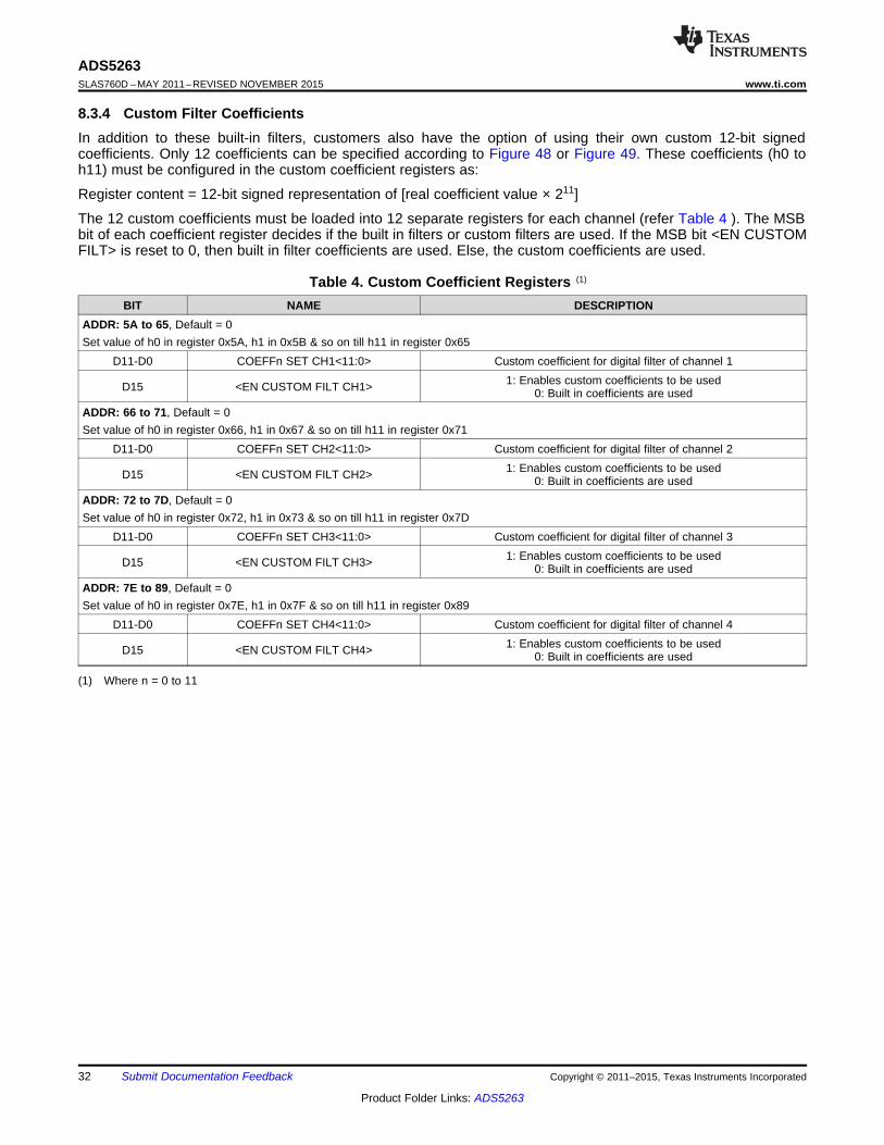
8.3.4 Custom Filter CoefficientsIn addition to these built-in filters, customers also have the option of using their own custom 12-bit signedcoefficients. Only 12 coefficients can be specified according to Figure 48 or Figure 49. These coefficients (h0 toh11) must be configured in the custom coefficient registers as:
Register content = 12-bit signed representation of [real coefficient value × 211]
The 12 custom coefficients must be loaded into 12 separate registers for each channel (refer Table 4 ). The MSBbit of each coefficient register decides if the built in filters or custom filters are used. If the MSB bit <EN CUSTOMFILT> is reset to 0, then built in filter coefficients are used. Else, the custom coefficients are used.
Table 4. Custom Coefficient Registers (1)
BIT NAME DESCRIPTIONADDR: 5A to 65, Default = 0Set value of h0 in register 0x5A, h1 in 0x5B & so on till h11 in register 0x65
D11-D0 COEFFn SET CH1<11:0> Custom coefficient for digital filter of channel 11: Enables custom coefficients to be usedD15 <EN CUSTOM FILT CH1> 0: Built in coefficients are used
ADDR: 66 to 71, Default = 0Set value of h0 in register 0x66, h1 in 0x67 & so on till h11 in register 0x71
D11-D0 COEFFn SET CH2<11:0> Custom coefficient for digital filter of channel 21: Enables custom coefficients to be usedD15 <EN CUSTOM FILT CH2> 0: Built in coefficients are used
ADDR: 72 to 7D, Default = 0Set value of h0 in register 0x72, h1 in 0x73 & so on till h11 in register 0x7D
D11-D0 COEFFn SET CH3<11:0> Custom coefficient for digital filter of channel 31: Enables custom coefficients to be usedD15 <EN CUSTOM FILT CH3> 0: Built in coefficients are used
ADDR: 7E to 89, Default = 0Set value of h0 in register 0x7E, h1 in 0x7F & so on till h11 in register 0x89
D11-D0 COEFFn SET CH4<11:0> Custom coefficient for digital filter of channel 41: Enables custom coefficients to be usedD15 <EN CUSTOM FILT CH4> 0: Built in coefficients are used
(1) Where n = 0 to 11
32 Submit Documentation Feedback Copyright © 2011–2015, Texas Instruments Incorporated
Product Folder Links: ADS5263
+
+
+
+
+
+
h6
h7
h8
h9
h10
h11
z-1
z-1
z-1
z-1
z-1
z-1
z-1
z-1
z-1
z-1
z-1
x(n)h6
h7
h8
h9
h10
h11
y(n)
ADS5263www.ti.com SLAS760D –MAY 2011–REVISED NOVEMBER 2015
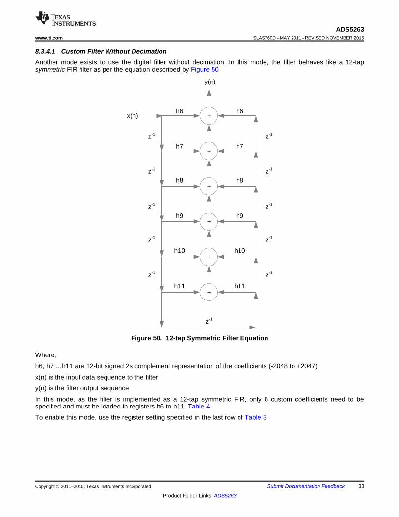
8.3.4.1 Custom Filter Without DecimationAnother mode exists to use the digital filter without decimation. In this mode, the filter behaves like a 12-tapsymmetric FIR filter as per the equation described by Figure 50
Figure 50. 12-tap Symmetric Filter Equation
Where,
h6, h7 …h11 are 12-bit signed 2s complement representation of the coefficients (-2048 to +2047)
x(n) is the input data sequence to the filter
y(n) is the filter output sequence
In this mode, as the filter is implemented as a 12-tap symmetric FIR, only 6 custom coefficients need to bespecified and must be loaded in registers h6 to h11. Table 4
To enable this mode, use the register setting specified in the last row of Table 3
Copyright © 2011–2015, Texas Instruments Incorporated Submit Documentation Feedback 33
Product Folder Links: ADS5263
ADS5263SLAS760D –MAY 2011–REVISED NOVEMBER 2015 www.ti.com
8.3.5 Digital AveragingThe ADS5263 includes an averaging function where the ADC digital data from two (or four) channels can beaveraged. The averaged data is output on specific LVDS channels. Table 5 shows the combinations of the inputchannels that can be averaged and the LVDS channels on which averaged data is available
Table 5. Using Channel AveragingOutput on Which Averaged Data IsAveraged Channels Register SettingsAvailable
Channel 1, Channel 2 OUT1A, OUT1B Set <AVG OUT 1> = 10 and <EN AVG GLO> = 1Channel 1, Channel 2 OUT3A, OUT3B Set <AVG OUT 3> = 11 and <EN AVG GLO> = 1Channel 3, Channel 4 OUT4A, OUT4B Set <AVG OUT 4> = 10 and <EN AVG GLO> = 1Channel 3, Channel 4 OUT2A, OUT2B Set <AVG OUT 2> = 11 and <EN AVG GLO> = 1
Channel 1, Channel 2, Channel 3, Channel 4 OUT1A, OUT1B Set <AVG OUT 1> = 11 and <EN AVG GLO> = 1Channel 1, Channel 2, Channel 3, Channel 4 OUT1A, OUT1B Set <AVG OUT 4> = 11 and <EN AVG GLO> = 1
8.3.6 Performance with Digital Processing BlocksThe ADS5263 provides very high SNR along with high sampling rates. In applications where even higher SNRperformance is desired, digital processing blocks such as averaging and decimation filters can be usedadvantageously to achieve this. Table 6 shows the improvement in SNR that can be achieved compared to thedefault value, using these modes.
Table 6. SNR Improvement Using Digital Processing (1)
MODE TYPICAL SNR, dBFS TYPICAL IMPROVEMENT in SNR, dBDefault 84.5With decimation-by-2 filter enabled 86.7 2.2With decimation-by-4 filter enabled 87.7 3.2With decimation-by-8 filter enabled 88.6 4.1With two channels averaged and decimation-by-8 filter enabled 91.3 6.8With four channels averaged 89.6 5.1With four channels averaged and decimation-by-8 filter enabled 93 8.5
(1) Custom coefficients used for decimation-by-8 filter.
8.3.6.1 18-Bit Data Output with Digital ProcessingAs shown in Table 6, very high SNR can be achieved using the digital blocks. Now, the overall SNR is limited bythe quantization noise of the 16-bit output data. (16-bit quantization SNR = 6n + 1.76 = 16 × 6 + 1.76 = 97.76dBFS.) To overcome this, the digital processing blocks (averaging and digital filters) automatically output 18-bitdata. With the two additional bits, the quantization SNR improves by 12 dB and no longer limits the maximumSNR that can be achieved using the ADS5263. For example, with four channels averaged and the decimation-by-8 filter, the typical SNR improves to about 94.5 dBFS using 18-bit data (an improvement of 1.5 dB over theSNR with 16-bit data).
The 18-bit data can be output using the special 18× serialization mode (see Output LVDS Interface). Note thatthe user can choose either the default 16× serialization (which takes the upper 16 bits of the 18-bit data) or the18× serialization mode (that outputs all 18 bits).
8.3.7 Flexible Mapping o Channel Data to LVDS OutputsADS5263 has a mapping function by the use of which the digital data for any channel can be routed to any LVDSoutput. So, as an example, in the 1-wire interface, the channel-1 ADC output can be output either on OUT1 pinsor on OUT2 or OUT3 or OUT4 pins.
This flexibility in mapping simplifies board designs by avoiding complex routing that would be caused by a rigidmapping of input channels and output pins. This can also lead to potential saving in PCB layers and hence cost.The mapping is programmable using the register bits <MAP_Ch1234_OUTn> as shown in Figure 51 andFigure 52.
34 Submit Documentation Feedback Copyright © 2011–2015, Texas Instruments Incorporated
Product Folder Links: ADS5263

Channel 1 Data[15:0]
Set MAP_Ch1234_OUTn<3:0> = 0000
Channel 2 Data[15:0]
Set MAP_Ch1234_OUTn<3:0> = 0010
Channel 3 Data[15:0]
Set MAP_Ch1234_OUTn<3:0> = 0100
Channel 4 Data[15:0]
Set MAP_Ch1234_OUTn<3:0> = 0110
Power down LVDS buffer OUTn
Set MAP_Ch1234_OUTn<3:0> = 1xxx
LVDS Output Buffer, OUTn
PDN
IN OUT
ADS5263
n = 1A, 1B, 2A, 2B, 3A, 3B, 4A, 4B
Channel 1 MSB Data[15:8]
Set MAP_Ch1234_OUTn<3:0> = 0000
Channel 1 LSB Data[7:0]
Set MAP_Ch1234_OUTn<3:0> = 0001
Channel 2 MSB Data[15:8]
Set MAP_Ch1234_OUTn<3:0> = 0010
Channel 2 LSB Data[7:0]
Set MAP_Ch1234_OUTn<3:0> = 0011
Channel 3 MSB Data[15:8]
Set MAP_Ch1234_OUTn<3:0> = 0100
Channel 3 LSB Data[7:0]
Set MAP_Ch1234_OUTn<3:0> = 0101
Channel 4 MSB Data[15:8]
Set MAP_Ch1234_OUTn<3:0> = 0110
Channel 4 LSB Data[7:0]
Set MAP_Ch1234_OUTn<3:0> = 0111
Power down LVDS buffer OUTn
Set MAP_Ch1234_OUTn<3:0> = 1xxx
LVDS Output Buffer, OUTn
PDN
IN OUT
ADS5263
n = 1A, 1B, 2A, 2B, 3A, 3B, 4A, 4B
ADS5263www.ti.com SLAS760D –MAY 2011–REVISED NOVEMBER 2015
Figure 51. Mapping in 2-Wire Interface
Figure 52. Mapping in 1-Wire Interface
Copyright © 2011–2015, Texas Instruments Incorporated Submit Documentation Feedback 35
Product Folder Links: ADS5263

ADS5263SLAS760D –MAY 2011–REVISED NOVEMBER 2015 www.ti.com
8.3.8 Output LVDS InterfaceThe ADS5263 offers several flexible output options, making it easy to interface to an ASIC or an FPGA. Each ofthese options can be easily programmed using the serial interface. A summary of all the options is presented inTable 7, along with the default values after power up and reset. Following this, each option is described in detail.
The output interface options are:1. 1-wire, 16× serialization with DDR bit clock and 1× frame clock
– The 16-bit ADC data is serialized and output over one LVDS pair per channel together with an 8× bit clock and 1×frame clock. The output data rate is 16× sample rate; hence, it is suited for low sample rates, typically up to 50MSPS.
2. 2-wire, 8× serialization with DDR bit clock and 0.5× frame clock (16 bit ADC mode, Figure 54 and Figure 55)– Here, the 16 bit ADC data is serialized and output over two LVDS pairs per channel. The output data rate is 8x
sample rate, with a 4x bit clock and 0.5x frame clock.Because the output data rate is half compared to the 1-wire case, this interface can be used up to the maximumsample rate of the device.
3. 2-wire, 8× serialization with DDR bit clock and 0.5× frame clock (14-bit ADC mode)– Here, the 14-bit ADC data is padded with two zero bits. The combined 16-bit data is then serialized and output over
two LVDS pairs per channel. The output data rate is 8× sample rate, with a 4× bit clock and 0.5× frame clockBecause the output data rate is half compared to the 1-wire case, this interface can be used up to the maximumsample rate of the device.
4. 1-wire, 14× serialization with DDR bit clock and 1× frame clock (14-bit ADC mode)– The 14-bit ADC data is serialized and output over one LVDS pair per channel together with a 7× bit clock and 1×
frame clock. The output data rate is 14× sample rate; hence, it is suited for low sample rates, typically up to 50MSPS.
5. 2-wire, 7× serialization with DDR bit clock and 0.5× frame clock (14-bit ADC mode, Figure 57 and Figure 58)– Here, the 14-bit ADC data is serialized and output over two LVDS pairs per channel. The output data rate is 7×
sample rate, with a 3.5× bit clock and 0.5× frame clock. Because the output data rate is half compared to the 1-wirecase, this interface can be used up to the maximum sample rate of the device.
6. 1-wire, 18× serialization with DDR bit clock and 1× frame clock – Here, the 18-bit data from the digital processing block isserialized and output over one LVDS pair per channel, together with a 9× bit clock and 1x frame clock. The output datarate is 18× sample rate; hence, it is suited for low sample rates, typically up to 40 MSPS. This interface is primarilyintended to be used when the averaging and digital filters are enabled.
Table 7. Summary of Output Interface OptionsAVAILABLE DEFAULT
INFEATURE OPTIONS AFTER POWER BRIEF DESCRIPTIONUP AND RESET1 wire 2 wire
Wire interface 1 wire and 1 wire 1 wire – ADC data is sent serially over one pair of LVDS pins2 wire – ADC data is split and sent serially over two pairs of2 wireLVDS pins
Serialization factor 16× X X 16× For 16-bit ADC modeCan also be used with 14-bit ADC mode – the 14-bit ADC datais padded with two zeros and the combined 16-bit data isserialized.
18× X 18-bit data is available when 16-bit ADC mode is used withaveraging and decimation filters enabled.
14× X X For 14-bit ADC mode onlyDDR bit-clock 8× X 8× 16× serializationfrequency 4× X 16× serialization
Only with 2-wire interface9× X 18× serialization7× X 14× serialization
3.5× X 14× serializationOnly with 2-wire interface
36 Submit Documentation Feedback Copyright © 2011–2015, Texas Instruments Incorporated
Product Folder Links: ADS5263
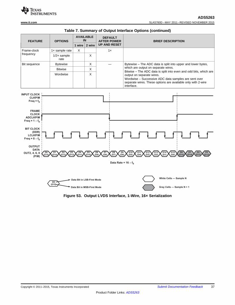
OUTPUT
DATA
OUT2, 4, 6, 8
(P/M)
FRAME
CLOCK
ADCLKP/M
LCLKP/M
BIT CLOCK
(DDR)
INPUT CLOCK
CLKP/M
Freq = fS
Freq = 1 f´ S
Freq = 8 f´ S
Data Bit in LSB-First Mode
Data Bit in MSB-First Mode
Data Rate = 16 ´ fS
White Cells — Sample N
Gray Cells — Sample N + 1
D0(D15)
D0(D15)
D0(D15)
D1(D14)
D1(D14)
D2(D13)
D2(D13)
D3(D12)
D3(D12)
D4(D11)
D5(D10)
D6(D9)
D7(D8)
D8(D7)
D9(D6)
D10(D5)
D11(D4)
D12(D3)
D13(D2)
D14(D1)
D15(D0)
ADS5263www.ti.com SLAS760D –MAY 2011–REVISED NOVEMBER 2015
Table 7. Summary of Output Interface Options (continued)AVAILABLE DEFAULT
INFEATURE OPTIONS AFTER POWER BRIEF DESCRIPTIONUP AND RESET1 wire 2 wire
Frame-clock 1× sample rate X 1×frequency 1/2× sample X
rateBit sequence Bytewise X — Bytewise – The ADC data is split into upper and lower bytes,
which are output on separate wires.Bitwise XBitwise – The ADC data is split into even and odd bits, which are
Wordwise X output on separate wires.Wordwise – Successive ADC data samples are sent overseparate wires. These options are available only with 2-wireinterface.
Figure 53. Output LVDS Interface, 1-Wire, 16× Serialization
Copyright © 2011–2015, Texas Instruments Incorporated Submit Documentation Feedback 37
Product Folder Links: ADS5263
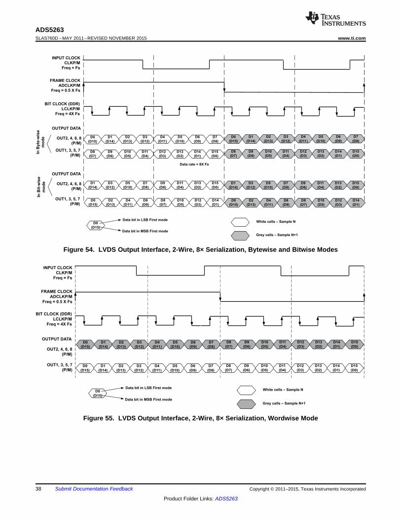
Data bit in LSB First mode
Data bit in MSB First mode
D0
(D15)
D0
(D15)
D1
(D14)
D2
(D13)
D3
(D12)
D4
(D11)
D5
(D10)
D6
(D9)
D7
(D8)
D8
(D7)
D9
(D6)
D10
(D5)
D11
(D4)
D12
(D3)
D13
(D2)
D14
(D1)
D15
(D0)
White cells – Sample N
Grey cells – Sample N+1
D0
(D15)
D1
(D14)
D2
(D13)
D3
(D12)
D4
(D11)
D5
(D10)
D6
(D9)
D7
(D8)
D8
(D7)
D9
(D6)
D10
(D5)
D11
(D4)
D12
(D3)
D13
(D2)
D14
(D1)
D15
(D0)
OUTPUT DATA
OUT2, 4, 6, 8
(P/M)
FRAME CLOCK
ADCLKP/M
Freq = 0.5 X Fs
BIT CLOCK (DDR)
LCLKP/M
Freq = 4X Fs
INPUT CLOCK
CLKP/M
Freq = Fs
OUT1, 3, 5, 7
(P/M)
OUTPUT DATA
OUT2, 4, 6, 8
(P/M)
FRAME CLOCK
ADCLKP/M
Freq = 0.5 X Fs
D0
(D15)
D1
(D14)
D2
(D13)
D3
(D12)
D4
(D11)
D5
(D10)
D6
(D9)
D7
(D8)
D8
(D7)
D9
(D6)
D10
(D5)
D11
(D4)
D12
(D3)
D13
(D2)
D14
(D1)
D15
(D0)
BIT CLOCK (DDR)
LCLKP/M
Freq = 4X Fs
D1
(D14)
D3
(D12)
D5
(D10)
D7
(D8)
D9
(D6)
D11
(D4)
D13
(D2)
D15
(D0)
D0
(D15)
D2
(D13)
D4
(D11)
D6
(D9)
D8
(D7)
D10
(D5)
D12
(D3)
D14
(D1)
InB
yte
-wis
e
mo
de
InB
it-w
ise
mo
de
INPUT CLOCK
CLKP/M
Freq = Fs
Data bit in LSB First mode
Data bit in MSB First mode
D0
(D15)
OUT1, 3, 5, 7
(P/M)
Data rate = 8X Fs
White cells – Sample N
Grey cells – Sample N+1
OUTPUT DATA
OUT2, 4, 6, 8
(P/M)
OUT1, 3, 5, 7
(P/M)
D0
(D15)
D1
(D14)
D2
(D13)
D3
(D12)
D4
(D11)
D5
(D10)
D6
(D9)
D7
(D8)
D8
(D7)
D9
(D6)
D10
(D5)
D11
(D4)
D12
(D3)
D13
(D2)
D14
(D1)
D15
(D0)
D1
(D14)
D3
(D12)
D5
(D10)
D7
(D8)
D9
(D6)
D11
(D4)
D13
(D2)
D15
(D0)
D0
(D15)
D2
(D13)
D4
(D11)
D6
(D9)
D8
(D7)
D10
(D5)
D12
(D3)
D14
(D1)
ADS5263SLAS760D –MAY 2011–REVISED NOVEMBER 2015 www.ti.com
Figure 54. LVDS Output Interface, 2-Wire, 8× Serialization, Bytewise and Bitwise Modes
Figure 55. LVDS Output Interface, 2-Wire, 8× Serialization, Wordwise Mode
38 Submit Documentation Feedback Copyright © 2011–2015, Texas Instruments Incorporated
Product Folder Links: ADS5263

!
"
"
#$
$%
&'&#('()#*(+',-
&'&#('()#* (+',-
!
&'&&'
./('011+2 &341%
56011+2 &341%7
!
OUTPUT
DATA
OUT2, 4, 6, 8
(P/M)
FRAME
CLOCK
ADCLKP/M
Freq = 1X Fs
BIT CLOCK
(DDR)
LCLKP/M
Freq = 9X Fs
INPUT CLOCK
CLKP/M
Freq = Fs
Data bit in LSB First mode
Data bit in MSB First mode
D0
(D17)
Data rate = 18X Fs
White cells – Sample N
Grey cells – Sample N+1
D1(D16)
D2(D15)
D3(D14)
D4(D13)
D5(D12)
D6(D11)
D7(D10)
D8(D9)
D0(D17)
D9(D8)
D10(D7)
D11(D6)
D12(D5)
D13(D4)
D14(D3)
D15(D2)
D1(D16)
D16(D1)
D17(D0)
D0(D17)
D2(D15)
D3(D14)
D4(D13)
ADS5263www.ti.com SLAS760D –MAY 2011–REVISED NOVEMBER 2015
Figure 56. LVDS Output Interface, 1-Wire, 18× Serialization
Figure 57. LVDS Output Interface, 1-Wire, 14× Serialization
Copyright © 2011–2015, Texas Instruments Incorporated Submit Documentation Feedback 39
Product Folder Links: ADS5263
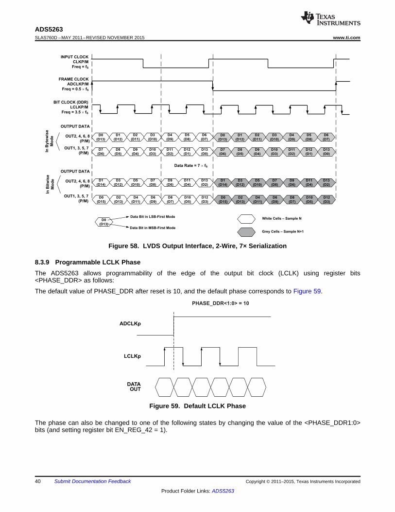
ADCLKp
LCLKp
DATAOUT
PHASE_DDR<1:0> = 10
OUTPUT DATA
OUT2, 4, 6, 8
(P/M)
FRAME CLOCK
ADCLKP/M
Freq = 0.5 ´ fS
D0
(D13)
D1
(D12)
D2
(D11)
D3
(D10)
D4
(D9)
D5
(D8)
D6
(D7)
D7
(D6)
D8
(D5)
D9
(D4)
D10
(D3)
D11
(D2)
D12
(D1)
D13
(D0)
BIT CLOCK (DDR)
LCLKP/M
Freq = 3.5 ´ fS
D1
(D14)
D3
(D12)
D5
(D10)
D7
(D8)
D9
(D6)
D11
(D4)
D13
(D2)
D0
(D15)
D2
(D13)
D4
(D11)
D6
(D9)
D8
(D7)
D10
(D5)
D12
(D3)
InB
yte
wis
e
Mo
de
InB
itw
ise
Mo
de
INPUT CLOCK
CLKP/M
Freq = fS
Data Bit in LSB-First Mode
Data Bit in MSB-First Mode
D0
(D13)
OUT1, 3, 5, 7
(P/M)
Data Rate = 7 ´ fS
White Cells – Sample N
Grey Cells – Sample N+1
OUTPUT DATA
OUT2, 4, 6, 8
(P/M)
OUT1, 3, 5, 7
(P/M)
D1
(D14)
D3
(D12)
D5
(D10)
D7
(D8)
D9
(D6)
D11
(D4)
D13
(D2)
D0
(D15)
D2
(D13)
D4
(D11)
D6
(D9)
D8
(D7)
D10
(D5)
D12
(D3)
D0
(D13)
D1
(D12)
D2
(D11)
D3
(D10)
D4
(D9)
D5
(D8)
D6
(D7)
D7
(D6)
D8
(D5)
D9
(D4)
D10
(D3)
D11
(D2)
D12
(D1)
D13
(D0)
ADS5263SLAS760D –MAY 2011–REVISED NOVEMBER 2015 www.ti.com
Figure 58. LVDS Output Interface, 2-Wire, 7× Serialization
8.3.9 Programmable LCLK PhaseThe ADS5263 allows programmability of the edge of the output bit clock (LCLK) using register bits<PHASE_DDR> as follows:
The default value of PHASE_DDR after reset is 10, and the default phase corresponds to Figure 59.
Figure 59. Default LCLK Phase
The phase can also be changed to one of the following states by changing the value of the <PHASE_DDR1:0>bits (and setting register bit EN_REG_42 = 1).
40 Submit Documentation Feedback Copyright © 2011–2015, Texas Instruments Incorporated
Product Folder Links: ADS5263

ADCLKp
LCLKp
DATA
OUT
ADCLKp
LCLKp
DATA
OUT
ADCLKp
LCLKp
DATA
OUT
ADCLKp
LCLKp
DATA
OUT
PHASE_DDR<1:0> = 10PHASE_DDR<1:0> = 00
PHASE_DDR<1:0> = 11PHASE_DDR<1:0> = 01
ADS5263www.ti.com SLAS760D –MAY 2011–REVISED NOVEMBER 2015
Figure 60. Programmable LCLK Phases
8.4 Device Functional Modes
8.4.1 Device ConfigurationADS5263 has several modes that can be configured using a serial programming interface, as described below.In addition, the device has dedicated parallel pins for controlling common functions such as power down andinternal or external reference selection.
Table 8. PDN CONTROL PINSTATE OF REGISTER BITVOLTAGE APPLIED ON PDN DESCRIPTION<CONFIG PDN pin>
0 V X (don't care) Normal operation0 Device enters global power-down mode
Logic HIGH1 Device enters standby mode
Table 9. INT/EXT CONTROL PINVOLTAGE APPLIED ON INT/EXT DESCRIPTION
0 V External reference mode. Apply voltage on VCM pin to set the references for ADC operation.Logic HIGH Internal reference
Copyright © 2011–2015, Texas Instruments Incorporated Submit Documentation Feedback 41
Product Folder Links: ADS5263

0 0 0 0 0 0 0 1 0 0 0 0 0 0 0 0SDATA
SCLK
CSZ
SDOUT
0 0 0 0 0 0 0 1
A) Enable Serial Readout (<READOUT> = 1)
REGISTER ADDRESS (A7:A0) = 0x01 REGISTER DATA (D15:D0) = 0x0001
Pin SDOUT is tri-stated
Pin SDOUT BecomesActive and Forces Low
SDATA
SCLK
CSZ
SDOUT 0 0 0 0 1 00 00 0 0 0 0 0 0 0 0 0 0 0 0 0 0 0
B) Read Contents of Register 0x0F.This Register has been Initialized with 0x0200(The Device was earlier put in global power down)
REGISTER ADDRESS (A7:A0) = 0x0F REGISTER DATA (D15:D0) = XXXX (don’t care)
A7 A6 A5 A4 A3 A2 A1 A0 D15 D14 D13 D12 D11 D10 D9 D8 D7 D6 D5 D4 D3 D2 D1 D0
SDOUT Output Contents of Register 0x0F in the same cycle, MSB first
ADS5263SLAS760D –MAY 2011–REVISED NOVEMBER 2015 www.ti.com
8.4.2 Serial Register ReadoutThe device includes a mode where the contents of the internal registers can be read back on SDOUT pin. Thismay be useful as a diagnostic check to verify the serial interface communication between the external controllerand the ADC.
By default, after power up and device reset, the SDOUT pin is in the high-impedance state. When the readoutmode is enabled using the register bit <READOUT>, SDOUT outputs the contents of the selected registerserially, described as follows.• Set register bit <READOUT> = 1 to put the device in serial readout mode. This disables any further writes
into the internal registers, EXCEPT the register at address 1. Note that the <READOUT> bit itself is alsolocated in register 1.The device can exit readout mode by writing <READOUT> to 0.Only the contents of register at address 1 cannot be read in the register readout mode.
• Initiate a serial interface cycle specifying the address of the register (A7-A0) whose content is to be read.• The device serially outputs the contents (D15–D0) of the selected register on the SDOUT pin.• The external controller can latch the contents at the rising edge of SCLK.• To exit the serial readout mode, reset register bit <READOUT> = 0, which enables writes into all registers of
the device. At this point, the SDOUT pin enters the high-impedance state.
Figure 61. Serial Readout Timing
42 Submit Documentation Feedback Copyright © 2011–2015, Texas Instruments Incorporated
Product Folder Links: ADS5263

A7 A6 A5 A4 A3 A2 A1 A0 D15 D14 D13 D12 D11 D10 D9 D8
REGISTER ADDRESS REGISTER DATA
SDATA
SCLK
CSZtSLOADS
tSLOADH
tSCLK
tDSU
tDH
RESETZ
D7 D6 D5 D4 D3 D2 D1 D0
ADS5263www.ti.com SLAS760D –MAY 2011–REVISED NOVEMBER 2015
8.5 Programming
8.5.1 Serial InterfaceThe ADC has a set of internal registers, which can be accessed by the serial interface formed by pins CS (serialinterface enable), SCLK (serial interface clock) and SDATA (serial interface data).
When CS is low,• Serial shift of bits into the device is enabled.• Serial data (on SDATA pin) is latched at every rising edge of SCLK.• The serial data is loaded into the register at every 24th SCLK rising edge.
In case the word length exceeds a multiple of 24 bits, the excess bits are ignored. Data can be loaded inmultiples of 24-bit words within a single active CS pulse.
The first 8 bits form the register address and the remaining 16 bits form the register data. The interface can workwith SCLK frequencies from 20 MHz down to very low speeds (a few hertz) and also with non-50% SCLK dutycycle.
8.5.2 Register InitializationAfter power up, the internal registers MUST be initialized to their default values. This can be done in one of twoways:1. Through a hardware reset by applying a low-going pulse on the RESET pin (of width greater than 10 ns) as shown in
Figure 62.
OR2. By applying software reset. Using the serial interface, set the <RESET> bit (D7 in register 0x00) to HIGH. This initializes
internal registers to their default values and then self-resets the <RESET> bit to low. In this case, the RESET pin is kepthigh (inactive).
Figure 62. Serial Interface Timing
Copyright © 2011–2015, Texas Instruments Incorporated Submit Documentation Feedback 43
Product Folder Links: ADS5263
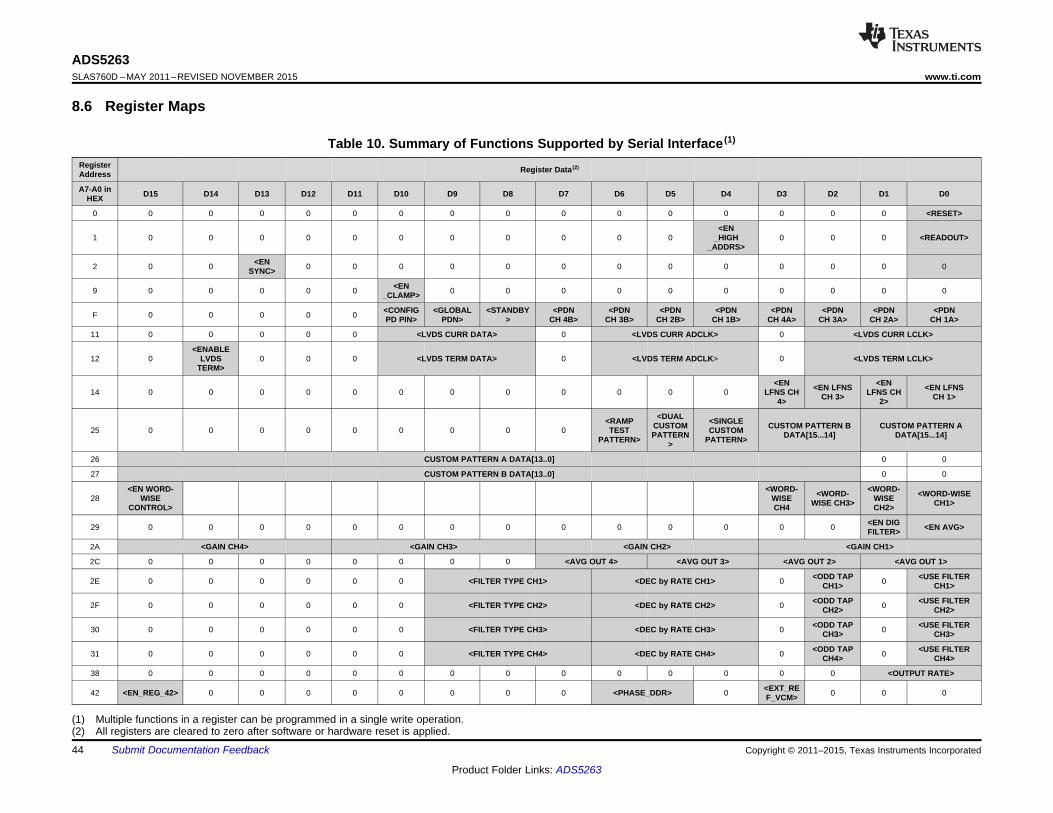
ADS5263SLAS760D –MAY 2011–REVISED NOVEMBER 2015 www.ti.com
8.6 Register Maps
Table 10. Summary of Functions Supported by Serial Interface (1)
Register Register Data(2)Address
A7-A0 in D15 D14 D13 D12 D11 D10 D9 D8 D7 D6 D5 D4 D3 D2 D1 D0HEX
0 0 0 0 0 0 0 0 0 0 0 0 0 0 0 0 <RESET>
<EN1 0 0 0 0 0 0 0 0 0 0 0 _HIGH 0 0 0 <READOUT>
_ADDRS>
<EN2 0 0 0 0 0 0 0 0 0 0 0 0 0 0 0SYNC>
<EN9 0 0 0 0 0 0 0 0 0 0 0 0 0 0 0_CLAMP>
<CONFIG <GLOBAL <STANDBY <PDN <PDN <PDN <PDN <PDN <PDN <PDN <PDNF 0 0 0 0 0 PD PIN> PDN> > CH 4B> CH 3B> CH 2B> CH 1B> CH 4A> CH 3A> CH 2A> CH 1A>
11 0 0 0 0 0 <LVDS CURR DATA> 0 <LVDS CURR ADCLK> 0 <LVDS CURR LCLK>
<ENABLE12 0 LVDS 0 0 0 <LVDS TERM DATA> 0 <LVDS TERM ADCLK> 0 <LVDS TERM LCLK>
TERM>
<EN <EN<EN LFNS <EN LFNS14 0 0 0 0 0 0 0 0 0 0 0 0 LFNS CH LFNS CHCH 3> CH 1>4> 2>
<DUAL<RAMP <SINGLECUSTOM CUSTOM PATTERN B CUSTOM PATTERN A25 0 0 0 0 0 0 0 0 0 TEST CUSTOMPATTERN DATA[15...14] DATA[15...14]PATTERN> PATTERN>>
26 CUSTOM PATTERN A DATA[13..0] 0 0
27 CUSTOM PATTERN B DATA[13..0] 0 0
<EN WORD- <WORD- <WORD-<WORD- <WORD-WISE28 WISE WISE WISEWISE CH3> CH1>CONTROL> CH4 CH2>
<EN DIG29 0 0 0 0 0 0 0 0 0 0 0 0 0 0 <EN AVG>FILTER>
2A <GAIN CH4> <GAIN CH3> <GAIN CH2> <GAIN CH1>
2C 0 0 0 0 0 0 0 0 <AVG OUT 4> <AVG OUT 3> <AVG OUT 2> <AVG OUT 1>
<ODD TAP <USE FILTER2E 0 0 0 0 0 0 <FILTER TYPE CH1> <DEC by RATE CH1> 0 0CH1> CH1>
<ODD TAP <USE FILTER2F 0 0 0 0 0 0 <FILTER TYPE CH2> <DEC by RATE CH2> 0 0CH2> CH2>
<ODD TAP <USE FILTER30 0 0 0 0 0 0 <FILTER TYPE CH3> <DEC by RATE CH3> 0 0CH3> CH3>
<ODD TAP <USE FILTER31 0 0 0 0 0 0 <FILTER TYPE CH4> <DEC by RATE CH4> 0 0CH4> CH4>
38 0 0 0 0 0 0 0 0 0 0 0 0 0 0 <OUTPUT RATE>
<EXT_RE42 <EN_REG_42> 0 0 0 0 0 0 0 0 <PHASE_DDR> 0 0 0 0F_VCM>
(1) Multiple functions in a register can be programmed in a single write operation.(2) All registers are cleared to zero after software or hardware reset is applied.
44 Submit Documentation Feedback Copyright © 2011–2015, Texas Instruments Incorporated
Product Folder Links: ADS5263
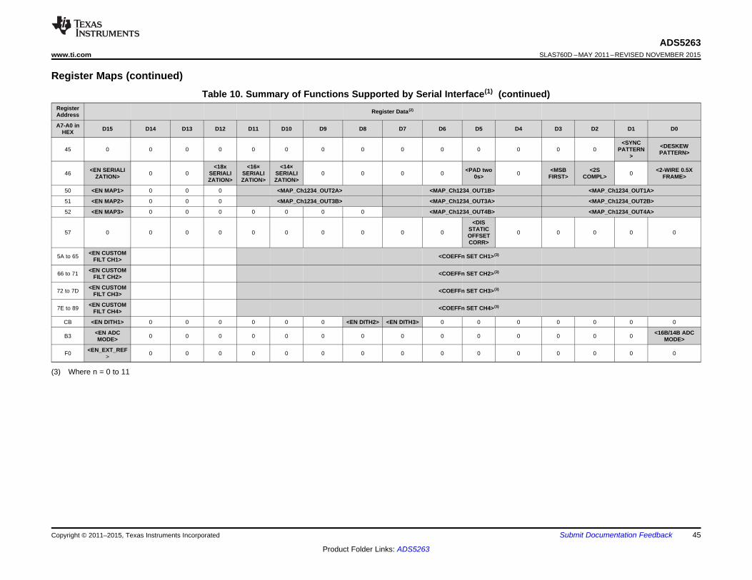
ADS5263www.ti.com SLAS760D –MAY 2011–REVISED NOVEMBER 2015
Register Maps (continued)Table 10. Summary of Functions Supported by Serial Interface(1) (continued)
Register Register Data(2)Address
A7-A0 in D15 D14 D13 D12 D11 D10 D9 D8 D7 D6 D5 D4 D3 D2 D1 D0HEX
<SYNC <DESKEW45 0 0 0 0 0 0 0 0 0 0 0 0 0 0 PATTERN PATTERN>>
<18x <16× <14×<EN SERIALI <PAD two <MSB <2S <2-WIRE 0.5X46 0 0 SERIALI SERIALI SERIALI 0 0 0 0 0 0ZATION> 0s> FIRST> COMPL> FRAME>ZATION> ZATION> ZATION>
50 <EN MAP1> 0 0 0 <MAP_Ch1234_OUT2A> <MAP_Ch1234_OUT1B> <MAP_Ch1234_OUT1A>
51 <EN MAP2> 0 0 0 <MAP_Ch1234_OUT3B> <MAP_Ch1234_OUT3A> <MAP_Ch1234_OUT2B>
52 <EN MAP3> 0 0 0 0 0 0 0 <MAP_Ch1234_OUT4B> <MAP_Ch1234_OUT4A>
<DISSTATIC57 0 0 0 0 0 0 0 0 0 0 0 0 0 0 0OFFSETCORR>
<EN CUSTOM5A to 65 <COEFFn SET CH1> (3)FILT CH1>
<EN CUSTOM66 to 71 <COEFFn SET CH2> (3)FILT CH2>
<EN CUSTOM72 to 7D <COEFFn SET CH3> (3)FILT CH3>
<EN CUSTOM7E to 89 <COEFFn SET CH4> (3)FILT CH4>
CB <EN DITH1> 0 0 0 0 0 0 <EN DITH2> <EN DITH3> 0 0 0 0 0 0 0
<EN ADC <16B/14B ADCB3 0 0 0 0 0 0 0 0 0 0 0 0 0 0MODE> MODE>
<EN_EXT_REFF0 0 0 0 0 0 0 0 0 0 0 0 0 0 0 0>
(3) Where n = 0 to 11
Copyright © 2011–2015, Texas Instruments Incorporated Submit Documentation Feedback 45
Product Folder Links: ADS5263

ADS5263SLAS760D –MAY 2011–REVISED NOVEMBER 2015 www.ti.com
8.6.1 Default State After Reset• Device is in normal operation mode with 16-bit ADC enabled for all 4 channels.• Output interface is 1-wire, 16× serialization with 8× bit clock and 1× frame clock frequency• Serial readout is disabled• PD pin is configured as global power-down pin• LVDS output current is set to 3.5 mA; internal termination is disabled.• Digital gain is set to 0 dB.• Digital modes such as LFNS, digital filters are disabled.
8.6.2 Description of Serial Registers
Figure 63. Register Address 0
REGISTER REGISTER DATAADDRESSA7–A0 D15 D14 D13 D12 D11 D10 D9 D8 D7 D6 D5 D4 D3 D2 D1 D0IN HEX
0 0 0 0 0 0 0 0 0 0 0 0 0 0 0 0 <RESET>
D0 <RESET>1 Software reset applied – resets all internal registers to their default values and self-clears to 0
Figure 64. Register Address 1
A7–A0 D1 D14 D13 D12 D11 D10 D9 D8 D7 D6 D5 D4 D3 D2 D1 D05IN HEX
1 0 0 0 0 0 0 0 0 0 0 0 <EN 0 0 0 <READOUT>_HIGH
_ADDRS>
D4 <EN_HIGH_ADDRS>See section External Reference Mode
D0 <READOUT>0 Serial readout of registers is disabled. Pin SDOUT is in the high-impedance state.1 Serial readout enabled, SDOUT pin functions as serial data readout.
Figure 65. Register Address 2
A7–A0 D15 D14 D13 D12 D11 D10 D9 D8 D7 D6 D5 D4 D3 D2 D1 D0IN HEX
2 0 0 <EN SYNC> 0 0 0 0 0 0 0 0 0 0 0 0 0
D13 <EN SYNC>0 SYNC pin is disabled.1 SYNC pin can be used to synchronize the decimation filters across channels and across multiple chips.
46 Submit Documentation Feedback Copyright © 2011–2015, Texas Instruments Incorporated
Product Folder Links: ADS5263

ADS5263www.ti.com SLAS760D –MAY 2011–REVISED NOVEMBER 2015
Figure 66. Register Address 9
A7–A0 D15 D14 D13 D12 D11 D10 D9 D8 D7 D6 D5 D4 D3 D2 D1 D0IN HEX
9 0 0 0 0 0 <EN 0 0 0 0 0 0 0 0 0 0_CLAMP>
D10 <EN_CLAMP>0 Internal clamp is disabled.1 Internal clamp is enabled. The clamp works only for the 14-bit ADC input pins. The clamping is
synchronized with the pulse applied on the SYNC pin (see Clamp Function for CCD Signals in theapplication section).
Figure 67. Register Address F
A7–A0 D15 D14 D13 D12 D11 D10 D9 D8 D7 D6 D5 D4 D3 D2 D1 D0IN HEX
F 0 0 0 0 0 <CON <GLO <STA <PDN <PDN <PDN <PDN <PDN <PDN <PDN <PDNFIG BAL ND CH CH CH CH CH CH CH CHPD PDN> BY> 4B> 3B> 2B> 1B> 4A> 3A> 2A> 1A>
PIN>
D10 <CONFIG PDN PIN> Can be used to configure PDN pin as global power down or standby0 PDN pin functions as global power down.1 PDN pin functions as standby.
D9 <GLOBAL PDN>0 Normal ADC operation1 Device is put in global power down. All four channels are powered down, including LVDS output data
and clock buffers.
D8 <STANDBY>0 Normal ADC operation1 Device is put in standby. All four ADCs are powered down. Internal PLL, LVDS bit clock, and frame
clock are running.
D7–D0 <PDN CH X> Individual channel power down0 Channel X is powered up.1 Channel X is powered down.
Copyright © 2011–2015, Texas Instruments Incorporated Submit Documentation Feedback 47
Product Folder Links: ADS5263

ADS5263SLAS760D –MAY 2011–REVISED NOVEMBER 2015 www.ti.com
Figure 68. Register Address 11
REGISTER REGISTER DATAADDRESSA7–A0 D15 D14 D13 D12 D11 D10 D9 D8 D7 D6 D5 D4 D3 D2 D1 D0IN HEX
11 0 0 0 0 0 <LVDS CURR DATA> 0 <LVDS CURR ADCLK> 0 <LVDS CURR LCLK>
D10–D8 <LVDS CURR DATA> LVDS current control for data buffers000 3.5 mA001 2.5 mA010 1.5 mA011 0.5 mA100 7.5 mA101 6.5 mA110 5.5 mA111 4.5 mAD6–D4 <LVDS CURR LCLK> LVDS current control for frame-clock buffer000 3.5 mA001 2.5 mA010 1.5 mA011 0.5 mA100 7.5 mA101 6.5 mA110 5.5 mA111 4.5 mAD2–D0 <LVDS CURR LCLK> LVDS current control for bit-clock buffer000 3.5 mA001 2.5 mA010 1.5 mA011 0.5 mA100 7.5 mA101 6.5 mA110 5.5 mA111 4.5 mA
48 Submit Documentation Feedback Copyright © 2011–2015, Texas Instruments Incorporated
Product Folder Links: ADS5263

ADS5263www.ti.com SLAS760D –MAY 2011–REVISED NOVEMBER 2015
Figure 69. Register Address 12
REGISTER REGISTER DATAADDRESSA7–A0 D15 D14 D13 D12 D11 D10 D9 D8 D7 D6 D5 D4 D3 D2 D1 D0IN HEX
12 0 <ENABLE 0 0 0 <LVDS TERM 0 <LVDS TERM 0 <LVDS TERM LCLK>LVDS DATA> ADCLK>
TERM>
D14 <ENABLE LVDS TERM>0 Internal termination disabled1 Internal termination enabledD10–D8 <LVDS TERM DATA> Internal LVDS termination for data buffers000 No internal termination001 150 Ω010 100 Ω011 60 Ω100 80 Ω101 55 Ω110 45 Ω111 35 ΩD6–D4 <LVDS TERM ADCLK> Internal LVDS termination for frame clock buffer000 No internal termination001 150 Ω010 100 Ω011 60 Ω100 80 Ω101 55 Ω110 45 Ω111 35 ΩD2–D0 <LVDS TERM LCLK> Internal LVDS termination for bit clock buffer000 No internal termination001 150 Ω010 100 Ω011 60 Ω100 80 Ω101 55 Ω110 45 Ω111 35 Ω
Copyright © 2011–2015, Texas Instruments Incorporated Submit Documentation Feedback 49
Product Folder Links: ADS5263
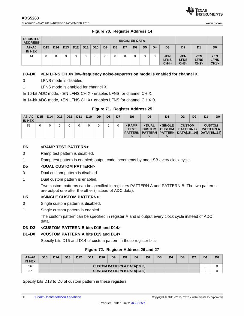
ADS5263SLAS760D –MAY 2011–REVISED NOVEMBER 2015 www.ti.com
Figure 70. Register Address 14
REGISTER REGISTER DATAADDRESSA7–A0 D15 D14 D13 D12 D11 D10 D9 D8 D7 D6 D5 D4 D3 D2 D1 D0IN HEX
14 0 0 0 0 0 0 0 0 0 0 0 0 <EN <EN <EN <ENLFNS LFNS LFNS LFNSCH4> CH3> CH2> CH1>
D3–D0 <EN LFNS CH X> low-frequency noise-suppression mode is enabled for channel X.0 LFNS mode is disabled.1 LFNS mode is enabled for channel X.In 16-bit ADC mode, <EN LFNS CH X> enables LFNS for channel CH X.In 14-bit ADC mode, <EN LFNS CH X> enables LFNS for channel CH X B.
Figure 71. Register Address 25
A7–A0 D15 D14 D13 D12 D11 D10 D9 D8 D7 D6 D5 D4 D3 D2 D1 D0IN HEX
25 0 0 0 0 0 0 0 0 0 <RAMP <DUAL <SINGLE CUSTOM CUSTOMTEST CUSTOM CUSTOM PATTERN B PATTERN A
PATTERN PATTERN PATTERN DATA[15...14] DATA[15...14]> > >
D6 <RAMP TEST PATTERN>0 Ramp test pattern is disabled.1 Ramp test pattern is enabled; output code increments by one LSB every clock cycle.D5 <DUAL CUSTOM PATTERN>0 Dual custom pattern is disabled.1 Dual custom pattern is enabled.
Two custom patterns can be specified in registers PATTERN A and PATTERN B. The two patternsare output one after the other (instead of ADC data).
D5 <SINGLE CUSTOM PATTERN>0 Single custom pattern is disabled.1 Single custom pattern is enabled.
The custom pattern can be specified in register A and is output every clock cycle instead of ADCdata.
D3–D2 <CUSTOM PATTERN B bits D15 and D14>D1–D0 <CUSTOM PATTERN A bits D15 and D14>
Specify bits D15 and D14 of custom pattern in these register bits.
Figure 72. Register Address 26 and 27
A7–A0 D15 D14 D13 D12 D11 D10 D9 D8 D7 D6 D5 D4 D3 D2 D1 D0IN HEX
26 CUSTOM PATTERN A DATA[13..0] 0 027 CUSTOM PATTERN B DATA[13..0] 0 0
Specify bits D13 to D0 of custom pattern in these registers.
50 Submit Documentation Feedback Copyright © 2011–2015, Texas Instruments Incorporated
Product Folder Links: ADS5263
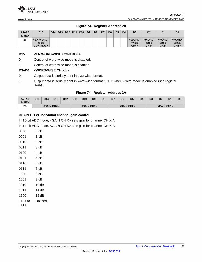
ADS5263www.ti.com SLAS760D –MAY 2011–REVISED NOVEMBER 2015
Figure 73. Register Address 28
A7–A0 D15 D14 D13 D12 D11 D10 D9 D8 D7 D6 D5 D4 D3 D2 D1 D0IN HEX
28 <EN WORD- <WORD- <WORD- <WORD- <WORD-WISE WISE WISE WISE WISE
CONTROL> CH4> CH3> CH2> CH1>
D15 <EN WORD-WISE CONTROL>0 Control of word-wise mode is disabled.1 Control of word-wise mode is enabled.D3–D0 <WORD-WISE CH XL>0 Output data is serially sent in byte-wise format.1 Output data is serially sent in word-wise format ONLY when 2-wire mode is enabled (see register
0x46).
Figure 74. Register Address 2A
A7–A0 D15 D14 D13 D12 D11 D10 D9 D8 D7 D6 D5 D4 D3 D2 D1 D0IN HEX
2A <GAIN CH4> <GAIN CH3> <GAIN CH2> <GAIN CH1>
<GAIN CH x> Individual channel gain controlIn 16-bit ADC mode, <GAIN CH X> sets gain for channel CH X A.In 14-bit ADC mode, <GAIN CH X> sets gain for channel CH X B.0000 0 dB0001 1 dB0010 2 dB0011 3 dB0100 4 dB0101 5 dB0110 6 dB0111 7 dB1000 8 dB1001 9 dB1010 10 dB1011 11 dB1100 12 dB1101 to Unused1111
Copyright © 2011–2015, Texas Instruments Incorporated Submit Documentation Feedback 51
Product Folder Links: ADS5263

ADS5263SLAS760D –MAY 2011–REVISED NOVEMBER 2015 www.ti.com
Figure 75. Register Address 2C
A7–A0 D15 D14 D13 D12 D11 D10 D9 D8 D7 D6 D5 D4 D3 D2 D1 D0IN HEX
2C 0 0 0 0 0 0 0 0 <AVG OUT 4> <AVG OUT 3> <AVG OUT 2> <AVG OUT 1>
<AVG OUT 1> These bits determine which data stream is output on LVDS pins OUT1A/1B.(after global enable bit for averaging is enabled <EN AVG GLO> = 1)
00 LVDS OUT1A/1B buffers are powered down.01 OUT1A/1B output digital data corresponding to the signal applied on analog input pin IN1.10 OUT1A/1B output digital data corresponding to the average of signals applied on analog
input pins IN1 and IN2.11 OUT1A/1B output digital data corresponding to the average of signals applied on analog
input pins IN1, IN2, IN3, and IN4.<AVG OUT 2> These bits determine which data stream is output on LVDS pins OUT2A/2B
(after global enable bit for averaging is enabled <EN AVG GLO> = 1)00 LVDS OUT2A/2B buffers are powered down.01 OUT2A/2B output digital data corresponding to the signal applied on analog input pin IN2.10 OUT2A/2B output digital data corresponding to the signal applied on analog input pin IN3.11 OUT2A/2B output digital data corresponding to the average of signals applied on analog
input pins IN3 and IN4.<AVG OUT 3> These bits determine which data stream is output on LVDS pins OUT3A/3B
(after global enable bit for averaging is enabled <EN AVG GLO> = 1)00 LVDS OUT3A/3B buffers are powered down.01 OUT3A/3B output digital data corresponding to the signal applied on analog input pin IN3.10 OUT3A/3B output digital data corresponding to the signal applied on analog input pin IN2.11 OUT3A/3B output digital data corresponding to the average of signals applied on analog
input pins IN1 and IN4.<AVG OUT 4> These bits determine which data stream is output on LVDS pins OUT4A/4B
(after global enable bit for averaging is enabled <EN AVG GLO> = 1)00 LVDS OUT4A/4B buffers are powered down.01 OUT4A/4B output digital data corresponding to the signal applied on analog input pin IN4.10 OUT4A/4B output digital data corresponding to the average of signals applied on analog
input pins IN3 and IN4.11 OUT4A/4B output digital data corresponding to the average of signals applied on analog
input pins IN1, IN2, IN3, and IN4.
52 Submit Documentation Feedback Copyright © 2011–2015, Texas Instruments Incorporated
Product Folder Links: ADS5263
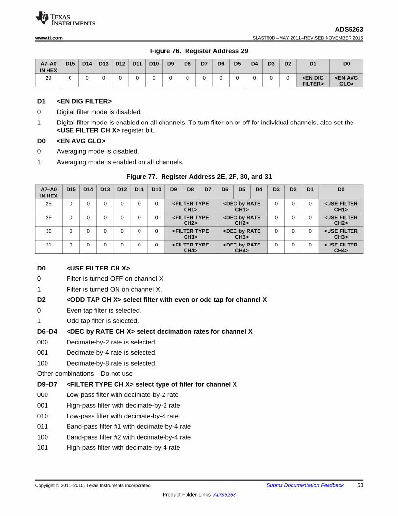
ADS5263www.ti.com SLAS760D –MAY 2011–REVISED NOVEMBER 2015
Figure 76. Register Address 29
A7–A0 D15 D14 D13 D12 D11 D10 D9 D8 D7 D6 D5 D4 D3 D2 D1 D0IN HEX
29 0 0 0 0 0 0 0 0 0 0 0 0 0 0 <EN DIG <EN AVGFILTER> GLO>
D1 <EN DIG FILTER>0 Digital filter mode is disabled.1 Digital filter mode is enabled on all channels. To turn filter on or off for individual channels, also set the
<USE FILTER CH X> register bit.D0 <EN AVG GLO>0 Averaging mode is disabled.1 Averaging mode is enabled on all channels.
Figure 77. Register Address 2E, 2F, 30, and 31
A7–A0 D15 D14 D13 D12 D11 D10 D9 D8 D7 D6 D5 D4 D3 D2 D1 D0IN HEX
2E 0 0 0 0 0 0 <FILTER TYPE <DEC by RATE 0 0 0 <USE FILTERCH1> CH1> CH1>
2F 0 0 0 0 0 0 <FILTER TYPE <DEC by RATE 0 0 0 <USE FILTERCH2> CH2> CH2>
30 0 0 0 0 0 0 <FILTER TYPE <DEC by RATE 0 0 0 <USE FILTERCH3> CH3> CH3>
31 0 0 0 0 0 0 <FILTER TYPE <DEC by RATE 0 0 0 <USE FILTERCH4> CH4> CH4>
D0 <USE FILTER CH X>0 Filter is turned OFF on channel X1 Filter is turned ON on channel X.D2 <ODD TAP CH X> select filter with even or odd tap for channel X0 Even tap filter is selected.1 Odd tap filter is selected.D6–D4 <DEC by RATE CH X> select decimation rates for channel X000 Decimate-by-2 rate is selected.001 Decimate-by-4 rate is selected.100 Decimate-by-8 rate is selected.Other combinations x Do not useD9–D7 <FILTER TYPE CH X> select type of filter for channel X000 Low-pass filter with decimate-by-2 rate001 High-pass filter with decimate-by-2 rate010 Low-pass filter with decimate-by-4 rate011 Band-pass filter #1 with decimate-by-4 rate100 Band-pass filter #2 with decimate-by-4 rate101 High-pass filter with decimate-by-4 rate
Copyright © 2011–2015, Texas Instruments Incorporated Submit Documentation Feedback 53
Product Folder Links: ADS5263

ADS5263SLAS760D –MAY 2011–REVISED NOVEMBER 2015 www.ti.com
Figure 78. Register Address 38
A7–A0 D15 D14 D13 D12 D11 D10 D9 D8 D7 D6 D5 D4 D3 D2 D1 D0IN HEX
38 0 0 0 0 0 0 0 0 0 0 0 0 0 0 <OUTPUT RATE>
D1–D0 <OUTPUT RATE>00 Output data rate = 1× sample rate01 Output data rate = 0.5× sample rate02 Output data rate = 0.25× sample rate03 Output data rate = 0.125× sample rate
Figure 79. Register Address 42
REGISTER REGISTER DATAADDRESS
A7–A0 D15 D14 D13 D12 D11 D1 D9 D8 D7 D6 D5 D4 D3 D2 D1 D00IN HEX
42 <EN_REG_4 0 0 0 0 0 0 0 0 <PHASE_ 0 <EXT_REF_ 0 0 02> DDR> VCM>
D15 <EN_REG_42>0 Disables register bits D6, D5 and D31 Enables register bits D6, D5 and D3D6-D5 <PHASE_DDR>
Note that the default value of <PHASE_DDR> bit = 10. However, in this condition, if the contents ofthe register 0x42 are readout, they will be read as 00.If the value of <PHASE_DDR> bit is now modified by writing into this resgister, then subsequentwrites will read back the written value.Register bit <PHASE_DDR> can be used to control the phase of LCLK (with respect to the risingedge of the frame clock, ADCLK). See Programmable LCLK Phase for details.
D3 EXT_REF_VCM0 Internal reference mode1 External reference mode, Apply voltage on VCM input
See section External Reference ModeTo use this mode, the register bit <EN_EXT_REF> in register 0xF0 must also be set to 1.
54 Submit Documentation Feedback Copyright © 2011–2015, Texas Instruments Incorporated
Product Folder Links: ADS5263

ADS5263www.ti.com SLAS760D –MAY 2011–REVISED NOVEMBER 2015
Figure 80. Register Address 45
A7–A0 D15 D14 D13 D12 D11 D10 D9 D8 D7 D6 D5 D4 D3 D2 D1 D0IN HEX
45 0 0 0 0 0 0 0 0 0 0 0 0 0 0 <SYNC <DESKEWPATTERN> PATTERN>
D1 <SYNC PATTERN>0 Sync pattern disabled.1 Sync pattern enabled.
All channels output a repeating pattern of 8 1s and 8 0s instead of ADC data.Output data [15…0] = 0xFF00
D0 <DESKEW PATTERN>0 Deskew pattern disabled.1 Deskew pattern enabled.
All channels output a repeating pattern of 1010101010101010 instead of ADC data.
Copyright © 2011–2015, Texas Instruments Incorporated Submit Documentation Feedback 55
Product Folder Links: ADS5263

ADS5263SLAS760D –MAY 2011–REVISED NOVEMBER 2015 www.ti.com
Figure 81. Register Address 46
A7-A0 D15 D D1 D12 D11 D10 D9 D8 D7 D6 D5 D D3 D2 D D014 3 4 1IN
HEX46 <ENABLE 0 0 <18b <16b <14b 0 0 0 0 <PAD 0 <MSB <2S 0 <2-WIRE
SERIALI SERIALI SERIALI SERIALI two FIRST COMPL 0.5XZATION> ZATION> ZATION> ZATION> 0s> > > FRAME>
D15 <ENABLE SERIALIZATION> Enable bit for serialization bits in register 46>0 Disable control of serialization register bits in register 0x46.1 Enable control of serialization register bits in register 0x46.D12 <18b SERIALIZATION> Enable 18-bit serialization, to be used to send 18-bit data when using
digital processing modes (see section Performance with Digital Processing Blocks)0 Disable 18-bit serialization.1 Enable 18-bit serialization. ADC data bits D[17..0] are serialized.D11 <16b SERIALIZATION> Enable 16-bit serialization, to be used in 16-bit ADC mode0 Disable 16-bit serialization.1 Enable 16-bit serialization. ADC data bits D[15..0] are serialized.D10 <14b SERIALIZATION> Enable 14-bit serialization, to be used in 14-bit ADC mode0 Disable 14-bit serialization.1 Enable 14-bit serialization. ADC data bits D[13..0] are serialized.D5 <PAD two 0s>0 Padding disabled.1 Two zero bits are padded to the ADC data on the LSB side and the combined data is then serialized.
When the bit <4b SERIALIZATION> is also enabled, two zero bits are padded to the 14-bit ADC data.The combined data (= ADC[13..0],0,0) is serially output.
D3 <MSB First>0 ADC data is output serially, with LSB bit first.1 ADC data is output serially, with MSB bit first.D2 <2s COMPL>0 Output data format is offset binary.1 Output data format is 2s complement.D0 <2-WIRE 0.5× frame clock>0 Enables 1-wire LVDS interface with 1× frame clock.1 Enables 2-wire LVDS interface with 0.5× frame clock.
56 Submit Documentation Feedback Copyright © 2011–2015, Texas Instruments Incorporated
Product Folder Links: ADS5263
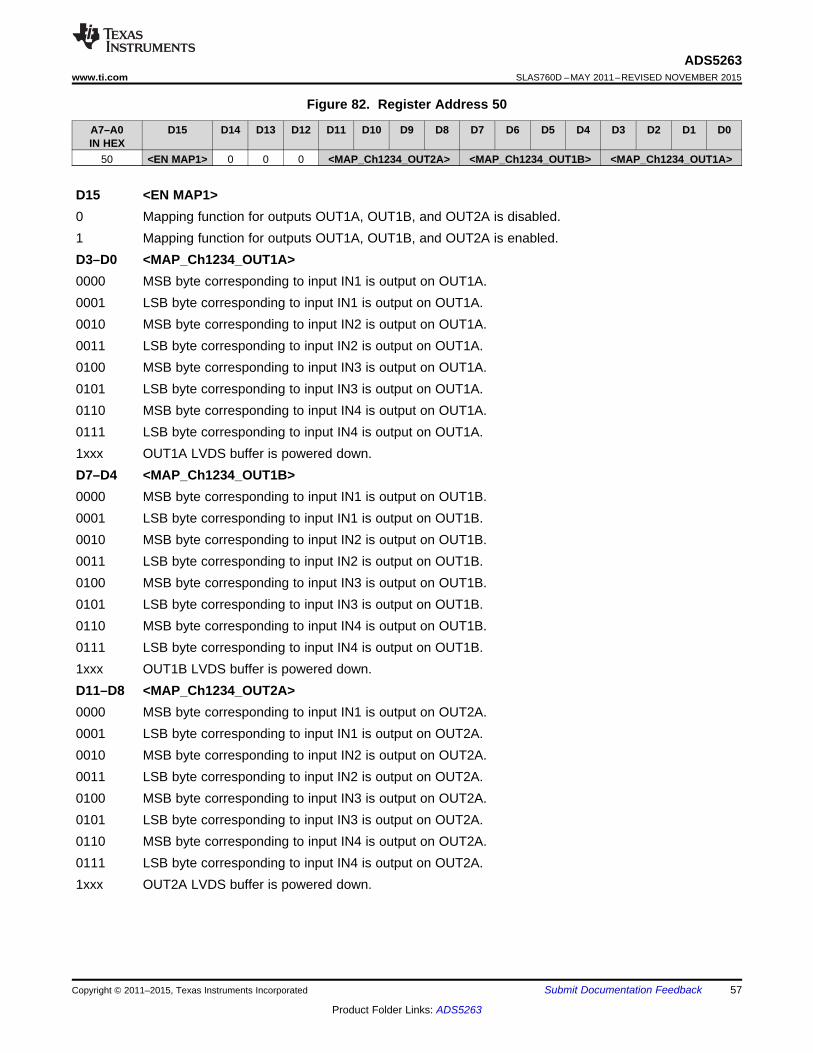
ADS5263www.ti.com SLAS760D –MAY 2011–REVISED NOVEMBER 2015
Figure 82. Register Address 50
A7–A0 D15 D14 D13 D12 D11 D10 D9 D8 D7 D6 D5 D4 D3 D2 D1 D0IN HEX
50 <EN MAP1> 0 0 0 <MAP_Ch1234_OUT2A> <MAP_Ch1234_OUT1B> <MAP_Ch1234_OUT1A>
D15 <EN MAP1>0 Mapping function for outputs OUT1A, OUT1B, and OUT2A is disabled.1 Mapping function for outputs OUT1A, OUT1B, and OUT2A is enabled.D3–D0 <MAP_Ch1234_OUT1A>0000 MSB byte corresponding to input IN1 is output on OUT1A.0001 LSB byte corresponding to input IN1 is output on OUT1A.0010 MSB byte corresponding to input IN2 is output on OUT1A.0011 LSB byte corresponding to input IN2 is output on OUT1A.0100 MSB byte corresponding to input IN3 is output on OUT1A.0101 LSB byte corresponding to input IN3 is output on OUT1A.0110 MSB byte corresponding to input IN4 is output on OUT1A.0111 LSB byte corresponding to input IN4 is output on OUT1A.1xxx OUT1A LVDS buffer is powered down.D7–D4 <MAP_Ch1234_OUT1B>0000 MSB byte corresponding to input IN1 is output on OUT1B.0001 LSB byte corresponding to input IN1 is output on OUT1B.0010 MSB byte corresponding to input IN2 is output on OUT1B.0011 LSB byte corresponding to input IN2 is output on OUT1B.0100 MSB byte corresponding to input IN3 is output on OUT1B.0101 LSB byte corresponding to input IN3 is output on OUT1B.0110 MSB byte corresponding to input IN4 is output on OUT1B.0111 LSB byte corresponding to input IN4 is output on OUT1B.1xxx OUT1B LVDS buffer is powered down.D11–D8 <MAP_Ch1234_OUT2A>0000 MSB byte corresponding to input IN1 is output on OUT2A.0001 LSB byte corresponding to input IN1 is output on OUT2A.0010 MSB byte corresponding to input IN2 is output on OUT2A.0011 LSB byte corresponding to input IN2 is output on OUT2A.0100 MSB byte corresponding to input IN3 is output on OUT2A.0101 LSB byte corresponding to input IN3 is output on OUT2A.0110 MSB byte corresponding to input IN4 is output on OUT2A.0111 LSB byte corresponding to input IN4 is output on OUT2A.1xxx OUT2A LVDS buffer is powered down.
Copyright © 2011–2015, Texas Instruments Incorporated Submit Documentation Feedback 57
Product Folder Links: ADS5263
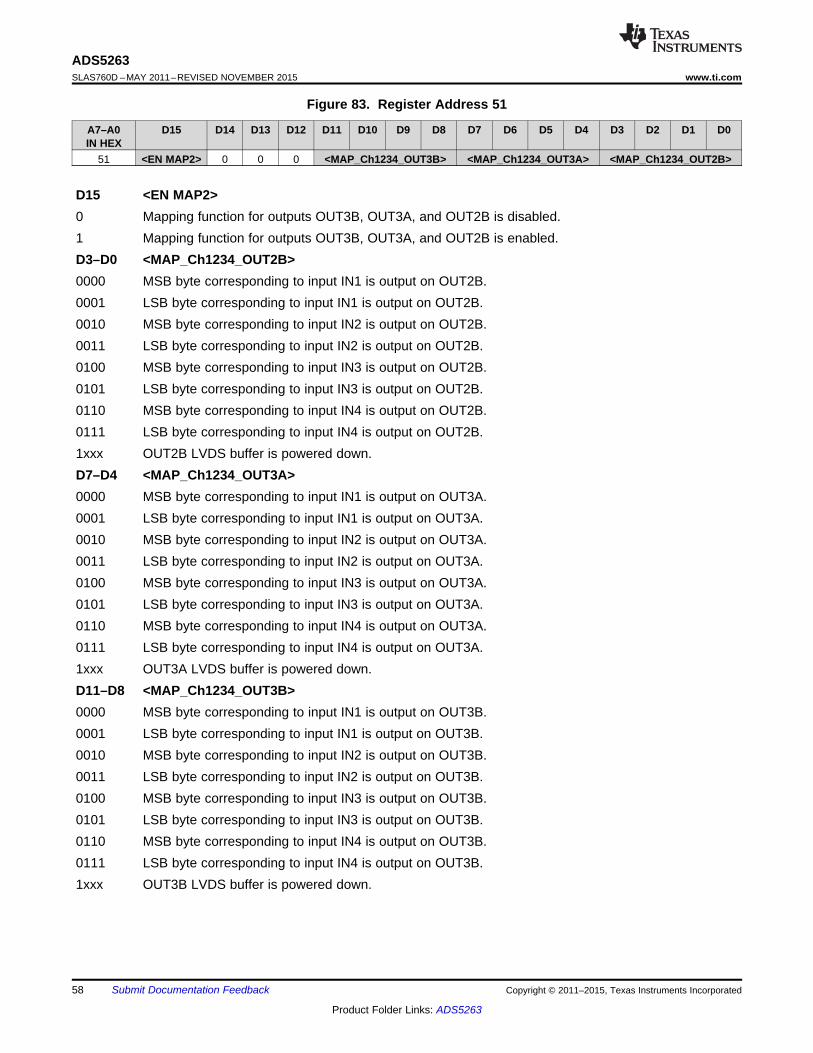
ADS5263SLAS760D –MAY 2011–REVISED NOVEMBER 2015 www.ti.com
Figure 83. Register Address 51
A7–A0 D15 D14 D13 D12 D11 D10 D9 D8 D7 D6 D5 D4 D3 D2 D1 D0IN HEX
51 <EN MAP2> 0 0 0 <MAP_Ch1234_OUT3B> <MAP_Ch1234_OUT3A> <MAP_Ch1234_OUT2B>
D15 <EN MAP2>0 Mapping function for outputs OUT3B, OUT3A, and OUT2B is disabled.1 Mapping function for outputs OUT3B, OUT3A, and OUT2B is enabled.D3–D0 <MAP_Ch1234_OUT2B>0000 MSB byte corresponding to input IN1 is output on OUT2B.0001 LSB byte corresponding to input IN1 is output on OUT2B.0010 MSB byte corresponding to input IN2 is output on OUT2B.0011 LSB byte corresponding to input IN2 is output on OUT2B.0100 MSB byte corresponding to input IN3 is output on OUT2B.0101 LSB byte corresponding to input IN3 is output on OUT2B.0110 MSB byte corresponding to input IN4 is output on OUT2B.0111 LSB byte corresponding to input IN4 is output on OUT2B.1xxx OUT2B LVDS buffer is powered down.D7–D4 <MAP_Ch1234_OUT3A>0000 MSB byte corresponding to input IN1 is output on OUT3A.0001 LSB byte corresponding to input IN1 is output on OUT3A.0010 MSB byte corresponding to input IN2 is output on OUT3A.0011 LSB byte corresponding to input IN2 is output on OUT3A.0100 MSB byte corresponding to input IN3 is output on OUT3A.0101 LSB byte corresponding to input IN3 is output on OUT3A.0110 MSB byte corresponding to input IN4 is output on OUT3A.0111 LSB byte corresponding to input IN4 is output on OUT3A.1xxx OUT3A LVDS buffer is powered down.D11–D8 <MAP_Ch1234_OUT3B>0000 MSB byte corresponding to input IN1 is output on OUT3B.0001 LSB byte corresponding to input IN1 is output on OUT3B.0010 MSB byte corresponding to input IN2 is output on OUT3B.0011 LSB byte corresponding to input IN2 is output on OUT3B.0100 MSB byte corresponding to input IN3 is output on OUT3B.0101 LSB byte corresponding to input IN3 is output on OUT3B.0110 MSB byte corresponding to input IN4 is output on OUT3B.0111 LSB byte corresponding to input IN4 is output on OUT3B.1xxx OUT3B LVDS buffer is powered down.
58 Submit Documentation Feedback Copyright © 2011–2015, Texas Instruments Incorporated
Product Folder Links: ADS5263

ADS5263www.ti.com SLAS760D –MAY 2011–REVISED NOVEMBER 2015
Figure 84. Register Address 52
A7–A0 D15 D14 D13 D12 D11 D10 D9 D8 D7 D6 D5 D4 D3 D2 D1 D0IN HEX
52 <EN MAP3> 0 0 0 0 0 0 0 <MAP_Ch1234_OUT4B> <MAP_Ch1234_OUT4B>
D15 <EN MAP3>0 Mapping function for outputs OUT4A and OUT4B is disabled.1 Mapping function for outputs OUT4A and OUT4B is enabled.D3–D0 <MAP_Ch1234_OUT4A>0000 MSB byte corresponding to input IN1 is output on OUT4A.0001 LSB byte corresponding to input IN1 is output on OUT4A.0010 MSB byte corresponding to input IN2 is output on OUT4A.0011 LSB byte corresponding to input IN2 is output on OUT4A.0100 MSB byte corresponding to input IN3 is output on OUT4A.0101 LSB byte corresponding to input IN3 is output on OUT4A.0110 MSB byte corresponding to input IN4 is output on OUT4A.0111 LSB byte corresponding to input IN4 is output on OUT4A.1xxx OUT4A LVDS buffer is powered down.D7–D4 <MAP_Ch1234_OUT4B>0000 MSB byte corresponding to input IN1 is output on OUT4B.0001 LSB byte corresponding to input IN1 is output on OUT4B.0010 MSB byte corresponding to input IN2 is output on OUT4B.0011 LSB byte corresponding to input IN2 is output on OUT4B.0100 MSB byte corresponding to input IN3 is output on OUT4B.0101 LSB byte corresponding to input IN3 is output on OUT4B.0110 MSB byte corresponding to input IN4 is output on OUT4B.0111 LSB byte corresponding to input IN4 is output on OUT4B.1xxx OUT4B LVDS buffer is powered down.
Figure 85. Register Address 57
A7–A0 D15 D14 D13 D12 D11 D10 D9 D8 D7 D6 D5 D4 D3 D2 D1 D0IN HEX
57 0 0 0 0 0 0 0 0 0 0 <DIS STATIC 0 0 0 0 0OFFSET CORR>
D5 <DIS STATIC OFFSET CORR> Disables algorithm to correct static offset in sub-ranging flash ADCinside pipeline, to be used in imaging applications where ADC is used to convert DC signal
0 Algorithm is active.1 Algorithm is disabled.
Copyright © 2011–2015, Texas Instruments Incorporated Submit Documentation Feedback 59
Product Folder Links: ADS5263

ADS5263SLAS760D –MAY 2011–REVISED NOVEMBER 2015 www.ti.com
Figure 86. Register Address 5A to 65, 66 to 71, 72 to 7D, and 7E to 89
A7–A0 D15 D14 D13 D12 D11 D10 D9 D8 D7 D6 D5 D4 D3 D2 D1 D0IN HEX5A to 65 <EN 0 0 0 <COEFFn SET CH1>
CUSTOMFILT CH1>
66 to 71 <EN <COEFFn SET CH2>CUSTOM
FILT CH2>72 to 7D <EN <COEFFn SET CH3>
CUSTOMFILT CH3>
7E to 89 <EN <COEFFn SET CH4>CUSTOM
FILT CH4>
D15 <EN CUSTOM FILT CH1> to <EN CUSTOM FILT CH4>For description of these registers see Table 4.
D11–D0 <COEFFn SET CH1> to <COEFFn SET CH4>For description of these registers see Table 4.
Figure 87. Register Address CB
A7–A0 D15 D14 D13 D12 D11 D10 D9 D8 D7 D6 D5 D4 D3 D2 D1 D0IN HEX
CB <EN 0 0 0 0 0 0 <EN <EN 0 0 0 0 0 0 0DITH1> DITH2> DITH3>
D15, D8, D7 <EN DITH1:3> Enable bits for dither algorithmSet register bit EN_HIGH_ADDRS to 1 before programming these bits.000 Dither algorithm is disabled.111 Dither algorithm is enabled for all channels.
Using dither algorithm improves INL curve.However, it may degrade the noise by as much as 3dB.
Figure 88. Register Address B3
A7–A0 D15 D14 D13 D12 D11 D10 D9 D8 D7 D6 D5 D4 D3 D2 D1 D0IN HEX
B3 <ENABLE 0 0 0 0 0 0 0 0 0 0 0 0 0 0 <16B/14BADC MODE> ADC MODE>
D15 <ENABLE ADC MODE>0 Disable selection of 14-bit ADC mode.1 Enables selection of 14 bit ADC mode.D0 <16B/14B ADC MODE>0 16-bit ADC operation is enabled.1 14-bit ADC operation is enabled.
60 Submit Documentation Feedback Copyright © 2011–2015, Texas Instruments Incorporated
Product Folder Links: ADS5263
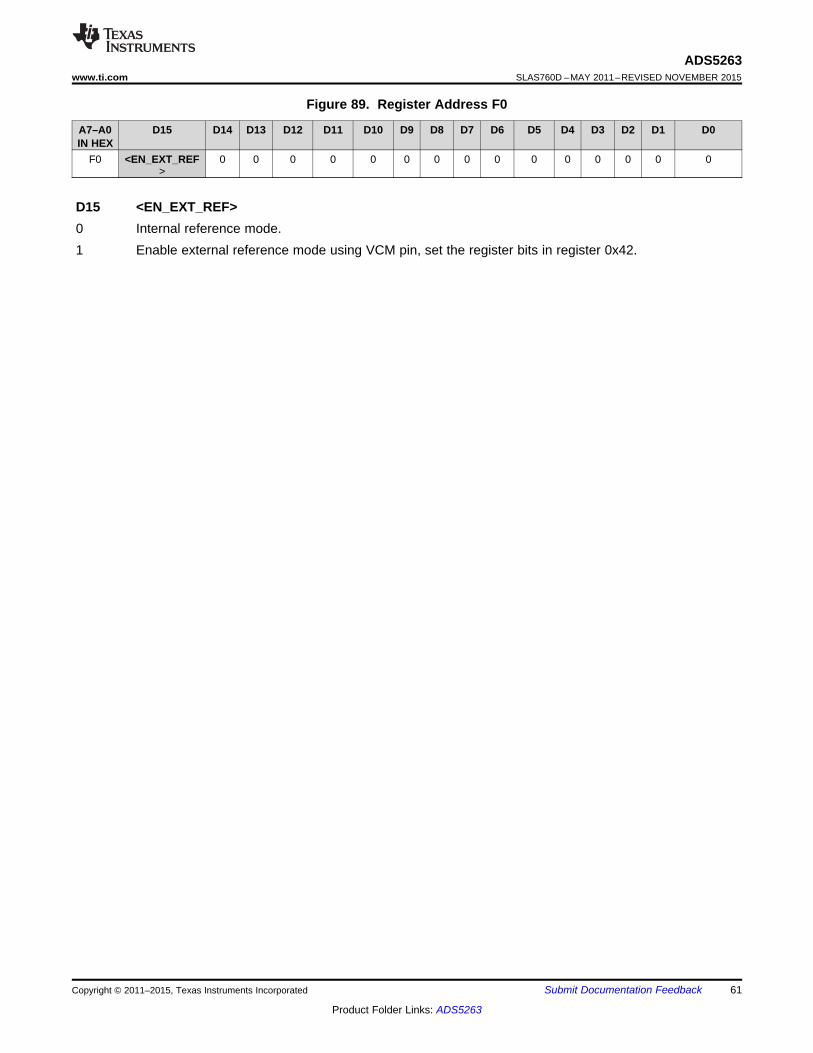
ADS5263www.ti.com SLAS760D –MAY 2011–REVISED NOVEMBER 2015
Figure 89. Register Address F0
A7–A0 D15 D14 D13 D12 D11 D10 D9 D8 D7 D6 D5 D4 D3 D2 D1 D0IN HEX
F0 <EN_EXT_REF 0 0 0 0 0 0 0 0 0 0 0 0 0 0 0>
D15 <EN_EXT_REF>0 Internal reference mode.1 Enable external reference mode using VCM pin, set the register bits in register 0x42.
Copyright © 2011–2015, Texas Instruments Incorporated Submit Documentation Feedback 61
Product Folder Links: ADS5263
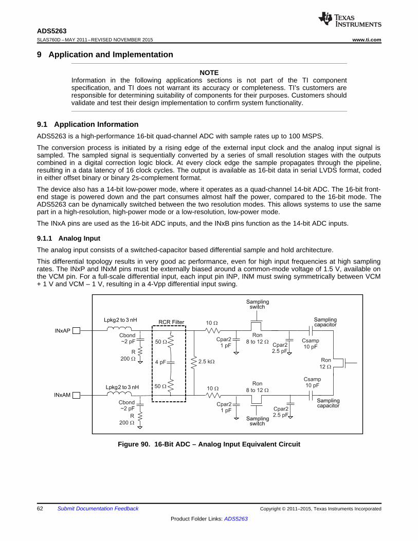
INxAP
INxAMSamplingcapacitor
Samplingswitch
Samplingswitch
Lpkg2 to 3 nH Samplingcapacitor
Lpkg2 to 3 nH
RCR Filter
Cbond~2 pF
R
200 W
R
200 W
50 W
50 W
4 pF
10 W
2.5 kW
10 W
Cpar21 pF
Cpar21 pF
Ron
8 to 12 W
Ron
8 to 12 W
Cpar22.5 pF
Cpar22.5 pF
Cbond~2 pF
Csamp10 pF
Csamp10 pF
Ron
12 W
ADS5263SLAS760D –MAY 2011–REVISED NOVEMBER 2015 www.ti.com
9 Application and Implementation
NOTEInformation in the following applications sections is not part of the TI componentspecification, and TI does not warrant its accuracy or completeness. TI’s customers areresponsible for determining suitability of components for their purposes. Customers shouldvalidate and test their design implementation to confirm system functionality.
9.1 Application InformationADS5263 is a high-performance 16-bit quad-channel ADC with sample rates up to 100 MSPS.
The conversion process is initiated by a rising edge of the external input clock and the analog input signal issampled. The sampled signal is sequentially converted by a series of small resolution stages with the outputscombined in a digital correction logic block. At every clock edge the sample propagates through the pipeline,resulting in a data latency of 16 clock cycles. The output is available as 16-bit data in serial LVDS format, codedin either offset binary or binary 2s-complement format.
The device also has a 14-bit low-power mode, where it operates as a quad-channel 14-bit ADC. The 16-bit front-end stage is powered down and the part consumes almost half the power, compared to the 16-bit mode. TheADS5263 can be dynamically switched between the two resolution modes. This allows systems to use the samepart in a high-resolution, high-power mode or a low-resolution, low-power mode.
The INxA pins are used as the 16-bit ADC inputs, and the INxB pins function as the 14-bit ADC inputs.
9.1.1 Analog InputThe analog input consists of a switched-capacitor based differential sample and hold architecture.
This differential topology results in very good ac performance, even for high input frequencies at high samplingrates. The INxP and INxM pins must be externally biased around a common-mode voltage of 1.5 V, available onthe VCM pin. For a full-scale differential input, each input pin INP, INM must swing symmetrically between VCM+ 1 V and VCM – 1 V, resulting in a 4-Vpp differential input swing.
Figure 90. 16-Bit ADC – Analog Input Equivalent Circuit
62 Submit Documentation Feedback Copyright © 2011–2015, Texas Instruments Incorporated
Product Folder Links: ADS5263
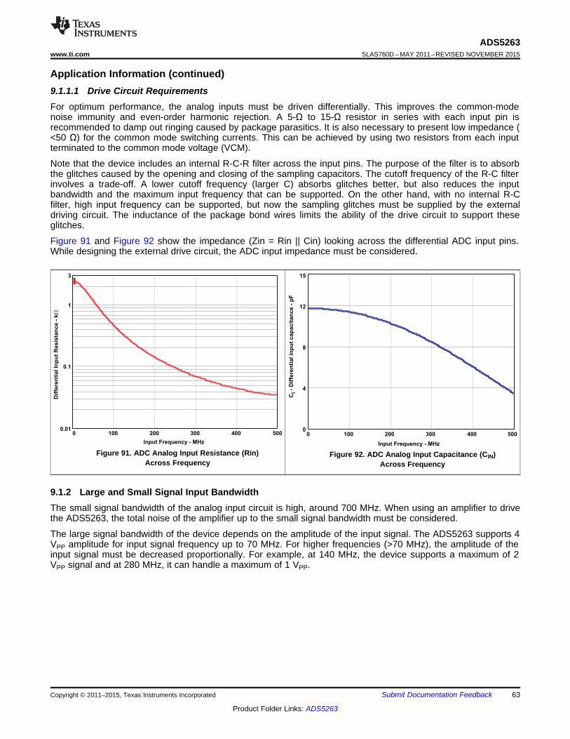
100 200 300 4000 500
4
8
12
0
15
Input Frequency - MHz
C-
Dif
fere
nti
al in
pu
t cap
acit
an
ce -
pF
I
100 200 300 4000 500
0.1
1
0.01
3
Input Frequency - MHz
Dif
fere
nti
al In
pu
t R
esis
tan
ce -
kW
ADS5263www.ti.com SLAS760D –MAY 2011–REVISED NOVEMBER 2015
Application Information (continued)9.1.1.1 Drive Circuit RequirementsFor optimum performance, the analog inputs must be driven differentially. This improves the common-modenoise immunity and even-order harmonic rejection. A 5-Ω to 15-Ω resistor in series with each input pin isrecommended to damp out ringing caused by package parasitics. It is also necessary to present low impedance (<50 Ω) for the common mode switching currents. This can be achieved by using two resistors from each inputterminated to the common mode voltage (VCM).
Note that the device includes an internal R-C-R filter across the input pins. The purpose of the filter is to absorbthe glitches caused by the opening and closing of the sampling capacitors. The cutoff frequency of the R-C filterinvolves a trade-off. A lower cutoff frequency (larger C) absorbs glitches better, but also reduces the inputbandwidth and the maximum input frequency that can be supported. On the other hand, with no internal R-Cfilter, high input frequency can be supported, but now the sampling glitches must be supplied by the externaldriving circuit. The inductance of the package bond wires limits the ability of the drive circuit to support theseglitches.
Figure 91 and Figure 92 show the impedance (Zin = Rin || Cin) looking across the differential ADC input pins.While designing the external drive circuit, the ADC input impedance must be considered.
Figure 91. ADC Analog Input Resistance (Rin) Figure 92. ADC Analog Input Capacitance (CIN)Across Frequency Across Frequency
9.1.2 Large and Small Signal Input BandwidthThe small signal bandwidth of the analog input circuit is high, around 700 MHz. When using an amplifier to drivethe ADS5263, the total noise of the amplifier up to the small signal bandwidth must be considered.
The large signal bandwidth of the device depends on the amplitude of the input signal. The ADS5263 supports 4VPP amplitude for input signal frequency up to 70 MHz. For higher frequencies (>70 MHz), the amplitude of theinput signal must be decreased proportionally. For example, at 140 MHz, the device supports a maximum of 2VPP signal and at 280 MHz, it can handle a maximum of 1 VPP.
Copyright © 2011–2015, Texas Instruments Incorporated Submit Documentation Feedback 63
Product Folder Links: ADS5263
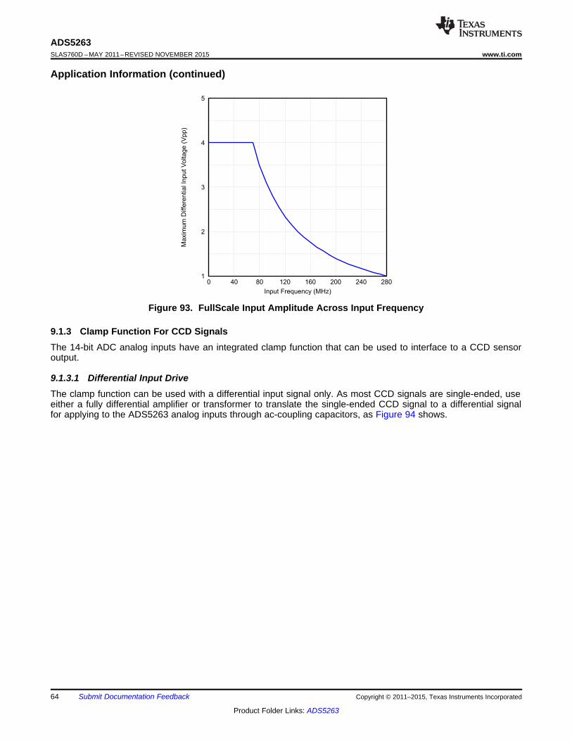
1
2
3
4
5
0 40 80 120 160 200 240 280
Input Frequency (MHz)
Maxim
um
Diffe
rential In
put V
oltage (
Vpp)
ADS5263SLAS760D –MAY 2011–REVISED NOVEMBER 2015 www.ti.com
Application Information (continued)
Figure 93. FullScale Input Amplitude Across Input Frequency
9.1.3 Clamp Function For CCD SignalsThe 14-bit ADC analog inputs have an integrated clamp function that can be used to interface to a CCD sensoroutput.
9.1.3.1 Differential Input DriveThe clamp function can be used with a differential input signal only. As most CCD signals are single-ended, useeither a fully differential amplifier or transformer to translate the single-ended CCD signal to a differential signalfor applying to the ADS5263 analog inputs through ac-coupling capacitors, as Figure 94 shows.
64 Submit Documentation Feedback Copyright © 2011–2015, Texas Instruments Incorporated
Product Folder Links: ADS5263

INP
INM
1.8 V
1.2 V
1.7 V
1.5 V
1.0 V
2.0 V
1.5 V
1.3 V
Vclamp_p = VCM + 0.3 V
Vclamp_n = VCM - 0.3 V
INPnB
INMnB
Device
ADS5263www.ti.com SLAS760D –MAY 2011–REVISED NOVEMBER 2015
Application Information (continued)
Figure 94. Differential Input Drive with Internal Clamp Mode
The analog inputs of the ADS5263 are internally clamped to voltages Vclamp_p (1.8 V, typical) and Vclamp_n(1.2 V, typical). With a differential input, the voltage on INP can swing from Vclamp_p down to 1 V, whereas INMswings from Vclamp_n up to 2 V. This ensures maintaining of the input common-mode at 1.5 V while supportinga differential input swing of 1.6 Vpp.
Figure 95. Analog Input Voltage Range With Clamp Enabled
Copyright © 2011–2015, Texas Instruments Incorporated Submit Documentation Feedback 65
Product Folder Links: ADS5263
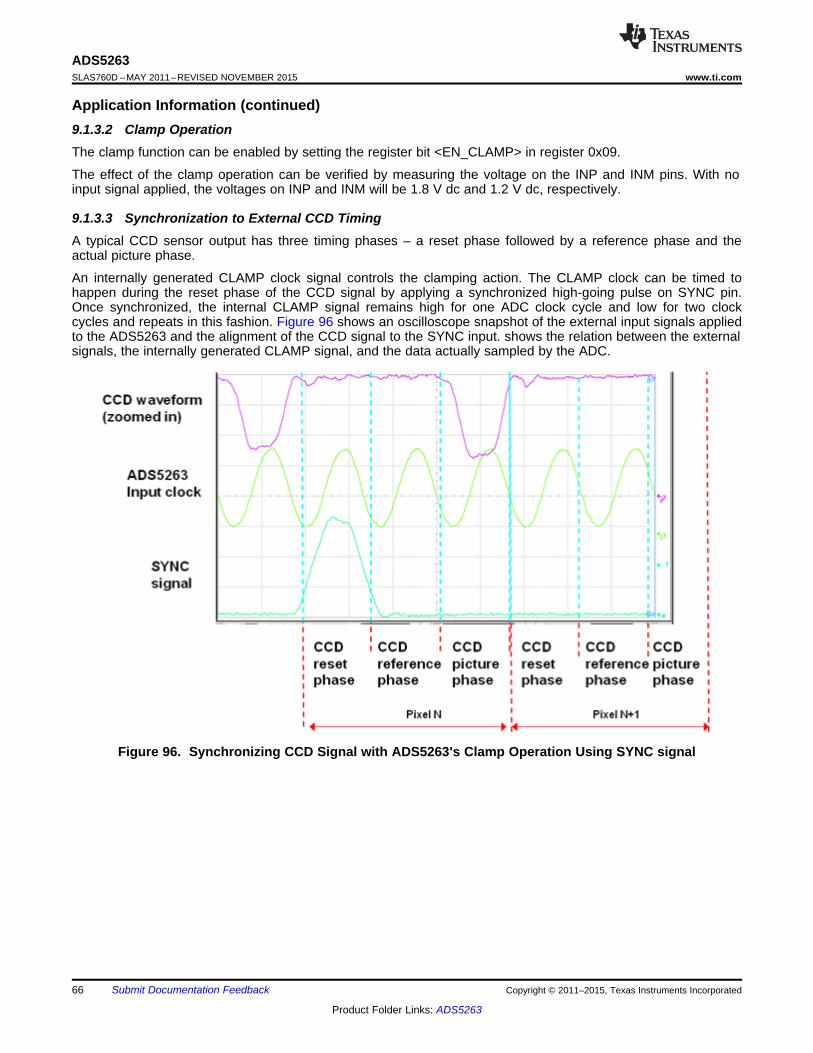
ADS5263SLAS760D –MAY 2011–REVISED NOVEMBER 2015 www.ti.com
Application Information (continued)9.1.3.2 Clamp OperationThe clamp function can be enabled by setting the register bit <EN_CLAMP> in register 0x09.
The effect of the clamp operation can be verified by measuring the voltage on the INP and INM pins. With noinput signal applied, the voltages on INP and INM will be 1.8 V dc and 1.2 V dc, respectively.
9.1.3.3 Synchronization to External CCD TimingA typical CCD sensor output has three timing phases – a reset phase followed by a reference phase and theactual picture phase.
An internally generated CLAMP clock signal controls the clamping action. The CLAMP clock can be timed tohappen during the reset phase of the CCD signal by applying a synchronized high-going pulse on SYNC pin.Once synchronized, the internal CLAMP signal remains high for one ADC clock cycle and low for two clockcycles and repeats in this fashion. Figure 96 shows an oscilloscope snapshot of the external input signals appliedto the ADS5263 and the alignment of the CCD signal to the SYNC input. shows the relation between the externalsignals, the internally generated CLAMP signal, and the data actually sampled by the ADC.
Figure 96. Synchronizing CCD Signal with ADS5263's Clamp Operation Using SYNC signal
66 Submit Documentation Feedback Copyright © 2011–2015, Texas Instruments Incorporated
Product Folder Links: ADS5263
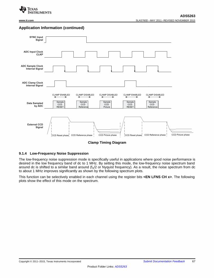
Sample
CCD
RESET
Sample
CCD
Reference
Sample
CCD
Picture
Sample
CCD
RESET
CCD Reset phase CCD Reference phase CCD Picture phase
Sample
CCD
Reference
CCD Reset phase CCD Reference phase CCD Picture phase
CLAMP ENABLED CLAMP DISABLED CLAMP DISABLED CLAMP ENABLED CLAMP DISABLED
ADC Clamp ClockInternal Signal
Data Sampledby ADC
External CCDSignal
ADC Sample ClockInternal Signal
ADC Input ClockCLKP
SYNC InputSignal
ADS5263www.ti.com SLAS760D –MAY 2011–REVISED NOVEMBER 2015
Application Information (continued)
Clamp Timing Diagram
9.1.4 Low-Frequency Noise SuppressionThe low-frequency noise suppression mode is specifically useful in applications where good noise performance isdesired in the low frequency band of dc to 1 MHz. By setting this mode, the low-frequency noise spectrum bandaround dc is shifted to a similar band around (fS/2 or Nyquist frequency). As a result, the noise spectrum from dcto about 1 MHz improves significantly as shown by the following spectrum plots.
This function can be selectively enabled in each channel using the register bits <EN LFNS CH x>. The followingplots show the effect of this mode on the spectrum.
Copyright © 2011–2015, Texas Instruments Incorporated Submit Documentation Feedback 67
Product Folder Links: ADS5263

−140
−130
−120
−110
−100
−90
−80
−70
−60
−50
−40
−30
−20
−10
0
49 49.1 49.2 49.3 49.4 49.5 49.6 49.7 49.8 49.9 50Frequency (MHz)
Am
plitu
de (
dB)
LF Noise Suppression EnabledLF Noise Suppression Disabled
G034
−130
−120
−110
−100
−90
−80
−70
−60
−50
−40
−30
−20
−10
0
0 10 20 30 40 50Frequency (MHz)
Am
plitu
de (
dB)
SFDR = 83.6dBcSNR with Chopper = 91.24dBFSSNR without Chopper = 90.3dBFSTHD = 80.4dBc
G032
−140
−130
−120
−110
−100
−90
−80
−70
−60
−50
−40
−30
−20
−10
0
0 0.1 0.2 0.3 0.4 0.5 0.6 0.7 0.8 0.9 1Frequency (MHz)
Am
plitu
de (
dB)
LF Noise Suppression EnabledLF Noise Suppression Disabled
G033
ADS5263SLAS760D –MAY 2011–REVISED NOVEMBER 2015 www.ti.com
Application Information (continued)
Figure 97. Full-Scale Input Amplitude Figure 98. Spectrum (Zoomed) from DC to 1 MHz
Figure 99. Spectrum (Zoomed) in 1-MHz Band from 49 MHz to 50 MHz (fS=100 MSPS)
9.1.5 External Reference ModeThe ADS5263 supports an external reference mode of operation by applying an input voltage on VCM pin.
As shown in the figure, in this mode, the reference amplifier is still active. Instead of being driven by the internalband-gap voltage, the reference amplifier is driven by the voltage applied on the VCM pin. By driving the VCMpin with a low drift reference, it is possible to improve the reference temperature drift compared to the internalreference mode. The relation between the full-scale voltage of the ADC and the applied voltage on VCM is
Full-scale input voltage = (8/3) x VREFIN
To enable this mode, set the register bits as shown in Table 11. This changes the function of the VCM pin to anexternal reference input pin. The voltage applied on VCM must be 1.5 V ± 50 mV. The current drawn by VCM pinin this mode is around 0.5 mA.
68 Submit Documentation Feedback Copyright © 2011–2015, Texas Instruments Incorporated
Product Folder Links: ADS5263
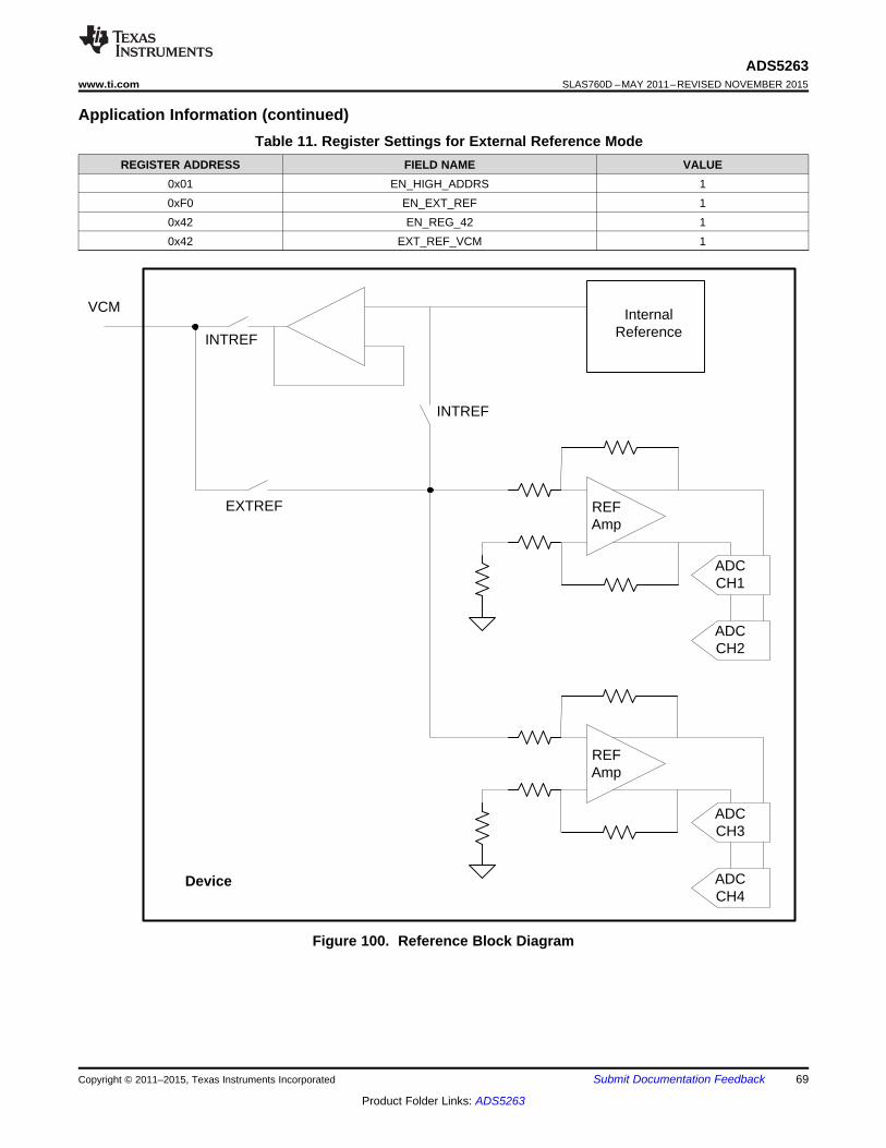
ADCCH4
ADCCH3
REF Amp
ADCCH2
ADCCH1
REF Amp
Internal Reference
INTREF
EXTREF
INTREF
VCM
Device
ADS5263www.ti.com SLAS760D –MAY 2011–REVISED NOVEMBER 2015
Application Information (continued)Table 11. Register Settings for External Reference Mode
REGISTER ADDRESS FIELD NAME VALUE0x01 EN_HIGH_ADDRS 10xF0 EN_EXT_REF 10x42 EN_REG_42 10x42 EXT_REF_VCM 1
Figure 100. Reference Block Diagram
Copyright © 2011–2015, Texas Instruments Incorporated Submit Documentation Feedback 69
Product Folder Links: ADS5263
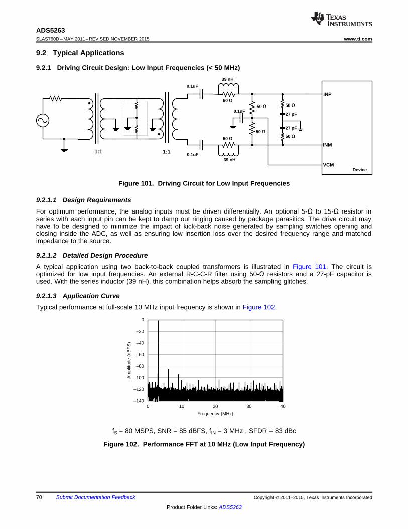
±140
±120
±100
±80
±60
±40
±20
0
0 10 20 30 40
Am
plitu
de (
dBF
S)
Frequency (MHz) C001
INP
INM
VCM
1:1
50
50 0.1uF
1:1
27 pF
50
50
50
50
39 nH
39 nH
0.1uF
0.1uF
Device
27 pF
ADS5263SLAS760D –MAY 2011–REVISED NOVEMBER 2015 www.ti.com
9.2 Typical Applications
9.2.1 Driving Circuit Design: Low Input Frequencies (< 50 MHz)
Figure 101. Driving Circuit for Low Input Frequencies
9.2.1.1 Design RequirementsFor optimum performance, the analog inputs must be driven differentially. An optional 5-Ω to 15-Ω resistor inseries with each input pin can be kept to damp out ringing caused by package parasitics. The drive circuit mayhave to be designed to minimize the impact of kick-back noise generated by sampling switches opening andclosing inside the ADC, as well as ensuring low insertion loss over the desired frequency range and matchedimpedance to the source.
9.2.1.2 Detailed Design ProcedureA typical application using two back-to-back coupled transformers is illustrated in Figure 101. The circuit isoptimized for low input frequencies. An external R-C-C-R filter using 50-Ω resistors and a 27-pF capacitor isused. With the series inductor (39 nH), this combination helps absorb the sampling glitches.
9.2.1.3 Application CurveTypical performance at full-scale 10 MHz input frequency is shown in Figure 102.
fS = 80 MSPS, SNR = 85 dBFS, fIN = 3 MHz , SFDR = 83 dBc
Figure 102. Performance FFT at 10 MHz (Low Input Frequency)
70 Submit Documentation Feedback Copyright © 2011–2015, Texas Instruments Incorporated
Product Folder Links: ADS5263

±125
±100
±75
±50
±25
0
0 5 10 15 20 25 30 35 40
Am
plitu
de (
dBF
S)
Frequency (MHz) C004
INP
INM
VCM
1:1
100
100 0.1uF
1:1
10 pF
50
50
0.1uF
0.1uF
Device
10 pF
ADS5263www.ti.com SLAS760D –MAY 2011–REVISED NOVEMBER 2015
Typical Applications (continued)9.2.2 Driving Circuit Design: Input Frequencies > 50 MHz
Figure 103. Driving Circuit for High Input Frequencies (fIN > 50 MHz)
9.2.2.1 Design RequirementsTo achieve optimum performance at high input frequencies, an example driving circuit is shown in Figure 103.
9.2.2.2 Detailed Design ProcedureWhen input frequencies are greater than 50 MHz, series inductance from low frequency driving circuit should beremoved so as not limit the signal bandwidth. The corner frequency of R-C-C-R low pass filter should also bechanged to suit the input frequency.
9.2.2.3 Application CurveFigure 104 shows the performance obtained by using the circuit shown in Figure 104.
fS = 80 MSPS, SNR = 78.2 dBFS, fIN = 65 MHz, SFDR = 75 dBc
Figure 104. Performance FFT at 65 MHz
10 Power Supply RecommendationsThe device requires 3.3-V for Analog Supply (AVDD) and 1.8-V for Digital Supply (LVDD). There is no specificsequence required to bring-up the power-supplies. AVDD and LVDD can power up in any order.
Copyright © 2011–2015, Texas Instruments Incorporated Submit Documentation Feedback 71
Product Folder Links: ADS5263
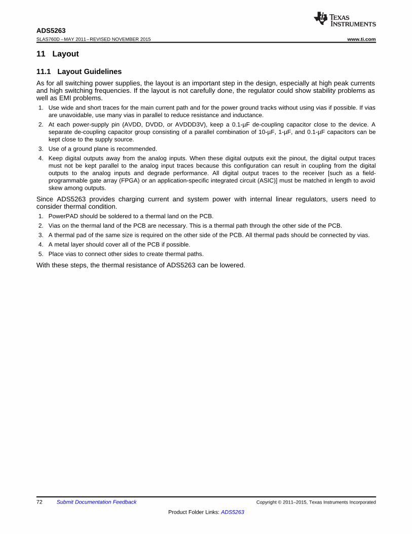
ADS5263SLAS760D –MAY 2011–REVISED NOVEMBER 2015 www.ti.com
11 Layout
11.1 Layout GuidelinesAs for all switching power supplies, the layout is an important step in the design, especially at high peak currentsand high switching frequencies. If the layout is not carefully done, the regulator could show stability problems aswell as EMI problems.1. Use wide and short traces for the main current path and for the power ground tracks without using vias if possible. If vias
are unavoidable, use many vias in parallel to reduce resistance and inductance.2. At each power-supply pin (AVDD, DVDD, or AVDDD3V), keep a 0.1-µF de-coupling capacitor close to the device. A
separate de-coupling capacitor group consisting of a parallel combination of 10-µF, 1-µF, and 0.1-µF capacitors can bekept close to the supply source.
3. Use of a ground plane is recommended.4. Keep digital outputs away from the analog inputs. When these digital outputs exit the pinout, the digital output traces
must not be kept parallel to the analog input traces because this configuration can result in coupling from the digitaloutputs to the analog inputs and degrade performance. All digital output traces to the receiver [such as a field-programmable gate array (FPGA) or an application-specific integrated circuit (ASIC)] must be matched in length to avoidskew among outputs.
Since ADS5263 provides charging current and system power with internal linear regulators, users need toconsider thermal condition.1. PowerPAD should be soldered to a thermal land on the PCB.2. Vias on the thermal land of the PCB are necessary. This is a thermal path through the other side of the PCB.3. A thermal pad of the same size is required on the other side of the PCB. All thermal pads should be connected by vias.4. A metal layer should cover all of the PCB if possible.5. Place vias to connect other sides to create thermal paths.
With these steps, the thermal resistance of ADS5263 can be lowered.
72 Submit Documentation Feedback Copyright © 2011–2015, Texas Instruments Incorporated
Product Folder Links: ADS5263
ADS5263www.ti.com SLAS760D –MAY 2011–REVISED NOVEMBER 2015
11.2 Layout Example
Figure 105. Layout of Board
Copyright © 2011–2015, Texas Instruments Incorporated Submit Documentation Feedback 73
Product Folder Links: ADS5263

10 S
N D
PSINAD = 10Log
P + P
10 S
N
PSNR = 10Log
P
ADS5263SLAS760D –MAY 2011–REVISED NOVEMBER 2015 www.ti.com
12 Device and Documentation Support
12.1 Device Support
12.1.1 Definition of Specifications
Analog Bandwidth – The analog input frequency at which the power of the fundamental is reduced by 3 dB withrespect to the low-frequency value.
Aperture Delay – The delay in time between the rising edge of the input sampling clock and the actual time atwhich the sampling occurs. This delay is different across channels. The maximum variation is specified asaperture delay variation (channel-to-channel).
Aperture Uncertainty (Jitter) – The sample-to-sample variation in aperture delay.
Clock Pulse Width/Duty Cycle – The duty cycle of a clock signal is the ratio of the time the clock signal remainsat a logic high (clock pulse width) to the period of the clock signal. Duty cycle is typically expressed as apercentage. A perfect differential sine-wave clock results in a 50% duty cycle.
Maximum Conversion Rate – The maximum sampling rate at which specified operation is given. All parametrictesting is performed at this sampling rate unless otherwise noted.
Minimum Conversion Rate – The minimum sampling rate at which the ADC functions.
Differential Nonlinearity (DNL) – An ideal ADC exhibits code transitions at analog input values spaced exactly1 LSB apart. The DNL is the deviation of any single step from this ideal value, measured in units of LSBs.
Integral Nonlinearity (INL) – The INL is the deviation of the ADC transfer function from a best fit line determinedby a least squares curve fit of that transfer function, measured in units of LSBs.
Gain Error – Gain error is the deviation of the ADC actual input full-scale range from its ideal value. The gainerror is given as a percentage of the ideal input full-scale range. Gain error has two components: error as aresult of reference inaccuracy and error as a result of the channel. Both errors are specified independently asEGREF and EGCHAN.
To a first-order approximation, the total gain error is ETOTAL ~ EGREF + EGCHAN.
For example, if ETOTAL = ±0.5%, the full-scale input varies from (1 – 0.5/100) x FSideal to (1 + 0.5/100) x FSideal.
Offset Error – The offset error is the difference, given in number of LSBs, between the ADC actual average idlechannel output code and the ideal average idle channel output code. This quantity is often mapped into millivolts.
Temperature Drift – The temperature drift coefficient (with respect to gain error and offset error) specifies thechange per degree Celsius of the parameter from TMIN to TMAX. It is calculated by dividing the maximum deviationof the parameter across the TMIN to TMAX range by the difference TMAX – TMIN.
Signal-to-Noise Ratio – SNR is the ratio of the power of the fundamental (PS) to the noise floor power (PN),excluding the power at dc and the first nine harmonics.
(1)
SNR is either given in units of dBc (dB to carrier) when the absolute power of the fundamental is used as thereference, or dBFS (dB to full-scale) when the power of the fundamental is extrapolated to the converter full-scale range.
Signal-to-Noise and Distortion (SINAD) – SINAD is the ratio of the power of the fundamental (PS) to the powerof all the other spectral components including noise (PN) and distortion (PD), but excluding dc.
(2)
SINAD is either given in units of dBc (dB to carrier) when the absolute power of the fundamental is used as thereference, or dBFS (dB to full-scale) when the power of the fundamental is extrapolated to the converter full-scale range.
74 Submit Documentation Feedback Copyright © 2011–2015, Texas Instruments Incorporated
Product Folder Links: ADS5263

(Expressed in dBc)DVCM
DVOUT10CMRR = 20Log
(Expressed in dBc)DVSUP
DVOUT10PSRR = 20Log
10 S
N
PTHD = 10Log
P
SINAD 1.76ENOB =
6.02
-
ADS5263www.ti.com SLAS760D –MAY 2011–REVISED NOVEMBER 2015
Device Support (continued)Effective Number of Bits (ENOB) – ENOB is a measure of the converter performance as compared to thetheoretical limit based on quantization noise.
(3)
Total Harmonic Distortion (THD) – THD is the ratio of the power of the fundamental (PS) to the power of thefirst nine harmonics (PD).
(4)
THD is typically given in units of dBc (dB to carrier).
Spurious-Free Dynamic Range (SFDR) – The ratio of the power of the fundamental to the highest otherspectral component (either spur or harmonic). SFDR is typically given in units of dBc (dB to carrier).
Two-Tone Intermodulation Distortion – IMD3 is the ratio of the power of the fundamental (at frequencies f1and f2) to the power of the worst spectral component at either frequency 2f1 – f2 or 2f2 – f1. IMD3 is either givenin units of dBc (dB to carrier) when the absolute power of the fundamental is used as the reference, or dBFS (dBto full-scale) when the power of the fundamental is extrapolated to the converter full-scale range.
DC Power-Supply Rejection Ratio (DC PSRR) – DC PSSR is the ratio of the change in offset error to a changein analog supply voltage. The dc PSRR is typically given in units of mV/V.
AC Power-Supply Rejection Ratio (AC PSRR) – AC PSRR is the measure of rejection of variations in thesupply voltage by the ADC. If ΔVSUP is the change in supply voltage and ΔVOUT is the resultant change of theADC output code (referred to the input), then:
(5)
Voltage Overload Recovery – The number of clock cycles taken to recover to less than 1% error after anoverload on the analog inputs. This is tested by separately applying a sine wave signal with 6dB positive andnegative overload. The deviation of the first few samples after the overload (from the expected values) is noted.
Common-Mode Rejection Ratio (CMRR) – CMRR is the measure of rejection of variation in the analog inputcommon-mode by the ADC. If ΔVCM_IN is the change in the common-mode voltage of the input pins and ΔVOUT isthe resulting change of the ADC output code (referred to the input), then:
(6)
Crosstalk (only for multi-channel ADCs) – This is a measure of the internal coupling of a signal from anadjacent channel into the channel of interest. It is specified separately for coupling from the immediateneighboring channel (near-channel) and for coupling from channel across the package (far-channel). It is usuallymeasured by applying a full-scale signal in the adjacent channel. Crosstalk is the ratio of the power of thecoupling signal (as measured at the output of the channel of interest) to the power of the signal applied at theadjacent channel input. It is typically expressed in dBc.
12.2 Community ResourcesThe following links connect to TI community resources. Linked contents are provided "AS IS" by the respectivecontributors. They do not constitute TI specifications and do not necessarily reflect TI's views; see TI's Terms ofUse.
TI E2E™ Online Community TI's Engineer-to-Engineer (E2E) Community. Created to foster collaborationamong engineers. At e2e.ti.com, you can ask questions, share knowledge, explore ideas and helpsolve problems with fellow engineers.
Design Support TI's Design Support Quickly find helpful E2E forums along with design support tools andcontact information for technical support.
Copyright © 2011–2015, Texas Instruments Incorporated Submit Documentation Feedback 75
Product Folder Links: ADS5263
ADS5263SLAS760D –MAY 2011–REVISED NOVEMBER 2015 www.ti.com
12.3 TrademarksE2E is a trademark of Texas Instruments.All other trademarks are the property of their respective owners.
12.4 Electrostatic Discharge CautionThese devices have limited built-in ESD protection. The leads should be shorted together or the device placed in conductive foamduring storage or handling to prevent electrostatic damage to the MOS gates.
12.5 GlossarySLYZ022 — TI Glossary.
This glossary lists and explains terms, acronyms, and definitions.
13 Mechanical, Packaging, and Orderable InformationThe following pages include mechanical, packaging, and orderable information. This information is the mostcurrent data available for the designated devices. This data is subject to change without notice and revision ofthis document. For browser-based versions of this data sheet, refer to the left-hand navigation.
13.1 Packaging
13.1.1 Exposed PadThe exposed pad at the bottom of the package is the main path for heat dissipation. Therefore, the pad must besoldered to a ground plane on the PCB for best thermal performance. The pad must be connected to the groundplane through the optimum number of vias.
For detailed information, see application notes QFN Layout Guidelines (SLOA122) and QFN/SON PCBAttachment (SLUA271), both available for download at the TI web site (www.ti.com). One can also visit TI’sthermal website at www.ti.com/thermal.
13.1.2 Non-Magnetic PackageAn important requirement in magnetic resonance imaging (MRI) applications is the magnetic compatibility ofcomponents mounted close to the RF coil area. Any ferromagnetic material in the component packageintroduces an artifact in the MRI image. Therefore, it is preferred to have components with non-magneticpackages.
The ADS5263 is available in a special non-magnetic package that does not create any image artifacts, even inthe presence of high magnetic fields. The non-magnetic part is orderable with the suffix “-NM”.
76 Submit Documentation Feedback Copyright © 2011–2015, Texas Instruments Incorporated
Product Folder Links: ADS5263

PACKAGE OPTION ADDENDUM
www.ti.com 4-Sep-2015
Addendum-Page 1
PACKAGING INFORMATION
Orderable Device Status(1)
Package Type PackageDrawing
Pins PackageQty
Eco Plan(2)
Lead/Ball Finish(6)
MSL Peak Temp(3)
Op Temp (°C) Device Marking(4/5)
Samples
ADS5263IRGCR ACTIVE VQFN RGC 64 2000 Green (RoHS& no Sb/Br)
CU SN Level-3-260C-168 HR -40 to 85 ADS5263
ADS5263IRGCR-NM ACTIVE VQFN RGC 64 2000 Green (RoHS& no Sb/Br)
CU SN Level-3-260C-168 HR -40 to 85 ADS5263NM
ADS5263IRGCT ACTIVE VQFN RGC 64 250 Green (RoHS& no Sb/Br)
CU SN Level-3-260C-168 HR -40 to 85 ADS5263
ADS5263IRGCT-NM ACTIVE VQFN RGC 64 250 Green (RoHS& no Sb/Br)
CU SN Level-3-260C-168 HR -40 to 85 ADS5263NM
(1) The marketing status values are defined as follows:ACTIVE: Product device recommended for new designs.LIFEBUY: TI has announced that the device will be discontinued, and a lifetime-buy period is in effect.NRND: Not recommended for new designs. Device is in production to support existing customers, but TI does not recommend using this part in a new design.PREVIEW: Device has been announced but is not in production. Samples may or may not be available.OBSOLETE: TI has discontinued the production of the device.
(2) Eco Plan - The planned eco-friendly classification: Pb-Free (RoHS), Pb-Free (RoHS Exempt), or Green (RoHS & no Sb/Br) - please check http://www.ti.com/productcontent for the latest availabilityinformation and additional product content details.TBD: The Pb-Free/Green conversion plan has not been defined.Pb-Free (RoHS): TI's terms "Lead-Free" or "Pb-Free" mean semiconductor products that are compatible with the current RoHS requirements for all 6 substances, including the requirement thatlead not exceed 0.1% by weight in homogeneous materials. Where designed to be soldered at high temperatures, TI Pb-Free products are suitable for use in specified lead-free processes.Pb-Free (RoHS Exempt): This component has a RoHS exemption for either 1) lead-based flip-chip solder bumps used between the die and package, or 2) lead-based die adhesive used betweenthe die and leadframe. The component is otherwise considered Pb-Free (RoHS compatible) as defined above.Green (RoHS & no Sb/Br): TI defines "Green" to mean Pb-Free (RoHS compatible), and free of Bromine (Br) and Antimony (Sb) based flame retardants (Br or Sb do not exceed 0.1% by weightin homogeneous material)
(3) MSL, Peak Temp. - The Moisture Sensitivity Level rating according to the JEDEC industry standard classifications, and peak solder temperature.
(4) There may be additional marking, which relates to the logo, the lot trace code information, or the environmental category on the device.
(5) Multiple Device Markings will be inside parentheses. Only one Device Marking contained in parentheses and separated by a "~" will appear on a device. If a line is indented then it is a continuationof the previous line and the two combined represent the entire Device Marking for that device.
(6) Lead/Ball Finish - Orderable Devices may have multiple material finish options. Finish options are separated by a vertical ruled line. Lead/Ball Finish values may wrap to two lines if the finishvalue exceeds the maximum column width.

PACKAGE OPTION ADDENDUM
www.ti.com 4-Sep-2015
Addendum-Page 2
Important Information and Disclaimer:The information provided on this page represents TI's knowledge and belief as of the date that it is provided. TI bases its knowledge and belief on informationprovided by third parties, and makes no representation or warranty as to the accuracy of such information. Efforts are underway to better integrate information from third parties. TI has taken andcontinues to take reasonable steps to provide representative and accurate information but may not have conducted destructive testing or chemical analysis on incoming materials and chemicals.TI and TI suppliers consider certain information to be proprietary, and thus CAS numbers and other limited information may not be available for release.
In no event shall TI's liability arising out of such information exceed the total purchase price of the TI part(s) at issue in this document sold by TI to Customer on an annual basis.
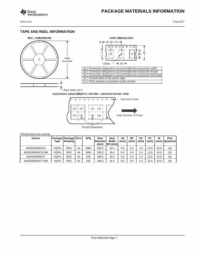
TAPE AND REEL INFORMATION
*All dimensions are nominal
Device PackageType
PackageDrawing
Pins SPQ ReelDiameter
(mm)
ReelWidth
W1 (mm)
A0(mm)
B0(mm)
K0(mm)
P1(mm)
W(mm)
Pin1Quadrant
ADS5263IRGCR VQFN RGC 64 2000 330.0 16.4 9.3 9.3 1.5 12.0 16.0 Q2
ADS5263IRGCR-NM VQFN RGC 64 2000 330.0 16.4 9.3 9.3 1.5 12.0 16.0 Q2
ADS5263IRGCT VQFN RGC 64 250 180.0 16.4 9.3 9.3 1.5 12.0 16.0 Q2
ADS5263IRGCT-NM VQFN RGC 64 250 180.0 16.4 9.3 9.3 1.5 12.0 16.0 Q2
PACKAGE MATERIALS INFORMATION
www.ti.com 3-Aug-2017
Pack Materials-Page 1

*All dimensions are nominal
Device Package Type Package Drawing Pins SPQ Length (mm) Width (mm) Height (mm)
ADS5263IRGCR VQFN RGC 64 2000 336.6 336.6 28.6
ADS5263IRGCR-NM VQFN RGC 64 2000 336.6 336.6 28.6
ADS5263IRGCT VQFN RGC 64 250 213.0 191.0 55.0
ADS5263IRGCT-NM VQFN RGC 64 250 213.0 191.0 55.0
PACKAGE MATERIALS INFORMATION
www.ti.com 3-Aug-2017
Pack Materials-Page 2
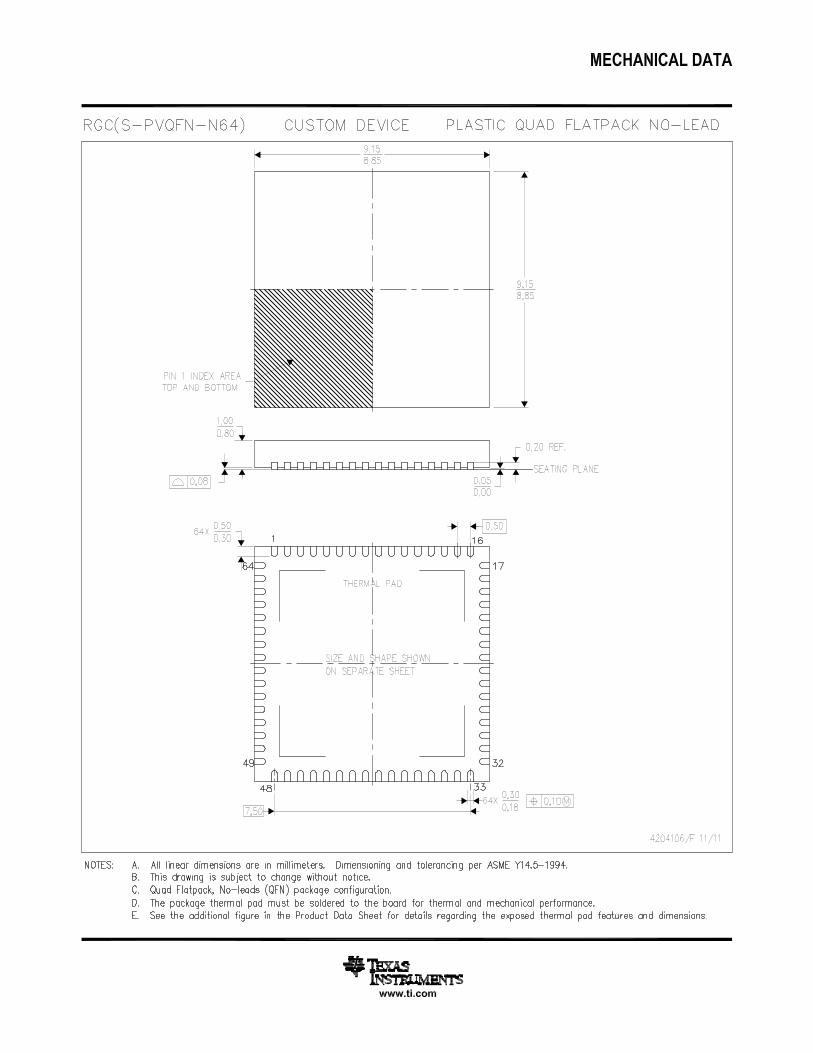
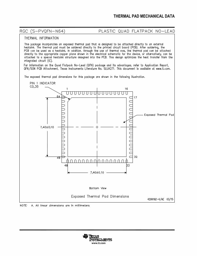
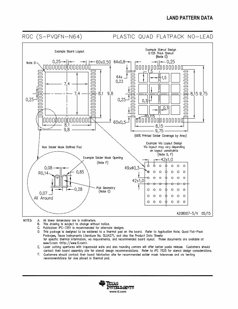
IMPORTANT NOTICE
Texas Instruments Incorporated (TI) reserves the right to make corrections, enhancements, improvements and other changes to itssemiconductor products and services per JESD46, latest issue, and to discontinue any product or service per JESD48, latest issue. Buyersshould obtain the latest relevant information before placing orders and should verify that such information is current and complete.TI’s published terms of sale for semiconductor products (http://www.ti.com/sc/docs/stdterms.htm) apply to the sale of packaged integratedcircuit products that TI has qualified and released to market. Additional terms may apply to the use or sale of other types of TI products andservices.Reproduction of significant portions of TI information in TI data sheets is permissible only if reproduction is without alteration and isaccompanied by all associated warranties, conditions, limitations, and notices. TI is not responsible or liable for such reproduceddocumentation. Information of third parties may be subject to additional restrictions. Resale of TI products or services with statementsdifferent from or beyond the parameters stated by TI for that product or service voids all express and any implied warranties for theassociated TI product or service and is an unfair and deceptive business practice. TI is not responsible or liable for any such statements.Buyers and others who are developing systems that incorporate TI products (collectively, “Designers”) understand and agree that Designersremain responsible for using their independent analysis, evaluation and judgment in designing their applications and that Designers havefull and exclusive responsibility to assure the safety of Designers' applications and compliance of their applications (and of all TI productsused in or for Designers’ applications) with all applicable regulations, laws and other applicable requirements. Designer represents that, withrespect to their applications, Designer has all the necessary expertise to create and implement safeguards that (1) anticipate dangerousconsequences of failures, (2) monitor failures and their consequences, and (3) lessen the likelihood of failures that might cause harm andtake appropriate actions. Designer agrees that prior to using or distributing any applications that include TI products, Designer willthoroughly test such applications and the functionality of such TI products as used in such applications.TI’s provision of technical, application or other design advice, quality characterization, reliability data or other services or information,including, but not limited to, reference designs and materials relating to evaluation modules, (collectively, “TI Resources”) are intended toassist designers who are developing applications that incorporate TI products; by downloading, accessing or using TI Resources in anyway, Designer (individually or, if Designer is acting on behalf of a company, Designer’s company) agrees to use any particular TI Resourcesolely for this purpose and subject to the terms of this Notice.TI’s provision of TI Resources does not expand or otherwise alter TI’s applicable published warranties or warranty disclaimers for TIproducts, and no additional obligations or liabilities arise from TI providing such TI Resources. TI reserves the right to make corrections,enhancements, improvements and other changes to its TI Resources. TI has not conducted any testing other than that specificallydescribed in the published documentation for a particular TI Resource.Designer is authorized to use, copy and modify any individual TI Resource only in connection with the development of applications thatinclude the TI product(s) identified in such TI Resource. NO OTHER LICENSE, EXPRESS OR IMPLIED, BY ESTOPPEL OR OTHERWISETO ANY OTHER TI INTELLECTUAL PROPERTY RIGHT, AND NO LICENSE TO ANY TECHNOLOGY OR INTELLECTUAL PROPERTYRIGHT OF TI OR ANY THIRD PARTY IS GRANTED HEREIN, including but not limited to any patent right, copyright, mask work right, orother intellectual property right relating to any combination, machine, or process in which TI products or services are used. Informationregarding or referencing third-party products or services does not constitute a license to use such products or services, or a warranty orendorsement thereof. Use of TI Resources may require a license from a third party under the patents or other intellectual property of thethird party, or a license from TI under the patents or other intellectual property of TI.TI RESOURCES ARE PROVIDED “AS IS” AND WITH ALL FAULTS. TI DISCLAIMS ALL OTHER WARRANTIES ORREPRESENTATIONS, EXPRESS OR IMPLIED, REGARDING RESOURCES OR USE THEREOF, INCLUDING BUT NOT LIMITED TOACCURACY OR COMPLETENESS, TITLE, ANY EPIDEMIC FAILURE WARRANTY AND ANY IMPLIED WARRANTIES OFMERCHANTABILITY, FITNESS FOR A PARTICULAR PURPOSE, AND NON-INFRINGEMENT OF ANY THIRD PARTY INTELLECTUALPROPERTY RIGHTS. TI SHALL NOT BE LIABLE FOR AND SHALL NOT DEFEND OR INDEMNIFY DESIGNER AGAINST ANY CLAIM,INCLUDING BUT NOT LIMITED TO ANY INFRINGEMENT CLAIM THAT RELATES TO OR IS BASED ON ANY COMBINATION OFPRODUCTS EVEN IF DESCRIBED IN TI RESOURCES OR OTHERWISE. IN NO EVENT SHALL TI BE LIABLE FOR ANY ACTUAL,DIRECT, SPECIAL, COLLATERAL, INDIRECT, PUNITIVE, INCIDENTAL, CONSEQUENTIAL OR EXEMPLARY DAMAGES INCONNECTION WITH OR ARISING OUT OF TI RESOURCES OR USE THEREOF, AND REGARDLESS OF WHETHER TI HAS BEENADVISED OF THE POSSIBILITY OF SUCH DAMAGES.Unless TI has explicitly designated an individual product as meeting the requirements of a particular industry standard (e.g., ISO/TS 16949and ISO 26262), TI is not responsible for any failure to meet such industry standard requirements.Where TI specifically promotes products as facilitating functional safety or as compliant with industry functional safety standards, suchproducts are intended to help enable customers to design and create their own applications that meet applicable functional safety standardsand requirements. Using products in an application does not by itself establish any safety features in the application. Designers mustensure compliance with safety-related requirements and standards applicable to their applications. Designer may not use any TI products inlife-critical medical equipment unless authorized officers of the parties have executed a special contract specifically governing such use.Life-critical medical equipment is medical equipment where failure of such equipment would cause serious bodily injury or death (e.g., lifesupport, pacemakers, defibrillators, heart pumps, neurostimulators, and implantables). Such equipment includes, without limitation, allmedical devices identified by the U.S. Food and Drug Administration as Class III devices and equivalent classifications outside the U.S.TI may expressly designate certain products as completing a particular qualification (e.g., Q100, Military Grade, or Enhanced Product).Designers agree that it has the necessary expertise to select the product with the appropriate qualification designation for their applicationsand that proper product selection is at Designers’ own risk. Designers are solely responsible for compliance with all legal and regulatoryrequirements in connection with such selection.Designer will fully indemnify TI and its representatives against any damages, costs, losses, and/or liabilities arising out of Designer’s non-compliance with the terms and provisions of this Notice.
Mailing Address: Texas Instruments, Post Office Box 655303, Dallas, Texas 75265Copyright © 2017, Texas Instruments Incorporated
Related Documents