Abrupt heating-induced high-quality crystalline rubrene thin films for organic thin-film transistors Hyeok Moo Lee a , Hanul Moon b , Hyo-Sik Kim a , Yong Nam Kim a , Sung-Min Choi a , Seunghyup Yoo b , Sung Oh Cho a,⇑ a Department of Nuclear and Quantum Engineering, Korea Advanced Institute of Science and Technology, Daejeon 305-701, Republic of Korea b Department of Electrical Engineering, Korea Advanced Institute of Science and Technology, Daejeon 305-701, Republic of Korea article info Article history: Received 24 March 2011 Received in revised form 16 May 2011 Accepted 17 May 2011 Available online 31 May 2011 Keywords: Organic thin-film transistors (OTFTs) Rubrene High-quality crystalline film Organic semiconductor active layer abstract We present a simple but effective approach to fabricate high-quality crystalline rubrene thin-film active layers for organic thin-film transistors (OTFTs) based on an abrupt heating process. Through this method, continuous, highly ordered, and highly oriented crystalline rubrene thin films comprising large single-crystalline grains (average size: 80 lm) can be remarkably rapidly produced in just 1 min without any dielectric surface modification pro- cess. OTFTs with carrier mobility as high as 1.21 cm 2 V 1 s 1 and on/off current ratios greater than 10 6 are demonstrated under air-ambient condition using the approach. These results suggest that our approach is very promising to fabricate high-performance OTFTs for practical applications in organic electronics. Ó 2011 Elsevier B.V. All rights reserved. 1. Introduction During the last decade, organic field-effect transistors (OFETs) with mobilities comparable to those of hydroge- nated amorphous silicon (a-Si:H) FET have attracted much attention for their practical applications in active-matrix displays [1,2], radio frequency identification tags [3–5], smart cards [6], and sensors [7,8]. The performance of OFETs is strongly influenced by the quality of active layers including crystallinity, grain size, molecular orientation and grain interconnection [9,10]. From this point of view, OFETs based on organic single crystals which may be con- sidered as ideal exhibit the outstanding device perfor- mance [11–14]; for example, mobility values as high as 15–40 cm 2 V 1 s 1 have been demonstrated in rubrene single-crystal FETs. However, difficulties in large-area fab- rication of organic single crystals act as a major obstacle in the practical application of organic single-crystal transis- tors. In this respect, a majority of the research was concen- trated on OFETs using polycrystalline thin-film active layers, or, organic thin-film transistors (OTFTs), which are better positioned in such processing issues. Among the organic semiconductors, rubrene shows highest carrier mobility in the form of single-crystal transis- tor. However, rubrene TFTs prepared by conventional fabri- cation routes did not exhibit superior carrier mobilities because of difficulty in achieving highly-quality crystalline rubrene active layer [15–17]. For instance, OTFTs based on polycrystalline rubrene spherulite structures grown by pos- tannealing method demonstrate very low mobilities about 10 4 cm 2 V 1 s 1 [17]. To date, a few methods to improve the crystallinity of rubrene films such as ‘‘hot wall’’ deposi- tion [18], slowly ramping substrate temperature during vacuum deposition [19], and template induced crystalliza- tion [20] have been developed. The rubrene TFTs in these studies exhibit relatively high performance characteristics. Nevertheless, such efforts typically involve self-assembled monolayer (SAM) treatment that modifies the surface of dielectrics so that it can be compatible with the crystalline growth of rubrene films. The SAM treatment adds to a pro- cessing complexity and thus it would be better if they can be avoided. Stingelin-Stutzmann et al. [21] reported OTFT based on solution-processed rubrene hypereutectics and 1566-1199/$ - see front matter Ó 2011 Elsevier B.V. All rights reserved. doi:10.1016/j.orgel.2011.05.015 ⇑ Corresponding author. Tel.: +82 42 350 3823; fax: +82 42 350 3810. E-mail address: [email protected] (S.O. Cho). Organic Electronics 12 (2011) 1446–1453 Contents lists available at ScienceDirect Organic Electronics journal homepage: www.elsevier.com/locate/orgel

Welcome message from author
This document is posted to help you gain knowledge. Please leave a comment to let me know what you think about it! Share it to your friends and learn new things together.
Transcript
Organic Electronics 12 (2011) 1446–1453
Contents lists available at ScienceDirect
Organic Electronics
journal homepage: www.elsevier .com/locate /orgel
Abrupt heating-induced high-quality crystalline rubrene thin filmsfor organic thin-film transistors
Hyeok Moo Lee a, Hanul Moon b, Hyo-Sik Kim a, Yong Nam Kim a, Sung-Min Choi a,Seunghyup Yoo b, Sung Oh Cho a,⇑a Department of Nuclear and Quantum Engineering, Korea Advanced Institute of Science and Technology, Daejeon 305-701, Republic of Koreab Department of Electrical Engineering, Korea Advanced Institute of Science and Technology, Daejeon 305-701, Republic of Korea
a r t i c l e i n f o
Article history:Received 24 March 2011Received in revised form 16 May 2011Accepted 17 May 2011Available online 31 May 2011
Keywords:Organic thin-film transistors (OTFTs)RubreneHigh-quality crystalline filmOrganic semiconductor active layer
1566-1199/$ - see front matter � 2011 Elsevier B.Vdoi:10.1016/j.orgel.2011.05.015
⇑ Corresponding author. Tel.: +82 42 350 3823; faE-mail address: [email protected] (S.O. Cho).
a b s t r a c t
We present a simple but effective approach to fabricate high-quality crystalline rubrenethin-film active layers for organic thin-film transistors (OTFTs) based on an abrupt heatingprocess. Through this method, continuous, highly ordered, and highly oriented crystallinerubrene thin films comprising large single-crystalline grains (average size: �80 lm) can beremarkably rapidly produced in just 1 min without any dielectric surface modification pro-cess. OTFTs with carrier mobility as high as 1.21 cm2 V�1 s�1 and on/off current ratiosgreater than 106 are demonstrated under air-ambient condition using the approach. Theseresults suggest that our approach is very promising to fabricate high-performance OTFTsfor practical applications in organic electronics.
� 2011 Elsevier B.V. All rights reserved.
1. Introduction
During the last decade, organic field-effect transistors(OFETs) with mobilities comparable to those of hydroge-nated amorphous silicon (a-Si:H) FET have attracted muchattention for their practical applications in active-matrixdisplays [1,2], radio frequency identification tags [3–5],smart cards [6], and sensors [7,8]. The performance ofOFETs is strongly influenced by the quality of active layersincluding crystallinity, grain size, molecular orientationand grain interconnection [9,10]. From this point of view,OFETs based on organic single crystals which may be con-sidered as ideal exhibit the outstanding device perfor-mance [11–14]; for example, mobility values as high as15–40 cm2 V�1 s�1 have been demonstrated in rubrenesingle-crystal FETs. However, difficulties in large-area fab-rication of organic single crystals act as a major obstacle inthe practical application of organic single-crystal transis-tors. In this respect, a majority of the research was concen-trated on OFETs using polycrystalline thin-film active
. All rights reserved.
x: +82 42 350 3810.
layers, or, organic thin-film transistors (OTFTs), which arebetter positioned in such processing issues.
Among the organic semiconductors, rubrene showshighest carrier mobility in the form of single-crystal transis-tor. However, rubrene TFTs prepared by conventional fabri-cation routes did not exhibit superior carrier mobilitiesbecause of difficulty in achieving highly-quality crystallinerubrene active layer [15–17]. For instance, OTFTs based onpolycrystalline rubrene spherulite structures grown by pos-tannealing method demonstrate very low mobilities about10�4 cm2 V�1 s�1 [17]. To date, a few methods to improvethe crystallinity of rubrene films such as ‘‘hot wall’’ deposi-tion [18], slowly ramping substrate temperature duringvacuum deposition [19], and template induced crystalliza-tion [20] have been developed. The rubrene TFTs in thesestudies exhibit relatively high performance characteristics.Nevertheless, such efforts typically involve self-assembledmonolayer (SAM) treatment that modifies the surface ofdielectrics so that it can be compatible with the crystallinegrowth of rubrene films. The SAM treatment adds to a pro-cessing complexity and thus it would be better if they can beavoided. Stingelin-Stutzmann et al. [21] reported OTFTbased on solution-processed rubrene hypereutectics and
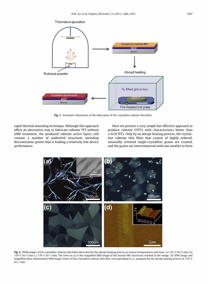
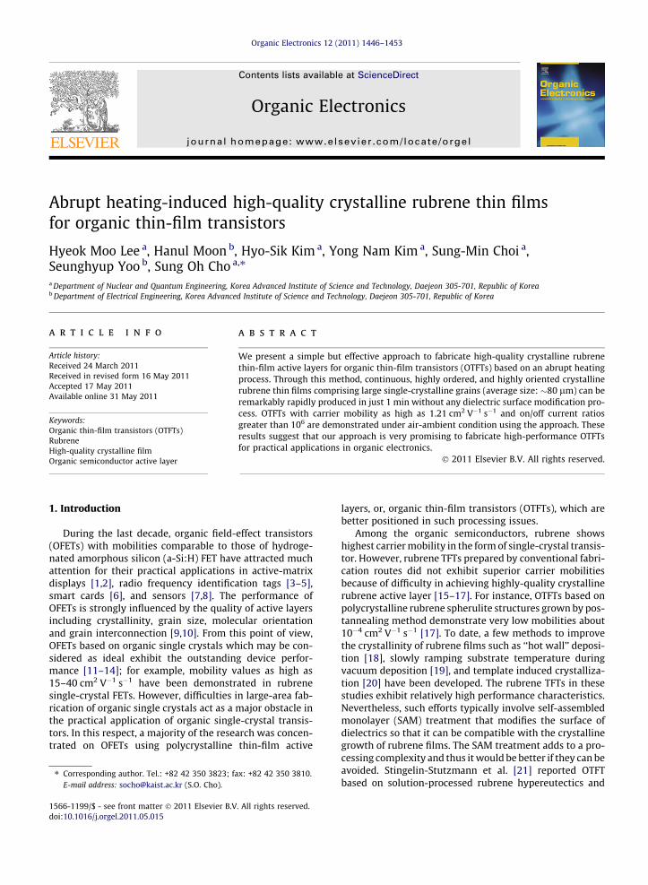
Fig. 1. Schematic illustration of the fabrication of the crystalline rubrene thin films.
H.M. Lee et al. / Organic Electronics 12 (2011) 1446–1453 1447
rapid thermal annealing technique. Although this approachoffers an alternative way to fabricate rubrene TFT withoutSAM treatment, the produced rubrene active layers stillcontain a number of undesired structures includingdiscontinuous grains that is leading a relatively low deviceperformance.
Fig. 2. POM images of the crystalline rubrene thin films fabricated by the abrupt150 �C for 5 min (c) 170 �C for 1 min. The inset in (a) is the magnified SEM imagmagnified three-dimensional AFM image (inset) of the crystalline rubrene thin fifor 1 min.
Here we present a very simple but effective approach toproduce rubrene OTFTs with characteristics better thana-Si:H TFTs. Only by an abrupt heating process, the crystal-line rubrene thin films that consist of highly ordered,uniaxially oriented single-crystalline grains are created,and the grains are interconnected with one another to form
heating process at various temperatures and time: (a) 125 �C for 5 min, (b)e of the branch-like structures marked in the image. (d) AFM image and
lm, corresponding to (c), prepared by the abrupt heating process at 170 �C
1448 H.M. Lee et al. / Organic Electronics 12 (2011) 1446–1453
continuous films over the whole dielectric surfaces. Suchhigh-quality crystalline rubrene thin films are remarkablyrapidly produced in 1 min through this approach. More-over, the approach does not require any surface modifica-tion of gate dielectrics of OTFTs, which is generallyindispensable in the other methods developed to date forenhancing the performance of OTFTs.
2. Experimental
Rubrene powder (sublimed grade) was purchased fromSigma–Aldrich, Inc. Amorphous rubrene thin films weredeposited on 100 nm thick SiO2 dielectric surfaces underly-ing heavily doped n-type silicon substrates (2 cm � 2 cm)that were kept at room with a base pressure below 10�5.The substrates were cleaned in isopropyl alcohol in anultrasonic bath for 5 min, followed by drying under a nitro-gen flow. The evaporation speed was �5 nm/min. After thedeposition, the as-deposited rubrene thin films wereabruptly heated by placing the samples onto a pre-heated
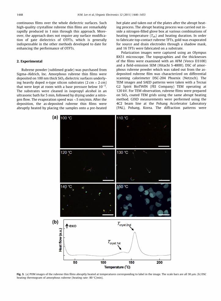
Fig. 3. (a) POM images of the rubrene thin films abruptly heated at temperaturesheating thermogram of amorphous rubrene (heating rate: 80 �C/min).
hot plate and taken out of the plates after the abrupt heat-ing process. The abrupt heating process was carried out in-side a nitrogen-filled glove box at various combinations ofheating temperature (Tah) and heating duration. In orderto fabricate top-contact rubrene TFTs, gold was evaporatedfor source and drain electrodes through a shadow mask,and 16 TFTs were fabricated on a substrate.
Polarization images were captured using an OlympusBX51 microscope. The topographies and the thicknessesof the films were examined with an AFM (Veeco D3100)and a field-emission SEM (Hitachi S-4800). DSC of amor-phous rubrene powder which was raked out from the as-deposited rubrene film was characterized on differentialscanning calorimeter DSC-204 Phoenix (Netzsch). TheTEM images and SAED patterns were taken with a TecnaiG2 Spirit BioTWIN (FEI Company) TEM operating at120 kV. For TEM observation, rubrene films were preparedon SiO2 coated TEM grids using the same abrupt heatingmethod. GIXD measurements were performed using the4C2 beam line at the Pohang Accelerator Laboratory(PAL), Pohang, Korea. The diffraction patterns were
corresponding to label in the image. The scale bars are all 30 lm. (b) DSC
H.M. Lee et al. / Organic Electronics 12 (2011) 1446–1453 1449
recorded using a MarCCD detector. The grazing-incidenceangle of the X-ray beam (k = 1.3807 Å) was varied between0.14� and 0.25�, and the sample-to-detector distance(143.5 mm) was calibrated using a silver behanate stan-dard sample and the footprint of the X-ray beam on thespecimen surface was 1 mm � 5 mm. The diffraction datawere displayed as an intensity map in which qxy is thein-plane momentum transfer and qz is the out-of-planemomentum transfer. The TFT characteristics were evalu-ated under ambient air conditions with a Keithley 4200semiconductor characterization system.
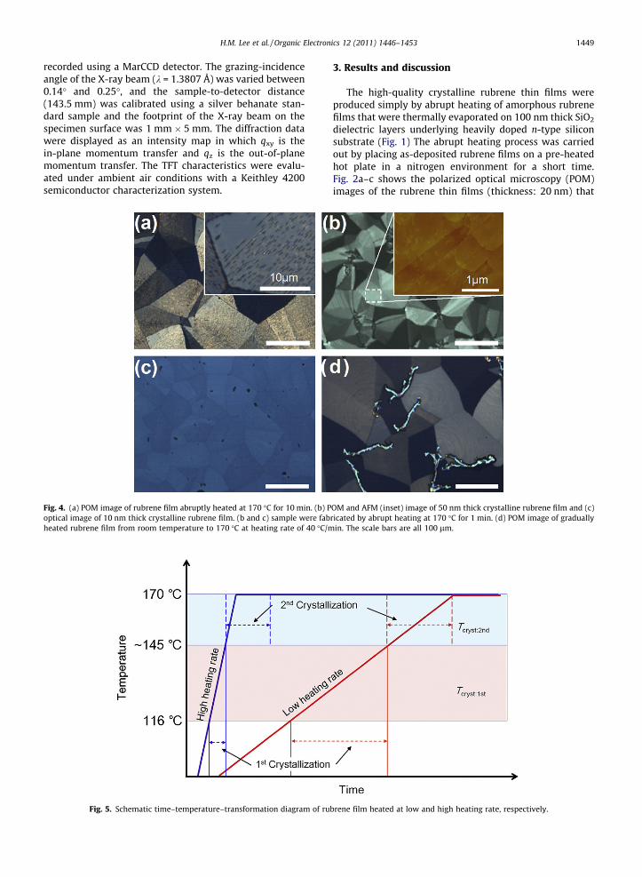
Fig. 4. (a) POM image of rubrene film abruptly heated at 170 �C for 10 min. (b) Poptical image of 10 nm thick crystalline rubrene film. (b and c) sample were fabheated rubrene film from room temperature to 170 �C at heating rate of 40 �C/m
Fig. 5. Schematic time–temperature–transformation diagram of ru
3. Results and discussion
The high-quality crystalline rubrene thin films wereproduced simply by abrupt heating of amorphous rubrenefilms that were thermally evaporated on 100 nm thick SiO2
dielectric layers underlying heavily doped n-type siliconsubstrate (Fig. 1) The abrupt heating process was carriedout by placing as-deposited rubrene films on a pre-heatedhot plate in a nitrogen environment for a short time.Fig. 2a–c shows the polarized optical microscopy (POM)images of the rubrene thin films (thickness: 20 nm) that
OM and AFM (inset) image of 50 nm thick crystalline rubrene film and (c)ricated by abrupt heating at 170 �C for 1 min. (d) POM image of gradually
in. The scale bars are all 100 lm.
brene film heated at low and high heating rate, respectively.
1450 H.M. Lee et al. / Organic Electronics 12 (2011) 1446–1453
were abruptly heated at different temperatures. The as-deposited rubrene film did not display a crystalline featureunder polarized light (Supporting Information, Fig. S1a).However, the rubrene films that underwent the abruptheating process exhibited strong birefringence in thePOM images, indicating that crystalline structures wereformed [22]. Upon abrupt heating at a relatively low tem-perature of 125 �C for 5 min, branch-like crystalline struc-tures appeared (Fig. 2a). Scanning electron microscopy(SEM) images show that the branch-like crystallites withwidths of a few 100 nm and lengths of several lm areembedded in an amorphous rubrene matrix (inset ofFig. 2a). Interestingly, when Tah was increased to 150 �C,disk-shaped platelet crystallites with diameters of severaltens lm were formed in addition to the branch-like crys-tallites (Fig. 2b). With a further increase of Tah to 170 �C,novel crystalline rubrene films, that is, continuous crystal-line films consisting of large-sized and well-faceted do-mains were created over the whole SiO2 surfaces(Fig. 2c). No colour variation was observed within a singledomain under POM investigation, suggesting that a do-main is composed of a single crystalline grain. Theaverage grain size was ca. 80 lm and the grains were inter-connected with one another, as shown in the POM image of
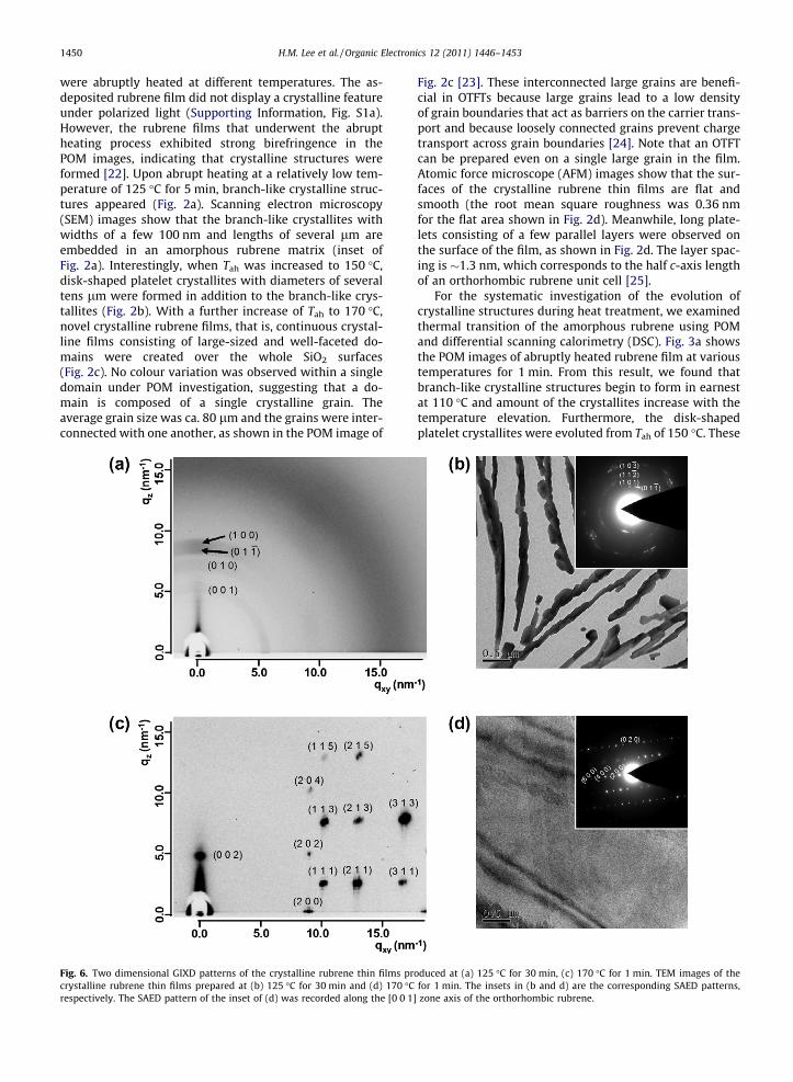
Fig. 6. Two dimensional GIXD patterns of the crystalline rubrene thin films prcrystalline rubrene thin films prepared at (b) 125 �C for 30 min and (d) 170 �Crespectively. The SAED pattern of the inset of (d) was recorded along the [0 0 1
Fig. 2c [23]. These interconnected large grains are benefi-cial in OTFTs because large grains lead to a low densityof grain boundaries that act as barriers on the carrier trans-port and because loosely connected grains prevent chargetransport across grain boundaries [24]. Note that an OTFTcan be prepared even on a single large grain in the film.Atomic force microscope (AFM) images show that the sur-faces of the crystalline rubrene thin films are flat andsmooth (the root mean square roughness was 0.36 nmfor the flat area shown in Fig. 2d). Meanwhile, long plate-lets consisting of a few parallel layers were observed onthe surface of the film, as shown in Fig. 2d. The layer spac-ing is �1.3 nm, which corresponds to the half c-axis lengthof an orthorhombic rubrene unit cell [25].
For the systematic investigation of the evolution ofcrystalline structures during heat treatment, we examinedthermal transition of the amorphous rubrene using POMand differential scanning calorimetry (DSC). Fig. 3a showsthe POM images of abruptly heated rubrene film at varioustemperatures for 1 min. From this result, we found thatbranch-like crystalline structures begin to form in earnestat 110 �C and amount of the crystallites increase with thetemperature elevation. Furthermore, the disk-shapedplatelet crystallites were evoluted from Tah of 150 �C. These
oduced at (a) 125 �C for 30 min, (c) 170 �C for 1 min. TEM images of thefor 1 min. The insets in (b and d) are the corresponding SAED patterns,
] zone axis of the orthorhombic rubrene.
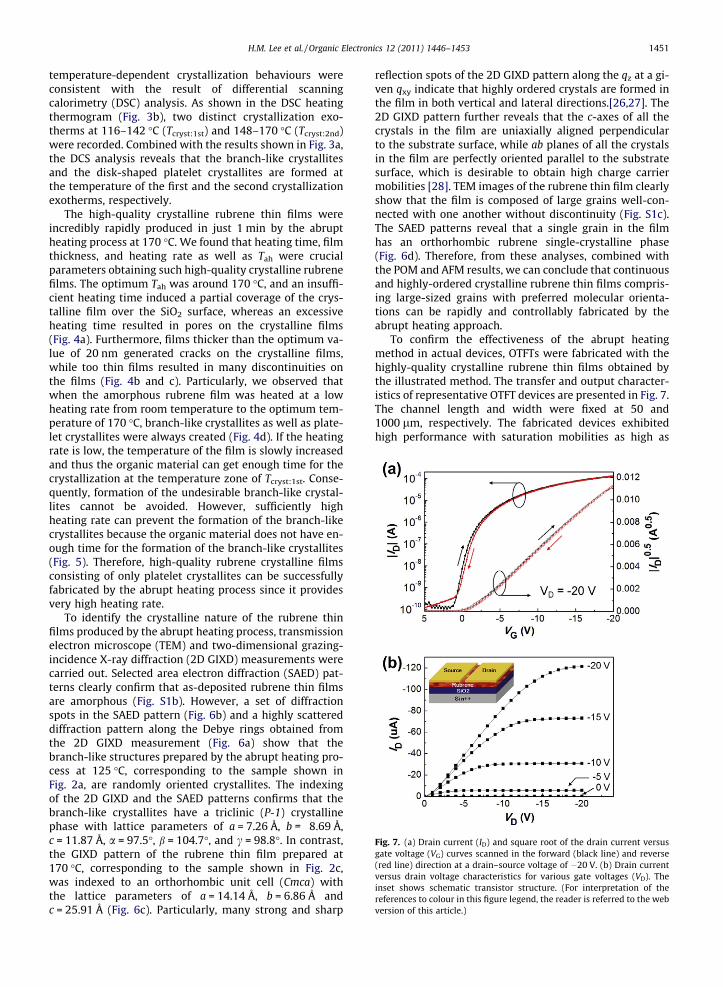
Fig. 7. (a) Drain current (ID) and square root of the drain current versusgate voltage (VG) curves scanned in the forward (black line) and reverse(red line) direction at a drain–source voltage of �20 V. (b) Drain currentversus drain voltage characteristics for various gate voltages (VD). Theinset shows schematic transistor structure. (For interpretation of thereferences to colour in this figure legend, the reader is referred to the webversion of this article.)
H.M. Lee et al. / Organic Electronics 12 (2011) 1446–1453 1451
temperature-dependent crystallization behaviours wereconsistent with the result of differential scanningcalorimetry (DSC) analysis. As shown in the DSC heatingthermogram (Fig. 3b), two distinct crystallization exo-therms at 116–142 �C (Tcryst:1st) and 148–170 �C (Tcryst:2nd)were recorded. Combined with the results shown in Fig. 3a,the DCS analysis reveals that the branch-like crystallitesand the disk-shaped platelet crystallites are formed atthe temperature of the first and the second crystallizationexotherms, respectively.
The high-quality crystalline rubrene thin films wereincredibly rapidly produced in just 1 min by the abruptheating process at 170 �C. We found that heating time, filmthickness, and heating rate as well as Tah were crucialparameters obtaining such high-quality crystalline rubrenefilms. The optimum Tah was around 170 �C, and an insuffi-cient heating time induced a partial coverage of the crys-talline film over the SiO2 surface, whereas an excessiveheating time resulted in pores on the crystalline films(Fig. 4a). Furthermore, films thicker than the optimum va-lue of 20 nm generated cracks on the crystalline films,while too thin films resulted in many discontinuities onthe films (Fig. 4b and c). Particularly, we observed thatwhen the amorphous rubrene film was heated at a lowheating rate from room temperature to the optimum tem-perature of 170 �C, branch-like crystallites as well as plate-let crystallites were always created (Fig. 4d). If the heatingrate is low, the temperature of the film is slowly increasedand thus the organic material can get enough time for thecrystallization at the temperature zone of Tcryst:1st. Conse-quently, formation of the undesirable branch-like crystal-lites cannot be avoided. However, sufficiently highheating rate can prevent the formation of the branch-likecrystallites because the organic material does not have en-ough time for the formation of the branch-like crystallites(Fig. 5). Therefore, high-quality rubrene crystalline filmsconsisting of only platelet crystallites can be successfullyfabricated by the abrupt heating process since it providesvery high heating rate.
To identify the crystalline nature of the rubrene thinfilms produced by the abrupt heating process, transmissionelectron microscope (TEM) and two-dimensional grazing-incidence X-ray diffraction (2D GIXD) measurements werecarried out. Selected area electron diffraction (SAED) pat-terns clearly confirm that as-deposited rubrene thin filmsare amorphous (Fig. S1b). However, a set of diffractionspots in the SAED pattern (Fig. 6b) and a highly scattereddiffraction pattern along the Debye rings obtained fromthe 2D GIXD measurement (Fig. 6a) show that thebranch-like structures prepared by the abrupt heating pro-cess at 125 �C, corresponding to the sample shown inFig. 2a, are randomly oriented crystallites. The indexingof the 2D GIXD and the SAED patterns confirms that thebranch-like crystallites have a triclinic (P-1) crystallinephase with lattice parameters of a = 7.26 Å, b = 8.69 Å,c = 11.87 Å, a = 97.5�, b = 104.7�, and c = 98.8�. In contrast,the GIXD pattern of the rubrene thin film prepared at170 �C, corresponding to the sample shown in Fig. 2c,was indexed to an orthorhombic unit cell (Cmca) withthe lattice parameters of a = 14.14 Å, b = 6.86 Å andc = 25.91 Å (Fig. 6c). Particularly, many strong and sharp
reflection spots of the 2D GIXD pattern along the qz at a gi-ven qxy indicate that highly ordered crystals are formed inthe film in both vertical and lateral directions.[26,27]. The2D GIXD pattern further reveals that the c-axes of all thecrystals in the film are uniaxially aligned perpendicularto the substrate surface, while ab planes of all the crystalsin the film are perfectly oriented parallel to the substratesurface, which is desirable to obtain high charge carriermobilities [28]. TEM images of the rubrene thin film clearlyshow that the film is composed of large grains well-con-nected with one another without discontinuity (Fig. S1c).The SAED patterns reveal that a single grain in the filmhas an orthorhombic rubrene single-crystalline phase(Fig. 6d). Therefore, from these analyses, combined withthe POM and AFM results, we can conclude that continuousand highly-ordered crystalline rubrene thin films compris-ing large-sized grains with preferred molecular orienta-tions can be rapidly and controllably fabricated by theabrupt heating approach.
To confirm the effectiveness of the abrupt heatingmethod in actual devices, OTFTs were fabricated with thehighly-quality crystalline rubrene thin films obtained bythe illustrated method. The transfer and output character-istics of representative OTFT devices are presented in Fig. 7.The channel length and width were fixed at 50 and1000 lm, respectively. The fabricated devices exhibitedhigh performance with saturation mobilities as high as
1452 H.M. Lee et al. / Organic Electronics 12 (2011) 1446–1453
1.21 cm2 V�1 s�1 and on/off current ratios higher than 106
under ambient conditions. Threshold voltages deduced bythe linear extrapolation of the saturation region in thesquare root of the drain current versus gate voltage wereas small as �1.0 V. In addition, as shown in Fig. 5a, the de-vices showed little hysteresis between forward and reversescans, and their subthreshold swings were as low as0.62 V/decade. Both low hysteresis and small subthresholdswing indicate that the prepared high-quality crystallinerubrene films have a low density of traps [29]. It is note-worthy that the overall characteristics of our TFT devicesare quite comparable to those of the state-of-the-art OTFTs[30,31]. From the random testing of 10 devices, a good uni-formity in device performance was also observed: theaverage motility was 1.03 cm2 V�1 s�1 with a standarddeviation of 0.11 cm2 V�1 s�1, and the average thresholdvoltage was �0.65 V with a standard deviation of 0.18 V.
4. Conclusions
We have presented a straightforward approach to fabri-cate high-quality crystalline rubrene active layers forOTFTs. Simply by an abrupt heating process, crystallinerubrene semiconductor thin films comprising large, highlyordered, and interconnected single-crystalline grains withdesirable molecular orientation can be controllably fabri-cated. High-performance OTFTs with characteristics betterthan a-Si:H TFT devices were reproducibly produced usingthe rubrene thin films. Such high-quality crystallinerubrene thin films are remarkably rapidly produced with-out any surface modification of gate dielectrics, therebydemonstrating that the approach is a very simple yet effec-tive route to produce high-performance OTFTs. Moreover,the approach is also compatible with polymeric substratesdue to the short processing time at a relatively low tem-perature of 170 �C, as shown in our preliminary results(Fig. S2). We believe that our approach is very promisingfor practical applications of rubrene semiconductors to or-ganic electronics.
Acknowledgement
This work was supported by the National ResearchFoundation of Korea (NRF) Grant funded by the Korea gov-ernment (MEST) (No. 2010-0026150).
Appendix A. Supplementary data
Supplementary data associated with this article can befound, in the online version, at doi:10.1016/j.orgel.2011.05.015.
References
[1] G. Gelinck, P. Heremans, K. Nomoto, T.D. Anthopoulos, Organictransistors in optical displays and microelectronic applications, Adv.Mater. 22 (2010) 3778–3798.
[2] T. Sekitani, H. Nakajima, H. Maeda, T. Fukushima, T. Aida, K. Hata, T.Someya, Stretchable active-matrix organic light-emitting diodedisplay using printable elastic conductors, Nat. Mater. 8 (2009)494–499.
[3] E.C.P. Smits, S.G.J. Mathijssen, P.A. van Hal, S. Setayesh, T.C.T. Geuns,K. Mutsaers, E. Cantatore, H.J. Wondergem, O. Werzer, R. Resel, M.Kemerink, S. Kirchmeyer, A.M. Muzafarov, S.A. Ponomarenko, B. deBoer, P.W.M. Blom, D.M. de Leeuw, Bottom-up organic integratedcircuits, Nature 455 (2008) 956–959.
[4] B. Crone, A. Dodabalapur, Y.Y. Lin, R.W. Filas, Z. Bao, A. LaDuca, R.Sarpeshkar, H.E. Katz, W. Li, Large-scale complementary integratedcircuits based on organic transistors, Nature 403 (2000) 521–523.
[5] R. Rotzoll, S. Mohapatra, V. Olariu, R. Wenz, M. Grigas, K. Dimmler, O.Shchekin, A. Dodabalapur, Radio frequency rectifiers based onorganic thin-film transistors, Appl. Phys. Lett. 88 (2006) 123502.
[6] D.J. Gundlach, Low power high impact, Nat. Mater. 6 (2007) 173–174.[7] M.T. Martinez, Y.C. Tseng, N. Ormategui, I. Loinaz, R. Eritja, J. Bokor,
Label-free DNA biosensors based on functionalized carbon nanotubefield effect transistors, Nano Lett. 9 (2009) 530–536.
[8] T. Someya, T. Sekitani, S. Iba, Y. Kato, H. Kawaguchi, T. Sakurai, Alarge-area flexible pressure sensor matrix with organic field-effecttransistors for artificial skin applications, Proc. Natl. Acad. Sci. USA101 (2004) 9966–9970.
[9] G. Horowitz, Organic field-effect transistors, Adv. Mater. 10 (1998)365–377.
[10] J. Rivnay, L.H. Jimison, J.E. Northrup, M.F. Toney, R. Noriega, S.F. Lu,T.J. Marks, A. Facchetti, A. Salleo, Large modulation of carriertransport by grain-boundary molecular packing and microstructurein organic thin films, Nat. Mater. 8 (2009) 952–958.
[11] V.C. Sundar, J. Zaumseil, V. Podzorov, E. Menard, R.L. Willett, T.Someya, M.E. Gershenson, J.A. Rogers, Elastomeric transistor stamps:reversible probing of charge transport in organic crystals, Science303 (2004) 1644–1646.
[12] J. Takeya, M. Yamagishi, Y. Tominari, R. Hirahara, Y. Nakazawa, T.Nishikawa, T. Kawase, T. Shimoda, S. Ogawa, Very high-mobilityorganic single-crystal transistors with in-crystal conductionchannels, Appl. Phys. Lett. 90 (2007) 102120.
[13] D. Braga, G. Horowitz, High-performance organic field-effecttransistors, Adv. Mater. 21 (2009) 1473–1486.
[14] A.L. Briseno, S.C.B. Mannsfeld, M.M. Ling, S.H. Liu, R.J. Tseng, C. Reese,M.E. Roberts, Y. Yang, F. Wudl, Z.N. Bao, Patterning organic single-crystal transistor arrays, Nature 444 (2006) 913–917.
[15] L. Luo, G. Liu, L.W. Huang, X.Q. Cao, M. Liu, H.B. Fu, J.N. Yao, Solution-based patterned growth of rubrene nanocrystals for organic fieldeffect transistors, Appl. Phys. Lett. 95 (2009) 263312.
[16] B. Park, I. In, P. Gopalan, P.G. Evans, S. King, P.F. Lyman, Enhancedhole mobility in ambipolar rubrene thin film transistors onpolystyrene, Appl. Phys. Lett. 92 (2008) 133302.
[17] S.W. Park, J.M. Hwang, J.M. Choi, D.K. Hwang, M.S. Oh, J.H. Kim, S.Ima, Rubrene thin-film transistors with crystalline and amorphouschannels, Appl. Phys. Lett. 90 (2007) 153512.
[18] Y. Chen, I. Shih, High mobility organic thin film transistors based onmonocrystalline rubrene films grown by low pressure hot walldeposition, Appl. Phys. Lett. 94 (2009) 083304.
[19] C.H. Hsu, J. Deng, C.R. Staddon, P.H. Beton, Growth front nucleationof rubrene thin films for high mobility organic transistors, Appl.Phys. Lett. 91 (2007) 193505.
[20] Z.F. Li, J. Du, Q. Tang, F. Wang, J.B. Xu, J.C. Yu, Q.A. Miao, Inducedcrystallization of rubrene in thin-film transistors, Adv. Mater. 22(2010) 3242–3246.
[21] N. Stingelin-Stutzmann, E. Smits, H. Wondergem, C. Tanase, P. Blom,P. Smith, D. De Leeuw, Organic thin-film electronics from vitreoussolution-processed rubrene hypereutectics, Nat. Mater. 4 (2005)601–606.
[22] Y. Luo, F. Gustavo, J.Y. Henry, F. Mathevet, F. Lefloch, M. Sanquer, P.Rannou, B. Grevin, Probing local electronic transport at the organicsingle-crystal/dielectric interface, Adv. Mater. 19 (2007) 2267–2273.
[23] X.N. Sun, C.A. Di, Y.Q. Liu, Engineering of the dielectric-semiconductor interface in organic field-effect transistors, J. Mater.Chem. 20 (2010) 2599–2611.
[24] R. Schmechel, H. von Seggern, Electronic traps in organic transportlayers, Phys. Stat. Sol. (a) 201 (2004) 1215–1235.
[25] E. Menard, A. Marchenko, V. Podzorov, M.E. Gershenson, D. Fichou,J.A. Rogers, Nanoscale surface morphology and rectifying behavior ofa bulk single-crystal organic semiconductor, Adv. Mater. 18 (2006)1552–1556.
[26] J.A. Lim, W.H. Lee, H.S. Lee, J.H. Lee, Y.D. Park, K. Cho, Self-organization of ink-jet-printed triisopropylsilylethynyl pentacenevia evaporation-induced flows in a drying droplet, Adv. Funct. Mater.18 (2008) 229–234.
[27] H.C. Yang, T.J. Shin, M.M. Ling, K. Cho, C.Y. Ryu, Z.N. Bao, ConductingAFM and 2D GIXD studies on pentacene thin films, J. Am. Chem. Soc.127 (2005) 11542–11543.
H.M. Lee et al. / Organic Electronics 12 (2011) 1446–1453 1453
[28] G.J. Nan, X.D. Yang, L.J. Wang, Z.G. Shuai, Y. Zhao, Nuclear tunnelingeffects of charge transport in rubrene, tetracene, and pentacene,Phys. Rev. B 79 (2009).
[29] W.L. Kalb, T. Mathis, S. Haas, A.F. Stassen, B. Batlogg, Organic smallmolecule field-effect transistors with Cytop (TM) gate dielectric:eliminating gate bias stress effects, Appl. Phys. Lett. 90 (2007)092104.
[30] H. Klauk, Organic thin-film transistors, Chem. Soc. Rev. 39 (2010)2643–2666.
[31] W.P. Wu, Y.Q. Liu, D.B. Zhu, pi-Conjugated molecules with fusedrings for organic field-effect transistors: design, synthesis andapplications, Chem. Soc. Rev. 39 (2010) 1489–1502.
Related Documents