Wright State University Wright State University CORE Scholar CORE Scholar Browse all Theses and Dissertations Theses and Dissertations 2006 A Study of the Impact of Hardware Design Choices on the System A Study of the Impact of Hardware Design Choices on the System Impulse Response of a Signal-Level Radar Simulation Impulse Response of a Signal-Level Radar Simulation Kelly Renee Feirstine Wright State University Follow this and additional works at: https://corescholar.libraries.wright.edu/etd_all Part of the Electrical and Computer Engineering Commons Repository Citation Repository Citation Feirstine, Kelly Renee, "A Study of the Impact of Hardware Design Choices on the System Impulse Response of a Signal-Level Radar Simulation" (2006). Browse all Theses and Dissertations. 42. https://corescholar.libraries.wright.edu/etd_all/42 This Thesis is brought to you for free and open access by the Theses and Dissertations at CORE Scholar. It has been accepted for inclusion in Browse all Theses and Dissertations by an authorized administrator of CORE Scholar. For more information, please contact [email protected].

Welcome message from author
This document is posted to help you gain knowledge. Please leave a comment to let me know what you think about it! Share it to your friends and learn new things together.
Transcript
Wright State University Wright State University
CORE Scholar CORE Scholar
Browse all Theses and Dissertations Theses and Dissertations
2006
A Study of the Impact of Hardware Design Choices on the System A Study of the Impact of Hardware Design Choices on the System
Impulse Response of a Signal-Level Radar Simulation Impulse Response of a Signal-Level Radar Simulation
Kelly Renee Feirstine Wright State University
Follow this and additional works at: https://corescholar.libraries.wright.edu/etd_all
Part of the Electrical and Computer Engineering Commons
Repository Citation Repository Citation Feirstine, Kelly Renee, "A Study of the Impact of Hardware Design Choices on the System Impulse Response of a Signal-Level Radar Simulation" (2006). Browse all Theses and Dissertations. 42. https://corescholar.libraries.wright.edu/etd_all/42
This Thesis is brought to you for free and open access by the Theses and Dissertations at CORE Scholar. It has been accepted for inclusion in Browse all Theses and Dissertations by an authorized administrator of CORE Scholar. For more information, please contact [email protected].

A Study of the Impact of Hardware Design Choiceson the System Impulse Response of a Signal-level
Radar Simulation
A thesis submitted in partial fulfillmentof the requirements for the degree of
Master of Science in Engineering
by
Kelly R. FeirstineDepartment of Electrical Engineering
Wright State University
2006Wright State University

Wright State UniversitySCHOOL OF GRADUATE STUDIES
August 30, 2006
I HEREBY RECOMMEND THAT THE THESIS PREPARED UNDER MY SUPER-VISION BY Kelly R. Feirstine ENTITLED A Study of the Impact of Hardware DesignChoices on the System Impulse Response of a Signal-level Radar Simulation BE AC-CEPTED IN PARTIAL FULFILLMENT OF THE REQUIREMENTS FOR THE DE-GREE OF Master of Science in Engineering .
Brian Rigling, Ph.D.Thesis Director
Fred Garber, Ph.D.Department Chair
Committee onFinal Examination
Brian Rigling , Ph.D.
Fred Garber , Ph.D.
Marty Emmert , Ph.D.
Joseph F. Thomas, Jr., Ph.D.Dean, School of Graduate Studies
ABSTRACT
Feirstine, Kelly. M.S., Department of Electrical Engineering, Wright State University, 2006 . AStudy of the Impact of Hardware Design Choices on the System Impulse Response of a Signal-levelRadar Simulation.
The main goal of this research is to study the effect of hardware design choices at the signal-
level of an end-to-end radar system. An implementation of waveform diversity concepts, or the use
of various waveforms in both transmit and receive is employed. An end-to-end Matlab simulation
is developed such that the system impulse response to hardware imperfections and waveform pa-
rameters such as bandwidth and frequency channel spacing can be analyzed. Multiple frequency
channels as well as multiple pulses are also considered in the research.
All hardware components are nonlinear to some degree. The nonlinearities of the hardware give
rise to unwanted spectral components in the output. Therefore, models that simulate the behavior of
both ideal and non-ideal hardware components are developed. A user friendly interface is developed
in which each hardware component can be interchanged between the ideal and non-ideal model. In
studying both the system impulse response to ideal components as well as the response to non-
ideal components, the impact of the nonlinearities on cross-correlation signal detection and range-
Doppler can be analyzed.
iii

Contents
1 Introduction 11.1 Background Information . . . . . . . . . . . . . . . . . . . . . . . . . . . . . . . 11.2 Technical Approach . . . . . . . . . . . . . . . . . . . . . . . . . . . . . . . . . . 2
1.2.1 Simulation Environment . . . . . . . . . . . . . . . . . . . . . . . . . . . 21.2.2 Mathematical Background . . . . . . . . . . . . . . . . . . . . . . . . . . 4
1.3 Matlab Simulation . . . . . . . . . . . . . . . . . . . . . . . . . . . . . . . . . . 81.3.1 Transmit Signal Flow . . . . . . . . . . . . . . . . . . . . . . . . . . . . . 81.3.2 Receive Signal Flow . . . . . . . . . . . . . . . . . . . . . . . . . . . . . 91.3.3 Detection Process . . . . . . . . . . . . . . . . . . . . . . . . . . . . . . . 101.3.4 Matlab GUI . . . . . . . . . . . . . . . . . . . . . . . . . . . . . . . . . . 11
2 Ideal Simulation 142.1 Component Modules . . . . . . . . . . . . . . . . . . . . . . . . . . . . . . . . . 14
2.1.1 Waveform Generator . . . . . . . . . . . . . . . . . . . . . . . . . . . . . 142.1.2 Frequency Modulation . . . . . . . . . . . . . . . . . . . . . . . . . . . . 152.1.3 Amplifier . . . . . . . . . . . . . . . . . . . . . . . . . . . . . . . . . . . 162.1.4 Converters . . . . . . . . . . . . . . . . . . . . . . . . . . . . . . . . . . 162.1.5 Time Delay Network . . . . . . . . . . . . . . . . . . . . . . . . . . . . . 17
2.2 Software Testing . . . . . . . . . . . . . . . . . . . . . . . . . . . . . . . . . . . 172.2.1 Simulation . . . . . . . . . . . . . . . . . . . . . . . . . . . . . . . . . . 172.2.2 Results . . . . . . . . . . . . . . . . . . . . . . . . . . . . . . . . . . . . 51
3 Non-ideal Simulation 593.1 Component Modules . . . . . . . . . . . . . . . . . . . . . . . . . . . . . . . . . 59
3.1.1 Frequency Modulation . . . . . . . . . . . . . . . . . . . . . . . . . . . . 623.1.2 Amplifier . . . . . . . . . . . . . . . . . . . . . . . . . . . . . . . . . . . 633.1.3 Converters . . . . . . . . . . . . . . . . . . . . . . . . . . . . . . . . . . 643.1.4 Analog Filter . . . . . . . . . . . . . . . . . . . . . . . . . . . . . . . . . 673.1.5 Time Delay Network . . . . . . . . . . . . . . . . . . . . . . . . . . . . . 67
3.2 Software Testing . . . . . . . . . . . . . . . . . . . . . . . . . . . . . . . . . . . 683.2.1 Simulation . . . . . . . . . . . . . . . . . . . . . . . . . . . . . . . . . . 683.2.2 Results . . . . . . . . . . . . . . . . . . . . . . . . . . . . . . . . . . . . 84
iv
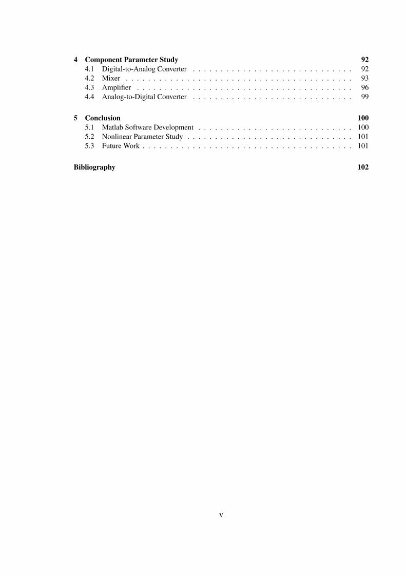
4 Component Parameter Study 924.1 Digital-to-Analog Converter . . . . . . . . . . . . . . . . . . . . . . . . . . . . . 924.2 Mixer . . . . . . . . . . . . . . . . . . . . . . . . . . . . . . . . . . . . . . . . . 934.3 Amplifier . . . . . . . . . . . . . . . . . . . . . . . . . . . . . . . . . . . . . . . 964.4 Analog-to-Digital Converter . . . . . . . . . . . . . . . . . . . . . . . . . . . . . 99
5 Conclusion 1005.1 Matlab Software Development . . . . . . . . . . . . . . . . . . . . . . . . . . . . 1005.2 Nonlinear Parameter Study . . . . . . . . . . . . . . . . . . . . . . . . . . . . . . 1015.3 Future Work . . . . . . . . . . . . . . . . . . . . . . . . . . . . . . . . . . . . . . 101
Bibliography 102
v

List of Figures
1.1 Transmit Architecture . . . . . . . . . . . . . . . . . . . . . . . . . . . . . . . . . 31.2 Receive Architecture . . . . . . . . . . . . . . . . . . . . . . . . . . . . . . . . . 31.3 Mathematical Architecture . . . . . . . . . . . . . . . . . . . . . . . . . . . . . . 41.4 Matlab Graphical User Interface . . . . . . . . . . . . . . . . . . . . . . . . . . . 121.5 GUI: Load Default Values Window . . . . . . . . . . . . . . . . . . . . . . . . . . 13
2.1 Ideal Simulation: Transmitted Waveforms: I-channel . . . . . . . . . . . . . . . . 192.2 Ideal Simulation: Transmitted Waveforms: Q-channel . . . . . . . . . . . . . . . . 202.3 Ideal Simulation: Summation of digital signals from all three branches . . . . . . . 212.4 Ideal Simulation: Frequency spectrum of summed signal . . . . . . . . . . . . . . 222.5 Ideal Simulation: DAC output signal . . . . . . . . . . . . . . . . . . . . . . . . . 232.6 Ideal Simulation: DAC output frequency spectrum . . . . . . . . . . . . . . . . . 242.7 Ideal Simulation: RF mixer output signal . . . . . . . . . . . . . . . . . . . . . . 252.8 Ideal Simulation: RF mixer output frequency spectrum . . . . . . . . . . . . . . . 262.9 Ideal Simulation: High pass filter spectrum of filter following RF mixer . . . . . . 272.10 Ideal Simulation: High pass filter output signal spectrum following RF mixer . . . 282.11 Ideal Simulation: Time Delayed Signal . . . . . . . . . . . . . . . . . . . . . . . . 302.12 Ideal Simulation: RF demodulation output signal . . . . . . . . . . . . . . . . . . 312.13 Ideal Simulation: RF demodulation output frequency spectrum . . . . . . . . . . . 322.14 Ideal Simulation: Low pass filter spectrum of filter following RF demodulation on
receive . . . . . . . . . . . . . . . . . . . . . . . . . . . . . . . . . . . . . . . . . 332.15 Ideal Simulation: Low pass filter output frequency spectrum following RF demod-
ulation on receive . . . . . . . . . . . . . . . . . . . . . . . . . . . . . . . . . . . 342.16 Ideal Simulation: ADC output signal . . . . . . . . . . . . . . . . . . . . . . . . . 352.17 Ideal Simulation: ADC output frequency spectrum . . . . . . . . . . . . . . . . . 362.18 Ideal Simulation: IF demodulated I-channel signal: Branch 1 . . . . . . . . . . . . 372.19 Ideal Simulation: IF demodulated I-channel frequency spectrum: Branch 1 . . . . . 382.20 Ideal Simulation: IF demodulated Q-channel signal: Branch 1 . . . . . . . . . . . 392.21 Ideal Simulation: IF demodulated Q-channel frequency spectrum: Branch 1 . . . . 402.22 Ideal Simulation: IF demodulated I-channel signal: Branch 2 . . . . . . . . . . . . 412.23 Ideal Simulation: IF demodulated I-channel frequency spectrum: Branch 2 . . . . . 422.24 Ideal Simulation: IF demodulated Q-channel signal: Branch 2 . . . . . . . . . . . 432.25 Ideal Simulation: IF demodulated Q-channel frequency spectrum: Branch 2 . . . . 442.26 Ideal Simulation: IF demodulated I-channel signal: Branch 3 . . . . . . . . . . . . 452.27 Ideal Simulation: IF demodulated I-channel frequency spectrum: Branch 3 . . . . . 462.28 Ideal Simulation: IF demodulated Q-channel signal: Branch 3 . . . . . . . . . . . 472.29 Ideal Simulation: IF demodulated Q-channel frequency spectrum: Branch 3 . . . . 48
vi

2.30 Ideal Simulation: Baseband low pass filter frequency spectrum used for all branchesand channels . . . . . . . . . . . . . . . . . . . . . . . . . . . . . . . . . . . . . . 49
2.31 Ideal Simulation: Received signal spectrum after low pass filter to remove harmonics 502.32 Ideal Simulation: Cross-correlation . . . . . . . . . . . . . . . . . . . . . . . . . . 522.33 Ideal Simulation: Range-Doppler plots for zero Doppler shift . . . . . . . . . . . . 532.34 Ideal Simulation: Range-Doppler plots for positive Doppler shift . . . . . . . . . . 552.35 Ideal Simulation: Range-Doppler plots for negative Doppler shift . . . . . . . . . . 56
3.1 Two-tone Intermodulation Distortion . . . . . . . . . . . . . . . . . . . . . . . . . 603.2 Third Order Nonlinear Intercept Point . . . . . . . . . . . . . . . . . . . . . . . . 613.3 Nonlinear Compression Point . . . . . . . . . . . . . . . . . . . . . . . . . . . . . 613.4 Non-ideal Simulation: Nonlinear DAC output signal . . . . . . . . . . . . . . . . 703.5 Non-ideal Simulation: Nonlinear DAC output signal spectrum . . . . . . . . . . . 713.6 Non-ideal Simulation: Low pass filtered signal after filtering out unwanted DAC
harmonics . . . . . . . . . . . . . . . . . . . . . . . . . . . . . . . . . . . . . . . 723.7 Non-ideal Simulation: Low pass filtered signal frequency spectrum after filtering
out unwanted DAC harmonics . . . . . . . . . . . . . . . . . . . . . . . . . . . . 733.8 Non-ideal Simulation: RF mixer output signal . . . . . . . . . . . . . . . . . . . . 743.9 Non-ideal Simulation: RF mixer output signal frequency spectrum . . . . . . . . . 753.10 Non-ideal Simulation: High pass filter output signal following RF mixer . . . . . . 763.11 Non-ideal Simulation: High pass filter output signal frequency spectrum following
RF mixer . . . . . . . . . . . . . . . . . . . . . . . . . . . . . . . . . . . . . . . 773.12 Non-ideal Simulation: RF demodulated signal . . . . . . . . . . . . . . . . . . . . 783.13 Non-ideal Simulation: RF demodulated signal frequency spectrum . . . . . . . . . 793.14 Non-ideal Simulation: Low pass filter output signal following RF demodulation . . 803.15 Non-ideal Simulation: Low pass filter output signal frequency spectrum following
RF demodulation . . . . . . . . . . . . . . . . . . . . . . . . . . . . . . . . . . . 813.16 Non-ideal Simulation: Nonlinear ADC output signal . . . . . . . . . . . . . . . . 823.17 Non-ideal Simulation: Nonlinear ADC output signal frequency spectrum . . . . . . 833.18 Non-ideal Simulation: Cross-correlation . . . . . . . . . . . . . . . . . . . . . . . 853.19 Non-ideal Simulation: Range-Doppler plots for zero Doppler shift . . . . . . . . . 863.20 Non-ideal Simulation: Range-Doppler plots for positive Doppler shift . . . . . . . 883.21 Non-ideal Simulation: Range-Doppler plots for negative Doppler shift . . . . . . . 89
4.1 DAC: Changes in range PSLR and ISLR due to changing the noise spectral density 934.2 DAC: Changes in Doppler PSLR and ISLR due to changing the noise spectral density 944.3 Cross-correlation plots with the DAC noise spectral density = -80 dB . . . . . . . . 954.4 Mixer: Changes in range PSLR and ISLR due to changing the conversion loss . . 954.5 Mixer: Changes in Doppler PSLR and ISLR due to changing the conversion loss . 964.6 Cross-correlation plots with the mixer conversion loss = 30 dB . . . . . . . . . . . 974.7 Cross-correlation plots with the mixer conversion loss = 40 dB . . . . . . . . . . . 98
vii
List of Tables
2.1 Ideal Waveform Generator . . . . . . . . . . . . . . . . . . . . . . . . . . . . . . 152.2 Ideal Frequency Modulation . . . . . . . . . . . . . . . . . . . . . . . . . . . . . 162.3 Ideal Time Delay Network . . . . . . . . . . . . . . . . . . . . . . . . . . . . . . 182.4 Ideal Doppler calculations: Stationary Target . . . . . . . . . . . . . . . . . . . . 542.5 Ideal Doppler calculations: Positive Velocity Target . . . . . . . . . . . . . . . . . 572.6 Ideal Doppler calculations: Negative Velocity Target . . . . . . . . . . . . . . . . 58
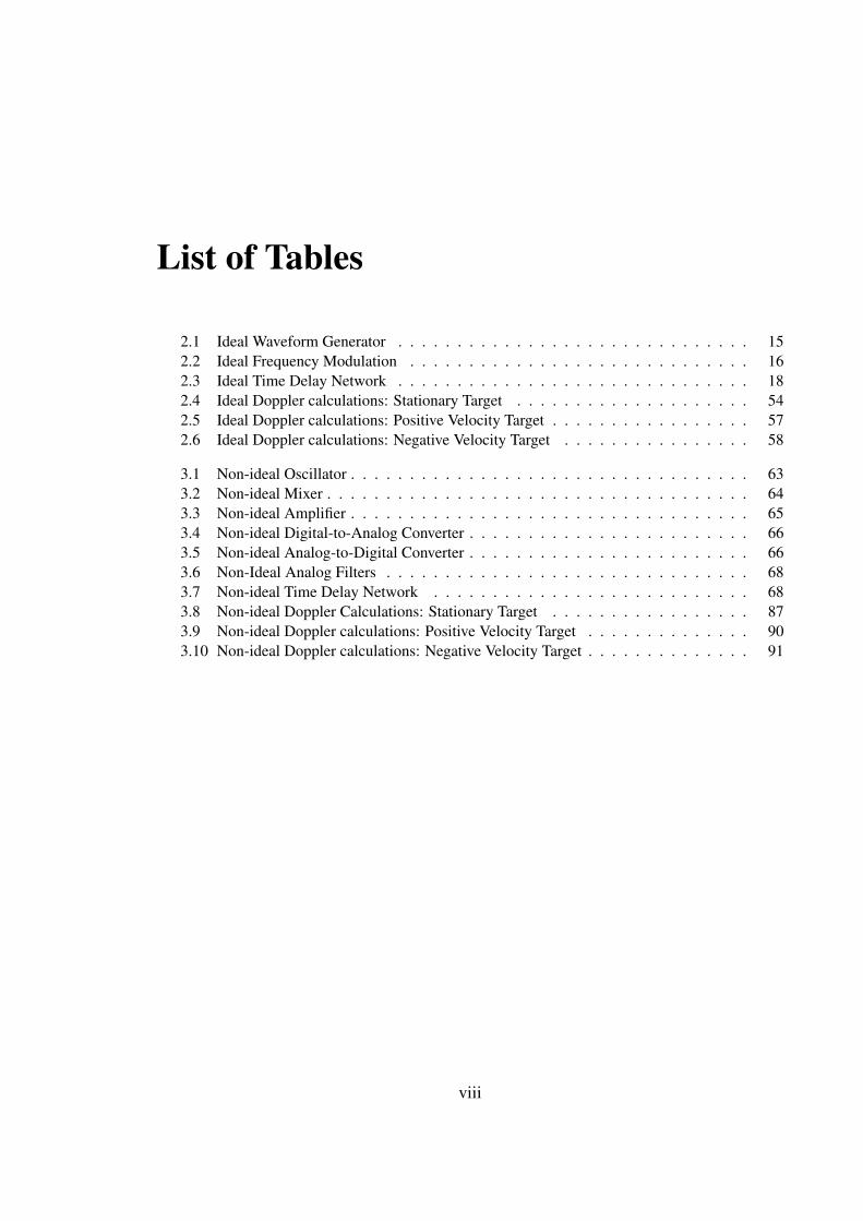
3.1 Non-ideal Oscillator . . . . . . . . . . . . . . . . . . . . . . . . . . . . . . . . . . 633.2 Non-ideal Mixer . . . . . . . . . . . . . . . . . . . . . . . . . . . . . . . . . . . . 643.3 Non-ideal Amplifier . . . . . . . . . . . . . . . . . . . . . . . . . . . . . . . . . . 653.4 Non-ideal Digital-to-Analog Converter . . . . . . . . . . . . . . . . . . . . . . . . 663.5 Non-ideal Analog-to-Digital Converter . . . . . . . . . . . . . . . . . . . . . . . . 663.6 Non-Ideal Analog Filters . . . . . . . . . . . . . . . . . . . . . . . . . . . . . . . 683.7 Non-ideal Time Delay Network . . . . . . . . . . . . . . . . . . . . . . . . . . . 683.8 Non-ideal Doppler Calculations: Stationary Target . . . . . . . . . . . . . . . . . 873.9 Non-ideal Doppler calculations: Positive Velocity Target . . . . . . . . . . . . . . 903.10 Non-ideal Doppler calculations: Negative Velocity Target . . . . . . . . . . . . . . 91
viii

Acknowledgement
I would like to extend my thanks to Dr. Brian Rigling who has not only been encouraging, but
extremely supportive throughout the completion of this project. Though I may be the only one of
his students that he would forget at times, he is still a very respectable professor with whom I have
really enjoyed working! I would also like to thank the ATK-Mission Research group, especially Mr.
Troy Klein, Dr. Robert Hawley, Dr. William Muller, and Dr. John Gwynne because without them,
this research may not have been possible.
I would like to thank Dr. Fred Garber for serving on my committee, as well as for the confidence
he had in me knowing full well how “early” I started every work day. I would also like to thank
Dr. John Emmert for serving on my committee. Your time is very much appreciated. A special
thank you goes out to those who worked in 233 with me, the usual lunch crew, and everyone else at
Wright State University that has contributed to my success as a student. Everyone was always there
to help in any way they could.
Most importantly, a special thank you goes out to my family and friends. My mother, Kathy and my
father, Rick have been nothing but supportive throughout my many years at WSU. No matter what
it is I try to accomplish, they have always been supporting of me in every way they can. Finally, I
would like to thank the many friends that I have made along the way. Without them, I would not be
the person that I am today.
ix

Chapter 1
Introduction
1.1 Background Information
The main objective of this research is to study the impact of current hardware in the implementa-
tion of waveform diversity concepts. The use of various waveforms, or signals in both transmit and
receive radar design for improving the overall system performance is referred to as waveform diver-
sity [10]. Waveform diversity can encompass many aspects of the signal design problem, including
frequency division multiplexing, pseudo-random phase coding, and pulse compression chirp rate
diversity [11]. A couple system performance characteristics addressed in this waveform diversity
study are reduction in side lobe levels of both the cross-correlation detection plots as well as in the
range-Doppler response.
An end-to-end radar system simulated at the signal-level is desired such that the effect of
hardware design choices can be analyzed. All choices of hardware components contribute in some
way to the performance of the overall system. The effect of components such as amplifiers, digital-
to-analog converters, mixers, filters, and analog-to-digital converters on a signal-level radar system
is the main focus of this research. The signal-level simulation developed and used throughout the
course of this research employs the use of binary phase-coded waveforms. The impact of the same
hardware choices using other waveforms of interest such as complementary codes, though beyond
the scope of this research, could certainly be studied in the future. The development of this signal-
level simulation will aid in the future study of other such waveform diversity concepts.
1

In determining the impact of such hardware choices, multiple frequency channels as well as
multiple pulses are considered. A requirement of the study is the capability to control the transmit
waveform on each channel for each pulse in a processing interval. The ability to change the timing
of the waveforms on each channel as well as for each pulse is also required. Also, the effect of such
waveform parameters as bandwidth and frequency channel spacing will be considered.
A user friendly interface in Matlab that gives the ability to interchange hardware components
is a secondary goal. The interface should allow the user to implement linear components as well as
those with nonlinearities. Interchanging of component types as well as nonlinear parameters should
be of ease to the user. The interface should also have the ability to determine the nonlinearity of the
components through use of cross-correlation signal detection and range-Doppler response.
1.2 Technical Approach
A signal-level Matlab simulation of an end-to-end radar system is essential such that the impact of
hardware design choices on the performance of waveform diversity techniques can be determined.
An ideal simulation is needed such that when non-ideal components with nonlinear effects are in-
terchanged with the ideal components, a performance comparison can be made. Ideal and non-ideal
models for each functional block in the system architecture are developed. The models simulate the
digital and analog performance of each step of the signal processing transmit and receive chains.
The information used to construct the models is based on typical hardware specifications.
1.2.1 Simulation Environment
The end-to-end signal-level simulation is implemented in Matlab such that the component models
are easy to manipulate and modify for future use. To make things even simpler, a separate module
for each component model is generated. The general architecture of the transmit and receive chains
chosen for the initial simulation development are shown in Figures 1.1 and 1.2. These figures do
not represent the actual hardware components, but instead the signal flow through the system. Each
of the actual hardware components can be modeled by choosing appropriate parameters based on
the component specifications.
2

Figure 1.1: Transmit Architecture
The general transmit signal flow is shown in Figure 1.1. The waveform generation block al-
lows control over the waveform selection as well as the time of the pulses. The output waveforms
from the generator block are digital. The waveforms are then digitally modulated into separate fre-
quency channels and combined. The summed signal is passed through a digital-to-analog converter.
The nonlinear DAC adds unwanted harmonics to the output signal and is therefore followed by an
analog low-pass filter to remove these harmonics. The signal is then up-converted to the RF carrier
frequency, and the output of the mixer is high-pass filtered to remove the low frequency signal. The
signal is then amplified for transmission.
Figure 1.2: Receive Architecture
The emitted signal interacts with the target in the time delay network block. The time delay
network block allows control over target parameters such as target range, range swath, and target
velocity and may in the future include array processing effects. The target returns are captured by
the receive architecture shown in Figure 1.2. The receive signal is amplified, down-converted from
the RF frequency to the intermediate frequencies, and filtered. The signal is passed through an
analog-to-digital converter. Finally, the signal is demodulated to the individual frequency channels
and passed to matched filter blocks for detection and analysis.
3
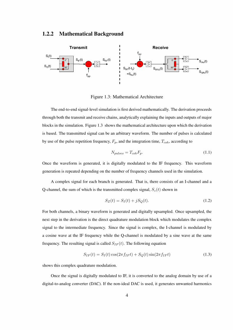
1.2.2 Mathematical Background
Figure 1.3: Mathematical Architecture
The end-to-end signal-level simulation is first derived mathematically. The derivation proceeds
through both the transmit and receive chains, analytically explaining the inputs and outputs of major
blocks in the simulation. Figure 1.3 shows the mathematical architecture upon which the derivation
is based. The transmitted signal can be an arbitrary waveform. The number of pulses is calculated
by use of the pulse repetition frequency, Fp, and the integration time, Tcoh, according to
Npulses = TcohFp. (1.1)
Once the waveform is generated, it is digitally modulated to the IF frequency. This waveform
generation is repeated depending on the number of frequency channels used in the simulation.
A complex signal for each branch is generated. That is, there consists of an I-channel and a
Q-channel, the sum of which is the transmitted complex signal, Sz(t) shown in
SZ(t) = SI(t) + jSQ(t). (1.2)
For both channels, a binary waveform is generated and digitally upsampled. Once upsampled, the
next step in the derivation is the direct quadrature modulation block which modulates the complex
signal to the intermediate frequency. Since the signal is complex, the I-channel is modulated by
a cosine wave at the IF frequency while the Q-channel is modulated by a sine wave at the same
frequency. The resulting signal is called SIF (t). The following equation
SIF (t) = SI(t) cos(2πfIF t) + SQ(t) sin(2πfIF t) (1.3)
shows this complex quadrature modulation.
Once the signal is digitally modulated to IF, it is converted to the analog domain by use of a
digital-to-analog converter (DAC). If the non-ideal DAC is used, it generates unwanted harmonics
4

in the output. In this case, a low pass filter is needed to remove the high frequency harmonic
components of the DAC output. However, if an ideal DAC is assumed, there is no need for the low
pass filter following the converter.
Now that the signal is in the analog domain, the next step in the derivation is the RF modu-
lation. The IF modulated signal, SIF (t) is modulated to the RF frequency. The resulting signal
is appropriately called SRF (t). In order that the signal is modulated to the chosen RF frequency,
a cosine modulation of SIF (t) at a frequency of (fRF − fIF ) is used. Equation 1.4 explains the
analog RF modulation mathematically.
SRF (t) = SIF (t) cos(2π(fRF − fIF )t)
= [SI(t) cos(2πfIF t) + SQ(t) sin(2πfIF t)] cos(2π(fRF − fIF )t)
= SI(t) cos(2πfIF t) cos(2π(fRF − fIF )t)
+ SQ(t) sin(2πfIF t) cos(2π(fRF − fIF )t)
= SI(t)(cos(2πfRF t) + cos(2π(2fIF − fRF )t))
+ SQ(t)(sin(2πfRF t) + sin(2π(2fIF − fRF )t))
(1.4)
Once the modulation to the RF band is complete, the signal is high pass filtered in order to keep
the part of the signal at the RF frequency and remove the low frequency components of the signal.
Equation 1.5 illustrates the removal of the components at (2fIF − fRF ) but allows the components
at fRF to pass through.
SRF (t) = HPF{SI(t)(cos(2πfRF t) + cos(2π(2fIF − fRF )t))
+ SQ(t)(sin(2πfRF t) + sin(2π(2fIF − fRF )t))}
SRF (t) = SI(t) cos(2πfRF t) + SQ(t) sin(2πfRF t)
(1.5)
Once the signal is at the RF band and the correct frequency components are removed, the
signal is propagated through the atmosphere to the target. The signal hits the target and is returned
with a time delay, t0. The calculation of the time delay is based upon target range and the speed of
light. The time delay calculation is explained in more detail in Section 2.2.1 of this document. The
target return, SRx(t) is the RF signal, SRF (t) delayed by the time delay, represented symbolically
by equation 1.6.
5
SRx(t) = SRF (t− t0)
= SI(t− t0) cos(2πfRF T ) + SQ(t− t0) sin(2πfRF (t− t0))(1.6)
On receive, the delayed signal is demodulated from the RF frequency. Since the analog modu-
lation to the RF frequency on transmit required a cosine modulation to a frequency of (fRF − fIF ),
the received signal is demodulated by the same frequency to insure that the signal SRx(t) is at the
correct IF frequency. Equation 1.7 shows this analog demodulation process mathematically. The
equation also shows that the signal contains frequency components at both high and low frequencies.
SIFRx(t) = SRx(t) cos(2π(fRF − fIF )t)
= SI(t− t0) cos(2πfRF (t− t0)) cos(2π(fRF − fIF )t)
+ SQ(t− t0) sin(2πfRF ) cos(2π(fRF − fIF )t)
= SI(t− t0)[cos(2πfIF − 2πfRF t0) + cos(2π(2fRF − fIF )− 2πfRF t0)]
+ SQ(t− t0)[sin(2π(2fRF − fIF )− 2πfRF t0) sin(2πfIF t− 2πfRF t0)](1.7)
Therefore, a low pass filter is needed such that the portion of the signal spectrum at (2fRF −fIF ) is filtered out while the frequency components at fIF remain in the spectrum. Equation
1.8 shows the filtering process of the received signal. Once filtered, the analog received signal
is converted back to the digital domain by means of an analog-to-digital converter.
SIFRx(t) = LPF{SI(t− t0)[cos(2πfIF − 2πfRF t0) + cos(2π(2fRF − fIF )− 2πfRF t0)]
+ SQ(t− t0)[sin(2π(2fRF − fIF )− 2πfRF t0) sin(2πfIF t− 2πfRF t0)]}
= SI(t− t0) cos(2πfIF t− 2πfRF t0) + SQ(t− t0) sin(2πfIF t− 2πfRF t0)(1.8)
Figure 1.3 shows that the received time delayed signal must be digitally demodulated into
its corresponding complex signals at the IF band. Again, the complex signal is a sum of the I- and
the Q-channel. The I-channel is demodulated to the IF frequency using a cosine wave while the
Q-channel is demodulated using a sine wave. Equations 1.9 and 1.10 mathematically illustrate this
digital demodulation process for both channels.
6
I channel:
SIRx(t) = SIFRx(t)cos(2πfIF t)
= SI(t− t0)cos(2πfIF t− 2πfRF t0)cos(2πfIF t)
+ SQ(t− t0)sin(2πfIF t− 2πfRF t0)sin(2πfIF t)
= SI(t− t0)[cos(2πfRF t0) + cos(2π2fIF t− 2πfRF t0)]
+ SQ(t− t0)[sin(2π2fIF t− 2πfRF t0)− sin(2πfRF t0)]
(1.9)
Q channel:
SQRx(t) = SIFRx(t)sin(2πfIF t)
= SI(t− t0)cos(2π2fIF t− 2πfRF t0)sin(2πfIF t)
+ SQ(t− t0)sin(2π2fIF t− 2πfRF t0)sin(2πfIF t)
= SI(t− t0)[sin(2π2fIF t− 2πfRF t0) + sin(2πfRF t0)]
+ SQ(t− t0)[cos(2πfRF t0) + cos(2π2fIF t− 2πfRF t0)]
(1.10)
Once the signals are demodulated accordingly, both the I- and Q-channel signals are low pass
filtered in order to remove the spectrum of each channel at 2fIF . After filtering out the high fre-
quency components, the signal is at baseband. Equations 1.11 and 1.12 show the I- and Q-channel
demodulation and the resulting digital signals. The I-channel signal, SIRx(t) is a difference of the
original transmitted I- and Q-channel signals, both multiplied by the time delay t0. The Q-channel,
SQRx(t) is a sum of the original transmitted signals also multiplied by the same time delay.
I channel:
SIRx(t) = LPF{SI(t− t0)[cos(2πfRF t0) + cos(2π2fIF t− 2πfRF t0)]
+ SQ(t− t0)[sin(2π2fIF t− 2πfRF t0)− sin(2πfRF t0)]}
= SI(t− t0)cos(2πfRF t0)− SQ(t− t0)sin(2πfRF t0)
(1.11)
Q channel:
SQRx(t) = LPF{SI(t− t0)[sin(2π2fIF t− 2πfRF t0) + sin(2πfRF t0)]
+ SQ(t− t0)[cos(2πfRF t0) + cos(2π2fIF t− 2πfRF t0)]}
= SI(t− t0)sin(2πfRF t0) + SQ(t− t0)cos(2πfRF t0)
(1.12)
7
Therefore, the resulting received signal is
SZRx(t) = SZ(t− t0)ej2πfRF t0 . (1.13)
1.3 Matlab Simulation
1.3.1 Transmit Signal Flow
The end-to-end radar simulation in Matlab starts by calculated the number of pulses needed with
the given coherent integration time and pulse repetition frequency (PRF). The Doppler ambigu-
ity is based upon the choice of the PRF. The pulse repetition frequency must be greater than the
maximum anticipated Doppler frequency shift, or aliasing of the signal will occur and the Doppler
measurement will become ambiguous. The governing equation used to choose the correct PRF is
Fp > max(fd) =2vmax
λ, (1.14)
where vmax is the maximum target velocity and λ is the wavelength.
The target velocity resolution, ∆v is chosen to be 1ms throughout the simulation. Knowing the
signal wavelength, λ and the chosen target velocity resolution, the coherent integration time, Tcoh
can be calculated using
∆fd =1
Tcoh=
2∆v
λ. (1.15)
The Doppler resolution, ∆v can also be calculated based upon the coherent integration time using
the same equation. Again, Equation 1.1 calculates the number of pulses needed in the simulation
based on the user defined values of the PRF and the integration time.
The next step in the simulation is to loop through the pulses and generate a waveform for each
branch. The entire end-to-end simulation, aside from the range-Doppler plot, is run once for each
pulse. The time of each pulse is governed by the pulse repetition frequency. The following equation,
τk = k1
PRF(1.16)
calculates the time of each pulse based upon k, which is the pulse number. This pulse time is used
in the time delay network to calculate the target range if the target is nonstationary. A digital binary
waveform of a user defined length for each branch is generated. The waveform is quantized and
8

modulated up to the corresponding IF frequency of the respective branch with a digital mixer. The
output signal of the digital mixer is the same as the input signal in amplitude, but not in frequency.
The input signal was at baseband, while the output of the mixer is at the specified IF frequency.
Once the signals are modulated to IF, the signals from each branch are summed. The next step in
the simulation is the digital-to-analog converter. A DAC is, as its name suggests, a component used
to convert a signal in the digital domain to its analog equivalent. The digital signal passes through
the DAC, and the output signal is analog.
After the summed signal is converted to the analog domain, it is modulated up to the RF
frequency from IF by an analog mixer. The frequency spectrum of the output signal is shifted from
IF to the specified RF frequency. Once this modulation takes place, the signal must be high-pass
filtered. The output signal of the mixer has peaks at (2fIF−fRF ) and fRF . The peaks at the smaller
frequency must be filtered out. Therefore, an analog filter is used to filter out the lower frequency
signal. Finally, this signal is amplified for transmission.
1.3.2 Receive Signal Flow
The transmitted signal then interacts with the environment and the target. The signal hits the target
and the return signal is captured. The target is simulated as a point with a scalar amplitude and can
be either moving or stationary. The receive chain is simply the reverse of the transmit chain. Once
the target return is captured, it is amplified again for detection.
The target return signal is still at the RF frequency. A frequency demodulation is done such that
the signal is no longer at the RF frequency but now at the IF frequency. The demodulation from RF
is performed in the same fashion as the modulation to the RF frequency. The analog mixer is used
for this demodulation. The only difference between this demodulation from RF and the modulation
to RF on transmit is the filter following the mixer. On transmit, the high frequency components of
the signal were needed, but on receive, only the low frequency components are needed. Therefore,
the signal is low-pass filtered and only the components of the signal at fIF are passed through the
filter while components at (2fRF − fIF ) are filtered out.
The signal must now pass through an analog-to-digital converter. Just as the DAC converted
the signal from the digital domain to the analog domain, the ADC converts the signal back from the
9
analog to the digital domain. The analog signal passes through the ADC and the output signal is
digital.
A second demodulation on receive is needed to modulate the signal from the IF frequency to
baseband. For each branch of the simulation, the digital output of the ADC is passed through a
digital mixer with a carrier frequency equal to that of the modulation of that same branch. This
modulation puts the receive signal for each branch back at baseband from the IF frequency. The
frequency spectrum of the output of the digital mixer has two peaks, one at baseband and one at
2fIF . A low-pass filter is needed to allow the signal to pass through at baseband but filter out the
peaks at the higher of the two frequencies, 2fIF . The output signal of the low-pass filter is the return
signal used in the detection process.
1.3.3 Detection Process
The signal detection process consists of a matched filter for each branch of each pulse, and range-
Doppler plots for each branch after the entire pulse train is sent and detected. The matched filter
is the correlation of a known signal with an unknown signal. In this case the transmitted signal is
known while the unknown signal is the received signal. The plot of the cross-correlation of these
two signals will peak at the time delay of the returned signal. Because the transmitted signal was
complex, that is, it consisted of an I- and a Q-channel for each branch, the cross-correlation is also
complex.
A range-Doppler plot for each branch is generated. The range-Doppler values are generated
simply by taking the Fourier Transform across the compressed pulses for each branch. The Doppler
frequency is calculated using
fd =2vt
λ(1.17)
where fd is the Doppler frequency shift, vt is the target velocity, and λ is the wavelength of the
signal. The range-Doppler plot should peak at the corresponding range and Doppler shift.
The 3dB main lobe width, 15dB main lobe width, peak to side lobe ratio, and integrated side
lobe ratio are calculated. The 3dB resolution is measured at 3dB down from the peak of the main
lobe. The 15dB resolution is measured similarly. The peak to side lobe ratio (PSLR) is defined as
the ratio between the peak of the main lobe to that of the first side lobe. The PSLR is calculated
10
mathematically using
PSLR = 20 log10
∣∣∣∣max(sidelobe peak)
mainlobe peak
∣∣∣∣. (1.18)
The integrated side lobe ratio (ISLR) is the ratio between the peak power of the main lobe
and the integrated power of several side lobes on both sides of the main lobe [4]. The following
equation,
ISLR = 10 log10
∣∣∣∣∑ |sidelobe values|2∑ |mainlobe values|2
∣∣∣∣ (1.19)
mathematically demonstrates the calculation of the ISLR.
1.3.4 Matlab GUI
The Matlab simulation of the radar system is constructed by the use of separate modules for each
component. A graphical user interface was also developed such that the parameters for each compo-
nent are easily accessible and easily changed. Figure 1.4 is a screen snapshot of the graphical user
interface. All buttons allow for the modification of certain parameters depending on which button
is chosen. Each button is labeled with the name of the component which it controls. When a button
is pushed, another window appears allowing the user to change component parameters.
For example, when the “Load Default Values” button is pushed, a separate window appears.
Figure 1.5 is a snapshot of the window that appears after the button is selected. This window allows
the user to choose a file in which the default values for the entire simulation are stored. Once
the user selects the needed file, the GUI loads all the variables in that file and the pop-up window
closes. Now all the default values for every parameter contained in the chosen file are loaded into
the Matlab GUI handles structure for future use by the GUI.
11
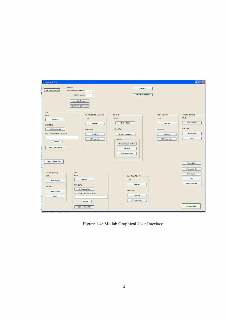
Figure 1.4: Matlab Graphical User Interface
12

Figure 1.5: GUI: Load Default Values Window
13

Chapter 2
Ideal Simulation
2.1 Component Modules
For a baseline comparison of the cross-correlation and Doppler plots in the waveform diversity
study, an ideal simulation is needed. The ideal simulation shows the cross-correlation and range-
Doppler response of the radar system if the system is in a sense, perfect. Throughout this document,
the terms “ideal” and “baseline” simulation are used interchangeably. Both refer to the simulation
where all components are ideal. The ideal components do not have any nonlinearities that effect the
output of the component. In order that the component models are easy to manipulate and modify, a
separate module is constructed for each component. This allows for easy modification of any and all
of the component parameters. Associated with each component module are default values for each
of the parameters. Every parameter can be modified such that the component satisfies the system
requirements.
2.1.1 Waveform Generator
Phase-coded waveforms were used to develop this simulation. The waveform generation module
allows for control over parameters such as waveform selection and timing on a pulse-to-pulse and
channel-to-channel basis. In execution of the ideal waveform generation module, the output code
length, number of phases, chip rate, integration time, and pulse repetition frequency can all be
altered. The chip rate is defined as the inverse of the length of the pulse. The units of chip rate
14

are Hertz. Both the integration time and the pulse repetition frequency are used in determining the
number of pulses available for integration as shown in Equation 1.1. Table 2.1 shows the default
parameters used in the ideal waveform generator module.
Table 2.1: Ideal Waveform Generator
Parameter Value
Number of phases 2
Code length 10
Chip rate 750 kHz
Integration Time 75 ms
Pulse Repetition Frequency 500 Hz
The simulation also has the ability to simulate multiple frequency branches. There is a block
in the GUI that allows control over the number of branches used. In this block, the total number of
branches can be specified by the user. The IF frequency corresponding to each branch is also a user
input in this block.
2.1.2 Frequency Modulation
In the transmit chain of the end-to-end radar system simulation, two frequency modulations take
place. The first is to the respective IF frequency of each branch and the other is a modulation of the
summed IF signals to the RF frequency, illustrated by
SIF,out(t) = SI,in(t) cos(2πfIF t) + SQ,in(t) sin(2πfIF t) (2.1)
and
SRF,out(t) = SIF,in(t) cos(2π(fRF − fIF )t), (2.2)
respectively. On receive, the signal is demodulated twice, once down from the RF to the IF fre-
quency, and the other to baseband from the respective IF frequencies of that branch. An ideal mixer
module is created for the analog modulation, or the modulation to the RF frequency. An ideal mixer
is, mathematically, the signal multiplied by a sinusoidal waveform [27]. The ideal mixer module
allows for the user to change the carrier frequency of modulation. Table 2.2 shows the default
parameters chosen for both the IF and RF modulations.
15
Table 2.2: Ideal Frequency Modulation
Frequency Parameter Value
Branch 1 200 MHz
Intermediate Frequency Branch 2 300 MHz
Branch 3 400 MHz
RF Frequency 2 GHz
2.1.3 Amplifier
An amplifier is used to increase the power of a signal. The radar signal in the end-to-end simulation
goes through an amplifier on both the transmit and receive chains. The signal gets amplified on
transmit right before it is transmitted. The signal gets amplified a second time right after it is
received. A module was created to simulate the amplifier. The ideal amplifier does not take noise
into consideration in the output signal. The ideal amplifier simply scales the input signal [21]. The
governing equation for an ideal amplifier is given by
Sout(t) = aSin(t) (2.3)
where a is a scalar quantity.
2.1.4 Converters
Digital-to-Analog Converter
An ideal digital-to-analog converter is simply modeled as an upsampler. To simulate the conversion
from a digital signal to an analog signal, the signal is upsampled to a rate of ten times the Nyquist
rate of the RF frequency. The Nyquist rate is defined as the value of two times the highest frequency
component. Ten times the Nyquist rate of the RF frequency is used because, after the digital-to-
analog conversion, the RF frequency is the carrier for the signal throughout the rest of the simulation.
Therefore, to insure that the signal is heavily upsampled and aliasing due to nonlinearities does not
occur, the analog sampling rate is chosen to be ten times the Nyquist of the carrier frequency. Since
the analog sampling rate is dependent upon the RF frequency, the only user input to the ideal DAC
16

module is the RF frequency. The frequency modulation table, Table 2.2 shows the value chosen for
the RF frequency.
Analog-to-Digital Converter
An analog-to-digital converter is the component that does just the opposite of the DAC. The ADC
converts an analog signal to a digital signal. An ideal ADC is modeled just the opposite of the DAC
also. It is modeled as a downsampler which converts analog sampling rate to the much lower digital
sampling rate. Since the analog sampling rate is defined in the DAC module, and the digital rate is
the original rate of sample preceding the digital-to-analog converter, there are no user inputs to the
ideal ADC module.
2.1.5 Time Delay Network
The time delay network block consists of mainly the target properties. This block simulates the
target interaction and signal return. The radar simulation has the capability to simulate a stationary
point target as well as a moving point target. Therefore, the target properties specified by the user
in the ideal time delay network module are the reference range, target range, range swath, target
velocity, and signal amplitude. The reference range is the range to the center of the range swath,
a range at which the time delay is known. The target range is the range at which the target lies.
The range swath is the area on the ground that the radar can see. The target velocity is, as its name
indicates, the velocity of the target. Table 2.3 shows the chosen target parameters for the ideal radar
simulation. The time delay network block can easily be extended to simulate a phased array. The
phased array allows for the study of beamforming or spatial filtering, etc.
2.2 Software Testing
2.2.1 Simulation
Before the ideal simulation is begun, the waveform generater module is used to input the pulse
repetition frequency and the integration time required for the simulation. Once the user inputs these
17
Table 2.3: Ideal Time Delay Network
Parameter Value
Target Range 9.75 km
Reference Range 10 km
Range Swath 1 km
Target Velocity 0 ms
Signal Amplitude 1
values, the number of pulses is calculated according to Equation 1.1. The integration time and pulse
repetition frequency used in this ideal simulation are given in Table 2.1. The number of pulses
needed based upon these values was found to be 38. Please note that the following description of
the ideal simulation shows plots only from the first pulse generation. The plot of the detection cross-
correlation is of only the first pulse also. Not until the Doppler shift is plotted are all the generated
pulses used.
When the ideal simulation is begun, the number of frequency branches and their respective
frequencies are chosen. Recall that the transmit architecture is shown in Figure 1.1. In this baseline
simulation, three branches are used with the IF frequencies shown in Table 2.2. Once the number
of branches and frequencies are chose, a waveform for each branch is generated. The waveform
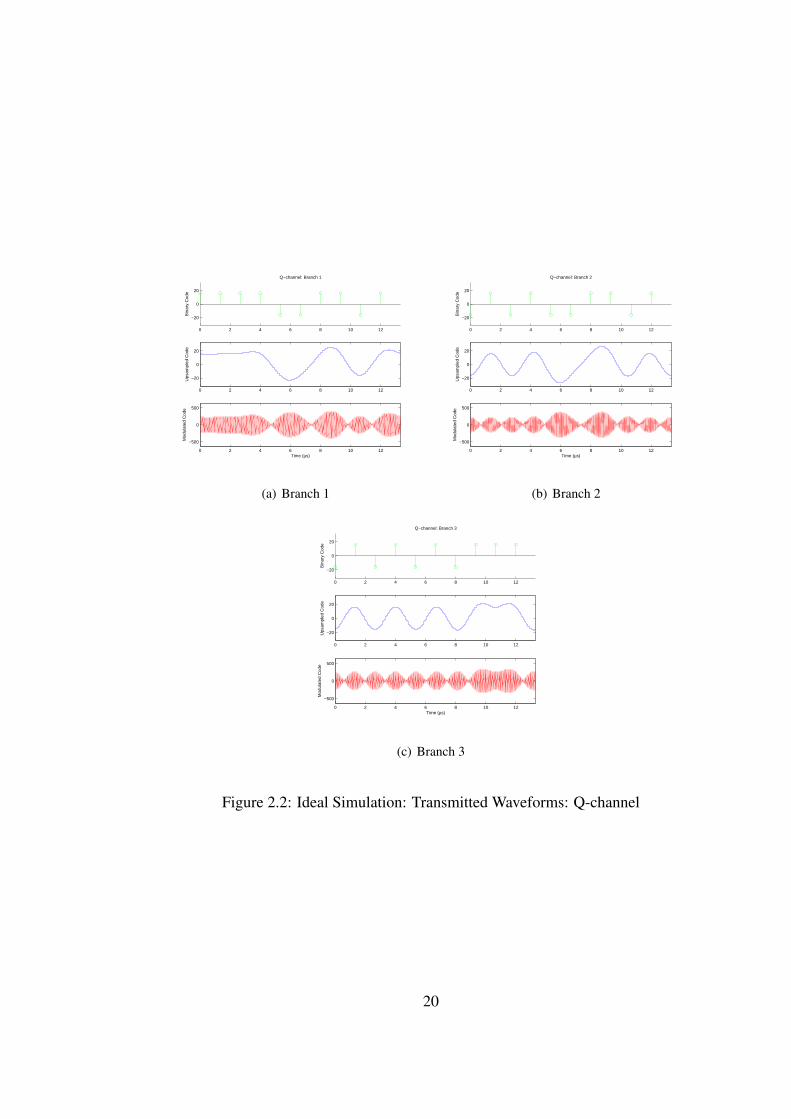
generation module is used to generate a binary I- and Q-channel phase code for the three branches.
The first plots in Figure 2.1 show the binary phase code for each of the three branches for the
I-channel while the first plots in Figure 2.2 show the binary phase code for the Q-channel.
After the waveform generation, the binary signals get upsampled and modulated up to their
respective IF brands. The intermediate frequencies for each branch, from Table 2.2 are 200 MHz,
300 MHz, and 400 MHz. The second and third plots in Figures 2.1 and 2.2 show the upsampled
code and the IF modulated code for both the I- and the Q-channel, respectively.
The next step according to Figure 1.1 is a summation of the complex signals. The IF modulated
I- and Q-channel for each branch are summed. Then the signals are summed over all of the branches
such that only one signal is transmitted. The summed signal that is to propagate throughout the rest
of the simulation is shown in Figure 2.3 while its frequency spectrum is shown in Figure 2.4.
The entire simulation to this point has been done digitally. The signal now needs to be con-
18

0 2 4 6 8 10 12
−20
0
20
Bin
ary
Cod
e
I−channel: Branch 1
0 2 4 6 8 10 12
−20
0
20
Ups
ampl
ed C
ode
0 2 4 6 8 10 12
−500
0
500
Mod
ulat
ed C
ode
Time (µs)
(a) Branch 1
0 2 4 6 8 10 12
−20
0
20
Bin
ary
Cod
e
I−channel: Branch 2
0 2 4 6 8 10 12
−20
0
20
Ups
ampl
ed C
ode
0 2 4 6 8 10 12
−500
0
500
Mod
ulat
ed C
ode
Time (µs)
(b) Branch 2
0 2 4 6 8 10 12
−20
0
20
Bin
ary
Cod
e
I−channel: Branch 3
0 2 4 6 8 10 12
−20
0
20
Ups
ampl
ed C
ode
0 2 4 6 8 10 12
−500
0
500
Mod
ulat
ed C
ode
Time (µs)
(c) Branch 3
Figure 2.1: Ideal Simulation: Transmitted Waveforms: I-channel
19
0 2 4 6 8 10 12
−20
0
20
Bin
ary
Cod
e
Q−channel: Branch 1
0 2 4 6 8 10 12
−20
0
20
Ups
ampl
ed C
ode
0 2 4 6 8 10 12
−500
0
500
Mod
ulat
ed C
ode
Time (µs)
(a) Branch 1
0 2 4 6 8 10 12
−20
0
20
Bin
ary
Cod
e
Q−channel: Branch 2
0 2 4 6 8 10 12
−20
0
20
Ups
ampl
ed C
ode
0 2 4 6 8 10 12
−500
0
500
Mod
ulat
ed C
ode
Time (µs)
(b) Branch 2
0 2 4 6 8 10 12
−20
0
20
Bin
ary
Cod
e
Q−channel: Branch 3
0 2 4 6 8 10 12
−20
0
20
Ups
ampl
ed C
ode
0 2 4 6 8 10 12
−500
0
500
Mod
ulat
ed C
ode
Time (µs)
(c) Branch 3
Figure 2.2: Ideal Simulation: Transmitted Waveforms: Q-channel
20

0 2 4 6 8 10 12 14−1000
−800
−600
−400
−200
0
200
400
600
800
1000
Sum
med
Sig
nal
Time (µs)
Summed Digital Signal
Figure 2.3: Ideal Simulation: Summation of digital signals from all three branches
21

0 50 100 150 200 250 300 350 400 4500
20
40
60
80
100
120
140Summed Digital Signal Spectrum
Frequency (MHz)
Figure 2.4: Ideal Simulation: Frequency spectrum of summed signal
22
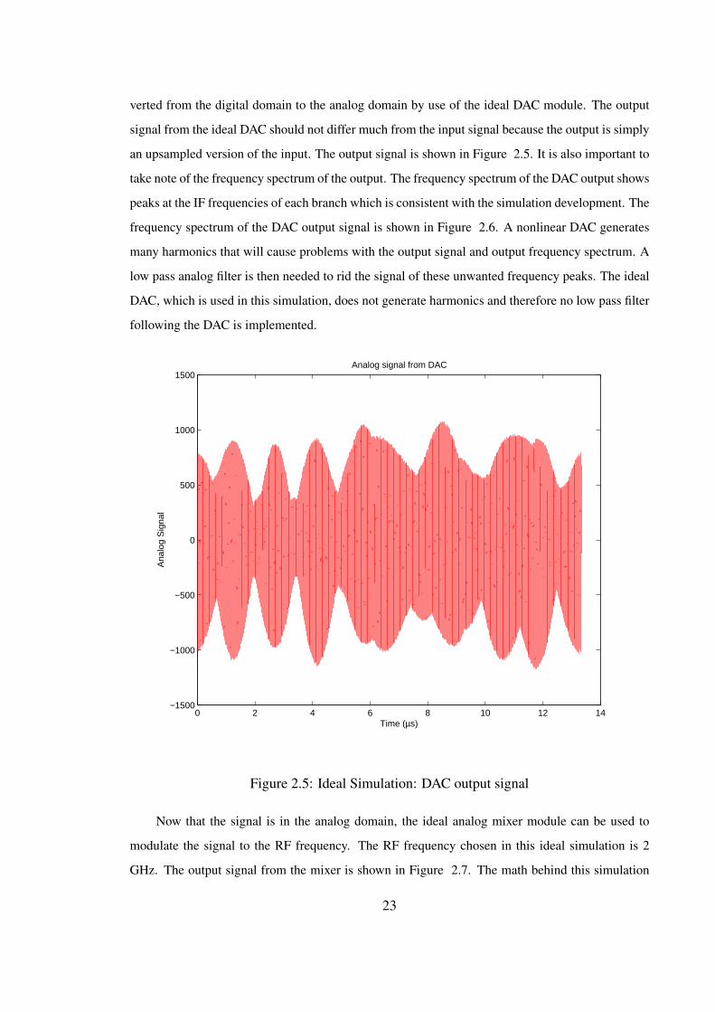
verted from the digital domain to the analog domain by use of the ideal DAC module. The output
signal from the ideal DAC should not differ much from the input signal because the output is simply
an upsampled version of the input. The output signal is shown in Figure 2.5. It is also important to
take note of the frequency spectrum of the output. The frequency spectrum of the DAC output shows
peaks at the IF frequencies of each branch which is consistent with the simulation development. The
frequency spectrum of the DAC output signal is shown in Figure 2.6. A nonlinear DAC generates
many harmonics that will cause problems with the output signal and output frequency spectrum. A
low pass analog filter is then needed to rid the signal of these unwanted frequency peaks. The ideal
DAC, which is used in this simulation, does not generate harmonics and therefore no low pass filter
following the DAC is implemented.
0 2 4 6 8 10 12 14−1500
−1000
−500
0
500
1000
1500
Ana
log
Sig
nal
Time (µs)
Analog signal from DAC
Figure 2.5: Ideal Simulation: DAC output signal
Now that the signal is in the analog domain, the ideal analog mixer module can be used to
modulate the signal to the RF frequency. The RF frequency chosen in this ideal simulation is 2
GHz. The output signal from the mixer is shown in Figure 2.7. The math behind this simulation
23
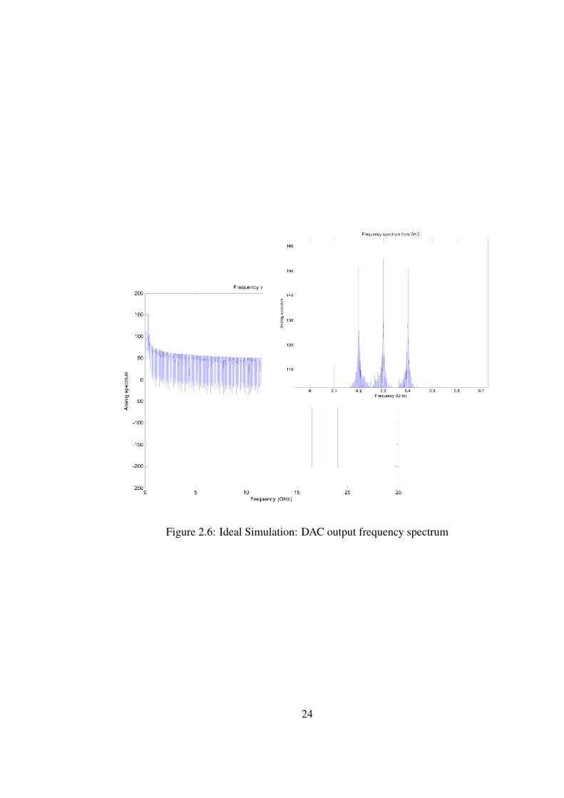
Figure 2.6: Ideal Simulation: DAC output frequency spectrum
24
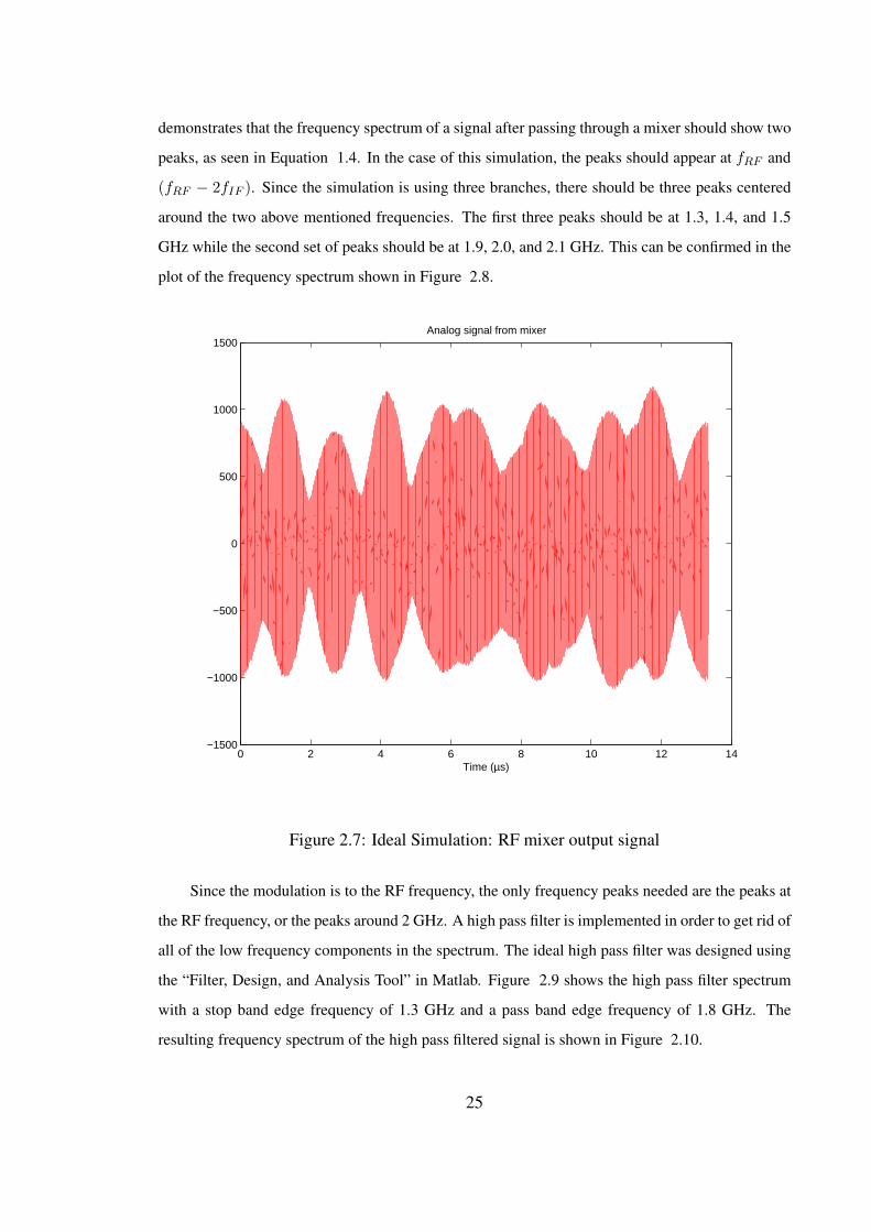
demonstrates that the frequency spectrum of a signal after passing through a mixer should show two
peaks, as seen in Equation 1.4. In the case of this simulation, the peaks should appear at fRF and
(fRF − 2fIF ). Since the simulation is using three branches, there should be three peaks centered
around the two above mentioned frequencies. The first three peaks should be at 1.3, 1.4, and 1.5
GHz while the second set of peaks should be at 1.9, 2.0, and 2.1 GHz. This can be confirmed in the
plot of the frequency spectrum shown in Figure 2.8.
0 2 4 6 8 10 12 14−1500
−1000
−500
0
500
1000
1500
Time (µs)
Analog signal from mixer
Figure 2.7: Ideal Simulation: RF mixer output signal
Since the modulation is to the RF frequency, the only frequency peaks needed are the peaks at
the RF frequency, or the peaks around 2 GHz. A high pass filter is implemented in order to get rid of
all of the low frequency components in the spectrum. The ideal high pass filter was designed using
the “Filter, Design, and Analysis Tool” in Matlab. Figure 2.9 shows the high pass filter spectrum
with a stop band edge frequency of 1.3 GHz and a pass band edge frequency of 1.8 GHz. The
resulting frequency spectrum of the high pass filtered signal is shown in Figure 2.10.
25
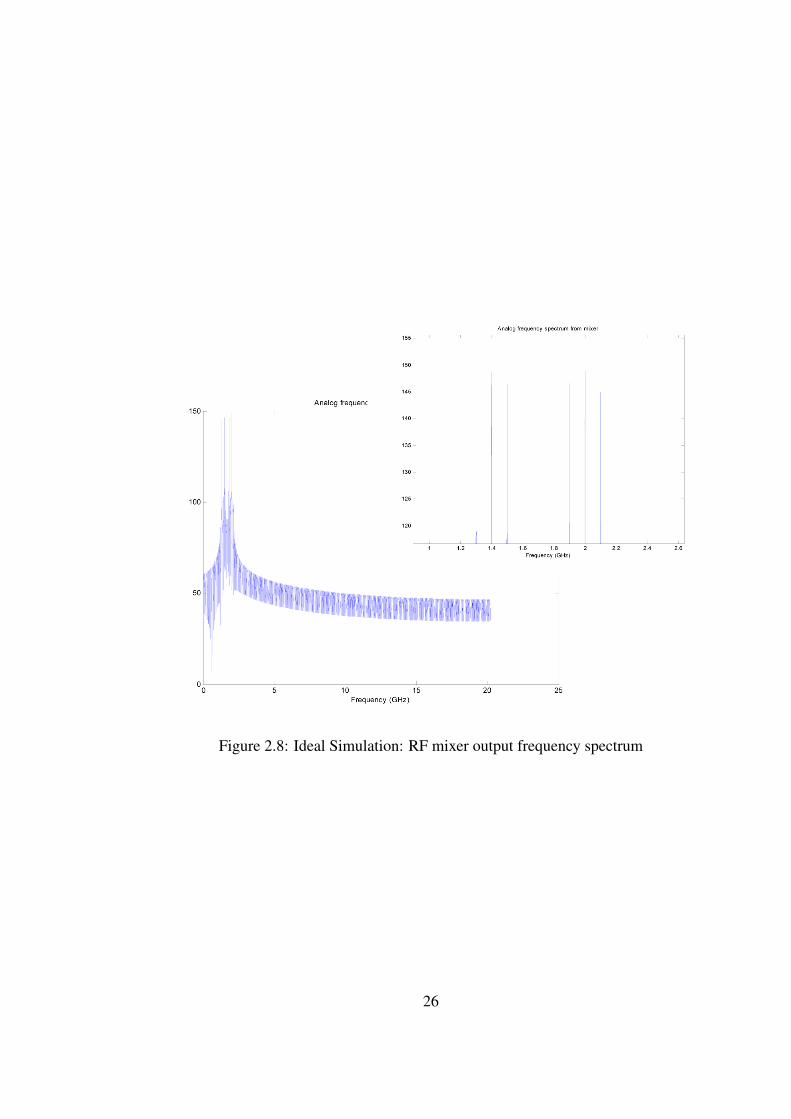
Figure 2.8: Ideal Simulation: RF mixer output frequency spectrum
26

0 5 10 15 20 25−120
−100
−80
−60
−40
−20
0
20
Frequency (GHz)
HP
F R
espo
nse
HPF frequency response
Figure 2.9: Ideal Simulation: High pass filter spectrum of filter following RF mixer
27
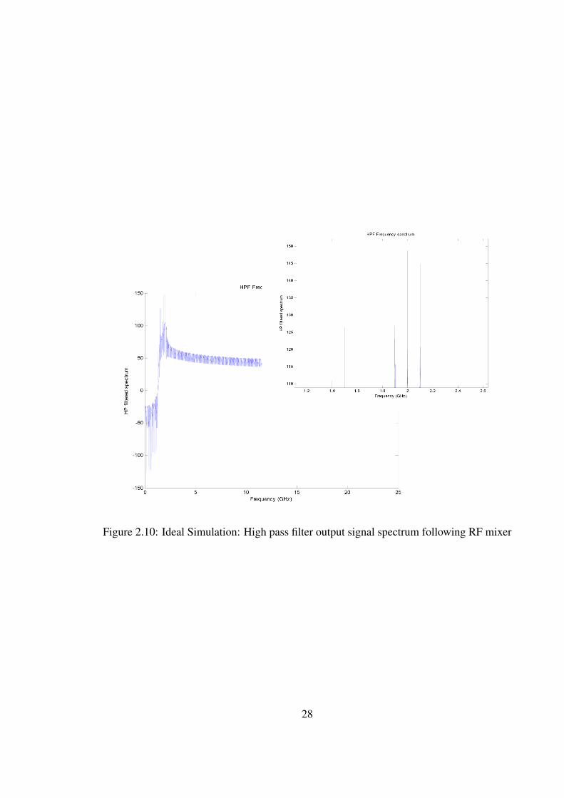
Figure 2.10: Ideal Simulation: High pass filter output signal spectrum following RF mixer
28
In reference again to the system architecture in Figure 1.1, the final step before the signal
is transmitted is an amplifier. Since this simulation is using all ideal components, there is need
to change the signal amplitude to suit the specifications of the component following the amplifier.
Therefore, there is no need for an amplifier in this baseline simulation.
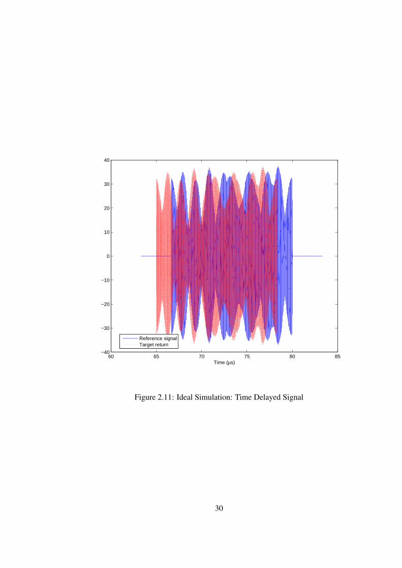
After the signal passes through the entire transmit system architecture, it is delayed upon re-
turn. The time delay of the signal is based upon the range and velocity of the point target. These
parameters are chosen by the user, specified in the target delay module, and for this simulation, have
the values given in Table 2.3. The actual target range is calculated using
R(τ) = R0 + vtτk (2.4)
where R0 is the user input target range, vt is the user input target velocity, and τk is the time at
which the signal pulse is transmitted.
The following equation
t0(τ) =2R(τ)
c(2.5)
is used to calculate the time delay of the signal where R(τ) is the range previously calculated and c
is the speed of light, which is 300, 000, 000ms . The target used in this simulation is a stationary point
target. Since the target velocity is zero, the actual target range is simply the target range chosen by
the user. Using the speed of light and the target range, the time delay for this simulation is calculated
to be 65µs. Figure 2.11 is a plot of both the transmitted signal and the delayed signal at the center
of the range swath.
After the signal is received, an amplifier is again needed to change the received signal ampli-
tude. Again, this is an ideal simulation, so there is no need to change the amplitude for the com-
ponents following the amplifier. Therefore, the amplifier is simply a placeholder in this baseline
simulation.
The signal upon receive is still at RF frequency. The received signal should be converted to
baseband. The first demodulation to take place, according to the receive architecture in Figure 1.2 is
the modulation down from the RF frequency. The analog mixer module is used for the demodulation
process. The demodulated signal is shown in Figure 2.12 while the frequency spectrum of the signal
is shown in Figure 2.13. According to the mathematical derivation and Equation 1.7, the frequency
spectrum of the signal should have peaks at (2fRF − fIF ) and fIF . Since this ideal simulation
29
60 65 70 75 80 85−40
−30
−20
−10
0
10
20
30
40
Time (µs)
Reference signalTarget return
Figure 2.11: Ideal Simulation: Time Delayed Signal
30

is using three frequency channels, there should be three peaks at the higher frequencies, that is
2fRF minus each one of the IF frequencies, and three peaks at each of the IF frequencies. The
plot of the frequency spectrum is consistent with the mathematical theory. Figure 2.13 shows the
entire frequency spectrum of the RF demodulated signal, with emphasis on both the low and high
frequency peaks. The peaks are at the expected frequencies.
0 5 10 15 20 25−40
−30
−20
−10
0
10
20
30
40
Time (µs)
Analog signal from mixer
Figure 2.12: Ideal Simulation: RF demodulation output signal
Due to the fact that RF demodulation brought the signal to the IF frequency range, the only
peaks to be concerned with are the low frequency peaks. Therefore, a low pass filter is needed to
suppress the high frequency signal. The ideal low pass filter does not take into consideration noise
or losses inside the component. The ideal filter was again designed using the “Filter, Design, and
Analysis Tool” in Matlab. The low pass filter has a pass band edge frequency of 500 MHz and a
stop band edge frequency of 800 MHz, as seen in the filter frequency spectrum in Figure 2.14. The
resulting frequency spectrum of the output of the low pass filter is shown in Figure 2.15.
31

Figure 2.13: Ideal Simulation: RF demodulation output frequency spectrum
32

0 5 10 15 20 25−120
−100
−80
−60
−40
−20
0
20
Frequency (GHz)
LPF
Res
pons
e
First LPF Rx Response
Figure 2.14: Ideal Simulation: Low pass filter spectrum of filter following RF demodula-
tion on receive
33

0 5 10 15 20 25−200
−150
−100
−50
0
50
100
150
LP fi
ltere
d sp
ectr
um
Frequency (GHz)
First LPF Rx frequency response
Figure 2.15: Ideal Simulation: Low pass filter output frequency spectrum following RF
demodulation on receive
34
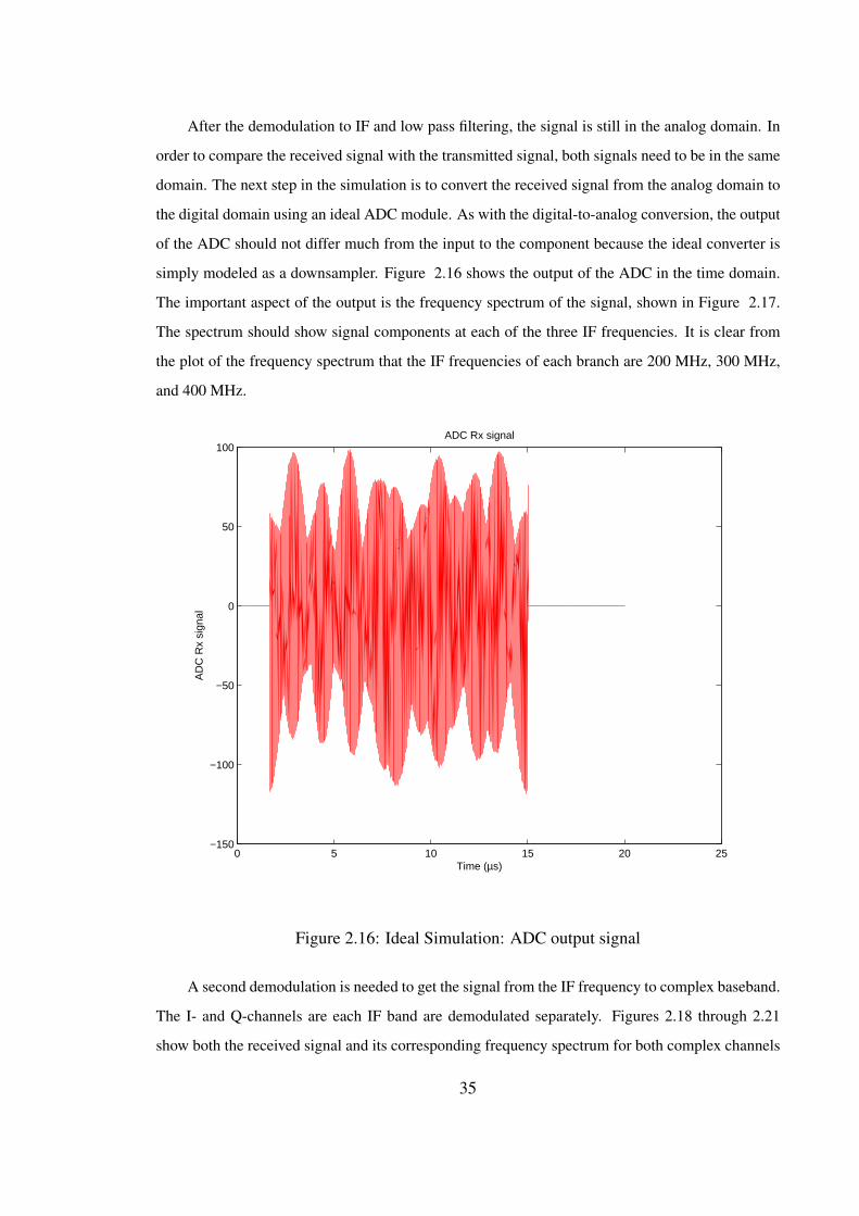
After the demodulation to IF and low pass filtering, the signal is still in the analog domain. In
order to compare the received signal with the transmitted signal, both signals need to be in the same
domain. The next step in the simulation is to convert the received signal from the analog domain to
the digital domain using an ideal ADC module. As with the digital-to-analog conversion, the output
of the ADC should not differ much from the input to the component because the ideal converter is
simply modeled as a downsampler. Figure 2.16 shows the output of the ADC in the time domain.
The important aspect of the output is the frequency spectrum of the signal, shown in Figure 2.17.
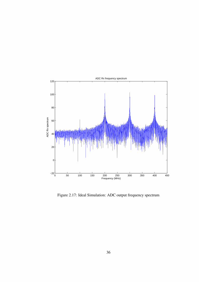
The spectrum should show signal components at each of the three IF frequencies. It is clear from
the plot of the frequency spectrum that the IF frequencies of each branch are 200 MHz, 300 MHz,
and 400 MHz.
0 5 10 15 20 25−150
−100
−50
0
50
100
AD
C R
x si
gnal
Time (µs)
ADC Rx signal
Figure 2.16: Ideal Simulation: ADC output signal
A second demodulation is needed to get the signal from the IF frequency to complex baseband.
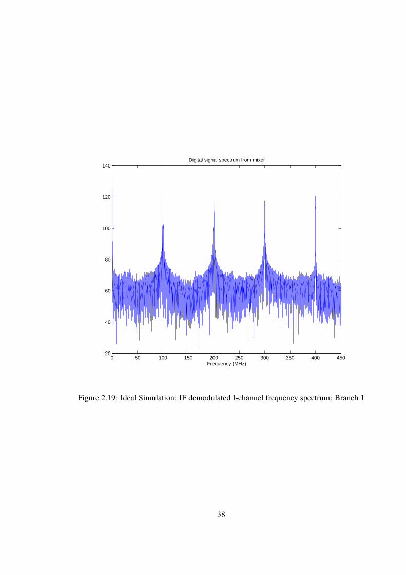
The I- and Q-channels are each IF band are demodulated separately. Figures 2.18 through 2.21
show both the received signal and its corresponding frequency spectrum for both complex channels
35
0 50 100 150 200 250 300 350 400 450−20
0
20
40
60
80
100
120
AD
C R
x sp
ectr
um
Frequency (MHz)
ADC Rx frequency spectrum
Figure 2.17: Ideal Simulation: ADC output frequency spectrum
36

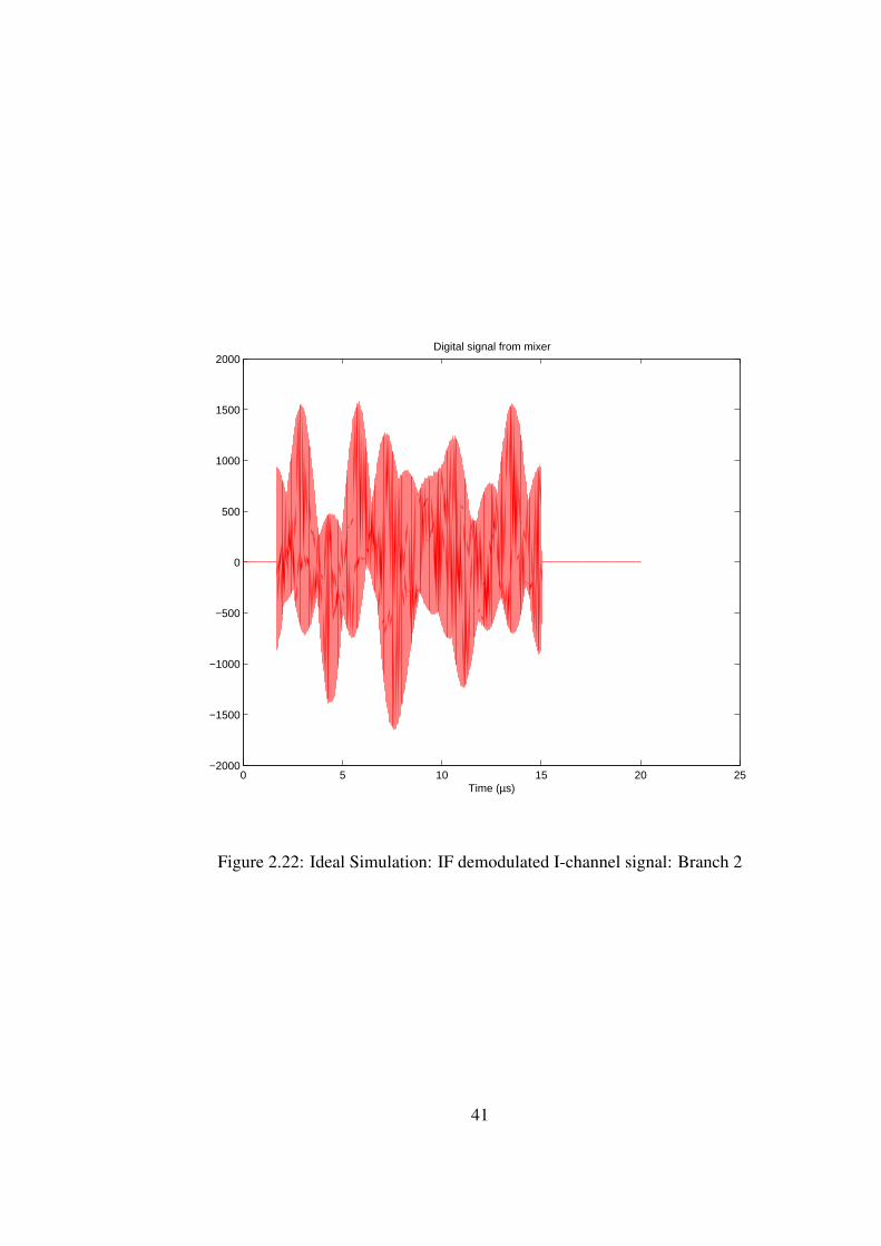
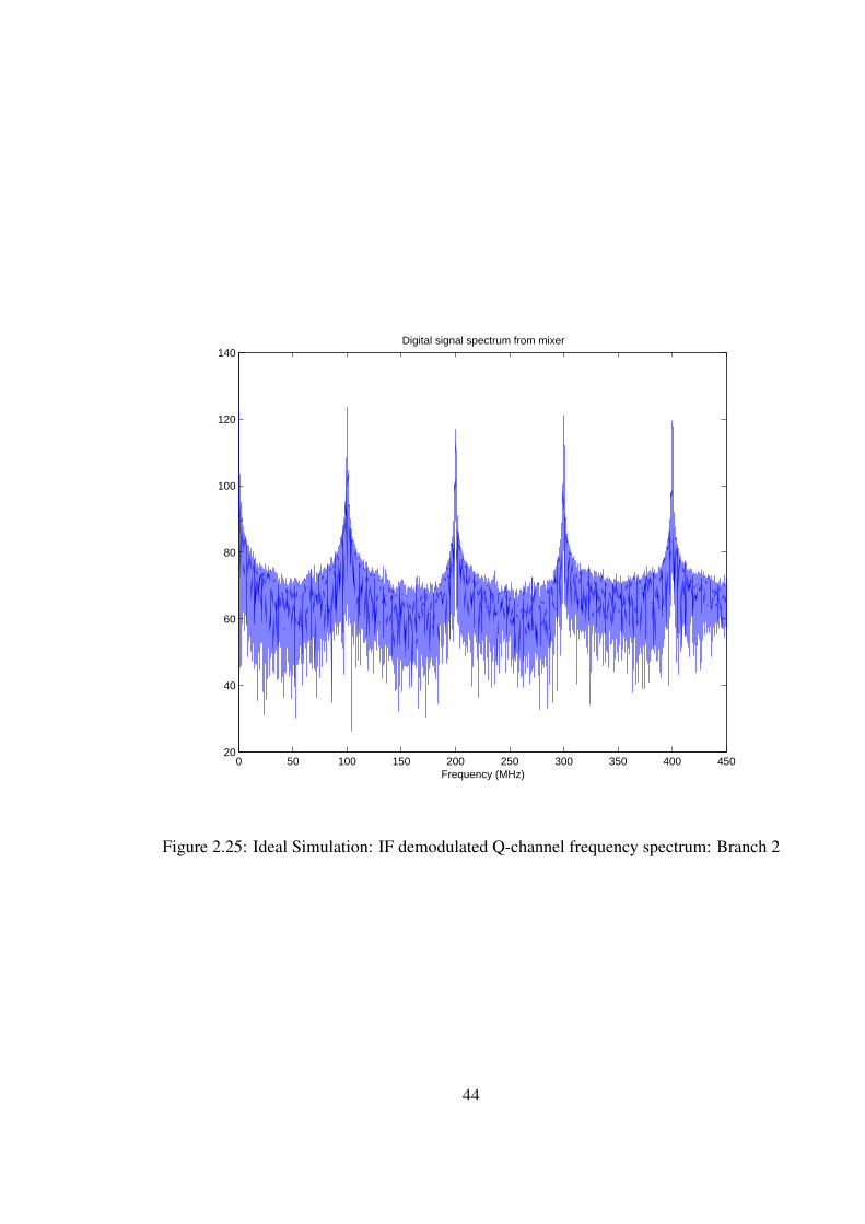
of branch one. Figures 2.22 through 2.25 and Figures 2.26 through 2.29 show the same plots for
branches two and three, respectively.
0 5 10 15 20 25−1500
−1000
−500
0
500
1000
1500
2000
Time (µs)
Digital signal from mixer
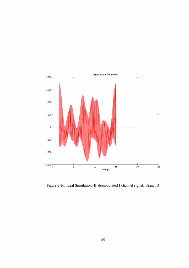
Figure 2.18: Ideal Simulation: IF demodulated I-channel signal: Branch 1
In examination of the plots of the signal frequency spectrum for both complex channels, the
modulation process generated unwanted harmonics in the frequency spectrum of the complex output
signal for every branch. A low pass filter is needed to filter out these unwanted frequency peaks in
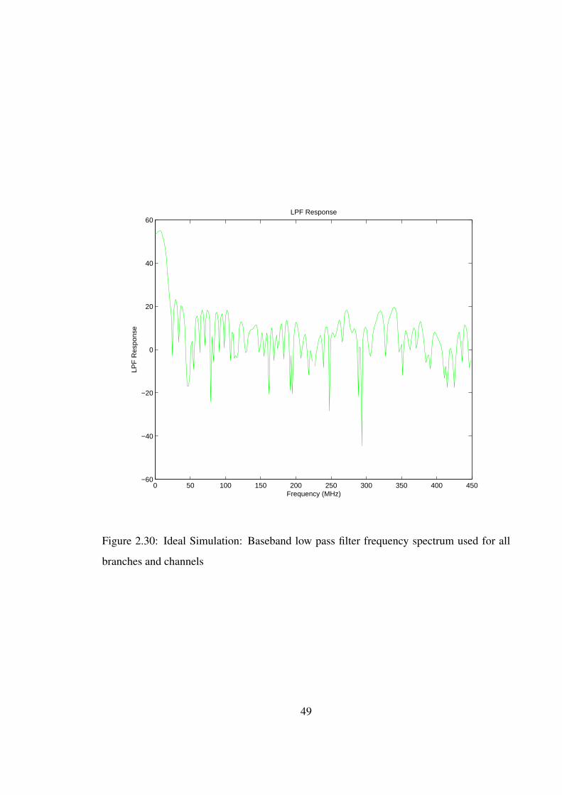
the spectrums. The received signal should also be at baseband. Figure 2.30 shows the frequency
response of the low pass filter used for the complex channels in every branch. The signal spectrum
after filtering remains the same for all channels in that there is a single peak at baseband. The
filtered signal spectrum for the I-channel of the first branch can be seen in Figure 2.31. Note that all
unwanted harmonics were filtered out leaving only the peak at baseband.
The above described simulation is similar for stationary targets as well as moving targets.
Please note that the results section of this chapter, immediately following, addresses the stationary
37
0 50 100 150 200 250 300 350 400 45020
40
60
80
100
120
140Digital signal spectrum from mixer
Frequency (MHz)
Figure 2.19: Ideal Simulation: IF demodulated I-channel frequency spectrum: Branch 1
38

0 5 10 15 20 25−1500
−1000
−500
0
500
1000
1500
2000
Time (µs)
Digital signal from mixer
Figure 2.20: Ideal Simulation: IF demodulated Q-channel signal: Branch 1
39

0 50 100 150 200 250 300 350 400 45020
40
60
80
100
120
140Digital signal spectrum from mixer
Frequency (MHz)
Figure 2.21: Ideal Simulation: IF demodulated Q-channel frequency spectrum: Branch 1
40
0 5 10 15 20 25−2000
−1500
−1000
−500
0
500
1000
1500
2000
Time (µs)
Digital signal from mixer
Figure 2.22: Ideal Simulation: IF demodulated I-channel signal: Branch 2
41

0 50 100 150 200 250 300 350 400 45020
40
60
80
100
120
140Digital signal spectrum from mixer
Frequency (MHz)
Figure 2.23: Ideal Simulation: IF demodulated I-channel frequency spectrum: Branch 2
42

0 5 10 15 20 25−1500
−1000
−500
0
500
1000
1500
2000
Time (µs)
Digital signal from mixer
Figure 2.24: Ideal Simulation: IF demodulated Q-channel signal: Branch 2
43
0 50 100 150 200 250 300 350 400 45020
40
60
80
100
120
140Digital signal spectrum from mixer
Frequency (MHz)
Figure 2.25: Ideal Simulation: IF demodulated Q-channel frequency spectrum: Branch 2
44
0 5 10 15 20 25−1500
−1000
−500
0
500
1000
1500
2000
Time (µs)
Digital signal from mixer
Figure 2.26: Ideal Simulation: IF demodulated I-channel signal: Branch 3
45

0 50 100 150 200 250 300 350 400 45020
40
60
80
100
120
140Digital signal spectrum from mixer
Frequency (MHz)
Figure 2.27: Ideal Simulation: IF demodulated I-channel frequency spectrum: Branch 3
46

0 5 10 15 20 25−1500
−1000
−500
0
500
1000
1500
2000
Time (µs)
Digital signal from mixer
Figure 2.28: Ideal Simulation: IF demodulated Q-channel signal: Branch 3
47

0 50 100 150 200 250 300 350 400 45020
40
60
80
100
120
140Digital signal spectrum from mixer
Frequency (MHz)
Figure 2.29: Ideal Simulation: IF demodulated Q-channel frequency spectrum: Branch 3
48
0 50 100 150 200 250 300 350 400 450−60
−40
−20
0
20
40
60
Frequency (MHz)
LPF
Res
pons
e
LPF Response
Figure 2.30: Ideal Simulation: Baseband low pass filter frequency spectrum used for all
branches and channels
49

0 50 100 150 200 250 300 350 400 450−20
0
20
40
60
80
100
sOut
spe
ctru
m
Frequency (MHz)
LPF signal frequency spectrum
Figure 2.31: Ideal Simulation: Received signal spectrum after low pass filter to remove
harmonics
50
target detection as well as moving target detection. The difference between stationary and moving
targets is noticeable in the analysis of the range-Doppler plots since a moving target causes Doppler
shift.
2.2.2 Results
Cross-correlation
Once the baseband signal is received, a cross-correlation of the transmitted pulse with the received
pulse can be performed. Since the signals are complex, the cross-correlation is complex also. The
cross-correlation plot should peak at the time delay of the signal. Looking back, the theoretical time
delay for this ideal simulation was calculated to be 65µs. Figure 2.32 shows the cross-correlation
plot for each of the three branches. Within the figure contains the time delay value extracted from
the peak of the cross-correlation plots. The simulated time delays are 64.887µs, 64.881µs, and
64.883µs for pulse number one of branches one, two, and three, respectively.
Doppler
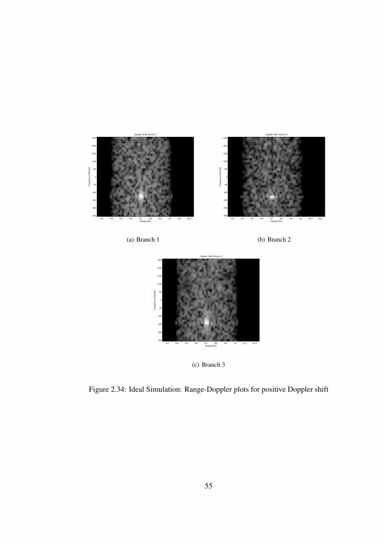
Once all of the 38 pulses are generated, received, and detected, a range-Doppler plot can be pro-
duced. The range-Doppler plot should show a peak value at the range of the target and the correct
Doppler frequency shift. Figure 2.33 shows the plots for each of the three branches. Since the
target is stationary, there should be no Doppler shift. The range was specified by the user in the
target delay module, and for this simulation had the value of 9.75 km. It can be seen that in each of
the range-Doppler plots, the peak is at 0 Hz Doppler shift and a range of 9.75 km, as predicted.
After the range-Doppler plots are generated, calculations of the side lobe levels of each of the
plots are performed. A table of the calculated values for both the range and the Doppler shift are
shown in Table 2.4.
The ideal simulation was run again, but this time with a moving target. The target was given a
positive velocity of 10ms , input into the target delay module. Range-Doppler plots for the moving
target were generated along with the main lobe and side lobe calculations. The peak of the range-
Doppler plot with a moving target of specified velocity should now be at 133 Hz, according to
Equation 1.17 where the frequency used to calculate the wavelength is RF, or 2 GHz. This is true
51

45 50 55 60 65 70 75 80 85 900
1
2
3
4
5
6
7x 10
12
Lag time (µs)
Cro
ss−
corr
elat
ion
Cross−correlation
Time Delay: 64.888 µs
(a) Branch 1
45 50 55 60 65 70 75 80 85 900
2
4
6
8
10
12x 10
12
Lag time (µs)C
ross
−co
rrel
atio
n
Cross−correlation
Time Delay: 64.888 µs
(b) Branch 2
45 50 55 60 65 70 75 80 85 900
1
2
3
4
5
6
7
8x 10
12
Lag time (µs)
Cro
ss−
corr
elat
ion
Cross−correlation
Time Delay: 64.887 µs
(c) Branch 3
Figure 2.32: Ideal Simulation: Cross-correlation
52

Doppler Shift: Branch 1
Fre
quen
cy s
hift
(Hz)
Range (km)9.3 9.4 9.5 9.6 9.7 9.8 9.9 10 10.1 10.2
−250
−200
−150
−100
−50
0
50
100
150
200
250
(a) Branch 1
Doppler Shift: Branch 2
Fre
quen
cy s
hift
(Hz)
Range (km)9.3 9.4 9.5 9.6 9.7 9.8 9.9 10 10.1 10.2
−250
−200
−150
−100
−50
0
50
100
150
200
250
(b) Branch 2
Doppler Shift: Branch 3
Fre
quen
cy s
hift
(Hz)
Range (km)9.3 9.4 9.5 9.6 9.7 9.8 9.9 10 10.1 10.2
−250
−200
−150
−100
−50
0
50
100
150
200
250
(c) Branch 3
Figure 2.33: Ideal Simulation: Range-Doppler plots for zero Doppler shift
53
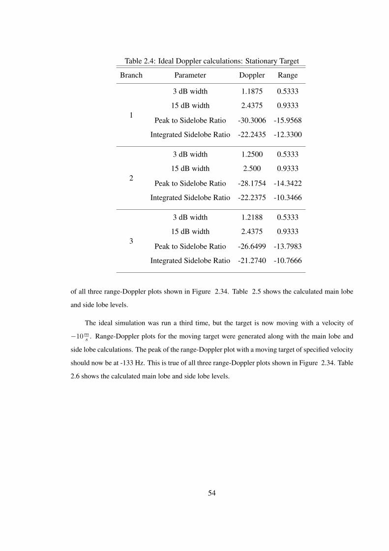
Table 2.4: Ideal Doppler calculations: Stationary Target
Branch Parameter Doppler Range
3 dB width 1.1875 0.5333
15 dB width 2.4375 0.93331
Peak to Sidelobe Ratio -30.3006 -15.9568
Integrated Sidelobe Ratio -22.2435 -12.3300
3 dB width 1.2500 0.5333
15 dB width 2.500 0.93332
Peak to Sidelobe Ratio -28.1754 -14.3422
Integrated Sidelobe Ratio -22.2375 -10.3466
3 dB width 1.2188 0.5333
15 dB width 2.4375 0.93333
Peak to Sidelobe Ratio -26.6499 -13.7983
Integrated Sidelobe Ratio -21.2740 -10.7666
of all three range-Doppler plots shown in Figure 2.34. Table 2.5 shows the calculated main lobe
and side lobe levels.
The ideal simulation was run a third time, but the target is now moving with a velocity of
−10ms . Range-Doppler plots for the moving target were generated along with the main lobe and
side lobe calculations. The peak of the range-Doppler plot with a moving target of specified velocity
should now be at -133 Hz. This is true of all three range-Doppler plots shown in Figure 2.34. Table
2.6 shows the calculated main lobe and side lobe levels.
54
Doppler Shift: Branch 1
Fre
quen
cy s
hift
(Hz)
Range (km)9.3 9.4 9.5 9.6 9.7 9.8 9.9 10 10.1 10.2
−250
−200
−150
−100
−50
0
50
100
150
200
250
(a) Branch 1
Doppler Shift: Branch 2
Fre
quen
cy s
hift
(Hz)
Range (km)9.3 9.4 9.5 9.6 9.7 9.8 9.9 10 10.1 10.2
−250
−200
−150
−100
−50
0
50
100
150
200
250
(b) Branch 2
Doppler Shift: Branch 3
Fre
quen
cy s
hift
(Hz)
Range (km)9.3 9.4 9.5 9.6 9.7 9.8 9.9 10 10.1 10.2
−250
−200
−150
−100
−50
0
50
100
150
200
250
(c) Branch 3
Figure 2.34: Ideal Simulation: Range-Doppler plots for positive Doppler shift
55

Doppler Shift: Branch 1
Fre
quen
cy s
hift
(Hz)
Range (km)9.3 9.4 9.5 9.6 9.7 9.8 9.9 10 10.1 10.2
−250
−200
−150
−100
−50
0
50
100
150
200
250
(a) Branch 1
Doppler Shift: Branch 2
Fre
quen
cy s
hift
(Hz)
Range (km)9.3 9.4 9.5 9.6 9.7 9.8 9.9 10 10.1 10.2
−250
−200
−150
−100
−50
0
50
100
150
200
250
(b) Branch 2
Doppler Shift: Branch 3
Fre
quen
cy s
hift
(Hz)
Range (km)9.3 9.4 9.5 9.6 9.7 9.8 9.9 10 10.1 10.2
−250
−200
−150
−100
−50
0
50
100
150
200
250
(c) Branch 3
Figure 2.35: Ideal Simulation: Range-Doppler plots for negative Doppler shift
56

Table 2.5: Ideal Doppler calculations: Positive Velocity Target
Branch Parameter Doppler Range
3 dB width 1.2188 0.5333
15 dB width 2.4375 0.93331
Peak to Sidelobe Ratio -21.9151 -15.5333
Integrated Sidelobe Ratio -17.3063 -12.2900
3 dB width 1.2500 0.5333
15 dB width 2.5313 0.93332
Peak to Sidelobe Ratio -25.0058 -13.8884
Integrated Sidelobe Ratio -20.5662 -10.3357
3 dB width 1.2500 0.5333
15 dB width 2.500 0.93333
Peak to Sidelobe Ratio -26.2576 -12.5132
Integrated Sidelobe Ratio -19.6275 -10.4047
57

Table 2.6: Ideal Doppler calculations: Negative Velocity Target
Branch Parameter Doppler Range
3 dB width 1.2500 0.5333
15 dB width 2.4375 0.93331
Peak to Sidelobe Ratio -23.5590 -15.3563
Integrated Sidelobe Ratio -17.9694 -11.8270
3 dB width 1.2500 0.5333
15 dB width 2.5313 0.93332
Peak to Sidelobe Ratio -27.5469 -13.5717
Integrated Sidelobe Ratio -20.2527 -9.4997
3 dB width 1.2500 0.5333
15 dB width 2.500 0.93333
Peak to Sidelobe Ratio -25.9022 -13.1631
Integrated Sidelobe Ratio -18.7387 -10.6403
58
Chapter 3
Non-ideal Simulation
3.1 Component Modules
All hardware components such as amplifiers, filters, analog-to-digital converters, digital-to-analog
converters, and mixers are nonlinear to some degree. The nonlinearity gives rise to unwanted spec-
tral components in the output. There are different ways to model this nonlinear effect, but the most
useful is as a polynomial. A polynomial model is simple yet efficient, and analytical solutions are
possible [15]. When modeling a nonlinear component with a polynomial, third and fifth order
polynomials are acceptable since higher order terms are usually negligible.
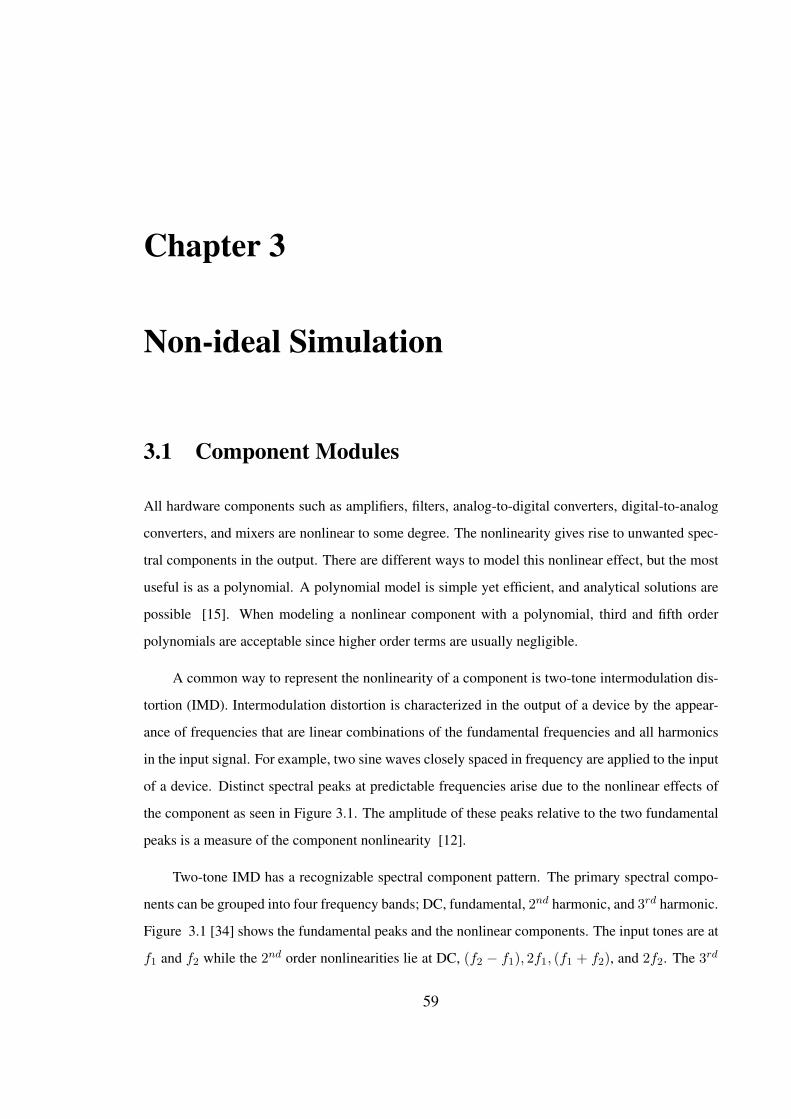
A common way to represent the nonlinearity of a component is two-tone intermodulation dis-
tortion (IMD). Intermodulation distortion is characterized in the output of a device by the appear-
ance of frequencies that are linear combinations of the fundamental frequencies and all harmonics
in the input signal. For example, two sine waves closely spaced in frequency are applied to the input
of a device. Distinct spectral peaks at predictable frequencies arise due to the nonlinear effects of
the component as seen in Figure 3.1. The amplitude of these peaks relative to the two fundamental
peaks is a measure of the component nonlinearity [12].
Two-tone IMD has a recognizable spectral component pattern. The primary spectral compo-
nents can be grouped into four frequency bands; DC, fundamental, 2nd harmonic, and 3rd harmonic.
Figure 3.1 [34] shows the fundamental peaks and the nonlinear components. The input tones are at
f1 and f2 while the 2nd order nonlinearities lie at DC, (f2 − f1), 2f1, (f1 + f2), and 2f2. The 3rd
59

order nonlinearities lie at (2f1−f2), f1, f2, (2f2−f1), 3f1, (2f1 +f2), (f1 +2f2), and 3f2, though
the components at the fundamental frequency are smaller in amplitude than the input tones. The
components in the fundamental band are of interest because they are “in-band”. The components
not “in-band” can usually be filtered out. The “in-band” components are generated by the 3rd order
nonlinearities, and therefore, the odd order polynomial coefficients in the nonlinear model are of
special interest [15].
Figure 3.1: Two-tone Intermodulation Distortion
Another way that nonlinearities in components are defined is by use of intercept points and
compression points. When the power input to a component is increased, the nonlinear spectral
parameters of the component increase faster in amplitude than the fundamentals. The 2nd order
polynomial slope increases at a rate of 2 output dB per input dB while the 3rd order polynomial
slope increases at a rate of 3 output dB per input dB. Therefore there is a point at which the output
power of the nonlinear spectral components is equal to the output power of the fundamentals. That
point is called the intercept point [12]. Figure 3.2 [34] shows this intercept point for the 3rd order
case, specified either by input power as iIP3, or output power as oIP3. The roll off of both the
fundamental as well as the 3rd order nonlinear spectral component is due to compression.
The component can be additionally characterized by the output 1 dB compression point, or
oCP1. Compression is defined as what happens when the actual output power falls below the ideal
output power. The output power could also reach its maximum, which results in saturation. The
nonlinear component will experience compression and eventually saturation as the input power to
the component is increased [21]. The compression point is the output power value that falls 1 dB
below the ideal output power [15, 12, 21]. This is illustrated in figure 3.3 [34].
Most components also contain noise which causes nonlinearities. There are three sources of
noise in a component; flicker, thermal, and shot noise. Flicker, or 1f noise is believed to be caused
60
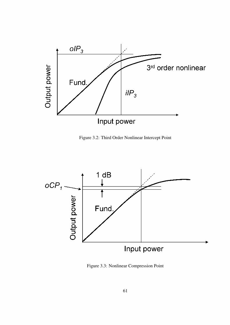
Figure 3.2: Third Order Nonlinear Intercept Point
Figure 3.3: Nonlinear Compression Point
61

by defects and contaminants in semiconductor crystals, though the origin is a subject of current
research. Flicker noise typically occurs at low frequencies or audio band and has a spectrum that
varies inversely with frequency [20].
Thermal noise is generated within the resistors of the component and is proportional to the
temperature of the system. Thermal noise has a spectrum that is white, or flat [16, 20] as does shot
noise. The discrete fluctuations of current through the component results in shot noise. Shot noise
is therefore proportional to the level of current through the device [20]. For most components, one
of the white spectrum noise sources will dominate. As a result, the noise figure can be characterized
by a single noise power level and modeled with a white spectrum.
3.1.1 Frequency Modulation
Oscillator
The main cause of nonlinearity in an oscillator is phase noise. Phase noise is defined as the ratio
of the noise in a 1 Hz bandwidth at a specified frequency offset relative to the oscillator signal
amplitude at the carrier frequency [28]. The phase noise spectrum can be very complicated. The
noise can arise from a number of different sources and it also depends on the type of device. En-
vironmental factors such as vibration, mechanical shock, and temperature can cause noise. The
oscillator module in Matlab uses a known single sideband spectrum, a known root mean squared
(RMS) timing jitter, or a peak-to-peak timing jitter to model the phase noise.
If a single sideband spectrum is known, a white noise Gaussian signal [24] is shaped with the
known spectrum. RMS timing jitter is defined as one standard deviation of the normal phase noise
distribution [5]. If this jitter value is known, a flat white noise spectrum is assumed and scaled to
give the correct RMS jitter. Peak-to-peak timing jitter is defined as the distance from the largest to
the smallest measurement on the normal curve [5]. If the phase noise is specified by the peak-to-
peak timing jitter, that specified value is converted to RMS jitter simply by dividing by 6 which is
a good approximation for a Gaussian distribution. After the conversion from peak-to-peak to RMS,
the RMS jitter approach is used to model the phase noise.
If the single sideband spectrum is known, the oscillator module takes as inputs the phase noise
frequencies and phase noise powers while the RMS and peak-to-peak jitter parameters are left un-
62
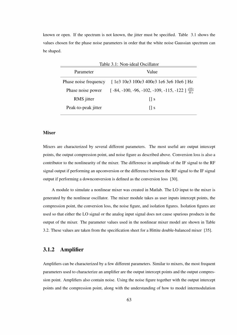
known or open. If the spectrum is not known, the jitter must be specified. Table 3.1 shows the
values chosen for the phase noise parameters in order that the white noise Gaussian spectrum can
be shaped.
Table 3.1: Non-ideal Oscillator
Parameter Value
Phase noise frequency [ 1e3 10e3 100e3 400e3 1e6 3e6 10e6 ] Hz
Phase noise power [ -84, -100, -96, -102, -109, -115, -122 ] dBcHz
RMS jitter [] s
Peak-to-peak jitter [] s
Mixer
Mixers are characterized by several different parameters. The most useful are output intercept
points, the output compression point, and noise figure as described above. Conversion loss is also a
contributor to the nonlinearity of the mixer. The difference in amplitude of the IF signal to the RF
signal output if performing an upconversion or the difference between the RF signal to the IF signal
output if performing a downconversion is defined as the conversion loss [30].
A module to simulate a nonlinear mixer was created in Matlab. The LO input to the mixer is
generated by the nonlinear oscillator. The mixer module takes as user inputs intercept points, the
compression point, the conversion loss, the noise figure, and isolation figures. Isolation figures are
used so that either the LO signal or the analog input signal does not cause spurious products in the
output of the mixer. The parameter values used in the nonlinear mixer model are shown in Table
3.2. These values are taken from the specification sheet for a Hittite double-balanced mixer [35].
3.1.2 Amplifier
Amplifiers can be characterized by a few different parameters. Similar to mixers, the most frequent
parameters used to characterize an amplifier are the output intercept points and the output compres-
sion point. Amplifiers also contain noise. Using the noise figure together with the output intercept
points and the compression point, along with the understanding of how to model intermodulation
63
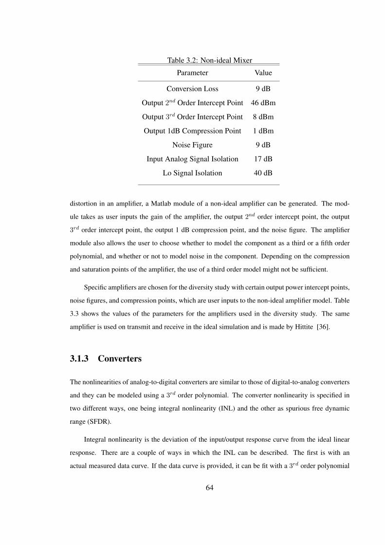
Table 3.2: Non-ideal Mixer
Parameter Value
Conversion Loss 9 dB
Output 2nd Order Intercept Point 46 dBm
Output 3rd Order Intercept Point 8 dBm
Output 1dB Compression Point 1 dBm
Noise Figure 9 dB
Input Analog Signal Isolation 17 dB
Lo Signal Isolation 40 dB
distortion in an amplifier, a Matlab module of a non-ideal amplifier can be generated. The mod-
ule takes as user inputs the gain of the amplifier, the output 2nd order intercept point, the output
3rd order intercept point, the output 1 dB compression point, and the noise figure. The amplifier
module also allows the user to choose whether to model the component as a third or a fifth order
polynomial, and whether or not to model noise in the component. Depending on the compression
and saturation points of the amplifier, the use of a third order model might not be sufficient.
Specific amplifiers are chosen for the diversity study with certain output power intercept points,
noise figures, and compression points, which are user inputs to the non-ideal amplifier model. Table
3.3 shows the values of the parameters for the amplifiers used in the diversity study. The same
amplifier is used on transmit and receive in the ideal simulation and is made by Hittite [36].
3.1.3 Converters
The nonlinearities of analog-to-digital converters are similar to those of digital-to-analog converters
and they can be modeled using a 3rd order polynomial. The converter nonlinearity is specified in
two different ways, one being integral nonlinearity (INL) and the other as spurious free dynamic
range (SFDR).
Integral nonlinearity is the deviation of the input/output response curve from the ideal linear
response. There are a couple of ways in which the INL can be described. The first is with an
actual measured data curve. If the data curve is provided, it can be fit with a 3rd order polynomial
64

Table 3.3: Non-ideal Amplifier
Location Parameter Value
Gain 43 dB
Output 2nd Order Intercept Point 56 dBm
Transmit Output 3rd Order Intercept Point 59 dBm
Output 1dB Compression Point 43 dBm
Noise Figure 8.5 dB
Gain 13 dB
Output 2nd Order Intercept Point 37 dBm
Receive Output 3rd Order Intercept Point 37 dBm
Output 1dB Compression Point 22 dBm
Noise Figure 1.6 dB
curve. The second is by a statistical maximum standard deviation from the ideal. If the curve is not
provided, a third order shape is assumed and scaled to fit the maximum standard deviation.
The dynamic range of the device output which is free of spurious spectral components, either
due to nonlinearities or noise is called the spurious free dynamic range. The SFDR is usually given
in decibels for a particular frequency and input level [13]. The shape is again assumed to be 3rd
order, and scaled to fit the specified SFDR performance.
Digital-to-Analog Converter
The digital-to-analog converter module has many user defined inputs. Among them are the resolu-
tion, output voltage constraints, maximum expected offset error, maximum expected full scale gain
error, and settling time. Offset error indicates how well the actual transfer function matches the
ideal transfer function at a certain point. For DACs that means the analog output response to an
input of all zeros [6]. Full scale gain error is defined as the difference between the actual and ideal
output voltage range [6]. Settling time is defined as the amount of time required for the DAC out-
put to settle, within a specific tolerance, to a certain level [19]. Also as user inputs are the integral
nonlinearity and the noise spectral density. The default inputs are shown in table 3.4, modeling a
65
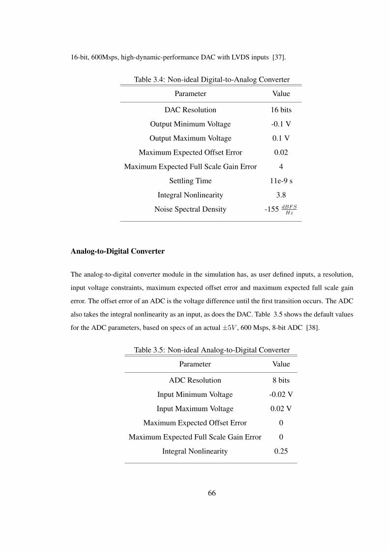
16-bit, 600Msps, high-dynamic-performance DAC with LVDS inputs [37].
Table 3.4: Non-ideal Digital-to-Analog Converter
Parameter Value
DAC Resolution 16 bits
Output Minimum Voltage -0.1 V
Output Maximum Voltage 0.1 V
Maximum Expected Offset Error 0.02
Maximum Expected Full Scale Gain Error 4
Settling Time 11e-9 s
Integral Nonlinearity 3.8
Noise Spectral Density -155 dBFSHz
Analog-to-Digital Converter
The analog-to-digital converter module in the simulation has, as user defined inputs, a resolution,
input voltage constraints, maximum expected offset error and maximum expected full scale gain
error. The offset error of an ADC is the voltage difference until the first transition occurs. The ADC
also takes the integral nonlinearity as an input, as does the DAC. Table 3.5 shows the default values
for the ADC parameters, based on specs of an actual ±5V , 600 Msps, 8-bit ADC [38].
Table 3.5: Non-ideal Analog-to-Digital Converter
Parameter Value
ADC Resolution 8 bits
Input Minimum Voltage -0.02 V
Input Maximum Voltage 0.02 V
Maximum Expected Offset Error 0
Maximum Expected Full Scale Gain Error 0
Integral Nonlinearity 0.25
66

3.1.4 Analog Filter
Analog filters are modeled as infinite impulse response (IIR) filters. The most efficient are of But-
terworth, Chebyshev, or Elliptical design [22]. Analog filters have nonlinear properties as do most
hardware components. The nonlinearities in analog filters are insertion loss, nonlinear response
curves, and noise. Insertion loss is defined as attenuation of the pass band signal due to losses
within the component. Insertion loss is modeled with a random scale factor within component
specification.
Analog filters have a nonlinear response curve that could potentially produce intermodulation.
This type of response curve typically has a small effect on the nonlinearity of the component, and
can therefore be easily controlled with a small input amplitude. However, the nonlinearity con-
tributed by the nonlinear response curve is not normally modeled because the curve parameters are
not typically given in the component specification sheet. Analog filters also contain noise that ef-
fects the nonlinearity of the component. Again, however, the noise is not typically modeled because
the values are not normally given on the specification sheet.
A Matlab module of an analog filter is designed. The module takes in as user inputs the type
of filter, being Butterworth, Chebyshev Type I, Chebyshev Type II, or Elliptical. The pass-band and
stop-band frequencies and attenuations can also be specified by the user. The last user input is the
insertion loss. Table 3.6 shows the default type of filter and the default value of the insertion loss for
each of the analog filters on transmit and receive, both high-pass and low-pass. The pass-band and
stop-band frequencies for the two filters on transmit can be changed to suit the simulation needs.
The pass-band and stop-band frequencies of the filter on receive, however, are based upon the IF
frequencies that were previously specified. Therefore, the edge frequencies of the low-pass filter on
receive can not be changed by the user. It is also important to note that the analog filter module can
not have a transition width of less than 500 MHz.
3.1.5 Time Delay Network
The time delay network block values did not change much between the ideal values and the non-
ideal values. The target properties all remained the same, but the signal amplitude scale value
changed. The ideal simulation used a signal amplitude scale value of one. The signal amplitude
67
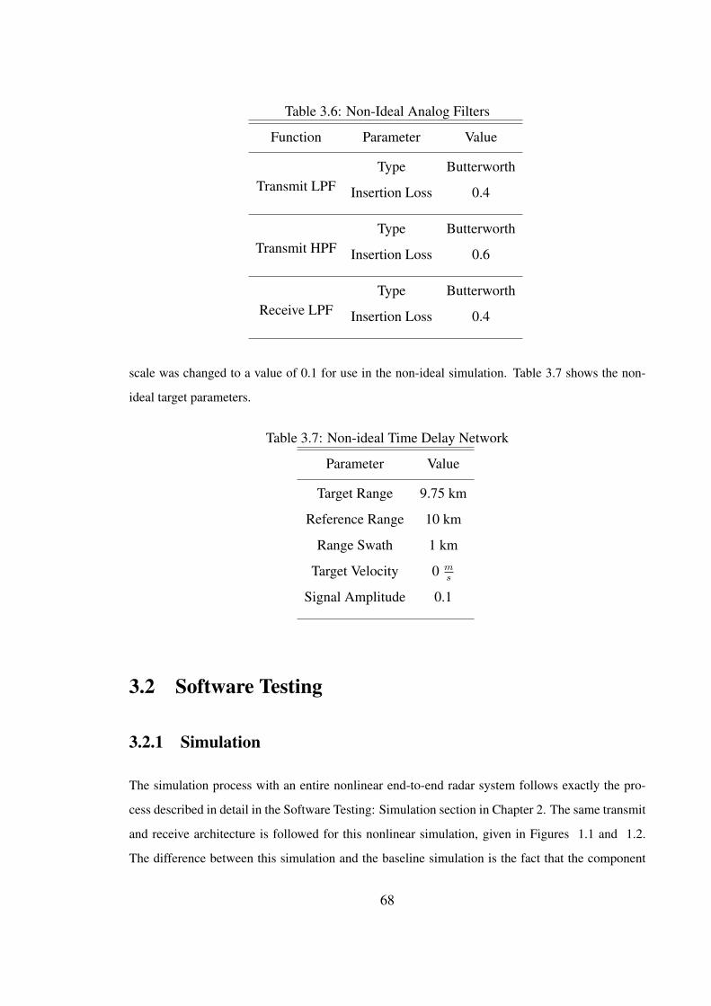
Table 3.6: Non-Ideal Analog Filters
Function Parameter Value
Type ButterworthTransmit LPF Insertion Loss 0.4
Type ButterworthTransmit HPF Insertion Loss 0.6
Type ButterworthReceive LPF Insertion Loss 0.4
scale was changed to a value of 0.1 for use in the non-ideal simulation. Table 3.7 shows the non-
ideal target parameters.
Table 3.7: Non-ideal Time Delay Network
Parameter Value
Target Range 9.75 km
Reference Range 10 km
Range Swath 1 km
Target Velocity 0 ms
Signal Amplitude 0.1
3.2 Software Testing
3.2.1 Simulation
The simulation process with an entire nonlinear end-to-end radar system follows exactly the pro-
cess described in detail in the Software Testing: Simulation section in Chapter 2. The same transmit
and receive architecture is followed for this nonlinear simulation, given in Figures 1.1 and 1.2.
The difference between this simulation and the baseline simulation is the fact that the component
68
models used, the converters, filters, mixers, and amplifiers have added nonlinearities to the mod-
eling. Therefore, some detail and plots may not be in this simulation due to the fact that the ideal
simulation generated the same plot.
For simplicity, this nonlinear simulation uses many of the same parameters as the baseline
simulation pending that the module in question does not include nonlinear affects. The waveform
generation, digital upsample, IF modulation, and digital summation processes are the same as in the
baseline simulation. So to recap, 38 pulses are generated, three frequency channels are used, and the
respective IF frequencies are 200 MHz, 300 MHz, and 400 MHz, respectively. The pulse repetition
frequency and the integration time used to calculate the number of pulses are given in Table 2.1.
Now the signal encounters the first nonlinear component, the digital-to-analog converter. The
DAC output signal is shown in Figure 3.4 along with its corresponding frequency spectrum in Fig-
ure 3.5. It is known that the nonlinearity of the DAC adds unwanted harmonics to the signal. These
harmonics decrease in amplitude as the frequency increases. The harmonics can be seen in the
frequency spectrum of the output signal.
A low pass filter is needed such the harmonics do not affect the DAC output signal. The
nonlinear parameter of the Butterworth low pass filter used is given in Table 3.6. The pass band
edge frequency of the filter is 250 MHz while the stop band edge frequency is 750 MHz. These
edge frequencies meet the transition width requirement of the filter model and they also allow the
correct frequency components to pass through, that is, the components at the IF frequencies. The
low pass filtered output and frequency spectrum are shown in Figures 3.6 and 3.7, respectively.
The signal is now in the analog domain, and the nonlinear mixer module can be used to mod-
ulate the signal up to the RF frequency. The RF frequency is the same as in the ideal simulation
which is 2 GHz. The signal is shown in Figure 3.8 and, by inspection, is noticeably noisier than
the modulated signal in the baseline simulation shown in Figure 2.7. The frequency spectrum of
the signal should show two peaks as explained mathematically by Equation 1.4. The peaks should
appear at fRF and (fRF − 2fIF ), or in this case 2 GHz and 1.4 GHz. The frequency spectrum of
the signal at RF, shown in Figure 3.9 shows this to be true.
The frequency components of the signal which are needed are the components at 2 GHz. There-
fore, a high pass filter is needed. The nonlinear analog filter module is used to filter the signal. The
nonlinear parameters of this high pass filter are given in Table 3.6. The stop band and pass band
69
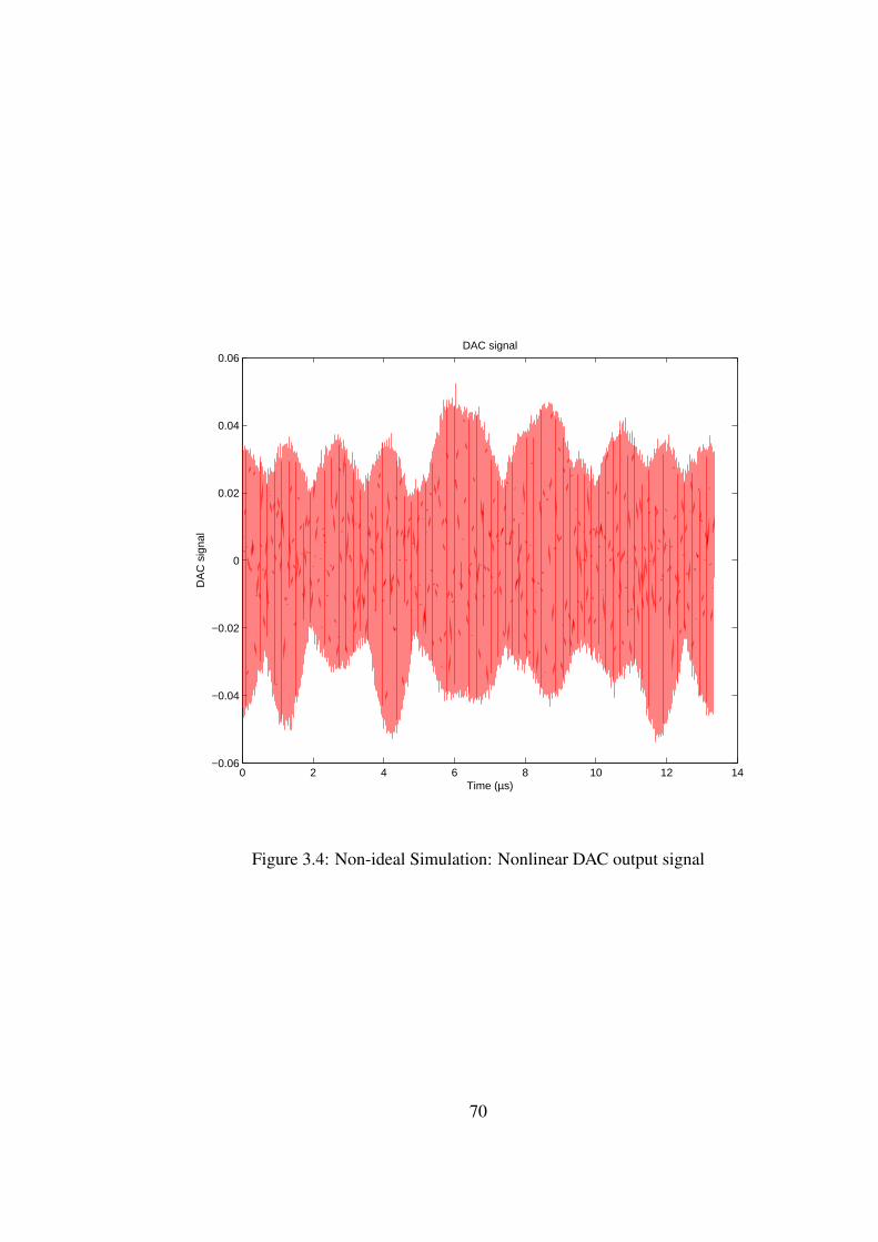
0 2 4 6 8 10 12 14−0.06
−0.04
−0.02
0
0.02
0.04
0.06
DA
C s
igna
l
Time (µs)
DAC signal
Figure 3.4: Non-ideal Simulation: Nonlinear DAC output signal
70

0 5 10 15 20 25−60
−40
−20
0
20
40
60
80
DA
C s
pect
rum
Frequency (GHz)
DAC frequency spectrum
Figure 3.5: Non-ideal Simulation: Nonlinear DAC output signal spectrum
71

0 2 4 6 8 10 12 14−0.04
−0.03
−0.02
−0.01
0
0.01
0.02
0.03
0.04
Filt
ered
Sig
nal
Time (µs)
Analog Filtered Signal
Figure 3.6: Non-ideal Simulation: Low pass filtered signal after filtering out unwanted
DAC harmonics
72
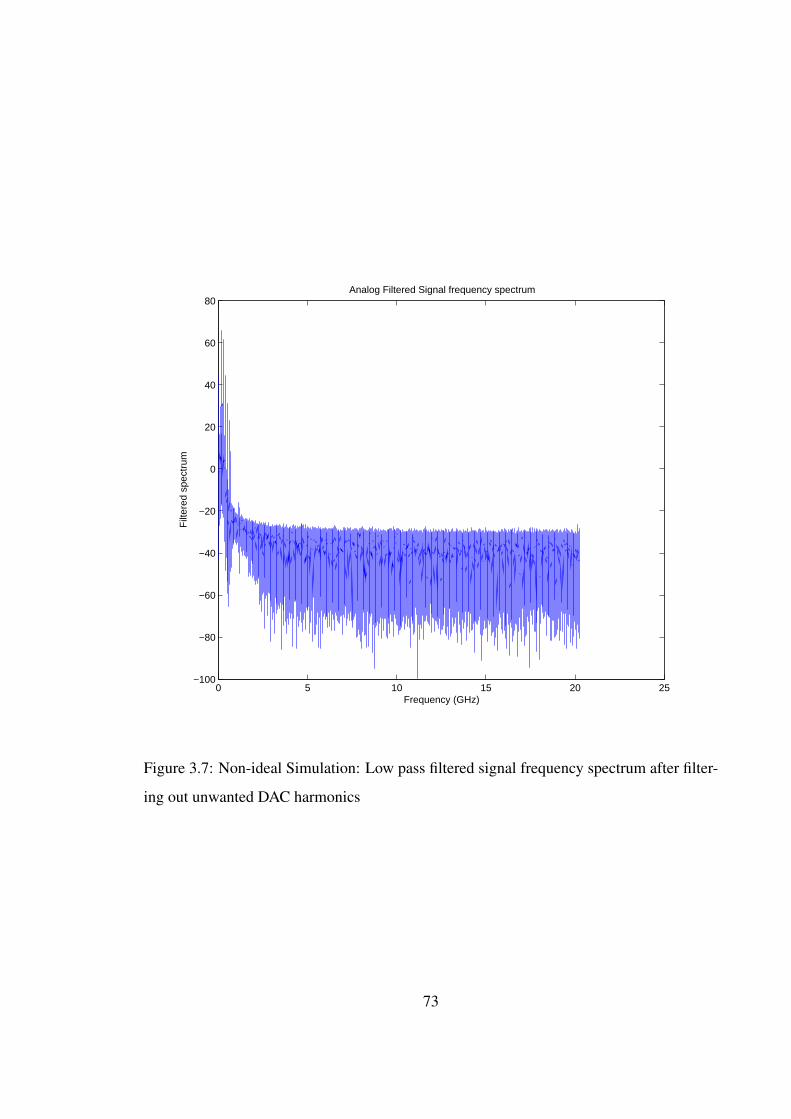
0 5 10 15 20 25−100
−80
−60
−40
−20
0
20
40
60
80
Filt
ered
spe
ctru
m
Frequency (GHz)
Analog Filtered Signal frequency spectrum
Figure 3.7: Non-ideal Simulation: Low pass filtered signal frequency spectrum after filter-
ing out unwanted DAC harmonics
73

0 2 4 6 8 10 12 14−0.06
−0.04
−0.02
0
0.02
0.04
0.06
0.08
0.1
Time (µs)
Analog signal from mixer
Figure 3.8: Non-ideal Simulation: RF mixer output signal
74
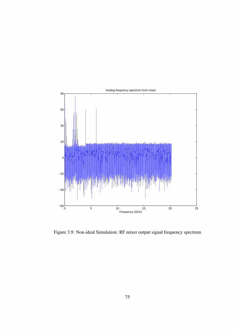
0 5 10 15 20 25−60
−40
−20
0
20
40
60
80Analog frequency spectrum from mixer
Frequency (GHz)
Figure 3.9: Non-ideal Simulation: RF mixer output signal frequency spectrum
75

edge frequencies are 199.5 and 2 GHz, respectively, satisfying the analog filter module transition
width requirement. The signal frequency spectrum now only consists of the high frequency compo-
nents as seen in Figure 3.11.
0 2 4 6 8 10 12 14−0.06
−0.04
−0.02
0
0.02
0.04
0.06
Filt
ered
Sig
nal
Time (µs)
Analog Filtered Signal
Figure 3.10: Non-ideal Simulation: High pass filter output signal following RF mixer
In reference to the system architecture in Figure 1.1, the next step in the transmit chain is an
amplifier. The nonlinear amplifier parameters are given in Table 3.3. This amplifier is modeled
with a third order polynomial. Noise is also included in the amplifier model. After the signal is
amplified, the signal is time delayed. The same time delay network parameters are used for this
nonlinear simulation as were used in the baseline simulation. Those parameters are given in Table
2.3. The same equations are used to calculate the actual target range as well as the time delay. Since
the parameters remain the same, the calculated time delay is 65µs.
After the signal is received, a power amplifier is again needed. The amplifier model used in the
receive chain is the same as the model in the transmit chain. A third order polynomial along with
76
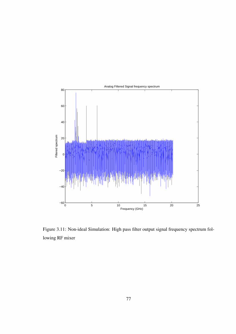
0 5 10 15 20 25−60
−40
−20
0
20
40
60
80
Filt
ered
spe
ctru
m
Frequency (GHz)
Analog Filtered Signal frequency spectrum
Figure 3.11: Non-ideal Simulation: High pass filter output signal frequency spectrum fol-
lowing RF mixer
77

noise are used to model the receive amplifier. The signal, though delayed and amplified is still at RF
frequency. According to the receive architecture, Figure 1.2 , the first demodulation to take place
is from RF to IF frequency. The analog mixer module is used for this demodulation process. The
demodulated signal is shown in Figure 3.12. The frequency spectrum of the demodulated signal
should again show two peaks as seen mathematically in Equation 1.7. This mixing process should
produce peaks at (2fRF − fIF ) and fIF . Since this nonlinear simulation is using three frequency
channels, there should be three peaks at the three high frequencies, 2fRF minus each one of the IF
frequencies, and three peaks at each of the IF frequencies. This is verified in the plot of the signal
spectrum, Figure 3.13.
0 2 4 6 8 10 12 14 16 18 20−0.15
−0.1
−0.05
0
0.05
0.1
0.15
0.2
Time (µs)
Analog signal from mixer
Figure 3.12: Non-ideal Simulation: RF demodulated signal
The required components of the signal are the low frequency components. Therefore, a low
pass filter is needed. The analog filter module is again used with the nonlinear parameter value
given in Table 3.6. Note that the average IF frequency is 300 MHz. Due to the transition width
requirement of the analog filter module, the pass band edge frequency is 200 MHz higher than the
78
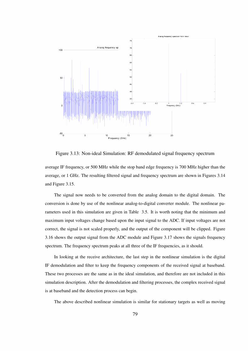
Figure 3.13: Non-ideal Simulation: RF demodulated signal frequency spectrum
average IF frequency, or 500 MHz while the stop band edge frequency is 700 MHz higher than the
average, or 1 GHz. The resulting filtered signal and frequency spectrum are shown in Figures 3.14
and Figure 3.15.
The signal now needs to be converted from the analog domain to the digital domain. The
conversion is done by use of the nonlinear analog-to-digital converter module. The nonlinear pa-
rameters used in this simulation are given in Table 3.5. It is worth noting that the minimum and
maximum input voltages change based upon the input signal to the ADC. If input voltages are not
correct, the signal is not scaled properly, and the output of the component will be clipped. Figure
3.16 shows the output signal from the ADC module and Figure 3.17 shows the signals frequency
spectrum. The frequency spectrum peaks at all three of the IF frequencies, as it should.
In looking at the receive architecture, the last step in the nonlinear simulation is the digital
IF demodulation and filter to keep the frequency components of the received signal at baseband.
These two processes are the same as in the ideal simulation, and therefore are not included in this
simulation description. After the demodulation and filtering processes, the complex received signal
is at baseband and the detection process can begin.
The above described nonlinear simulation is similar for stationary targets as well as moving
79

0 2 4 6 8 10 12 14 16 18 20−0.015
−0.01
−0.005
0
0.005
0.01
0.015
0.02
Filt
ered
Sig
nal
Time (µs)
Analog Filtered Signal
Figure 3.14: Non-ideal Simulation: Low pass filter output signal following RF demodula-
tion
80

0 5 10 15 20 25−120
−100
−80
−60
−40
−20
0
20
40
60
80
Filt
ered
spe
ctru
m
Frequency (GHz)
Analog Filtered Signal frequency spectrum
Figure 3.15: Non-ideal Simulation: Low pass filter output signal frequency spectrum fol-
lowing RF demodulation
81

0 2 4 6 8 10 12 14 16 18 20−60
−40
−20
0
20
40
60
80
100
120
AD
C s
igna
l
Time (µs)
ADC signal
Figure 3.16: Non-ideal Simulation: Nonlinear ADC output signal
82

0 50 100 150 200 250 300 350 400 4500
20
40
60
80
100
120
AD
C s
pect
rum
Frequency (MHz)
ADC frequency spectrum
Figure 3.17: Non-ideal Simulation: Nonlinear ADC output signal frequency spectrum
83
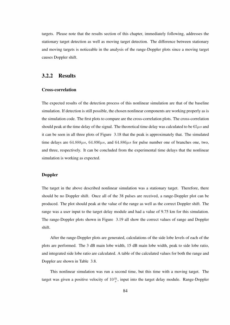
targets. Please note that the results section of this chapter, immediately following, addresses the
stationary target detection as well as moving target detection. The difference between stationary
and moving targets is noticeable in the analysis of the range-Doppler plots since a moving target
causes Doppler shift.
3.2.2 Results
Cross-correlation
The expected results of the detection process of this nonlinear simulation are that of the baseline
simulation. If detection is still possible, the chosen nonlinear components are working properly as is
the simulation code. The first plots to compare are the cross-correlation plots. The cross-correlation
should peak at the time delay of the signal. The theoretical time delay was calculated to be 65µs and
it can be seen in all three plots of Figure 3.18 that the peak is approximately that. The simulated
time delays are 64.888µs, 64.890µs, and 64.886µs for pulse number one of branches one, two,
and three, respectively. It can be concluded from the experimental time delays that the nonlinear
simulation is working as expected.
Doppler
The target in the above described nonlinear simulation was a stationary target. Therefore, there
should be no Doppler shift. Once all of the 38 pulses are received, a range-Doppler plot can be
produced. The plot should peak at the value of the range as well as the correct Doppler shift. The
range was a user input to the target delay module and had a value of 9.75 km for this simulation.
The range-Doppler plots shown in Figure 3.19 all show the correct values of range and Doppler
shift.
After the range-Doppler plots are generated, calculations of the side lobe levels of each of the
plots are performed. The 3 dB main lobe width, 15 dB main lobe width, peak to side lobe ratio,
and integrated side lobe ratio are calculated. A table of the calculated values for both the range and
Doppler are shown in Table 3.8.
This nonlinear simulation was run a second time, but this time with a moving target. The
target was given a positive velocity of 10ms , input into the target delay module. Range-Doppler
84
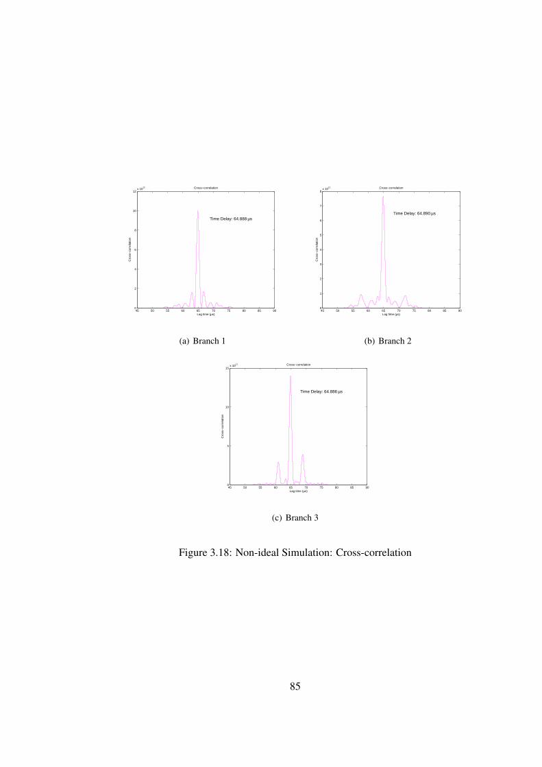
45 50 55 60 65 70 75 80 85 900
2
4
6
8
10
12x 10
12
Lag time (µs)
Cro
ss−
corr
elat
ion
Cross−correlation
Time Delay: 64.888 µs
(a) Branch 1
45 50 55 60 65 70 75 80 85 900
1
2
3
4
5
6
7
8x 10
12
Lag time (µs)C
ross
−co
rrel
atio
n
Cross−correlation
Time Delay: 64.890 µs
(b) Branch 2
45 50 55 60 65 70 75 80 85 900
5
10
15x 10
11
Lag time (µs)
Cro
ss−
corr
elat
ion
Cross−correlation
Time Delay: 64.886 µs
(c) Branch 3
Figure 3.18: Non-ideal Simulation: Cross-correlation
85
Doppler Shift: Branch 1
Fre
quen
cy s
hift
(Hz)
Range (km)9.3 9.4 9.5 9.6 9.7 9.8 9.9 10 10.1 10.2
−250
−200
−150
−100
−50
0
50
100
150
200
250
(a) Branch 1
Doppler Shift: Branch 2
Fre
quen
cy s
hift
(Hz)
Range (km)9.3 9.4 9.5 9.6 9.7 9.8 9.9 10 10.1 10.2
−250
−200
−150
−100
−50
0
50
100
150
200
250
(b) Branch 2
Doppler Shift: Branch 3
Fre
quen
cy s
hift
(Hz)
Range (km)9.3 9.4 9.5 9.6 9.7 9.8 9.9 10 10.1 10.2
−250
−200
−150
−100
−50
0
50
100
150
200
250
(c) Branch 3
Figure 3.19: Non-ideal Simulation: Range-Doppler plots for zero Doppler shift
86
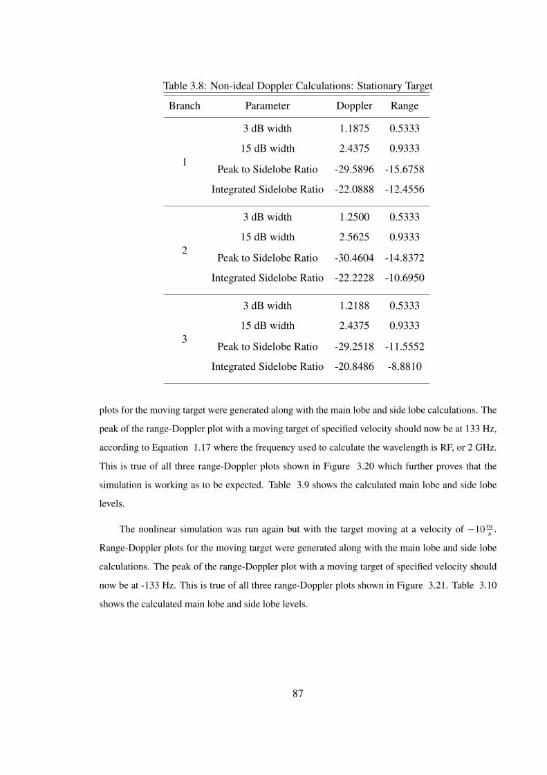
Table 3.8: Non-ideal Doppler Calculations: Stationary Target
Branch Parameter Doppler Range
3 dB width 1.1875 0.5333
15 dB width 2.4375 0.93331
Peak to Sidelobe Ratio -29.5896 -15.6758
Integrated Sidelobe Ratio -22.0888 -12.4556
3 dB width 1.2500 0.5333
15 dB width 2.5625 0.93332
Peak to Sidelobe Ratio -30.4604 -14.8372
Integrated Sidelobe Ratio -22.2228 -10.6950
3 dB width 1.2188 0.5333
15 dB width 2.4375 0.93333
Peak to Sidelobe Ratio -29.2518 -11.5552
Integrated Sidelobe Ratio -20.8486 -8.8810
plots for the moving target were generated along with the main lobe and side lobe calculations. The
peak of the range-Doppler plot with a moving target of specified velocity should now be at 133 Hz,
according to Equation 1.17 where the frequency used to calculate the wavelength is RF, or 2 GHz.
This is true of all three range-Doppler plots shown in Figure 3.20 which further proves that the
simulation is working as to be expected. Table 3.9 shows the calculated main lobe and side lobe
levels.
The nonlinear simulation was run again but with the target moving at a velocity of −10ms .
Range-Doppler plots for the moving target were generated along with the main lobe and side lobe
calculations. The peak of the range-Doppler plot with a moving target of specified velocity should
now be at -133 Hz. This is true of all three range-Doppler plots shown in Figure 3.21. Table 3.10
shows the calculated main lobe and side lobe levels.
87
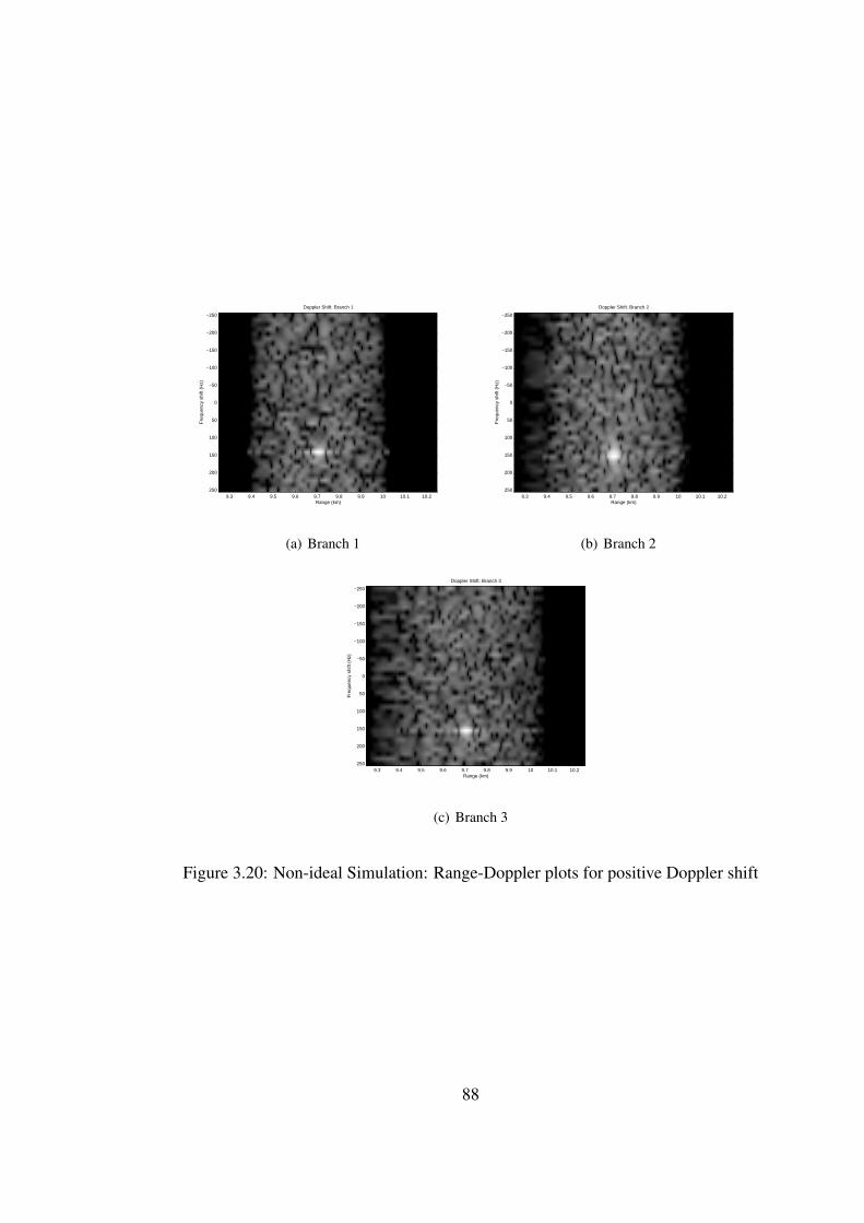
Doppler Shift: Branch 1
Fre
quen
cy s
hift
(Hz)
Range (km)9.3 9.4 9.5 9.6 9.7 9.8 9.9 10 10.1 10.2
−250
−200
−150
−100
−50
0
50
100
150
200
250
(a) Branch 1
Doppler Shift: Branch 2
Fre
quen
cy s
hift
(Hz)
Range (km)9.3 9.4 9.5 9.6 9.7 9.8 9.9 10 10.1 10.2
−250
−200
−150
−100
−50
0
50
100
150
200
250
(b) Branch 2
Doppler Shift: Branch 3
Fre
quen
cy s
hift
(Hz)
Range (km)9.3 9.4 9.5 9.6 9.7 9.8 9.9 10 10.1 10.2
−250
−200
−150
−100
−50
0
50
100
150
200
250
(c) Branch 3
Figure 3.20: Non-ideal Simulation: Range-Doppler plots for positive Doppler shift
88
Doppler Shift: Branch 1
Fre
quen
cy s
hift
(Hz)
Range (km)9.3 9.4 9.5 9.6 9.7 9.8 9.9 10 10.1 10.2
−250
−200
−150
−100
−50
0
50
100
150
200
250
(a) Branch 1
Doppler Shift: Branch 2
Fre
quen
cy s
hift
(Hz)
Range (km)9.3 9.4 9.5 9.6 9.7 9.8 9.9 10 10.1 10.2
−250
−200
−150
−100
−50
0
50
100
150
200
250
(b) Branch 2
Doppler Shift: Branch 3
Fre
quen
cy s
hift
(Hz)
Range (km)9.3 9.4 9.5 9.6 9.7 9.8 9.9 10 10.1 10.2
−250
−200
−150
−100
−50
0
50
100
150
200
250
(c) Branch 3
Figure 3.21: Non-ideal Simulation: Range-Doppler plots for negative Doppler shift
89

Table 3.9: Non-ideal Doppler calculations: Positive Velocity Target
Branch Parameter Doppler Range
3 dB width 1.2188 0.5333
15 dB width 2.4063 0.93331
Peak to Sidelobe Ratio -19.5184 -15.5866
Integrated Sidelobe Ratio -15.2741 -12.3392
3 dB width 1.2500 0.5333
15 dB width 2.5625 0.93332
Peak to Sidelobe Ratio -26.9544 -14.0454
Integrated Sidelobe Ratio -19.6786 -10.4284
3 dB width 1.2188 0.5333
15 dB width 2.500 0.93333
Peak to Sidelobe Ratio -19.8586 -13.4313
Integrated Sidelobe Ratio -16.1785 -9.6804
90
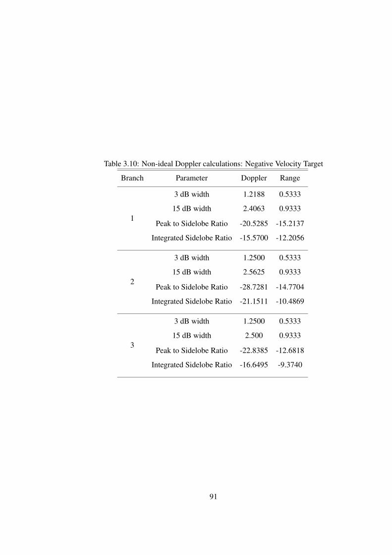
Table 3.10: Non-ideal Doppler calculations: Negative Velocity Target
Branch Parameter Doppler Range
3 dB width 1.2188 0.5333
15 dB width 2.4063 0.93331
Peak to Sidelobe Ratio -20.5285 -15.2137
Integrated Sidelobe Ratio -15.5700 -12.2056
3 dB width 1.2500 0.5333
15 dB width 2.5625 0.93332
Peak to Sidelobe Ratio -28.7281 -14.7704
Integrated Sidelobe Ratio -21.1511 -10.4869
3 dB width 1.2500 0.5333
15 dB width 2.500 0.93333
Peak to Sidelobe Ratio -22.8385 -12.6818
Integrated Sidelobe Ratio -16.6495 -9.3740
91

Chapter 4
Component Parameter Study
The Matlab GUI is designed such that every nonlinear parameter for each component can be mod-
ified. The GUI is especially useful in determining upper and lower bounds on those nonlinear
parameters. Each nonlinear component has certain limitations associated with it. In the following
sections, several parameters to each nonlinear component are changed, one at a time. The entire
end-to-end simulation is then run. An analysis of the range-Doppler side lobe calculations are
performed, along with component saturation and compression limitations. Please note that all of
the simulations run in this study are using three frequency branches of 200, 300, and 400 MHz, a
stationary target, and for the side lobe calculations, the average over the three branches was used.
4.1 Digital-to-Analog Converter
Four nonlinear parameters of the digital-to-analog converter were tested. The first three parameters
tested were the offset error, the full scale gain error, and the integral nonlinearity, none of which
produced any unwanted effects in the range-Doppler side lobe calculations. The offset error ranged
in value from 0.02 to 1 while the corresponding peak to side lobe ratio (PSLR) and integrated side
lobe ratio (ISLR) averaged a change of only 0.2328 and 0.105 dB, respectively. The full scale gain
error ranged from 0.1 to 25, with average changes in PSLR and ISLR being 0.3102 and 0.3150
dB, respectively. The integral nonlinearity values ranged from 1 to 30, only changing the PSLR
by 1.1792 dB and the ISLR by 0.3507 dB, on average. The changes in these three nonlinear DAC
parameters also did not effect the cross-correlation of the signal in any way.
92
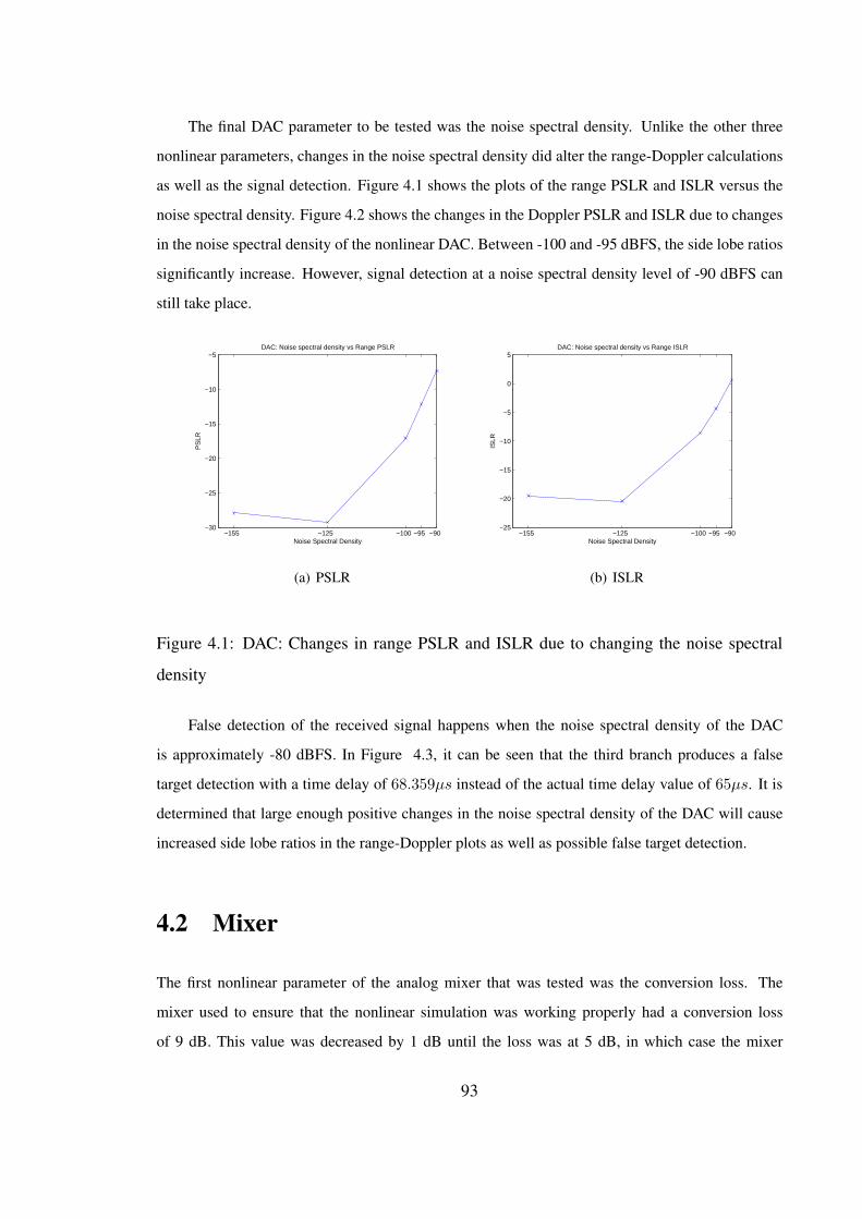
The final DAC parameter to be tested was the noise spectral density. Unlike the other three
nonlinear parameters, changes in the noise spectral density did alter the range-Doppler calculations
as well as the signal detection. Figure 4.1 shows the plots of the range PSLR and ISLR versus the
noise spectral density. Figure 4.2 shows the changes in the Doppler PSLR and ISLR due to changes
in the noise spectral density of the nonlinear DAC. Between -100 and -95 dBFS, the side lobe ratios
significantly increase. However, signal detection at a noise spectral density level of -90 dBFS can
still take place.
−155 −125 −100 −95 −90−30
−25
−20
−15
−10
−5DAC: Noise spectral density vs Range PSLR
PS
LR
Noise Spectral Density
(a) PSLR
−155 −125 −100 −95 −90−25
−20
−15
−10
−5
0
5DAC: Noise spectral density vs Range ISLR
ISLR
Noise Spectral Density
(b) ISLR
Figure 4.1: DAC: Changes in range PSLR and ISLR due to changing the noise spectral
density
False detection of the received signal happens when the noise spectral density of the DAC
is approximately -80 dBFS. In Figure 4.3, it can be seen that the third branch produces a false
target detection with a time delay of 68.359µs instead of the actual time delay value of 65µs. It is
determined that large enough positive changes in the noise spectral density of the DAC will cause
increased side lobe ratios in the range-Doppler plots as well as possible false target detection.
4.2 Mixer
The first nonlinear parameter of the analog mixer that was tested was the conversion loss. The
mixer used to ensure that the nonlinear simulation was working properly had a conversion loss
of 9 dB. This value was decreased by 1 dB until the loss was at 5 dB, in which case the mixer
93

−155 −125 −100 −95 −90−15
−14
−13
−12
−11
−10
−9
−8
−7
−6DAC: Noise spectral density vs Doppler PSLR
PS
LR
Noise Spectral Density
(a) PSLR
−155 −125 −100 −95 −90−12
−11
−10
−9
−8
−7
−6
−5
−4DAC: Noise spectral density vs Doppler ISLR
ISLR
Noise Spectral Density
(b) ISLR
Figure 4.2: DAC: Changes in Doppler PSLR and ISLR due to changing the noise spectral
density
was in compression on receive with an input compression point of 6 dB. The conversion loss was
then increased from the initial starting value in increments of approximately 5 dB. Around 20 dB,
the range side lobe calculations noticeably changed while the Doppler did not change much at all.
Figure 4.4 shows both the range PSLR and the range ISLR plots. The PSLR ranges in value from
-30 dB to approximately -24 dB, at conversion losses of 6 and 25 dB, respectively. The ISLR ranges
from -22 dB to -16 dB over the same range of conversion loss.
Though the range side lobe calculations significantly changed, it can be seen in Figure 4.5 that
the Doppler side lobe calculations did not. The PSLR and ISLR do appear to increase with the
increased value in mixer conversion loss, however the increase is on the order of only 1dB.
As the conversion loss was increased, the mixer did not saturate or compress though the range-
Doppler side lobe levels changed. However, problems did arise in the cross-correlation detection.
Figure 4.6 shows the cross correlation plots for all three branches with a mixer conversion loss of
30 dB. The side lobes are clearly larger than the side lobe levels in the baseline and nonlinear simu-
lations discussed in the previous chapters. To further investigate the overall effect of the increase in
conversion loss on the side lobe levels of the cross-correlation, the parameter was increased again
to 40 dB. Figure 4.7 shows the resulting cross-correlations. The cross-correlation plot of branch 2
produces a false target detection. The side lobe levels are greater than that of the main lobe causing
a false target detection. Therefore, a conversion loss value of less than 6 dB causes compression
94

45 50 55 60 65 70 75 80 85 900
2
4
6
8
10
12x 10
10
Lag time (µs)
Cro
ss−
corr
elat
ion
Cross−correlation
Time Delay: 64.777 µs
(a) Branch 1
45 50 55 60 65 70 75 80 85 900
0.5
1
1.5
2
2.5
3
3.5
4
4.5x 10
10
Lag time (µs)
Cro
ss−
corr
elat
ion
Cross−correlation
Time Delay: 64.894 µs
(b) Branch 2
45 50 55 60 65 70 75 80 85 900
0.5
1
1.5
2
2.5
3
3.5x 10
10
Lag time (µs)
Cro
ss−
corr
elat
ion
Cross−correlation
Time Delay: 68.359 µs
(c) Branch 3
Figure 4.3: Cross-correlation plots with the DAC noise spectral density = -80 dB
6 7 8 9 15 20 25−31
−30
−29
−28
−27
−26
−25
−24
−23Mixer: Conversion loss vs Range PSLR
PS
LR
Conversion Loss (dB)
(a) PSLR
6 7 8 9 15 20 25−23
−22
−21
−20
−19
−18
−17
−16
−15Mixer: Conversion loss vs Range ISLR
ISLR
Conversion Loss (dB)
(b) ISLR
Figure 4.4: Mixer: Changes in range PSLR and ISLR due to changing the conversion loss
95

6 9 15 20 25−14.6
−14.5
−14.4
−14.3
−14.2
−14.1
−14
−13.9
−13.8
−13.7Mixer: Conversion loss vs Doppler PSLR
PS
LR
Conversion Loss (dB)
(a) PSLR
6 9 15 20 25−11.05
−11
−10.95
−10.9
−10.85
−10.8
−10.75
−10.7
−10.65
−10.6
−10.55Mixer: Conversion loss vs Doppler ISLR
ISLR
Conversion Loss (dB)
(b) ISLR
Figure 4.5: Mixer: Changes in Doppler PSLR and ISLR due to changing the conversion
loss
within the mixer, while a conversion loss of greater than approximately 30 dB will cause false target
detection in the signal cross-correlation.
The second parameter of the mixer that was tested was the noise figure. The noise figure did not
seem to have very much effect on the range-Doppler side lobe calculations nor the cross-correlation.
The simulation was run for noise figures ranging from 0 to 40 dB. The PSLR values fell anywhere
between -30.0737 and -29.6552 dB while the ISLR values fell between -22.3816 and -21.5939 dB,
both ratios having a range of values less than 1 dB. Other nonlinear mixer parameters that could
be tested in the future include both the output 2nd and 3rd order intercept points and the output
compression point as well as the isolation values of the analog in and the LO in signal.
4.3 Amplifier
Three nonlinear parameters were tested in the non-ideal amplifier. The three parameters tested were
the amplifier gain, output compression point, and the noise figure. Since both the non-ideal amplifier
on transmit and receive use the same nonlinear Matlab model, only the transmit amplifier was tested.
The amplifier on receive could be tested in the same way, if needed. It is found that none of the three
parameters had any effect on either the cross-correlation or the range-Doppler metrics. Though as
the gain to the amplifier model was increased, the amplifier approached saturation. Detection was
96

45 50 55 60 65 70 75 80 85 900
0.5
1
1.5
2
2.5
3
3.5x 10
11
Lag time (µs)
Cro
ss−
corr
elat
ion
Cross−correlation
Time Delay: 64.842 µs
(a) Branch 1
45 50 55 60 65 70 75 80 85 900
2
4
6
8
10
12
14
16x 10
10
Lag time (µs)C
ross
−co
rrel
atio
n
Cross−correlation
Time Delay: 65.020 µs
(b) Branch 2
45 50 55 60 65 70 75 80 85 900
1
2
3
4
5
6x 10
10
Lag time (µs)
Cro
ss−
corr
elat
ion
Cross−correlation
Time Delay: 64.963 µs
(c) Branch 3
Figure 4.6: Cross-correlation plots with the mixer conversion loss = 30 dB
97
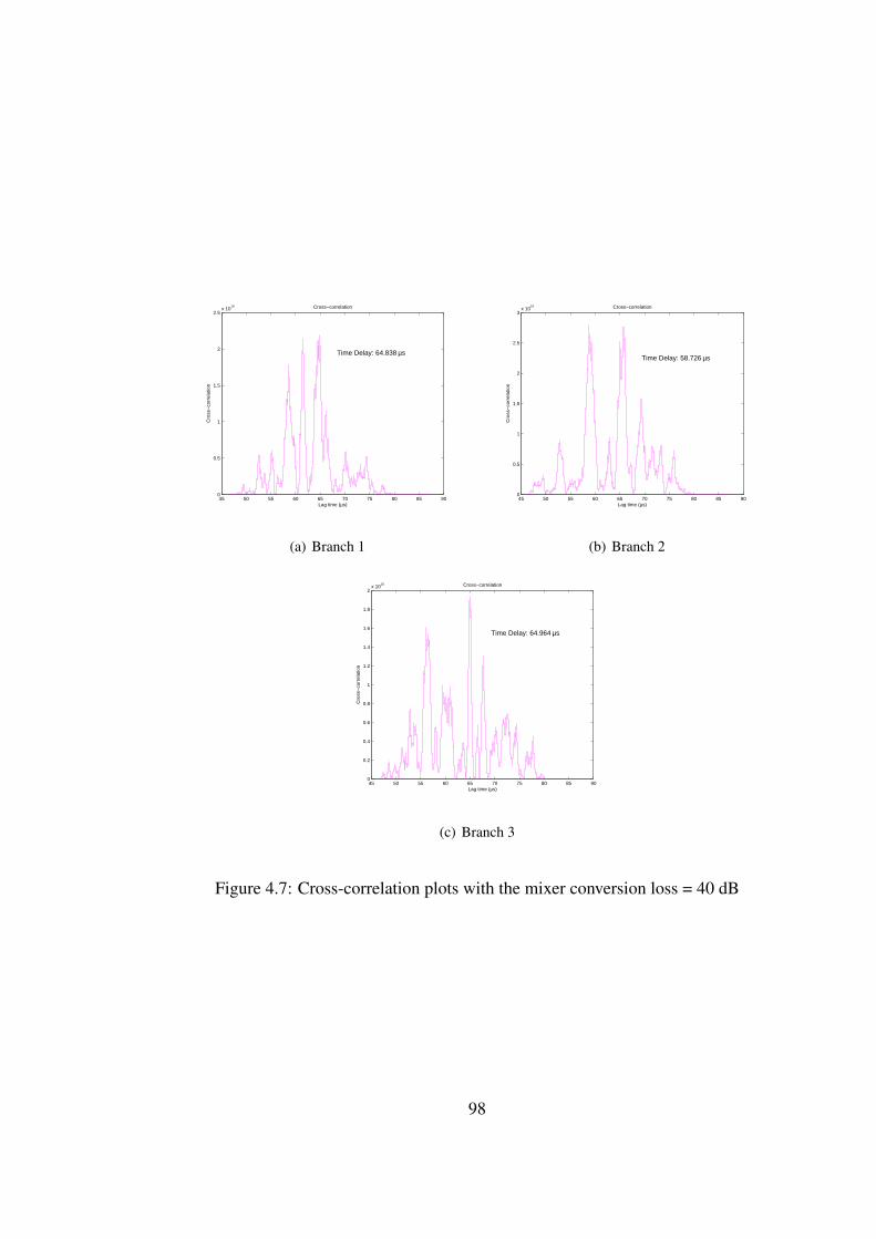
45 50 55 60 65 70 75 80 85 900
0.5
1
1.5
2
2.5x 10
10
Lag time (µs)
Cro
ss−
corr
elat
ion
Cross−correlation
Time Delay: 64.838 µs
(a) Branch 1
45 50 55 60 65 70 75 80 85 900
0.5
1
1.5
2
2.5
3x 10
10
Lag time (µs)C
ross
−co
rrel
atio
n
Cross−correlation
Time Delay: 58.726 µs
(b) Branch 2
45 50 55 60 65 70 75 80 85 900
0.2
0.4
0.6
0.8
1
1.2
1.4
1.6
1.8
2x 10
10
Lag time (µs)
Cro
ss−
corr
elat
ion
Cross−correlation
Time Delay: 64.964 µs
(c) Branch 3
Figure 4.7: Cross-correlation plots with the mixer conversion loss = 40 dB
98
still possible, however, and the side lobe calculations only differed by 1dB for gains from 0dB to
60dB when saturation occurred. The output compression point simply showed the point at which the
non-ideal amplifier was in compression, with no noticeable changes in the PSLR and ISLR values
of the range-Doppler plots. As seen in the mixer also, the noise figure did not seem to have any
effect on either the cross-correlation or the side lobe calculations.
4.4 Analog-to-Digital Converter
Finally, the nonlinear parameters of the analog-to-digital converter were tested. The parameters are
the offset error, the full scale gain error, and the integral nonlinearity; three of the same parameters
as in the nonlinear DAC. The ADC, however, does not have a nonlinear noise spectral density
parameter as the DAC did. Since the functionality of ADCs and DACs is very similar, a theory that
the three aforementioned parameters will not affect the range-Doppler side lobe calculations or the
cross-correlation plots is proposed. After running the simulation with several different values of
each of the three parameters, the proposed theory is validated. Neither the offset error, the full scale
gain error, nor the integral nonlinearity of the ADC affect either the side lobe calculations or the
signal detection. The PSLR and ISLR range of values for all three nonlinear parameters is less than
1 dB.
Please note, though, that in order for the output of the ADC to not get clipped, the correct
minimum and maximum input voltages need to be put into the ADC module. These maximum and
minimum values are found by initially running the simulation and plotting the output of the mixer
low pass filter on receive, the signal that enters the ADC. Observe the amplitude of the low pass
filter output. Those positive and negative amplitudes are now the correct maximum and minimum
input voltage parameters.
99
Chapter 5
Conclusion
5.1 Matlab Software Development
A user friendly graphical interface in Matlab was successfully developed that simulates both the
transmit and receive signal flow of a radar system. The interface allows multiple transmit frequency
channels and the ability to control the waveform for each channel. The interface also allows the user
the capability to control the timing of the waveform as well as the pulse frequency. An important
aspect of the Matlab GUI is the fact that hardware components can easily be interchanged. The
interface also allows for the use of either an ideal or non-ideal component. If a non-ideal component
is chosen, the parameters of the component which contribute to its nonlinearities can be altered
according to the hardware specifications.
An end-to-end baseline radar system was simulated using only ideal, or linear components.
The goal of the baseline simulation was to ensure that ideal hardware components would adequately
detect a time delayed signal as well as produce ambiguity plots with small peak to side lobe and
integrated side lobe ratios. Using the interface described above, an end-to-end baseline simulation
was successfully implemented. The ideal simulation did have the ability to accurately detect a
time delayed signal using cross-correlation. The simulation also produced range-Doppler plots with
sufficient side lobe ratios.
After the baseline simulation was complete, an entire nonlinear system simulation was im-
plemented. The nonlinear simulation used only nonlinear hardware component models. A similar
100
goal was required of the non-ideal simulation. Again, using the Matlab GUI and hardware compo-
nent modules with the ability to change the nonlinearities of each component, an end-to-end radar
system was simulated. The initial goal of the nonlinear simulation was met in that a time delayed
signal was accurately detected, and acceptable peak to side lobe and integrated side lobe ratios of
the range-Doppler plots were produced.
5.2 Nonlinear Parameter Study
Once the baseline as well as the nonlinear simulations were working properly, the usefulness of the
interface was tested. The interface allows for interchanging of nonlinear hardware components such
that the detection properties of each individual component can be tested. Nonlinear parameters of
the DAC, analog mixer, ADC, and amplifier were changed, and the detection process and range-
Doppler ambiguity of each was analyzed.
It was found that the only nonlinear parameter tested that affected the performance of the
digital-to-analog converter was the noise spectral density. As the noise spectral density was changed,
the side lobe calculations for both range and Doppler changed significantly and there was false target
detection. The mixer was tested next and the only nonlinear parameter that caused any performance
changes was the conversion loss. Changing the conversion loss caused false target detection and the
range side lobe calculations changed significantly while the Doppler did not. Finally, the analog-to-
digital converter and amplifier were tested. Since the ADC does not have a noise spectral density
parameter, none of the nonlinear parameters tested contributed to any degradation in performance
of the component. The same was true of the amplifier. The three nonlinear amplifier parameters
tested did not affect the detection or the side lobe calculations of the range-Doppler plots.
5.3 Future Work
As described in the beginning of this document, the waveforms used in the performance study were
binary phase-coded waveforms. In order to further study the impact of current hardware in the fu-
ture, other waveforms of interest can be implemented and studied. Such waveforms include Barker
codes and complementary codes. In using such waveforms as complementary codes, further dif-
ferences between the non-ideal and the ideal simulation should be apparent. Since complementary
101

codes are intended to suppress side lobe levels to very small values, the noise contributions due to
the nonlinearities in the component models should be more noticeable.
102

Bibliography
[1] Hawley, R. and B Rigling, “Waveform Techniques Performance Model for Current GenerationHardware”, ATK Mission Research and Wright State University, 2005
[2] Skolnik, M.I., Introduction to Radar Systems: 3rd Edition, McGraw-Hill, New York, 2001
[3] Skolnik, M.I., Radar Handbook: 2nd Edition, McGraw-Hill, New York, 1990
[4] Lipscomb, J., “SAR Image Quality”, University of Alaska Fairbanks, April 2005,http://www.asf.alaska.edu/educational/seminarpdf/2002/sar image quality.pdf
[5] Roberts, N., “Phase Noise and Jitter - A Primer for Digital Designers”, EE Design, July 2003
[6] “ADC and DAC Glossary”, Maxim/Dallas Semiconductors, Application Note 641, December2000
[7] Hannen, P. and J.C. Toomay, Radar Principles for the Non-Specialist: 3rd Edition, ScitechPublishing, Inc., Raleigh, NC, 2004
[8] http://www.wikipedia.org/wiki/Beamforming, July 2006
[9] Moran, B., S. Suvorova, E. Kalashyan, P. Zulch and R.J. Hancock, “Radar Performance ofTemporal and Frequency Diverse Phase-Coded Waveforms”, 2006
[10] “Waveform Diversity for Multi-Mode Radar”, C & P Technologies, Inc., 2005,http://www.cptnj.com/index.htm
[11] Wicks, M.C. and B. Himed, “Four Problems in Radar”, http://www.nato-us.org/algebra2003/papers/wicks.pdf
[12] Kundert, K., “Accurate and Rapid Measurement of IP2 and IP3”, Designer’s Guide Consult-ing, Inc., May 2002, http://www.designers-guide.org
[13] Pan, H. and A.A. Abidi, “Spectral Spurs Due to Quantization in Nyquist ADCs”, IEEE Trans-actions on Circuits and Systems - I: Regular Papers, 51(8):1422-1439, August 2004
[14] “How Quantization and Thermal Noise Determine an ADC’s Effective Noise Figure”,Maxim/Dallas Semiconductors, September 2002, http://www.maxim-ic.com
[15] Grob, S., “Polynomial Model Derivation of Nonlinear Amplifiers”, Mobile eConference, Au-gust 2004, http://telecom.ece.ntua.gr/eConference/
103
[16] Stensby, J., “Thermal Noise and System Noise Figure”, EE 603 Class notes: Chapter 10, 2004,http://www.ece.uah.edu/courses/ee420-500/
[17] Ellingson, S.W., “A Simple Technique for Measuring Noise Figure”, September 2002,http://telecom.ece.ntua.gr/eConference/
[18] Kester, W., “ADC Noise Figure - An Often Misunderstood and Misinterpreted Specification”,April 2006, http://www.analog.com
[19] Kester, W., “Evaluating High Speed DAC Performance”, January 2006,http://www.analog.com
[20] “Fundamentals of RF and Microwave Noise Figure Measurements”, Application Note 57-1,Agilent Technologies, http://www.agilent.com
[21] Chen, J., “Modeling RF Systems”, Designer’s Guide Consulting, Inc., 2004,http://www.designers-guide.org
[22] Smith, S., The Scientist and Engineer’s Guide to Digital Signal Processing, California Tech-nical Publishing, 1997
[23] Gary, D., “Front End Receiving System”, Radio Astronomy: Lecture 5,http://web.njit.edu/ dgary/
[24] Demir, A., A. Mehrotra, and J. Roychowdhury, “Phase Noise in Oscillators: A Unifying The-ory and Numerical Methods for Characterization”, IEEE Transactions on Circuits and Systems- I: Fundamental Theory and Applications, 47(5):655-674, May 2006
[25] “Characterizing Phase Noise”, Mini-Circuits Inc., January 2003, http://www.rfdesign.com
[26] Drucker, E., “Model PLL Dynamics and Phase Noise Performance”, Microwaves & RF, pages73-82 and 117, February 2000
[27] Grebenkemper, C.J., “Local Oscillator Phase Noise and its Effect on Receiver Performance”,Tech-Notes, November/December 1981
[28] Kester, W., “Converting Oscillator Phase Noise to Time Jitter”, October 2005,http://www.analog.com
[29] Ellis, M., “Introduction to Mixers”, Online Tutorials, 1999,http://members.tripod.com/michaelgellis/tutorial.html
[30] “Mixers”, Microwave Encyclopedia, April 2006, http://www.Microwaves101.com
[31] Vuolevi, J., “Analysis, Measurement and Cancellation of the Bandwidth andAmplitude Dependence of Intermodulation Distortion in RF Power Amplifiers”,University of Oulu: Department of Electrical Engineering, Findland, 2000,http://herkules.oulu.fi/isbn9514265149/html/index.html
[32] “Analog Electronic Filter Design Guide”, Frequency Devices, Inc., August 2003,http://www.freqdev.com/guide/analog.html
[33] Bar-guy, A., “add phase noise: Oscillator phase noise model”, Matlab Central File Exchange,http://www.mathworks.com
104

[34] Klein, T., “Waveform Diversity Non-ideal Modeling”, April 2006
[35] “GaAs MMIC SMT Double-balanced Mixer Specification Sheet”, Hittite Microwave Corpo-ration
[36] “SMT PHEMT Low Noise Amplifier Specification Sheet”, Hittite Microwave Corporation
[37] “Digital-to-Analog Converter Specification Sheet”, Maxim
[38] “Analog-to-Digital Converter Specification Sheet”, Maxim
[39] “High Pass Filter Specification Sheet”, Mini-Circuits Inc., http://www.minicircuits.com
[40] “Low Pass Filter Specification Sheet”, Mini-Circuits Inc., http://www.minicircuits.com
105
Related Documents