A study of the Alpha 21364 Processor Arul Prakash CS6810: Advanced Computer Architecture

Welcome message from author
This document is posted to help you gain knowledge. Please leave a comment to let me know what you think about it! Share it to your friends and learn new things together.
Transcript

A study of the Alpha 21364 Processor Arul Prakash
CS6810: Advanced Computer Architecture

Table of Contents 1 Introduction .............................................................................................................3 2 History ....................................................................................................................3 3 21264 Instruction Set Architecture...........................................................................3
3.1 Registers ..........................................................................................................3 3.2 Data Types.......................................................................................................3 3.3 Addressing Modes ...........................................................................................4 3.4 Instruction format: ...........................................................................................4 3.5 Instruction Set:.................................................................................................5
4 Alpha 21364 micro-architecture...............................................................................5 4.1 21364 Pipeline .................................................................................................6
4.1.1 Fetch: .......................................................................................................6 4.1.2 Register Renaming ...................................................................................7 4.1.3 Instruction Issue .......................................................................................7 4.1.4 Register Read...........................................................................................7 4.1.5 Execute ....................................................................................................7 4.1.6 Memory ...................................................................................................8
4.2 21364 Memory System: ...................................................................................8 4.3 Integrated Memory Controller:.........................................................................9 4.4 Integrated Network Interface............................................................................9
5 Memory Management..............................................................................................9 5.1 Address Tranlation...........................................................................................9
6 I/O System.............................................................................................................10 7 Analysis.................................................................................................................10
7.1 Strengths........................................................................................................10 7.2 Weaknesses....................................................................................................12
8 Conclusion ............................................................................................................12 9 References .............................................................................................................12

1 Introduction My interest in the Alpha processor was sparked when I came across the following sentence: �Where Intelx86 is CISC to the extreme, Alpha is RISC to the extreme.� Curious on what �extreme RISC� meant, I started collecting information on the Alpha 21364 processor and present my findings in this paper. I was not aware at that time that development on the Alpha processor has ceased, but my feeling is that it is more because of the DEC�s lack of enough infrastructure and marketing skills to compete with Intel than any architectural flaw. The paper is organized as follows. In Section 2, I describe a brief history of the processor. Section 3 describes the ISA of the processor. Section 4 talks about the Alpha 21364 processor. Section 5 deals with the memory system and Section 6 describes the I/O system. Finally in section 7, I describe the strengths and weaknesses of the architecture.
2 History Digital Equipment Corporation (DEC) had been dominating the minicomputer marked during the 80s with their PDP11 and VAX. By the late 90s the VAX was becoming untenable and it was very difficult to implement using advanced pipelined or superscalar techniques. In an attempt to regain their dominance, they developed the MicroVAX in which they included a subset of the VAX instructions and data types. The first alpha processor (Alpha 21064) was introduced in 1992, and was the most powerful microprocessor available at that time. The alpha (RISC based) was a significant departure from the VAX architecture (CISC based). The alpha processors are named 21x64EVx. The 21 stands for the 21st century. The 64 indicates that it is 64 bit architecture. EV stands for extended VAX (though it was significantly different from the VAX). The two xs stand represent the generation of the processor and the bus respectively. Unfortunately, Alpha did not have the infrastructure to compete with the production cycles that Intel and later AMD had. Samsung, the main Alpha licensee, did not have the resources to mass produce them. Hence, the alpha processor never got very popular and only
around 500,000 alpha based servers were sold till 2000. Due to the low market demand, the prices of Alpha based systems have been high resulting in a cycle. DEC was acquired by Compaq in 1998, which was later purchased HP in 2002. In October 2002, HP announced that in 2004 the line would see its final upgrade to the faster EV79 processor, and then advancements in the platform would cease in favor of Intel Itanium-based servers. Ironically, even though the Alpha processor is about to be phased out, 4 of alpha servers were ranked 2nd, 12th, 15th and 32nd in the latest Top500 list.
3 21264 Instruction Set Architecture
The Alpha 21264 ISA is 64 bit load-store RISC architecture. All instructions are 32 bits in length. Memory operations are either loads or stores. All data manipulation is done between registers.
3.1 Registers The Program Counter (PC) is a 64 bit register that keeps track of the next instruction to be executed. The PC uses bits <63, 2> with bits <1, 0> treated as RAZ/IGN. There are 32 64 bit integer (R0, �R31) and floating point (F0, �F31) registers each. The registers R31 and F31 always contain 0 when specified as a source operand. There are 2 lock registers associated with the load and store instructions, the lock flag and the locked_physical_addres register. In addition, the Alpha contains a PCC (Processor Cycle Counter), a few memory prefetch registers and a VAX compatibility register.
3.2 Data Types The following are the Alpha architecture data types: Byte: A byte is an 8 bit value. It is supported by the load, store, sign-extend, extract, mask, insert, and zap instructions only. Word: A word is 2 contiguous bytes starting on an arbitrary byte boundary. The word is only supported in Alpha by the load, store, sign-extend, extract, mask, and insert instructions. Longword: A word is 4 contiguous bytes starting on an arbitrary byte boundary. When interpreted arithmetically, a longword is a two�s-

complement integer with bits of increasing significance from 0 through 30. Bit 31 is the sign bit. The longword is only supported in Alpha by sign-extended load and store instructions and by longword arithmetic instructions. Quadword: A quadword is 4 contiguous bytes starting on an arbitrary byte boundary. When interpreted arithmetically, a quadword is either a two�s-complement integer with bits of increasing significance from 0 through 62 and bit 63 as the sign bit, or an unsigned integer with bits of increasing significance from 0 through 63. The floating point formats are: VAX F_Floating: An F_floating datum is 4 contiguous bytes in memory starting on an arbitrary byte boundary. The F_floating load instruction reorders bits on the way in from memory, expands the exponent from 8 to 11 bits, and sets the low-order fraction bits to zero. This produces in the register an equivalent G_floating number suitable for either F_floating or G_floating operations. VAX G_floating: A G_floating datum in memory is 8 contiguous bytes starting on an arbitrary byte boundary. The form of a G_floating datum is sign magnitude with bit 15 the sign bit, bits <14:4> an excess-1024 binary exponent, and bits <3:0> and <63:16> a normalized 53-bit fraction with the redundant most significant fraction bit not represented. Within the fraction, bits of increasing significance are from 48 through 63, 32 through 47, 16 through 31, and 0 through 3. The 11-bit exponent field encodes the values 0 through 2047. An exponent value of 0, together with a sign bit of 0, is taken to indicate that the G_floating datum has a value of 0. VAX D_floating: A D_floating datum in memory is 8 contiguous bytes starting on an arbitrary byte boundary. The memory form of a D_floating datum is identical to an F_floating datum except for 32 additional low significance fraction bits. Within the fraction, bits of increasing significance are from 48 through 63, 32 through 47, 16 through 31, and 0 through 6. IEEE S_floating: An IEEE single-precision, or S_floating, datum occupies 4 contiguous bytes in memory starting on an arbitrary byte boundary. The S_floating load instruction reorders bits on the way in from memory, expanding the exponent from 8 to 11 bits, and sets the low-order fraction bits to zero. This produces in the register an equivalent T_floating number, suitable for either S_floating or T_floating operations.
IEEE T_floating An IEEE double-precision, or T_floating, datum occupies 8 contiguous bytes in memory starting on an arbitrary byte boundary. The form of a T_floating datum is sign magnitude with bit 63 the sign bit, bits <62:52> an excess-1023 binary exponent, and bits <51:0> a 52-bit fraction. IEEE X_floating An IEEE extended-precision, or X_floating, datum occupies 16 contiguous bytes in memory. The form of an X_floating datum is sign magnitude with bit 127 the sign bit, bits <126:112> an excess�16383 binary exponent, and bits <111:0> a 112-bit fraction. There are a few more data types that are not directly supported by the hardware:
• Octaword • H_floating • D_floating • Variable-Length Bit Field • Character String • Trailing Numeric String
The data types can either be little-endian byte addressing or big-endian addressing, though the former is generally preferred.
3.3 Addressing Modes The Alpha architecture provides only one addressing mode � displacement. Register deferred is accomplished by using 0 in the base register.
3.4 Instruction format: There are five basic instruction formats � memory, branch, operate, floating point operate and PAL code. All instruction formats are 32 bits long with a 6-bit major opcode filed in bits <31:26> of the instruction. Memory Instruction Format:
Ra is the destination/origin and Rb indicates an address with a displacement offset indicated in the displacement field. Memory format instructions with a function code replace the memory displacement field in the memory instruction format with a function code that designates a set of miscellaneous
instructions as shown in the figure below:
Branch Instruction Format:
Ra is a 5 bit register address field, and the displacement field is 21 bits wide. Operate Instruction Format:
An Operate format instruction contains a 6-bit opcode field and a 7-bit function code field. Ra specifies a source operand. Rb can specify a source operand or a literal in case of integer operands. Rc specifies the destination operand. Floating Point Operation Format:
It contains a 6 bit opcode and a 11 bit function field. Fa and Fb are source registers and Fc is destination register. PALcode Instruction Format:
The Privileged Architecture Library (PALcode) format is used to specify extended processor functions. The 26-bit PALcode function field specifies the operation. The source and destination operands for PALcode instructions are supplied in fixed registers that are specified in the individual instruction descriptions. An opcode of zero and a PALcode function of zero specify the HALT instruction.
3.5 Instruction Set: The instruction set is divided into the following sections: • Integer load and store • Integer control • Integer arithmetic
• Logical and shift • Byte manipulation • Floating point load and store • Floating point control • Floating point branch • Floating point operate • Miscellaneous • VAX compatibility • Multimedia(graphics and video)
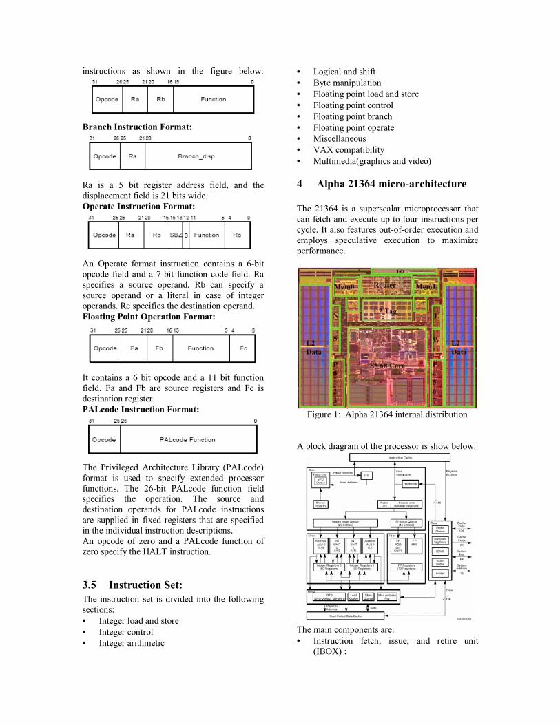
4 Alpha 21364 micro-architecture The 21364 is a superscalar microprocessor that can fetch and execute up to four instructions per cycle. It also features out-of-order execution and employs speculative execution to maximize performance.
Figure 1: Alpha 21364 internal distribution
A block diagram of the processor is show below:
The main components are: • Instruction fetch, issue, and retire unit
(IBOX) :
• Integer execution unit (EBOX) • Floating point execution unit (FBOX) • On chip caches (Icache and Dcache) • Memory reference unit (MBOX) • External cache and system interface unit
(CBOX)
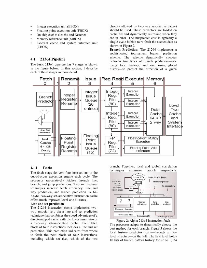
4.1 21364 Pipeline The basic 21364 pipeline has 7 stages as shown in the figure below. In this section, I describe each of these stages in more detail.
4.1.1 Fetch: The fetch stage delivers four instructions to the out-of-order execution engine each cycle. The processor speculatively fetches through line, branch, and jump predictions. Two architectural techniques increase fetch efficiency: line and way prediction, and branch prediction. A 64-Kbyte, two-way set-associative instruction cache offers much improved level-one hit rates. Line and set prediction The 21264 instruction cache implements two-way associatively via a line and set prediction technique that combines the speed advantage of a direct-mapped cache with the lower miss ratio of a two-way set-associative cache. Each fetch block of four instructions includes a line and set prediction. This prediction indicates from where to fetch the next block of four instructions, including which set (i.e., which of the two
choices allowed by two-way associative cache) should be used. These predictors are loaded on cache fill and dynamically re-trained when they are in error. The mispredict cost is typically a single-cycle bubble to re-fetch the needed data as shown in Figure 2. Branch Prediction: The 21264 implements a sophisticated tournament branch prediction scheme. The scheme dynamically chooses between two types of branch predictors�one using local history, and one using global history�to predict the direction of a given
branch. Together, local and global correlation techniques minimize branch mispredicts.
Figure 2: Alpha 21364 instruction fetch
The processor adapts to dynamically choose the best method for each branch. Figure 3 shows the local history prediction path�through a two-level structure�on the left. The first level holds 10 bits of branch pattern history for up to 1,024

branches. This 10-bit pattern picks from one of 1,024 prediction counters. The global predictor is a 4,096-entry table of 2-bit saturating counters indexed by the path, or global, history of the last 12 branches. The choice prediction, or chooser, is also a 4,096-entry table of 2-bit prediction counters indexed by the path history.
Figure 4: Block diagram of the 21264 tournament branch predictor. The local history prediction path is on the left; the global history prediction path and the chooser (choice prediction) are on the right. The accuracy of these predictors on most applications is in the range of 90-100%.
4.1.2 Register Renaming Register renaming exploits application instruction parallelism since it eliminates unnecessary dependencies (WAW and WAR) and allows speculative execution. It also preserves all RAW dependencies that are needed for correct computation. Register renaming assigns a unique storage location with each write-reference to a register. The 21264 speculatively allocates a register to each instruction with a register result.
Figure 4: Block diagram of the register rename
stage 41 integer and 41 floating-point registers are available to hold speculative results prior to instruction retirement. The register mapper stores the register map state for each in-flight instruction so that the machine architectural state can be restored in case a mis-speculation occurs. Also, an ID number is added to each instruction during this stage.
4.1.3 Instruction Issue The instructions from the queues are issued at this stage. The integer queue issues four instructions per cycle and the floating point one issue two. Issued instructions remain two more cycles in the queues. There are two instruction queues that issue instruction - a 20-entry integer and a 15-entry floating point. Each cycle the issue logic selects from the queued instructions when all their operands become available using register scoreboards.
4.1.4 Register Read The issued instructions read the necessary registers and receive bypassed data.
4.1.5 Execute The integer instructions are sent to the EBOX and the floating point instructions are sent to the FBOX pipeline. Figure 5 shows the four integer execution pipes (upper and lower for each of a left and right cluster) and the two floating-point pipes in the 21264, together with the functional units in each.
Figure 5: Four integer execution pipelines and
two floating point pipes together with the functional units in each
The integer register file is split into two clusters that contain duplicates of the 80-entry register file. Two pipes access a single register file to form a cluster, and the two clusters combine to support four-way integer instruction execution. This clustering makes the design simpler and faster, although it costs an extra cycle of latency to broadcast results from an integer cluster to the other cluster.

4.1.6 Memory Memory reference instructions access the Dcache and data translation buffers. Store data is written to the store queue where is held until the instruction retires. Instruction retire and exception handling Although instructions issue out of order, instructions are fetched and retired in order. The in-order retire mechanism maintains the illusion of in-order execution to the programmer even though the instructions actually execute out of order. The retire mechanism assigns each mapped instruction a slot in a circular in-flight window (in fetch order). After an instruction starts executing, it can retire whenever all previous instructions have retired and it is guaranteed to generate no exceptions. The retiring of an instruction makes the instruction nonspeculative. The 21264 implements a precise exception model using inorder retiring. The retire mechanism also tracks the internal register usage for all in-flight instructions. An exception causes all younger instructions in the in-flight window to be squashed. These instructions are removed from all queues in the system. The register map is backed up to the state before the last squashed instruction using the saved map state. The retire mechanism has a large, 80-instruction in-flight window. This means that up to 80 instructions can be in partial states of completion at any time, allowing for significant execution concurrency and latency hiding.
4.2 21364 Memory System: The memory system in the 21264 is high-bandwidth, supporting many in-flight memory references and out-of-order operation. It receives up to two memory operations (loads or stores) from the integer execution pipes every cycle. This means that the on-chip 64 KB two-way set-associative data cache is referenced twice every cycle, delivering 16 bytes every cycle. The L1 cache contains 64k bytes of data in 64-byte blocks with 2-way set associative placement, write back, and write allocate on a write miss. The data cache of the 21364 is show in Figure 6.
Figure 6: Organization of data cache
The L2 cache is six-way set associative with a size of 1.75MB. It has 16 GB bandwidth. The victim cache for L1 cache has 16 entries and that for L2 cache has 32 entries. The 21264 memory core logics up to 32 in-flight loads, 32 in-flight stores, 8 in-flight (64-byte) cache block fills, and 8 cache victims. This allows a high degree of parallel memory system activity to the cache and system interface. It translates into high memory system performance, even with many cache misses. The data path for the system is in Figure 7. Here we can see that the system also includes a speculative store data buffer. A store first writes into this buffer. The written data stays speculative until the store retires. Once this happens the data is dumped into the DCache.
Figure 7: The 21364�s internal memory system
data paths. The 21364 memory system supports the full capabilities of the out-of-order execution core, yet maintains an in-order architectural memory model. The 21364 provides cache prefetch instructions that allow the compiler and/or assembly programmer to take full advantage of the parallelism and high-bandwidth capabilities of the memory system. These prefetches are particularly useful in applications that have loops that reference large arrays.

4.3 Integrated Memory Controller: While previous processor generations were relying on an external support logic chip set for controlling the computer's memory, 21364 integrates two 800 MHz Direct RAMbus controllers onto the die. Each controller connects to 4 RDRAM channels. Integration of the memory controllers onto the processor die boosts the memory bandwidth to 12.8 GB/s and a 30 ns access latency for open memory pages.
4.4 Integrated Network Interface The Alpha 21364 processor provides a high-performance, highly scalable and highly reliable network architecture. The router runs at 1.2GHz and routes packets at a peak bandwidth of 22.4 GB/s. The network architecture scales up to a 128-processor configuration, which can support up to four terabytes of distributed RAMbus memory and hundreds of terabytes of disk storage. The distributed RAMbus memory is kept coherent via a scalable, directory-based, cache coherence scheme. The network architecture of the Alpha 21364 is shown in Figure 8.
Figure 8: Alpha 21364 network architecture
In order to make it easy to build large multiprocessor systems, 21364 contains an on-chip interface and router for a direct processor-to-processor interconnect. The interface consists of 4 32-bit ports with 6.4 GB/s bandwidth each and a 15 ns processor-to-processor latency. The interconnect forms a 2-D torus network that supports deadlock free adaptive routing in the integrated interface. The network interface autonomously handles all protocol transactions necessary to build a cache-coherent nun-uniform memory access (ccNUMA) shared memory multi-processor (SMP) system. An additional 5th port on the processor provides a similar interface to support an I/O channel with
6.4 GB/s bandwidth. Each network router provides buffer space for over 300 packets.
5 Memory Management The Alpha architecture uses a combination of segmentation and paging, providing protection while minimizing page table size. Virtual Address: The Alpha 21364 uses a 64 bit virtual address. The virtual address consists of three level-number fields and a byte_within_page field, as shown in Figure
The byte_within_page field can be either 13, 14, 15, or 16 bits depending on a particular implementation. Thus, the allowable page sizes are 8K bytes, 16K bytes, 32K bytes, and 64 Kbytes. Physical Address: Physical addresses are at most 48 bits. The two most significant implemented physical address bits delineate the four regions in the physical address space. Implementations use these bits as appropriate for their systems. Page Table Entries: The processor uses a quadword Page Table Entry (PTE), as shown in Figure to translate virtual addresses to physical addresses. A PTE contains hardware and software control information and the physical Page Frame Number.
I am not explaining all the fields of the PTE since they can easily be looked up in the manual. There are four processor modes � kernel, executive, supervisor and user mode.
5.1 Address Tranlation Physical address translation is performed by accessing entries in a multilevel page table structure. The Page Table Base Register (PTBR) contains the physical Page Frame Number (PFN) of the highest-level page table. Level1 is the highest-level page table. Bits <Level1> of the virtual address are used to index into the Level1 page table to obtain the physical PFN of the base of the next level (Level2) page table. Bits <Level2> of the virtual address are used to index into the Level2 page table to obtain the physical PFN of the base of the next level (Level3) page table. Bits <Level3> of the virtual address are used to index into the Level3 page table to obtain the physical PFN of the page being referenced. The PFN is concatenated with

virtual address bits <byte_within_page> to obtain the physical address of the location being accessed as shown in figure.
Figure 9: Virtual address mapping
In order to save actual memory references when repeatedly referencing the same pages, hardware implementations include a translation buffer to remember successful virtual address translations and page states. The overall picture of the Alpha 21364 memory hierarchy is shown in figure .I am not including a full description of the address translation. Interested readers can read about in the computer architecture book by Hennessy and Patterson. The reduced page table (RPT) mode is an optional extension of 64KB page size mode. A portion of the address space is mapped by one fewer page table levels, allowing each of the entries in the lowest-level page table to map a 512MB page. In implementations that support granularity hints in hardware, applications can use these hints to make more efficient use of the translation buffer.
6 I/O System Conceptually, Alpha systems consists of processors, memory, a processor-memory interconnect (PMI), I/O buses, bridges, and I/O devices. As shown in Figure 10, processors, memory, and possibly I/O devices, are connected by a PMI. A bridge connects an I/O bus to the system, either directly to the PMI or through another I/O bus. The I/O bus address space is available to the processor either directly or indirectly. Indirect access is provided through either an I/O mailbox or an I/O mapping mechanism. The I/O mapping mechanism includes provisions for mapping
between PMI and I/O bus addresses and access to I/O bus operations.
Fig 10: I/O System
Alpha I/O operations include: • Accesses between the processor and an I/O
device across the PMI • Accesses between the processor and an I/O
device across an I/O bus • DMA accesses � I/O devices initiating
reads and writes to memory • Processor interrupts requested by devices • Bus-specific I/O accesses
7 Analysis After studying the Alpha 21364 processor in some detail, I feel that it is very unfortunate that any future development of the Alpha processor has been stopped. Alpha microprocessors have consistently outperformed their contemporary processors in Spec benchmarks by a huge factor since their introduction in 1992. The reason for the failure of the Alpha series is DEC�s lack of enough infrastructure and marketing skills. Another reason for its failure is the outrageously high prices of these processors resulting in a low market demand. This has become a cycle where the low demand has kept the price high. In this section I try to analyze the strengths and weaknesses of the processor:
7.1 Strengths • Alpha was designed to have a life span of 25
years and was the first 64 bit ISA. Hence it used the latest ideas of the time and is easily extendible. The good thing was that the Alpha line of processors was totally different from DEC�s previous VAX architecture. This gave the designers lot of freedom to design a better architecture unlike some of the other big companies which carry around flaws in their architecture down many generations.
• High clock speeds. The first Alpha chip shipped in 1992, ran at a record-breaking 200MHz. Alpha was also the first mass-

produced chip to reach a clock speed of 1GHz in 1999.
• It is RISC to the extreme. All the instructions are very simple. No instruction takes more than a few clock cycles leading fewer stalls in the pipeline.
• Employs cutting edge technology including out-of-order, speculative and superscalar execution, high memory bandwidth, large memory support and high clock speed for high performance.
• A number of Alpha instructions include hints for implementations, all aimed at achieving higher speed. Calculated jump instructions have a target hint that can allow much faster subroutine calls and returns. There are prefetching hints for the memory system that can allow much higher cache hit rates. There are granularity hints for the virtual-address mapping that can allow much more effective use of translation lookaside buffers for large contiguous structures.
• PALcode implements some necessary low-level hardware support functions, which are too complex, too costly, or otherwise impractical to implement directly in the microprocessor chip�s hardware, and which cannot be handled by normal operating system software, including power-up initialization, memory management control, interrupt and exception dispatching. It thus allows designers to create their own code to support their Alpha microprocessor system designs. The use of PALcode eliminates the need for micro code.
• Extremely big on-processor cache. It has 128K L1 cache and an unbelievably huge 1.75MB on-chip L2 cache.
• Separate instruction and data cache: Having separate instruction and data cache result in a lower miss rate.
• Highly accurate line, way and branch predictors. This helps keep the pipeline 50-75% full at all times without any compiler optimizations.
• The Alpha processor aggressively prefetches instructions to keep the pipeline full at all times.
• Highly parallel execution � The Alpha processor is able to keep its pipeline full because of aggressive instruction fetch and accurate branch prediction. It is able to support 80 in flight instructions using a number of pipelined execution units and
registers. It uses a Tomasulo type approach for dynamic scheduling.
• Because Alpha does segmented paging, providing protection is easier.
• Extremely fast front and back side buses. • Highly scalable and fast microprocessor
systems. This is achieved by what is called �system on a chip� design. The chip has an integrated L2 Cache, integrated memory controller and an integrated network interface. The integrated L2 cache and memory controller result in outstanding single processor performance. The integrated network interface results in highly scalable, high performance multi-processor systems.
• Uses SMT for maximum utilization of function units by independent operations. They do this by replicating resources like program counters and increasing size of shared resources like instruction queue, L1 and L2 cache, TLB etc.
• The Alpha series of processors maintain full binary compatibility with earlier Alpha processors.
• Though I have not described the Alpha�s floating point performance in this report, it has been reported in many places that the Alpha�s floating point performance is excellent.
In 1999, the Alpha 21264 @ 700 MHz had scores of 39 and 68 on SPECINT95 and SPECFP95, while the comparable Intel Pentium III @ 733MHz had scores of only 36 and 30. Alpha�s floating point performance is far superior. The graphs below show the superior performance of the Alpha processor on both SPECINT95 and SPECFP95benchmarks.
Fig 10: Specint95 benchmark

Fig 11: Specfp95 benchmark
7.2 Weaknesses • Very expensive. This is partly because of the
huge on-chip L2 cache and partly because of DEC�s inability to mass-produce the processor like Intel.
• DEC�s first Alpha was a big deviation from their previous VAX architecture. Even though DEC management assured its customers of an upgrade path, it lost a huge customer base because of this radical change.
• Some essential instructions have been left out because it took more than a certain number of clock cycles. Sometimes, the series of simpler instructions took 2x as long to execute as the single complex instruction.
• Larger binary code because of the extreme RISC approach. Some results show that the series of simpler instructions are 50-100% larger than x86.
• The 64 bit architecture was way ahead of its time. This was at a time when there were no 64-bit compilers and other tools. This was one of the reasons why the Alpha architecture did not become very popular. However, the OpenVMS system became very popular later.
• The line and way predictors add to the complexity of the processor. An additional cycle is added to the load latency. However, the overall performance seems to improve because of the highly accurate prediction.
• The Alpha processor has a very aggressive speculation approach because of its highly accurate predictors. The penalty of a wrongly taken branch is quite high in some cases.
• I do not have the current feature size, but because of DEC�s lack of infrastructure, the Alpha was using a 0.35µm feature size when Intel and AMD were on 0.25µm feature size.
8 Conclusion The Alpha Architecture is an excellent example of a high performance architecture using many advanced techniques like out of order and speculative execution, high clock speeds and high bandwidth memory system. It is also a classic example of a superior architecture loosing out to competition.
9 References 1. John L Hennessy, David A Patterson,
Computer Architecture: A Quantitative Approach.
2. Alpha Architecture Reference Manual, Fourth Edition
3. 21264/EV68A Microprocessor Hardware Reference Manual.
4. Thomas Daniels, Dharmesh Parikh, Matt Ziegler, The Alpha 21264 ISA.
5. Artur Klauser, Trends in High-Performance Microprocessor Design
6. Zarka Cvetanovic and R.E. Kessler, Performance Analysis of the Alpha 21264 based compaq ES40 system.
7. Linley Gwennap, Digital 21264 Sets New Standard, Microprocessor Forum, Vol 10, No. 14
8. PALcode for Alpha Microprocessors, System Design Guide, May 1996
9. Shubhendu S. Mukherjee, Peter Bannon, Steven Lang, Aaron Spink, and David Webb, The Alpha 21364 Network Architecture
10. http://www.alphaprocessors.com 11. http://www3.sympatico.ca/n.rieck/links/dec_
memorial_site.html 12. http://web.singnet.com.sg/~duane/b1000005
.htm 13. http://h18020.www1.hp.com/alphaserver/per
formance/spec2000.html 14. http://www.macspeedzone.com/archive/4.0/
WinvsMacSPECint.html 15. http://www.extremetech.com/article2/0,3973
,1158263,00.asp 16. http://www.macinfo.de/hardware/chips-
top.html (Translated from german)
Related Documents