A radiation-tolerant A radiation-tolerant LDO voltage regulator LDO voltage regulator for HEP applications for HEP applications F.Faccio, P.Moreira, A.Marchioro, F.Faccio, P.Moreira, A.Marchioro, S.Velitchko S.Velitchko CERN CERN

Welcome message from author
This document is posted to help you gain knowledge. Please leave a comment to let me know what you think about it! Share it to your friends and learn new things together.
Transcript
A radiation-tolerant LDO A radiation-tolerant LDO voltage regulator for HEP voltage regulator for HEP
applicationsapplications
F.Faccio, P.Moreira, A.Marchioro, S.VelitchkoF.Faccio, P.Moreira, A.Marchioro, S.Velitchko
CERNCERN
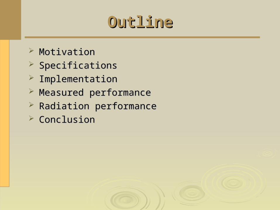
OutlineOutline
MotivationMotivation SpecificationsSpecifications ImplementationImplementation Measured performanceMeasured performance Radiation performanceRadiation performance ConclusionConclusion
MotivationMotivation
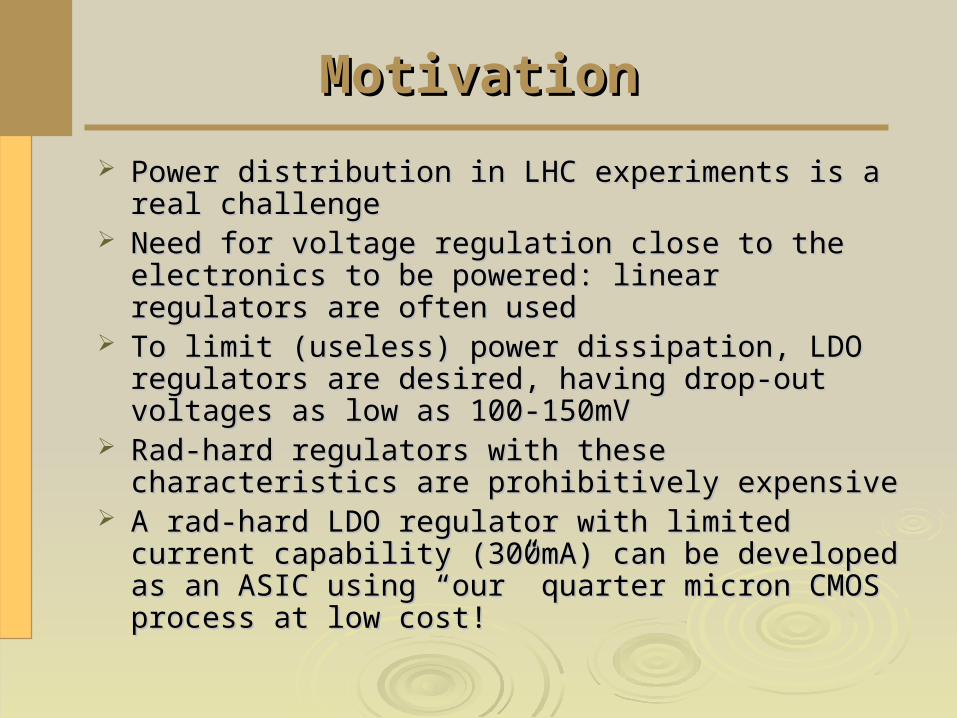
Power distribution in LHC experiments is a real Power distribution in LHC experiments is a real challengechallenge
Need for voltage regulation close to the electronics to Need for voltage regulation close to the electronics to be powered: linear regulators are often usedbe powered: linear regulators are often used
To limit (useless) power dissipation, LDO regulators To limit (useless) power dissipation, LDO regulators are desired, having drop-out voltages as low as 100-are desired, having drop-out voltages as low as 100-150mV150mV
Rad-hard regulators with these characteristics are Rad-hard regulators with these characteristics are prohibitively expensiveprohibitively expensive
A rad-hard LDO regulator with limited current A rad-hard LDO regulator with limited current capability (300mA) can be developed as an ASIC capability (300mA) can be developed as an ASIC using “our” quarter micron CMOS process at low cost!using “our” quarter micron CMOS process at low cost!

SpecificationsSpecifications
MinMin TypTyp MaxMax CommentComment
Output V (V)Output V (V) 2.52.5 Fixed in this versionFixed in this version
Input V (V)Input V (V) 2.652.65 2.72.7 3.53.5
Output I (mA)Output I (mA) 00 250250 300300
Dropout V (mV)Dropout V (mV) 150150 At 300mA currentAt 300mA current
Quiescent I (mA)Quiescent I (mA) 11
Over-V prot. (V)Over-V prot. (V) 3.53.5 Protects regulator itselfProtects regulator itself
Over-I prot. (mA)Over-I prot. (mA) 400400 600600 Switch to current regulationSwitch to current regulation
Over-T prot. (Over-T prot. (ooC)C) 150150 170170
Disable in/outDisable in/out yesyes Possible to disable, output Possible to disable, output flagflag

Implementation (1)Implementation (1)
Regulator named “CRTREG1”, as part of the CERN Regulator named “CRTREG1”, as part of the CERN Radiation Tolerant (CRT) family of componentsRadiation Tolerant (CRT) family of components
External compensation solution chosen: the dominant External compensation solution chosen: the dominant pole is the output polepole is the output pole
This imposes value (min. 1, suggested 6.6This imposes value (min. 1, suggested 6.6F) and F) and characteristics (low ESR of the order of 20mOhm) of characteristics (low ESR of the order of 20mOhm) of the output compensation capacitance, but allows for the output compensation capacitance, but allows for larger regulator bandwidth, hence good PSRR and larger regulator bandwidth, hence good PSRR and transient responsetransient response
Integrated in 0.25Integrated in 0.25m CMOS technology using m CMOS technology using radiation-tolerant layout techniquesradiation-tolerant layout techniques
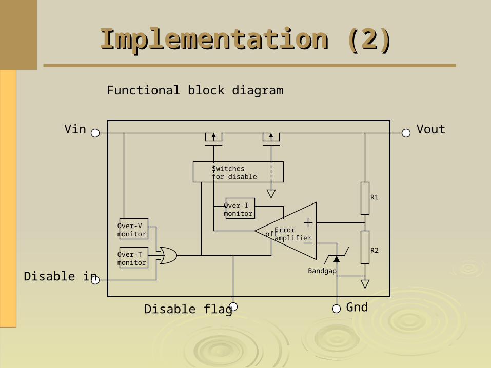
Implementation (2)Implementation (2)
Functional block diagram
offOver-Vmonitor
Over-Tmonitor
Switchesfor disable
Over-Imonitor
Error amplifier
R1
R2
Bandgap
Vin Vout
Gnd
Disable in
Disable flag

Implementation (3)Implementation (3)
Chip size: 2x2mmChip size: 2x2mm Multiple pads for input and output currentMultiple pads for input and output current Mounted on a very compact plastic package Mounted on a very compact plastic package
(4.9 x 6.1 x 1.6 mm), 16L-EPP-SSOP(4.9 x 6.1 x 1.6 mm), 16L-EPP-SSOP

Measured performanceMeasured performance
Samples packaged and Samples packaged and mounted on test boards, with mounted on test boards, with different output capacitors (to different output capacitors (to test transient response)test transient response)
10 samples measured10 samples measured
Quiescent current: 800Quiescent current: 800A at A at Vin=2.65V; 950Vin=2.65V; 950A at A at Vin=3.3VVin=3.3V
Output noise (Cout=6.6Output noise (Cout=6.6F), F), over full bandwidth:over full bandwidth:
170170V rms for I=0V rms for I=0 530530V rms for I=250mAV rms for I=250mA
CRTREG1 Cout
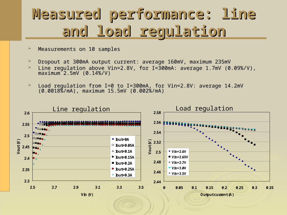
Measured performance: line and Measured performance: line and load regulationload regulation
Measurements on 10 samplesMeasurements on 10 samples
Dropout at 300mA output current: average 160mV, maximum 235mVDropout at 300mA output current: average 160mV, maximum 235mV Line regulation above Vin=2.8V, for I=300mA: average 1.7mV (0.09%/V), maximum 2.5mV Line regulation above Vin=2.8V, for I=300mA: average 1.7mV (0.09%/V), maximum 2.5mV
(0.14%/V)(0.14%/V)
Load regulation from I=0 to I=300mA, for Vin=2.8V: average 14.2mV (0.0018%/mA), Load regulation from I=0 to I=300mA, for Vin=2.8V: average 14.2mV (0.0018%/mA), maximum 15.5mV (0.002%/mA)maximum 15.5mV (0.002%/mA)
Line regulation Load regulation
2.3
2.35
2.4
2.45
2.5
2.55
2.6
2.5 2.7 2.9 3.1 3.3 3.5
Vin (V)
Vo
ut
(V) Iout=0A
Iout=0.05A
Iout=0.1A
Iout=0.15A
Iout=0.2A
Iout=0.25A
Iout=0.3A
2.44
2.46
2.48
2.5
2.52
2.54
2.56
2.58
0 0.05 0.1 0.15 0.2 0.25 0.3 0.35
Output current (A)
Vo
ut
(V)
Vin=2.6V
Vin=2.65V
Vin=2.7V
Vin=3.0V
Vin=3.5V
Measured performance: protectionsMeasured performance: protections
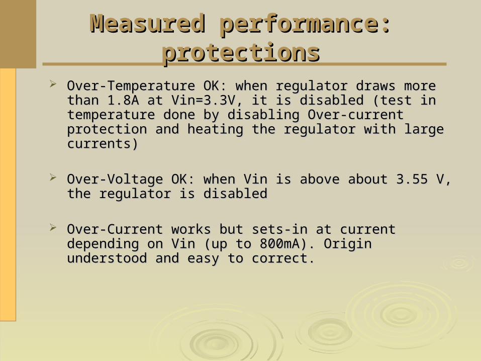
Over-Temperature OK: when regulator draws more than 1.8A at Over-Temperature OK: when regulator draws more than 1.8A at Vin=3.3V, it is disabled (test in temperature done by disabling Vin=3.3V, it is disabled (test in temperature done by disabling Over-current protection and heating the regulator with large Over-current protection and heating the regulator with large currents)currents)
Over-Voltage OK: when Vin is above about 3.55 V, the regulator Over-Voltage OK: when Vin is above about 3.55 V, the regulator is disabledis disabled
Over-Current works but sets-in at current depending on Vin (up Over-Current works but sets-in at current depending on Vin (up to 800mA). Origin understood and easy to correct.to 800mA). Origin understood and easy to correct.
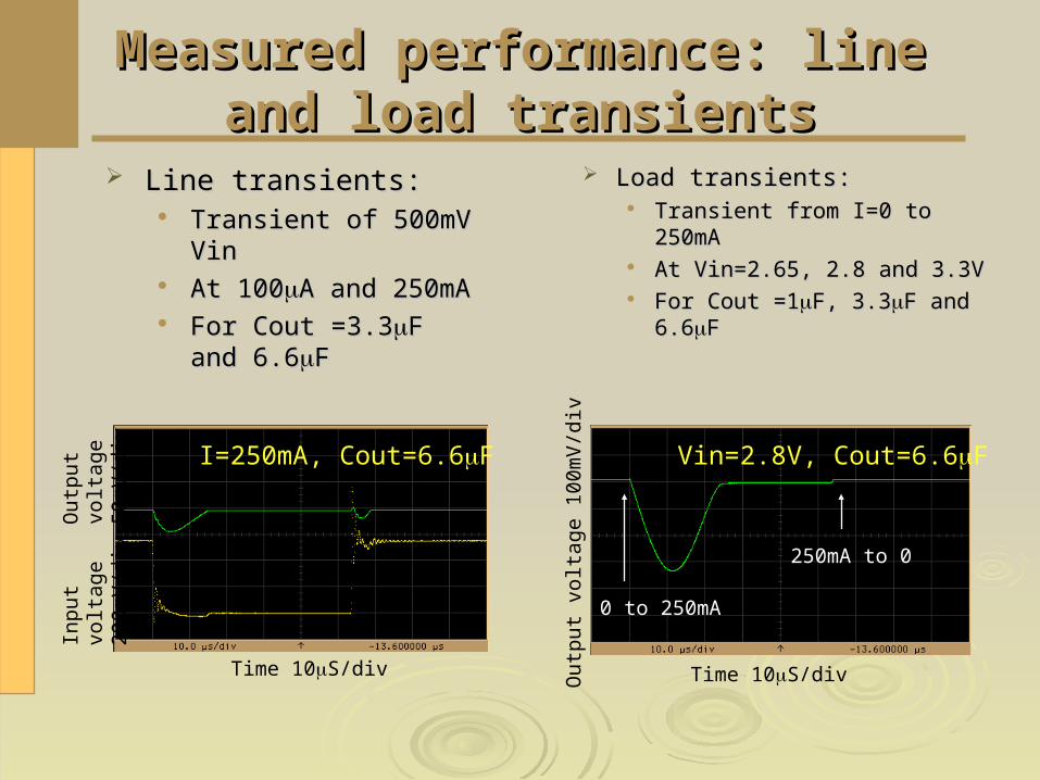
Measured performance: line and Measured performance: line and load transientsload transients
Line transients:Line transients: Transient of 500mV VinTransient of 500mV Vin At 100At 100A and 250mAA and 250mA For Cout =3.3For Cout =3.3F and F and
6.66.6FF
Load transients:Load transients: Transient from I=0 to 250mATransient from I=0 to 250mA At Vin=2.65, 2.8 and 3.3VAt Vin=2.65, 2.8 and 3.3V For Cout =1For Cout =1F, 3.3F, 3.3F and F and
6.66.6FF
Vin=2.8V, Cout=6.6F
Time 10S/div
Out
put
volta
ge 1
00m
V/d
iv
0 to 250mA
250mA to 0
I=250mA, Cout=6.6F
Out
put
volta
ge
50m
V/d
iv
Time 10S/div
Inpu
t vo
ltag
e 20
0m
V/d
iv

Measured performance: PSRRMeasured performance: PSRR
Power Supply Rejection measured injecting sine wave signal at Power Supply Rejection measured injecting sine wave signal at different frequency at the input (50-100mV peak-peak)different frequency at the input (50-100mV peak-peak)
Measurements for I=0 and 250mA, and for Cout=3.3Measurements for I=0 and 250mA, and for Cout=3.3F and F and 6.66.6FF
Vin=3VCout=6.6F
Able to filter effectively at full load up to 100kHz (similar regulators cut at 1kHz typically)
-90
-80
-70
-60
-50
-40
-30
-20
-10
0
1.E+00 1.E+02 1.E+04 1.E+06 1.E+08Frequency (Hz)
PS
SR
(d
B)
Load=0A
Load=250mA
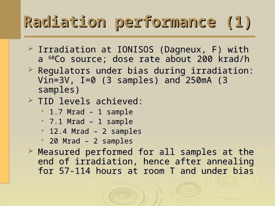
Radiation performance (1)Radiation performance (1)
Irradiation at IONISOS (Dagneux, F) with a Irradiation at IONISOS (Dagneux, F) with a 6060Co Co source; dose rate about 200 krad/hsource; dose rate about 200 krad/h
Regulators under bias during irradiation: Vin=3V, I=0 Regulators under bias during irradiation: Vin=3V, I=0 (3 samples) and 250mA (3 samples)(3 samples) and 250mA (3 samples)
TID levels achieved:TID levels achieved: 1.7 Mrad – 1 sample1.7 Mrad – 1 sample 7.1 Mrad – 1 sample7.1 Mrad – 1 sample 12.4 Mrad – 2 samples12.4 Mrad – 2 samples 20 Mrad – 2 samples20 Mrad – 2 samples
Measured performed for all samples at the end of Measured performed for all samples at the end of irradiation, hence after annealing for 57-114 hours at irradiation, hence after annealing for 57-114 hours at room T and under biasroom T and under bias
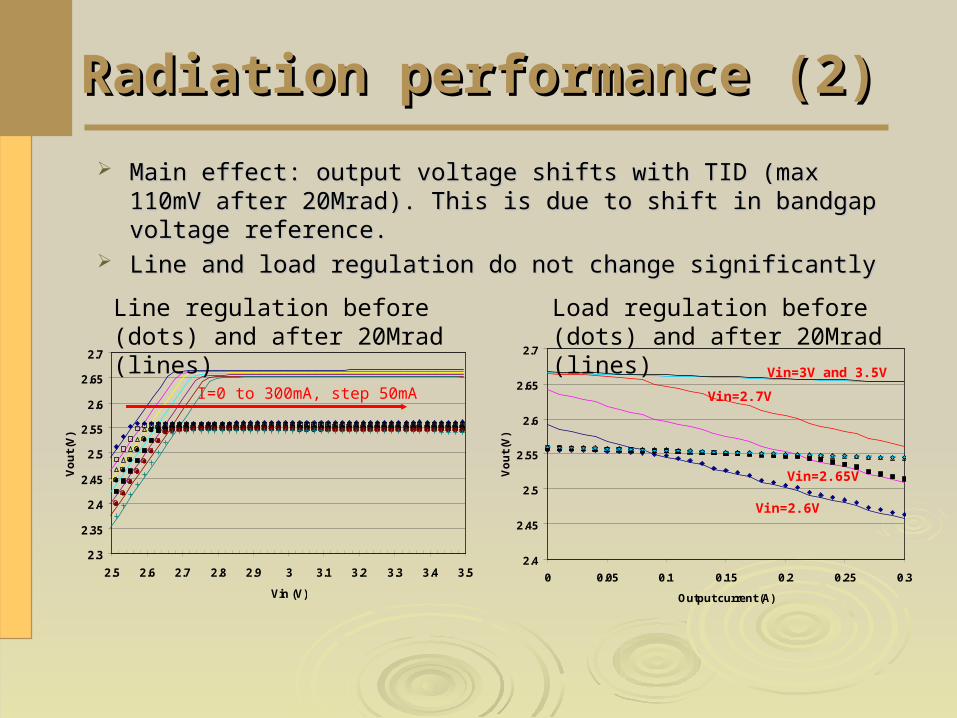
Radiation performance (2)Radiation performance (2)
Main effect: output voltage shifts with TID (max 110mV after Main effect: output voltage shifts with TID (max 110mV after 20Mrad). This is due to shift in bandgap voltage reference.20Mrad). This is due to shift in bandgap voltage reference.
Line and load regulation do not change significantlyLine and load regulation do not change significantly
2.3
2.35
2.4
2.45
2.5
2.55
2.6
2.65
2.7
2.5 2.6 2.7 2.8 2.9 3 3.1 3.2 3.3 3.4 3.5
Vin (V)
Vo
ut (
V)
Line regulation before (dots) and after 20Mrad (lines)
I=0 to 300mA, step 50mA
2.4
2.45
2.5
2.55
2.6
2.65
2.7
0 0.05 0.1 0.15 0.2 0.25 0.3
Output current (A)
Vo
ut
(V)
Load regulation before (dots) and after 20Mrad (lines)
Vin=2.6V
Vin=2.65V
Vin=2.7V
Vin=3V and 3.5V
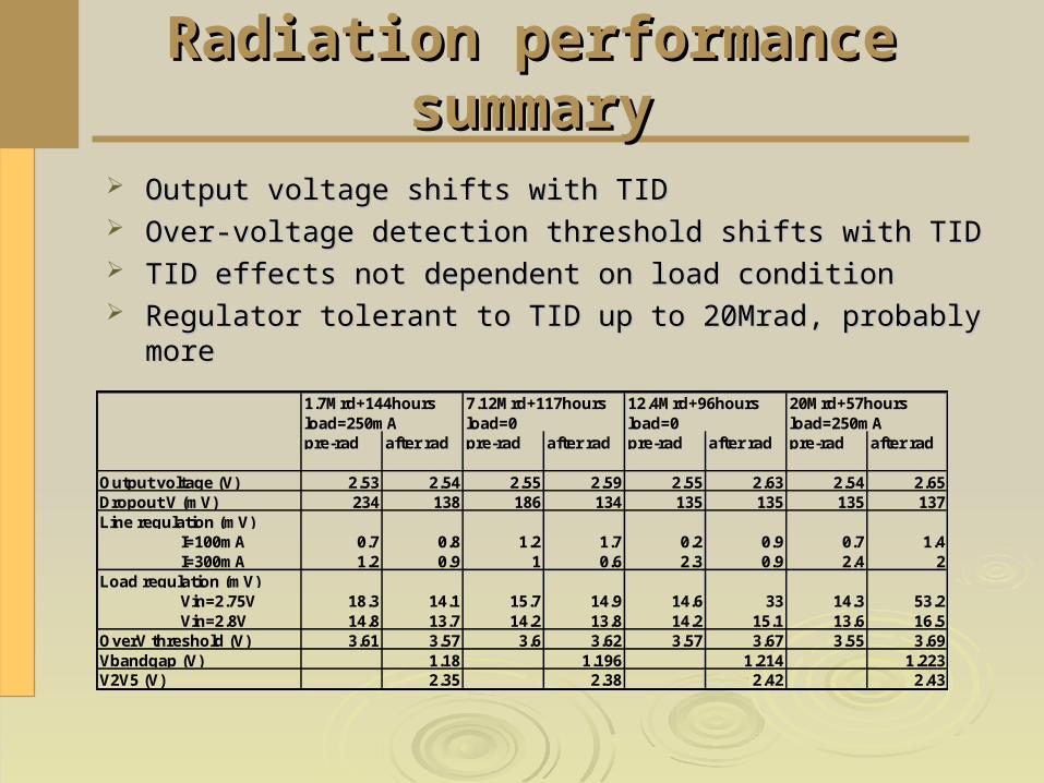
Radiation performance summaryRadiation performance summary
Output voltage shifts with TIDOutput voltage shifts with TID Over-voltage detection threshold shifts with TIDOver-voltage detection threshold shifts with TID TID effects not dependent on load conditionTID effects not dependent on load condition Regulator tolerant to TID up to 20Mrad, probably moreRegulator tolerant to TID up to 20Mrad, probably more
1.7Mrd+144hours 7.12Mrd+117hours 12.4Mrd+96hours 20Mrd+57hoursload=250mA load=0 load=0 load=250mApre-rad after rad pre-rad after rad pre-rad after rad pre-rad after rad
Output voltage (V) 2.53 2.54 2.55 2.59 2.55 2.63 2.54 2.65Dropout V (mV) 234 138 186 134 135 135 135 137Line regulation (mV)
I=100mA 0.7 0.8 1.2 1.7 0.2 0.9 0.7 1.4I=300mA 1.2 0.9 1 0.6 2.3 0.9 2.4 2
Load regulation (mV)Vin=2.75V 18.3 14.1 15.7 14.9 14.6 33 14.3 53.2Vin=2.8V 14.8 13.7 14.2 13.8 14.2 15.1 13.6 16.5
OverV threshold (V) 3.61 3.57 3.6 3.62 3.57 3.67 3.55 3.69Vbandgap (V) 1.18 1.196 1.214 1.223V2V5 (V) 2.35 2.38 2.42 2.43
ConclusionConclusion
CRTREG1, a compact LDO radiation-tolerant voltage CRTREG1, a compact LDO radiation-tolerant voltage regulator has been developedregulator has been developed
Its performance is well comparable to commercial Its performance is well comparable to commercial LDO regulators (dropout, line and load regulation, LDO regulators (dropout, line and load regulation, transient response, PSSR)transient response, PSSR)
First prototype fully working, easy correction to be First prototype fully working, easy correction to be implemented for better stability of over-current implemented for better stability of over-current protectionprotection
Radiation tolerance up to 20Mrad from Radiation tolerance up to 20Mrad from 6060Co source Co source has been demonstratedhas been demonstrated
The regulator is ready for productionThe regulator is ready for production
Related Documents