Rochester Institute of Technology Rochester Institute of Technology RIT Scholar Works RIT Scholar Works Theses 5-2021 A Programmable Processing-in-Memory Architecture for Memory A Programmable Processing-in-Memory Architecture for Memory Intensive Applications Intensive Applications Mark Connolly [email protected] Follow this and additional works at: https://scholarworks.rit.edu/theses Recommended Citation Recommended Citation Connolly, Mark, "A Programmable Processing-in-Memory Architecture for Memory Intensive Applications" (2021). Thesis. Rochester Institute of Technology. Accessed from This Thesis is brought to you for free and open access by RIT Scholar Works. It has been accepted for inclusion in Theses by an authorized administrator of RIT Scholar Works. For more information, please contact [email protected].

Welcome message from author
This document is posted to help you gain knowledge. Please leave a comment to let me know what you think about it! Share it to your friends and learn new things together.
Transcript

Rochester Institute of Technology Rochester Institute of Technology
RIT Scholar Works RIT Scholar Works
Theses
5-2021
A Programmable Processing-in-Memory Architecture for Memory A Programmable Processing-in-Memory Architecture for Memory
Intensive Applications Intensive Applications
Mark Connolly [email protected]
Follow this and additional works at: https://scholarworks.rit.edu/theses
Recommended Citation Recommended Citation Connolly, Mark, "A Programmable Processing-in-Memory Architecture for Memory Intensive Applications" (2021). Thesis. Rochester Institute of Technology. Accessed from
This Thesis is brought to you for free and open access by RIT Scholar Works. It has been accepted for inclusion in Theses by an authorized administrator of RIT Scholar Works. For more information, please contact [email protected].

A Programmable Processing-in-MemoryArchitecture for Memory Intensive Applications
Mark Connolly

A Programmable Processing-in-MemoryArchitecture for Memory Intensive Applications
Mark ConnollyMay 2021
A Thesis Submittedin Partial Fulfillment
of the Requirements for the Degree ofMaster of Science
inComputer Engineering
Department of Computer Engineering
A Programmable Processing-in-MemoryArchitecture for Memory Intensive Applications
Mark Connolly
Committee Approval:
Dr. Amlan Ganguly Advisor DateDepartment Head
Mark Indovina DateSenior Lecturer
Dr. Cory Merkel DateAssistant Professor
i
Abstract
While both processing and memory architectures are rapidly improving in per-
formance, memory architecture is lagging behind. As performance of processing ar-
chitecture continues to eclipse that of memory, the memory architecture continues
to become an increasingly unavoidable bottleneck in computer architecture. There
are two drawbacks that are commonly associated with memory accesses: i) large de-
lays causing the processor to remain idle waiting on data to become available and
ii) the power consumption required to transfer the data. These performance issues
are especially notable in research and enterprise computing applications such as deep
learning models. Even when data for an application such as this is transferred to a
cache before processing to avoid the delay, the large power cost of the transfer is still
incurred.
Processing-in-memory (PIM) architectures offer a solution to the issues in modern
memory architecture. The inclusion of processing elements within the memory archi-
tecture reduces data transfers between the host processor and memory, thus reducing
penalties incurred by memory accesses. The programmable-PIM (pPIM) architec-
ture is a novel PIM architecture that delivers the performance enhancements of PIM
while delivering a high degree of reprogrammability through the use of look-up tables
(LUTs).
A novel instruction set architecture (ISA) for the pPIM architecture facilitates
the architecture’s reprogrammability without large impacts on performance. The
ISA takes a microcoded approach to handling the control signals of the pPIM control
signals. This approach allows variable-stage instructions at a low additional cost to
the overall power and area of the architecture.
The versatility of the pPIM architecture enables MAC operations and several
common activation functions to be modeled for execution on the architecture. As a
measure of performance, post-synthesis models of both the pPIM architecture and the
ii
ISA are generated for CNN inference. As a proof-of-concept an FPGA model of the
pPIM architecture is developed for representations of a single layer neural network
(NN) model for classification of MNIST images.
iii

Contents
Signature Sheet i
Abstract ii
Table of Contents iv
List of Figures vi
List of Tables 1
1 Introduction 2
1.1 Motivation . . . . . . . . . . . . . . . . . . . . . . . . . . . . . . . . . 2
2 Background 5
2.1 Processing-in-Memory . . . . . . . . . . . . . . . . . . . . . . . . . . 5
2.2 Instruction Set Architectures . . . . . . . . . . . . . . . . . . . . . . . 7
2.3 Neural Networks . . . . . . . . . . . . . . . . . . . . . . . . . . . . . 8
2.4 Supporting Work . . . . . . . . . . . . . . . . . . . . . . . . . . . . . 10
3 pPIM Architecture 11
3.1 pPIM Core . . . . . . . . . . . . . . . . . . . . . . . . . . . . . . . . 12
3.2 pPIM Cluster . . . . . . . . . . . . . . . . . . . . . . . . . . . . . . . 13
3.3 pPIM Function Word Generation . . . . . . . . . . . . . . . . . . . . 14
3.4 pPIM MAC Operations . . . . . . . . . . . . . . . . . . . . . . . . . . 14
3.5 pPIM Activation Operations . . . . . . . . . . . . . . . . . . . . . . . 17
3.6 FPGA Implementation . . . . . . . . . . . . . . . . . . . . . . . . . . 20
3.6.1 Technology & Resources . . . . . . . . . . . . . . . . . . . . . 20
3.6.2 Machine Learning Model . . . . . . . . . . . . . . . . . . . . . 21
3.6.3 pPIM Implementation . . . . . . . . . . . . . . . . . . . . . . 21
3.6.4 Communication . . . . . . . . . . . . . . . . . . . . . . . . . . 22
3.7 Results . . . . . . . . . . . . . . . . . . . . . . . . . . . . . . . . . . . 23
3.7.1 pPIM Characteristics . . . . . . . . . . . . . . . . . . . . . . . 23
3.7.2 Performance Evalution . . . . . . . . . . . . . . . . . . . . . . 24
3.7.3 FPGA Characteristics . . . . . . . . . . . . . . . . . . . . . . 26
3.7.4 FPGA Performance Evaluation . . . . . . . . . . . . . . . . . 27
iv
CONTENTS
4 pPIM Instruction Set Architecture 28
4.1 ISA Communication . . . . . . . . . . . . . . . . . . . . . . . . . . . 29
4.2 pPIM Microcode . . . . . . . . . . . . . . . . . . . . . . . . . . . . . 29
4.3 pPIM Instruction Formatting . . . . . . . . . . . . . . . . . . . . . . 31
4.4 pPIM ISA Operation Mapping . . . . . . . . . . . . . . . . . . . . . . 32
4.5 FPGA Implementation . . . . . . . . . . . . . . . . . . . . . . . . . . 34
4.5.1 Technology & Resources . . . . . . . . . . . . . . . . . . . . . 34
4.5.2 ISA Implementation . . . . . . . . . . . . . . . . . . . . . . . 35
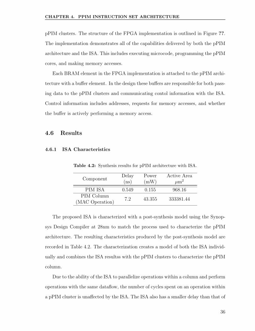
4.6 Results . . . . . . . . . . . . . . . . . . . . . . . . . . . . . . . . . . . 36
4.6.1 ISA Characteristics . . . . . . . . . . . . . . . . . . . . . . . . 36
4.6.2 FPGA Characteristics . . . . . . . . . . . . . . . . . . . . . . 38
5 Conclusions & Future Work 40
5.1 Future Work . . . . . . . . . . . . . . . . . . . . . . . . . . . . . . . . 41
Bibliography 42
v
List of Figures
1.1 The growing divide between processor speeds and memory bandwidth
that leads to a throttling of processor performance [1] . . . . . . . . . 3
2.1 The various types of processing with respect to their interaction with
memory. Traditional architectures include a cache coupled with proces-
sors. More recent architectures have attempted to reduce the distance
of memory from the processing power to reduce delays with ’near mem-
ory’ approaches. PIM goes a step beyond and introduces the processing
power within the memory architecture for further reduced latencies[2]. 6
3.1 Heirarchical view of the pPIM architecture . . . . . . . . . . . . . . . 11
3.2 Layout of the pPIM core architecture. . . . . . . . . . . . . . . . . . . 12
3.3 Layout of the pPIM cluster architecture. . . . . . . . . . . . . . . . . 13
3.4 Calculation of the result of an unsigned multiplication through the
calculation and summation of partial products. . . . . . . . . . . . . . 15
3.5 Model of dataflow within a pPIM cluster for both (a) 8-bit full precision
and (b) 4-bit half precision unsigned MAC operations . . . . . . . . . 15
3.6 Calculation of the result of a signed multiplication through the calcu-
lation and summation of partial products. . . . . . . . . . . . . . . . 16
3.7 Model of dataflow within a pPIM cluster for both (a) 8-bit full precision
and (b) 4-bit half precision signed MAC operations . . . . . . . . . . 17
3.8 Model of dataflow within a pPIM cluster for both (a) 16-bit precision
and (b) 8-bit precision ReLu activation operations. . . . . . . . . . . 18
3.9 Model of dataflow within a pPIM cluster for both (a) 16-bit precision
and (b) 8-bit precision saturated ReLu activation operations. . . . . . 18
3.10 Configuration of a pPIM cluster for quick switching between activation
operations. . . . . . . . . . . . . . . . . . . . . . . . . . . . . . . . . . 19
3.11 Model of dataflow within a pPIM cluster for a 16-bit max-index oper-
ation. . . . . . . . . . . . . . . . . . . . . . . . . . . . . . . . . . . . . 19
3.12 Structure of the multiple region approach to designing an FPGA im-
plementation of the pPIM architecture. . . . . . . . . . . . . . . . . . 22
3.13 Communication model between multiple elements within the ZC702
evaluation board and the host CPU. . . . . . . . . . . . . . . . . . . 22
vi
LIST OF FIGURES
3.14 Comparison of various high-performance architectures on their through-
put with popular deep learning models. . . . . . . . . . . . . . . . . . 24
3.15 Layout of the pPIM cluster architecture. . . . . . . . . . . . . . . . . 25
3.16 Layout of the pPIM cluster architecture. . . . . . . . . . . . . . . . . 25
3.17 Predictions made by the pPIM architecture running on the ZC702 base
board. . . . . . . . . . . . . . . . . . . . . . . . . . . . . . . . . . . . 27
4.1 Proposed ISA for handling control signals and memory accesses of the
pPIM architecture. . . . . . . . . . . . . . . . . . . . . . . . . . . . . 28
4.2 Model of interface between the ISA with pPIM Clusters and memory
elements. . . . . . . . . . . . . . . . . . . . . . . . . . . . . . . . . . . 29
4.3 ISA . . . . . . . . . . . . . . . . . . . . . . . . . . . . . . . . . . . . . 30
4.4 Formatting of instruction sent from host CPU to pPIM ISA. . . . . . 31
4.5 Timing example of two consecutive MAC operations performed on a
pPIM cluster by the pPIM ISA. . . . . . . . . . . . . . . . . . . . . . 34
4.6 Timing example of two consecutive MAC operations performed on a
pPIM cluster by the pPIM ISA. . . . . . . . . . . . . . . . . . . . . . 35
4.7 Comparison of power consumption of the ISA and pPIM clusters in
various deep learning models. . . . . . . . . . . . . . . . . . . . . . . 37
4.8 Comparison of throughput for inference on Alexnet. . . . . . . . . . . 38
vii
List of Tables
3.1 Synthesis results for pPIM architecture. . . . . . . . . . . . . . . . . . 23
3.2 Synthesis results for FPGA implementation . . . . . . . . . . . . . . 26
3.3 Timing results for FPGA implementation . . . . . . . . . . . . . . . . 27
4.1 Microcode Sequences . . . . . . . . . . . . . . . . . . . . . . . . . . . 33
4.2 Synthesis results for pPIM architecture with ISA. . . . . . . . . . . . 36
4.3 Synthesis results for FPGA implementation of pPIM ISA . . . . . . . 38
1 List of Publications and Submissions on pPIM Architecture . . . . . . 43
1

Chapter 1
Introduction
1.1 Motivation
Computer architecture is continually pushing to improve their performance where
possible. Most of this improvement is focused on the improvement of computer pro-
cessors which improve at a rate of approximately 60 percent every year. Meanwhile,
Dynamic random-access memory (DRAM) architecture is only improving at a rate
of 10 percent every year [3]. The large difference in improvements made leads to a
growing divide that throttles the overall computer system’s performance. Still, the
main focus of DRAM architectural design is on reducing sizes and increasing capaci-
ties. The differing focus of these two groups continually increases the divide between
performance improvement at an exponential rate creating a problem that is com-
monly referred to as the ”memory wall”[4]. The ”memory wall” is best defined by a
growing divide between processing power and memory bandwidth, depicted in Figure
1.1. This has lead to multiple improvements that remedy the issue brought on by
this ”memory wall”. The memory wall has become so prevalent that the avoidance
of it has driven a great deal of research and innovations.
When a miss occurs that requires memory access there are multiple downsides
that can occur. The most commonly considered downside is the delay that occurs.
In the case that a miss occurs, several communications are required with memory in
2
CHAPTER 1. INTRODUCTION
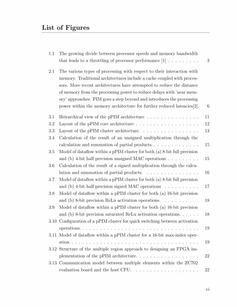
Figure 1.1: The growing divide between processor speeds and memory bandwidth thatleads to a throttling of processor performance [1]
addition to the desired data. This can lead to delays that could take hundreds of
cycles. Each memory access also incurs a large power cost to transfer the data from
the DRAM over to the processor. The power required for this data transfer can reach
up to 42% [5] of the total power cost. Even if the data is transferred over to the
memory before it is accessed, the downside of the power cost for the data transfer is
still incurred on the system. Each of these problems become especially burdensome
with data-intensive applications such as machine learning models that require large
transfers of data to be processed.
While the average consumer might not see heavy impacts of delays from mem-
ory accesses, enterprise and research computing frequently collide with the ”memory
wall”. Commercial and scientific computing will often deal with much larger quanti-
ties of data that the average consumer which can present itself in various ways. These
applications can vary from large databases of user data to datasets and weight infor-
mation for training machine learning models. This causes commercial and scientific
computing to see idle times that average around 65 percent and 95 percent[1].
With the bottleneck of the ”memory wall” approaching and increase in data-
3
CHAPTER 1. INTRODUCTION
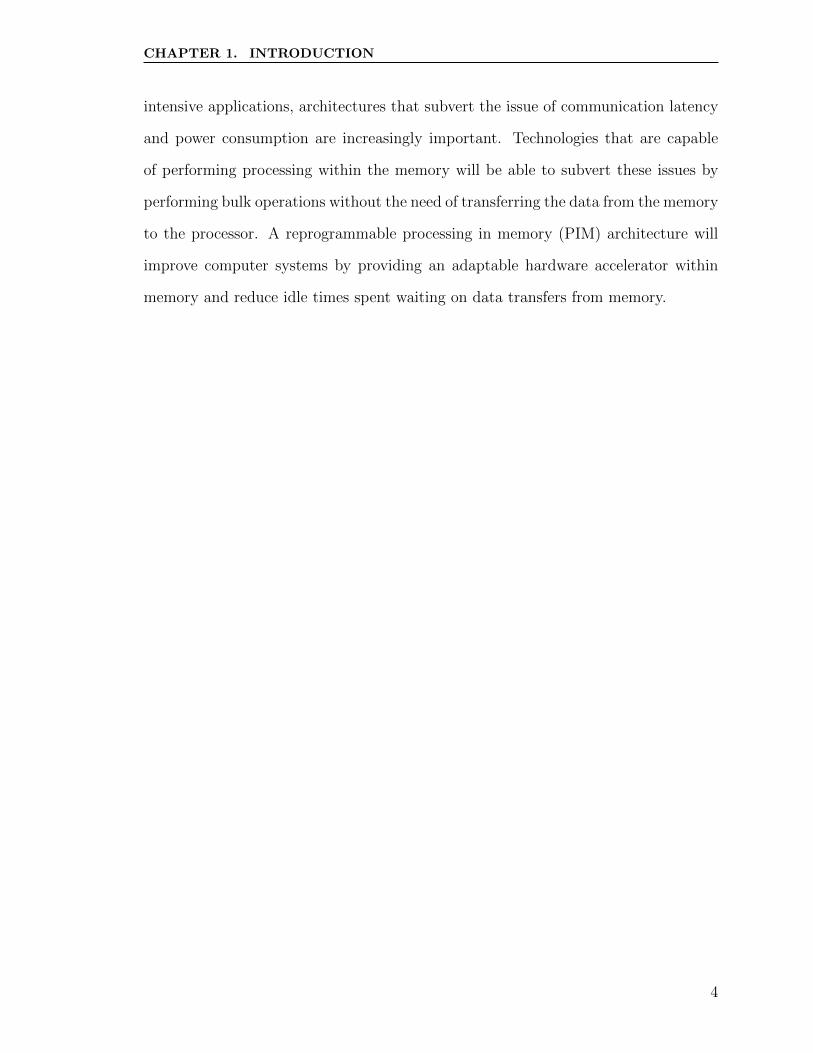
intensive applications, architectures that subvert the issue of communication latency
and power consumption are increasingly important. Technologies that are capable
of performing processing within the memory will be able to subvert these issues by
performing bulk operations without the need of transferring the data from the memory
to the processor. A reprogrammable processing in memory (PIM) architecture will
improve computer systems by providing an adaptable hardware accelerator within
memory and reduce idle times spent waiting on data transfers from memory.
4
Chapter 2
Background
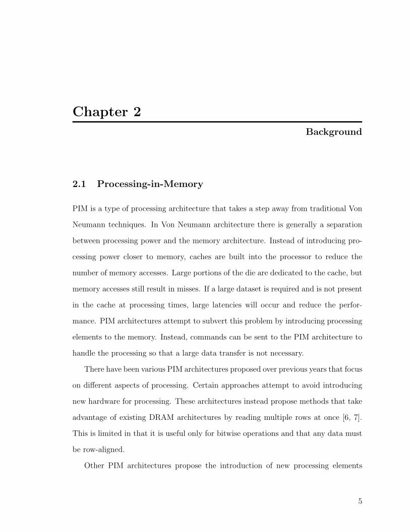
2.1 Processing-in-Memory
PIM is a type of processing architecture that takes a step away from traditional Von
Neumann techniques. In Von Neumann architecture there is generally a separation
between processing power and the memory architecture. Instead of introducing pro-
cessing power closer to memory, caches are built into the processor to reduce the
number of memory accesses. Large portions of the die are dedicated to the cache, but
memory accesses still result in misses. If a large dataset is required and is not present
in the cache at processing times, large latencies will occur and reduce the perfor-
mance. PIM architectures attempt to subvert this problem by introducing processing
elements to the memory. Instead, commands can be sent to the PIM architecture to
handle the processing so that a large data transfer is not necessary.
There have been various PIM architectures proposed over previous years that focus
on different aspects of processing. Certain approaches attempt to avoid introducing
new hardware for processing. These architectures instead propose methods that take
advantage of existing DRAM architectures by reading multiple rows at once [6, 7].
This is limited in that it is useful only for bitwise operations and that any data must
be row-aligned.
Other PIM architectures propose the introduction of new processing elements
5
CHAPTER 2. BACKGROUND
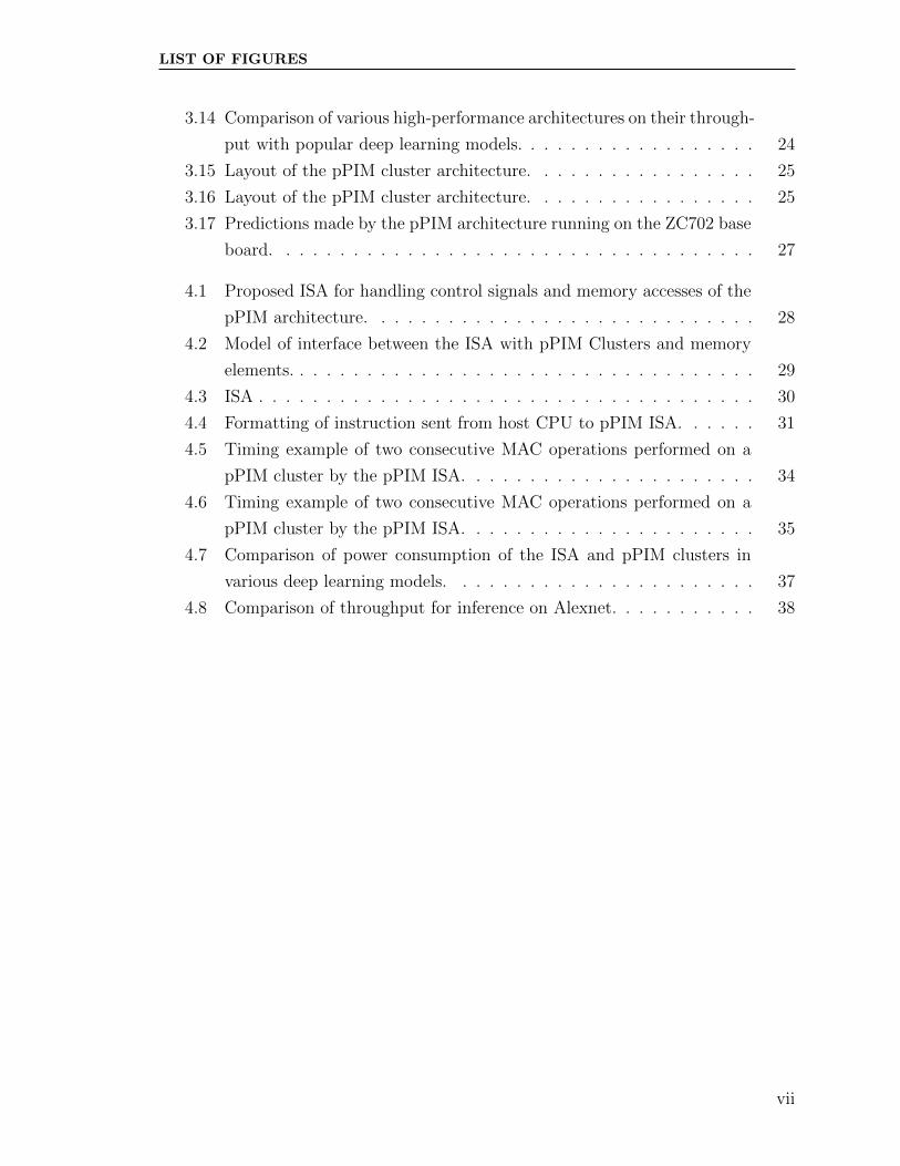
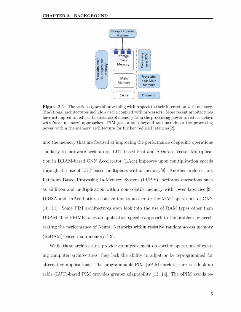
Figure 2.1: The various types of processing with respect to their interaction with memory.Traditional architectures include a cache coupled with processors. More recent architectureshave attempted to reduce the distance of memory from the processing power to reduce delayswith ’near memory’ approaches. PIM goes a step beyond and introduces the processingpower within the memory architecture for further reduced latencies[2].
into the memory that are focused at improving the performance of specific operations
similarly to hardware acclerators. LUT-based Fast and Accurate Vector Multiplica-
tion in DRAM-based CNN Accelerator (LAcc) improves upon multiplication speeds
through the use of LUT-based multipliers within memory[8]. Another architecture,
Latch-up Based Processing In-Memory System (LUPIS), performs operations such
as addition and multiplication within non-volatile memory with lower latencies [9].
DRISA and DrAcc both use bit shifters to accelerate the MAC operations of CNN
[10, 11]. Some PIM architectures even look into the use of RAM types other than
DRAM. The PRIME takes an application specific approach to the problem by accel-
erating the performance of Neural Networks within resistive random access memory
(ReRAM)-based main memory [12].
While these architectures provide an improvement on specific operations of exist-
ing computer architectures, they lack the ability to adpat or be reprogrammed for
alternative applications. The programmable-PIM (pPIM) architecture is a look-up
table (LUT)-based PIM provides greater adaptability [13, 14]. The pPIM avoids re-
6

CHAPTER 2. BACKGROUND
stricting the user to accelerating specific functions by allowing the reconfiguration of
LUTs with function words. The pPIM architecture has been published previously in
Computer Architecture Letters(CAL) and is currently submitted with minor revisions
for Transactions on Parallel and Distributed Systems (TPDS).
2.2 Instruction Set Architectures
The instruction set architecture (ISA) associated with a hardware is an integral com-
ponent that bridges the gap between the hardware and the software applications
that can be used with the hardware. DUe to the nature of both memory and PIM
these ISAs are designed to take instructions from external host processors[15, 16, 17].
Memory is already a passive element that operates off instruction from an external
hoss[18]. Implemention of an ISA with memory will see less difficulty if the ISA also
has a passive design. Additionally, PIM architecture is often focused on accelerating
big data applications, such as neural networks, which often perform repetitive opera-
tions over bulk quantities of data[2, 19]. An ISA for PIM should reflect this focus of
the architecture. Instead of executing entire programs the ISA should be focused on
accelerating computations required by the host in a single-instruction multiple-data
manner. It is also important to design a PIM ISA with a low level of complexity. If
the ISA becomes too complex, the ISA could take up large swaths of area or power
and become too costly to reasonably include within the DRAM.
Microcode offers a viable solution to the problem of over complexity and area.
Microcode is a form of programming that is done at the control signal level. This
form of coding is capable of performing operations that otherwise would require the
introduction of new hardware. Microcode usage for an ISA is especially useful in
the DRAM where a reduction in the hardware will reduce the area that will be taken
from the DRAM memory to integrate the component. Instead of using physical space
required for hardware copmonents of the ISA, the microcode of a PIM architecture
7
CHAPTER 2. BACKGROUND
could be stored into the memory. This also allows for a reprogrammable ISA that
can be changed to suit the needs of the host processor.
2.3 Neural Networks
Neural networks are abundantly common in machine learning models for their abil-
ity to perform classification. These layers appear in varying formats such as dense
layers and convolutional neural networks. These variations do have in common that
they perform matrix multiplications on datasets that are often large in size. Perform-
ing such an operation requires that a multiply accumulate operations be repeated
throughout the datasets and the weights of the model.
Other components involved with neural networks in machine learning models in-
clude the functions used for classification and activation. Classification of the final
output layer can be done by determining the index of max value in the set.
The activation layer of a neural network is used to remove the linear relationship
between the input and the output of a neural network layer. If a linear activation layer
is used, displayed in Equation 2.3, the output will maintain a linear relationship with
the input and not necessarily be the best representation of the relationship between
the input and the expected output. Non-linear relationships are used to avoid this
problem when training neural networks. Some of the most common activation layers
being sigmoid, tanh, and Rectified Linear Unit (ReLU).
f(x) = x (2.1)
Equation 2.3 depicts the sigmoid activation function that scales an output between
0 and 1. With the range from 0 to 1, the output can be interpreted similar to a
probability which is useful in a classification. Due to the high derivative in the center
8
CHAPTER 2. BACKGROUND
of the functions, the model is also very useful in training. In backpropagation, the
high derivative forces the weights towards the extremes.
f(x) =1
1 + e−x(2.2)
The tanh is a trigonometrical activation function that improves upon the sigmoid
function. Instead of scaling to a range from 0 to 1, the tanh function scales from a
range from -1 to 1. This is useful in classifications where the presence of a certain
input may lead to strong confidence that a classification should not be made.
The ReLU activation function was introduced due to the high complexity of the
sigmoid and tanh activation functions that led to longer training times. ReLU takes
the simplicity of the linear unit and introduces a non-linear behavior to the function
by rectifying it, or producing an output of 0 for any negative input.
f(x) = max(0, x) (2.3)
The ReLU activation is currently one of the most commonly used activation lay-
ers in neural networks. The ReLU activation activation, depicted in Equation 2.3,
requires very little computation power. Since the only operation it performs is setting
negative values to zero, it often leads to quicker training. It also will also often output
sparse matrices, which are matrices with a large presence of zeros throughout it.
The tanh function is an activation that is used to scale the outputs of a layer to
a value between -1 and 1.
9
CHAPTER 2. BACKGROUND
2.4 Supporting Work
Introducing a PIM architecture can often be difficult due to the lack of existing
architecture that leaves DRAM in a position to under-perform in processing. One
reason for this is the lack of existing architecture for efficient data movement among
subarrays. It is restricting for a PIM architecture to be limited to only using the data
within a single subarray. Even with access to data external to the coupled subarray,
data accesses can be costly in terms of power and latency. RowClone tackles this
issue by proposing an efficient method for copying bulk data between subarrays at
low energy cost [5]. Low-Cost Inter-Linked Subarrays (LISA) further expands on the
RowClone architecture by proposing an architecture that is capable of providing fast
memory copying between subarrays at low cost to power[20].
Introducing a PIM architecture must also provide a sufficient boost in the perfor-
mance that provides a benefit to a system. A design that is either slow or has a high
power will likely diminish the performance benefits that are produced by reducing
the memory transfer between the host and memory. For this reason, LUTs have been
frequently used in PIM designs. LUTs have shown that they are capable of produc-
ing fast designs at low power costs[11, 10, 8]. The use of LUTs can also provide
reconfigurability to a design so that it can be adapted to multiple applications.
10

Chapter 3
pPIM Architecture
Subarray Interlinks
Subarray
Subarray Interlinks
Subarray
Local Row Buffer
Local Row Buffer
Cluster Cluster Cluster
Cluster Cluster Cluster
Core 1
Core 2
Core 9
Exte
nded
Bitl
ines
Read Ptr.
WritePtr.
R/ W
Buf
fer
DRAM Bank
pPIM Cluster
A
B
n= 0,1, 2 ... 12; n ≠ k
Core k/ Acc
4 n:1 MUX
n:1 MUX
Core 1
Core 2
Cluster Router C
Router
Function-word
Function-word
Function-word
Function-word
LUT Core
FromBitlines
Reg A
Reg B
256:1
Router
D
256:1
4
8
256
I/O
Acc.
Figure 3.1: Heirarchical view of the pPIM architecture
The proposed pPIM architecture’s is a PIM architecture design focuses on per-
forming data-intensive applications. The hierarchy of the proposed architecture is
depicted in Figure 3.1. An additional goal of the design is to be reprogrammable to
fit a wide variety of applicatinos. The design accomplishes this in architecture with
a LUT-based design. The pPIM architecture consists of a pPIM cluster at the top
level. Within each cluster are multiple pPIM cores that enable reprogrammability
within the architecture.
11

CHAPTER 3. PPIM ARCHITECTURE
3.1 pPIM Core
Figure 3.2: Layout of the pPIM core architecture.
The base processing element of the pPIM architecture is the pPIM core. The
design of the pPIM core is shown in Figure 3.2. The pPIM core is responsible for
a majority of the computational power within the pPIM architecture. Processing
within the core is handled through the congregation of LUTs into multiplexers. A
majority of the reprogrammability is also handled within the pPIM core through the
use of a register file that feeds into the LUTs.
Various functions are capable of being represented by the pPIM core. A function
that is capable of being programmed into the pPIM core is any function that consists
of two 4-bit inputs and a single 8-bit output. The two inputs can also be treated as
a high and low segment of the input if a function contains a single operand. This
functionality is accomplished by the pPIM core through the use of an array of LUTs
that form eight 256-to-11 multiplexers. Input to the multiplexers is determined by
the data within the register file of the pPIM core. Conversely, the select lines of the
multiplexers are determined by the two input vectors to the pPIM core.
Within the pPIM core’s register file are eight function words. Each of the function
words are eight bits in length to fit the input to the 256-to-1 multiplexers. Each of
12

CHAPTER 3. PPIM ARCHITECTURE
the functions words are then associated with a single bit position within the output
of the pPIM core.
3.2 pPIM Cluster
Figure 3.3: Layout of the pPIM cluster architecture.
At the top level of the pPIM cluster is the pPIM cluster. The structure of the pPIM
cluster is displayed in Figure 3.3. The pPIM cluster combines the use of multiple pPIM
cores, interconnected by a router. Combining functionality of multiple pPIM cores
allows the pPIM cluster to perform more complex operations over a single or multiple
stages. The added functionality includes performing operations that require greater
resolution than the inputs and operations that require more than two operands.
Each pPIM cluster contains nine pPIM cores that that provide computational
power. The pPIM cores within a pPIM cluster are individually programmed, max-
imizing the flexibility of the design to adapt to various applications. The dataflow
within the pPIM cluster requires an all-to-all communication network with minimal
13
CHAPTER 3. PPIM ARCHITECTURE
overhead. This is accomplished through the use of a crossbar switch architecture.
Through the use of a crossbar switch routing architecture, each pPIM core can re-
ceive input from the outputs of any other pPIM core within the pPIM cluster. To
match the size of the inputs and outputs of the pPIM cores within the routing archi-
tecture, the 8-bit outputs are treated as two 4-bit segments.
3.3 pPIM Function Word Generation
Adaptation of a pPIM core to perform a specific function requires the generation of
eight function words. This requires determining the output of the pPIM core for
each possible input pairing. The process must pass over 256 possible input pairings
to determine an entire function words. During each iteration, the bits of the output
are split up and set in their respective function words at the index of the current
iteration. While not all functions can be fully realized on the pPIM core due to
the resolution, additional steps can be taken for approximation on the architecture.
For approximation, an output can be quantized so that it is represented by an 8-bit
output format.
3.4 pPIM MAC Operations
As a demonstration of the capability of the pPIM to be used in data-intensive opera-
tions, functionality for MAC operations is mapped onto the architecture. Flexibility
is additionally demonstrated through mapping MAC operations for multiple data
types and precisions. MAC operations for both unsigned and signed integers at 8-bit
and 4-bit precision dataflows are generated.
Performing a MAC operation with inputs restricted to 4-bits requires the cal-
culation of the result through partial products. The calculation of a multiplication
through partial products is outlined in Figure 3.4. This requires multiplying 4-bit
14

CHAPTER 3. PPIM ARCHITECTURE
AL
AH
BL
BH
AH
AL
BH
BL ====
C0H C0L
C1H C1L
C2H C2L
C3H C3L
C0H C0L
C1H C1L
C2H C2L
C3H C3L
Y3 Y2 Y1 Y0
Carry
Carry
Multiplication Summation
Figure 3.4: Calculation of the result of an unsigned multiplication through the calculationand summation of partial products.
segments of the operands to generate partial products. Each of the partial products
are then summed together to determine the value of the result. The resulting seg-
ments are then accumulated into the value of the accumulator to perform the MAC
operation.
Figure 3.5: Model of dataflow within a pPIM cluster for both (a) 8-bit full precision and(b) 4-bit half precision unsigned MAC operations
When mapping the MAC operation to the pPIM architecture, each individual
computation with a segment can be associated with an single computation on a
pPIM core. This produces the dataflow for both 8-bit and 4-bit precisions displayed
15

CHAPTER 3. PPIM ARCHITECTURE
in Figure 3.5.
Figure 3.6: Calculation of the result of a signed multiplication through the calculationand summation of partial products.
Calculating the result of a signed MAC operation requires additional steps to
handle the polarity of the integer. This is due to differences in the multiplication of
signed and unsigned integers. Handling the multiplication for the signed integers is
done by first finding the magnitude of each operand. The magnitude of each operand
can be handled with the unsigned multiplication configuration. Summation is handled
the same with both the signed and unsigned numbers. Once the summation of the
partial products is completed, the polarity of the integer is determined based off
of the polarity of the operands. Figure 3.6 outlines the process taken to reach the
final product of the multiplication. The result is then accumulated with into the
accumulator.
16
CHAPTER 3. PPIM ARCHITECTURE
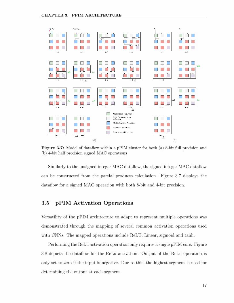
Figure 3.7: Model of dataflow within a pPIM cluster for both (a) 8-bit full precision and(b) 4-bit half precision signed MAC operations
Similarly to the unsigned integer MAC dataflow, the signed integer MAC dataflow
can be constructed from the partial products calculation. Figure 3.7 displays the
dataflow for a signed MAC operation with both 8-bit and 4-bit precision.
3.5 pPIM Activation Operations
Versatility of the pPIM architecture to adapt to represent multiple operations was
demonstrated through the mapping of several common activation operations used
with CNNs. The mapped operations include ReLU, Linear, sigmoid and tanh.
Performing the ReLu activation operation only requires a single pPIM core. Figure
3.8 depicts the dataflow for the ReLu activation. Output of the ReLu operation is
only set to zero if the input is negative. Due to this, the highest segment is used for
determining the output at each segment.
17
CHAPTER 3. PPIM ARCHITECTURE
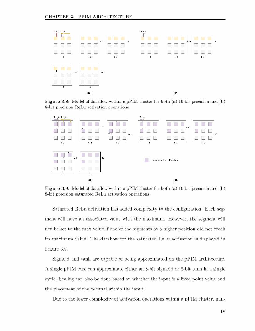
Figure 3.8: Model of dataflow within a pPIM cluster for both (a) 16-bit precision and (b)8-bit precision ReLu activation operations.
Figure 3.9: Model of dataflow within a pPIM cluster for both (a) 16-bit precision and (b)8-bit precision saturated ReLu activation operations.
Saturated ReLu activation has added complexity to the configuration. Each seg-
ment will have an associated value with the maximum. However, the segment will
not be set to the max value if one of the segments at a higher position did not reach
its maximum value. The dataflow for the saturated ReLu activation is displayed in
Figure 3.9.
Sigmoid and tanh are capable of being approximated on the pPIM architecture.
A single pPIM core can approximate either an 8-bit sigmoid or 8-bit tanh in a single
cycle. Scaling can also be done based on whether the input is a fixed point value and
the placement of the decimal within the input.
Due to the lower complexity of activation operations within a pPIM cluster, mul-
18

CHAPTER 3. PPIM ARCHITECTURE
Figure 3.10: Configuration of a pPIM cluster for quick switching between activationoperations.
tiple activation operations are capable of being configured into a single pPIM cluster.
This eliminates the process of reprogramming a cluster to perform a different acti-
vation operation. Figure 3.10 displays a pPIM cluster configured to perform ReLu,
saturated ReLu, sigmoid, and tanh activation operations.
a3
t=1 t=2 t=3
a2
t=4 t=5
a1
t=6 t=7 t=9
a0
t=10t=8
t=11 t=12 t=13 t=14
A0
Figure 3.11: Model of dataflow within a pPIM cluster for a 16-bit max-index operation.
Additionally, the index of a classification is capapble of being determined in the
pPIM cluster. The dataflow for this max-index operation is displayed in Figure 3.11.
The configuration consists of several pass cores, a comparison core, a conditional
core, and a counter core. Since only a single 4-bit segment of a cluster is capable of
19

CHAPTER 3. PPIM ARCHITECTURE
being compared at a time, each segment needs to be compared individually. These
comparisons begin with highest priority given to the most significant segment. If one
segment is greater than the other, the conditional core will prevent the input from
passing its value on to the following stages. Otherwise if the segments are equal, the
values will pass on and continue to be compared. In the final stage, the value of the
counter is passed on to the comparison core if the current operand is the new max
value. The comparison will then update the accumulator stored index if the index is
passed and vice versa.
3.6 FPGA Implementation
An FPGA implementation of the pPIM architecture is proposed for the validation.
Focus of the implemenation is on validating the processing elements and dataflow
through the simulation of unsigned 8-bit MAC operations on multiple pPIM clusters.
Classification is also handled by a pPIM cluster with a max-index dataflow. The final
implementation is used to predict numbers within images with a single layer NN.
3.6.1 Technology & Resources
Implementation of the pPIM architecture is run on the ZC702 base board. The
ZC702 base board delivers a package with both a programmable logic (PL) core and
processing system (PS). Implementation of the pPIM clusters is done solely on the
PL in a hardware descriptive language. Other features, such as communication with
the architecture are handled on the PS.
The dataset chosen for training and testing of the NN is the Modified Standards
and Technology (MNIST) dataset. Examples of images from the MNIST dataset
are displayed in Figure ??. Within the dataset is a compilation of 70,000 images
of handwritten digits, split into a training set of 60,000 images and testing set of
10,000 images. Images in the MNIST dataset are standardized to be in grayscale
20

CHAPTER 3. PPIM ARCHITECTURE
with dimensions of 28 pixels by 28 pixels.
Training of the NN is handled on Tensorflow before exporting into the FPGA
implementation. Tensorflow also provides access to the MNIST dataset for training
the model external to the ZC702 base board and testing the model on the board.
3.6.2 Machine Learning Model
The model trained for the validation of the pPIM architecture is a single layer NN.
The NN accepts input in the format of an imput vector of 784 pixels, each with an
8-bit unsigned integer value. The output of the model is a single numerical prediction
for the digit in the image, ranging from zero to nine.
The single NN layer within the model is a fully connected layer with no biases.
The output of the layer is a vector of ten 8-bit unsigned integers, the index of which
is relative to the digit that its prediction is associated with. The size of the weight
vector to handle an input with a size of 784 and output size of ten is a matrix with
the dimensions 10x784. Classification of the output vector is done with a max-index
operation where the index of the highest value prediction is the classification made
on the image.
3.6.3 pPIM Implementation
The FPGA implementation of the pPIM architecture is divided into two separate
regions: MAC operations and max-index operations. The FPGA implementation of
the two regions is depicted in Figure 3.12. A separate region is allocated to the two
operation types within the FPGA and neither is reconfigured. This is due to the
focus of the implementation on validating the way in which the pPIM architecture
processes data. Instead of requiring additional steps to handle the programming of
each cluster, constants are set into the pPIM cores’ register files.
To handle the dataflow and execution, each of the regions is coupled with a finite
21

CHAPTER 3. PPIM ARCHITECTURE
ControlSignals
MicrocodeTable
InputData
StartSignal
Fully Connected NNFSM
pPIM ClusterArrays
MAC Cluster RegionWeights
Block Memory
ImageData
DMA
ControlSignals
MicrocodeTable
InputData
StartSignal
Max-IndexFSM
Classification
pPIM ClusterArrays
Max Cluster Region
OutputVector
Figure 3.12: Structure of the multiple region approach to designing an FPGA implemen-tation of the pPIM architecture.
state machine. The The state machine is responsible for tracking input and output
to the region and beginning execution. When each cluster has its input ready, the
state machine sends a start signal to begin the execution. Once each of the inputs
have been processed, the state machine also sends the output to the next region or
memory.
3.6.4 Communication
Figure 3.13: Communication model between multiple elements within the ZC702 evalua-tion board and the host CPU.
Communication between the host computer and elements on the ZC702 base board
required the use of two communication protocols: direct memory access (DMA) and
universal asynchronous receiver-transmitter. The communication used between each
22
CHAPTER 3. PPIM ARCHITECTURE
of the elements in the implementation is shown in Figure 3.13.
The PS on the board provides hardware for UART communication. Over the
UART communication, the external host CPU is capable of communicating with the
PS. Over the UART communication the image data is passed from the host CPU to
the PS. The PS is also responsible for sending the image classification back to the
host CPU.
Both the PS and PL on the board are capable of DMA. DMA on the PL requires
introducing IP provided by Xilinx that communicates the data to the pPIM architec-
ture over an advanced extensible interface (AXI). Communication over DMA is used
to transfer the image data to the pPIM architecture and for the pPIM architecture
to return a classification on the image.
3.7 Results
3.7.1 pPIM Characteristics
Table 3.1: Synthesis results for pPIM architecture.
ComponentDelay(ns)
Power(mW)
Active Areaµm2
pPIM Core 0.8 2.7 4616.85pPIM Cluster
(MAC Operation)7.2 5.2 41551.66
The pPIM architecture is modelled in post-synthesis using the Synopsys Design
Compiler at a technology node of 28nm. Characteristics from the post-synthesis
model are recorded in Table 3.1. The model includes both a synthesized model of
the pPIM core and the pPIM cluster. Synthesis of the LUT multiplexers is modelled
using transmission gates, improving the area overhead of the design.
Gaining an accurate estimate of the activity of the pPIM cluster during operation
required having an example of the processing performed. An 8-bit unsigned MAC
23
CHAPTER 3. PPIM ARCHITECTURE
operation is chosen to record the power and delay figures for the pPIM cluster. This
gives an accurate estimation for analysis on deep learning models that contain MAC
operations for a majority of operations.
3.7.2 Performance Evalution
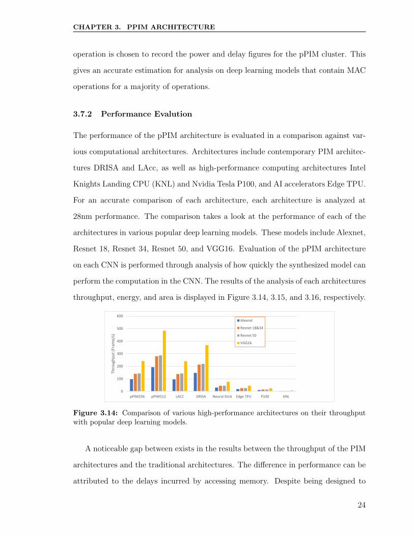
The performance of the pPIM architecture is evaluated in a comparison against var-
ious computational architectures. Architectures include contemporary PIM architec-
tures DRISA and LAcc, as well as high-performance computing architectures Intel
Knights Landing CPU (KNL) and Nvidia Tesla P100, and AI accelerators Edge TPU.
For an accurate comparison of each architecture, each architecture is analyzed at
28nm performance. The comparison takes a look at the performance of each of the
architectures in various popular deep learning models. These models include Alexnet,
Resnet 18, Resnet 34, Resnet 50, and VGG16. Evaluation of the pPIM architecture
on each CNN is performed through analysis of how quickly the synthesized model can
perform the computation in the CNN. The results of the analysis of each architectures
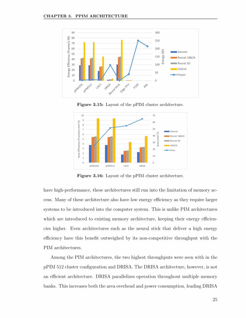
throughput, energy, and area is displayed in Figure 3.14, 3.15, and 3.16, respectively.
0
100
200
300
400
500
600
pPIM256 pPIM512 LACC DRISA Neural Stick Edge TPU P100 KNL
Thro
ugh
pu
t (F
ram
e/s)
Alexnet
Resnet 18&34
Resnet 50
VGG16
Figure 3.14: Comparison of various high-performance architectures on their throughputwith popular deep learning models.
A noticeable gap between exists in the results between the throughput of the PIM
architectures and the traditional architectures. The difference in performance can be
attributed to the delays incurred by accessing memory. Despite being designed to
24
CHAPTER 3. PPIM ARCHITECTURE
0
50
100
150
200
250
300
0
10
20
30
40
50
60
70
80
90
Ener
gy (
W)
Ener
gy E
ffic
ien
cy (
Fram
e/s-
W)
Alexnet
Resnet 18&34
Resnet 50
VGG16
Power
Figure 3.15: Layout of the pPIM cluster architecture.
0
10
20
30
40
50
60
70
0
1
2
3
4
5
6
7
8
9
10
pPIM256 pPIM512 LACC DRISA
Are
a (m
m^2
)
Are
a Ef
fici
ency
(Fr
ames
/s-m
m^2
)
Alexnet
Resnet 18&34
Resnet 50
VGG16
Area
Figure 3.16: Layout of the pPIM cluster architecture.
have high-performance, these architectures still run into the limitation of memory ac-
cess. Many of these architecture also have low energy efficiency as they require larger
systems to be introduced into the computer system. This is unlike PIM architectures
which are introduced to existing memory architecture, keeping their energy efficien-
cies higher. Even architectures such as the neural stick that deliver a high energy
efficiency have this benefit outweighed by its non-competitive throughput with the
PIM architectures.
Among the PIM architectures, the two highest throughputs were seen with in the
pPIM 512 cluster configuration and DRISA. The DRISA architecture, however, is not
an efficient architecture. DRISA parallelizes operation throughout multiple memory
banks. This increases both the area overhead and power consumption, leading DRISA
25
CHAPTER 3. PPIM ARCHITECTURE
to have the largest area and energy usage among each of the PIM architectures. The
pPIM 512 cluster configuration is able to provide a high throughput while maintaining
the highest area and energy efficiency among the PIM architectures, along with the
pPIM 256 cluster configuration. Even with a lower throughput than that of DRISA,
the pPIM 256 cluster configuration is able to outperform DRISA in terms of its
efficiency. LAcc is slightly more competitive in terms of efficiency than DRISA.
Despite this, the pPIM architectures outperform LAcc in all areas. This can be
attributed to the storage of LUT data within the memory bank, increasing both the
area and power costs.
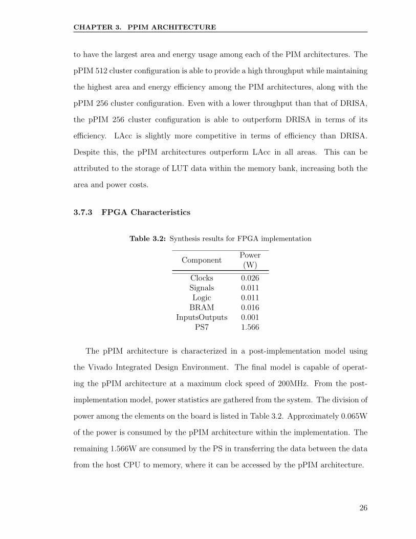
3.7.3 FPGA Characteristics
Table 3.2: Synthesis results for FPGA implementation
ComponentPower(W)
Clocks 0.026Signals 0.011Logic 0.011
BRAM 0.016InputsOutputs 0.001
PS7 1.566
The pPIM architecture is characterized in a post-implementation model using
the Vivado Integrated Design Environment. The final model is capable of operat-
ing the pPIM architecture at a maximum clock speed of 200MHz. From the post-
implementation model, power statistics are gathered from the system. The division of
power among the elements on the board is listed in Table 3.2. Approximately 0.065W
of the power is consumed by the pPIM architecture within the implementation. The
remaining 1.566W are consumed by the PS in transferring the data between the data
from the host CPU to memory, where it can be accessed by the pPIM architecture.
26
CHAPTER 3. PPIM ARCHITECTURE
3.7.4 FPGA Performance Evaluation
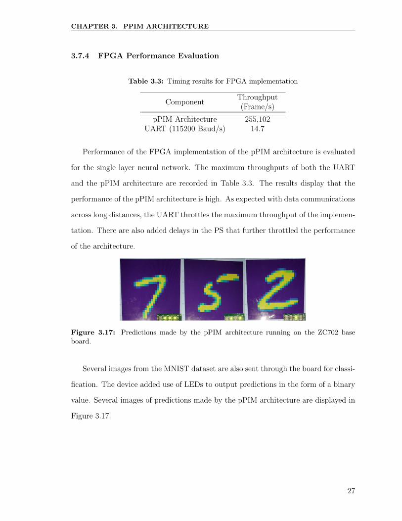
Table 3.3: Timing results for FPGA implementation
ComponentThroughput(Frame/s)
pPIM Architecture 255,102UART (115200 Baud/s) 14.7
Performance of the FPGA implementation of the pPIM architecture is evaluated
for the single layer neural network. The maximum throughputs of both the UART
and the pPIM architecture are recorded in Table 3.3. The results display that the
performance of the pPIM architecture is high. As expected with data communications
across long distances, the UART throttles the maximum throughput of the implemen-
tation. There are also added delays in the PS that further throttled the performance
of the architecture.
Figure 3.17: Predictions made by the pPIM architecture running on the ZC702 baseboard.
Several images from the MNIST dataset are also sent through the board for classi-
fication. The device added use of LEDs to output predictions in the form of a binary
value. Several images of predictions made by the pPIM architecture are displayed in
Figure 3.17.
27

Chapter 4
pPIM Instruction Set Architecture
Router
Accu
mul
ator
Cores
Rd. Buffer Wr. Buffer
Bitlines Memory Subarray
Row Buffer
Ctrl.Word
pPIMCluster
Addr. Ptr.Core Ptr.R/W Ptr.
Inst
r. R
egis
ter/
D
ecod
er
R
ow
Dec
oder
Microcode Table
Ctrl. Word 2Ctrl. Word 1
Ctrl. Word n
DRAM Addr. Bus
Program Counter
Hos
t CPU
Ctrl. Word 3
PIM Bank
Clk
Controller/Sequencer
Figure 4.1: Proposed ISA for handling control signals and memory accesses of the pPIMarchitecture.
The proposed ISA is designed to drive the pPIM architecture in performing data-
intensive applications such as CNNs used in deep learning models. The design of the
proposed ISA is depicted in Figure 4.1. The envisioned ISA is designed to not be lim-
ited to a set number of operations. Instead, the ISA is capable of being reprogrammed
to handle any operation with a dataflow mapped onto the pPIM cluster. This is ac-
complished through a micro-coded approach that allows for operation specific control
signalling. The instruction received by the ISA handles the three non-operation spe-
cific tasks: i) calling on operation specific control signalling, ii) reprogramming pPIM
cores register files, and iii) memory access by the pPIM clusters.
28
CHAPTER 4. PPIM INSTRUCTION SET ARCHITECTURE
4.1 ISA Communication
Cluster 1
Cluster 2
Cluster 8
Cluster 1
Cluster 16
SA 1
SA2
Memory Bank
Memory Controller
ISA Unit 1
Cluster 9
Cluster 10
Inst
ruct
ions
HOST CPU
Mem
ory
Acce
sses
ProcessThread 1
ISA Unit 2
ProcessThread 2
ProcessThread 8
Figure 4.2: Model of interface between the ISA with pPIM Clusters and memory elements.
The ISA is in communication with several elements internal and external to the
memory. These elements are the pPIM clusters, memory controller, memory subarray,
and the host CPU. This communication is outlined by Figure 4.2.
An ISA can control up to eight pPIM clusters within a ’column’ in unison. Any
action that the ISA performs on a pPIM cluster is also performed on the other pPIM
clusters within the pPIM column. This allows the ISA to operate with a higher degree
of parallelism while also limiting the overhead introduced into the pPIM architecture.
Communication between the host CPU and the ISA is limited to instructions sent
throught the memory controller. There is no transfer of data from the ISA back to
the host CPU as this is already accomplished by the memory controller. Adding data
transfer between the ISA and host CPU would only add unnecessary complexity to
the design.
4.2 pPIM Microcode
The ISA handles the large number of control signals within the pPIM cluster through
the use of micro-coded control words. The micro-coded control words add to the
reprogrammability of the pPIM architecture by avoiding operation specific hardware
29
CHAPTER 4. PPIM INSTRUCTION SET ARCHITECTURE
Halt
A Routing
B Routing
A Enable
B Enable
Output Routing
Reg Routing
Reg Enable
127
64
63 0
Figure 4.3: ISA
to determine control signals. Control words can easily be programmed into the mi-
crocode memory to suit a specific operation.
The microcode used by the pPIM architecture is stored into an SRAM memory
table, referred to as the microcode table. Within the microcode table is a 2-D array
of micro-coded control words that determine control signals sent to a pPIM column
for a single cycle. Within the memory, each of the control words are grouped into a
microcode sequence. This is a grouping of control words for a single operation ordered
sequentially in order of execution.
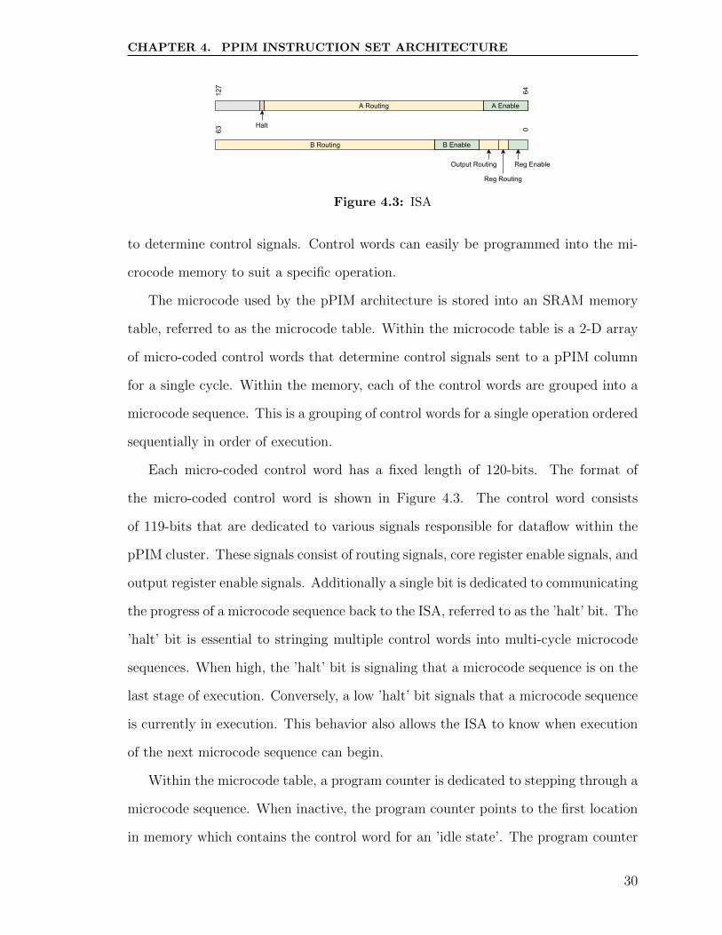
Each micro-coded control word has a fixed length of 120-bits. The format of
the micro-coded control word is shown in Figure 4.3. The control word consists
of 119-bits that are dedicated to various signals responsible for dataflow within the
pPIM cluster. These signals consist of routing signals, core register enable signals, and
output register enable signals. Additionally a single bit is dedicated to communicating
the progress of a microcode sequence back to the ISA, referred to as the ’halt’ bit. The
’halt’ bit is essential to stringing multiple control words into multi-cycle microcode
sequences. When high, the ’halt’ bit is signaling that a microcode sequence is on the
last stage of execution. Conversely, a low ’halt’ bit signals that a microcode sequence
is currently in execution. This behavior also allows the ISA to know when execution
of the next microcode sequence can begin.
Within the microcode table, a program counter is dedicated to stepping through a
microcode sequence. When inactive, the program counter points to the first location
in memory which contains the control word for an ’idle state’. The program counter
30
CHAPTER 4. PPIM INSTRUCTION SET ARCHITECTURE
continues to point at this ’idle state’ control word until directed to a microcode se-
quence by the ISA. Once directed to the address of a microcode sequence the program
counter iterates through each stage sequentially, cycle-by-cycle. This process contin-
ues until the program counter reaches a control word with a high ’halt’ bit. The ’halt’
bit results in the program counter returning to the ’idle state’ to await the ISA to
point to the next microcode sequence.
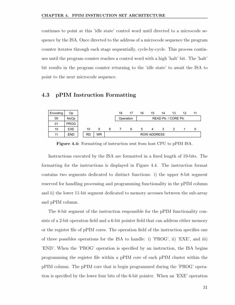
4.3 pPIM Instruction Formatting
Operation READ Ptr. / CORE Ptr.
RD WR ROW ADDRESS012345678910
111213141516171800011011
Encoding OpNoOpPROGEXEEND
Figure 4.4: Formatting of instruction sent from host CPU to pPIM ISA.
Instructions executed by the ISA are formatted in a fixed length of 19-bits. The
formatting for the instructions is displayed in Figure 4.4. The instruction format
contains two segments dedicated to distinct functions: i) the upper 8-bit segment
reserved for handling processing and programming functionality in the pPIM column
and ii) the lower 11-bit segment dedicated to memory accesses between the sub-array
and pPIM column.
The 8-bit segment of the instruction responsible for the pPIM functionality con-
sists of a 2-bit operation field and a 6-bit pointer field that can address either memory
or the register file of pPIM cores. The operation field of the instruction specifies one
of three possibles operations for the ISA to handle: i) ’PROG’, ii) ’EXE’, and iii)
’END’. When the ’PROG’ operation is specified by an instruction, the ISA begins
programming the register file within a pPIM core of each pPIM cluster within the
pPIM column. The pPIM core that is begin programmed during the ’PROG’ opera-
tion is specified by the lower four bits of the 6-bit pointer. When an ’EXE’ operation
31
CHAPTER 4. PPIM INSTRUCTION SET ARCHITECTURE
is specified, the ISA begins execution of microcode sequence within the pPIM column.
The starting address of the microcode sequence to be executed is specified by the 6-bit
pointer. At the end of a stream of executions, the ’END’ operation is sent to the ISA.
When the ’END’ operation is received, the ISA resets the core. This process includes
dumping the output registers of each pPIM cluster to the write buffers, followed by
resetting each of the registers. Doing so prepares the pPIM column to receive another
stream of instructions. An additional ’NoOp’ option is available for selection in the
operation field that performs no operation. This is used when only a memory access
necessary.
The 11-bit segment of the instruction dedicated to memory accesses between the
pPIM clusters and the sub-array consists of a write bit, read bit, and 9-bit row address
pointer. The 9-bit pointer gives the ISA the capability of addressing up to 512 memory
rows within the sub-array. When the read bit is set high, starting at the specified row
address, a byte for each of the pPIM clusters will be written from memory into the
read buffers for use in processing. Conversely, if the write bit is set high each cluster
will write their output register into the write buffers to be written sequentially into
the sub-array at the pointer address. If the write buffers are empty when a request is
made, the ISA will force the pPIM clusters to dump their output register data into
the write buffer without resetting the clusters. In the event that both the write and
read bit are set high, each memory access request is handled individually. First, the
ISA will handled the read request. Once the data is stored into the read buffers, the
ISA will proceed to handle the write request.
4.4 pPIM ISA Operation Mapping
The proposed ISA is capable of instructing a pPIM column to perform any pPIM
compatible operation. As a demonstration of the process of mapping an instruction
to the ISA, the unsigned 8-bit MAC dataflow from Figure 3.5a is mapped onto the
32
CHAPTER 4. PPIM INSTRUCTION SET ARCHITECTURE
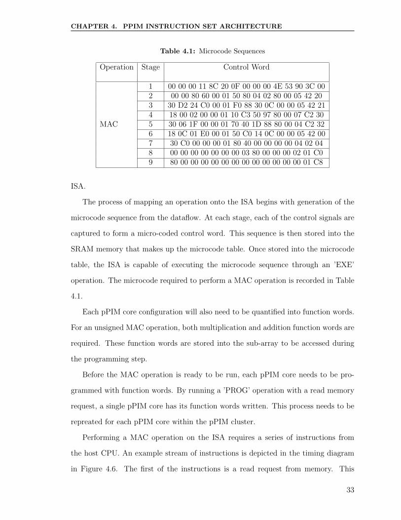
Table 4.1: Microcode Sequences
Operation Stage Control Word
1 00 00 00 11 8C 20 0F 00 00 00 4E 53 90 3C 002 00 00 80 60 00 01 50 80 04 02 80 00 05 42 203 30 D2 24 C0 00 01 F0 88 30 0C 00 00 05 42 214 18 00 02 00 00 01 10 C3 50 97 80 00 07 C2 30
MAC 5 30 06 1F 00 00 01 70 40 1D 88 80 00 04 C2 326 18 0C 01 E0 00 01 50 C0 14 0C 00 00 05 42 007 30 C0 00 00 00 01 80 40 00 00 00 00 04 02 048 00 00 00 00 00 00 00 03 80 00 00 00 02 01 C09 80 00 00 00 00 00 00 00 00 00 00 00 00 01 C8
ISA.
The process of mapping an operation onto the ISA begins with generation of the
microcode sequence from the dataflow. At each stage, each of the control signals are
captured to form a micro-coded control word. This sequence is then stored into the
SRAM memory that makes up the microcode table. Once stored into the microcode
table, the ISA is capable of executing the microcode sequence through an ’EXE’
operation. The microcode required to perform a MAC operation is recorded in Table
4.1.
Each pPIM core configuration will also need to be quantified into function words.
For an unsigned MAC operation, both multiplication and addition function words are
required. These function words are stored into the sub-array to be accessed during
the programming step.
Before the MAC operation is ready to be run, each pPIM core needs to be pro-
grammed with function words. By running a ’PROG’ operation with a read memory
request, a single pPIM core has its function words written. This process needs to be
repreated for each pPIM core within the pPIM cluster.
Performing a MAC operation on the ISA requires a series of instructions from
the host CPU. An example stream of instructions is depicted in the timing diagram
in Figure 4.6. The first of the instructions is a read request from memory. This
33

CHAPTER 4. PPIM INSTRUCTION SET ARCHITECTURE
MAC Operation Timing
RD MEM +MAC 1x8
MemoryOperation
MicrocodeOperation
ISAOperation
END+WRMEM
RD A[0:7]
RD B[0:7]
RD A[8:15]
RD B[8:15]
MAC[0]
MAC[1]
MAC[2]
MAC[3]
MAC[4]
MAC[5]
MAC[6]
MAC[7]
MAC[8]
MemoryOperation
MicrocodeOperation
ISAOperation
MAC[0]
MAC[1]
MAC[2]
MAC[3]
MAC[4]
MAC[5]
MAC[6]
MAC[7]
MAC[8]
WR Y[0:7]
RD MEM +MAC 1x8
Figure 4.5: Timing example of two consecutive MAC operations performed on a pPIMcluster by the pPIM ISA.
reads the operands for the MAC operation into the read buffers of each pPIM cluster.
Once the data becomes abailable to the pPIM column, an ’EXE’ instruction with
the starting address of the MAC operation is sent to the ISA. The process of reading
memory and executing MAC operations can be repeated as many times as needed
to accumulate over multiple calculations. Once execution of the MAC operations
complete, an ’END’ operation stores the output into the write buffers and resets the
pPIM column. Output is then stored into memory with a write request to memory.
4.5 FPGA Implementation
The FPGA implementation described in Section3.6 is further developed on in an
implementation that accepts instructions in the format outlined in Section 4.3. Im-
plementation of the pPIM ISA is used to demonstrate the ability of the ISA to perform
MAC operations.
4.5.1 Technology & Resources
Implementation of the pPIM ISA is run on the Pynq-Z1 board. The board delivers
a package from the same family as the ZC702 board. Additionally, the board had
34
CHAPTER 4. PPIM INSTRUCTION SET ARCHITECTURE
several PMOD ports available. This allowed the use of a PMOD compatible UART
component for communication with the board. The PL is then capable of direct
communication with the computer without the need for the UART and DMA of the
PS.
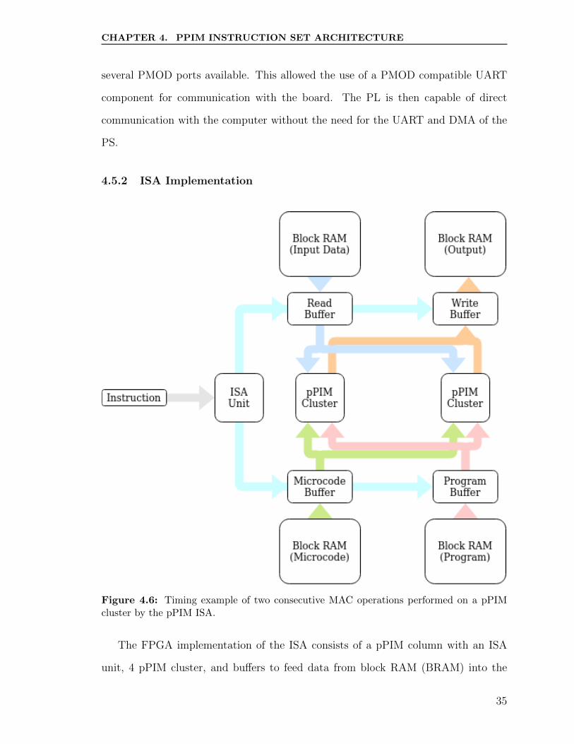
4.5.2 ISA Implementation
Figure 4.6: Timing example of two consecutive MAC operations performed on a pPIMcluster by the pPIM ISA.
The FPGA implementation of the ISA consists of a pPIM column with an ISA
unit, 4 pPIM cluster, and buffers to feed data from block RAM (BRAM) into the
35
CHAPTER 4. PPIM INSTRUCTION SET ARCHITECTURE
pPIM clusters. The structure of the FPGA implementation is outlined in Figure ??.
The implementation demonstrates all of the capabilities delivered by both the pPIM
architecture and the ISA. This includes executing microcode, programming the pPIM
cores, and making memory accesses.
Each BRAM element in the FPGA implementation is attached to the pPIM archi-
tecture with a buffer element. In the design these buffers are responsible for both pass-
ing data to the pPIM clusters and communicating contol information with the ISA.
Control information includes addresses, requests for memory accesses, and whether
the buffer is actively performing a memory access.
4.6 Results
4.6.1 ISA Characteristics
Table 4.2: Synthesis results for pPIM architecture with ISA.
ComponentDelay(ns)
Power(mW)
Active Areaµm2
PIM ISA 0.549 0.155 968.16PIM Column
(MAC Operation)7.2 43.355 333381.44
The proposed ISA is characterized with a post-synthesis model using the Synop-
sys Design Compiler at 28nm to match the process used to characterize the pPIM
architecture. The resulting characteristics produced by the post-synthesis model are
recorded in Table 4.2. The characterization creates a model of both the ISA individ-
ually and combines the ISA resultss with the pPIM clusters to characterize the pPIM
column.
Due to the ability of the ISA to parallelize operations within a column and perform
operations with the same dataflow, the number of cycles spent on an operation within
a pPIM cluster is unaffected by the ISA. The ISA also has a smaller delay than that of
36
CHAPTER 4. PPIM INSTRUCTION SET ARCHITECTURE
the pPIM clusters. With the proposed ISA the pPIM clusters are capable of operating
at its fastest possible clock speed. This allowed the impact on throughput within the
pPIM column to be minimized.
The added area overhead has a negligible effect on the overall pPIM architecture.
This is due to the small percentage of the pPIM column that is allocted for the ISA.
Approximately 0.0029% of the pPIM architecture’s area is dedicated to the ISA.
0.00001 0.0001 0.001 0.01 0.1 1
Alexnet
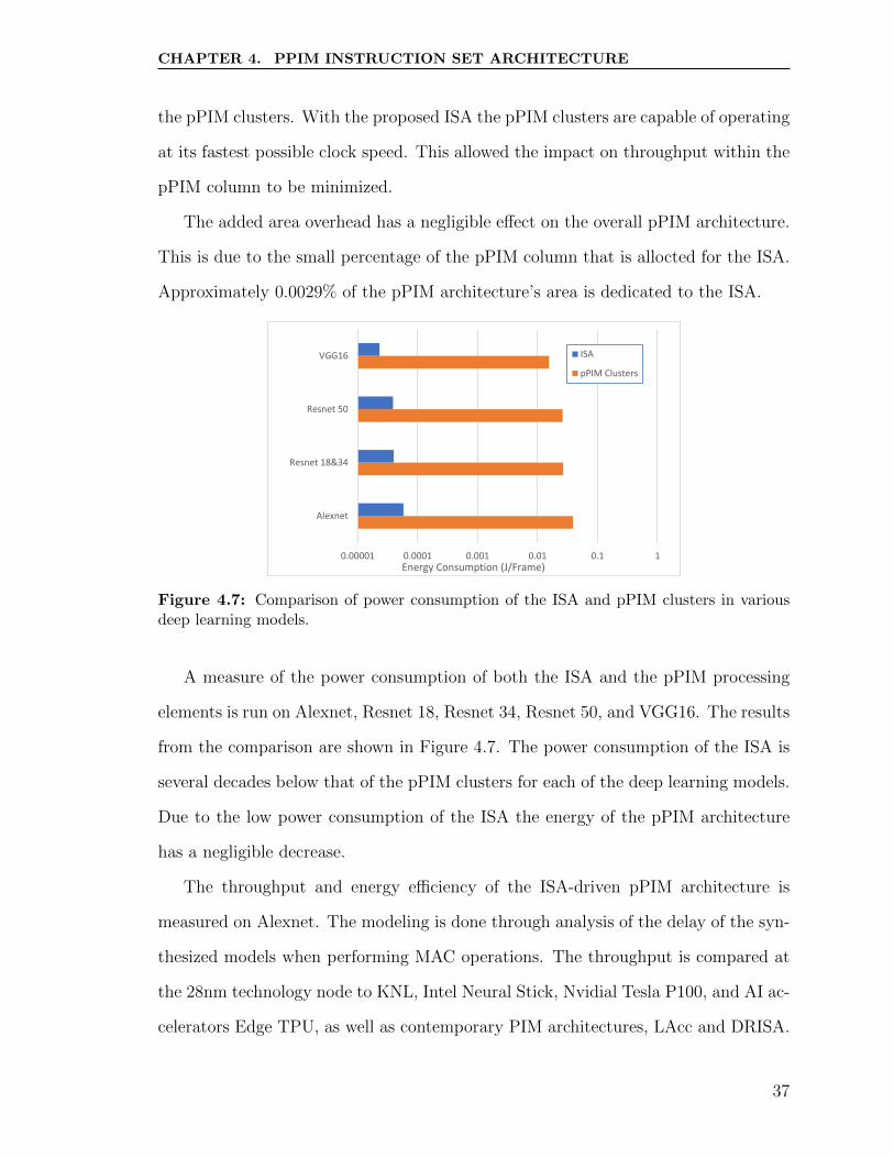
Resnet 18&34
Resnet 50
VGG16
Energy Consumption (J/Frame)
ISA
pPIM Clusters
Figure 4.7: Comparison of power consumption of the ISA and pPIM clusters in variousdeep learning models.
A measure of the power consumption of both the ISA and the pPIM processing
elements is run on Alexnet, Resnet 18, Resnet 34, Resnet 50, and VGG16. The results
from the comparison are shown in Figure 4.7. The power consumption of the ISA is
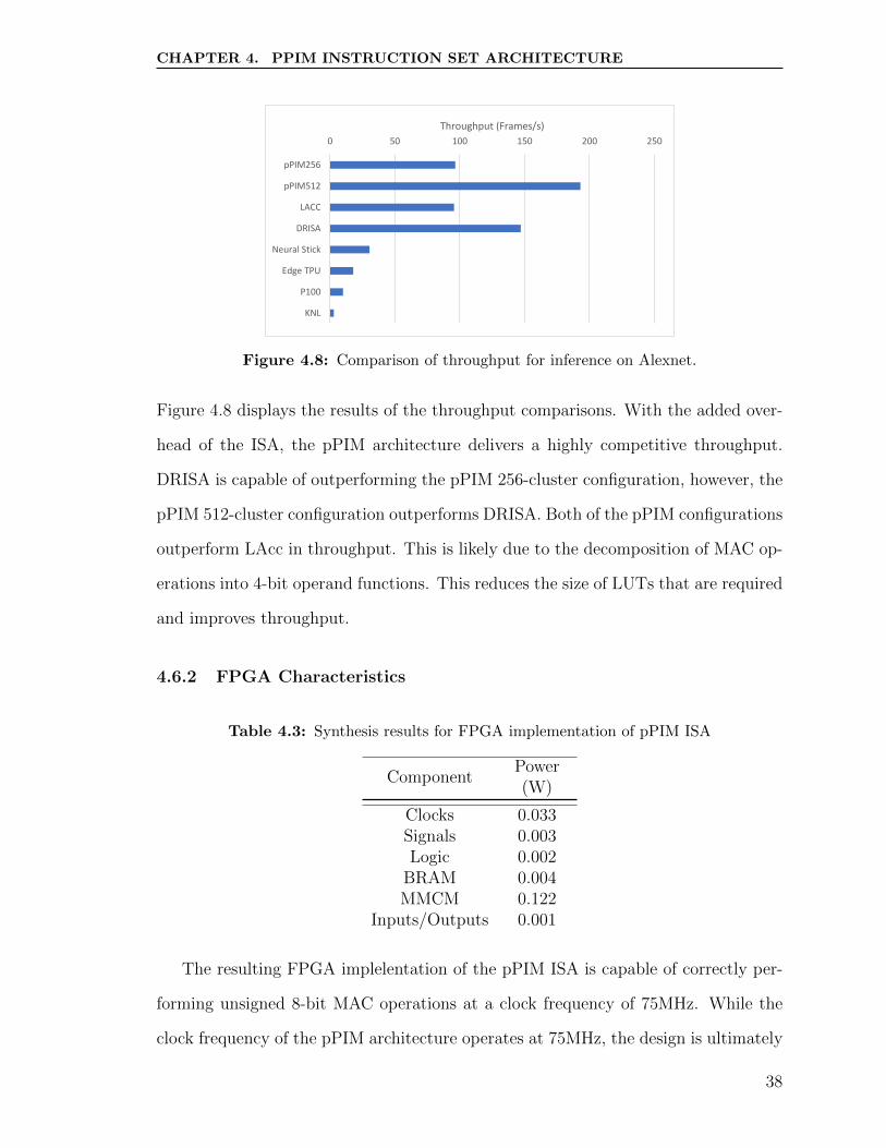
several decades below that of the pPIM clusters for each of the deep learning models.
Due to the low power consumption of the ISA the energy of the pPIM architecture
has a negligible decrease.
The throughput and energy efficiency of the ISA-driven pPIM architecture is
measured on Alexnet. The modeling is done through analysis of the delay of the syn-
thesized models when performing MAC operations. The throughput is compared at
the 28nm technology node to KNL, Intel Neural Stick, Nvidial Tesla P100, and AI ac-
celerators Edge TPU, as well as contemporary PIM architectures, LAcc and DRISA.
37
CHAPTER 4. PPIM INSTRUCTION SET ARCHITECTURE
0 50 100 150 200 250
pPIM256
pPIM512
LACC
DRISA
Neural Stick
Edge TPU
P100
KNL
Throughput (Frames/s)
Figure 4.8: Comparison of throughput for inference on Alexnet.
Figure 4.8 displays the results of the throughput comparisons. With the added over-
head of the ISA, the pPIM architecture delivers a highly competitive throughput.
DRISA is capable of outperforming the pPIM 256-cluster configuration, however, the
pPIM 512-cluster configuration outperforms DRISA. Both of the pPIM configurations
outperform LAcc in throughput. This is likely due to the decomposition of MAC op-
erations into 4-bit operand functions. This reduces the size of LUTs that are required
and improves throughput.
4.6.2 FPGA Characteristics
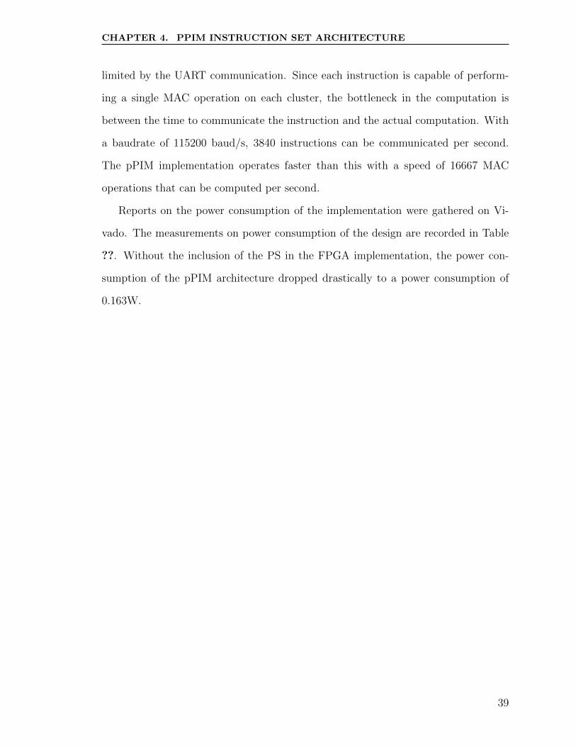
Table 4.3: Synthesis results for FPGA implementation of pPIM ISA
ComponentPower(W)
Clocks 0.033Signals 0.003Logic 0.002
BRAM 0.004MMCM 0.122
Inputs/Outputs 0.001
The resulting FPGA implelentation of the pPIM ISA is capable of correctly per-
forming unsigned 8-bit MAC operations at a clock frequency of 75MHz. While the
clock frequency of the pPIM architecture operates at 75MHz, the design is ultimately
38
CHAPTER 4. PPIM INSTRUCTION SET ARCHITECTURE
limited by the UART communication. Since each instruction is capable of perform-
ing a single MAC operation on each cluster, the bottleneck in the computation is
between the time to communicate the instruction and the actual computation. With
a baudrate of 115200 baud/s, 3840 instructions can be communicated per second.
The pPIM implementation operates faster than this with a speed of 16667 MAC
operations that can be computed per second.
Reports on the power consumption of the implementation were gathered on Vi-
vado. The measurements on power consumption of the design are recorded in Table
??. Without the inclusion of the PS in the FPGA implementation, the power con-
sumption of the pPIM architecture dropped drastically to a power consumption of
0.163W.
39
Chapter 5
Conclusions & Future Work
The growing divide between processing and memory architecture is driving the need
for high-performance architectures that reduce the penalties incurred by memory ac-
cess. Processing-in-memory (PIM) architectures take a step away from traditional
computer architectures by adding processing elements into memory and reducing the
memory access. The programmable PIM architecture delivers high-performance pro-
cessing while remaining reprogrammable to adapt to various applications. This is
accomplished through the use of LUT-based multiplexers that are capable of being
programmed to suit various functions and larger operations when processing in uni-
son. Compared to contemporary PIM architectures, the pPIM delivers competitive
throughputs with the highest level of efficiency for area and power consumptions.
An Instruction ISA is proposed for enabling the processing of data-intensive ap-
plications on the pPIM architecture. Through the use of a micro-coded approach
to handling the control signals of the pPIM architecture, the ISA is capable of ex-
ecuting any operation that is compatible with the pPIM architecture. The ISA is
capable running without hindering the performance of the pPIM architecture, with
low impact on the area overhead and power consumption.
Additionally a proof-of-concept, an FPGA model of the pPIM architecture is
designed for classification of images. The model implemented on the FPGA is a
single layer Neural Network (NN) that classified MINST images with a prediction of
40
CHAPTER 5. CONCLUSIONS & FUTURE WORK
the digit within the image. The implementation is capable of correctly classifying
images at a clock frequency of 200 MHz.
5.1 Future Work
The presented work delivers synthesized models for a PIM architecture and its ISA.
Additional steps are needed to further integration for programmers. These steps
include the development of a compiler and developing libraries that are capable of ex-
ecuting deep learning models on the pPIM architecture. The work also focuses on the
use of the pPIM architecture for deep learning applications. Further work is needed
to display the pPIM architecture’s ability to adapt to applications. This includes
developing applications such as encryption and encoding on the pPIM architecture.
The work presented on the proof-of-concept only tests the processing elements of
the pPIM architecture in a single layer NN. Research is needed into finding FPGAs
that will have a higher capacity to represent an entire 8-cluster pPIM column. The
pPIM architecture also needs to be proven to perform more complex machine learning
models. This requires that an FPGA implementation performs machine learning
models such as Alexnet and Resnet.
41
Bibliography
[1] S. McKee, “Reflections on the memory wall,” 2004.
[2] G. S. et al, “A review of near-memory computing architectures: Opportunitiesand challenges,” 2018.
[3] D. Patterson, “A case for intelligent ram,” 1997.
[4] M. Wulf and S. McKee, “Hitting the memory wall: Implications of the obvious,”1994.
[5] V. S. et al, “Rowclone: Fast and energy-efficientin-dram bulk data copy andinitialization,” 2013.
[6] ——, “Buddy-ram: Improving the performance and efficiency of bulk bitwiseoperations using dram,” 2016.
[7] ——, “Ambit: In-memory accelerator for bulk bitwise operationsusing commod-ity dram technology,” 2017.
[8] Q. D. et al, “Lacc: Exploiting lookup table-based fast and accurate vectormul-tiplication in dram-based cnn accelerator,” 2019.
[9] J. S. et al, “Lupis: Latch-up based ultra efficient processing in-memory system,”2018.
[10] S. Li, “Drisa: A dram-based reconfigurable in-situ accelerator,” 2017.
[11] Q. Deng, “Dracc: a dram based accelerator for accurate cnn inference,” 2018.
[12] P. C. et al, “Prime: A novel processing-in-memory architecture for neural net-work computation in reram-based main memory.”
[13] P. S. et al, “ppim: A programmable processor-in-memory architecture withprecision-scaling for deep learning,” 2020.
[14] A. Bear, “A novel processing-in-memory architecture for dense and sparse matrixmultiplications,” 2019.
[15] W. J. L. et al, “Design of processing-’inside’-memory optimized for dram behav-iors,” 2019.
[16] M. K. et al, “Software platform dedicated for in-memory computing circuit eval-uation,” 2020.
[17] ——, “Smart instruction codes for in-memory computing architectures compat-ible with standard sram interfaces,” 2018.
42
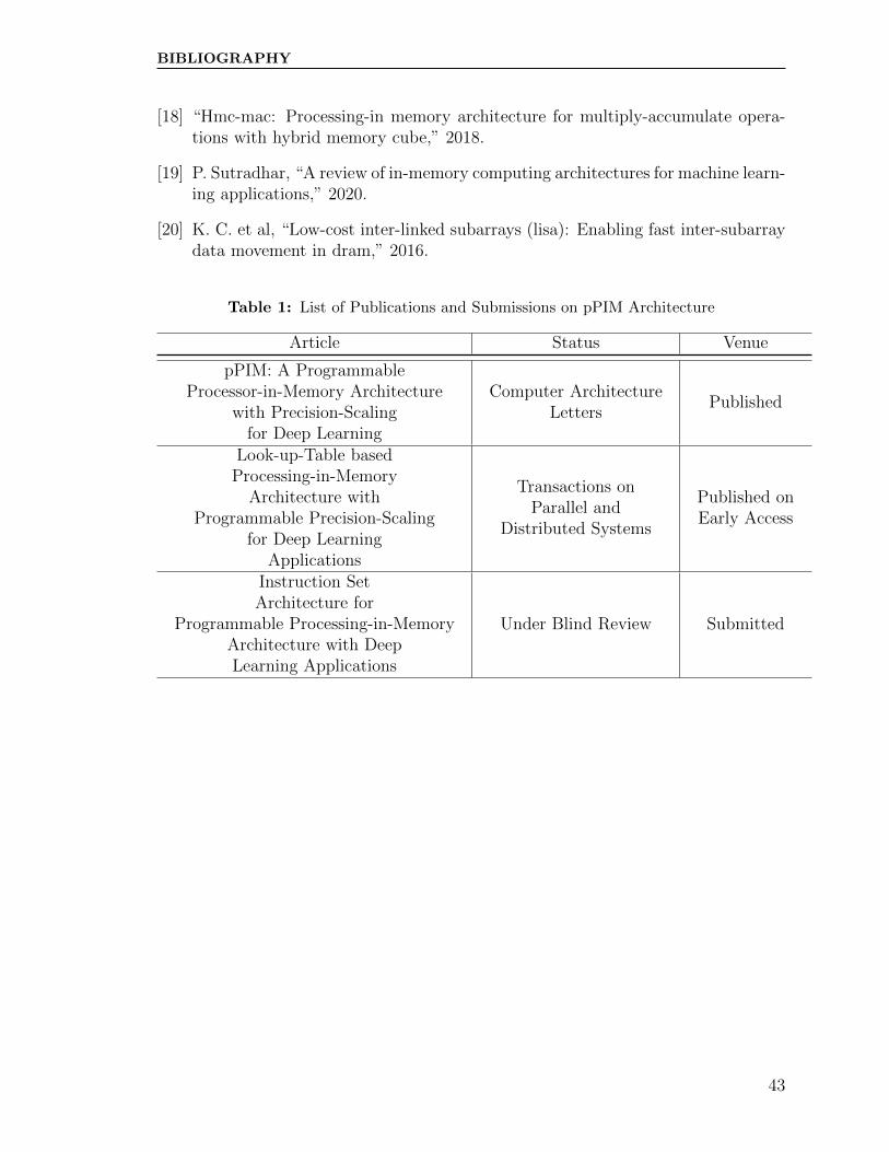
BIBLIOGRAPHY
[18] “Hmc-mac: Processing-in memory architecture for multiply-accumulate opera-tions with hybrid memory cube,” 2018.
[19] P. Sutradhar, “A review of in-memory computing architectures for machine learn-ing applications,” 2020.
[20] K. C. et al, “Low-cost inter-linked subarrays (lisa): Enabling fast inter-subarraydata movement in dram,” 2016.
Table 1: List of Publications and Submissions on pPIM Architecture
Article Status Venue
pPIM: A ProgrammableProcessor-in-Memory Architecture
with Precision-Scalingfor Deep Learning
Computer ArchitectureLetters
Published
Look-up-Table basedProcessing-in-Memory
Architecture withProgrammable Precision-Scaling
for Deep LearningApplications
Transactions onParallel and
Distributed Systems
Published onEarly Access
Instruction SetArchitecture for
Programmable Processing-in-MemoryArchitecture with DeepLearning Applications
Under Blind Review Submitted
43
Related Documents