1 7-1 Chapter 7 Memory and Programmable Logic 7-2 Outline ! Introduction ! Random-Access Memory ! Memory Decoding ! Error Detection and Correction ! Read-Only Memory ! Programmable Devices ! Sequential Programmable Devices

Welcome message from author
This document is posted to help you gain knowledge. Please leave a comment to let me know what you think about it! Share it to your friends and learn new things together.
Transcript
1
7-1
Chapter 7
Memory andProgrammable Logic
7-2
Outline
! Introduction! Random-Access Memory! Memory Decoding! Error Detection and Correction! Read-Only Memory! Programmable Devices! Sequential Programmable Devices
2
7-3
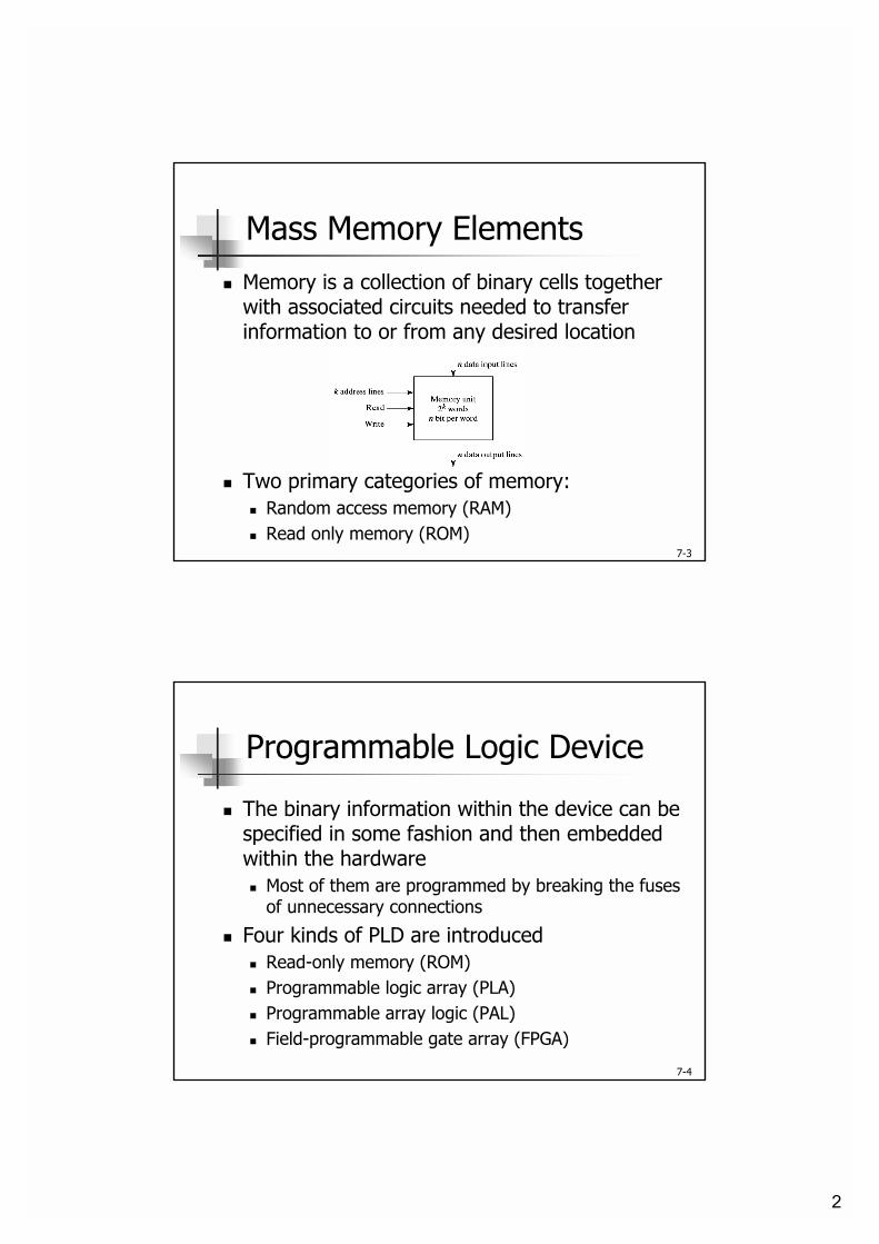
Mass Memory Elements! Memory is a collection of binary cells together
with associated circuits needed to transfer information to or from any desired location
! Two primary categories of memory:! Random access memory (RAM)! Read only memory (ROM)
7-4
Programmable Logic Device
! The binary information within the device can be specified in some fashion and then embedded within the hardware! Most of them are programmed by breaking the fuses
of unnecessary connections
! Four kinds of PLD are introduced! Read-only memory (ROM)! Programmable logic array (PLA)! Programmable array logic (PAL)! Field-programmable gate array (FPGA)
3
7-5
Outline
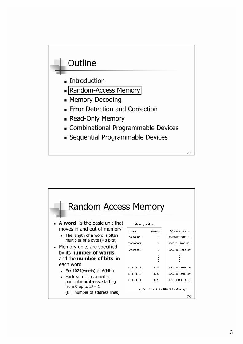
! Introduction! Random-Access Memory! Memory Decoding! Error Detection and Correction! Read-Only Memory! Combinational Programmable Devices! Sequential Programmable Devices
7-6
Random Access Memory
! A word is the basic unit that moves in and out of memory! The length of a word is often
multiples of a byte (=8 bits)
! Memory units are specified by its number of wordsand the number of bits in each word! Ex: 1024(words) x 16(bits)! Each word is assigned a
particular address, starting from 0 up to 2k � 1(k = number of address lines)
4
7-7
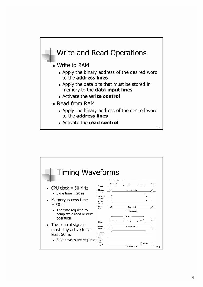
Write and Read Operations
! Write to RAM! Apply the binary address of the desired word
to the address lines! Apply the data bits that must be stored in
memory to the data input lines! Activate the write control
! Read from RAM! Apply the binary address of the desired word
to the address lines! Activate the read control
7-8
Timing Waveforms
! CPU clock = 50 MHz! cycle time = 20 ns
! Memory access time = 50 ns! The time required to
complete a read or write operation
! The control signals must stay active for at least 50 ns! 3 CPU cycles are required
5
7-9
Types of Memories! Access mode:
! Random access: any locations can be accessed in any order! Sequential access: accessed only when the requested word
has been reached (ex: hard disk)
! Operating mode:! Static RAM (SRAM)! Dynamic RAM (DRAM)
! Volatile mode:! Volatile memory: lose stored information when power is
turned off (ex: RAM)! Non-volatile memory: retain its storage after removal of
power (ex: flash, ROM, hard-disk, �)
7-10
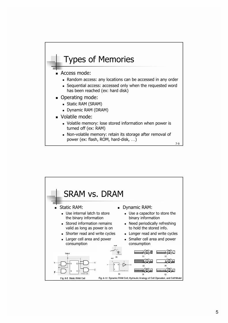
SRAM vs. DRAM! Static RAM:
! Use internal latch to store the binary information
! Stored information remains valid as long as power is on
! Shorter read and write cycles! Larger cell area and power
consumption
! Dynamic RAM:! Use a capacitor to store the
binary information! Need periodically refreshing
to hold the stored info.! Longer read and write cycles! Smaller cell area and power
consumption
6
7-11
Outline
! Introduction! Random-Access Memory! Memory Decoding! Error Detection and Correction! Read-Only Memory! Combinational Programmable Devices! Sequential Programmable Devices
7-12
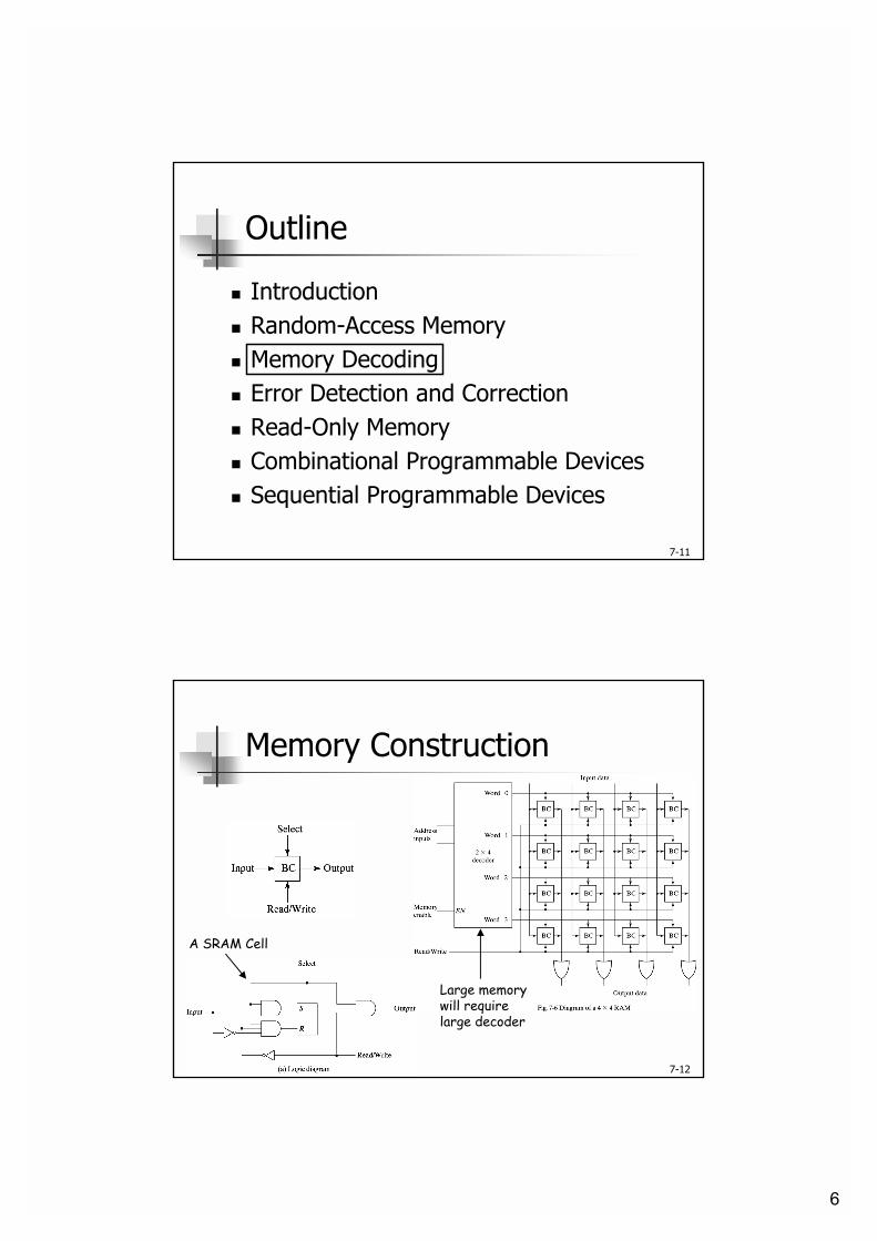
Memory Construction
A SRAM Cell
Large memorywill requirelarge decoder
7
7-13
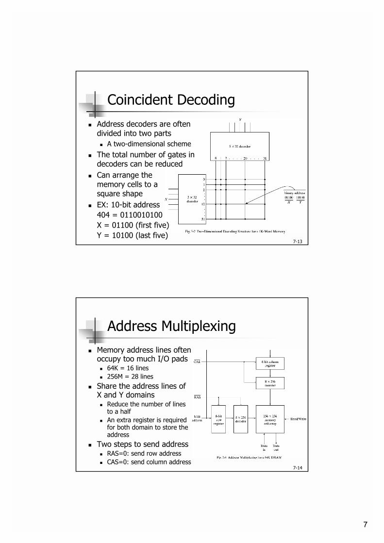
Coincident Decoding! Address decoders are often
divided into two parts! A two-dimensional scheme
! The total number of gates in decoders can be reduced
! Can arrange thememory cells to asquare shape
! EX: 10-bit address404 = 0110010100X = 01100 (first five)Y = 10100 (last five)
7-14
Address Multiplexing! Memory address lines often
occupy too much I/O pads! 64K = 16 lines! 256M = 28 lines
! Share the address lines of X and Y domains! Reduce the number of lines
to a half! An extra register is required
for both domain to store the address
! Two steps to send address! RAS=0: send row address! CAS=0: send column address
8
7-15
Outline
! Introduction! Random-Access Memory! Memory Decoding! Error Detection and Correction! Read-Only Memory! Combinational Programmable Devices! Sequential Programmable Devices
7-16
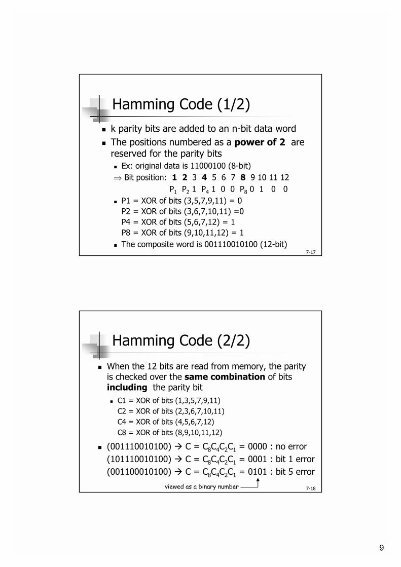
Error Detection & Correction! Memory arrays are often very huge
! May cause occasional errors in data access
! Reliability of memory can be improved by employing error-detecting and correcting codes
! Error-detecting code: only check for the existenceof errors! Most common scheme is the parity bit
! Error-correcting code: check the existence and locations of errors! Use multiple parity check bits to generate a syndrome
that can indicate the erroneous bits! Complement the erroneous bits can correct the errors
9
7-17
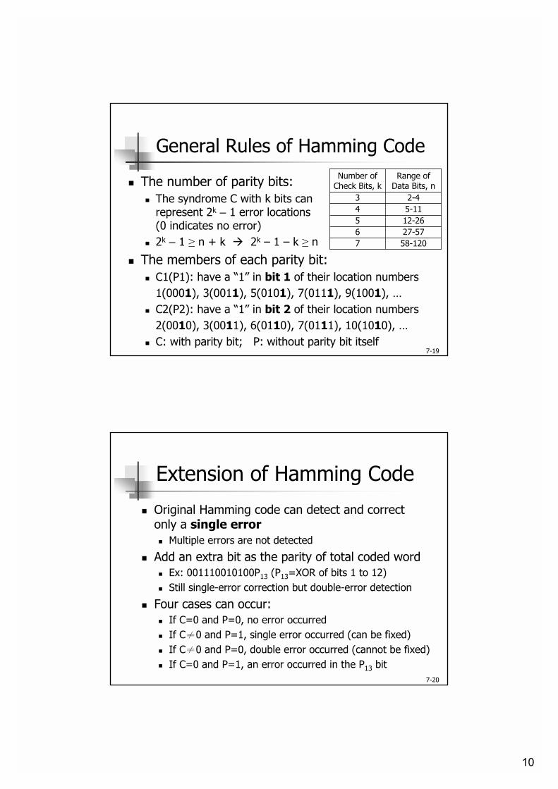
Hamming Code (1/2)! k parity bits are added to an n-bit data word! The positions numbered as a power of 2 are
reserved for the parity bits! Ex: original data is 11000100 (8-bit)⇒ Bit position: 1 2 3 4 5 6 7 8 9 10 11 12
P1 P2 1 P4 1 0 0 P8 0 1 0 0! P1 = XOR of bits (3,5,7,9,11) = 0
P2 = XOR of bits (3,6,7,10,11) =0P4 = XOR of bits (5,6,7,12) = 1P8 = XOR of bits (9,10,11,12) = 1
! The composite word is 001110010100 (12-bit)
7-18
Hamming Code (2/2)
! When the 12 bits are read from memory, the parity is checked over the same combination of bits including the parity bit! C1 = XOR of bits (1,3,5,7,9,11)
C2 = XOR of bits (2,3,6,7,10,11)C4 = XOR of bits (4,5,6,7,12)C8 = XOR of bits (8,9,10,11,12)
! (001110010100) " C = C8C4C2C1 = 0000 : no error(101110010100) " C = C8C4C2C1 = 0001 : bit 1 error(001100010100) " C = C8C4C2C1 = 0101 : bit 5 error
viewed as a binary number
10
7-19
General Rules of Hamming Code
! The number of parity bits:! The syndrome C with k bits can
represent 2k � 1 error locations(0 indicates no error)
! 2k � 1 ≥ n + k " 2k � 1 � k ≥ n
! The members of each parity bit:! C1(P1): have a �1� in bit 1 of their location numbers
1(0001), 3(0011), 5(0101), 7(0111), 9(1001), �! C2(P2): have a �1� in bit 2 of their location numbers
2(0010), 3(0011), 6(0110), 7(0111), 10(1010), �! C: with parity bit; P: without parity bit itself
58-120727-57612-2655-1142-43
Range of Data Bits, n
Number of Check Bits, k
7-20
Extension of Hamming Code
! Original Hamming code can detect and correct only a single error! Multiple errors are not detected
! Add an extra bit as the parity of total coded word! Ex: 001110010100P13 (P13=XOR of bits 1 to 12)! Still single-error correction but double-error detection
! Four cases can occur:! If C=0 and P=0, no error occurred! If C≠0 and P=1, single error occurred (can be fixed)! If C≠0 and P=0, double error occurred (cannot be fixed)! If C=0 and P=1, an error occurred in the P13 bit
11
7-21
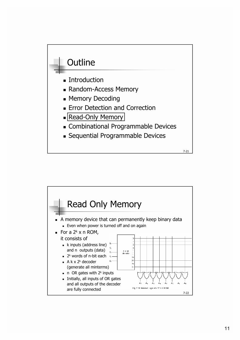
Outline
! Introduction! Random-Access Memory! Memory Decoding! Error Detection and Correction! Read-Only Memory! Combinational Programmable Devices! Sequential Programmable Devices
7-22
Read Only Memory! A memory device that can permanently keep binary data
! Even when power is turned off and on again
! For a 2k x n ROM,it consists of! k inputs (address line)
and n outputs (data)! 2k words of n-bit each! A k x 2k decoder
(generate all minterms)! n OR gates with 2k inputs! Initially, all inputs of OR gates
and all outputs of the decoderare fully connected
12
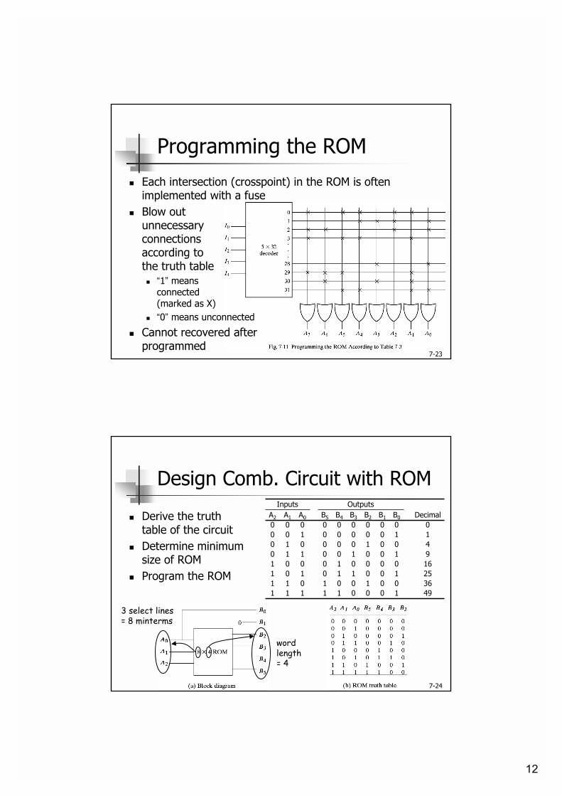
7-23
Programming the ROM! Each intersection (crosspoint) in the ROM is often
implemented with a fuse! Blow out
unnecessaryconnectionsaccording tothe truth table! �1� means
connected(marked as X)
! �0� means unconnected
! Cannot recovered afterprogrammed
7-24
Design Comb. Circuit with ROM
! Derive the truth table of the circuit
! Determine minimum size of ROM
! Program the ROM491000111113600100101125100110101160000100019100100110400100001011000001000000000000
DecimalB0B1B2B3B4B5A0A1A2
OutputsInputs
3 select lines= 8 minterms
wordlength= 4
13
7-25
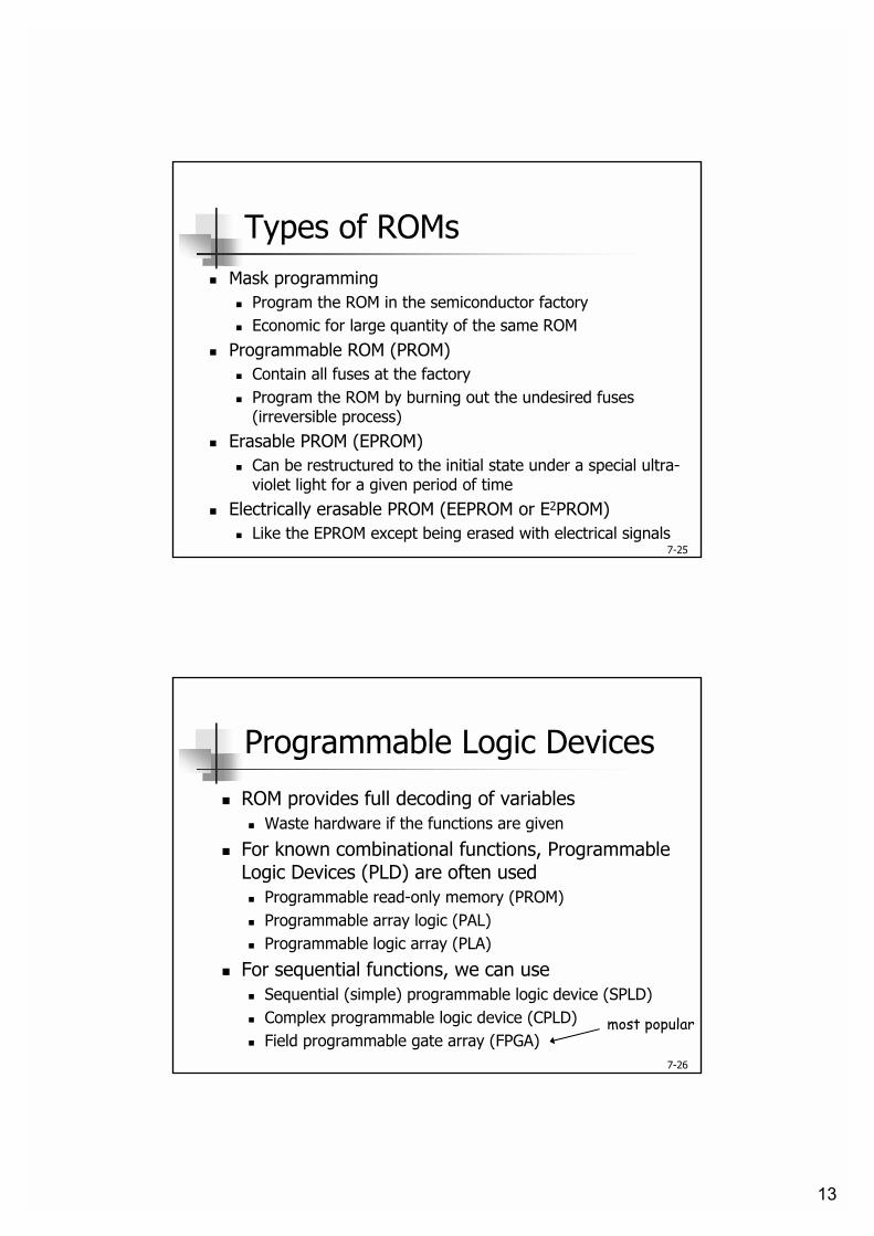
Types of ROMs! Mask programming
! Program the ROM in the semiconductor factory! Economic for large quantity of the same ROM
! Programmable ROM (PROM)! Contain all fuses at the factory! Program the ROM by burning out the undesired fuses
(irreversible process)! Erasable PROM (EPROM)
! Can be restructured to the initial state under a special ultra-violet light for a given period of time
! Electrically erasable PROM (EEPROM or E2PROM)! Like the EPROM except being erased with electrical signals
7-26
Programmable Logic Devices
! ROM provides full decoding of variables! Waste hardware if the functions are given
! For known combinational functions, Programmable Logic Devices (PLD) are often used! Programmable read-only memory (PROM)! Programmable array logic (PAL)! Programmable logic array (PLA)
! For sequential functions, we can use! Sequential (simple) programmable logic device (SPLD)! Complex programmable logic device (CPLD)! Field programmable gate array (FPGA)
most popular
14
7-27
Outline
! Introduction! Random-Access Memory! Memory Decoding! Error Detection and Correction! Read-Only Memory! Combinational Programmable Devices! Sequential Programmable Devices
7-28
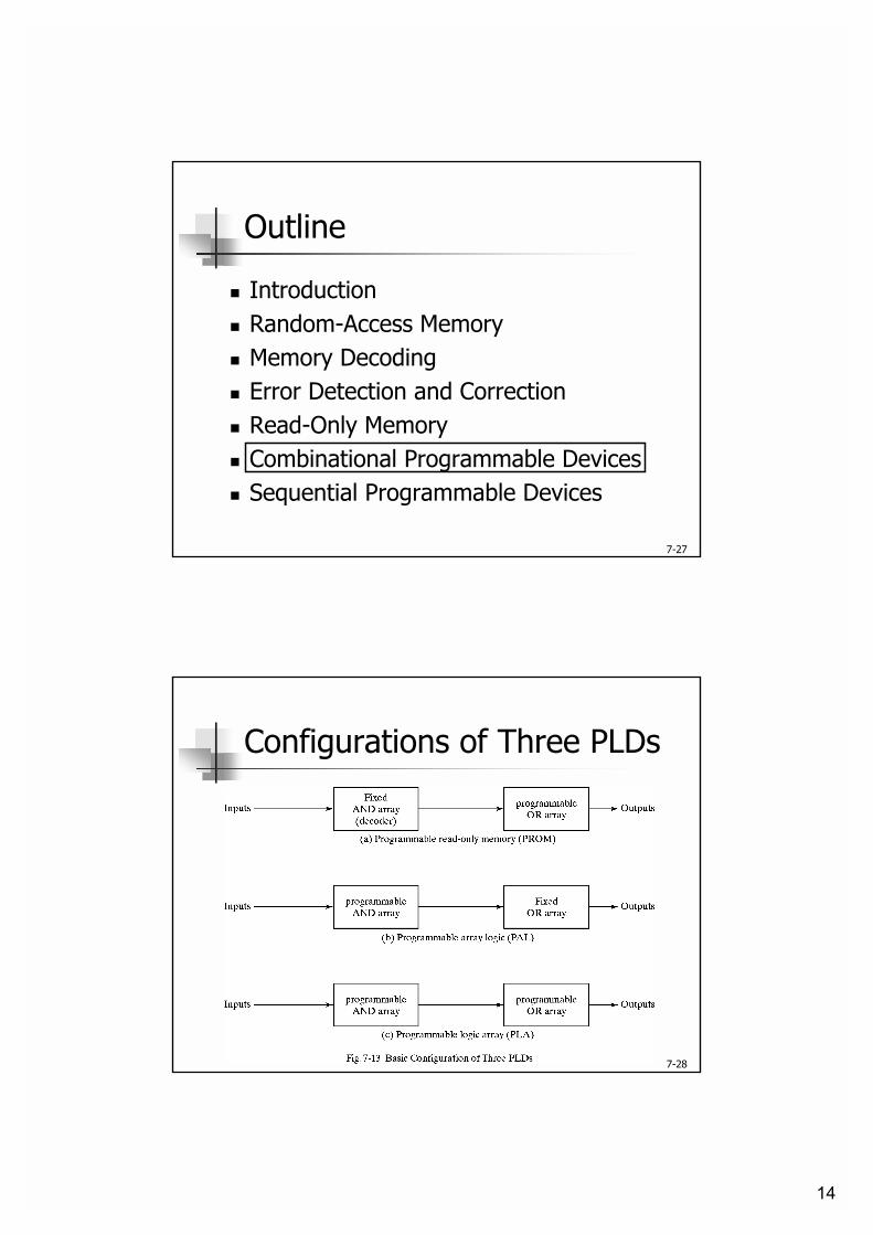
Configurations of Three PLDs
15
7-29
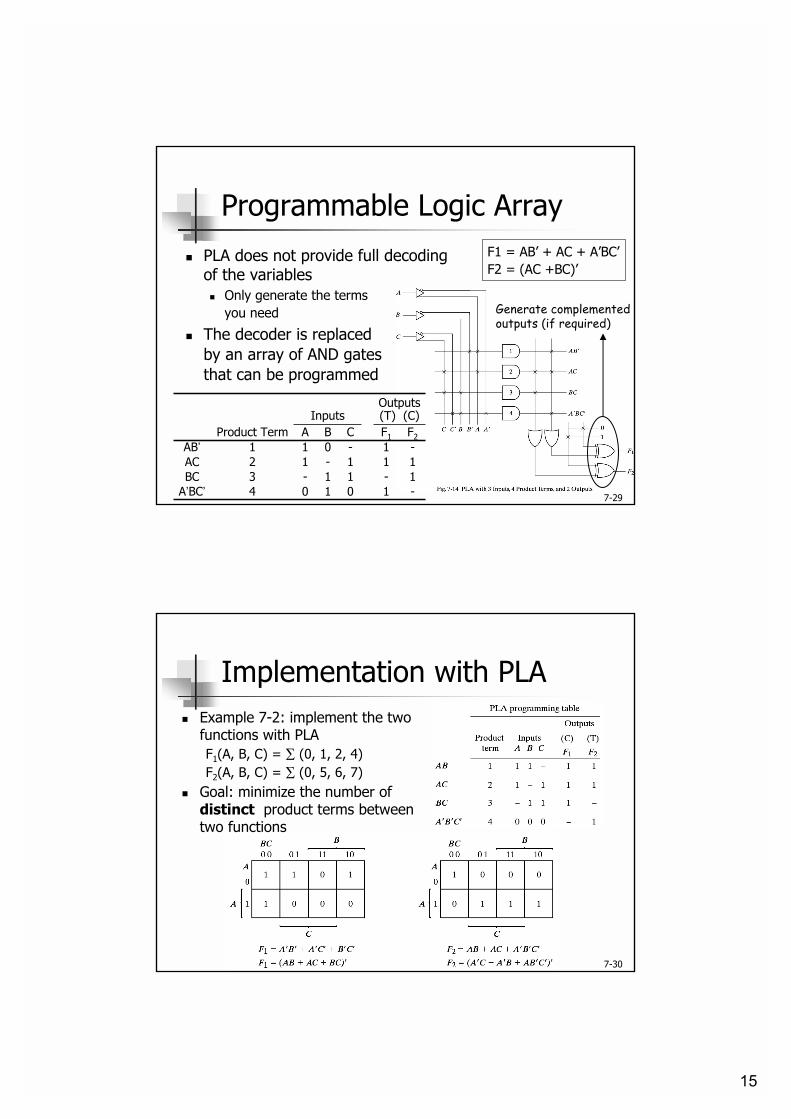
Programmable Logic Array! PLA does not provide full decoding
of the variables! Only generate the terms
you need
! The decoder is replacedby an array of AND gatesthat can be programmed
-10104A�BC�1-11-3BC111-12AC-1-011AB�F2F1CBAProduct Term
Outputs(T) (C)Inputs
Generate complementedoutputs (if required)
F1 = AB� + AC + A�BC�F2 = (AC +BC)�
7-30
Implementation with PLA! Example 7-2: implement the two
functions with PLAF1(A, B, C) = ∑ (0, 1, 2, 4)F2(A, B, C) = ∑ (0, 5, 6, 7)
! Goal: minimize the number of distinct product terms between two functions
16
7-31
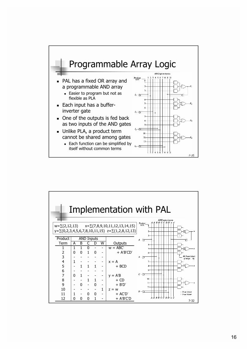
Programmable Array Logic
! PAL has a fixed OR array and a programmable AND array! Easier to program but not as
flexible as PLA
! Each input has a buffer-inverter gate
! One of the outputs is fed back as two inputs of the AND gates
! Unlike PLA, a product term cannot be shared among gates! Each function can be simplified by
itself without common terms
7-32
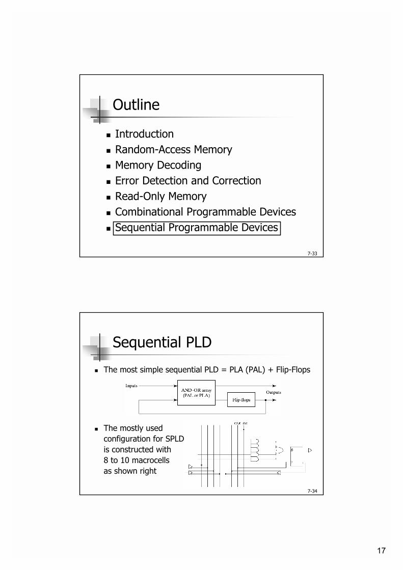
Implementation with PAL
+ A�B�C�D-100012+ AC�D�-00-111
z = w1----10+ B�D�-0-0-9+ CD-11--8
y = A�B---107-----6
+ BCD-111-5x = A----14
-----3+ A�B�CD�-01002
w = ABC�--0111OutputsWDCBATerm
AND InputsProduct
w=∑(2,12,13) x=∑(7,8,9,10,11,12,13,14,15)y=∑(0,2,3,4,5,6,7,8,10,11,15) z=∑(1,2,8,12,13)
17
7-33
Outline
! Introduction! Random-Access Memory! Memory Decoding! Error Detection and Correction! Read-Only Memory! Combinational Programmable Devices! Sequential Programmable Devices
7-34
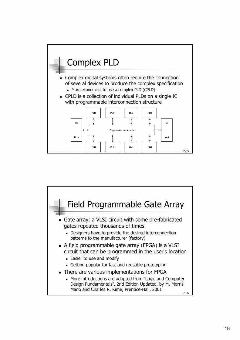
Sequential PLD
! The most simple sequential PLD = PLA (PAL) + Flip-Flops
! The mostly usedconfiguration for SPLDis constructed with8 to 10 macrocellsas shown right
18
7-35
Complex PLD! Complex digital systems often require the connection
of several devices to produce the complex specification! More economical to use a complex PLD (CPLD)
! CPLD is a collection of individual PLDs on a single IC with programmable interconnection structure
7-36
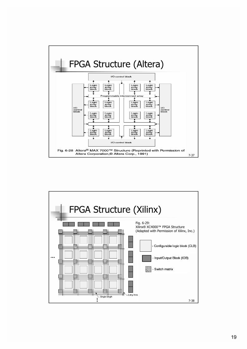
Field Programmable Gate Array
! Gate array: a VLSI circuit with some pre-fabricated gates repeated thousands of times! Designers have to provide the desired interconnection
patterns to the manufacturer (factory)
! A field programmable gate array (FPGA) is a VLSI circuit that can be programmed in the user�s location! Easier to use and modify! Getting popular for fast and reusable prototyping
! There are various implementations for FPGA! More introductions are adopted from �Logic and Computer
Design Fundamentals�, 2nd Edition Updated, by M. Morris Mano and Charles R. Kime, Prentice-Hall, 2001
19
7-37
FPGA Structure (Altera)
7-38
FPGA Structure (Xilinx)Fig. 6-29:Xilinx® XC4000� FPGA Structure(Adapted with Permission of Xilinx, Inc.)
20
7-39
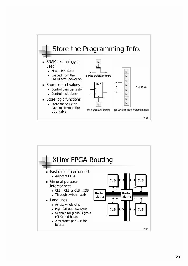
Store the Programming Info.
! SRAM technology is used! M = 1-bit SRAM! Loaded from the
PROM after power on
! Store control values! Control pass transistor! Control multiplexer
! Store logic functions! Store the value of
each minterm in the truth table
7-40
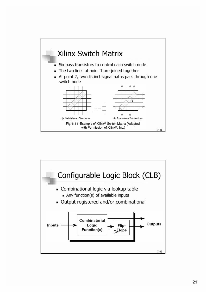
Xilinx FPGA Routing! Fast direct interconnect
! Adjacent CLBs
! General purpose interconnect! CLB � CLB or CLB � IOB! Through switch matrix
! Long lines! Across whole chip! High fan-out, low skew! Suitable for global signals
(CLK) and buses! 2 tri-states per CLB for
busses
21
7-41
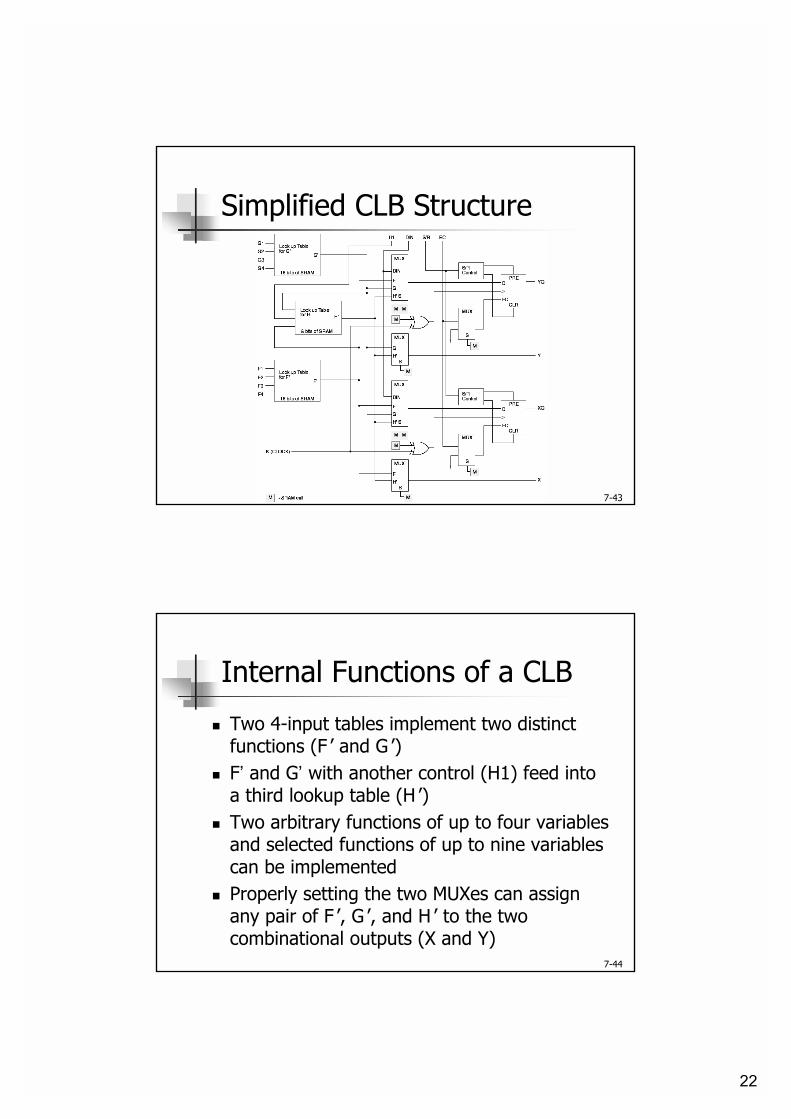
Xilinx Switch Matrix! Six pass transistors to control each switch node! The two lines at point 1 are joined together! At point 2, two distinct signal paths pass through one
switch node
7-42
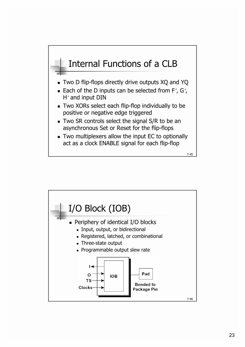
Configurable Logic Block (CLB)
! Combinational logic via lookup table! Any function(s) of available inputs
! Output registered and/or combinational
22
7-43
Simplified CLB Structure
7-44
Internal Functions of a CLB
! Two 4-input tables implement two distinct functions (F � and G �)
! F� and G� with another control (H1) feed into a third lookup table (H �)
! Two arbitrary functions of up to four variables and selected functions of up to nine variables can be implemented
! Properly setting the two MUXes can assign any pair of F �, G �, and H � to the two combinational outputs (X and Y)
23
7-45
Internal Functions of a CLB
! Two D flip-flops directly drive outputs XQ and YQ! Each of the D inputs can be selected from F �, G �,
H � and input DIN! Two XORs select each flip-flop individually to be
positive or negative edge triggered! Two SR controls select the signal S/R to be an
asynchronous Set or Reset for the flip-flops! Two multiplexers allow the input EC to optionally
act as a clock ENABLE signal for each flip-flop
7-46
I/O Block (IOB)! Periphery of identical I/O blocks
! Input, output, or bidirectional! Registered, latched, or combinational! Three-state output! Programmable output slew rate
24
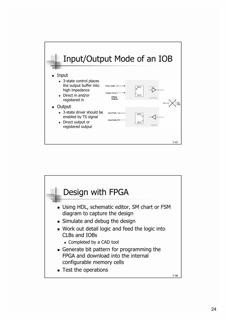
7-47
Input/Output Mode of an IOB
! Input! 3-state control places
the output buffer into high impedance
! Direct in and/or registered in
! Output! 3-state driver should be
enabled by TS signal! Direct output or
registered output
7-48
Design with FPGA
! Using HDL, schematic editor, SM chart or FSM diagram to capture the design
! Simulate and debug the design! Work out detail logic and feed the logic into
CLBs and IOBs! Completed by a CAD tool
! Generate bit pattern for programming the FPGA and download into the internal configurable memory cells
! Test the operations
25
7-49
FPGA Design Flow
! Advantages: Fast and reusable prototyping! Can be reprogrammed and reused! Implementation time is very short
! Disadvantages: Expensive and high volume
logic + layout synthesis
7-50
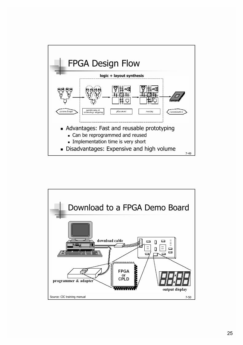
Download to a FPGA Demo Board
Source: CIC training manual
Related Documents