This document is downloaded from DR-NTU, Nanyang Technological University Library, Singapore. Title A power-delay efficient hybrid carry-lookahead/carry- select based redundant binary to two’s complement converter. Author(s) He, Yajuan.; Chang, Chip Hong. Citation He, Y., & Chang, C. H. (2008). A power-delay efficient hybrid carry-lookahead/carry-select based redundant binary to two’s complement converter. IEEE Transactions on Circuits and Systems Part 1 Regular Papers. 55(1), 336-346. Date 2008 URL http://hdl.handle.net/10220/6328 Rights © 2008 IEEE. Personal use of this material is permitted. However, permission to reprint/republish this material for advertising or promotional purposes or for creating new collective works for resale or redistribution to servers or lists, or to reuse any copyrighted component of this work in other works must be obtained from the IEEE. This material is presented to ensure timely dissemination of scholarly and technical work. Copyright and all rights therein are retained by authors or by other copyright holders. All persons copying this information are expected to adhere to the terms and constraints invoked by each author's copyright. In most cases, these works may not be reposted without the explicit permission of the copyright holder. http://www.ieee.org/portal/site This material is presented to ensure timely dissemination of scholarly and technical work. Copyright and all rights therein are retained by authors or by other copyright holders. All persons copying this information are expected to adhere to the terms and constraints invoked by each author's copyright. In most cases, these works may not be reposted without the explicit permission of the copyright holder.

Welcome message from author
This document is posted to help you gain knowledge. Please leave a comment to let me know what you think about it! Share it to your friends and learn new things together.
Transcript

This document is downloaded from DR-NTU, Nanyang Technological
University Library, Singapore.
TitleA power-delay efficient hybrid carry-lookahead/carry-select based redundant binary to two’s complementconverter.
Author(s) He, Yajuan.; Chang, Chip Hong.
Citation
He, Y., & Chang, C. H. (2008). A power-delay efficienthybrid carry-lookahead/carry-select based redundantbinary to two’s complement converter. IEEE Transactionson Circuits and Systems Part 1 Regular Papers. 55(1),336-346.
Date 2008
URL http://hdl.handle.net/10220/6328
Rights
© 2008 IEEE. Personal use of this material is permitted.However, permission to reprint/republish this material foradvertising or promotional purposes or for creating newcollective works for resale or redistribution to servers orlists, or to reuse any copyrighted component of this workin other works must be obtained from the IEEE. Thismaterial is presented to ensure timely dissemination ofscholarly and technical work. Copyright and all rightstherein are retained by authors or by other copyrightholders. All persons copying this information areexpected to adhere to the terms and constraints invokedby each author's copyright. In most cases, these worksmay not be reposted without the explicit permission of thecopyright holder. http://www.ieee.org/portal/site Thismaterial is presented to ensure timely dissemination ofscholarly and technical work. Copyright and all rightstherein are retained by authors or by other copyrightholders. All persons copying this information areexpected to adhere to the terms and constraints invokedby each author's copyright. In most cases, these worksmay not be reposted without the explicit permission of thecopyright holder.
336 IEEE TRANSACTIONS ON CIRCUITS AND SYSTEMS—I: REGULAR PAPERS, VOL. 55, NO. 1, FEBRUARY 2008
A Power-Delay Efficient HybridCarry-Lookahead/Carry-Select Based
Redundant Binary to Two’s Complement ConverterYajuan He, Student Member, IEEE, and Chip-Hong Chang, Senior Member, IEEE
Abstract—This paper presents an efficient reverse converter fortransforming the redundant binary (RB) representation into two’scomplement form. The hierarchical expansion of the carry equa-tion for the reverse conversion algorithm creates a regular multi-level structure, from which a high-speed hybrid carry-lookahead/carry-select (CLA/CSL) architecture is proposed to fully exploitthe redundancy of RB encoding for VLSI efficient implementa-tion. The optimally designed CSL sections interleaved evenly inthe mixed-radix CLA network to boost the performance of the re-verse converter well above those designed based on a homogeneoustype of carry propagation adder. The logical effort characteriza-tion captures the effect of circuit’s fan-in, fan-out and transistorsizing on performance, and the evaluation shows that our proposedarchitecture leads to the fastest design. A 64-bit transistor-level cir-cuit implementation of our proposed reverse converter and that ofits most competitive contender were simulated to validate the log-ical effort delay model. The pre- and post-layout HSPICE simu-lation results reveal that our new converter expends at least twotimes less energy (power–delay product) than the competitor cir-cuit and is capable of completing a 64-bit conversion in 829 ps anddissipates merely 5.84 mW at a data rate of 1 GHz and a supplyvoltage of 1.8 V in TSMC 0.18- m CMOS technology.
Index Terms—Carry-lookahead adder (CLA), carry-selectadder (CSL), redundant binary (RB) multiplier, reverse converter,ripple-carry adder.
I. INTRODUCTION
DIGITAL multipliers are an indispensable component ingeneral-purpose microprocessors, digital signal proces-
sors (DSPs), and multimedia application accelerators. Over thelast two decades, we have witnessed an apparent paradigm shiftand a surge of interest to explore alternative number represen-tations for digital multiplier design [1]–[3], among which theredundant binary (RB) number [4], [5] has emerged as a keyinternal format to speed up the partial product accumulation offast tree-structured parallel multipliers. The carry-free additionallows the partial products to be reduced at a rate of 2:1 usingthe RB adders as opposed to the 3:2 reduction rate with afull adder in the normal binary (NB) multiplier. In addition,the regular structure of the RB summing tree also makes RBmultipliers amendable to area-efficient VLSI layout.
Manuscript received February 24, 2005; revised February 7, 2006. This paperwas recommended by Associate Editor S.-G. Chen.
The authors are with the School of Electrical and Electronic Engineering,Nanyang Technological University, Singapore (e-mail: heyajuan@pmail. ntu.edu.sg; [email protected]).
Digital Object Identifier 10.1109/TCSI.2007.913610
As the accustomed bus architectures of DSPs and standard pe-ripheral devices are still based on the two’s complement numberrepresentation, an additional reverse conversion step is requiredin the final stage of the RB multiplier to convert the summationresult in RB form to two’s complement number. Unfortunately,this stage appears to be the major performance bottleneck in theentire RB multiplier architecture [4]. It has been proven that ab-solutely carry-free RB multiplier does not exist, and any suchproposal ever claimed with superior performance has been in-validated [6]–[9].
Traditionally, the reverse converter can be implemented in astraightforward way by a chain of serially connected full adders[10]. Therefore, the fast RB-to-NB conversion problem can betraced back to the origin of fast carry propagation adder (CPA)logic. A fast converter based on carry-lookahead (CLA) modewas proposed in [10]. To simplify the carry generation logic, anew variable was defined to detect and signal carry propagation.In [11], a specialized carry propagation circuit is implementedwith serial transmission gates (TGs) to gain speed. However,numerous inverters must be inserted as buffers to avoid perfor-mance degradation due to decaying drivability of cascaded TGs.A grouped carry-select method was proposed in [4] in whichthe carry generation circuit was implemented with carry-selectadders and grouped in such a way that the number of digits inthe group increases by one progressively.
Among the two operand parallel adders, hybrid carry-looka-head and carry-select adder is widely known as the most effi-cient adder and has been employed for the design of various fastadders in the two’s complement regime [12]–[14]. A general ar-chitecture for its design has also been proposed by Wang et al.[15]. Motivated by the lack of dedication of such a fast addi-tion technique to the bottleneck operation for the advancementof RB arithmetic, this paper brings together new circuit designstrategies and insights to the RB-to-NB converter.
The remainder of this paper is organized as follows. A briefintroduction to the RB multiplier and the inter-conversionsbetween RB number and two’s complement number represen-tations are given in Section II. Section III describes our pro-posed hybrid carry-lookahead/carry-select (CLA/CSL)-basedRB-to-NB converter architecture and variants of circuit topolo-gies for the parallel-prefix carry generation with uniform andnonuniform block factors. An optimal implementation of a64-bit reverse converter with the novel CSL circuit is detailedin Section IV to elaborate the design concept. The performanceevaluation of the proposed converter and previous work using alogical effort method are presented in Section V, along with the
1549-8328/$25.00 © 2008 IEEE
Authorized licensed use limited to: Nanyang Technological University. Downloaded on February 25,2010 at 21:22:24 EST from IEEE Xplore. Restrictions apply.

HE AND CHANG: POWER-DELAY EFFICIENT HYBRID CLA/CSL-BASED RB 337
prelayout HSPICE simulation results of two competitive 64-bitreverse converters implemented in 0.18- m CMOS technology.The post-layout simulation results of our proposed converterare also reported. We conclude this paper in Section VI.
II. PRELIMINARIES
A RB number is a subset of a more generalized set of num-bers known as signed digit number representation. It consistsof digits from the set . In RB representation, the dec-imal value of an -digit RB number ,where , is given by
(1)
To implement RB arithmetic with standard logic elements, theRB number needs to be encoded into normal binary bit stream.A commonly used binary coding, which is adopted in this studyis based on binary subtraction of two binary bits and as
(2)
Analogously to the signed multiplication in two’s comple-ment domain, an RB multiplier can be divided into three majorbuilding blocks, namely: 1) the Booth encoder and partialproduct generator; 2) the tree-structured array of RB adders(RBAs); and 3) the RB-to-NB reverse converter. Here the inputoperands and outputs are assumed to be in two’s complementform. Therefore, the inter-conversions between the two’s com-plement number and the RB number are overheads associatedwith the compatibility in data transfer through standard periph-eral interfaces. The decimal value of an -bit two’s complementbinary number is given by
(3)
From (1) and (3), it is observed that the forward conversionfrom an -bit two’s complement number representation into itsRB number representation involves only the change of the mostsignificant bit (MSB). Thus, the time required by this conver-sion is independent of the operand length. Therefore, the mainoverhead of the RB multiplication process lies in the conver-sion of the final partial product summation result from the RBform back to its two’s complement representation. Since eachRB digit can be decomposed into two binary bits, convention-ally, the reverse conversion algorithm has been derived from thebasic RB number definition
(4)
where represents the final result and and are the twobinary numbers in two’s complement form decomposed fromthe RB number as
Fig. 1. Example of a reverse conversion from 00110001 to 00001111.
A two’s complement subtraction is what it takes to obtain theresult of (4) as shown in
(5)
Fig. 1 shows an example of a conventional RB-to-NB conver-sion method.
This implies that the reverse converter can be implementedin a straightforward way by a chain of serially connected fulladders. It should be noted that the carry out of the most signif-icant digit (MSD) is equal to the MSB of . For the correctresult, this carry out shall be ignored instead of being gener-ated from the addition itself. This differentiates between the re-verse converter and CPA as the sign bit of the converted two’scomplement number is located at the MSD position of the RBnumber. Let denote a digit of the final RB partialproduct and be the carry-in from the next lowerorder digit, and then the sum output of the partial productsand the carry-out signal can be derived from (5) as follows:
(6)
where , and is the number of digits ofthe final RB partial product to be converted to NB number.represents the first carry-in to the least significant digit (LSD)of the RB number.
III. EXPLORATION OF HYBRID CLA/CSL ARCHITECTURE FOR
RB-TO-NB CONVERSION
Many adder types in the NB regime exist, and each has its ownadvantages and disadvantages. By far, the most comprehensivestudy from the very large-scale integration (VLSI) perspectiveof parallel adders has been provided in [16]. Among the twooperand parallel adders, the carry-lookahead adder (CLA), withELM [17] and B&K [18] adders being special variants, is widelyknown as the fastest adder with huge hardware cost, while theripple-carry adder (RCA) consumes the least chip area but hasthe longest delay time, and the carry-select adder (CSL) is in-termediate in performance between speed and area. To speedup CSL computation, CLA architecture is used to generate theselect signals of CSL, leading to the hybrid CLA/CSL adder[12]–[15]. In this section, we will further explore the paralleland unidirectional generation of carry-select signals by lever-aging the dedicated RB number encoding for the RB-to-NB re-verse conversion algorithm.
Authorized licensed use limited to: Nanyang Technological University. Downloaded on February 25,2010 at 21:22:24 EST from IEEE Xplore. Restrictions apply.

338 IEEE TRANSACTIONS ON CIRCUITS AND SYSTEMS—I: REGULAR PAPERS, VOL. 55, NO. 1, FEBRUARY 2008
A. Hybrid CLA/CSL-Based Reverse Conversion Algorithm
In a hybrid CLA/CSL circuit, the selected carry signals andsum bits are generated simultaneously by the cooperative exe-cution of CLA and CSL networks. The selected carries are gen-erated by a CLA tree without back propagation. The number ofcarry outputs to be generated is significantly reduced with reg-ular interleaves of CSL sections. The sum bits are computed insections by the CSL. Conventionally, each section of a CSL isimplemented with dual RCA blocks with the constant carry-inof 0 and 1, respectively. Due to the anticipatory parallel com-putation, once the carry signal for the local section is generatedby the CLA network, the corresponding carry-select adders willchoose the correct sum and produce the output directly.
We make use of the fact that the binary pair representing eachRB digit can never become “1” simultaneously. This is because(1, 1) has been converted to (0, 0) before the RBA tree stage toeliminate the inconsistent representations of “0” in order to sim-plify the design of RBA as described in [4]. The inherent redun-dancy of the RB coding format gives rise to the following simpli-fications for the generation of carry-generate bits , carry-prop-agate bits , and half-sum bits :
(7)
With (7), (6) can be simplified as follows:
(8)
By unrolling the recursion, we have
...
(9)
where and
the operators and denote Boolean sum and product, re-spectively. Based on (9), can be expanded by iteratively ex-panding the recursion as follows:
(10)
where , ,
and .
For ease of exposition, a block factor of three is assumed inthe above derivation, i.e., and are Boolean product andsum of three terms, respectively. The decomposition of inthe derivation of (10) shows that only some instead of all of thecarries need to be generated. The integer index signifies thebit position of the selected carry signal to be generated from thecarry-lookahead unit. The number of carry generation units isdependent on the operand length. The integer index is used touniquely identify each carry generation unit. If is the lengthof the RB operand to be converted to two’s complement number,then the range of all integer values of and the positions of allthe carry signals can be determined as follows:
(11)
where denotes the largest integer value not exceeding .More levels of decomposition are also possible following the
similar approach of derivation according to the operand length. , and hence , can be generated in a hierarchy of homo-
geneous carry-lookahead units. These signals are the inputs tothe CSL blocks at the leaves of the lookahead tree. Such a con-version algorithm provides a similar advantageous structure asparallel-prefix Ling’s carry generation algorithm [19]. Insteadof generating all of the carry propagation signals like a tradi-tional parallel prefix adder, our hybrid CLA and CSL conver-sion method can make use of pseudocarries to create the selectedcarry propagation signals.
In the above derivation, the block factor is assumed to beuniform and equal to 3. It is noted that, in hybrid CLA/CSLconfiguration, the choice of carries in the carry network varieswith the block factor of CLA and the block length of CSL. Italso affects the internal load distribution of the lookahead logicand the depth of the carry tree. For a fixed word length of RBoperand, more than one solution is available to implement thehybrid CLA/CSL-based reverse converter. Typically, the blockfactor and block length are chosen to equalize the critical carrygeneration chain and the carry-select chain. The timings of thesetwo chains are highly dependent on the logic styles and fan-outfactor per gate for a given technology of implementation. Inwhat follows, we will probe on this structural optimization withreference to CMOS and branch-based logic design style [20],whereby the logic cells involved are made of parallel branches,each with a limited number of serially connected transistors.
B. Parallel-Prefix Carry-Lookahead With Uniform andNonuniform Block Factors
Motivated by the design space of hybrid CLA/CSL architec-tures for RB-to-NB reverse conversion, our aim in this section isto find an optimal point to combine the CLA and CSL blocks forbetter performance by analyzing the consequential carry gener-ation schemes with uniform and nonuniform block factors. Theblock factor refers to the number of binary terms in the Booleanproduct and Boolean sum in the generalized expressionof (10). For layout regularity and balanced multiplexer load, itmakes good sense to interleave the carry-select signals gener-ated by the CLA network evenly to all CSL sections. Whilekeeping the block lengths of CSL sections identical, the blockfactors at different stages of the carry generation network can
Authorized licensed use limited to: Nanyang Technological University. Downloaded on February 25,2010 at 21:22:24 EST from IEEE Xplore. Restrictions apply.
HE AND CHANG: POWER-DELAY EFFICIENT HYBRID CLA/CSL-BASED RB 339
vary to minimize the difference between the arrival time of thecarry-select signal and the critical delay of RCA in the CSLsection.
For an -bit RB operand, let indicate the depth of the carrygeneration tree, i.e., the maximum number of lookahead cellstraversed from any input to the final carry generation unit. Fur-ther, let denote the block factor of the cells at stage where
. When nonuniform block factor is used, it is im-portant to use an interconnection structure that is regular to easeits implementation. We adopt the Kogge–Stone liked tree [21]for our study as the fan-out of each cell throughout the networkcan be made fairly constant, especially for those that lie on thecritical paths. To account for the number of cells with varyingfan-ins and the carries they generated for a given operand length,we define a transitive stage as a stage in the carry gen-eration network where the outputs of all cells in this stage areseparated by exactly the block length of the CSL section, i.e.,
.Then, the positions of carries generated by the th
cell located at the th stage of the carry generation network withblock factor for can be determined by thefollowing equation:
(12)
For stages beyond , the positions of the carries generated aregiven by the following equation:
(13)
In (11) and (12), is the index of the lookahead cell enumeratedfrom the right of the tree. The number of stages of the carrynetwork is bounded by
(14)
where and are the maximum and minimum blockfactors, respectively.
All cells in the carry generation network can be built using asingle complex gate in static CMOS logic design style since itoffers high noise margins and robustness to device and voltagescalings [22]. However, it should be noted that, in practice, com-plex CMOS gates are used for a maximum fan-in of 5 to 6[23]. To avoid chaining many p-channel devices in series forlow-voltage and deep-submicrometer technology, we restrict themaximum number of MOSFET in series from to ground tono more than 6, i.e., for all to investigate the variants ofmixed binary and ternary radix carry-lookahead trees using theprefix notation [18], [21].
In prefix notation, the prefix operator, denoted by “ ,”operates on pairs of binary generate and propagate signals.The initial generate and propagate pairs are representedby . From (7), the setup time of individual gen-erate and propagate signals for prefix addition have beensubstantially reduced due to the exploitation of the re-dundancy of RB encoding. The binary pair isused to denote the group generate and propagate terms pro-duced from bits to . From [14], we have:
,where
As the prefix operator is idempotent, can be de-rived by the association of two overlapping terms as follows[14]: , where
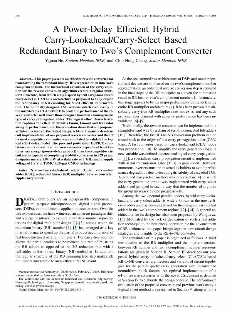
Fig. 2 illustrates the possible implementations of an 18-bitparallel-prefix carry computation with the uniform block factor(fixed radix) of 2 or 3, and nonuniform block factor (mixedradix) of 2 and 3. In this figure, the solid node represents theprefix operator, and the white hollow node o represents flow-through node or buffer. Fig. 2(a)–(c) depicts several carry gen-eration schemes for different block lengths of CSL, of 2,4, and 8 bits using a fixed block factor of . Similarly,Fig. 2(d) and 2(e) show two different schemes with and9 using a fixed block factor of 3. Various combinations ofand for mixed radix schemes are illustrated in Fig. 2(f)–(l).It is worth noting that, in the mixed radix schemes, the blockfactor is uniform within the same stage but nonuniform acrossstages. Completely mixed-radix carry generation trees are ana-lytically obscure to unification with the CSL sections for hybridCLA/CSL due to the immense number of complex formationsthat could be enumerated. The use of mixed radix cells withinthe same stage can easily annihilate the regularity and unneces-sarily complicate circuit and layout optimizations. Therefore, itwill only be considered on a sparse number of leave cells afterthe optimal regular mixed radix tree has been established andprovided its use will reduce the depth of the tree with minimalimpediment on layout regularity.
The speed of the hybrid CLA/CSL architecture is minimizedwhen the critical delay of the CLA network is commensuratewith that of the CSL sections. Therefore, for speed optimiza-tion, the block factor for the CLA complex gates at each stageof the hierarchy can be optimized to tailor to the optimal blocklength of CSL based on the implementations of the RCA andmultiplexer logics. The RB encoding has been beneficially ex-ploited in the RCA for the CSL circuit. Transistor-level cir-cuit design techniques have been applied to devise a new area-and power-efficient add-one circuit for the CSL adder. The de-tails of the novel CSL circuit for the hybrid CLA/CSL reverseconverter is best demonstrated with a 64-bit RB-to-NB con-verter to be presented in Section IV. The critical path for boththe CLA network and CSL sections are best evaluated with agood technology-independent model that account for loadingat transistor-level implementation to determine an optimizedmixed-radix CLA structure for various operand lengths. Thiswill be carried out in Section V.
Authorized licensed use limited to: Nanyang Technological University. Downloaded on February 25,2010 at 21:22:24 EST from IEEE Xplore. Restrictions apply.
340 IEEE TRANSACTIONS ON CIRCUITS AND SYSTEMS—I: REGULAR PAPERS, VOL. 55, NO. 1, FEBRUARY 2008
Fig. 2. 18-bit parallel-prefix carry generation with various block factors and block lengths of CSL. (a) b = 2 and m = 2. (b) b = 2 and m = 4. (c) b = 2 andm = 8. (d) b = 3 and m = 3. (e) b = 3 and m = 9. (f) b 2 f2; 3g and m = 2. (g) b 2 f2;3g and m = 3. (h) b 2 f2;3g and m = 4. (i) b 2 f2;3g andm = 6. (j) b 2 f2;3g and m = 6. (k) b 2 f2;3g and m = 8. (l) b 2 f2;3g and m = 9.
IV. IMPLEMENTATION OF A 64-b REVERSE CONVERTER
A. Architecture of 64-bit Reverse Converter
Here, a 64-bit RB-to-NB reverse converter is implementedwith our proposed CLA/CSL-based architecture. In principle,the block length of CSL can take any discrete value for any com-bination of the product of through at the transitive stage.In our implementation, we have limited the fan-in and fan-outof every circuit node to no more than 3 to avoid chaining morethan three p-channel/n-channel devices in series. Therefore, thelength of the CSL section will be a power of 2 or 3 or a multipleof 6 since the value of is confined to 2 or 3. We have selectedan optimal block length of CSL, , to match a mixed-radixcarry generation network from among the plausible topologiespresented in Section III based on an objective evaluation througha credible logical effort model. The model of evaluation and theresults will be discussed in detail in the next section.
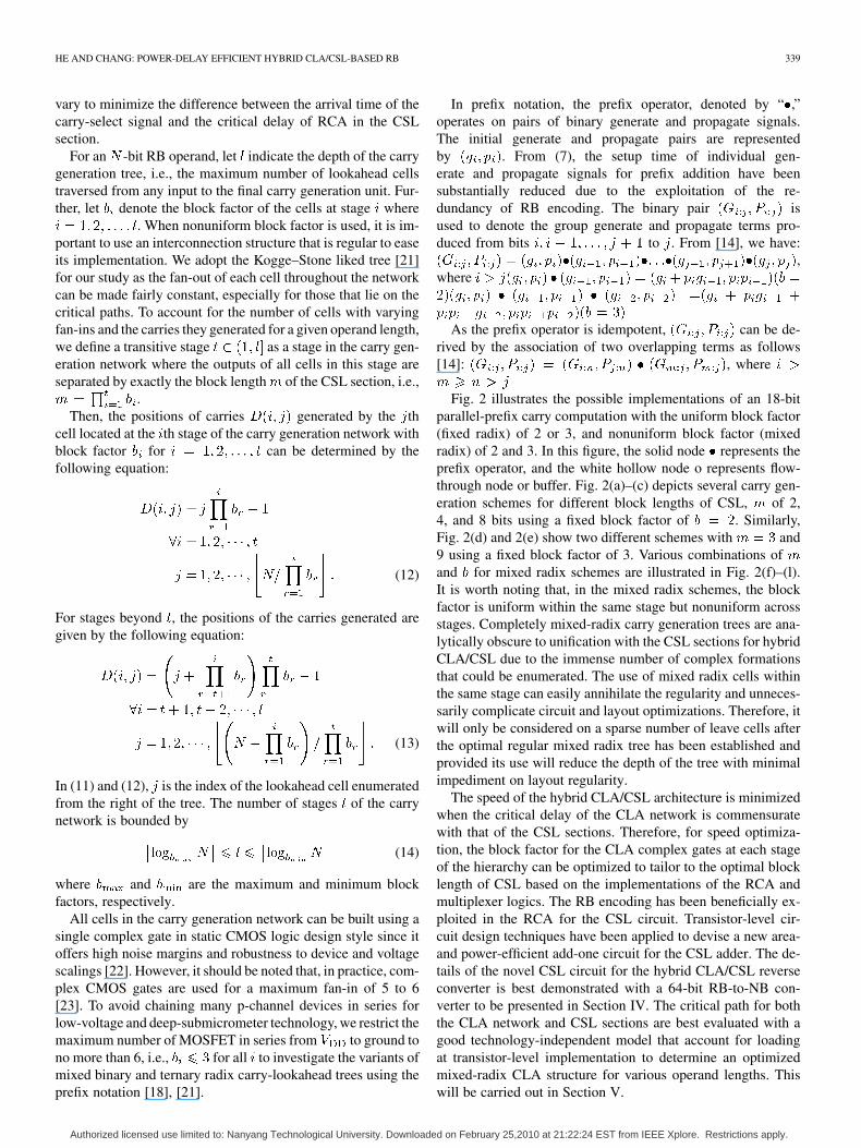
For CSL sections of constant block length , the im-plementation of a 64-bit reverse converter is not unique as thedepth of the carry generation tree can be either 5 or 6 according
to the block factors selected for each stage. An efficient imple-mentation of a 64-bit reverse converter architecture withis shown in Fig. 3. The numerical indices of and are used toidentify the stage numbers and the positions of the CLA cells ateach stage, respectively.
From Fig. 3, the regular carry generation network of the hy-brid CLA/CSL-based 64-bit reverse converter is optimized with
and . For , the tran-sitive stage occurs at stage 2 but instead of is selected to beof radix-3 to take advantage of the carry equation (10) with di-rect RB input in the first stage. From (12) and (13), the ten carryoutputs generated by the carry-lookahead network are , ,
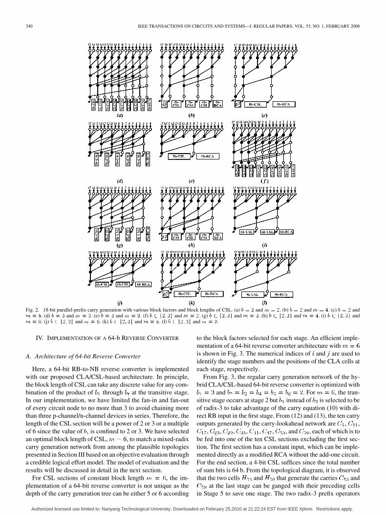
, , , , , , , and , each of which is tobe fed into one of the ten CSL sections excluding the first sec-tion. The first section has a constant input, which can be imple-mented directly as a modified RCA without the add-one circuit.For the end section, a 4-bit CSL suffices since the total numberof sum bits is 64 b. From the topological diagram, it is observedthat the two cells and that generate the carries and
at the last stage can be ganged with their preceding cellsin Stage 5 to save one stage. The two radix-3 prefix operators
Authorized licensed use limited to: Nanyang Technological University. Downloaded on February 25,2010 at 21:22:24 EST from IEEE Xplore. Restrictions apply.
HE AND CHANG: POWER-DELAY EFFICIENT HYBRID CLA/CSL-BASED RB 341
Fig. 3. Block diagram of the 64-bit reverse converter.
Fig. 4. Block diagram of the modified 64-bit reverse converter.
Fig. 5. Circuit implementation of G and P cells in the five-stage CLA network.
formed have the additional inputs stemmed from the first twobuffer nodes at Stage 4. Therefore, none of the operators has afan-out that exceeds three, and there is no change in the criticalpath except a slight perturbation to the wiring. Fig. 4 shows theblock diagram of the final five-stage reverse converter.
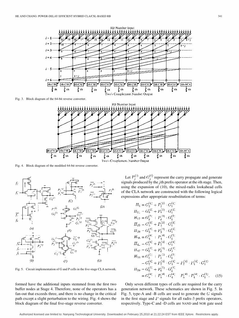
Let and represent the carry propagate and generatesignals produced by the th prefix operator at the th stage. Then,using the expansion of (10), the mixed-radix lookahead cellsof the CLA network are constructed with the following logicalexpressions after appropriate resubstitution of terms:
(15)
Only seven different types of cells are required for the carrygeneration network. These schematics are shown in Fig. 5. InFig. 5, type-A and -B cells are used to generate the signalsin the first stage and signals for all radix-3 prefix operators,respectively. Type-C and -D cells are NAND and NOR gate used
Authorized licensed use limited to: Nanyang Technological University. Downloaded on February 25,2010 at 21:22:24 EST from IEEE Xplore. Restrictions apply.
342 IEEE TRANSACTIONS ON CIRCUITS AND SYSTEMS—I: REGULAR PAPERS, VOL. 55, NO. 1, FEBRUARY 2008
to generate the signals for all radix-2 prefix operators. Type-Eand -F cells are complex gates used to generate the signals forall radix-2 prefix operators. A type-G cell is a complex gate usedmerely to generate and at Stage 5. It should be notedthat all of the and outputs alternate in polarities in the oddand even stages to unify the cells used. This unification not onlysimplifies and modularizes the circuit of the carry network butalso reduces its delay.
B. Design Considerations: Modified Add-One CSL Scheme
Among the arithmetic circuit design techniques, CSL hasemerged as an eminent approach to address the area–timetradeoff of CPA design. It exhibits the advantage of logarithmicgate depth as in any structure of the distant-carry adder family.When it is used together with CLA in the proposed RB-to-NBreverse converter, higher speed can be achieved at the expenseof increased hardware cost. Our approach to hybrid CLA/CSLdesign differs from others [13], [16], [20] in that we combine thelogic structure with a circuit technique to minimize the number oftransistors used in the CSL section without degrading its perfor-mance. Besides, we have fully tapped on the redundancy of RBencoding to halve the logics in the mandatory copy of the RCAof each CSL section, which further speeds up its sum and carrygeneration.
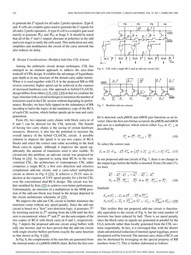
From (8), two separate carry chains with block carry-in of0 and 1 can be derived for the CSL network. The benefitof having two carry chains is the saving of certain hardwareresources. However, it also has the potential to increase theoverall latency of the hybrid CLA/CSL circuit. A possiblesolution to improve the speed is to use two copies of RCAblocks and select the correct sum value according to the finalblock carry-in signals. Although it improves the speed sig-nificantly, the amount of transistors used is also sizable. Tocircumvent this problem, an add-one circuit was proposed byChang in [24]. As opposed to using dual RCAs in the con-ventional CSL, the architecture of contemporary CSL addercomprises a single RCA, a first zero detection and selectivecomplement add-one circuit, and a carry-select multiplexercircuit as shown in Fig. 6 [24]. It achieves a 29.2% area re-duction at the expense of 5.9% speed penalty for a 64-bit CSLover the conventional dual-RCA design. The circuit was fur-ther modified by Kim [25] to achieve even better performance.Unfortunately, an omission of a multiplexer in the MSB posi-tion of the add-one block was found in the design depicted inthe circuit architecture schematic of [25].
We improve the add-one CSL circuit to further minimize thetransistor count without any speed penalty. Since the add-onecircuit is based on a “first” zero detection logic, it generatesby inverting each bit in starting from the LSB until the firstzero is encountered, where and are the sum outputs of thetwo copies of RCA with block carry-in 0 and 1, respectively.Fig. 7 depicts the proposed add-one circuit using buffers withonly one inverter, and we have proved that the add-one circuitwith single inverter buffers performs exactly the same functionas that shown in Fig. 6 [26].
In Fig. 6, the complements of the sum bits are generated fromthe internal nodes of a pMOS-nMOS chain. Before the first zero
Fig. 6. CSL with a single RCA and an add-one circuit [24].
Fig. 7. Modified add-one scheme.
bit is detected, each pMOS and nMOS pair functions as an in-verter. Once the first zero bit has occurred, the pMOS and nMOSpair acts as a multiplexer, which selects either or asdescribed by
(16)
To select the correct sum
(17)
In our proposed add-one circuit of Fig. 7, there is no change inthe output logic before the buffer is inserted. From (16) and (17),we have
(18)
Similarly
(19)
This verifies that our proposed add-one circuit is function-ally equivalent to the circuit of Fig. 6, but the total number ofinverters has been reduced by half. There is no speed penaltysince the block carry-in signals are generated in parallel by theCLA network rather than locally generated from the CSL sec-tions sequentially. In fact, it is envisaged that, with the shorterchain and potential reduction of internal signal togglings, powerdissipation will be lowered. The internal carry chain of RCA canalso be shortened by leveraging on the special property of RBnumbers from (7). This is further elaborated as follows.
Authorized licensed use limited to: Nanyang Technological University. Downloaded on February 25,2010 at 21:22:24 EST from IEEE Xplore. Restrictions apply.

HE AND CHANG: POWER-DELAY EFFICIENT HYBRID CLA/CSL-BASED RB 343
From the original input and of the RB number to beconverted, the internal carry signal of a RCA can be simplifiedas follows:
... (20)
Therefore, the carry generation chain in the proposed RCAcan be readily implemented in branch-based logic style to min-imize the number of internal connections [20]. Branch-basedcircuits possess high noise margins and robustness to voltageand device scaling reminiscent of classical static CMOS designstyle. From (7), by exploiting the RB encoding, both the sum bitsand its complement can be generated simultaneously using thenew XOR/XNOR circuit [27] to enhance their driving capability.Comparing with the full adder of Fig. 6, which requires two XOR
gates for the sum generation, the propagation delay has been re-duced. With the cogeneration of complementary sum bits, thethreshold voltage drop problem of pass transistors [28] inthe add-one circuit of Fig. 6 can also be overcome by replacingthem with transmission gates.
The modified 6-bit ripple-carry chain and the new add-onecircuit are integrated into a 6-bit CSL as shown in Fig. 8. Iden-tical circuit topology for the odd and even carry-generation cellsare used to implement the carry signals with alternating polar-ities of inputs and outputs in the modified ripple-carry chain.At the bottom, the final sum of CSL can be generated fromthe add-one circuit by using only a group of NAND gates andmultiplexers. It realizes the following logic equation derivedfrom (17):
(21)
The output is selected from the two data input signals andits complement. The select signal is generated by aNAND gate from the carry-in and the complement of .Thus, we can eliminate one inverter in each buffer from the cor-responding block of Fig. 6 without violating its functionality.The NAND gates also function as buffers to improve the drivingcapability.
V. PERFORMANCE EVALUATION
This section evaluates the performance of our newly pro-posed converter architecture and compares it with three com-petitive converters [4], [10], [11]. According to Section III-B,a fixed-size operand can have several ramifications of architec-ture depending on the block factors and block lengths of theCSL sections chosen for the implementation. Therefore, we areinterested to find an optimum realization for a given operandsize from among the feasible solutions of our base converterarchitecture.
Fig. 8. 6-bit carry-select block with modified add-one scheme.
A critical path is the worst-case delay from any input transi-tion to the latest output transition over all possible input patterns.As pointed out in [12], comparison of complex gates based ona unit gate delay model in CMOS digital circuits can be mis-leading because the delays are largely influenced by their cir-cuit topology (fan-in) and loading (fan-out). Recently, a popularmethod called logical effort (LE) based on the RC delay modelprovides a convenient shorthand for more realistic speed estima-tion of CMOS digital circuits [29], [30]. It captures reasonablywell the effect of transistor sizing for different transistor-levelimplementations according to the critical paths of the corre-sponding circuit architectures and their loading. The accuracyof LE estimation has been attested by reliable circuit simula-tion tool HSPICE by several researchers [30]–[32]. It thereforeprovides a fast and consistent means to evaluate the potentialperformance of a new reverse converter architecture as well asthe relative performances among different converters.
Using the logic effort model, we perform the complexityanalysis of our proposed reverse converter for operand lengthsof 8, 16, 32, 64, and 128 with various block factors of CLA andblock lengths of CSL. The results are shown in Table I. Notethat the delay time is normalized to that of a fanout-of-4 (FO4)inverter delay [29]. Although for certain operand lengths thereexist more than one implementations correspond to certainblock factor and block length of CSL, only the fastest solutionis presented in Table I. Since the transistor count of a circuithas an indirect correlation to the VLSI area, the number oftransistors in each circuit is accounted for and summarizedin Table II. The area-delay products (ATs) are also providedin Table III, where the area is measured in terms of transistorcount, the AT values are normalized by the AT value of the caseof and , and the obtained ratios are expressed
Authorized licensed use limited to: Nanyang Technological University. Downloaded on February 25,2010 at 21:22:24 EST from IEEE Xplore. Restrictions apply.
344 IEEE TRANSACTIONS ON CIRCUITS AND SYSTEMS—I: REGULAR PAPERS, VOL. 55, NO. 1, FEBRUARY 2008
TABLE ICOMPARISON OF DELAY FOR DIFFERENT COMBINATIONS OF BLOCK FACTORS
OF CLA AND BLOCK LENGTHS OF CSL
TABLE IICOMPARISON OF TRANSISTOR COUNT FOR DIFFERENT COMBINATIONS OF
BLOCK FACTORS OF CLA AND BLOCK LENGTHS OF CSL
TABLE IIICOMPARISON OF AREA–DELAY PRODUCT FOR DIFFERENT COMBINATIONS OF
BLOCK FACTORS OF CLA AND BLOCK LENGTHS OF CSL
in percentage. From these results, the most optimum reverseconverter with the minimum AT for each operand length isselected to compare against other fast reverse converters.
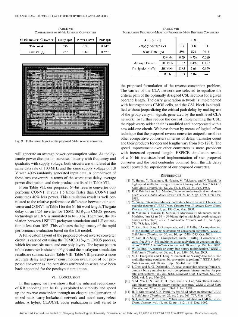
For a fair comparison, the contender circuits CONV1 [4],CONV2 [10], and CONV3 [11] were replicated as reported inthe literature. For high-speed operation, CONV1 is optimizedusing CSL with minimized critical path. CONV2 is a simplifiedCSL, which uses inverters instead of complex CMOS circuits toproduce the “generate signal ” and the “propagate signal ”according to the consideration presented in [10]. CONV3 usespass transistor logic. Hence, buffers are inserted in every twotransmission gates to prevent the signal from decaying.
The delays of different reverse converters based on the LEmodel for various operand lengths are tabulated in Table IV.The number of transistors required by each converter is shownin Table V. The ATs are also provided in Table VI to comparethe combined criterion of cost and performance of different re-verse converters. In Table VI, the AT cost of CONV3 is used
TABLE IVCOMPARISON OF DELAY OF DIFFERENT CONVERTERS
TABLE VCOMPARISON OF TRANSISTOR COUNT OF DIFFERENT CONVERTERS
TABLE VICOMPARISON OF AREA–DELAY PRODUCT OF DIFFERENT CONVERTERS
as a reference to normalize the AT cost of all other converters.From the above tables, it is evident that our newly proposed re-verse converter has the minimum AT for any operand length incomparison with other converters. More importantly, the delayof our proposed converter does not escalate with the increaseof operand length as badly as other converters do. As the wordlength increases, the improvement in the combined area–timeperformance becomes more prominent.
To validate and reinforce the results estimated by the LEmodel, we implement two 64-bit reverse converters. One is ourproposed converter and the other is CONV1 since it is the mostcompetitive one according to its performance evaluated earlierin Tables IV–VI. As power consumption has become an increas-ingly important performance criterion, “using a design that isfast enough and consumes the least power” might be a better ruleof thumb than “using the fastest design” [16]. Therefore, besidesthe worst case delay, the converters are also simulated for theiraverage power consumptions. For a fair comparison, both cir-cuits are optimized in speed according to the critical paths esti-mated from the architectures. The optimization process was car-ried out recursively until all transistor sizes converged [28]. Allof the circuits are simulated using HSPICE based on the TSMC0.18- m CMOS process model. For each simulation, HSPICE
Authorized licensed use limited to: Nanyang Technological University. Downloaded on February 25,2010 at 21:22:24 EST from IEEE Xplore. Restrictions apply.
HE AND CHANG: POWER-DELAY EFFICIENT HYBRID CLA/CSL-BASED RB 345
TABLE VIICOMPARISONS OF 64-bit REVERSE CONVERTERS
Fig. 9. Full-custom layout of the proposed 64-bit reverse converter.
will generate an average power consumption value. As the dy-namic power dissipation increases linearly with frequency andquadratic with supply voltage, both circuits are simulated at thesame data rate of 100 MHz and the same supply voltage of 1.8V with 4096 randomly generated input data. A comparison ofthese two converters in terms of the worst case delay, averagepower dissipation, and their product are listed in Table VII.
From Table VII, our proposed 64-bit reverse converter out-performs CONV1. It runs 1.5 times faster than CONV1 andconsumes 40% less power. This simulation result is well cor-related to the relative performance difference between our con-verter and CONV1 in Table I for the 64-bit word length. The gatedelay of an FO4 inverter for TSMC 0.18- m CMOS processtechnology at 1.8 V is simulated to be 70 ps. Therefore, the de-viation between HSPICE prelayout simulation and LE estima-tion is less than 10%. This validates the legitimacy of the rapidperformance evaluation based on the LE model.
A full-custom layout of the proposed 64-bit reverse convertercircuit is carried out using the TSMC 0.18- m CMOS process,which features six metal and one poly layers. The layout patternof the converter is shown in Fig. 9 and the postlayout simulationresults are summarized in Table VIII. Table VIII presents a moreaccurate delay and power consumption evaluation of our pro-posed converter as the parasitics attributed to wires have beenback annotated for the postlayout simulation.
VI. CONCLUSION
In this paper, we have shown that the inherent redundancyof RB encoding can be fully exploited to simplify and speedup the reverse conversion through an elegant amalgamation ofmixed-radix carry-lookahead network and novel carry-selectadder. A hybrid CLA/CSL adder realization is well suited to
TABLE VIIIPOSTLAYOUT FIGURE-OF-MERIT OF PROPOSED 64-bit REVERSE CONVERTER
the proposed formulation of the reverse conversion problem.The carries of the CLA network are selected to equalize thecritical path of the optimally designed CSL sections for a givenoperand length. The carry generation network is implementedwith heterogeneous CMOS cells, and the CSL block is simpli-fied without jeopardizing the critical path delay by making useof the group carry-in signals generated by the multilevel CLAnetwork. To further reduce the cost of implementing the CSL,the ripple-carry adder chain is modified and incorporated with anew add-one circuit. We have shown by means of logical efforttechnique that the proposed reverse converter outperforms threeother competitive converters in terms of delay, transistor countand their products for operand lengths vary from 8 to 128 b. Thespeed improvement over other converters is more providentwith increased operand length. HSPICE simulation resultsof a 64-bit transistor-level implementation of our proposedconverter and the best contender obtained from the LE delaymodel proved the superiority of our proposed converter.
REFERENCES
[1] Y. Harata, Y. Nakamura, H. Nagase, M. Takigawa, and N. Takagi, “Ahigh-speed multiplier using a redundant binary adder tree,” IEEE J.Solid-State Circuits, vol. SC-22, no. 1, pp. 28–34, Feb. 1987.
[2] K. K. Primlani and J. L. Meador, “A nonredundant-radix-4 serial multi-plier,” IEEE J. Solid-State Circuits, vol. 24, no. 6, pp. 1729–1736, Dec.1989.
[3] Y. Wang, “Residue-to-binary converters based on new Chinese re-mainder theorems,” IEEE Trans. Circuits Syst. II, Analog Digit. SignalProcess., vol. 47, no. 3, pp. 192–206, Mar. 2000.
[4] H. Makino, Y. Nakase, H. Suzuki, H. Morinaka, H. Shinohara, and K.Mashiko, “An 8.8 ns 54� 54-bit multiplier with high speed redundantbinary architecture,” IEEE J. Solid-State Circuits, vol. 31, no. 6, pp.773–783, Jun. 1996.
[5] Y. Kim, B.-S. Song, J. Grosspietsch, and S. F. Gillig, “A carry-free 54b� 54b multiplier using equivalent bit conversion algorithm,” IEEE J.Solid-State Circuits, vol. 36, no. 10, pp. 1538–1545, Oct. 2001.
[6] Y. Kim, B.-S. Song, J. Grosspietsch, and S. F. Gillig, “Correction to ‘acarry-free 54b � 54b multiplier using equivalent bit conversion algo-rithm’,” IEEE J. Solid-State Circuits, vol. 38, no. 1, p. 159, Jan. 2003.
[7] W. Rulling, “A remark on carry-free binary multiplication,” IEEE J.Solid-State Circuits, vol. 38, no. 1, pp. 159–160, Jan. 2003.
[8] M. D. Ercegovac and T. Lang, “Comments on ‘a carry-free 54b� 54bmultiplier using equivalent bit conversion algorithm’,” IEEE J. Solid-State Circuits, vol. 38, no. 1, pp. 160–161, Jan. 2003.
[9] I. Choo and R. G. Deshmukh, “A novel conversion scheme from a re-dundant binary number to two’s complement binary number for par-allel architectures,” in Proc. IEEE Southeast Conf., Clemson, SC, Apr.2001, vol. 2, pp. 196–201.
[10] S. M. Yen, C. S. Laih, C. H. Chen, and J. Y. Lee, “An efficient redun-dant-binary number to binary number converter,” IEEE J. Solid-StateCircuits, vol. 27, no. 1, pp. 109–112, Jan. 1992.
[11] H. R. Srinivas and K. K. Parhi, “A fast VLSI adder architecture,” IEEEJ. Solid-State Circuits, vol. 27, no. 5, pp. 761–767, May 1992.
[12] N. Quach and M. J. Flynn, “High speed addition in CMOS,” IEEETrans. Comput., vol. 41, no. 12, pp. 1612–1615, Dec. 1992.
Authorized licensed use limited to: Nanyang Technological University. Downloaded on February 25,2010 at 21:22:24 EST from IEEE Xplore. Restrictions apply.

346 IEEE TRANSACTIONS ON CIRCUITS AND SYSTEMS—I: REGULAR PAPERS, VOL. 55, NO. 1, FEBRUARY 2008
[13] T. Lynch and E. E. Swartzlander, Jr., “A spanning tree carry lookaheadadder,” IEEE Trans. Comput., vol. 41, no. 8, pp. 931–939, Aug. 1992.
[14] V. Kantabutra, “A recursive carry-lookahead/carry-select hybridadder,” IEEE Trans. Comput., vol. 42, no. 12, pp. 1495–1499, Dec.1993.
[15] Y. Wang, C. Pai, and X. Song, “The design of hybrid carry-lookahead/carry-select adders,” IEEE Trans. Circuits Syst. II, Analog Digit. SignalProcess., vol. 49, no. 1, pp. 16–24, Jan. 2002.
[16] C. Nagendra, M. J. Irwin, and R. M. Owens, “Area-time-power trade-offs in parallel adders,” IEEE Trans. Circuits Syst. II, Analog Digit.Signal Process., vol. 43, no. 10, pp. 689–702, Oct. 1996.
[17] T. P. Kelliher, R. M. Owens, M. J. Irwin, and T.-T. Hwang, “ELM—Afast addition algorithm discovered by a program,” IBM J. Res. Dev.,vol. 41, no. 9, pp. 1181–1184, Sep. 1992.
[18] R. P. Brent and H. T. Kung, “A regular layout for parallel adders,” IEEETrans. Comput., vol. C-31, no. 3, pp. 260–264, Mar. 1982.
[19] H. Ling, “High speed binary adder,” IBM J. Res. Dev., pp. 156–166,May 1981.
[20] A. Neve, H. Schettler, T. Ludwig, and D. Flandre, “Power-delayproduct minimization in high-performance 64-bit carry-select adders,”IEEE Trans. VLSI Syst., vol. 12, no. 3, pp. 235–244, Mar. 2004.
[21] P. M. Kogge and H. S. Stone, “A parallel algorithm for the efficientsolution of a general class of recurrence equations,” IEEE Trans.Comput., vol. 22, no. 8, pp. 786–793, Aug. 1973.
[22] M. Alioto and G. Palumbo, “Analysis and comparison on full adderblock in submicron technology,” IEEE Trans. VLSI Syst., vol. 10, no.6, pp. 806–823, Dec. 2002.
[23] A. Bellaouar and M. I. Elmasry, Low-Power Digital VLSI Design: Cir-cuits and Systems. Dordrectht, The Netherlands: Kluwer, 1995.
[24] T. Y. Chang and M. J. Hsiao, “Carry-select adder using single ripple-carry adder,” Electron. Lett., vol. 34, no. 22, pp. 2101–2103, Oct. 1998.
[25] Y. Kim and L. S. Kim, “64-bit carry-select adder with reduced area,”Electron. Lett., vol. 37, no. 10, pp. 614–615, May 2001.
[26] Y. He, C. H. Chang, and J. Gu, “An area efficient 64-bit square rootcarry-select adder for low power applications,” in Proc. IEEE Int.Symp. Circuits Syst. (ISCAS’2005), Kobe, Japan, May 2005, vol. 4,pp. 4082–4085.
[27] C. H. Chang, J. Gu, and M. Zhang, “Ultra low voltage, low powerCMOS 4-2 and 5-2 compressors for fast arithmetic circuits,” IEEETrans. Circuits Syst. I, Reg. Papers, vol. 51, no. 10, pp. 1985–1997,Oct. 2004.
[28] C. H. Chang, J. Gu, and M. Zhang, “A review of 0.18- �m full adderperformances for tree structured arithmetic circuits,” IEEE Trans. VLSISyst., vol. 13, no. 6, pp. 686–695, Jun. 2005.
[29] I. Sutherland, R. Sproull, and D. Harris, Logical Effort: Designing FastCMOS Circuits. San Mateo, CA: Morgan Kaufmann, 1999.
[30] D. Harris and I. Sutherland, “Logical effort of carry propagate adders,”in Proc. 37th IEEE Asilomar Conf. Signals, Syst., Comput. (ACSSC),Pacific Grove, CA, Nov. 2003, vol. 1, pp. 873–878.
[31] H. Q. Dao and V. Oklobdzija, “Application of logical effort on delayanalysis of 64-bit static carry-lookahead adder,” in Proc. 35th IEEEAsilomar Conf. Signals, Syst., Comput. (ACSSC), Pacific Grove, CA,Nov. 2001, vol. 2, pp. 1322–1324.
[32] V. G. Oklobdzija, B. R. Zeydel, H. Dao, S. Mathew, and R. Krish-namurthy, “Energy-delay estimation technique for high-performancemicroprocessor VLSI adders,” in Proc. 16th IEEE Symp. Comput.Arithmetic (ARITH), Santiago de Compostela, Spain, Jun. 2003, pp.272–279.
Yajuan He (S’05) received the B.S. degree inelectronic science and technology from the EastChina Normal University (ECNU), Shanghai, China,in 2001. She is currently working toward the Ph.D.degree at the Nanyang Technological University(NTU), Singapore.
From 2001 to 2002, she was an RTP DigitalIC Designer with the Institute of Microelectronics(IME), Singapore. In 2007, she joined STMicroelec-tronics, Singapore, as a Digital IC Design Engineerin the Smartcards Division, Asia-Pacific Design
Center (APDC). Her research interests include computer arithmetic circuitsand low-power IC design.
Chip-Hong Chang (S’92–M’98–SM’03) receivedthe B.Eng. (Hons) degree from National Universityof Singapore, Singapore, in 1989, and the M.Eng.and Ph.D. degrees from Nanyang TechnologicalUniversity (NTU), Singapore, in 1993 and 1998,respectively.
He served as a Technical Consultant in industryprior to joining the School of Electrical and Elec-tronic Engineering, NTU, in 1999, where he is nowan Associate Professor. He holds joint appointmentsat the university as Deputy Director of the Centre for
High Performance Embedded Systems (CHiPES) since 2000 and Program Di-rector of the Centre for Integrated Circuits and Systems (CICS) since 2003.His current research interests include low-power arithmetic circuits, constraineddriven architectures for digital signal processing, and digital watermarking forIP protection. He has published three book chapters and more than 120 researchpapers in international refereed journals and conferences.
Dr. Chang is a Fellow of IET.
Authorized licensed use limited to: Nanyang Technological University. Downloaded on February 25,2010 at 21:22:24 EST from IEEE Xplore. Restrictions apply.
Related Documents