This is a repository copy of A method for the measurement of shielding effectiveness of planar samples requiring no sample edge preparation or contact . White Rose Research Online URL for this paper: https://eprints.whiterose.ac.uk/80621/ Version: Accepted Version Article: Marvin, Andrew C. orcid.org/0000-0003-2590-5335, Dawson, Linda, Flintoft, Ian David orcid.org/0000-0003-3153-8447 et al. (1 more author) (2009) A method for the measurement of shielding effectiveness of planar samples requiring no sample edge preparation or contact. IEEE Transactions on Electromagnetic Compatibility. pp. 255-262. ISSN 0018-9375 https://doi.org/10.1109/TEMC.2009.2015147 [email protected] https://eprints.whiterose.ac.uk/ Reuse Items deposited in White Rose Research Online are protected by copyright, with all rights reserved unless indicated otherwise. They may be downloaded and/or printed for private study, or other acts as permitted by national copyright laws. The publisher or other rights holders may allow further reproduction and re-use of the full text version. This is indicated by the licence information on the White Rose Research Online record for the item. Takedown If you consider content in White Rose Research Online to be in breach of UK law, please notify us by emailing [email protected] including the URL of the record and the reason for the withdrawal request.

Welcome message from author
This document is posted to help you gain knowledge. Please leave a comment to let me know what you think about it! Share it to your friends and learn new things together.
Transcript
This is a repository copy of A method for the measurement of shielding effectiveness of planar samples requiring no sample edge preparation or contact.
White Rose Research Online URL for this paper:https://eprints.whiterose.ac.uk/80621/
Version: Accepted Version
Article:
Marvin, Andrew C. orcid.org/0000-0003-2590-5335, Dawson, Linda, Flintoft, Ian David orcid.org/0000-0003-3153-8447 et al. (1 more author) (2009) A method for the measurement of shielding effectiveness of planar samples requiring no sample edge preparation or contact. IEEE Transactions on Electromagnetic Compatibility. pp. 255-262. ISSN 0018-9375
https://doi.org/10.1109/TEMC.2009.2015147
[email protected]://eprints.whiterose.ac.uk/
Reuse
Items deposited in White Rose Research Online are protected by copyright, with all rights reserved unless indicated otherwise. They may be downloaded and/or printed for private study, or other acts as permitted by national copyright laws. The publisher or other rights holders may allow further reproduction and re-use of the full text version. This is indicated by the licence information on the White Rose Research Online record for the item.
Takedown
If you consider content in White Rose Research Online to be in breach of UK law, please notify us by emailing [email protected] including the URL of the record and the reason for the withdrawal request.
© 2009 IEEE. Personal use of this material is permitted. Permission from IEEE must be obtained for all other uses, in any
current or future media, including reprinting/republishing this material for advertising or promotional purposes, creating new
collective works, for resale or redistribution to servers or lists, or reuse of any copyrighted component of this work in other
works.
Andrew C Marvin, Linda Dawson, Ian Flintoft and John Dawson, “A Method for the Measurement of Shielding Effectiveness of
Planar Samples Requiring no Sample Edge Preparation or Contact”, IEEE Transactions on Electromagnetic Compatibility,
Vol. 51, No. 2, May 2009, pp. 255-262.
DOI: http://dx.doi.org/10.1109/TEMC.2009.2015147
keywords: Shielding Effectiveness, Shielding Measurements
URL: http://ieeexplore.ieee.org/xpl/articleDetails.jsp?arnumber=4812060
Abstract—A method is presented for the measurement of shielding effectiveness of planar materials with non-conducting surfaces
such as carbon fibre composites. The method overcomes edge termination problems with such materials by absorbing edge-diffracted
energy. A dynamic range of up to 100 dB has been demonstrated over a frequency range of 1 to 8.5 GHz depending on the size of the
sample under test. Comparison with ASTM D4935 and nested reverberation measurements of shielding effectiveness shows good
agreement.
Index Terms—Shielding Effectiveness, Shielding Measurements
I. INTRODUCTION
he measurement of the shielding effectiveness (SE) of a planar material sample is required in order to predict the suitability
of the material to form an enclosed electromagnetic shield. A typical shielded enclosure has an ultimate shielding
performance that is limited by the shielding performance of its structural features such as apertures penetrations and joints. For a
high quality shielded enclosure the SE expressed logarithmically may exceed 100 dB when the enclosure is first commissioned.
Typical equipment enclosures, or enclosures that have a secondary shielding requirement, such a vehicle bodies, may have SE
values in the range 10 dB to 80 dB. This lower performance is a consequence of the structural features and the consequent
requirement for the shielding performance of the structural material is lower, typically no more than 90 dB. Any sheet metal used
as a structural material will have a SE considerably in excess of 90 dB. Structural materials formed from metallised plastic or
other non-conducting substrates with an internal conducting component, such as carbon fibre re-enforced composite (CFC), may
have SE values in the range below 90 dB and thus require measurement.
Such materials are conventionally measured in test systems that require a planar sample of the material to be placed across an
aperture or within the cross-section of a transmission line. Examples are the use of nested reverberation chambers (NRC) [1,2],
nested anechoic chambers and coaxial TEM waveguides, typically the standard ASTM cell [3]. In each of these systems the
measured reduction of transmitted electromagnetic energy (insertion loss) through the aperture or cell with the sample present is
compared to that without the sample present and the data is processed to estimate the SE of the sample material. With the sample
present the energy flow is through the sample and possibly around the edge of the sample if a good conducting contact between
the outer edge of the sample and the inner edge of the aperture/cell is not maintained along the entire sample perimeter. The edge
contact requirement has been overcome in some coaxial systems [4,5] but can be a major source of measurement error in other
systems that require contact with a buried conducting material or samples with conductor on one side only. These problems are
particularly acute as the frequency of the measurement increases and especially in the microwave frequency range where the
structural dimensions of the sample material features, for example the weave in the fabric of a composite material, become
comparable to the wavelength.
II. PROPOSED SYSTEM
In this paper we describe a measurement system that overcomes the edge contact problems by eliminating its requirement.
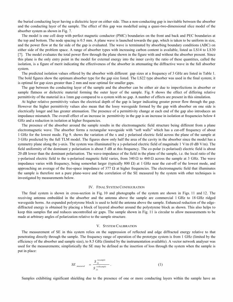
Such a technique has been proposed before, where the planar sample is illuminated from one side and the transmitted energy is
received on the other side along with edge diffracted energy and energy reflected from surrounding objects [6]. These latter
unwanted artefacts, which follow a longer propagation path, are time gated out to leave the energy transmitted through the
sample. The measurement dynamic range of this technique is limited to around 50 dB to 60 dB by the imperfections in the time
gating process that results in some residual unwanted energy. The system is shown in outline diagrammatic form in Fig. 1.
A Method for the Measurement of Shielding
Effectiveness of Planar Samples Requiring no
Sample Edge Preparation or Contact
Andrew C Marvin, Senior Member IEEE, Linda Dawson, Ian Flintoft, Member IEEE
and John Dawson, Member IEEE
T
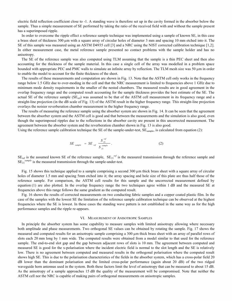
The approach taken here is to accept the edge diffracted energy but to absorb it after diffraction in an absorber assembly
fabricated from proprietary carbon loaded polyurethane foam [7]. Fig. 2 shows the principle of the new system where the
absorber reduces the effect of the diffracted and reflected energy. Absorber has previously been used to attenuate diffracted
energy in specialized gasket shielding measurement systems [8], however the effectiveness and optimization of the absorber has
not being addressed. In the work reported here the absorber is explicitly used for the termination of planar samples and the
measurements system is optimized for composite materials.
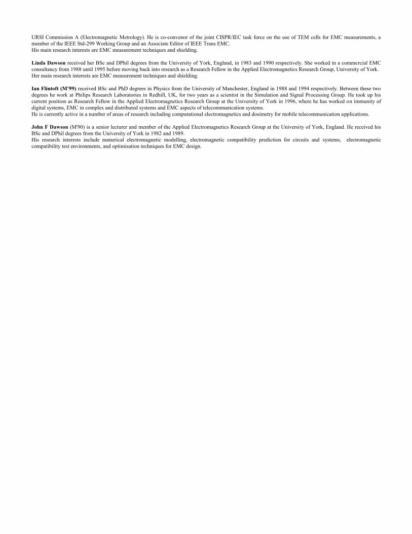
The prototype system is shown in Fig. 3. The dimensions of the prototype system are 600 mm by 600 mm by 330 mm with the
aperture in the absorber being 140 mm by 150 mm, chosen to fit the dimensions of the ridged waveguide horn used as the
receiving antenna (embedded in the bottom of the cavity). In practice larger apertures could be used. The absorber is enclosed in
a metal box and the receive antenna signal is fed to a port on one side of the box using semi-rigid cable embedded in the
absorber.
III. PREDICTED PERFORMANCE OF THE SYSTEM
The absorber structure was modelled in order to predict and optimise its performance. The dynamic range of the system
depends on the attenuation of the incident energy through the absorber underneath the sample and is therefore determined by the
sample size and the attenuation constant of the absorber. Absorbers are commercially available with a variety of different
attenuation levels and the question of which type provides the optimal performance arises when practical limitations of the
absorber system are taken into account. The model was also used to evaluate the minimum size of sample required for a given
dynamic range and to verify that the system was actually measuring the SE of the samples.
The Transmission Line Matrix (TLM) algorithm with a node spacing of 5 mm was used to construct a three-dimensional model
of the absorber system depicted in Fig. 2 [9]. The model, shown in Fig. 4, included the metal outer box, the absorber, the cavity
and the sample. A symmetry plane through the centre of the system was utilised to improve the computational efficiency. The
model did not include representations of the horn antennas; instead a plane wave was used for the excitation and the field at the
centre of the cavity was observed to estimate the transmission through the sample. The frequency dependent conductivity and
permittivity of the absorber were taken from the manufacturers data sheets [7]. The node spacing of 5 mm is adequate to give a
resolution of one-tenth of a wavelength up to 6 GHz; note that the relative permittivity of the absorber, which is typically around
10 at 1 GHz, falls rapidly with frequency. The sample was modelled using TLM thin boundaries, described in more detail below.
Fig. 5 shows the results of the model’s estimate of the dynamic range of the system obtained by comparing the electric field
computed in the antenna cavity with no sample present to the electric field at the sample location with a 300 mm square perfect
electric conductor (PEC) sheet used in place of the material sample. The PEC sheet has effectively infinite shielding effectiveness
in the model so the predicted SE in Fig. 5 indicates the energy diffracted around the sample that is not blocked by the absorber.
The points are the computed result and the line is the measured result. The noise on the measured result above 4 GHz is the
equipment noise floor. The dynamic range of the system is greater for larger samples at lower frequencies due to the increasing
attenuation of energy coupled around the edge of the sample.
Verification that the system was indeed measuring SE was obtained by modelling samples with different characteristics using a
sub-scale partially reflecting/transmitting TLM boundary with defined transmission coefficients [10]. This is the TLM equivalent
of impedance boundary models in FDTD, which are often used to simulate composite materials [11]. The TLM boundary model
is parameterised by the scattering matrix of the transverse field components at the boundary. To show more explicitly the effect
of the sample size and absorber characteristics on the dynamic range of the system a range of “fictitious” samples with frequency
independent transmission coefficients ranging from 20 dB to 80 dB were modelled (the reflection coefficient is chosen to ensure
energy conservation and provide a little absorption in the boundary). The transmission coefficient defined for the boundary is
implicitly the plane-wave infinite planar SE of the “fictitious” sample.
Fig. 6 shows the results of this simulation for samples with SE values in the range 20 dB to 80 dB. In these simulations a
frequency independent model of the absorber was used for computational efficiency, taking the manufacturers material
parameters at 3 GHz. The ratio of the predicted field value in the cavity below the sample to the predicted value in the cavity with
the sample removed was evaluated.
It can be seen that the predicted SE values are very close to the infinite plane-wave SE values of the computational samples.
The low frequency fall-off of the predicted SE value is due to energy leakage around the edge of the sample. The ultimate
predicted dynamic range for a sample of this size is that obtained for the PEC sheet.
The energy leakage around the sample edge is reduced by the presence of the absorber, however the SE obtained in the
prototype system was lower than predicted. This was found to be a function of the flatness of the sample and the absorber. Any
air gap between the sample and absorber allowed energy to be guided between them. In the simulations described above the
interface between the sample and the absorber was idealised, with the absorber in direct contact with the sample over the entire
area of overlap between the sample and absorber. In the practical system direct contact cannot be achieved over the whole
overlap region so the dynamic range is further limited. Also, many composite samples are likely to be layered in structure with
the buried conducting layer having a dielectric layer on either side. Thus a non-conducting gap is inevitable between the absorber
and the conducting layer of the sample. The effect of this gap was modelled using a quasi-two-dimensional slice model of the
absorber system as shown in Fig. 7.
The model is one cell deep with perfect magnetic conductor (PMC) boundaries on the front and back and PEC boundaries at
the top and bottom. The node spacing is 0.5 mm. A plane wave is launched towards the gap, which is taken to be uniform in size,
and the power flow at the far side of the gap is evaluated. The wave is terminated by absorbing boundary conditions (ABC) on
either side of the problem space. A range of absorber types with increasing carbon content is available, listed as LS14 to LS30
[7]. The model evaluates the total power flow through the plane shown in the figure with and without the absorber present. Since
this plane is the only entry point in the model for external energy into the inner cavity the ratio of these quantities, called the
isolation, is a figure of merit indicating the effectiveness of the absorber in attenuating the diffractive wave in the full absorber
system.
The predicted isolation values offered by the absorber with different gap sizes at a frequency of 3 GHz are listed in Table 1.
The bold figures show the optimum absorber type for the gap size listed. The LS22 type absorber was used in the final system; it
is optimal for gap sizes greater than 2 mm and near optimal for smaller gaps.
The gap between the conducting layer of the sample and the absorber can be either air due to imperfections in absorber or
sample flatness or dielectric material forming the outer layer of the sample. Fig. 8 shows the effect of differing relative
permittivity of the material in a 1mm gap compared to a system with no gap. A number of effects are present in this simulation.
At higher relative permittivity values the electrical depth of the gap is larger indicating greater power flow through the gap.
However the higher permittivity values also mean that the lossy waveguide formed by the gap with absorber on one side is
electrically longer and has greater attenuation. The presence of a permittivity change at each end of the gap also introduces an
impedance mismatch. The overall effect of an increase in permittivity in the gap is an increase in isolation at frequencies below 4
GHz and a reduction in isolation at higher frequencies.
The presence of the absorber around the sample results in the electromagnetic field structure being different from a plane
electromagnetic wave. The absorber forms a rectangular waveguide with “soft walls” which has a cut-off frequency of about
1 GHz for the lowest mode. Fig 9. shows the variation of the x and y polarised electric field across the plane of the sample at
3 GHz predicted by the full TLM model. The figures show only half the area of the cavity in the absorber since the model has a
symmetry plane along the y-axis. The system was illuminated by a y-polarised electric field of magnitude 1 V/m (0 dB V/m). The
field uniformity of the dominant y polarisation is about 5 dB at this frequency. The co-polar (x-polarised) electric field is about
20 dB lower than the dominant polarisation. The wave-impedance of the field in the plane of the sample, i.e. the local ratio of the
y-polarised electric field to the x-polarised magnetic field varies, from 340 to 460 across the sample at 3 GHz. The wave
impedance varies with frequency, being somewhat larger (typically 800 ) at 1 GHz near the cut-off of the lowest mode, and
approaching an average of the free-space impedance of 377 at higher frequencies. The electromagnetic field that illuminates
the sample is therefore not a pure plane-wave and the correlation of the SE measured by the system with other techniques is
investigated by measurements below.
IV. FINAL SYSTEM CONFIGURATION
The final system is shown in cross-section in Fig. 10 and photographs of the system are shown in Figs. 11 and 12. The
receiving antenna embedded in the absorber and the antenna above the sample are commercial 1 GHz to 18 GHz ridged
waveguide horns. An expanded polystyrene block is used to hold the antenna above the sample. Enhanced reduction of the edge-
diffracted energy is obtained by placing a block of layered absorber around the polystyrene block as shown. This also helps to
keep thin samples flat and reduces uncontrolled air gaps. The sample shown in Fig. 11 is circular to allow measurements to be
made at arbitrary angles of polarization relative to the sample structure.
V. SYSTEM CALIBRATION
The measurement of SE in this system relies on the suppression of reflected and edge diffracted energy relative to that
penetrating directly through the sample. The frequency range of operation of the prototype system is from 1 GHz (limited by the
efficiency of the absorber and sample size), to 8.5 GHz (limited by the instrumentation available). A vector network analyser was
used for the measurements; simplistically the SE may be defined as the insertion of loss through the system when the sample is
put in place:
withsample
nosample
measured
S
SSE
21
21 . (1)
Samples exhibiting significant shielding due to the presence of one or more conducting layers within the sample have an
electric field reflection coefficient close to -1. A standing wave is therefore set up in the cavity formed in the absorber below the
sample. Thus a simple measurement of SE performed by taking the ratio of the received field with and without the sample present
has a superimposed ripple.
In order to overcome the ripple effect a reference sample technique was implemented using a sample of known SE, in this case
a brass sheet of thickness 300 m with a square array of circular holes of diameter 3 mm and spacing 10 mm etched into it. The
SE of this sample was measured using an ASTM D4935 cell [3] and a NRC using the NIST corrected calibration technique [1,2].
In either measurement case, the metal reference sample presented no contact problems with the sample holder and has no
anisotropy.
The SE of the reference sample was also computed using TLM assuming that the sample is a thin PEC sheet and then also
accounting for the thickness of the sample material. In this case a single cell of the array was modelled in a problem space
bounded with appropriate PEC and PMC walls to simulate an infinite array by reflection. The TLM mesh size was 50 m in order
to enable the model to account for the finite thickness of the sheet.
The results of these measurements and computation are shown in Fig. 13. Note that the ASTM cell only works in the frequency
range below 1.5 GHz due to over-moding in the cell and that the NRC measurement is limited to frequencies above 1 GHz due to
minimum mode density requirements in the smaller of the nested chambers. The measured results are in good agreement in the
overlap frequency range and the computed result accounting for the sample thickness provides the best estimate of the SE. The
actual SE of the reference sample (SEref) was assumed to be that of the ASTM cell measurement in its frequency range and a
straight-line projection (in the dB scale of Fig. 13) of the ASTM result in the higher frequency range. This straight-line projection
overlays the noisier reverberation chamber measurement in the higher frequency range.
The results of measuring the reference sample using the absorber system are shown in Fig. 14. It can be seen that the agreement
between the absorber system and the ASTM cell is good and that between the measurements and the simulation is also good, even
though the superimposed ripples due to the reflections in the absorber cavity are present in this uncorrected measurement. The
agreement between the absorber system and the reverberation chamber shown in Fig. 13 is also good.
Using the reference sample calibration technique the SE of the sample-under-test, SEsample, is calculated from equation (2):
sample
ref
refsample
S
SSESE
21
21 . (2)
SEref is the assumed known SE of the reference sample, SE21ref
is the measured transmission through the reference sample and
SE21sample
is the measured transmission through the sample-under-test.
Fig. 15 shows this technique applied to a sample comprising a second 300 m thick brass sheet with a square array of circular
holes of diameter 1.5 mm and spacing 5mm etched into it; the array spacing and hole size of this plate are thus half those of the
reference sample. For comparison, the ASTM cell results for this sample and the uncorrected measurement defined by
equation (1) are also plotted. In the overlap frequency range the two techniques agree within 1 dB and the measured SE at
frequencies above this range follows the same gradient as the computed result.
Fig. 16 shows the results of corrected measurements on two conducting fabric samples and a copper coated plastic film. In the
case of the samples with the lowest SE the limitation of the reference sample calibration technique can be observed at the highest
frequencies where the SE is lowest. In these cases the standing wave pattern is not established in the same way as for the high
performance samples and the ripple re-appears.
VI. MEASUREMENT OF ANISOTROPIC SAMPLES
In principle the absorber system has some capability to measure samples with limited anisotropy allowing where necessary
both amplitude and phase measurements. Two orthogonal SE values can be obtained by rotating the sample. Fig. 17 shows the
measured and computed results for an anisotropic sample comprising a 300 m thick brass sheet with an array of parallel rows of
slots each 20 mm long by 1 mm wide. The computed results were obtained from a model similar to that used for the reference
sample. The end-to-end slot gap and the gap between adjacent rows of slots is 10 mm. The agreement between computed and
measured SE is good for the x-polarisation where the incident electric field is normal to the slot length and the SE is relatively
low. There is no agreement between computed and measured results in the orthogonal polarisation where the computed result
shows high SE. This is due to the polarisation characteristics of the fields in the absorber system, which has a cross-polar field 20
dB lower than the dominant polarisation and the limited cross-polar performance (again about 20 dB) of the two ridged
waveguide horn antennas used in the system. Both these factors limit the level of anisotropy that can be measured to about 15 dB.
As the anisotropy of a sample approaches 15 dB the quality of the measurement will be compromised. Note that neither the
ASTM cell nor the NRC is capable of making pairs of orthogonal measurements on anisotropic samples.

Fig. 18 shows the measurement of the SE of an isotropic single-layer CFC sample. The sample was an aerospace 5-harness
satin weave fabric moulded into a 0.50 mm thick laminate. Two orthogonal polarisations are shown for the absorber system
measurement and the single measurement obtained from an ASTM4935 and NRC measurements. The sample preparation for the
NRC measurement included ablation of the outer resin coating and application of silver paint around the perimeter of the sample
in order to ensure good contact with the sample holder. The ASTM4935 sample relies on capacitive coupling to the conducting
fibers and is subject to reliability issues.
Note that the two absorber box results are almost identical and that the NRC result exhibits a variability associated with the
statistical processes of the measurement. Within these limitations the absorber system and NRC measurements are in good
agreement. The ASTM measurement is 6 dB lower than the NRC and absorber system.
Fig. 19 shows the measurements of an anisotropic two-layer CFC sample. This sample consisted of two layers of the same 5-
harness satin weave fabric moulded into a 0.65 mm thick balanced laminate. Here the difference between the two orthogonal
polarisations can be observed. The NRC result tracks that of the polarisation with the lowest SE, i.e. the highest energy
penetration through the sample. In these results the anisotropy displayed is up to 10 dB so in view of the discussion above the
measurement is expected to be reliable. The ATSM measurement is also consistent in level with the absorber system and NRC
measurement, however, there is an indication of a different trend in the ASTM result.
VII. CONCLUSIONS
This paper has described a method that may be used to assess the shielding effectiveness of planar materials with non-
conducting surface finishes (such as CFC). These materials are difficult to measure as the imperfect edge terminations which are
found when using such materials tend to dominate the measurements. The method assumes that fields will propagate around the
edges of the material sample and aims to attenuate these fields sufficiently to minimise their impact on the measured results. The
proposed method utilises a relatively simple and low cost test setup, which is easy to use but has still been able to measure a
shielding effectiveness of up to 100 dB over the frequency range 1 GHz to 8.5 GHz. The frequency range demonstrated was
limited by the test equipment available. In principle the dynamic range and frequency range of the measurement could be
increased by enlarging the test jig and the samples which may be tested in it.
It has been shown that the results obtained are similar to those obtained using ASTM D4935 and nested reverberation chamber
test methods at frequencies where the methods overlap. The proposed method also has a limited capability of showing the
shielding effectiveness for different incident wave polarisations where the material under test is anisotropic, with an anisotropy
less than 15 dB. Where the anisotropy is greater, the co-polar field in the absorber system and non-ideal performance of the
antennas used limits the accuracy of the measurement of the polarisation with the higher SE.
The measurement method is easy and rapid to carry out compared to alternative techniques and the test jig is simple to
construct and more robust than the alternatives, making the technique very cost effective.
REFERENCES
[1] International Electrotechnical Commission, “Testing and measurement techniques - reverberation chamber test methods”, Standard 6100-4-21:2003, 2003.
[2] C. L. Holloway, D. A. Hill, J. Ladbury, G. Koepke, and R. Garzia, “Shielding effectiveness measurements of materials using nested reverberation
chambers”, IEEE Trans. Electromag.Compat., Vol. 45, No. 2, May 2003, pp. 350–356.
[3] American Society for Testing and Materials, “Standard test method for measuring the electromagnetic shielding effectiveness of planar materials”, Standard D4935-99, 1999.
[4] J. Catrysse, M. Delesie and W. Steenbakkers, “The influence of the test fixture on shielding effectiveness measurements”, IEEE Trans. Electromag. Compat., Vol. 34, No. 3, Aug. 1992, pp. 348-351.
[5] M. S. Sarto and A. Tamburrano, “Innovative test method for the shielding effectiveness measurement of conductive thin films in a wide frequency range”, IEEE Trans. Electromag. Compat., Vol. 48, No. 2, May 2006, pp. 331-341.
[6] P. F. Wilson, M. T. Ma and J. W. Adams, “Techniques for Measuring the Electromagnetic Shielding Effectiveness of Materials: Part I: - Far-Field Source
Simulation”, IEEE Trans. Electromag. Compat., Vol. 30, No. 3 Aug. 1988, pp. 239-249.
[7] Emerson and Cuming Microwave Products, ECCOSORB LS Material Data Sheet. Available: http://www.eccosorb.com.
[8] K. Hataeyama and H. Togawa, “Evaluation Method for Shielding Gasket at Microwave and Millmeter-Wsves”, IEEE Trans. Electromag. Compat., Vol.
39, No. 4, Nov. 1997, pp. 349-355.
[9] C. Christopoulos , “The Transmission-Line Modeling (TLM) Method in Electromagnetics”, Morgan & Claypool, 2006.
[10] J. F. Dawson, “Representing ferrite absorbing tiles as frequency dependent boundaries in TLM”, IEE Electronics Lett., Vol. 29, No. 9, Sep. 1993, pp. 791-
792.
[11] C. L. Holloway, M S. Sarto and M. Johansson, “Analyzing Carbon-Fiber Composite Materials With Equivalent-Layer Models”, IEEE Trans. Electromag. Compat., Vol. 47, No. 4, Nov. 2005, pp. 833-844
Andy Marvin received his BEng, MEng and PhD degrees from the University of Sheffield, England between 1972 and 1978. He is Professor of Applied
Electromagnetics, Leader of the Physical Layer Research Group at the University of York and Technical Director of York EMC Services Ltd. He is currently
Chairman of COST Action 286 (EMC in Diffused Communications Systems). A Senior Member of the IEEE and Member of the IET he represents the UK on
URSI Commission A (Electromagnetic Metrology). He is co-convenor of the joint CISPR/IEC task force on the use of TEM cells for EMC measurements, a
member of the IEEE Std-299 Working Group and an Associate Editor of IEEE Trans EMC.
His main research interests are EMC measurement techniques and shielding.
Linda Dawson received her BSc and DPhil degrees from the University of York, England, in 1983 and 1990 respectively. She worked in a commercial EMC
consultancy from 1988 until 1995 before moving back into research as a Research Fellow in the Applied Electromagnetics Research Group, University of York.
Her main research interests are EMC measurement techniques and shielding.
Ian Flintoft (M’99) received BSc and PhD degrees in Physics from the University of Manchester, England in 1988 and 1994 respectively. Between these two
degrees he work at Philips Research Laboratories in Redhill, UK, for two years as a scientist in the Simulation and Signal Processing Group. He took up his
current position as Research Fellow in the Applied Electromagnetics Research Group at the University of York in 1996, where he has worked on immunity of
digital systems, EMC in complex and distributed systems and EMC aspects of telecommunication systems.
He is currently active in a number of areas of research including computational electromagnetics and dosimetry for mobile telecommunication applications.
John F Dawson (M'90) is a senior lecturer and member of the Applied Electromagnetics Research Group at the University of York, England. He received his
BSc and DPhil degrees from the University of York in 1982 and 1989.
His research interests include numerical electromagnetic modelling, electromagnetic compatibility prediction for circuits and systems, electromagnetic
compatibility test environments, and optimisation techniques for EMC design.
sa m p le
R e fle c tin g
su rfa c e
S o u rc e
a n te n n a
R e c e iv e
a n te n n a
D iffra c te d
w a v e
R e fle c te d
w a v e
Fig.1. Time gating shielding effectiveness measurement.
D if fra c te d w a v e
sa m p le
S o u rc e a n te n n a
a b so rb e r
R e c e iv e a n te n n a
Fig. 2. Proposed method showing absorption of diffracted energy.
Fig.3. Prototype absorber system showing cavity with part of horn antenna just visible at the bottom.
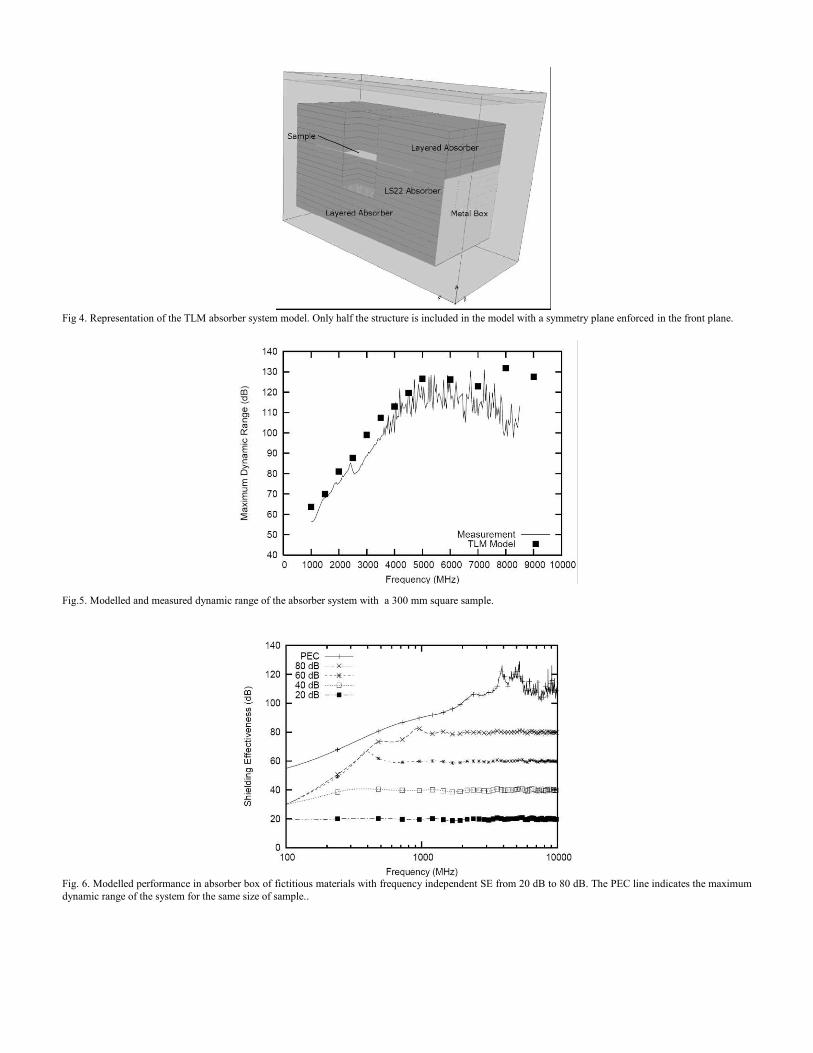
Fig 4. Representation of the TLM absorber system model. Only half the structure is included in the model with a symmetry plane enforced in the front plane.
Fig.5. Modelled and measured dynamic range of the absorber system with a 300 mm square sample.
Fig. 6. Modelled performance in absorber box of fictitious materials with frequency independent SE from 20 dB to 80 dB. The PEC line indicates the maximum
dynamic range of the system for the same size of sample..
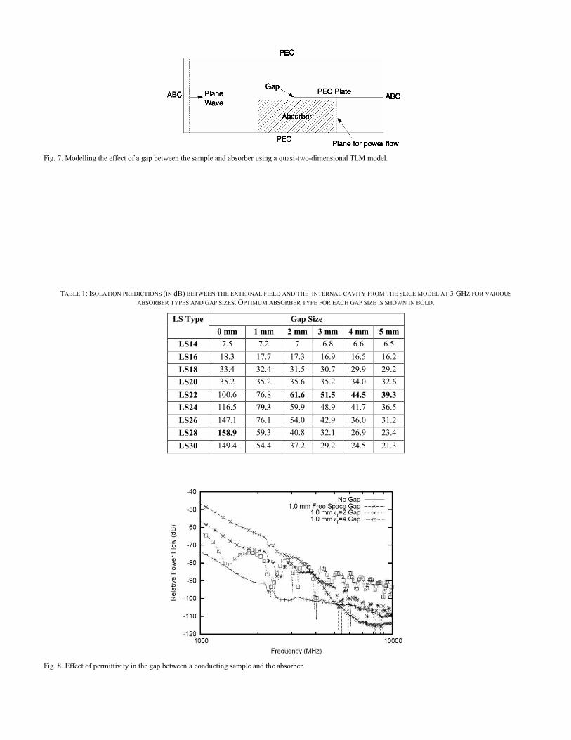
Fig. 7. Modelling the effect of a gap between the sample and absorber using a quasi-two-dimensional TLM model.
TABLE 1: ISOLATION PREDICTIONS (IN dB) BETWEEN THE EXTERNAL FIELD AND THE INTERNAL CAVITY FROM THE SLICE MODEL AT 3 GHZ FOR VARIOUS
ABSORBER TYPES AND GAP SIZES. OPTIMUM ABSORBER TYPE FOR EACH GAP SIZE IS SHOWN IN BOLD.
LS Type Gap Size
0 mm 1 mm 2 mm 3 mm 4 mm 5 mm
LS14 7.5 7.2 7 6.8 6.6 6.5
LS16 18.3 17.7 17.3 16.9 16.5 16.2
LS18 33.4 32.4 31.5 30.7 29.9 29.2
LS20 35.2 35.2 35.6 35.2 34.0 32.6
LS22 100.6 76.8 61.6 51.5 44.5 39.3
LS24 116.5 79.3 59.9 48.9 41.7 36.5
LS26 147.1 76.1 54.0 42.9 36.0 31.2
LS28 158.9 59.3 40.8 32.1 26.9 23.4
LS30 149.4 54.4 37.2 29.2 24.5 21.3
Fig. 8. Effect of permittivity in the gap between a conducting sample and the absorber.
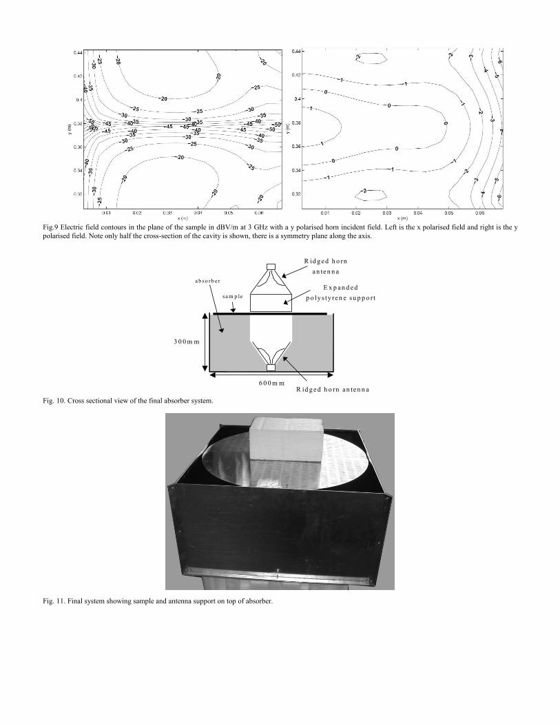
Fig.9 Electric field contours in the plane of the sample in dBV/m at 3 GHz with a y polarised horn incident field. Left is the x polarised field and right is the y
polarised field. Note only half the cross-section of the cavity is shown, there is a symmetry plane along the axis.
6 0 0 m m
3 0 0 m m
R id g e d h o rn
a n te n n a
a b so rb e r
sa m p le
E x p a n d e d
p o ly s ty re n e su p p o rt
R id g e d h o rn a n te n n a
Fig. 10. Cross sectional view of the final absorber system.
Fig. 11. Final system showing sample and antenna support on top of absorber.
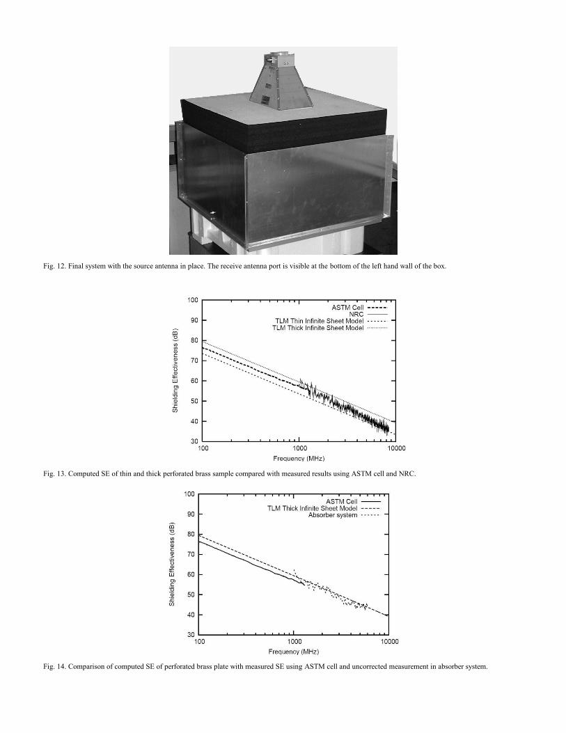
Fig. 12. Final system with the source antenna in place. The receive antenna port is visible at the bottom of the left hand wall of the box.
Fig. 13. Computed SE of thin and thick perforated brass sample compared with measured results using ASTM cell and NRC.
Fig. 14. Comparison of computed SE of perforated brass plate with measured SE using ASTM cell and uncorrected measurement in absorber system.
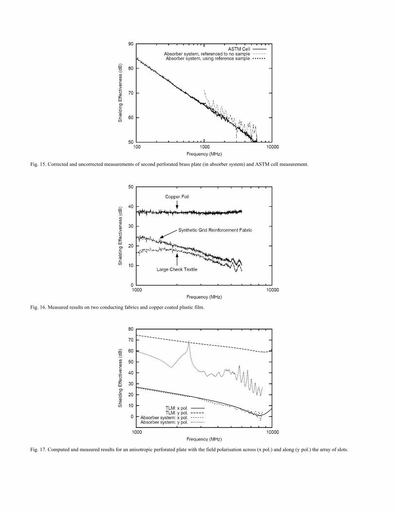
Fig. 15. Corrected and uncorrected measurements of second perforated brass plate (in absorber system) and ASTM cell measurement.
Fig. 16. Measured results on two conducting fabrics and copper coated plastic film.
Fig. 17. Computed and measured results for an anisotropic perforated plate with the field polarisation across (x pol.) and along (y pol.) the array of slots.
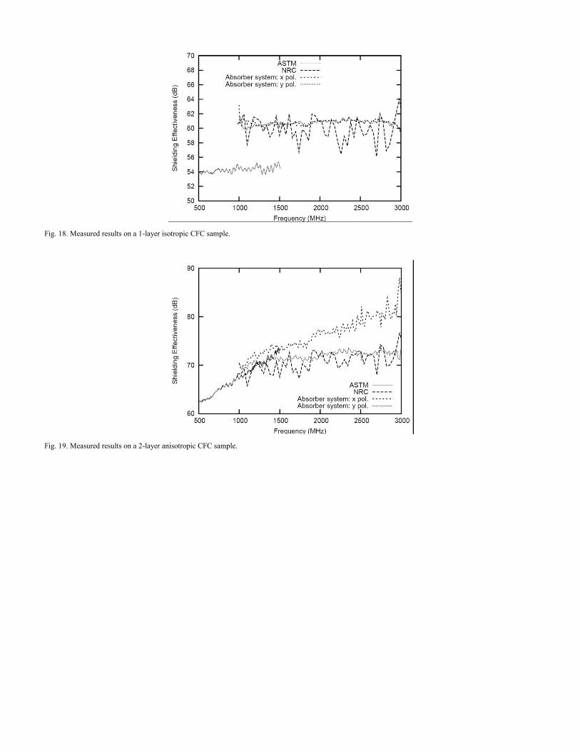
Fig. 18. Measured results on a 1-layer isotropic CFC sample.
Fig. 19. Measured results on a 2-layer anisotropic CFC sample.
Related Documents