Analog Integrated Circuits and Signal Processing, 18, 255–275 (1999) # 1999 Kluwer Academic Publishers, Boston. Manufactured in The Netherlands. A Locally Adaptive Multimode Photodetector Circuit AMJAD KHAN, ANANT DEVAL AND L. A. AKERS Center For Solid State Electronics Research, Department Of Electrical Engineering, Arizona State University, Tempe, AZ 85298-5706 [email protected] Received March 20, 1997; Revised January 13, 1998; Accepted February 9, 1998 Abstract. Photodetection circuits form the first stage of the artificial image acquisition process. The image acquisition circuits discussed in this paper pertain to circuits fabricated in a standard CMOS process. Such circuits offers advantages such as random access to a pixel, faster readout, integration of processing circuitry on the same die, low voltage and low power dissipation, and lower cost over the conventional Charge Coupled Device (CCD) process. We describe a new locally adaptive multimode photodetector circuit. The advantages of the circuit are local adaptation, wide dynamic range, excellent sensitivity, and large output voltage swing. The circuit was fabricated in the 2m CMOS process through MOSIS. Simulation and experimental results of the circuit are given. Key Words: photodetection circuits, CMOS, vision, imagers, CCD, Active Pixel Sensors (APS) 1. Introduction Human vision is an image capture and processing system of enormous complexity comprising the retina, visual cortex, and other interconnected brain systems. It is believed that over 55% of the human cortex is devoted to vision processing. The building of such a system artificially is truly a big challenge. The first step in such a system is the transduction of light into electrons. The circuits used for image acquisition are called photodetection circuits or image sensors. Signals from the photodetector circuits are either directly stored in memory or further processed and stored. The stored data is used to reconstruct the captured image, for example on a computer screen or further processing is done to extract the information contained in the image. The basic technologies used for image acquisition are CCD imagers, and CMOS imagers. While the CCD technology has been dominant till now, CMOS technology offers advantages such as random access to a pixel, faster readout, integration of processing circuitry on the same die, low voltage and low power dissipation, and lower cost over the conventional Charge Coupled Device (CCD) process. Charge coupled devices are special semiconductor devices, fabricated with specialized and costly processes, used for image acquisition. CCD’s sense light intensity by integrating the photocharge in time on a grid of (for example) 860 by 640 pixels. The charge is then shifted out to a register one pixel at a time and read out is destructive. The process is exotic and costly because of the high charge transfer efficiency requirements [1]. The dynamic range of CCD is less compared to the dynamic range of light viewed by humans. When the dynamic range needed to process the image exceeds the CCD’s capability, the image is clipped. Blooming can occur when the charge on a pixel exceeds its holding capacity and spills over into neighboring pixels. In a CCD camera system the photodetector array is on a separate die. The output of the CCD, normally an unconditioned analog signal, is then sent to other chips for additional processing. The output of the CCD camera is NTSC, SECAM or PAL analog output. The main drawback of a CCD process is its high cost to integrate the associated circuitry with the photodetectors on a single chip [1]. CMOS is the standard technology used in making most logic circuits. If CMOS technology is used for imaging then its cost will be less compared to a CCD. In a standard CMOS process various junction diodes, transistors and photogates can be used as photodetecting elements. The associated circuitry easily converts the charge into a voltage or current which can be randomly read from an

Welcome message from author
This document is posted to help you gain knowledge. Please leave a comment to let me know what you think about it! Share it to your friends and learn new things together.
Transcript
Analog Integrated Circuits and Signal Processing, 18, 255±275 (1999)
# 1999 Kluwer Academic Publishers, Boston. Manufactured in The Netherlands.
A Locally Adaptive Multimode Photodetector Circuit
AMJAD KHAN, ANANT DEVAL AND L. A. AKERSCenter For Solid State Electronics Research, Department Of Electrical Engineering, Arizona State University, Tempe, AZ 85298-5706
Received March 20, 1997; Revised January 13, 1998; Accepted February 9, 1998
Abstract. Photodetection circuits form the ®rst stage of the arti®cial image acquisition process. The image
acquisition circuits discussed in this paper pertain to circuits fabricated in a standard CMOS process. Such circuits
offers advantages such as random access to a pixel, faster readout, integration of processing circuitry on the same
die, low voltage and low power dissipation, and lower cost over the conventional Charge Coupled Device (CCD)
process. We describe a new locally adaptive multimode photodetector circuit. The advantages of the circuit are
local adaptation, wide dynamic range, excellent sensitivity, and large output voltage swing. The circuit was
fabricated in the 2m CMOS process through MOSIS. Simulation and experimental results of the circuit are given.
Key Words: photodetection circuits, CMOS, vision, imagers, CCD, Active Pixel Sensors (APS)
1. Introduction
Human vision is an image capture and processing
system of enormous complexity comprising the
retina, visual cortex, and other interconnected brain
systems. It is believed that over 55% of the human
cortex is devoted to vision processing. The building of
such a system arti®cially is truly a big challenge. The
®rst step in such a system is the transduction of light
into electrons. The circuits used for image acquisition
are called photodetection circuits or image sensors.
Signals from the photodetector circuits are either
directly stored in memory or further processed and
stored. The stored data is used to reconstruct the
captured image, for example on a computer screen or
further processing is done to extract the information
contained in the image.
The basic technologies used for image acquisition
are CCD imagers, and CMOS imagers. While the
CCD technology has been dominant till now, CMOS
technology offers advantages such as random access
to a pixel, faster readout, integration of processing
circuitry on the same die, low voltage and low power
dissipation, and lower cost over the conventional
Charge Coupled Device (CCD) process.
Charge coupled devices are special semiconductor
devices, fabricated with specialized and costly
processes, used for image acquisition. CCD's sense
light intensity by integrating the photocharge in time
on a grid of (for example) 860 by 640 pixels. The
charge is then shifted out to a register one pixel at a
time and read out is destructive. The process is exotic
and costly because of the high charge transfer
ef®ciency requirements [1]. The dynamic range of
CCD is less compared to the dynamic range of light
viewed by humans. When the dynamic range needed
to process the image exceeds the CCD's capability,
the image is clipped. Blooming can occur when the
charge on a pixel exceeds its holding capacity and
spills over into neighboring pixels. In a CCD camera
system the photodetector array is on a separate die.
The output of the CCD, normally an unconditioned
analog signal, is then sent to other chips for additional
processing. The output of the CCD camera is NTSC,
SECAM or PAL analog output. The main drawback of
a CCD process is its high cost to integrate the
associated circuitry with the photodetectors on a
single chip [1].
CMOS is the standard technology used in making
most logic circuits. If CMOS technology is used
for imaging then its cost will be less compared to a
CCD. In a standard CMOS process various
junction diodes, transistors and photogates can be
used as photodetecting elements. The associated
circuitry easily converts the charge into a voltage
or current which can be randomly read from an
array of pixels like a DRAM, unlike a CCD system.
There are also some disadvantages. Disadvantages are
®xed pattern noise, less ®ll factor compared to a CCD,
blooming, lag, and effects of noise due to digital
switching of the associated circuitry. The most
popular type of photodetection circuits which in-
clude gain in the pixel are called Active Pixel
Sensors (APS).
The applications for these kind of sensors are in
digital cameras, multimedia applications, and in other
portable vision systems. With the trend towards
replacing CCD devices with CMOS, there is a
demand for new and enhanced photodetecting circuits
and optimum pixel architectures. These circuits are
critical to a design of a CMOS imager.
We describe a new type of photodetection circuit
called a Locally Adaptive Multimode Photodetector
Circuit, which has a better sensitivity and increased
dynamic range compared to standard photodetectors.
The circuit will optimize the tradeoff between the
dynamic range and sensitivity of the CMOS imagers.
The operation of this kind of circuit is based on the
principle of automatically adjusting the gain of the
circuit such that it adapts to locally changing light
intensity.
2. Photodetection Circuits
The light intensity present in the environment varies
about 14 orders of magnitude [2] with the brightest
intensity corresponding to noon sunlight in June
(1 W/cm2) and the darkest corresponding to night sky
illumination (10ÿ 14 W/cm2). The full moon light
corresponds to approximately 10ÿ 6 W/cm2. The main
challenge in designing a CMOS imager is to operate it
over a wide dynamic range of light just like a human
eye. Circuits are needed to detect light intensity over a
wide range of interest which can be 7±10 decades if
not the complete 14 decades. Present CMOS sensors
have a dynamic range of 6±7 orders of magnitude [3],
with a tradeoff between dynamic range and sensi-
tivity. If you have large dynamic range then the
sensitivity will be low and vice versa. In imaging
systems which operate at 5 V, the least voltage which
can be detected accurately with an 8 bit A/D converter
is about 20 mV. Seven decades of photocurrent
requires a resolution of 500 nV. Gaining such a
sensitivity by increasing the number of bits in an
A/D is not practical since data handling would make
the system complex and it is also dif®cult to store such
small voltages on the gate capacitors so that they can
be sampled at a later time.
Detecting the light intensity and converting it
into an electrical parameter (voltage or current), and
subsequently processing the signals from an array of
detectors, in spatial and/or temporal domain, are the
primary tasks of vision chips. It is very important to
understand the physics behind the devices used in
transduction of light as these devices play a critical
role in design of photodetection circuits. The
characteristics of the detectors, such as dynamic
range, spectral ef®ciency, noise, linearity, band-
width, etc. directly affect the performance of the
system.
A pn junction photodiode is just a pn junction
diode which is fabricated such that light can fall on its
metallurgical junction. The absorption of light inside
the diode creates electron-hole pairs. On average,
minority carriers created within a diffusion length in
the quasineutral regions diffuse to the depletion
region. These carriers, and carriers photogenerated
within the depletion region, are subsequently swept by
the E-®eld to the opposite side of the junction, thereby
contributing an added reverse current through the
diode.
The junction photodiodes have a linear behavior
over a dynamic range of more than 7 decade [4], with
reasonable sensitivity to the visible light spectrum. In
a standard CMOS process, either p-well or n-well,
several parasitic junction devices are possible for
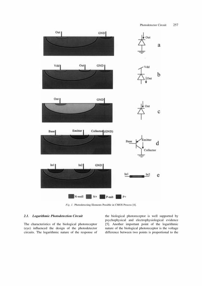
photodetection. Fig. 1 gives a pictorial representation
of the various junction diodes possible. The ®rst three
structures are junction diodes, the fourth one is a
parasitic vertical bipolar transistor, and the last
structure is capable of bi-directional photocurrent
generation depending on the voltage across the
device. The last structure can be considered as a
lateral bipolar transistor with symmetric emitter and
collector which depends on the separation between
the two diffusion areas. All of the photodetecting
elements respond acceptably in the visual light range
with slight differences depending on the depth of the
junctio [4].
The photodetection circuits that are most often
used are:* Logarithmic Photodetection Circuit* Active Pixel Sensor* Adaptive Photoreceptor Circuit* Current mode CMOS Imager.
2.1. Logarithmic Photodetection Circuit
The characteristics of the biological photoreceptor
(eye) in¯uenced the design of the photodetector
circuits. The logarithmic nature of the response of
the biological photoreceptor is well supported by
psychophysical and electrophysiological evidence
[5]. Another important point of the logarithmic
nature of the biological photoreceptor is the voltage
difference between two points is proportional to the
Fig. 1. Photodetecting Elements Possible in CMOS Process [4].
Photodetector Circuit 257
contrast ratio between the two corresponding points in
the image [5]. The contrast ratio is de®ned as the ratio
between the re¯ectance of two adjacent objects,
re¯ectance which are independent of the illumination
level. The logarithmic photodetector circuit is one
which transduces light into a DC level which is
proportional to the logarithm of the input photo-
current. Thus a wide dynamic range of light is
converted into a small range of output voltage. The
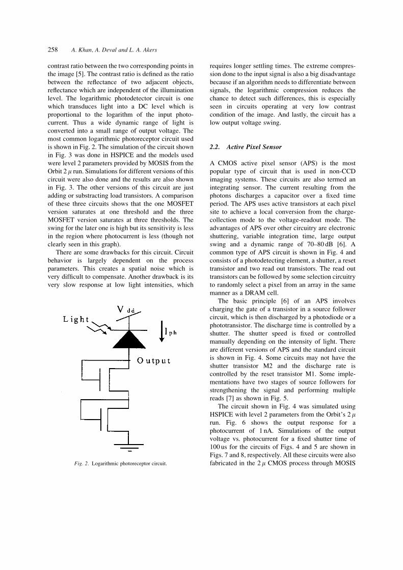
most common logarithmic photoreceptor circuit used
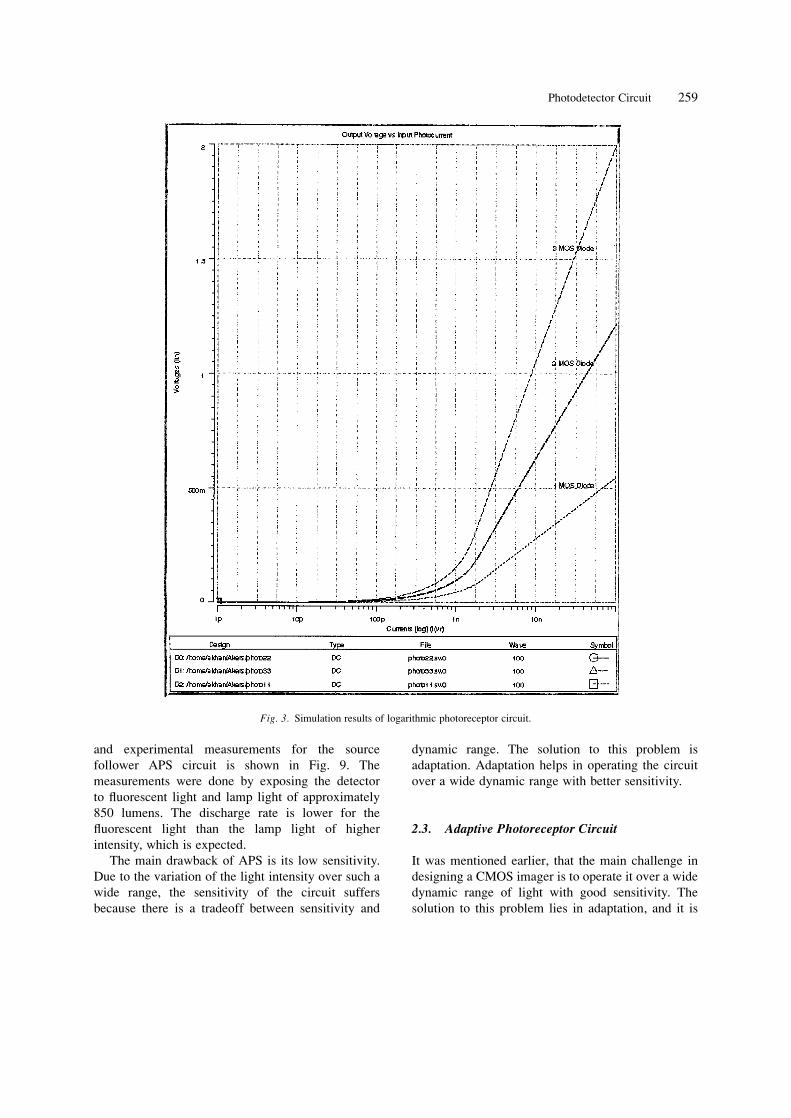
is shown in Fig. 2. The simulation of the circuit shown
in Fig. 3 was done in HSPICE and the models used
were level 2 parameters provided by MOSIS from the
Orbit 2 m run. Simulations for different versions of this
circuit were also done and the results are also shown
in Fig. 3. The other versions of this circuit are just
adding or substracting load transistors. A comparison
of these three circuits shows that the one MOSFET
version saturates at one threshold and the three
MOSFET version saturates at three thresholds. The
swing for the later one is high but its sensitivity is less
in the region where photocurrent is less (though not
clearly seen in this graph).
There are some drawbacks for this circuit. Circuit
behavior is largely dependent on the process
parameters. This creates a spatial noise which is
very dif®cult to compensate. Another drawback is its
very slow response at low light intensities, which
requires longer settling times. The extreme compres-
sion done to the input signal is also a big disadvantage
because if an algorithm needs to differentiate between
signals, the logarithmic compression reduces the
chance to detect such differences, this is especially
seen in circuits operating at very low contrast
condition of the image. And lastly, the circuit has a
low output voltage swing.
2.2. Active Pixel Sensor
A CMOS active pixel sensor (APS) is the most
popular type of circuit that is used in non-CCD
imaging systems. These circuits are also termed an
integrating sensor. The current resulting from the
photons discharges a capacitor over a ®xed time
period. The APS uses active transistors at each pixel
site to achieve a local conversion from the charge-
collection mode to the voltage-readout mode. The
advantages of APS over other circuitry are electronic
shuttering, variable integration time, large output
swing and a dynamic range of 70±80 dB [6]. A
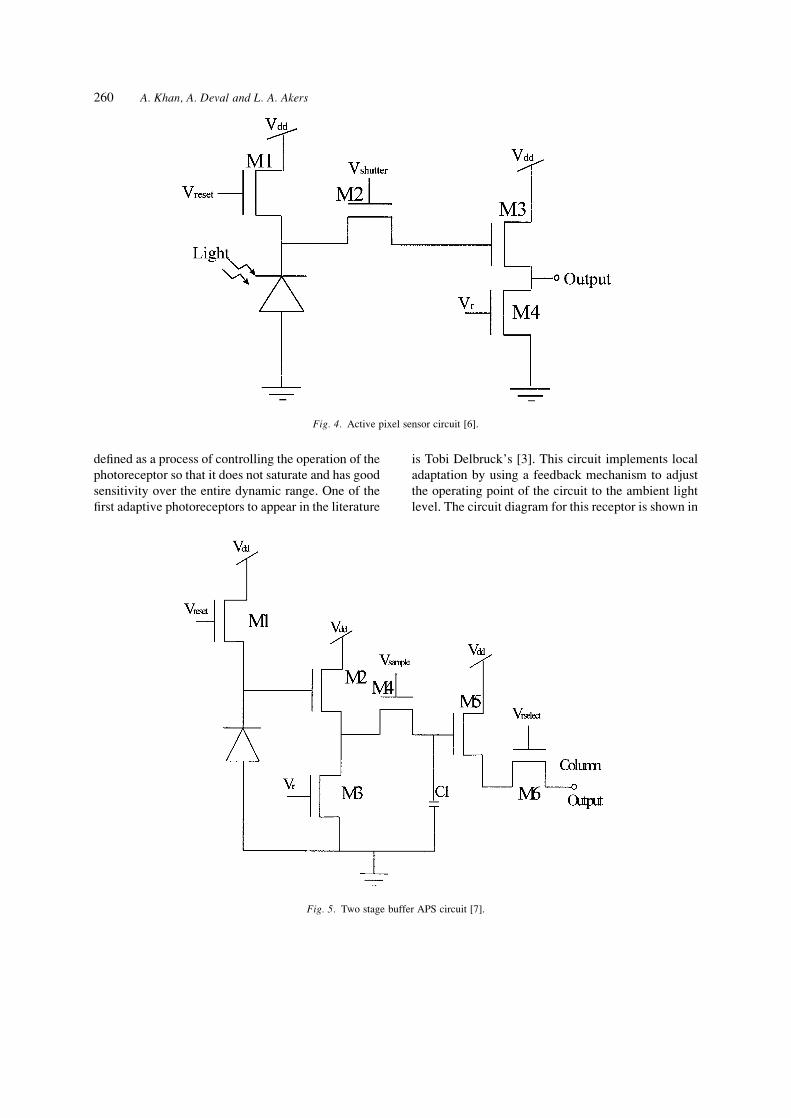
common type of APS circuit is shown in Fig. 4 and
consists of a photodetecting element, a shutter, a reset
transistor and two read out transistors. The read out
transistors can be followed by some selection circuitry
to randomly select a pixel from an array in the same
manner as a DRAM cell.
The basic principle [6] of an APS involves
charging the gate of a transistor in a source follower
circuit, which is then discharged by a photodiode or a
phototransistor. The discharge time is controlled by a
shutter. The shutter speed is ®xed or controlled
manually depending on the intensity of light. There
are different versions of APS and the standard circuit
is shown in Fig. 4. Some circuits may not have the
shutter transistor M2 and the discharge rate is
controlled by the reset transistor M1. Some imple-
mentations have two stages of source followers for
strengthening the signal and performing multiple
reads [7] as shown in Fig. 5.
The circuit shown in Fig. 4 was simulated using
HSPICE with level 2 parameters from the Orbit's 2 mrun. Fig. 6 shows the output response for a
photocurrent of 1 nA. Simulations of the output
voltage vs. photocurrent for a ®xed shutter time of
100 us for the circuits of Figs. 4 and 5 are shown in
Figs. 7 and 8, respectively. All these circuits were also
fabricated in the 2 m CMOS process through MOSISFig. 2. Logarithmic photoreceptor circuit.
258 A. Khan, A. Deval and L. A. Akers
and experimental measurements for the source
follower APS circuit is shown in Fig. 9. The
measurements were done by exposing the detector
to ¯uorescent light and lamp light of approximately
850 lumens. The discharge rate is lower for the
¯uorescent light than the lamp light of higher
intensity, which is expected.
The main drawback of APS is its low sensitivity.
Due to the variation of the light intensity over such a
wide range, the sensitivity of the circuit suffers
because there is a tradeoff between sensitivity and
dynamic range. The solution to this problem is
adaptation. Adaptation helps in operating the circuit
over a wide dynamic range with better sensitivity.
2.3. Adaptive Photoreceptor Circuit
It was mentioned earlier, that the main challenge in
designing a CMOS imager is to operate it over a wide
dynamic range of light with good sensitivity. The
solution to this problem lies in adaptation, and it is
Fig. 3. Simulation results of logarithmic photoreceptor circuit.
Photodetector Circuit 259
de®ned as a process of controlling the operation of the
photoreceptor so that it does not saturate and has good
sensitivity over the entire dynamic range. One of the
®rst adaptive photoreceptors to appear in the literature
is Tobi Delbruck's [3]. This circuit implements local
adaptation by using a feedback mechanism to adjust
the operating point of the circuit to the ambient light
level. The circuit diagram for this receptor is shown in
Fig. 4. Active pixel sensor circuit [6].
Fig. 5. Two stage buffer APS circuit [7].
260 A. Khan, A. Deval and L. A. Akers
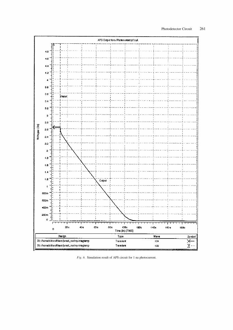
Fig. 6. Simulation result of APS circuit for 1 na photocurrent.
Photodetector Circuit 261
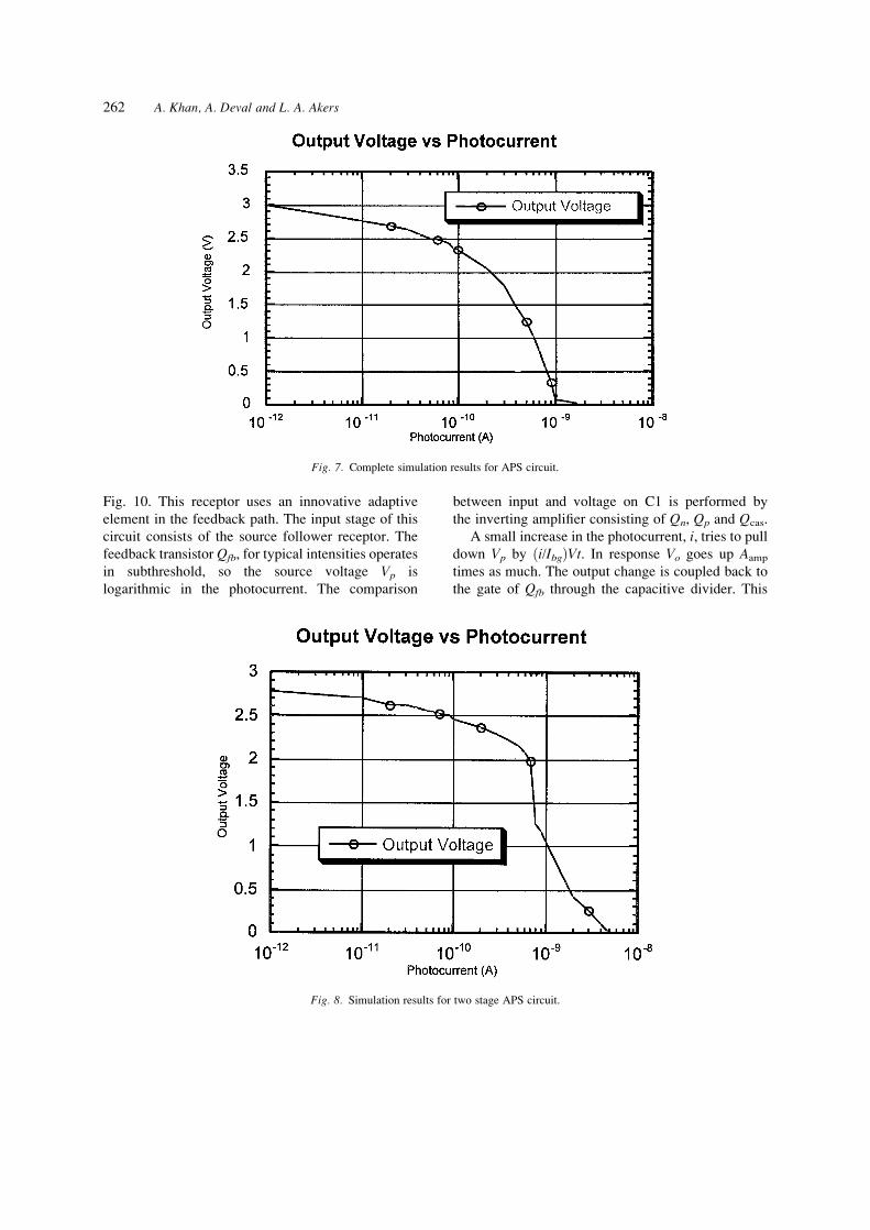
Fig. 10. This receptor uses an innovative adaptive
element in the feedback path. The input stage of this
circuit consists of the source follower receptor. The
feedback transistor Qfb, for typical intensities operates
in subthreshold, so the source voltage Vp is
logarithmic in the photocurrent. The comparison
between input and voltage on C1 is performed by
the inverting ampli®er consisting of Qn, Qp and Qcas.
A small increase in the photocurrent, i, tries to pull
down Vp by �i/Ibg�Vt. In response Vo goes up Aamp
times as much. The output change is coupled back to
the gate of Qfb through the capacitive divider. This
Fig. 7. Complete simulation results for APS circuit.
Fig. 8. Simulation results for two stage APS circuit.
262 A. Khan, A. Deval and L. A. Akers
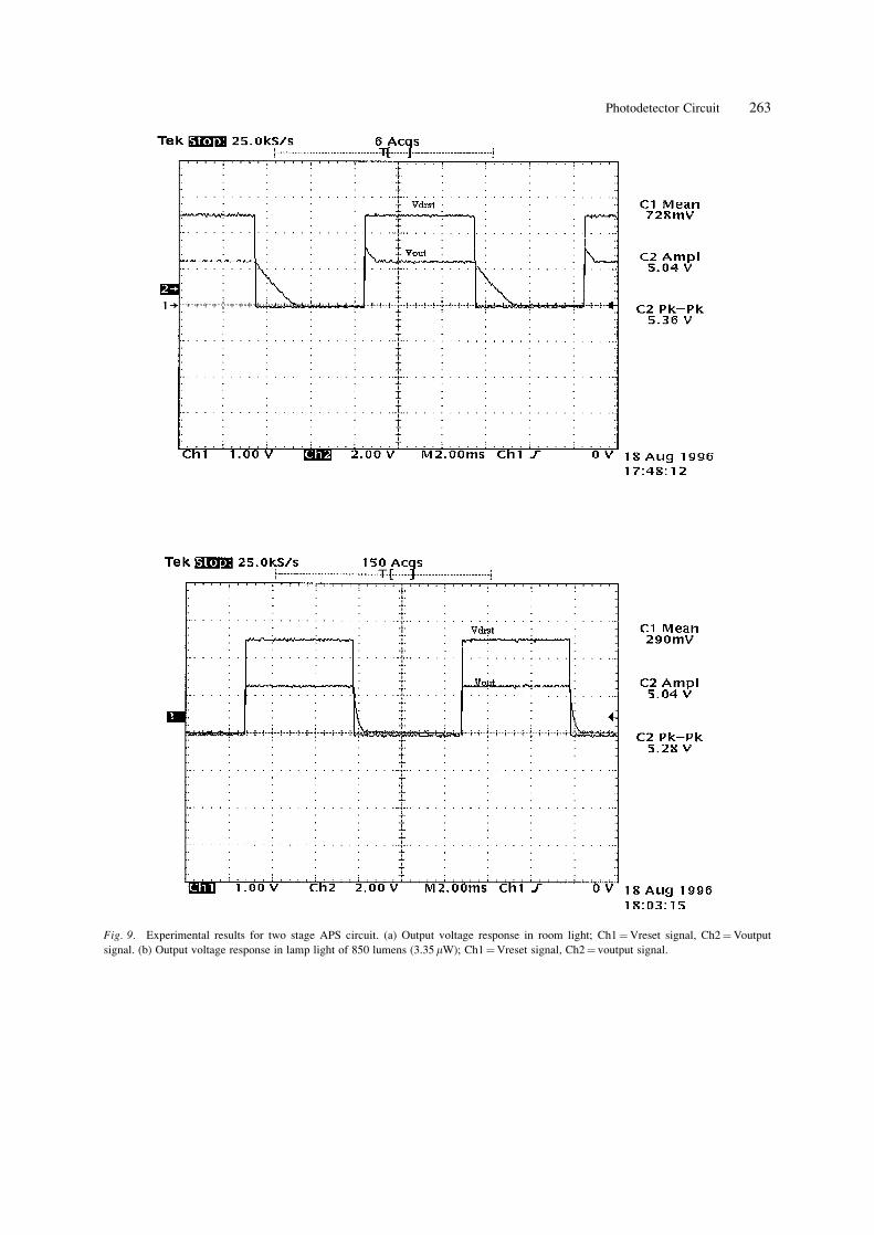
Fig. 9. Experimental results for two stage APS circuit. (a) Output voltage response in room light; Ch1�Vreset signal, Ch2�Voutput
signal. (b) Output voltage response in lamp light of 850 lumens (3.35mW); Ch1�Vreset signal, Ch2� voutput signal.
Photodetector Circuit 263
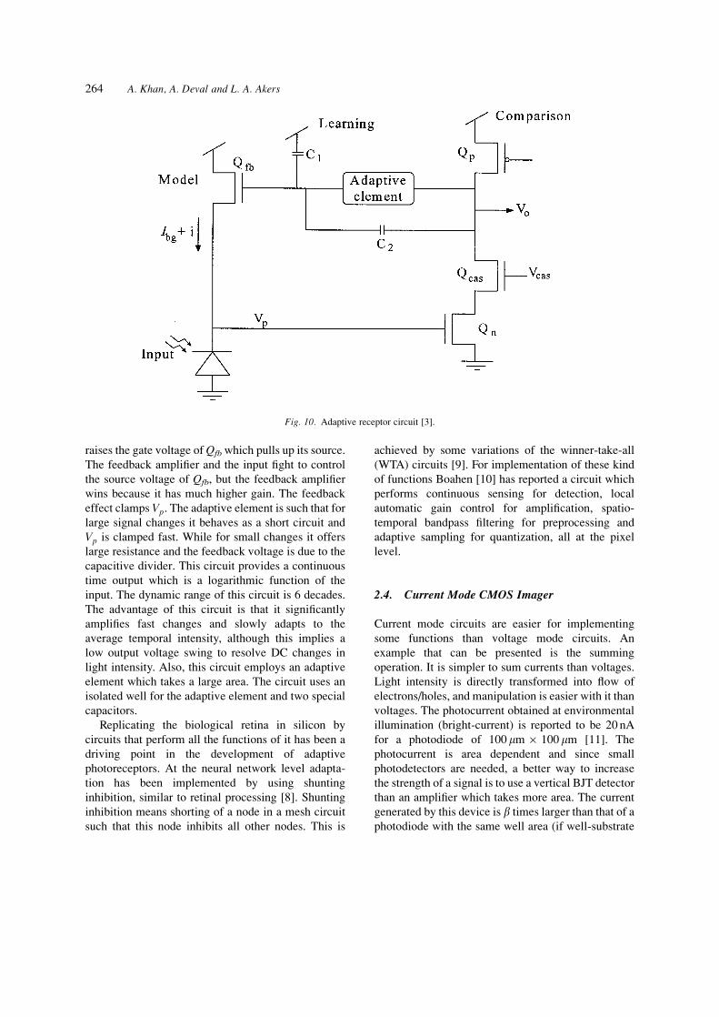
raises the gate voltage of Qfb which pulls up its source.
The feedback ampli®er and the input ®ght to control
the source voltage of Qfb, but the feedback ampli®er
wins because it has much higher gain. The feedback
effect clamps Vp. The adaptive element is such that for
large signal changes it behaves as a short circuit and
Vp is clamped fast. While for small changes it offers
large resistance and the feedback voltage is due to the
capacitive divider. This circuit provides a continuous
time output which is a logarithmic function of the
input. The dynamic range of this circuit is 6 decades.
The advantage of this circuit is that it signi®cantly
ampli®es fast changes and slowly adapts to the
average temporal intensity, although this implies a
low output voltage swing to resolve DC changes in
light intensity. Also, this circuit employs an adaptive
element which takes a large area. The circuit uses an
isolated well for the adaptive element and two special
capacitors.
Replicating the biological retina in silicon by
circuits that perform all the functions of it has been a
driving point in the development of adaptive
photoreceptors. At the neural network level adapta-
tion has been implemented by using shunting
inhibition, similar to retinal processing [8]. Shunting
inhibition means shorting of a node in a mesh circuit
such that this node inhibits all other nodes. This is
achieved by some variations of the winner-take-all
(WTA) circuits [9]. For implementation of these kind
of functions Boahen [10] has reported a circuit which
performs continuous sensing for detection, local
automatic gain control for ampli®cation, spatio-
temporal bandpass ®ltering for preprocessing and
adaptive sampling for quantization, all at the pixel
level.
2.4. Current Mode CMOS Imager
Current mode circuits are easier for implementing
some functions than voltage mode circuits. An
example that can be presented is the summing
operation. It is simpler to sum currents than voltages.
Light intensity is directly transformed into ¯ow of
electrons/holes, and manipulation is easier with it than
voltages. The photocurrent obtained at environmental
illumination (bright-current) is reported to be 20 nA
for a photodiode of 100 mm6 100 mm [11]. The
photocurrent is area dependent and since small
photodetectors are needed, a better way to increase
the strength of a signal is to use a vertical BJT detector
than an ampli®er which takes more area. The current
generated by this device is b times larger than that of a
photodiode with the same well area (if well-substrate
Fig. 10. Adaptive receptor circuit [3].
264 A. Khan, A. Deval and L. A. Akers
photodiode was used). To further strengthen the signal
a Darlington pair can also be used.
A current mode photodetector based on the notion
discussed in the previous paragraph is shown in Fig.
11. This sensor gives a output which is proportional to
the difference between two currents. If the concept of
local adaptation is applied the current can be the
average photocurrent from a group of close pixels.
The output is proportional to the difference between
absolute light intensity and average light intensity.
This signal can be further processed to implement
edge and bar detection functions. The main advantage
of this kind of circuit is its good signal strength and
easy processing capabilities. The disadvantage of this
circuitry is due to its gain of b it ampli®es dark current
also. If a Darlington pair is used then the dark current
ampli®cation is b2.
2.5. Need for a New Circuit
The main idea that is obtained from the previous
section is that an ideal photodetector is one that should
have large dynamic range, high sensitivity, low noise,
less dark current and most importantly it should be
adaptive to the changing light intensity. The adapta-
tion should be local and not global. Our idea is not to
mimic the biological vision systems. The main aim
was to develop an active pixel sensor circuit which did
not compromize sensitivity for dynamic range. If the
active pixel sensor could respond to the variation in
light intensity by changing its gain, in other words the
APS could adapt to the light intensity, then it would
have better dynamic range and sensitivity.
3. Locally Adaptive Multimode Photodetector
We present a circuit that is an active pixel sensor, is
locally adaptive and operated with more than one
level of gain automatically determined by the local
light level. The notion of this circuit is based on the
CMOS photodetector proposed by Ward et. al [2].
However, Ward's circuit did not contain the circuitry
to automatically switch the gain depending on the
local light level. The photodetectors presented till
Fig. 11. Current mode photodetector circuit [2].
Photodetector Circuit 265
now used a photodiode or phototransistor, both
featuring a single mode of operation. A drawback
with photodiode is that it is relatively insensitive to
light with less intensity, and consequently large areas
are required. A phototransistor can be implemented in
approximately the same area (compared to a well-
substrate photodiode) which is more sensitive to
detect an optical signal that is weak [2]. However, the
drawback with this approach is it consumes more
power and ampli®es the dark current. A detector that
can combine the good qualities of both is one that can
be operated as a phototransistor for low light levels
and then as a photodiode in higher light levels The
main idea behind this photodetector is to divide the
range of light intensity into two regions and operate
the circuit in these two regions. The sensitivity of the
detector increases by operating the detector circuit in
these two modes. The output of this photodetector
circuit is the output voltage and the region of
operation.
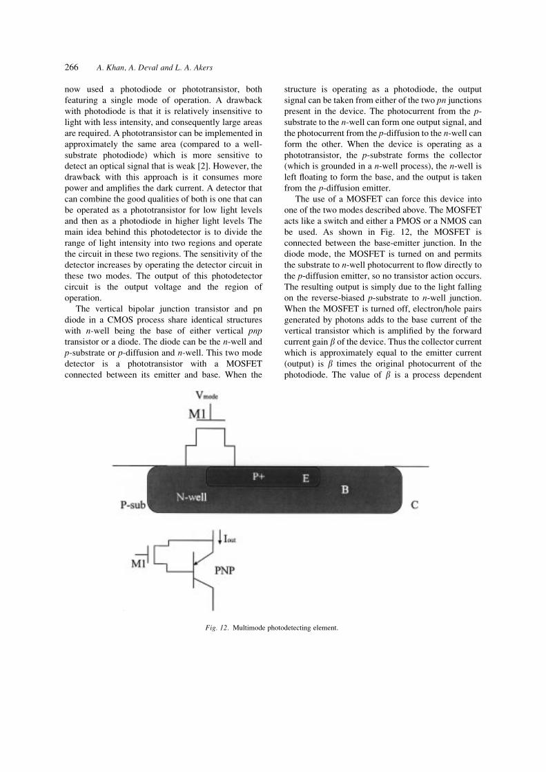
The vertical bipolar junction transistor and pn
diode in a CMOS process share identical structures
with n-well being the base of either vertical pnptransistor or a diode. The diode can be the n-well and
p-substrate or p-diffusion and n-well. This two mode
detector is a phototransistor with a MOSFET
connected between its emitter and base. When the
structure is operating as a photodiode, the output
signal can be taken from either of the two pn junctions
present in the device. The photocurrent from the p-
substrate to the n-well can form one output signal, and
the photocurrent from the p-diffusion to the n-well can
form the other. When the device is operating as a
phototransistor, the p-substrate forms the collector
(which is grounded in a n-well process), the n-well is
left ¯oating to form the base, and the output is taken
from the p-diffusion emitter.
The use of a MOSFET can force this device into
one of the two modes described above. The MOSFET
acts like a switch and either a PMOS or a NMOS can
be used. As shown in Fig. 12, the MOSFET is
connected between the base-emitter junction. In the
diode mode, the MOSFET is turned on and permits
the substrate to n-well photocurrent to ¯ow directly to
the p-diffusion emitter, so no transistor action occurs.
The resulting output is simply due to the light falling
on the reverse-biased p-substrate to n-well junction.
When the MOSFET is turned off, electron/hole pairs
generated by photons adds to the base current of the
vertical transistor which is ampli®ed by the forward
current gain b of the device. Thus the collector current
which is approximately equal to the emitter current
(output) is b times the original photocurrent of the
photodiode. The value of b is a process dependent
Fig. 12. Multimode photodetecting element.
266 A. Khan, A. Deval and L. A. Akers
parameter and varies from 10±100 [13]. Further
modes can be achieved with two transistors connected
as a Darlington pair and with the use of MOSFET
switches they can be switched into different modes
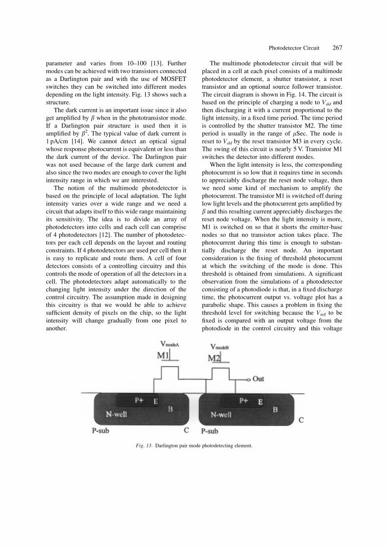
depending on the light intensity. Fig. 13 shows such a
structure.
The dark current is an important issue since it also
get ampli®ed by b when in the phototransistor mode.
If a Darlington pair structure is used then it is
ampli®ed by b2. The typical value of dark current is
1 pA/cm [14]. We cannot detect an optical signal
whose response photocurrent is equivalent or less than
the dark current of the device. The Darlington pair
was not used because of the large dark current and
also since the two modes are enough to cover the light
intensity range in which we are interested.
The notion of the multimode photodetector is
based on the principle of local adaptation. The light
intensity varies over a wide range and we need a
circuit that adapts itself to this wide range maintaining
its sensitivity. The idea is to divide an array of
photodetectors into cells and each cell can comprise
of 4 photodetectors [12]. The number of photodetec-
tors per each cell depends on the layout and routing
constraints. If 4 photodetectors are used per cell then it
is easy to replicate and route them. A cell of four
detectors consists of a controlling circuitry and this
controls the mode of operation of all the detectors in a
cell. The photodetectors adapt automatically to the
changing light intensity under the direction of the
control circuitry. The assumption made in designing
this circuitry is that we would be able to achieve
suf®cient density of pixels on the chip, so the light
intensity will change gradually from one pixel to
another.
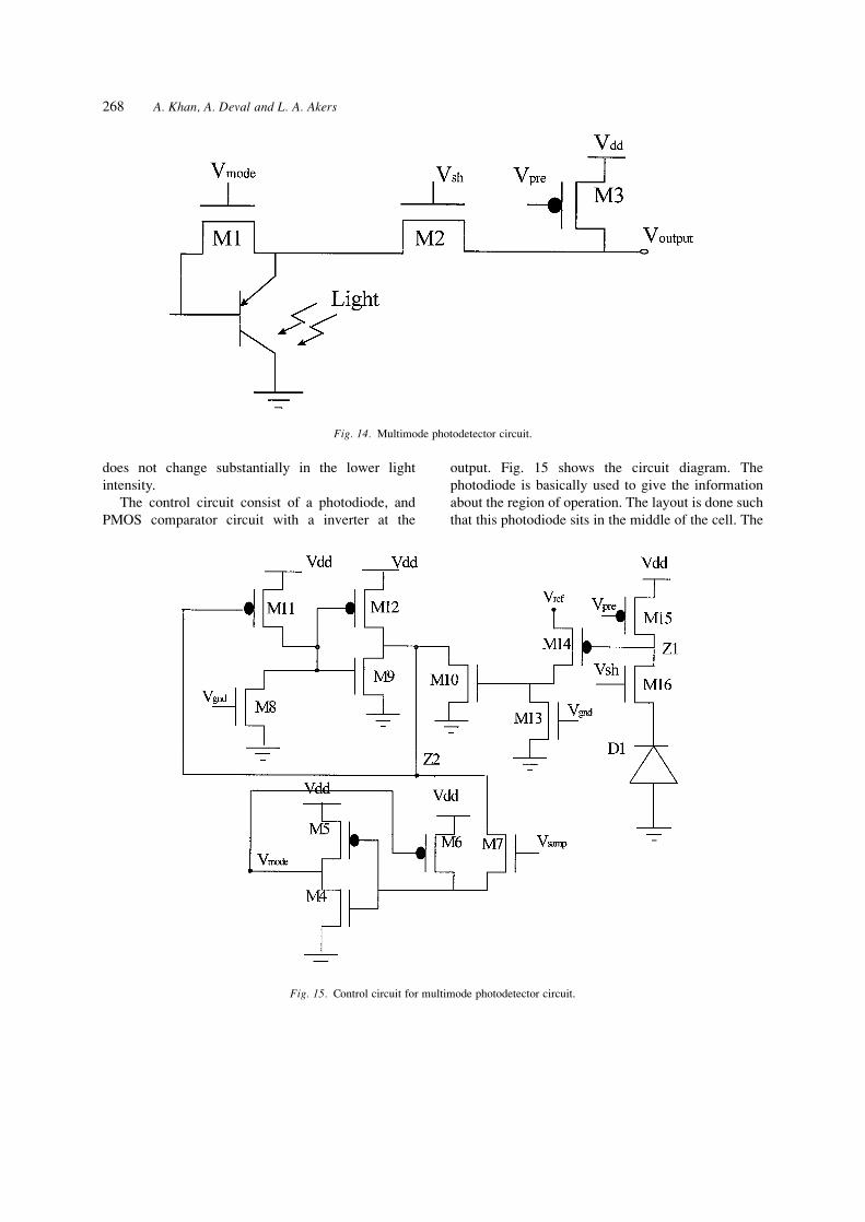
The multimode photodetector circuit that will be
placed in a cell at each pixel consists of a multimode
photodetector element, a shutter transistor, a reset
transistor and an optional source follower transistor.
The circuit diagram is shown in Fig. 14. The circuit is
based on the principle of charging a node to Vdd and
then discharging it with a current proportional to the
light intensity, in a ®xed time period. The time period
is controlled by the shutter transistor M2. The time
period is usually in the range of mSec. The node is
reset to Vdd by the reset transistor M3 in every cycle.
The swing of this circuit is nearly 5 V. Transistor M1
switches the detector into different modes.
When the light intensity is less, the corresponding
photocurrent is so low that it requires time in seconds
to appreciably discharge the reset node voltage, then
we need some kind of mechanism to amplify the
photocurrent. The transistor M1 is switched off during
low light levels and the photocurrent gets ampli®ed by
b and this resulting current appreciably discharges the
reset node voltage. When the light intensity is more,
M1 is switched on so that it shorts the emitter-base
nodes so that no transistor action takes place. The
photocurrent during this time is enough to substan-
tially discharge the reset node. An important
consideration is the ®xing of threshold photocurrent
at which the switching of the mode is done. This
threshold is obtained from simulations. A signi®cant
observation from the simulations of a photodetector
consisting of a photodiode is that, in a ®xed discharge
time, the photocurrent output vs. voltage plot has a
parabolic shape. This causes a problem in ®xing the
threshold level for switching because the Vref to be
®xed is compared with an output voltage from the
photodiode in the control circuitry and this voltage
Fig. 13. Darlington pair mode photodetecting element.
Photodetector Circuit 267
does not change substantially in the lower light
intensity.
The control circuit consist of a photodiode, and
PMOS comparator circuit with a inverter at the
output. Fig. 15 shows the circuit diagram. The
photodiode is basically used to give the information
about the region of operation. The layout is done such
that this photodiode sits in the middle of the cell. The
Fig. 14. Multimode photodetector circuit.
Fig. 15. Control circuit for multimode photodetector circuit.
268 A. Khan, A. Deval and L. A. Akers
assumption made is that the light falling on this diode
is approximately the same as that falling on all the
four pixels and the photocurrent obtained from this is
the average photocurrent of the cell. The output of the
photodiode (node Z1) is given to a comparator that
compares the voltage corresponding to the average
photocurrent, to a ®xed reference voltage �Vref�. If the
voltage obtained is less than VrefÿVth then transistor
M14 switches on resulting in the switching on of
transistor M10 also. When M10 turns on node Z2 goes
to ``0'' and this value is sampled to the inverter whose
output will be 1. The output of the inverter is given to
the transistor M1 of Fig. 14.
The ``1'' indicates that the light intensity is in the
brighter region and the multimode photodetector
should operate in the diode mode. The diode mode
is selected by turning on the M1. If the light intensity
is less and the voltage at Z1 is greater than Vref then
M14 remains off and the node Z2 is high due to the
precharge signals Vgnd. When this high is sampled to
the inverter then the gate voltage of M1 (Vmode) is 0
signifying the BJT mode. The multimode photo-
detector is operated in two modes, diode mode and
transistor mode. Transistor M1 controls the mode of
the circuit, depending on the light intensity. If
Vmode� 1 then it operates in the diode mode,
Vmode� 0 corresponds to the BJT mode. The timing
of the input control signals is shown in Fig. 16. The
mode selection is done automatically, and the output
of the pixel is a 1 bit Vmode signal and the value of
Voutput which can be encoded in 7 bits. Thus the output
can be encoded into an 8 bit signal.
The circuit was simulated with HSPICE using the
Orbit's 2 m CMOS process parameters. For simulation
the value of photocurrent was substituted in place of
the reverse current Is in a BJT .MODEL parameters.
Using the timing shown in Fig. 16, simulation results
of the circuit are shown in Fig. 17. The circuit starts in
the BJT mode and as the photocurrent is increased,
after some point (500 pa), it shifts into the diode
mode. The point at which the switch from BJT mode
to diode mode, takes place is determined by the
voltage Vref and shutter time Tsh which were ®xed
with simulation.
4. Experimental Results
The circuit was designed and fabricated in the 2 mm
CMOS process through MOSIS. Fig. 18 gives the
experimental results of this circuit. In these ®gures
CH1 is the precharge signal, CH2 is the shutter pulse
and CH3 is the output voltage. The output was veri®ed
for three different light levels and the results are as
expected from the simulation graphs. Fig. 18(a) gives
the output voltage discharge in the diode mode for the
lamp light. When this is compared with Fig. 18(b),
which give the response of the detector in the BJT
mode for the same light level, it can be seen that
discharge rate is more for the BJT mode than the
diode mode. The three different light sources were the
light of approximately 850 lumens from a 100 W bulb,
room light and darkness of the lab. In the darkness we
get to see the effect of the dark current Figs. 18(c) and
(d) show the diode and BJT circuits at room light with
a shutter speed of 10 us. Again, as expected the BJT
circuit discharges faster. The effect of dark current is
shown in Figs. 18(e) and (f ).
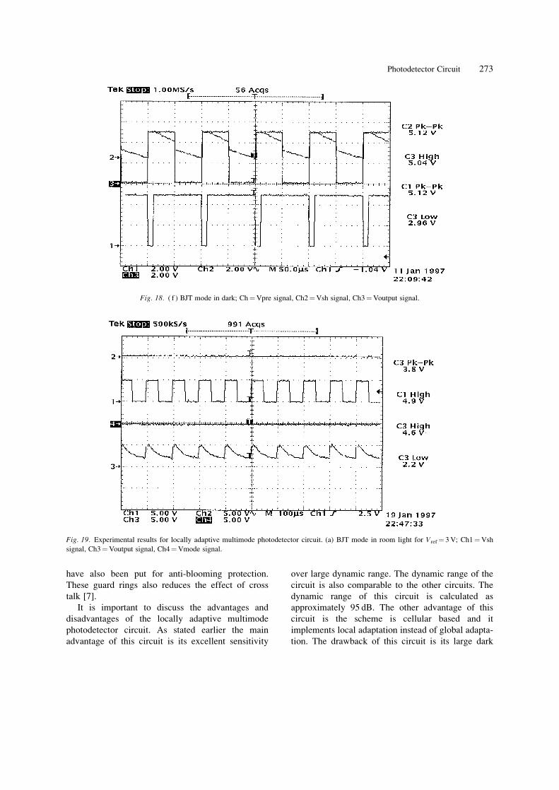
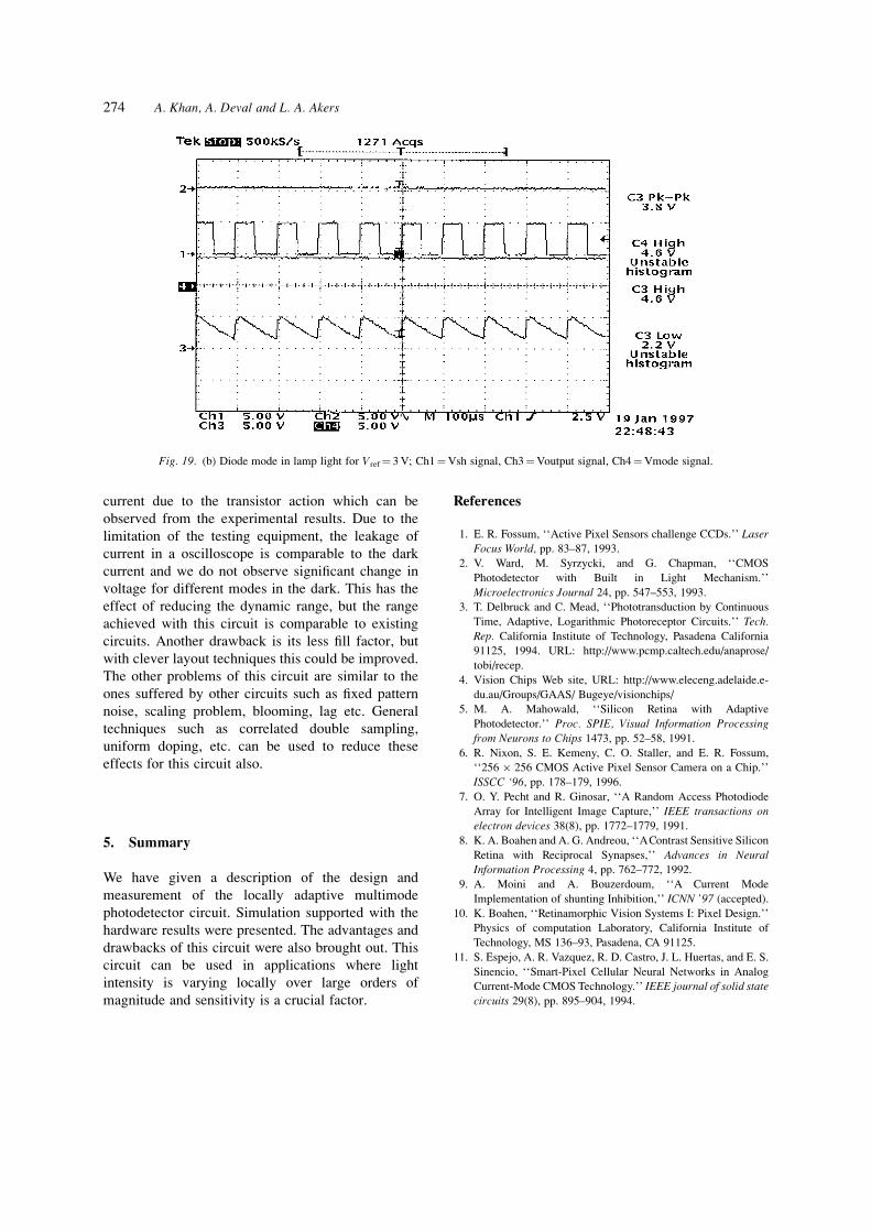
Fig. 19 gives the experimental results for changing
light conditions. The important observation from
these ®gures is that the mode (CH4) changes from
0?1 automatically with an increase in light intensity.
Fig. 19(a) gives the output voltage response (CH3) for
BJT mode since the light intensity is due to room light
only. When the intensity is increased by turning on the
lamp, the circuit shifts automatically into the diode
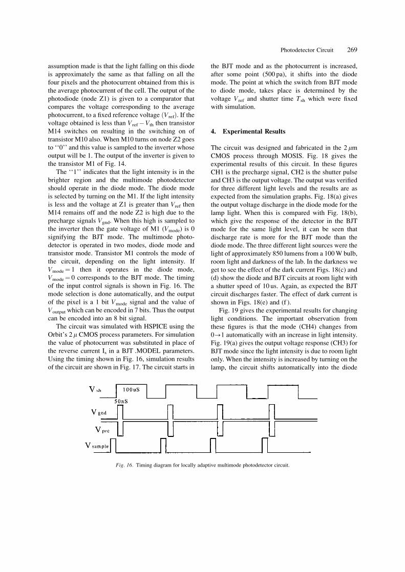
Fig. 16. Timing diagram for locally adaptive multimode photodetector circuit.
Photodetector Circuit 269
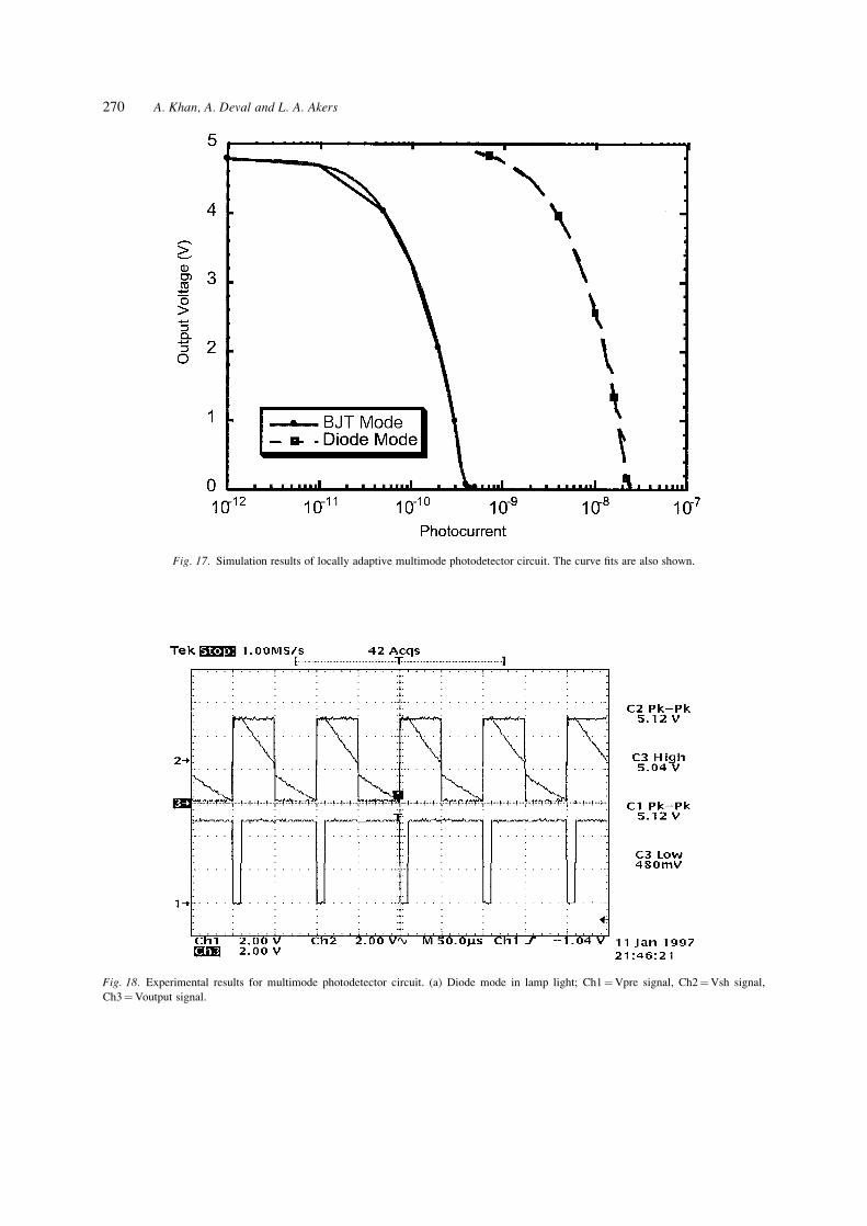
Fig. 17. Simulation results of locally adaptive multimode photodetector circuit. The curve ®ts are also shown.
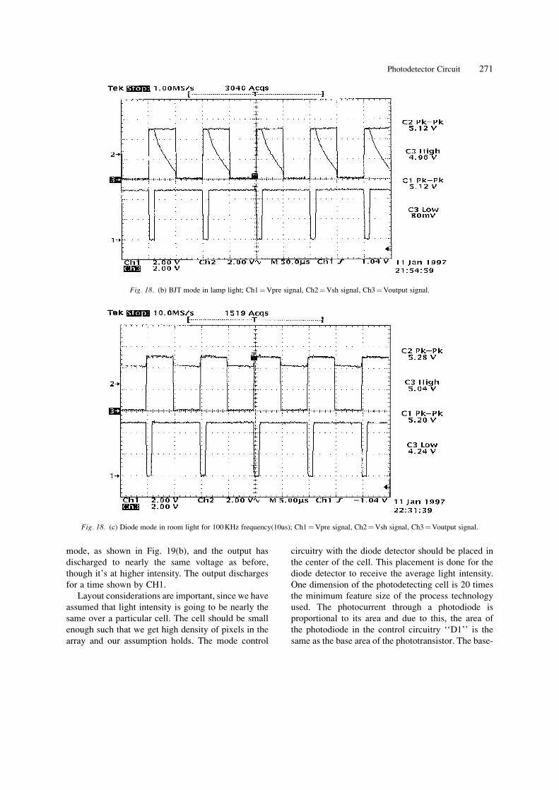
Fig. 18. Experimental results for multimode photodetector circuit. (a) Diode mode in lamp light; Ch1�Vpre signal, Ch2�Vsh signal,
Ch3�Voutput signal.
270 A. Khan, A. Deval and L. A. Akers
mode, as shown in Fig. 19(b), and the output has
discharged to nearly the same voltage as before,
though it's at higher intensity. The output discharges
for a time shown by CH1.
Layout considerations are important, since we have
assumed that light intensity is going to be nearly the
same over a particular cell. The cell should be small
enough such that we get high density of pixels in the
array and our assumption holds. The mode control
circuitry with the diode detector should be placed in
the center of the cell. This placement is done for the
diode detector to receive the average light intensity.
One dimension of the photodetecting cell is 20 times
the minimum feature size of the process technology
used. The photocurrent through a photodiode is
proportional to its area and due to this, the area of
the photodiode in the control circuitry ``D1'' is the
same as the base area of the phototransistor. The base-
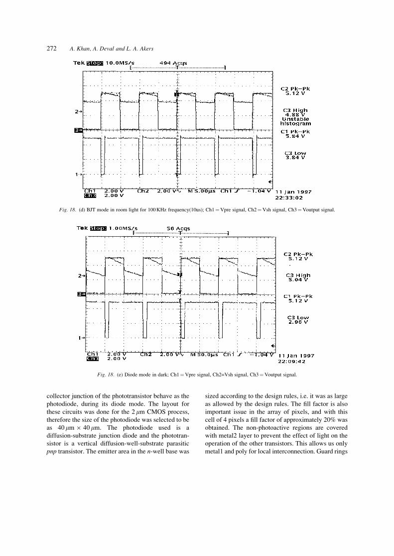
Fig. 18. (b) BJT mode in lamp light; Ch1�Vpre signal, Ch2�Vsh signal, Ch3�Voutput signal.
Fig. 18. (c) Diode mode in room light for 100 KHz frequency(10us); Ch1�Vpre signal, Ch2�Vsh signal, Ch3�Voutput signal.
Photodetector Circuit 271
collector junction of the phototransistor behave as the
photodiode, during its diode mode. The layout for
these circuits was done for the 2 mm CMOS process,
therefore the size of the photodiode was selected to be
as 40 mm6 40 mm. The photodiode used is a
diffusion-substrate junction diode and the phototran-
sistor is a vertical diffusion-well-substrate parasitic
pnp transistor. The emitter area in the n-well base was
sized according to the design rules, i.e. it was as large
as allowed by the design rules. The ®ll factor is also
important issue in the array of pixels, and with this
cell of 4 pixels a ®ll factor of approximately 20% was
obtained. The non-photoactive regions are covered
with metal2 layer to prevent the effect of light on the
operation of the other transistors. This allows us only
metal1 and poly for local interconnection. Guard rings
Fig. 18. (d) BJT mode in room light for 100 KHz frequency(10us); Ch1�Vpre signal, Ch2�Vsh signal, Ch3�Voutput signal.
Fig. 18. (e) Diode mode in dark; Ch1�Vpre signal, Ch2=Vsh signal, Ch3�Voutput signal.
272 A. Khan, A. Deval and L. A. Akers
have also been put for anti-blooming protection.
These guard rings also reduces the effect of cross
talk [7].
It is important to discuss the advantages and
disadvantages of the locally adaptive multimode
photodetector circuit. As stated earlier the main
advantage of this circuit is its excellent sensitivity
over large dynamic range. The dynamic range of the
circuit is also comparable to the other circuits. The
dynamic range of this circuit is calculated as
approximately 95 dB. The other advantage of this
circuit is the scheme is cellular based and it
implements local adaptation instead of global adapta-
tion. The drawback of this circuit is its large dark
Fig. 18. ( f ) BJT mode in dark; Ch�Vpre signal, Ch2�Vsh signal, Ch3�Voutput signal.
Fig. 19. Experimental results for locally adaptive multimode photodetector circuit. (a) BJT mode in room light for Vref� 3 V; Ch1�Vsh
signal, Ch3�Voutput signal, Ch4�Vmode signal.
Photodetector Circuit 273
current due to the transistor action which can be
observed from the experimental results. Due to the
limitation of the testing equipment, the leakage of
current in a oscilloscope is comparable to the dark
current and we do not observe signi®cant change in
voltage for different modes in the dark. This has the
effect of reducing the dynamic range, but the range
achieved with this circuit is comparable to existing
circuits. Another drawback is its less ®ll factor, but
with clever layout techniques this could be improved.
The other problems of this circuit are similar to the
ones suffered by other circuits such as ®xed pattern
noise, scaling problem, blooming, lag etc. General
techniques such as correlated double sampling,
uniform doping, etc. can be used to reduce these
effects for this circuit also.
5. Summary
We have given a description of the design and
measurement of the locally adaptive multimode
photodetector circuit. Simulation supported with the
hardware results were presented. The advantages and
drawbacks of this circuit were also brought out. This
circuit can be used in applications where light
intensity is varying locally over large orders of
magnitude and sensitivity is a crucial factor.
References
1. E. R. Fossum, ``Active Pixel Sensors challenge CCDs.'' LaserFocus World, pp. 83±87, 1993.
2. V. Ward, M. Syrzycki, and G. Chapman, ``CMOS
Photodetector with Built in Light Mechanism.''
Microelectronics Journal 24, pp. 547±553, 1993.
3. T. Delbruck and C. Mead, ``Phototransduction by Continuous
Time, Adaptive, Logarithmic Photoreceptor Circuits.'' Tech.Rep. California Institute of Technology, Pasadena California
91125, 1994. URL: http://www.pcmp.caltech.edu/anaprose/
tobi/recep.
4. Vision Chips Web site, URL: http://www.eleceng.adelaide.e-
du.au/Groups/GAAS/ Bugeye/visionchips/
5. M. A. Mahowald, ``Silicon Retina with Adaptive
Photodetector.'' Proc. SPIE, Visual Information Processingfrom Neurons to Chips 1473, pp. 52±58, 1991.
6. R. Nixon, S. E. Kemeny, C. O. Staller, and E. R. Fossum,
``2566 256 CMOS Active Pixel Sensor Camera on a Chip.''
ISSCC `96, pp. 178±179, 1996.
7. O. Y. Pecht and R. Ginosar, ``A Random Access Photodiode
Array for Intelligent Image Capture,'' IEEE transactions onelectron devices 38(8), pp. 1772±1779, 1991.
8. K. A. Boahen and A. G. Andreou, ``AContrast Sensitive Silicon
Retina with Reciprocal Synapses,'' Advances in NeuralInformation Processing 4, pp. 762±772, 1992.
9. A. Moini and A. Bouzerdoum, ``A Current Mode
Implementation of shunting Inhibition,'' ICNN '97 (accepted).
10. K. Boahen, ``Retinamorphic Vision Systems I: Pixel Design.''
Physics of computation Laboratory, California Institute of
Technology, MS 136±93, Pasadena, CA 91125.
11. S. Espejo, A. R. Vazquez, R. D. Castro, J. L. Huertas, and E. S.
Sinencio, ``Smart-Pixel Cellular Neural Networks in Analog
Current-Mode CMOS Technology.'' IEEE journal of solid statecircuits 29(8), pp. 895±904, 1994.
Fig. 19. (b) Diode mode in lamp light for Vref� 3 V; Ch1�Vsh signal, Ch3�Voutput signal, Ch4�Vmode signal.
274 A. Khan, A. Deval and L. A. Akers
12. B. Fowler, ``CMOS Area Image Sensors with Pixel level A/D
conversion.'' Ph.D. Dissertation, 1995. URL: http://www.isl.-
stanford.edu/people/fowler/thesis2.ps.gz
13. N. H. E. Weste and K. Eshraghian, ``Principles of CMOS VLSI
Design: A Systems Perspective.'' 2nd ed., Addison Wesley,
Reading, Massachusetts, 1993.
14. H. Wong, ``Technology and Device Scaling Considerations for
CMOS Imagers.'' Solid State Circuits Technology Workshop
on CMOS Imaging Technology, San Francisco, CA, 1996.
Dr. Lex A. Akers is the Janey and Dolph
Briscoe Distinguished Professor of Engineering and
Director of the Division of Engineering at the
University of Texas at San Antonio.
He received his B.S. in Electrical Engineering in
1971, his Master of Science in Electrical Engineering
in 1973, and his Doctor of Philosophy in 1975, all at
Texas Tech University
He was previously a Professor of Electrical
Engineering and Director of the Center for Solid
State Electronics Research at Arizona State
University. He has also worked at Southwest
Research Institute, Motorola, Intel, Rockwell, and
the Jet Propulsion Lab.
He is a fellow of the IEEE and is internationally
known for his research in Analog Neural Circuits and
Networks, Architectures with Nanostructured Devices
and Circuits, and Modeling Submicron CMOS
Devices
He is the author or co-author of more than 90
scienti®c articles, and 12 books or book chapters.
Amjad M. Khan received the B.E. degree in
Electronics and Communication Engineering from MJ
College of Engineering and Technology, Osmania
University, Hyderabad, India in 1995. He received the
M.S. degree in Electrical Engineering from Arizona
State University, Tempe, Arizona, in 1997.
Presently, he is a Component Design Engineer in
Microprocessor Product Group of Intel Corporation,
Folsom, California. His current research interests
include High Speed I/O circuits, CMOS active pixel
sensors and Analog VLSI Design.
Anant Deval was born on October 4, 1973 in
Manchester U.K.. He received his Bachelors Degree
in Electronics and Communication Engineering from
Delhi Institute of Technology, Delhi, India in 1995
and his Masters in Electrical Engineering from
Arizona State Univarsity, Tempe, Arizona, USA in
1997. He is currently working with Intel Corporation
as a Design Engineer. His interests include Adaptive
systems, computer architecture and low power circuit
design.
Photodetector Circuit 275
Related Documents