A HIGH-SPEED, HIGH-RESOLUTION SIGMA-DELTA MODULATOR ANALOG-TO-DIGITAL CONVERTER by LIEYIFANG, B.S.,M.S. A DISSERTATION IN ELECTRICAL ENGINEERING Submitted to the Graduate Faculty of Texas Tech University in Partial Fulfillment of the Requirements for the Degree of DOCTOR OF PHILOSOPHY Approved Chair]^erí/on of the Committee Accepted -4AM—^ 1 1 . m-»^ Dean of the Graduate School May, 2004

Welcome message from author
This document is posted to help you gain knowledge. Please leave a comment to let me know what you think about it! Share it to your friends and learn new things together.
Transcript

A HIGH-SPEED, HIGH-RESOLUTION SIGMA-DELTA
MODULATOR ANALOG-TO-DIGITAL CONVERTER
by
LIEYIFANG, B.S.,M.S.
A DISSERTATION
IN
ELECTRICAL ENGINEERING
Submitted to the Graduate Faculty
of Texas Tech University in Partial Fulfillment of the Requirements for
the Degree of
DOCTOR OF PHILOSOPHY
Approved
Chair]^erí/on of the Committee
Accepted
-4AM—^ 1 1 . m-»^
Dean of the Graduate School
May, 2004


ACKNOWLEDGMENTS
First, I would like to express my gratefulness to Professor Kwong S. Chao, for his
continuous support, guidance, patience and friendship during the course of this work.
Without his encouragement, the success of this work would never have been possible. I
also would like to sincerely thank Professor Thomas Krile, Professor Sunanda Mitra, and
Professor Thomas F. Trost for their willingness to be my committee members, and their
time spent on advising of this work.
This work is supported in part by Texas Instruments Inc, Dallas. For this, I am
thankful to Mr. David Devincal, Dr. Eric Sonen, Dr. Frank Tasy, Mr. Hugh Mair, and Dr.
Hydar Bilhan. Technical discussions with Dr. Feng Chen and Dr. Ramesh
Chandrasekaran, on many respects such as design, layout, fabrication, and testing have
been extremely beneficial. Assistance from other staff members in Texas Instruments,
Inc. is also appreciated.
I owe special thanks to my peers, Martin Kinyua, Zhongqiang Zheng, Yeshoda
Devi Yedevelly, and Chun Hsien Su for many discussions and help.
I appreciate the support from the Department of Electrical and Computer
Engineering.
Thanks also go to my parents, brothers, and sister for their unfailing love.
Finally, but not least, I would like to dedicate this thesis to my wife, Lanyun Gao,
my daughter, Rebecca, and my son, David, for their unprecedented love and support
throughout my graduate studies. Without them, my study here would not be possible.

CONTENTS
ACKNOWLEDGMENTS i
ABSTRACT vi
LISTOFTABLES vii
LIST OF FIGURES viii
CHAPTER
1. INTRODUCTION 1
2. ANALOG-TO-DIGITAL CONVERTER 4
2.1. Overview 4
2.2. Typical specifications of analog-to-digital converters 6
2.3. Types of analog-to-digital converters 7
2.4. Limitations of conventional converters 9
3. BASICS OF OVERSAMPLING SIGMA-DELTA MODULATOR 11
3.1. Overview 11
3.2. Concepts used in the sigma-delta modulator 12
3.3. Simple sigma-delta modulator 16
3.4. High-order sigma-delta modulator 20
3.5. Advantages 25
3.6. Limitations and questions 25
4. MULTI-BIT SIGMA-DELTA MODULATOR BASED ADC 27
4.1. Overview 27
11

4.2. Multi-bit sigma-delta modulator without multi-bit DAC 30
4.3. Other multi-bit sigma-delta modulator systems 34
4.3.1. Multi-bit sigma-delta modulator ADC with multi-bit DAC error cancellation 34
4.3.2. Multi-bit sigma-delta modulator ADC with interstage feedback 39
4.3.3. Multi-bit sigma-delta modulator with high order noise shaped integrator leakage 44
5. ARCHITECTURE AND BEHAVIORAL SIMULATION 51
5.1. System architecture 53
5.2. Nonideahties 57
5.2.1. Integrator leakage error 57
5.2.2. Multi-bit quantizer and the nonideahties 58
5.3. System simulation 59
5.4. Circuit specifications 61
6. CMOS VLSIIMPLEMENTATION 63
6.1. Capacitors 63
6.2. Operational amplifier 65
6.2.1. Two-stage op-amp and design equations 67
6.2.1.1. Core circuit 67
6.2.1.2. Design equations 69
6.2.1.3. Design considerations 73
6.2.2. Common-mode feedback 76
6.2.3. Bias circuit design 78
111
6.2.4. Simulation results 79
6.2.5. Layout 81
6.3. Comparator 82
6.4. Switches 85
6.4.1. Signal dependent on-resistance 86
6.4.2. Charge injection 88
6.4.3. Simulation results 90
6.5. Second-order modulator 92
6.6. Pipeline ADC 96
6.7. First-order modulator 98
6.8.FIash ADC 100
6.9. Clock generator 102
6.9.1. Nonoverlapped two-phase clock generator 102
6.9.2. Clockjittereffect 102
6.10. System integration and layout issues 104
7. EXPERIMENTAL RESULTS 107
7.1.Testsetup 108
7.2. Dynamic linear range 109
7.3. Discussion 111
8. CONCLUSIONS 114
REFERENCES 115
IV

APPENDIX
A. SWITCHED CAPACITOR INTEGRATOR 120
B.NONIDEALITIESOFPIPELINEA/DCONVERTERS 127
C. SETTLING OF THE OPERATIONAL AMPLIFIER 134
D. NOISE CALCULATION IN 5C CIRCUITS 145

ABSTRACT
Sigma-delta modulators provide the means for achieving high-resolution analog-
to-digital conversion. The main hmitation faced in the high-resolution Sigma-Delta
approach is conversion speed. A multi-stage multi-bit sigma-delta modulator with
interstage gain scaling is proposed in this study, and it is designed and implemented in a
0.6 |am CMOS process. This topology employs a second-order single-bit modulator in the
main stage foUowed by an 8-bit quantizer in pipeline structure. The second stage of the
modulator consists of a first-order single-bit modulator followed by a 5-bit quantizer. A
gain stage is inserted between the two stages to scale the signal level to within the
reference level.
System and circuit level simulations have demonstrated that the proposed
modulator is capable of achieving high speed and high resolution in analog-to-digital
conversion. The detailed design considerations in circuit implementation of the proposed
modulator are also analyzed and discussed. The prototype is fabricated in a 0.6 im
CMOS process with 3.3V power supply. Experimental measurement of the prototype is
performed. Several factors limiting the performance are discussed.
VI

LIST OF TABLES
3.1. Reduction of the quantization noise power 16
3.2. The value at different nodes of the modulator in the first 10 steps 18
5.1. The high speed sigma-delta modulator converters 52
5.2. The relationships among analog coefficients and digital coefficients 57
5.3. The circuit specifications 62
6.1. Transistors size of the op-amp core 75
6.2. Summary of the op-amp 80
7.1. Summary of testing results 111
vii

LIST OF FIGURES
2.1. A typical analog-to-digital converter 4
2.2. An example of a uniform multilevel quantization characteristic that is represented by linear gain G and errorE 5
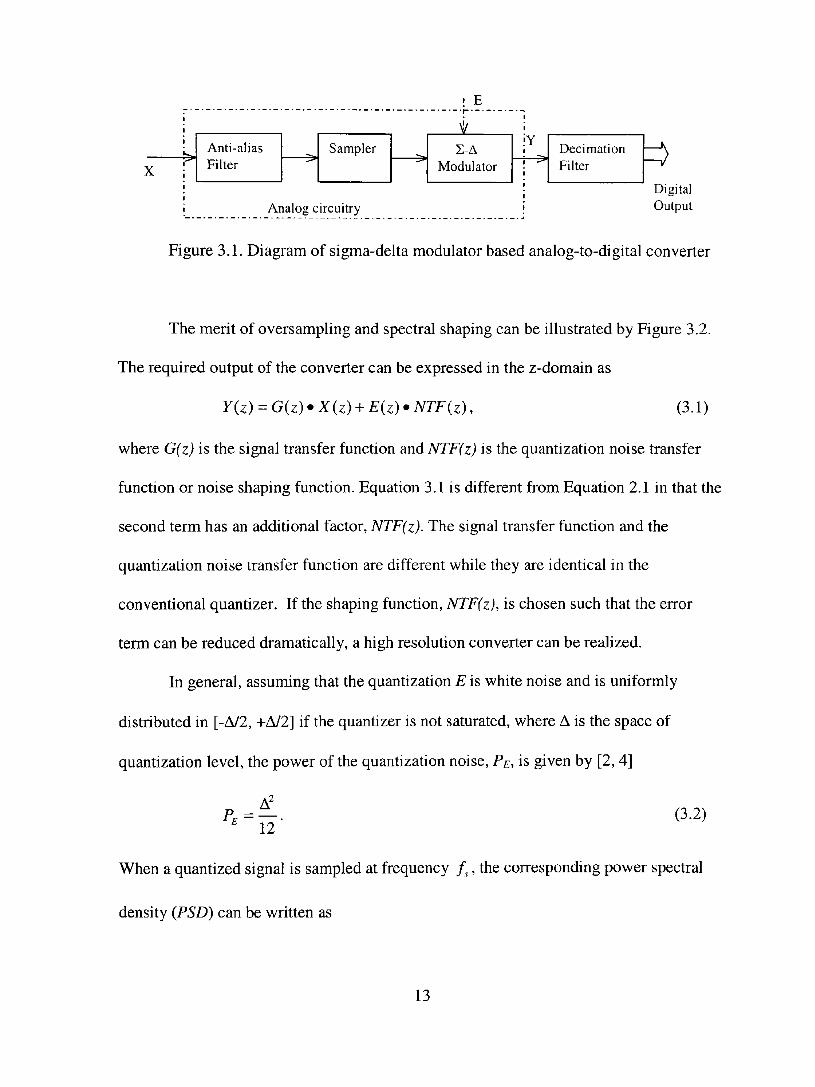
3.1. Diagram of sigma-delta modulator based analog-to-digital converter 13
3.2. Diagram of power spectral density of quantization noise of Nyquist converters, oversampling converters, and oversampling plus noise shaping converters 14
3.3. Noise shaping function (NSF) 16
3.4. A simple first order sigma-delta modulator 17
3.5. Integrator output u(kT) and the averaged output value of q(kT) as a
function of time 19
3.6. Pulse density modulation output to sinusoidal input in time domain 20
3.7. Dynamic range as a function of oversampling ratio r and order L of the single-bit modulator 21
3.8. Second-order double-integrator sigma-delta modulator proposed
byCandyin 1985 22
3.9. Multi-stage sigma-delta modulator leads to the high-order modulator 23
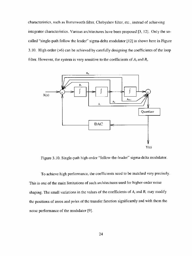
3.10. Single-path high-order "follow-the-leader" sigma-delta modulator 24
3.11. Trade off between the resolution and speed for various converters 26 4.1. A simple first-order sigma-delta modulator employing an intemal multi-bit
quantizer and a multi-bit DAC 28
4.2. The topology (a) and its equivalent scheme (b) of a multi-bit sigma-delta modulator proposed by LesUe and Singh in 1990 31
4.3. The system topology proposed by Kinyua and Chao (1997) andBrooks,Robertson, andKelIy(1997) 32
Vll l

4.4. The system employing interstage scaling concept proposed by Chandrasekaran and Chao (1997) 33
4.5. The proposed system. I](z) and ^(z) are integrators. Hi(z) and H2(z) aredigital filters 35
4.6. Baseband power spectral density of the output of the proposed structure (top figure), the regular MASH topology with ideal multi-bit DAC (middle figure) and with nonideal multi-bit DAC (bottom figure) in the feedback loop of the second stage 38
4.7. SNR for the proposed structure (upper curve) and that of the regular MASH topology with nonideal multi-bit DAC (lower curve) as a function of input signal level 38
4.8. The multi-bit sigma-delta modulator employing interstage feedback 39
4.9. Comparison of various modulators in terms of quantization noise level reduction 41
4.10. Baseband power spectral density for the proposed system (lower curve) and that of the system (upper curve) in [23] and [24], the spikes in the graph is that of the input signal 43
4.11. SNR for the proposed system (upper curve) and that of the system (lower curve)
in [23] and [24] as afunction of input signal level 43
4.12. A multi-bit system with gain and pole errors being spectrally shaped 45
4.13. The extension of the system in Figure 4.12 to high order noise shaping 47
4.14. The power spectral density (PSD) of the output of both systems with both gain error andpole error are assumedto be 0.01 48
4.15. The effect of gain and pole errors on signal-to-noise ratio for the proposed system and the system in [20] 49
5.1. The performance of published sigma-delta modulator analog-to-digital converters in terms of resolution and signal bandwidth 52
5.2. Block diagram of the system 54
IX

5.3. The topology of third-ordermulti-bit sigma-delta modulator 56
5.4. The integrator output probabiHty density for a -6dB input signal 60
5.5. Power spectral density (PSD) of the sigma-delta modulator shown
inFigure 5.3. PSD in the baseband is shown at the bottom 61
6.1. The schematic of a typical two-stage amplifier core 67
6.2. The high frequency differential half-equivalent circuit for two-stage
amphfier shown in Figure 6.1 68
6.3. The continuous time common-mode feedback network 76
6.4. The switched-capacitor common-mode feedback network 77
6.5. Bias circuit employing extemal current reference 78
6.6. AC sweep of Spice simulation 80
6.7. The block of paired transistors 81
6.8. The layout of the op-amp 82
6.9. The schematic of the comparator 84
6.10. Layout of the comparator 85
6.11. Diagram of the sampling capacitor and switches and the equivalent circuit 86
6.12. The diagram of the sampling switch and capacitor (a), the MOSFET implementation (b) 89
6.13. Thediagram showing the clock feedthrough and charge injections 89
6.14. The power spectral density of the input signal and the harmonic distortions 91
6.15. The schematic of second-order sigma-delta modulator 95
6.16. The schematic of one stageof the pipehned ADC 98
6.17. The schematic of the first-order sigma-delta modulator 100
6.18. Theschematicofaflash ADC 101
6.19. The schematic of the clock generator 103
6.20. The uniform density function of the clock jitter 103
7.1. Die photograph of the prototype 107
7.2. Testing setup 108
7.3. Power spectral density of input signal level at-3dB 110
7.4. Power spectral density of first stage output when inputs are
shorted to PCB board 112
A. 1. Half circuit of the switched-capacitor integrator 120
B.l. Diagram of generic B-bit-per stage pipeline ADC 127
B.2. Diagram of 1.5-bit-per stage switched-capacitor A/D converter 131
B.3. Residue plot of 1.5-bit-per stage algorithmic ADC for ideal case 133
C. 1. Equivalent configuration of amplification phase or integrating phase 134
C.2. The equivalent circuit of a two-stage op-amp 142
D.l. The configuration of the gain stage during the amplification phase or that of integrator during the integrating phase 146
XI

CHAPTER I
INTRODUCTION
Data converters which include analog-to-digital converters (ADCs) and digital-to-
analog converters (DACs) are the devices that provide the link between the analog world
of the transducer or actuator and the digital world of signal processing, computing, digital
data collection or digital data processing [1]. They convert the analog signals to digital
counterparts which are processed in the digital domain or convert the digital code to
analog signals. High performance data converters are always in demand in view of the
rapid development of computing and digital signal processing. For example, the
consumer products such as compact disc players, camera recorders (CAMCORD),
telephones, modems, high-definition television (HDTV), asymmetrical digital subscriber
line (ADSL), etc, require a high resolution and/or high speed data converter to interface
to the analog world [2, 3, 4, 5].
The performance of digital signal processing and communication systems is
generally limited by the performance of the data converters. Achieving high resolution in
conventional data converters other than the sigma-delta modulator based approaches
requires high precision analog components that are very difficulty and costly in a Very
Large Scale Integrated (VLSI) process. The problem becomes more and more severe as
feature sizes of VLSI processes continue to shrink. On the contrary, the high precision
component matching and trimming are not needed in sigma-delta modulator based data
conversion technology. It is a cost effective altemative for high resolution (greater than

16 bits) converters which can be ultimately integrated on digital signal processor
integrated circuits (ICs).
Sigma-delta modulator based data converters use a coarse quantizer, for example
single bit, to achieve high resolution by employing two basic principles: oversampHng
and spectral shaping. The in-band quantization noise is reduced by the spectral shaping
function; the out-of-band noise is removed by the digital decimation filter. The overall
quantization noise is dramatically reduced. The resolution can be increased to as many as
20 or more bits by simply increasing the oversampling ratio and the order of the shaping
function [2, 3,4]. There is good linearity and accuracy. Since the signal bandwidth to be
converted is limited by the nature of the oversampling, it has seen applications mostly in
digital audio (low-frequency range). However, there is ever increasing need to apply
high-speed data converters with high resolution in the area of modem communication
systems such as ISDN, ADSL. This leads to the trend of extending the application of
sigma-delta modulator based data converters to higher signal frequencies. The problem
of how to achieve wide signal bandwidth, hence high speed, while retaining the high
resolution becomes a very important and interesting issue in the design of sigma-delta
modulator converters.
In this thesis, several system topologies that lead to high resolution and high
speed sigma-delta modulators are proposed and studied. One of these topologies based
on interstage scaling has been implemented and fabricated in a 0.6um, double-poly and
triple-metal 3.3voIts CMOS process.

In the context of this thesis, an overview of the conventional analog-to-digital
converters is described in Chapter 2. Different types of converters and their hmitations
are also briefly discussed. In Chapter 3, the basics of the sigma-delta modulator are
reviewed and several architectures are discussed along with their advantages and
limitations. In Chapter 4, the multi-bit sigma-delta modulator is reviewed and the existing
topologies are introduced. Some useful topologies leading to high-speed and high-
resolution modulators are proposed and reviewed. In Chapter 5, the high-speed, high-
resolution, sigma-delta modulator architecture and behavioral simulation are given. The
detailed VLSI implementation in 0.6um CMOS process is presented in Chapter 6.
An experimental prototype sigma-delta modulator has been fabricated, and its
results are presented in Chapter 7 along with discussions on key performance issues.
Finally, the conclusions are given in Chapter 8.
CHAPTER 2
ANALOG-TO-DIGITAL CONVERTER
2.1 Overview
As mentioned in Chapter 1, the analog-to-digital converter is the type of device
that converts the signals in the analog domain to its digital counterpart that can be
processed by a computer or digital signal processor in the digital domain.
An analog-to-digital converter performs two basic operations: sampling in time
and quantizing in amphtude [1, 2]. A typical analog-to-digital converter is shown in
Figure 2.1.
Analog Input
"^ ^
Anti-alias Filter
Ar
' ^ i
-^
lalog c
Sampler
ircuitry
X
->
! E
\/
Quantizer Y
^ Encoder
^
Digital Output
Figure 2.1. A typical analog-to-digital converter
The low-pass filter is an anti-alias filter that removes the components outside the
signal bandwidth to be converted. It eliminates aliasing when the Nyquist sampler is
applied. The analog signal is sampled in time and quantized in amplitude. The
quantization levels are encoded, resulting in digital code outputs. The digital code can
enter a computers or digital signal processors for signal conditioning. The sampling in
time results in discrete signals, and the quantization in amphtude causes errors to the
signal quantized. Figure 2.2 shows a uniform quantization that rounds off a continuous
signal X to integers in the range of ±5. In this example, the level space A is 2.
- > X
Y=GX+E
Figure 2.2. An example of a uniform multilevel quantization characteristic that is represented by linear gain G and error E.
The relationship between the quantized output Y and analog input X can be
described by the following equation:
Y = G^X-\-E, (2.1)
where E is quantization error and G, the overall gain of the converter, is arbitrary. It is
seen that the output signal of the quantizer is not exactly equal to the input signal. It is
contaminated by the error term E.

2.2 Typical specifications of analog-to-digital converters
Many types of specifications for analog-to-digital converters are quoted by
hardware manufacturers. Here only four are used: resolution, linearity, dynamic range,
and throughput; and they are explained in this section.
a. Resolution: The resolution of an analog-to-digital converter is the number of steps
the input range is divided into. The resolution is usually expressed in bits {n) and the
number of steps is expressed as 2 to the power n. With 12-bit resolution, for instance,
the range is divided into 2^ , or 4096, steps. In this case a -1 to 1 V range will be
resolved to 0.5mV, and a -lOOmV to lOOmV range will be resolved to O.OSmV.
Although the resolution can be increased if the input range is narrowed, there is no
point in trying to resolve signals below the noise level of the system; all one can get is
unstable readings.
b. Linearity: Ideally, an analog-to-digital converter with n-bit resolution will convert
the input range into 2n-l equal steps (4095 steps in the case of a 12-bit converter). In
practice, the steps are not exactly equal due to the nonlinearity of the circuits. This
leads to the nonlinearity in a plot of the analog-to-digital output against the input
amplitude.
c. Dynamic range: Dynamic range is the ratio of maximum allowable input level and
the minimum input level that can be converted in a monotonic and linear manner. It is
limited by the non-linearity of the conversion circuit. Ideally, the signal-to-noise plus
distortion ratio (SNDR) of the converter will be a straight line with different input

levels. However, there are many factors that limit the allowable input level in
practice.
d. Throughput: The throughput is the maximum rate at which the analog-to-digital
converter can output data values. In general, it will be the inverse of the samphng
periods of the analog-to-digital converter. Thus a converter that takes 0.1|Lis to acquire
and convert will be able to generate lOM samples per second. The throughput is
lOM/sec. in this case. Throughput can be increased by the use of pipeline stmctures,
such that a second conversion can start while the first is still in progress. Throughput
may be slowed down, however, by some factors that prevent data transfer at the full
rate.
2.3 Tvpes of analog-to-digital converters
Numerous types of analog-to-digital converters have been designed and
manufactured in VLSI processes. Those types typically used, such as flash converter,
pipelined converter, successive approximation converter, folding converter, and sigma-
delta modulator converters, are described briefly in this section.
a. Flash Converter. A flash converter is the fastest type of converter. It works by
comparing the input signal to a reference voltage, but a flash converter has as many
comparators as there are steps in the comparison. For an n-bit converter, the number
of comparators used will be ^''-l, which makes the high resolution (n>10) impractical.
With n=10, for instance, 1023 comparators are required and operated in parallel. This
makes the input capacitance too large, thus slowing down the operation speed.
Moreover, the reference step is Vref/1023, which is diffícult to achieve in the
modem VLSI process. In addition, a considerable amount of digital logic is required
to encode the comparator's outputs. The resolution of a flash converter is usually 8
bits or less.
b. Pipeline Converîer. A pipeline converter uses the concept of pipelining often used in
digital circuits. It can achieve higher speed where several operations are performed
serially. Generally, a pipehne converter consists of many conversion stages. Each
stage is a coarse quantizer that carries out an operation on a sample and passes the
residue to the following conversion stage. Once the result is passed on, each stage is
free to process the next sample coming down the pipe. Thus, at any given time, all the
stages are processing different samples concurrently. The throughput depends only on
the speed of each stage and the acquisition time of the next stage. A simple pipeline
converter is a one-bit-per-stage stmcture in which each stage resolves only one bit.
With n-bit resolution, n conversion stages are required, and n-1 operational amplifiers
are required to sample and hold the residuals of previous stages. The pipeline
converter with multi-bit quantizer in each stage is also designed such that a small
number of operational amplifiers is required; thus the power consumption is reduced.
In practice, pipehne converters can achieve up to 14 bits.
c. Successive approximation converter. A successive approximation converter (SAR)
works by first comparing the input signal with a voltage which is half of the input
range. If the input is larger than this level, it compares it with three quarters of the
range, and so on. If the input is below this level, it compares with a quarter of the full

input range, and so on. With n-bit resolution, n such steps are required; for instance,
twelve such steps gives 12-bit resolution. As these comparisons are taking place, the
signal is frozen in a sample and hold circuit. Practically, up to 14 bits of resolution is
possible. Usually sophisticated digital logic is needed.
d. Folding converter. A folding converter evolved from flash and two-step topologies
[6]. Flash converters are operated in one step without the need for post-processing,
but they suffer from the large input capacitance, large power dissipation, severe
offset, and severe timing problems as speed and resolution increase. Two-step
architecture, on the other hand, has much less hardware but requires a front-end
sample-and-hold circuit as well as analog post-processing. Folding architectures
perform analog preprocessing to reduce the hardware while maintaining the one-step
nature of flash architecture. The basic principle in folding is to generate a residue
voltage through analog preprocessing and subsequently quantize the residue to obtain
the least significant bits. The most significant bits can be resolved using a coarse flash
stage that operates in parallel with the folding circuit and hence samples the signal at
approximately the same time that the residue is sampled. It differs from the two-step
flash converter in that the residue is generated using simple wideband stages instead
of using a multi-bit DAC and an analog subtractor.
e. Sigma-delta modulator converter: A sigma-delta modulator converter is a new type of
converter. It emerged in the mid-1980s. It achieves extremely high resolution with
lower precision analog components. For example, it achieves more than 16-bit
resolution by employing only a one-bit quantizer. In general, very complex digital

circuitry is required for the decimation filter. Usually, no sample/hold and anti-alias
filter is necessary at its input. Up to 20-bit resolution can be achieved.
2.4 Limitations of conventional converters
Achieving high resolution requires high precision analog components in the
conventional converters. Consider a flash converter, for instance, with 12-bit resolution:
4095 comparators are required. The reference step is V^^j- /4095. If V^^j- = IV is assumed,
the reference step is only 0.24mV. Such fine steps are well below the offsets of the
comparators and the mismatch of the components used to obtain the reference voltages.
The offsets of the operational amplifier and comparators used in a pipeline converter also
make it difficult for the converter to achieve high resolution (>12-bit) in practice. In
addition, with VLSI offering high speed and high density, the accuracy of the analog
component is reduced. The signal range, thus the dynamic range, is also reduced due to
the scale down of the power supply. Moreover, the environment of the circuits becomes
noisy when more and more circuits are integrated into a single chip. The noisy
environments make the matching even worse. Therefore, it is impractical to achieve high
resolution in conventional converters.
10

CHAPTER 3
BASICS OF OVERSAMPLING SIGMA-DELTA MODULATOR
3.1 Overview
The use of oversampling and single-bit code words can be dated back to 1946
when delta modulation was fírst proposed. Many modifícations and variants of the delta
modulator have been suggested since then [2]. In a delta modulator, a coarse quantizer is
used and its output is integrated and subtracted from the input signal; the signal
difference between the input signal and the output of the integrator is the input of the
quantizer. The overall output of the modulator is the differentiation of the input signal
plus the quantization noise. The signal can be recovered by applying an integrator used at
the receiver; as a result, the quantization noise is shaped.
The techniques to spectrally shape noise, namely noise shaping, had been
proposed by Culter in 1954 [7]. His idea was to take a measure of the quantization error
in one sample and subtract it from the next input sample. Sigma-delta modulation
employing noise shaping was proposed by Inose and Yasuda in 1962 [8]. It is performed
by a delta modulator with the input signal integrated before entering into it. It eliminates
the need of using an integrator for the delta modulator to recover the input signal at the
receiver. However, this technique had not been used in practice until the mid-1980s,
because the use of a sigma-delta modulator required a digital decimation filter
suppressing the high frequency noise which was not realistic to build. In the mid-1980s,
the VLSI technology, especially the CMOS technology, had been advanced to
11

incorporate the digital signal processing circuits into a single chip [2]. Since then, sigma-
delta modulator based data converters have become a research area of interest.
There are two main application fields for oversampling sigma-delta modulator
converters. The first is the baseband converters, where the bandwidth is from dc to/s.
The other one is the bandpass sigma-delta modulators, where the modulator is designed
to perform noise shaping with the zeros of the noise transfer function placed at —/^
instead of dc. The bandwidth it converts is —/^ — / ^ to —/^ + —/^ [9]. In the context
of this thesis, only the former is discussed.
3.2 Concepts used in the sigma-delta modulator
Sigma-delta modulator based analog to digital converters employ two basic
concepts, oversampling and spectral noise shaping. The diagram of a sigma-delta
modulator based analog to digital converter is shown in Figure 3.1. Compared to the
conventional analog-to-digital converter, the quantizer in the diagram of Figure 2.1 is
replaced by the sigma-delta modulator in Figure 3.1, and the encoder there is replaced by
a digital decimation filter.
12
X s ^
Anti-alias Filter
• — f c
-.-* Sampler
Analog circuitry
í>
! E
ÍJ Z-A
Modulator
Y • j >
Decimation Filter ^
Digital Output
Figure 3.1. Diagram of sigma-delta modulator based analog-to-digital converter
The merit of oversampling and spectral shaping can be illustrated by Figure 3.2.
The required output of the converter can be expressed in the z-domain as
Y{z) = Giz) •X(z) + E{z) • NTF{z), (3.1)
where G(z) is the signal transfer function and NTF(z) is the quantization noise transfer
function or noise shaping function. Equation 3.1 is different from Equation 2.1 in that the
second term has an additional factor, NTF(z)- The signal transfer function and the
quantization noise transfer function are different while they are identical in the
conventional quantizer. If the shaping function, NTF(z), is chosen such that the error
term can be reduced dramatically, a high resolution converter can be realized.
In general, assuming that the quantization E is white noise and is uniformly
distributed in [-A/2, +A/2] if the quantizer is not saturated, where A is the space of
quantization level, the power of the quantization noise, PE, is given by [2, 4]
12 (3.2)
When a quantized signal is sampled at frequency / , the corresponding power spectral
density {PSD) can be written as
13

PSD,^ 12/.
(3.3)
where /^ is the sampling frequency. If the principle of oversampling is applied such that
the signal bandwidth converted /g = / .
2^0SR , where OSR is the oversampling ratio, then
the power of the quanzation error in the signal band becomes
E{0) 12 •OSR
(3.4)
Power Spectral Densitv A
/Quantization error of Nyquest converter
Quantization error of oveirsampling -i-noise shapi/ig
NTF(f)
Quantization error of oversampling converter
Figure 3.2. Diagram of power spectral density of quantization noise of Nyquist converters, oversampling converters, and oversampling plus noise shaping converters.
14
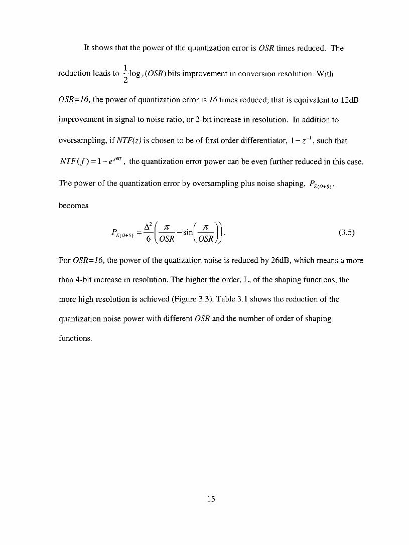
It shows that the power of the quantization error is OSR times reduced. The
reduction leads to — Iog2(05/?)bits improvement in conversion resolution. With
0SR=16, the power of quantization error is 16 times reduced; that is equivalent to 12dB
improvement in signal to noise ratio, or 2-bit increase in resolution. In addition to
oversampling, if NTF(z) is chosen to be of first order differentiator, l-z'\ such that
NTF{f) = l~e^^, the quantization error power can be even further reduced in this case.
The power of the quantization error by oversampling plus noise shaping, PE^O+S) '
becomes
p _ o
[^í ^ í ^ \^ n sin OSR
n (3.5) \OSRjj
For 0SR=16, the power of the quatization noise is reduced by 26dB, which means a more
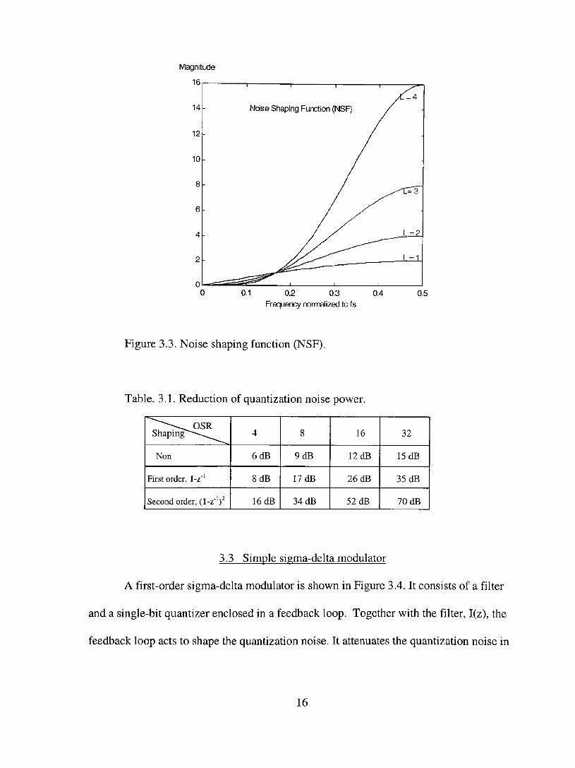
than 4-bit increase in resolution. The higher the order, L, of the shaping functions, the
more high resolution is achieved (Figure 3.3). Table 3.1 shows the reduction of the
quantization noise power with different OSR and the number of order of shaping
functions.
15
0.1 0.2 0.3 0.4 Frequency normalized to fs
0.5
Figure 3.3. Noise shaping function (NSF).
Table. 3.1. Reduction of quantization noise power.
Shaping^ -- ..... ^ ^
Non
Firstorder, l-z'
Second order, (l-z'^)^
4
6dB
8dB
16 dB
8
9dB
17 dB
34 dB
16
12 dB
26 dB
52 dB
32
15 dB
35 dB
70 dB
3.3 Simple sigma-delta modulator
A first-order sigma-delta modulator is shown in Figure 3.4. It consists of a filter
and a single-bit quantizer enclosed in a feedback loop. Together with the filter, I(z), the
feedback loop acts to shape the quantization noise. It attenuates the quantization noise in
16
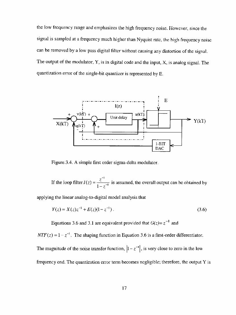
the low frequency range and emphasizes the high frequency noise. However, since the
signal is sampled at a frequency much higher than Nyquist rate, the high frequency noise
can be removed by a low pass digital fílter without causing any distortion of the signal.
The output of the modulator, Y, is in digital code and the input, X, is analog signal. The
quantizafíon error of the single-bit quantizer is represented by E.
+ _ v ( k î r ) -f-o ^ T O Aq(kT)
Y(kT)
Figure.3.4. A simple first order sigma-delta modulator.
If the loop filter/(z) = — is assumed, the overall output can be obtained by l-z
applying the linear analog-to-digital model analysis that
Y{z) = X{z)z-'+E{z){l-z-'). (3.6)
-1 Equations 3.6 and 3.1 are equivalent provided that G(z)~ z and
NTF{z) -l-z'^• The shaping function in Equation 3.6 is afirst-order differentiator.
The magnitude of the noise transfer function, l-z , is very close to zero in the low
frequency end. The quantization error term becomes negligible; therefore, the output Y is
17

a replica of the input signal X. So, ideally, the quanfízation error is suppressed but the
signal X is unaffected by the modulator. Note that any errors injected into the node after
the integrator will be noise shaped. Thus, unlike the conventional converters, the dc-
offset of of the comparators will not affect the performance of the sigma-delta modulator
converters.
The principles of how the sigma-delta modulator analog-to-digital converter
works can be illustrated by Table 3.2 and Figure 3.5.
Table 3.2. The value at different nodes of the modulator in first 10 steps.
k
0 1 2 3 4 5 6 7 8 9
x(kT)
0.1 0.1 0.1 0.1 0.1 0.1 0.1 0.1 0.1 0.1
v(kT)
-0.4 0.6 -0.4 0.6 -0.4 -0.4 0.6 -0.4 0.6 -0.4
u(kT)
0.1 -0.3 0.3 -0.1 0.5 0.1 -0.3 0.3 -0.1 0.5
q(kT)
0.5 -0.5 0.5 -0.5 0.5 0.5 -0.5 0.5 -0.5 0.5
e(kT)
0.4 -0.2 0.2 -0.4 0.0 0.4 -0.2 0.2 -0.4 0.0
y(kT)
1 0 1 0 1 1 0 1 0 1
Q(kT)
0.500 0.000 0.167 0.000 0.100 0.167 0.071 0.125 0.056 0.100
18

o o
D) 0
6 8 10 12 14 16 18 20 discrete time, k
>l)b
<*— o 3
5 • o 0) n) m 9 cO
0.2 1
0.1
0
-0.1 •
-0.2 •
40 60 80 discrete time, k
100 120
Figure 3.5. Integrator output u(kT) and averaged output value of q(kT) as a function of time.
Table 3.2 shows the value of different nodes in modulator for the first 10 steps.
Q(kT) is the averaged output value ofq(kT) over fíme. The averaged value, Q(kT), as a
function of the time k is shown in Figure 3.5. The output of the integrator, u(kT), is a
sawtooth waveform. It is predicted that Q(kT) becomes more and more close to the input
value x(kT)=0.1 when k increases. The principle can also be illustrated using a sinusoidal
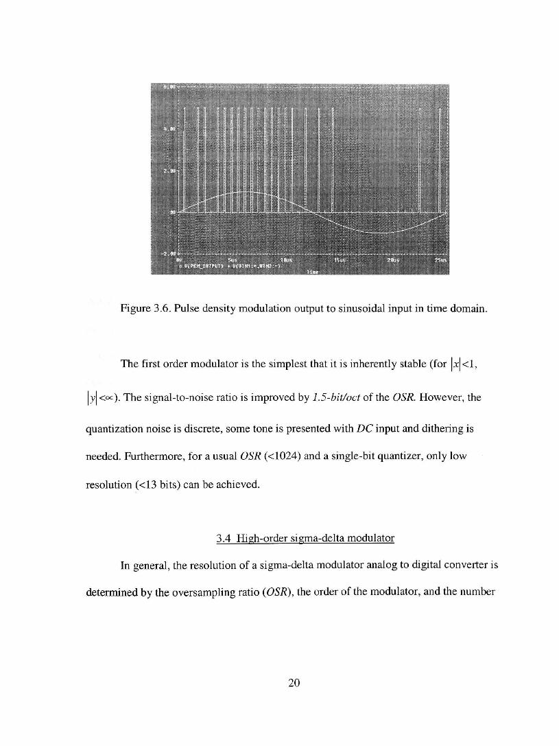
signal as input. Pulse density modulation output is obtained when a sinusoidal input is
applied (Figure 3.6); that is, the density of the output pulse is proportional to the
amphtude of the input signal. Obviously, the output and input of the modulator lack a
direct mapping relationship.
19
iiÊmfJ i W^
Figure 3.6. Pulse density modulation output to sinusoidal input in time domain,
The first order modulator is the simplest that it is inherently stable (for U <1,
\y\ <oc). The signal-to-noise ratio is improved by l.S-bit/oct of the OSR. However, the
quantization noise is discrete, some tone is presented with DC input and dithering is
needed. Furthermore, for a usual OSR (<1024) and a single-bit quantizer, only low
resolution (<13 bits) can be achieved.
3.4 High-order sigma-delta modulator
In general, the resolution of a sigma-delta modulator analog to digital converter is
determined by the oversampling ratio {OSR), the order of the modulator, and the number
20
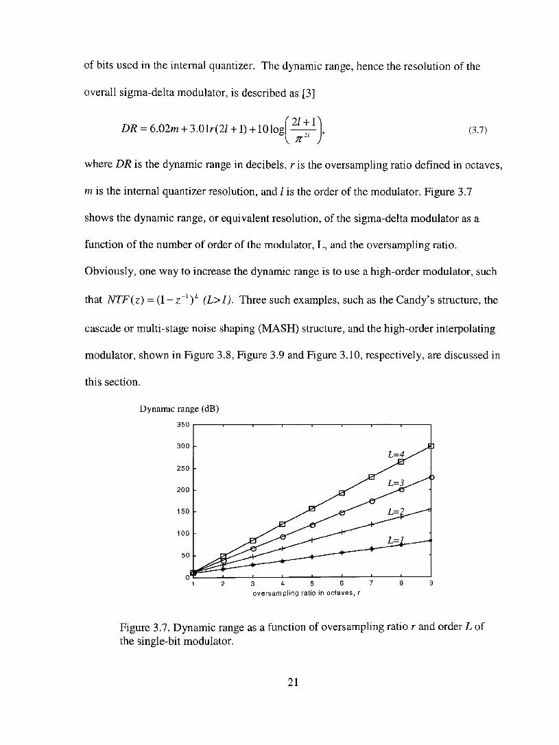
of bits used in the intemal quantizer. The dynamic range, hence the resolution of the
overall sigma-delta modulator, is described as [3]
Z)7? = 6.02m + 3.01r(2Z + l) + 10Iog 2/ + n
(3.7) \ n j
where DR is the dynamic range in decibels, r is the oversamphng ratio defined in octaves,
m is the intemal quanfízer resolution, and / is the order of the modulator. Figure 3.7
shows the dynamic range, or equivalent resolution, of the sigma-delta modulator as a
function of the number of order of the modulator, L, and the oversampling ratio.
Obviously, one way to increase the dynamic range is to use a high-order modulator, such
that NTF{z) = ( 1 - z~^)^ (L>1). Three such examples, such as the Candy's structure, the
cascade or multi-stage noise shaping (MASH) structure, and the high-order interpolating
modulator, shown in Figure 3.8, Figure 3.9 and Figure 3.10, respectively, are discussed in
this section.
Dynamic range (dB)
350
300
250
200
150
100
3 4 5 6 7 oversampling ratio in octaves, r
Figure 3.7. Dynamic range as a function of oversampling ratio r and order L of the single-bit modulator.
21
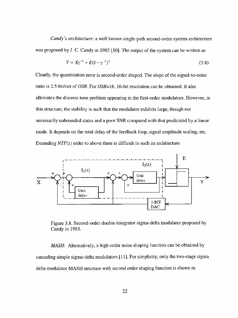
Candy's architecture: a well known single-path second-order system architecture
was proposed by J. C. Candy in 1985 [10]. The output of the system can be written as
Y = Xz-'+E{l-z-'y^ (3.8)
Clearly, the quantization error is second-order shaped. The slope of the signal-to-noise
ratio is 2.5-bit/oct of OSR. For 05i?=16, 16-bit resolution can be obtained. It also
alleviates the discrete tone problem appearing in the first-order modulators. However, in
this stmcture, the stability is such that the modulator exhibits large, though not
necessarily unbounded states and a poor SNR compared with that predicated by a linear
mode. It depends on the total delay of the feedback loop, signal amplitude scaling, etc.
Extending NTF(z) order to above three is difficult in such an architecture.
X <
i ' Líz^
f ^ 1
+
J ^ +
Unit delav
-^\ t\ >
+
i2(z) ;
Unit delav
f
1-BIT DA C
E
M
»
^ ^
Y
Figure 3.8. Second-order double-integrator sigma-delta modulator proposed by Candyinl985.
MASH: Altematively, a high-order noise shaping function can be obtained by
cascading simple sigma-delta modulators [11]. For simplicity, only the two-stage sigma
delta modulator MASH stmcture with second order shaping function is shown in
22

Figure 3.9. Cascading more stages can achieve a higher-order modulator. With triple-
stages, a third-order modulator can be obtained. The advantage of this structure is that
since each stage contains only a first-order modulator which is robust, the high-order
modulator is stable. It is inferred that such a system can also be extended, for example, to
include the second-order Candy's stmcture in each stage to achieve even higher-order
noise shaping. However, the order, hence the stage, is hmited by the nonideality of the
implementation; that is, the mismatch comes unshaped and the first-order shaped error
leaks into Y(z). For 05i?>128, the resulting SNR decrease is very abmpt [2].
X T
Ii(z)
Q Unit delay
+
El
l-BIT DAC
Y H,(z)
i I2(Z)
<?-i Unit delay
H2(Z)
E2
Y
l-BIT DAC
Figure 3.9. Multi-stage sigma-delta modulator leads to the high-order modulator.
Single-path high-order interpolating modulator: A high-order modulator can be
also obtained by using a high-order loop fílter inside the sigma-delta modulator. The
zeros and poles of the loop fílter can be designed to achieve low-pass fílter
23
characteristics, such as Butterworth filter, Chebyshev filter, etc, instead of achieving
integrator characterisfícs. Various architectures have been proposed [3, 12]. Only the so-
called "single-path follow the leader" sigma-deha modulator [12] is shown here in Figure
3.10. High order (>6) can be achieved by carefully designing the coefficients of the loop
filter. However, the system is very sensitive to the coefficients of A/ and 5/.
X(z)
Figure 3.10. Single-path high-order "follow-the-leader" sigma-delta modulator.
To achieve high performance, the coeffícients need to be matched very precisely.
This is one of the main limitations of such architectures used for higher-order noise
shaping. The small variations in the values of the coeffícients of A, and Bi may modify
the positions of zeros and poles of the transfer function signifícantly and with them the
noise performance of the modulator [9].
24

3.5 Advantages
The main advantages of using a sigma-delta modulator in an analog-to-digital
converter can be summarized as follows:
a. The use of low resolution analog circuitry with precision much less than the
resolution of the overall converter
b. The low tolerance and matching requirements imposed on the analog circuitry; i.e.,
no expensive calibration is necessary
c. Ease of implementation in switched capacitor (SC) circuits implemented in CMOS
VLSI process
d. The ability to efficiently trade resolution in time versus resolufíon in amplitude by use
of digital filtering and decimation
e. A relaxation on the specification of the analog anfí-alias filter, which does not require
a sharp cut-off as compared to the Nyquist converters
3.6 Limitations and questions
To achieve high linearity, the coarse quantizer used inside the loop is usually
single bit. Therefore, achieving high resolution requires a large oversampling ratio. The
performance, resolution and speed of various converters are shown in Figure 3.11 for
comparison. The oversampling nature of a sigma-delta modulator hmits the signal
bandwidth to be converted. Therefore, sigma-delta modulator data converters have been
largely used in the low frequency range, for example, the audio range. However, wide
bandwidth, thus high speed, is needed for many applications such as communications.
25
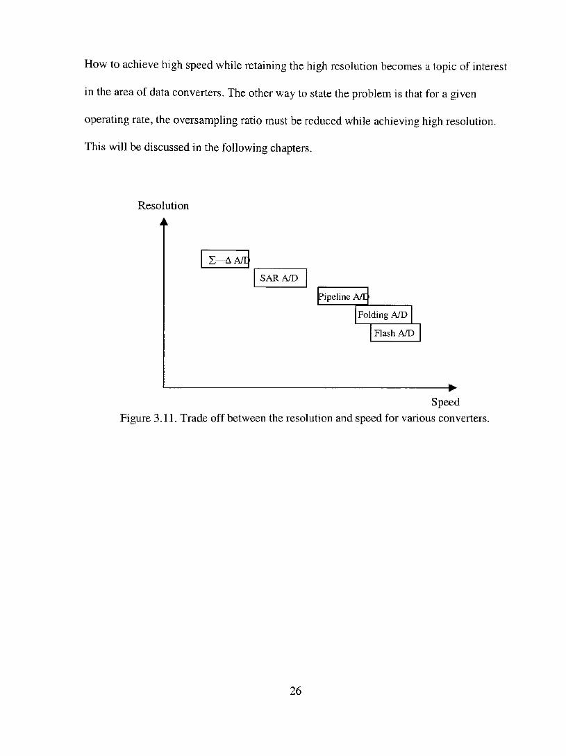
How to achieve high speed while retaining the high resolution becomes a topic of interest
in the area of data converters. The other way to state the problem is that for a given
operating rate, the oversampling ratio must be reduced while achieving high resolution.
This will be discussed in the following chapters.
Resolution
Z—AA/r
SARA/D
Pipeline A/E
Folding A/D
Flash A/D
Speed
Figure 3.11. Trade off between the resolution and speed for various converters.
26

CHAPTER 4
MULTI-BIT SIGMA-DELTA MODULATOR BASED ADC
4.1 Overview
As mentioned in the previous chapters, the signal bandwidth to be converted in a
sigma-delta modulator based analog-to-digital converter is limited by the maximum
frequency at which the converter can be operated and its oversampling ratio. Therefore,
sigma-delta modulator analog-to-digital converters have been used largely in audio
frequency ranges. To increase the signal bandwidth while retaining the high resolution,
either the order of the modulator or the resolution, hence the number of bits, of the
intemal coarse quantizer needs to be increased. These methods lead to a reduction in the
oversampling ratio for a given resolution, and thus an increase in the signal bandwidth
that can be converted. The dynamic range and the resolution of the modulator is a
function of the number of bits of the intemal quanfízer and the order of the modulator.
For a given operating frequency and a given oversampling ratio, either the order of the
modulator or the number of bits of the coarse quantizer or both needs to be increased to
achieve high resolution.
Increasing the modulator order makes it more prone to component inaccuracies
and system instability. Moreover, increasing modulator order requires a more
complicated decimation filter to remove the out of band quantization noise. The use of a
muUi-bit quantizer offers some attractive features. For every additional bit in the intemal
quantizer, an improvement of 6 dB occurs in the output signal-to-noise ratio. Thus, for a
27
given resolution, the use of a multi-bit quantizer can reduce the oversampling rafío. In
addition, the same decrease in the quantization error that improves resolution also relaxes
the requirements on the design of decimation filter that removes out-of-band quanfízation
error. It also facilitates the design of the high-order sigma-delta modulator feedback
loop, as the quatization noise becomes less signal dependent (i.e., more white) and the
unstable low-frequency oscillation (limited cycle), due to the overload of a single-bit
quantizer, is mitigated by the use of more quantization levels [2, 3]. However, the use of
an intemal multi-bit quantizer requires an intemal multi-bit digital-to-analog converter
(DAC) in the feedback path in a regular sigma-delta modulator. Unlike the single-bit
DAC, the use of a multi-bit DAC introduces nonlinearity errors (mostly distortion) due to
the mismatch of the components in the VLSI process in the system. Moreover, these
errors cannot be spectrally shaped. Thus, the linearity of the overall conversion system is
no better than the linearity of the intemal multi-bit DAC. Therefore, the overall resolution
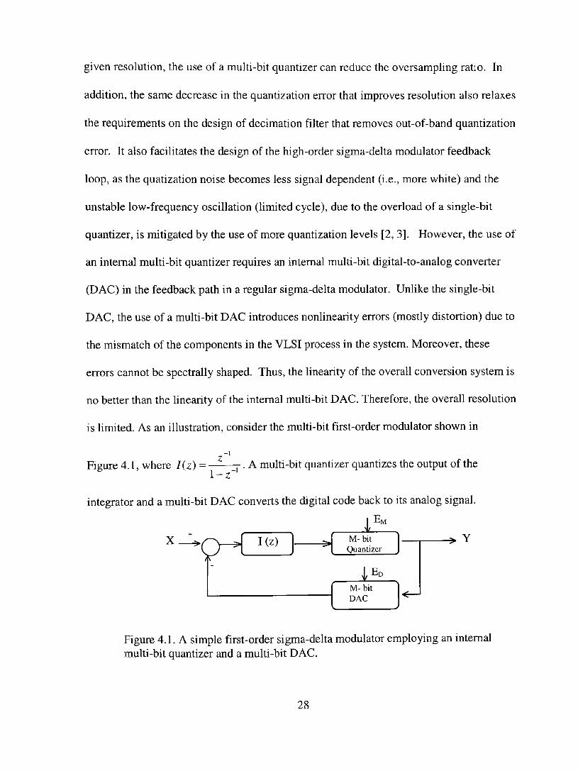
is limited. As an illustration, consider the multí-bit fírst-order modulator shown in
Figure 4.1, where I{z) l-z -1
A multi-bit quantizer quantizes the output of the
integrator and a multi-bit DAC converts the digital code back to its analog signal.
I EM
X ^ ^ ^ ^ T (z) =J M- ^^ n 1 > Y ' ^ ^ ) ^
\
I(z) M-bit Ouantizer
iE. M-bit DAC
Figure 4.1. A simple fírst-order sigma-delta modulator employing an intemal multi-bit quantizer and a multi-bit DAC.
28

The output of such a modulator can be written as follows
Y^Xz'^E^{\-z-')-E^z-\ (4.1)
where X is the input signal , EM and EQ are the multi-bit quantization error and the
nonlinear error introduced by the multi-bit DAC, respectively. E^ is - ^ ^ t h a t of a
single-bit quantizer, thus the quantization error appearing in Y is reduced by a factor of
2^"^. However, EM is spectrally shaped, but ED appears in the output in its entirety
without spectral shaping in this case.
Achieving high linearity requires precisely matched components to implement the
multi-bit DAC. The matching is usually limited depending on the process used. For a
sigma-delta modulator implemented in a switched capacitor circuit, the capacitor
matching in a typical CMOS process is roughly limited to 10 bits. To circumvent the
requirement for high precision elements, it is possible to exploit the fact that the number
of output levels is still small so that some techniques, including component trimming,
dynamic element matching, interpolation, and digital error correction or calibration, have
been used to compensate the mismatches [3, 13, 14, 15, 16, 17, 18, 19]. However, the
component trimming requires more expensive facilities and more testing time, thus
increasing the overall cost. The digital error correction and the dynamic element
matching lead to the use of more complicated digital circuitry in the implementation of
multi-bit DACs. The use of digital error correction requires memory elements and the
associated digital circuitry to cahbrate the multi-bit DAC error [13, 14]. Moreover, the
29
use of dynamic element matching techniques, such as data weighted averaging [15, 16],
element randomization [3], element rotation-barrel shifter [3], individual level averaging
[18, 19], double index averaging [17], etc, achieves only fírst order noise shaping
functions for mismatches of the components and also suffers from tone problems in some
algorithms. The first order noise shaping may not be suffícient for a low oversampling
ratio application (high speed) if a typical CMOS process is used.
The problem can also be alleviated by the design of system architectures; for
example, utilizing a dual-quantization cascade ADC topology (regular MASH structure)
[20] or a dual-feedback single-path ADC topology [21] can spectrally shape the multi-bit
DAC errors. The modulator described in [20] includes two or more stages, the first stage
is a single-bit second-order modulator employing the Candy structure. The second stage
or the last stage is a multi-bit first-order modulator. Between the stages interstage gain
scaling is used to avoid overloading and to extend the dynamic range. Thus, the multi-bit
DAC can be spectrally shaped by the shaping function of the first stage or previous stage
of themodulator.
4.2 Multi-bit sigma-delta modulator without multi-bit DAC
System stmctures that avoid the use of a multi-bit DAC in the feedback path of
the modulator shown in Figure 4.2(a) was fírst suggested by Leslie and Singh in 1990
[22]. This stmcture employs a multi-bit quantizer in the forward path; only the most
signifícant bit (MSB) is used to drive the feedback path. Thus, only a single-bit DAC is
applied on the feedback path that is inherently linear. The equivalent stmcture consists of
30
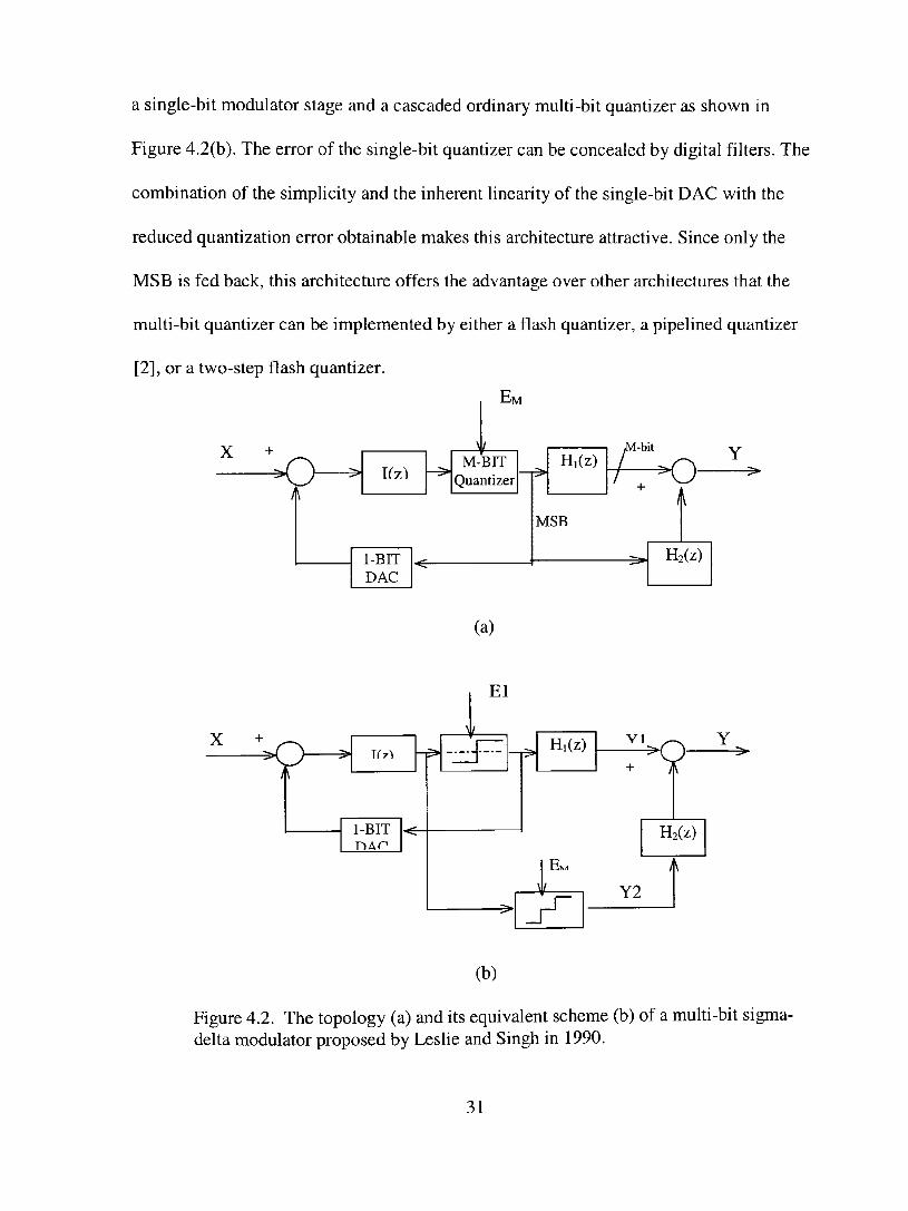
a single-bit modulator stage and a cascaded ordinary multi-bit quantizer as shown in
Figure 4.2(b). The error of the single-bit quantizer can be concealed by digital filters. The
combination of the simplicity and the inherent linearity of the single-bit DAC with the
reduced quantizafíon error obtainable makes this architecture attractive. Since only the
MSB is fed back, this architecture offers the advantage over other architectures that the
multi-bit quantizer can be implemented by either a flash quantizer, a pipelined quantizer
[2], or a two-step flash quantizer.
EM
X
< >
Y
^ f(z) M-BIT
Quantizer
1-BIT DAC
H,(z)
MSB
M-bit
o-
H2(Z)
(a)
X + o > Try-l
1-BIT r»Ar
El
Hi(z)
\L
VI Y -KJ > + T
H2(Z)
Y2
(b)
Figure 4.2. The topology (a) and its equivalent scheme (b) of a multi-bit sigma-delta modulator proposed by Leshe and Singh in 1990.
31

Assuming that the integrator I{z) = ^^and the digital fílter //,(c) = Iand 1-z
Hj^z)^^- z-\ the output of the single bit modulator Y] and the multi-bit quantizer Y2
are given by linearized analysis as
K (Z) = X{z)z-' + E, {z){l - z-') and (4.2)
Y,{z) = {X{z)-Y,{z))^^ + E^{z). y-z
(4.3)
where E] and EM are the quantization errors of the single-bit and multi-bit quantizers.
Therefore,
y(z) = X(z ) z - '+£^ ( l - z - ' ) (4.4)
X
^ > I(z)
Y Hi(z)
'M + F I *—
Y H2(Z)
Figure 4.3. The system topology proposed by Kinyua and Chao (1997) and Brooks, Robertson and Kelly (1997).
32

Modifications of this topology that use the concept of multi-step quantizer or
pipelined quantizer to implement the multi-bit quantizer have been made [23, 24]. The
implementation in silicon has proved the feasibility of the architecture [24]. Shown in
Figure 4.3, the quantization error of the first stage enters the second stage in which a
multi-bit quantizer is used in the forward path without the feedback loop, thus no DAC
error is introduced. While the output F remains the same as in Equation 4.4, the muhi-bit
quantizer is now used to quantize the error of the single bit (or first-step) quantizer. The
input range to the multi-bit quantizer is reduced. Similarly, the single-bit (or first-step)
quantization error is cancelled by the use of digital filters.
>m7 H5(Z)
Figure 4.4.The system employing interstage scaling concept proposed by Chandrasekaran and Chao (1997).
33

An architecture which apphes the concept of mterstage gain scaling to the
cascading of such systems has been proposed [25]. Figure 4.4 shows the structure where
the multi-bit quantization error of the first stage, EMI, is scaled back to full scale by gain
factor K and enters into the sigma-delta modulator of the next stage. If the digital filters
H,{z) = z-"\H^{z) = \-z-\H,{z) = z-''\H,{z) = l-z-\H,{z) = z-'"'''\2iná
H(,{z) = 1 - z"' are selected, the overall output can be described as
r(z) = X ( z ) z - ^ + ( l - z - ' ) ^ ^ , (4.5)
where A is the total delay of the modulator that is dependent upon how the multi-bit
quantizer is implemented. The topology provides high-order noise shaping and the
quantization noise is further reduced by a factor of K.
4.3 Other multi-bit sigma-delta modulator systems
Other multi-bit systems that lead to high resolution and high speed are proposed
in this thesis. In Section 4.3.1, the multi-bit sigma-delta modulator with multi-bit DAC
error cancellation is described. Following is a multi-bit sigma-delta modulator with inter-
stage feedback. The topology that spectrally shapes the pole errors with digital
requantization is discussed in Section 4.3.3.
4.3.1 Multi-bit sigma-delta modulator ADC with multi-bit DAC error cancellation
An altemative system topology that completely eliminates the multibit DAC error
is proposed [26]. In such a system, a multi-bit DAC is used in the feedback loop of the
34

modulator of the second stage and its output is fed back to the main modulator in the fírst
stage and the DAC error is cancelled by digital fíltering. System level simulation results
showing near ideal performance are also included.
The basic structure of the proposed multi-bit modulator is shown in Figure 4.5.
Basically, it is a two-stage system. The fírst stage is a modulator with a single-bit
quantizer and single-bit DAC that is inherently linear. The second stage has an intemal
multi-bit quantizer and a multi-bit DAC in the feedback path.
X A ^ ^ 1-bit Quantizer
s 1-bit DAC
^ 'M Hi(z)
^
— I
cM^^ M-bit Quantizer
M-bit DAC
H2(z)
Figure 4.5. The proposed system. I](z) and I^^z) are integrators. H](z) and H^^z) are digital filters.
As shown in Figure 4.5, the quantization error Ej of the single-bit quantizer of the
first stage enters the second stage multi-bit sigma-delta modulator as input, similar to the
regular MASH structure. However, this system differs from the regular MASH structure
in that the signal immediately after the multi-bit DAC is also fed back to the main
modulator and is spectrally shaped. As a result, the quantization error Ei of the single-bit
35

quantizer and the error ED due to nonidealities when implementing the multi-bit DAC can
be cancelled completely by applying digital filters Hi(z) and H^^z). In the regular MASH
architecture, since there is no feedback path from the second stage to the first stage, the
multi-bit DAC error in the second stage is only spectrally shaped by the shaping function
of the first stage [20].
For simplicity, it is assumed that the modulators in the first stage and second stage
-1 z
are of first order, such that f {z) = I^ {z) — - The digital outputs of the proposed 1-z
system can be expressed by the
Y](z) = X(z)z' + E](l-z')' -EM(l-z')'-ED(l-z'f (4.6)
and
Y2(z)= E]Z^-^EM(1-Z') EDZ' (4.7)
where Y](z) and Y^^z) are the digital outputs of the modulator in the fírst and second
stage, respectively, and EM is the quantization error of the multi-bit quantizer of the
second stage. If the digital fílters used have the transfer function such that H](z)=z' and
H2(z)=(l-z^f, the resulting output of the overall modulator is
Y(z) = Y](z)H](z) - Y2(z)H2(z) = X(z)z'-EM(I-Z')^- (4.8)
The multi-bit quantization error EM is spectrally shaped by the second order shaping
function, (l-z^)^, as expectedfor a second-order modulator. The quantization errorE] of
the fírst stage and multi-bit DAC error ED of the second stage are completely cancelled.
The proposed system topology has been simulated in SMULINK and MATLAB
for a system that consists of a fírst-order modulator in the fírst stage and a 4-bit fírst-order
36
modulator in the second stage. The system is simulated with an 8kHz sinusoid as input,
an oversampling ratio of 64, and a sampling frequency of 2.62144MHz. For
demonstration purpose, the multi-bit DAC error is assumed to be a wideband noise with
its amplitude bounded by [- A/2, +A/2], where A is the step size of the multi-bit
quantizer. In comparison, the regular MASH topology with both ideal and nonideal DAC
is also simulated with the same settings. The power spectral density (PSD) and signal-to-
noise ratio (SNR) are calculated to evaluate the performance. The simulation results of
the proposed system and that of the regular MASH structure are given in Figures 4.6 and
4.7. For comparison purposes, the simulation result of a regular MASH with ideal multi-
bit DAC is also included in Figure 4.6. It is shown that the noise floor of the proposed
system is similar to that of the regular MASH structure with ideal DAC and is much
lower while the SNR is about 15 dB higher than that of the regular MASH structure with
nonideal DAC. The same order of improvement in dynamic range is also observed. These
results demonstrate that the multi-bit DAC error of the second stage is completely
cancelled in the proposed system.
37

P . S . D ( d B )
c
0
5 0
0 0 " _ , _ — A
0 5 1 1 .5 2 2
--
0 .5 1 .5
1 1 .5 F r e q u e n c y ( H z )
2 . 5 X 10
2 5 x 1 0
2 . 5 X 1 0
Fighure 4.6. Baseband power spectral density of the output of the proposed structure (top figure), the regular MASH topology with ideal multi-bit DAC (middle figure) and with nonideal multi-bit DAC (bottom figure) in the feedback loop of the second stage.
100 Comparison with regular MASH system
-100 -80 -60 -40 -20 Input amplitude (dB)
Figure 4.7. SNR for the proposed structure (upper curve) and that of the regular MASH topology with nonideal multi-bit DAC (lower curve) as a function of input signal level.
38

4.3.2 Multi-bit sigma-delta modulator ADC with interstage feedback
In order to improve the noise shaping function, a topology employing interstage
feedback is introduced [27]. The quantization error due to the multi-bit quantizer is fed
back to the modulator in the main stage to allow spectral shaping beyond that achieved
by the main modulator with the Candy structure. The topology combines the advantage
of high order noise shaping and the pipeline concept to achieve high resolution and high
speed A/D conversion. The proposed architecture is shown in Figure 4.8, where the main
stage is a modulator with a 1-bit quantizer and a multi-bit quantizer realized by a pipeline
system in the second stage. I(z) is integrator and Hi(z) and H^^z) are digital filters. The
blocks inside the dash line are the pipeline quantizer.
X ^ ^ I(z) ^ < V ^ Y
^ Hi(z) ^
*É, ôî Z' Y
HD F(z)
T 7 - I
H2(Z)
Figure 4.8. The multi-bit sigma-delta modulator employing interstage feedback.
The quantization error Ei generated by the single-bit quantizer is canceled by the
digital filters Hi(z) and H2(z), while the multi-bit quantization error Em is fed back to the
39
main modulator and noise shaped. Since the muki-bit quantizer is assumed to be
implemented in a one bit per stage pipeline system, it results in a one bit DAC that is
inherentiy linear in each stage of the pipehne system.
For simplicity, it is assumed that the main stage is of fírst order, I(z)=z^/(l-z^).
The digital outputs Y](z) and Y^^z) of the proposed system are expressed by
Y](z) = X(z)z' -h (l-z')E](z) + (l-z')F(z)EJz) (4.9)
and
Y2(z) = E](z) z''-^ EM (4.10)
where F(z) = 1, H](z) = z'", H^íz) = I z\ and m is the number of unit delays required
for implementing the multi-bit quantizer. The resulting output Y(z) of the overall
modulator becomes
Y(z) = Yj(z)H](z)-Y2(z)H2(z)
= X(z)z-^"^'^ (1 z')(l - z^EUz). (4.11)
The multi-bit error is noise shaped by the function (1 z'^)(l z'^) instead of (1 z'^). If
the main modulator is of second order, then F(z) = (2 z'"), H](z) = z'", H^^z) = (1 - z'^/,
and the overall output can be shown as
y(z)=X(z)z-^'"^'^ (1 z'')\l z"'fEm(z). (4.12)
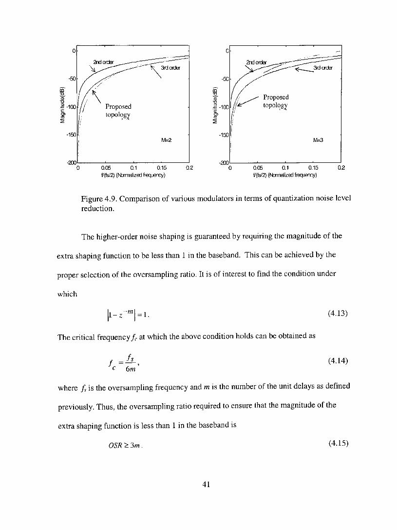
For a second-order main modulator, the multi-bit quantizer error can be shaped well
beyond the second order by an extra shaping factor (1- z'"^) . The effect of the additional
shaping factor can be seen in Figure 4.9. In the low-frequency end, even more reduction
of the quantization noise level is observed if we compare it with the third-order noise
shaping.
40
-200
M=2
0.05 0.1 0.15 ^(fs/2) (Normalized frequency)
0.2 -200
M=3
0.05 0.1 0.15 f (fe/2) (Normalized frequency)
0.2
Figure 4.9. Comparison of various modulators in terms of quantization noise level reduction.
The higher-order noise shaping is guaranteed by requiring the magnitude of the
extra shaping function to be less than 1 in the baseband. This can be achieved by the
proper selection of the oversampling ratio. It is of interest to fínd the condition under
which
l-z = 1 . (4.13)
The critical frequency/c at which the above condition holds can be obtained as
f - - ^ 6m
(4.14)
where / , is the oversamphng frequency and m is the number of the unit delays as defíned
previously. Thus, the oversampling ratio required to ensure that the magnitude of the
extra shaping function is less than 1 in the baseband is
0SR>3m. (4.15)
41

When compared with the results of the modulator described in [22] and [23], the
proposed topology gives a smaller error providing that the oversampling ratio is greater
than a critical value 3m. The condition is easy to satisfy. For example, only 3 unit delays
are required to implement a 6-bit pipeline quantizer in a 1-bit per stage structure. This
means OSR >9 is required. In the case of 0SR=9, the signal-to-noise ratio can be
improved by 4.5dB and 9dB due to the additional shaping factor (l - z'"") and (l - z"'" f,
respectively. Since the feedback error is the error of a multi-bit quantizer that is
relatively small, the instability problem can be mitigated in the main modulator.
The proposed system topology has been simulated in SEMULINK and MATLAB.
For a system whose main modulator is of second order and has a 5-bit quantizer in the
feed-forward path, the proposed system is simulated with a lOkHz sinusoid as input, an
OSR of 64, and a sampling frequency of 2.62144MHz. In the simulation, a one bit and
one unit time-delay per stage pipeline multi-bit quantizer is assumed. For the purpose of
comparison, the system given in [23] and [24] is also simulated with the same settings.
The power spectral density and signal-to-noise ratio of the proposed system and the one
presented in [23] and [24] are given in Figures 4.10 and 4.11, respectively. It is shown
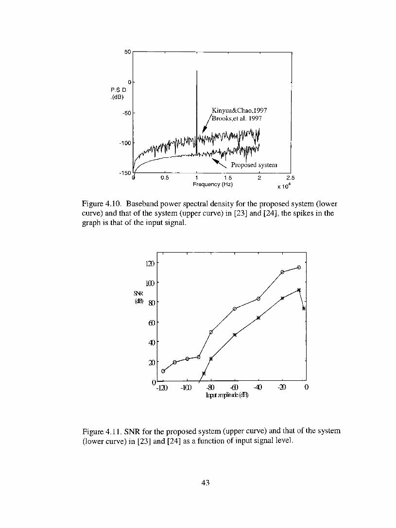
that the noise floor of the proposed system is much lower while the SNR is about 25dB
higher than that of the system described in [23] and [24]. The same order improvement in
dynamic range is also observed.
42
50
P.S.D .(dB)
-50
-100
-150
Kinyua&Chao,1997 'Brooks,et al. 1997
Proposed system
1 1.5 Frequency (Hz) x10
2.5 4
Figure 4.10. Baseband power spectral density for the proposed system (lower curve) and that of the system (upper curve) in [23] and [24], the spikes in the graph is that of the input signal.
120 •100 -80 -60 ^ lripUanpiitu[fe(dB)
20 0
Figure 4.11. SNR for the proposed system (upper curve) and that of the system (lower curve) in [23] and [24] as a function of input signal level.
43

4.4.3 Multi-bit sigma-delta modulator with high-order noise-shaped integrator leakage
The multi-bit modulator system systems discussed so far are two-stage systems.
Like the MASH structure, the cancellation of the errors in the first stage depends upon
the matching between the analog filter and the digital filters applied. However, there are
mismatches between the digital filter and the analog circuits in practice; those errors
cannot be cancelled completely. Usually, these residual errors (namely, the integrator
leakage) limit the performance that the systems can achieve. For switched-capacitor
implementation of analog integrators, the mismatches in capacitors and the finite gain
and bandwidth of the operational amplifier cause gain and pole errors in the integrator
(see Appendix A).
Considering the structure of Figure 4.2(a), and assuming that
(l-a)z-^ I{z) ^— ——, where a, |3 are gain error and pole error, respectively, then the final
l-{l- ^)z
output will be Y{z) = X{z)-^ E,{z)a{l- z-') + E,{z)j3z-' + E^{1- z-'). (4.16)
While the gain error a is fírst-order shaped, the pole error p appears in the output
in its entirety. Therefore, similar to the MASH structure, the achievable performance is
limited by the idealities. The pole error of the integrator can be alleviated by an op-amp
gain compensated integrator [28, 29, 30, 31, 32, 33, 34], or digital calibrations [35, 36].
However, the gain error due to the capacitor mismatches in the switched capacitor
integrator with a compensated op-amp gain cannot be improved. The gain error becomes
the major limitation factor for low oversampling ratio even if it had been first order
44
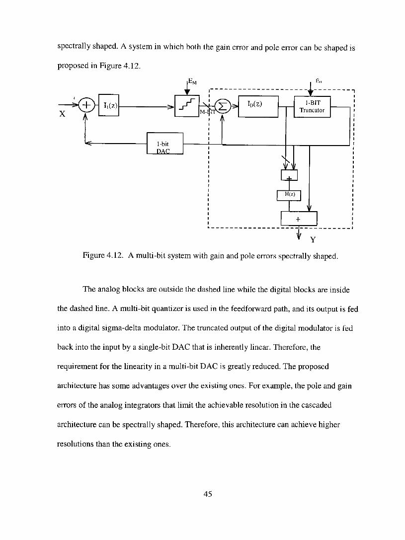
spectrally shaped. A system in which both the gain error and pole error can be shaped is
proposed in Figure 4.12.
X ^ I , (
Figure 4.12. A multi-bit system with gain and pole errors spectrally shaped.
The analog blocks are outside the dashed line while the digital blocks are inside
the dashed line. A multi-bit quantizer is used in the feedforward path, and its output is fed
into a digital sigma-delta modulator. The truncated output of the digital modulator is fed
back into the input by a single-bit DAC that is inherently linear. Therefore, the
requirement for the linearity in a multi-bit DAC is greatly reduced. The proposed
architecture has some advantages over the existing ones. For example, the pole and gain
errors of the analog integrators that limit the achievable resolution in the cascaded
architecture can be spectrally shaped. Therefore, this architecture can achieve higher
resolutions than the existing ones.
45

The output of the system can be obtained by hnearized model analysis as
Y,{z)= X{z){\- a) - E^{z){\- z-')z-W- a){\- Pz-' - az-') (4.17)
+ E^{z){\-z-' + A Xl + y^r' +az-')
and
Y.Sz) = Y,{z) + E^{z){\-z-'). (4.18)
The overall output is:
Y = Y,-H{z)E^{z)
X{z)-E^a{\-z-')^-E^{\-z-')/k-'+E^{\-z-'). (4.19)
Note that ED here is similar to E] in Equation 4.16. Comparing Equation 4.16 and
Equation 4.19 shows that the gain error is second-order shaped and the pole error is fírst-
order shaped in the new architecture. However, the multi-bit quantizer cannot be
implemented by a pipelined structure.
The system can be extended to high order as shown in Figure 4.13, where I](z)
and l2(z) are analog integrators, IDCZ) is a digital integrator, and H(z) is the digital filter.
AIso, EM is the multi-bit quantization error, EMD denotes the error caused by the multi-bit
DAC, and ED is the digital truncation error.
Without loss of generality, we further assume that the second integrator I^^z) is an
ideal integrator and the digital filter H{z) - (1 - z~^)" • The overall output can be derived
as
1 \ 2 77 _ /9 . / 1 _ - l \ _ - l Y = X{\-a)-Ej,*a*{\-z-'y-E^*l3*{\-z-')z
+ E^A\-z-') + E^*{\-z-\' (4.20)
46

X ( + ) - i,(z) - ( + ) - i2(z) - _ r ^ r< l^ '"*''
W EMD \ T
M-BIT DAC
1-BIT
DAC
\
i En
1-BlT Truncator
\
í H(z)
T
Figure 4.13. The extension of the system in Figure 4.12 to high order noise shaping.
The gain error a has been spectrally shaped to second order, and the pole error p
has been shaped to fírst order. The error caused by the multi-bit DAC has also been
spectrally shaped to fírst order. If the multi-bit DAC is implemented using dynamic
element matching, the multi-bit DAC error can be spectrally shaped to second order. The
interstage scahng concept can also be applied to the cascading of such systems in order to
achieve higher order modulators.
The proposed architecture has been simulated in MATLAB and SIMULINK for a
system consisting of a first-order modulator and a 5-bit intemal quantizer as shown in
Figure 4.13. The system proposed (also referred to as system I) is simulated with a 10-
kHz sinusoid as input and a samphng frequency of 2.62144 MHz. The amplitude is kept
47
at 0.5 and oversampling ratios (OSR) of 16, 64 and 128 are used to evaluate the
performance. In comparison, the system based on the architecture proposed by Leshe and
Singh (1990) (also referred to as system II) is also simulated with the same settings. The
power spectral density (PSD) and signal-to-noise ratio (SNR) are calculated for
comparison. The simulation results of the proposed system and the structure of Figure
4.2 are given in Figures 4.14 and 4.15. Figure 4.14 shows the power spectral density of
both systems assuming that both gain and pole errors are 0.01. It shows that the noise
floor of the proposed system (system I) is much lower than that of the system without
spectral shaping of the pole error (system II), particularly in the low-frequency range.
Figure 4.15 shows the effects of the gain error and pole error on the signal-to-noise ratio
(SNR) for both systems. The simulation results show that the integrator leakage error due
to the pole and gain error degrades the performance. For example, the SNR for the
system using the ideal integrator is 75dB at OSR=64, the SNR for system I (proposed
system) and system II are 74dB and 61 dB, respecfívely, when a=0.01 and p=0.01. Since
the pole error is first-order shaped in system I and is unshaped in system II, the integrator
R r o q u e n c y ( H z )
Figure 4.14. The power spectral density (PSD) of the output of both systems with both gain error and pole error are assumed to be 0.01.
48

100
80
^ 60
0) 40
20
*+: a=0.05 •o: a=0.0I
0SR=16
co
100
80
60
40
20
jf- V"
*+: a=0.05 •o: a=0.01
OSR=64
-4 -3.5 -3 -2.5 -2 pole error (loglO(beta)
-4 -3.5 -3 -2.5 -2 pole error (loglO(beta)
100
80
40 CO
20
• • * •
•
• OSR=
fa).
^ í-
= 128
*+ •o:
a=0.05 a=0.01
- \ - •
• * •
-4 -3.5 -3 -2.5 -2 pole error (loglO(beta)
(c)
-3 -2.5 -2 -1.5 -1 gain error (loglO(alpha)
(d)
Figure 4.15. The effects of gain and pole errors on signal-to-noise ratio for the proposed system (o, +) and the system (*, •) in [20].
leakage error due to pole error is greatly reduced. A SNR close to ideal performance is
achieved in this case by system I. The performance difference between system I and
system II is more obvious with the increase of oversampling ratio (Figure 4.15 (c)). To
illustrate the effects of gain error on both systems, no pole error is assumed and the
intemal quantizer of 7 bits is assumed. Since gain error is spectrally shaped in both
systems (Equations 4.19 and 4.16) and the effect becomes negligible at high OSR, the
low OSR is preferred in evaluating the effect. The gain error in system I is second-order
spectrally shaped while it is only first-order shaped in system II. The difference between
49

both systems can be seen in Figure 4.15(d). The simulafíon resuks clearly show that the
proposed system has less gain and pole error effects than those of the system without pole
error shaping.
50

CHPATER 5
ARCHITECTURE AND BEHAVIORAL SIMULATION
As stated in previous chapters, sigma-delta modulator converters achieve high
resolufíon while the speed is limited due to the nature of oversampling. Several attempts
have been made to extend the signal bandwidth to above IMHz with high resolution [24,
37, 38, 39]. It is of great interest to develop high-speed, high-resolufíon, sigma-delta
modulator analog-to-digital converters in many applications; for example, cable modem
applications such as digital subscribe lines [5, 38]. The performances of several published
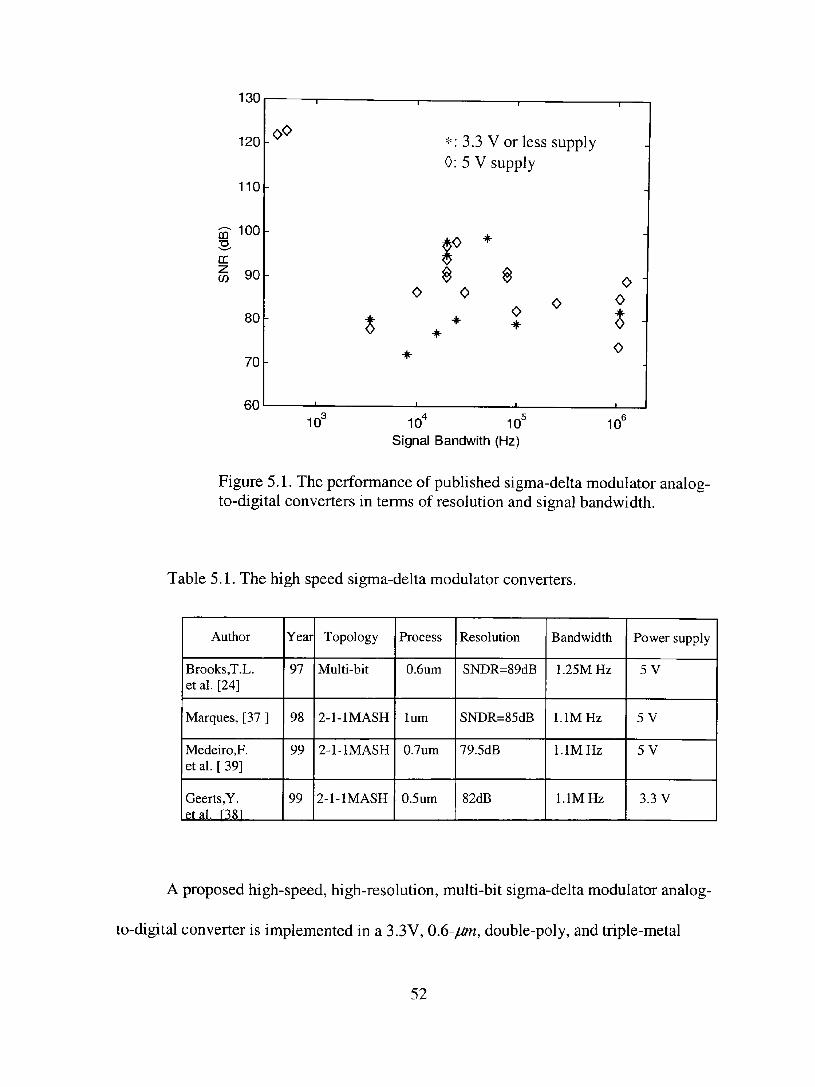
sigma-delta modulator analog-to-digital converters are compared in terms of resolution
and speed (the data are obtained from loumal ofSolid State Circuits). As shown in
Figure 5.1, the high speed achieved with high resolution is the result of the deeper
submicron technology. The converters are divided into two groups in terms of
architecture: single-bit sigma-delta modulators and multi-bit modulators. A close look
also reveals that such designs in the area of high-speed, high-resolufíon converters either
use multi-bit modulators [24] operating from 5 volts supply, or high order single-bit
modulators with MASH topology [37, 38, 39]. The key features of the published
converters based on the mulfí-stage are listed in Table 5.1.
51
120
110
m 100
fr Ú 90
80
70
60
1
oo
t
1
0
1
r
=í'-: 3.3 V or less 0: 5 V supply
r $
0
+
+
$
0 +
supply
0
r
-
0 " 0 $ •
0
1
10 10 10 Signal Bandwith (Hz)
10
Figure 5.1. The performance of published sigma-delta modulator analog-to-digital converters in terms of resolution and signal bandwidth.
Table 5.1. The high speed sigma-delta modulator converters.
Author
Brooks,T.L. etal. [24]
Marques, [37 ]
Medeiro,F. et al. [ 39]
Geerts,Y. etal. [381
Year
97
98
99
99
Topology
Multi-bit
2-1-lMASH
2-1-lMASH
2-1-lMASH
Process
0.6um
lum
0.7um
0.5um
Resolution
SNDR=89dB
SNDR=85dB
79.5dB
82dB
Bandwidth
1.25MHz
l . lMHz
l . lMHz
l . lMHz
Power supply
5 V
5 V
5 V
3.3 V
A proposed high-speed, high-resolution, multi-bit sigma-delta modulator analog-
to-digital converter is implemented in a 3.3V, 0.6-jum, double-poly, and triple-metal
52

CMOS technology using switched capacitor circuits. The ultimate objectives are to
demonstrate the novel architecture which employs the concept of interstage gain scaling
proposed in reference [25] and to achieve 16-bit resolution with signal bandwidth of
1.25MHz or beyond. Many design problems related to the low power supply that could
degrade the performance of the converter are studied at the system level as well as at the
circuit level. With the development of deeper submicron technology, the power supply is
reduced to 3.3V or less to reduce the high electrical fields in these technologies. Even in a
design with a 5V supply, sever constraints on the achievable performance of analog
circuits are imposed, it is a great challenge to design the same or higher level
performance with a reduced voltage supply of 3.3V [39]. For example, one of the
difficulties is that the reduced supply decreases the intemal signal swings and the
overdrive voltage for the switches of the switched-capacitor circuits.
5.1 System architecture
The proposed system architecture extends the inter-stage scaling concept given in
[25] (also shown in Figure 4.4). Basically, it is a multi-stage sigma-delta modulator
structure. The inter-stage scaling concept used in the pipeline is applied to bring the
residue of previous stage back to the full scale. As a result, the single-bit quantization
errors are cancelled and the multi-bit quantization error is further reduced when digital
filters are used.
53
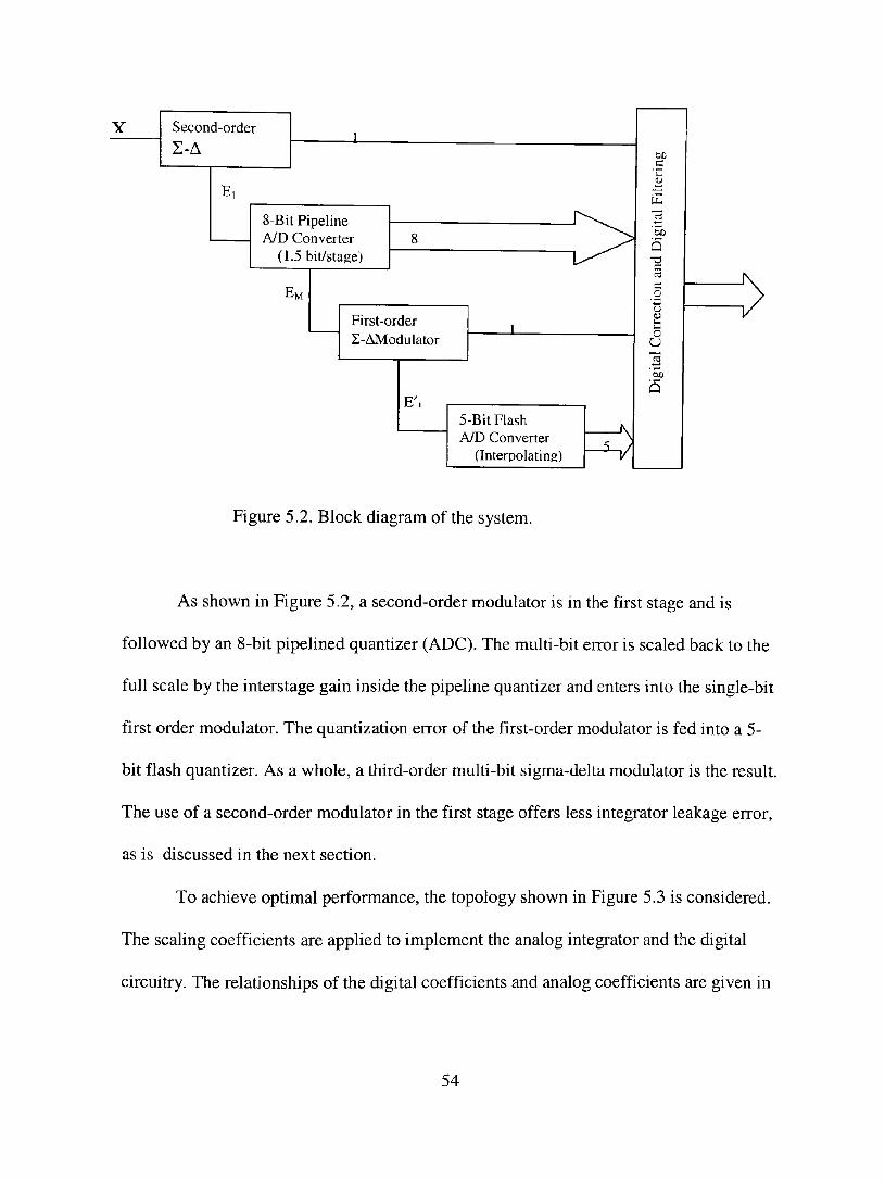
Second-order
S-A
8-BitPipeline A/D Converter
(1.5 bit/sta^e)
First-order S-AModulator
E', 5-Bit Flash A/D Converter
(Interpolating)
'ôíj
5 C cd
C
<u u. u. O
U
'ûÛ
5
Figure 5.2. Block diagram of the system.
As shown in Figure 5.2, a second-order modulator is in the first stage and is
followed by an 8-bit pipelined quantizer (ADC). The multi-bit error is scaled back to the
full scale by the interstage gain inside the pipeline quantizer and enters into the single-bit
first order modulator. The quantization error of the first-order modulator is fed into a 5-
bit flash quantizer. As a whole, a third-order multi-bit sigma-delta modulator is the result.
The use of a second-order modulator in the first stage offers less integrator leakage eiror,
as is discussed in the next section.
To achieve optimal performance, the topology shown in Figure 5.3 is considered.
The scaling coefficients are applied to implement the analog integrator and the digital
circuitry. The relationships of the digital coefficients and analog coefficients are given in
54

Table 5.2. The following considerations are used to select those coefficients. Firstly, the
level of the signals transferred from the previous stage to the next one must be small
enough to avoid overioading or saturation. Secondly, the output swing of every integrator
must be physically available. Thirdly, the peak input signal level is large enough to
achieve the required resolution without limitation by the intrinsic thermal noise or kTIC
noise. For a second-order modulator without scaling such that /j {z) = — and \- z
z-' h (z) = zr, the required output swing of the second integrator is at least four times
\-z
the reference voltage [2]. Hence, the peak input signal level is not to exceed 1/4 of the
output swing of the integrator. This is very difficult for a sigma-delta modulator
implemented with a low power supply because of the intrinsic noise of the circuits.
However, if the scaling coefficients are applied to both integrators such that
p 2 Z ^\(z) = — ^ ^ and I^iz)^—^—TT. wherebothgy andg^ are less than l,for agiven
\-z \-z
output swing of the integrator, the peak signal level is increased by a factor of . The
larger the peak input signal level, the larger the dynamic range. However, the nonlinear
errors of the later stages are also magnified by the same factor that limits the achievable
dynamic range. Therefore, it is possible to achieve the optimal performance with
properiy chosen coefficients. The digital filters H](z). H^^z) and Hs^z) are determined
accordingly such that H^{z) = \, H^{z) = {\-z-^j and H^{z) = \-z-^ canceloutthe
quantization noises of the first three stages. The overall output ycan be derived as
55
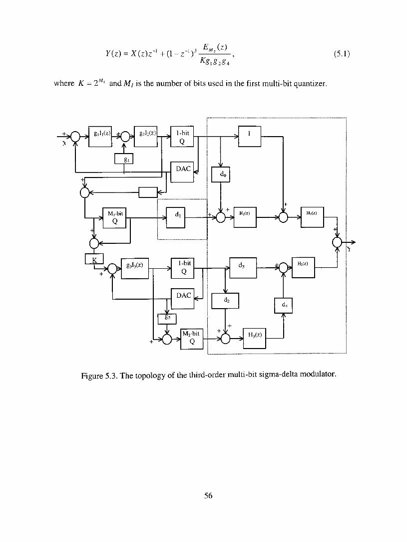
Y{z) = X{z)z~'+{\-z-'?-^^ Kg.g.g.
(5.1)
- O ^ i where K = 2 ' and Mj is the number of bits used in the first muhi-bit quantizer.
_jj^r\^ giii(z) ^r\, gsWz)
5
1-bit
Q
DAC
M|-bit
Q
i ^
g3l3(z) 1-bit
Q
DAC
g5
< > M2-bit
Q < > ^ H3(Z)
^ « < ' — > ( 5 - ^ »•<
^
H2(Z)
C ^
Figure 5.3. The topology of the third-order multi-bit sigma-delta modulator.
56
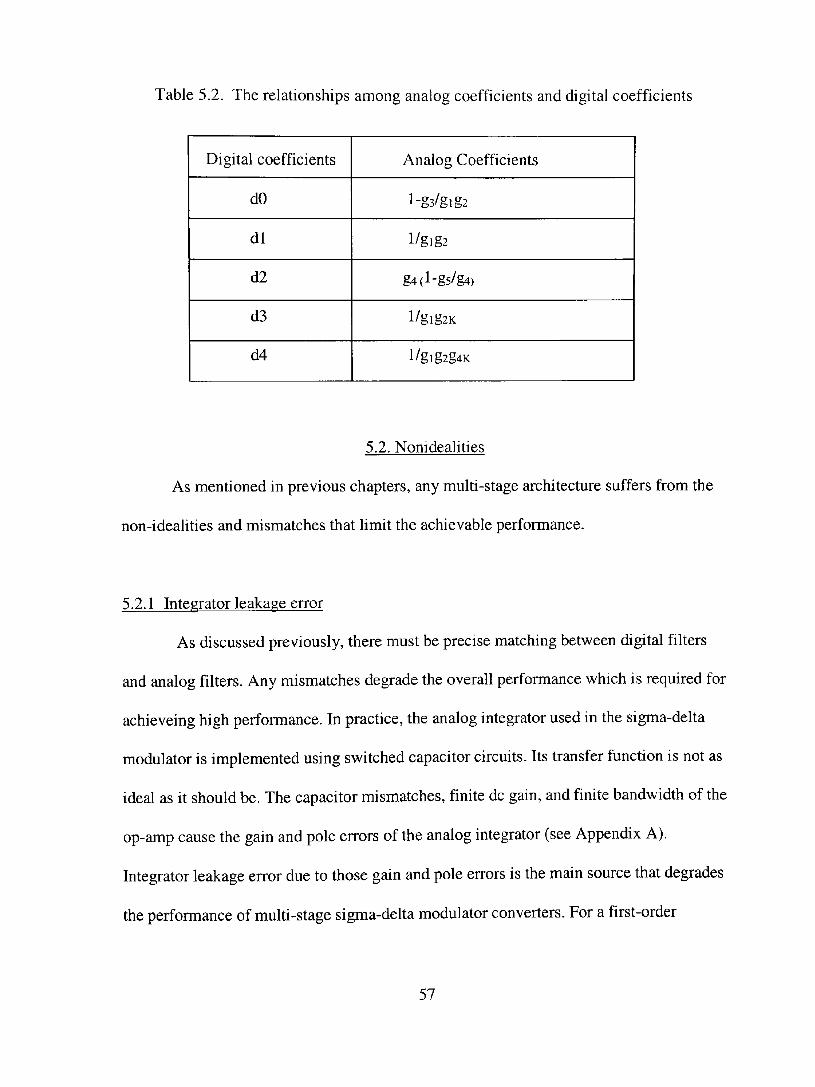
Table 5.2. The relationships among analog coefficients and digital coefficients
Digital coefficients
dO
dl
d2
d3
d4
Analog Coefficients
l-g3/glg2
l/glg2
g4(l-g5/g4)
l/glg2K
l/glg2g4K
5.2. Nonideahties
As mentioned in previous chapters, any multi-stage architecture suffers from the
non-idealities and mismatches that limit the achievable performance.
5.2.1 Integrator leakage error
As discussed previously, there must be precise matching between digital filters
and analog filters. Any mismatches degrade the overall performance which is required for
achieveing high performance. In practice, the analog integrator used in the sigma-delta
modulator is implemented using switched capacitor circuits. Its transfer function is not as
ideal as it should be. The capacitor mismatches, finite dc gain, and finite bandwidth of the
op-amp cause the gain and pole errors of the analog integrator (see Appendix A).
Integrator leakage error due to those gain and pole errors is the main source that degrades
the performance of multi-stage sigma-delta modulator converters. For a first-order
57

modulator, the gain error is first-order spectrally shaped while the pole error is not [2, 3]
(also refer to Equation 4.16).
A second-order modulator is used in the first stage to reduce the integrator
leakage errors. Considering the topology of Figure 3.8 (Candy's structure), and assuming
^~^l A j r ^ iX-OCi)^ that the integrator transfer function /, (z) = and U iz) = 1-(1-A)z"' \-{\-fi,)z-'
then the output Y can be derived as
Y{z) = X{z)z'' +E,{z){\-z-'f +E,{z){/3,-^ P,){\-z-')
-E,{z){a,+a^){\-z-'fz''-E,{z)a^{\-z''fz-'
where ai and 0C2 are the gain error, and pi and |32 are the pole errors of the integrators.
The last three terms are the integrator leakage errors due to gain and pole errors. The gain
errors appearing in the fourth and fifth terms are second-order or third-order spectrally
shaped; the pole errors are first order spectrally shaped. Therefore, this implementation
offers less sensitivity due to nonidealities than the one using first-order modulators in the
first stage [25]. With ai=a2=0.1%, pi=(32=0.01%, and an oversampling ratio of 16, for
instance, the noise level due to the integrator leakage error is estimated to be about
-105dB which is well below the noise level specifications of -96dB, for 16-bit
resolutions.
5.2.2 Multi-bit quantizer and the nonidealities
Two types of multi-bit quantuzer are used in the system, the pipeline 8-bit analog-
to-digital converter and 5-bit flash analog to digital converters. Numerous factors affect
58
the performance of the multi-bit analog-to-digital converters. Among them, offset of the
comparators and capacitor mismatches are the main factors affecting the hnearity and
resolution, provided that the gain and bandwidth of the op-amp are large enough.
Usually, comparators are used to implement the coarse quantizer. Its offset due to random
device mismatch is the dominant error source. A dynamic latch with preamplifier giving
low offset is considered in this design. This offset can be digitally corrected if the
redundancy-sign-bit scheme is used (see Appendix B). The capacitormismatches of the
gain stages become the dominant error sources in such pipeline analog-to-digital
converters.
5.3 Svstem simulation
The system is simulated in SIMULINK and MATLAB. In the behavioral
simulation, the gain of the operational amplifiers used to implement the integrator and the
gain stage in the pipeline is assumed to be 78dB. The mismatch of the capacitors is
assumed to be 0.2% in the first stage (second stage of modulator) and 0.5% in the
pipeline stage and thereafter. The offsets in the comparators are assumed to be distributed
in the range of [-30mV, 30mV]. The full scale of the reference voltage is set to be L6V.
In the simulation, different coefficients are used. Analog coefficients are chosen such that
g]=0.5, g2=0.5, g3=0.25, g4=0.5 and g5=0.5. The digital coefficients can be determined
accordingly by the relationships given in Table 5.2. For a signal level of -6 dB (referred
to the reference voltage), the output probability densities are shown in Figure 5.4. The
maximum output swings of both integrators are less than 1.2 times that of the reference
59

voltage used. The peak signal-to-noise ratio of 98dB is achieved for an oversampling
ratio of 16. The power spectral density is shown in Figure 5.5.
0.06
0.04
0.02
n
-1 -0.5
^—. 1
0 Output/Reference
1
1
0.5
1
1 ^ '
1
1
—• •
-
-
0.06
0.04
0.02
n
-1
1
i
-0.5 0
Output/Reference 1
0.5
1
1
-0.5 0 0.5 Output/Reference
Figure 5.4. The integrator output probability density for a -6dB input signal
60

-50
-100
•150
xlO
-100-
-150
xlO
Figure 5.5. Power spectral density (PSD) of the sigma-delta modulator shown in Figure 5.3. PSD in the baseband is shown at the bottom.
5.4 Circuit specifications
To achieve 16-bit resolution with an oversampling ratio of 16, the gain of the op-
amp is no less than 78dB. Since incomplete settling affects the pole error of the integrator
(Appendix A), the settling accuracy must be at least good enough to give less pole error
than that of the op-amp gain. For 40MHz operation with two-nonoveriapping clock
phases, the required bandwidth is at least 198MHz forl6-bit settling accuracy assuming
61

that each clock phase is 9ns. The specifications of the circuits are summarized in Table
5.3 based upon the simulation results.
Table 5.3. The circuit specifications
Op-Amp
Dynamic Range
Comparator
Capacitor
Gain>78+(4-6)dB, Bandwidth>198MHz (16-bit seUling) Output swing>2V
Intrinsic noise (Thermal noise) < -96dB
Offset< 30mV
Mismatch<0.2% (9-bit) for the first stage
62

CHPATER 6
CMOS VLSIIMPLEMENTATION
The system described in Chapter 5 is implemented by switched capacitor circuitry
in a O.ô xm CMOS process. For switched capacitor implementation, capacitors,
operational amplifiers (op-amp), comparators and switches are the main building blocks.
The detailed design and simulation results are described in this chapter. In addition, the
implementation of the subsystems such as single-bit second-order modulator, pipeline
quantizer, single-bit first-order modulator, flash quantizer and the clock generator and the
system integration are also included in this chapter.
6.1 Capacitors
The accuracy of the integrator gain and the gain-of-two stages in the pipeline
ADC depend mainly upon the ratio matching of the sampling capacitors and the feedback
capacitors. For a gain stage implemented in switched capacitor circuits with a high open-
loop gain op-amp, the closed loop gain is mainly proportional to the ratio of the
capacitors (see Appendices A and B). Any capacitor mismatches cause analog gain error
that is not predictable. It causes a mismatch between digital gain and analog gain, thus
affecting the overall performance of the system. In the case of the integrator, the gain
error is mainly caused by the capacitor mismatches (Appendix A). Since the high open-
loop gain and wide bandwidth op-amp is possible, the gain error of the integrator is the
dominant limitation for low oversampling ratio. In addition to the capacitor matching, the
63
hnearity of the capacitor is also important. If the charge-voltage relationship is nonlinear,
such that the capacitance is dependent on the vohage across it, harmonic distortions
result, thus degrading the signal-to-noise plus distortion ratio. Therefore, capacitors of
good matching and good linearity are necessary for achieving high resolution. Of many
pairs of layers that can be utilized to implement capacitors, the poly-poly has the best
linearity, good matching and highest capacitance per unit area. The capacitors used in this
design are therefore poly-poly capacitors.
kT The choice of the size of the sampling capacitor is determined by — noise of the
sampling switches and by the op-amp driving capability. The larger the size of the
capacitor, the lower the thermal noise level (see Appendix D). However, the size of the
sampling capacitor is limited by the op-amp driving capability. The larger the capacitor,
the more capacitive load the op-amp drives. The large capacitive load will reduce the
bandwidth of the op-amp (to be discussed later). The maximum possible signal-to-noise
ratio associated with the sampling switch and capacitor in differential implementations
[40] is
max 4 kT SNR ^L^^^2fll^, (6.1)
where k is Boltzmann's constant, Vpeak is the peak input signal level, OSR is the
oversampling ratio, and Cs is the sampling capacitor. For an OSR of 16, an input of IV
ampHtude (2V peak-to-peak) and resolution of 16 bits, the required sampling capacitor is
calculated to be 4.4pf. If the peak input signal level is 1.2V the required sampling
capacitor becomes 3pf. In this design, the input samphng capacitor Cs is chosen to be
64

4pf. The capacitance sizes of the later stages are scaled down to reduce the power
consumption and the die area.
6.2 Operational amplifier
The operational amplifier (op-amp) is the heart of any switched capacitor circuit.
It determines the performance of the overall systems. For example, the gain and pole
errors of the integrator are govemed by the op-amp used. Three widely used topologies
are folded cascode, telescopic cascode, and two-stage op-amp. A two-stage op-amp is
used in this implementation.
The criteria used in choosing topology are output swing, gain and bandwidth.
The output swing or the linear output region of the op-amp used in the integrator limits
the peak signal amplitude, thus limiting the dynamic range. With a second-order
modulator, for instance, the output is approximately 4-5 times the value fed back by the
DAC element, which is 4-5 times the range of the input signal level [2]. Large output
swing is very important for low oversampling ratio and the high-resolution sigma-delta
analog to digital converters. The achievable signal-to-noise ratio might be hmited if the
intrinsic noise of the circuit is larger than the quantization noise. The output swing,
however, is limited because the transistors are stacked in cascode topology to achieve
high gain. For example, 4 transistors are usually stacked in the folded cascode topology
and 5 transistors are used in the telescopic cascode topology. All transistors should be
biased in the saturation region, the maximum linear output swing is estimated to be VDD
-4-^5 times VSAT. where VDD is the power supply voltage. In practice, the transistors are
65

set to be working in the deep saturation region such that ^5^7- is typically about 3 times
Vgs-Vr (about 0.4-0.5V) for proper operation. This may not be a severe problem for a
5V process. A typical value of 3-3.5V can be achieved in the folded cascode topology
for a 5V power supply. However, the power supply in modem processes goes to 3.3V or
below when the features continues to shrink. The limitation on output swing becomes a
major problem. AIso, the gain of the single stage op-amp, such as those op-amps in the
folded cascode or telescopic cascode structure, is typically 60-70dB, whích is not enough
for the required specifications given by the behavioral simulation. Although gain
boosting techniques can be used to improve the gain, they do not improve the output
swing. Another consideration is that the single stage op-amp is usually compensated by
the load capacitance that varies in different phases of the clock cycle. In one phase, the
compensation might be not enough to ensure stable operation. The settling time of the op-
amp changes from one phase to the other. The additional advantage of utilizing a two-
stage op-amp is that the dependence of the settling time on the load capacitance is less,
because the load capacitance does not affect the dominant pole significantly. Therefore, a
two-stage op-amp is preferred in the low voltage design to achieve large output swing
and high gain. Bandwidth may be reduced when compared to the single-stage op-amp;
however, wide bandwidth is possible by means of minimizing feature size and increasing
bias current.
66

6.2.1 Two-stage op-amp and design equations
6.2.1.1 Core circuit
The core circuit of a fully differential two-stage op-amp is shown in Figure 6.1. A
telescopic topology is used in the first stage, and the second stage, or output stage, is the
ordinary inverting amplifier. Cascode compensation other than MiIIer compensation is
applied to obtain wide bandwidth in this design [41, 42, 43]. The compensation capacitor
is connected from the output node of the second stage to the cascode node of the first
stage, thus the capacitor closes a feedback loop around a two-pole system. In the standard
MiIIer compensation technique, the capacitor is connected from the output node of the
second stage to the output node of the first stage; hence, it only closes a one-pole
feedback loop [42]. Another benefit is the improvement of the negative power supply
rejection [43]. Figure 6.2 shows the corresponding AC small signal model for half of the
circuits.
AVDD ]CPt<lC X
% e ^
M
Mio '^ y
te — ^ v ^
Z}[
Vbl
Vb2
M12
H [ Ccl
e Z2\-'" —lU
-\\-
MS
M9 7Q
AV^<Í
fe Vb4
Í ) iss
Figure 6.1. The schematic of a typical two-stage amphfier core.
67

To simphfy the analysis, the parasitic capacitance Cdba and CLC is assumed to be
negligible such that the elements inside the dashed hne can be replaced by a conductance.
Its value is given by '^^ ''"^ The transfer function can be derived by node analysis of 8 mZ
the AC small-signal model.
Cc
: =^CLB Cab3
^ \ ^-1
Figure 6.2. The high frequency differential half-equivalent circuit for two-stage amplifier shown in Figure 6.1.
1. AtnodeA
g^i •y,n^ig,.+sC^)V, = {V, -V,){g,,^-sC,,,)-g^, •VA+SC.^V, - y j . (6.2)
2. AtnodeB
68
i'^B-^A)ig,2^sC,,,)-g^,.V,+sC,,*V,+V,^^í^ = 0. (6.3)
3. AtnodeD
g..lO^B + (^^9 + SdlO + ^ Q ^ D = ^ Q ^A - ^D ) • (6.4)
The capacitances CM, CLB are CLD are associated with each corresponding node. Their
values are given by the following equations:
C]A = Cdbj+Cds2+Cgb2+Cgdi 5 (6.5)
CLB = Cgds-^Cgd^-^Cgsjo+Cgdg, (6.6)
CLC= Cdb4-^Cgd4+Cgd3, (6.7)
CLD = CL. (6.8)
The transfer function of the op-amp can be derived and it is given by
A{s)= ^-^ . (6.9)
m3
6.2.1.2 Design equations
Equation 6.9 is complicated. After considerable algebra and the discarding of
minor terms, simplified design equations dealing with the DC gain, and bandwidth due to
the poles and zeros, can be derived. These design equations form the basis in the design
of two-stage op-amps.
69

a. DC gain: High DC gain is the primary objective in this design. It is the limiting factor
for high resolution in cascade sigma-delta modulators. The DC gain of the two-stage
op-amp is given by
Sm\ ^ Smm Dc -~r~; z^z—• • (6-10)
SdxSdi _^ SdiSd^ Sd9 "*" í io o ml om3
b. Location ofPoles: The bandwidth of the op-amp and the settling behavior is govemed
mainly by the location of poles. There are many poles, each associated with each
node. There exist one dominant pole and other non-dominant poles at node A. For the
sake of simplicity, only the two most important poles, dominant poles P] and P2, are
considered. The other non-dominant pole locations are assumed to be in the high
frequency range. The locations of the poles are found from Equation (6.9) as
Sm2 Sm3 / g ^^\
SmlO^ lO^C
( Q D + Q ) ^ m 2 Q B ±V(^Í^D + C c ) ' g " m 2 C \ f í - 4 C ^ p Q Q g g m 2 < g m l o Q . ^ . ^. p = — . (.O.IZJ
' 2C C C ^^LB^LD^C
The location of the dominant pole is dependent on the compensation capacitor Cc-
The locations of the non-dominant poles P2, and P3 are dependent on both
compensation capacitor CLD and load capacitor Cc. Two extreme cases are considered
here to simplify the analysis.
Case 1: If the first term in the square root is much less than the second term.
Equation 6.12 can be simphfied approximately as follows:
70
1
„ _ (^LD+<^r)gm2 ^ /g„ ,2g ^ 2C r r r ^'^LD'-^C K^LD^LB J
mlO (6.13)
In this case, there is a pair of high-frequency poles that give peaking in the
frequency responses. In order to obtain a satisfactory degree of stability, peaking
in the frequency response must be reduced or avoided. h is possible to obtain the
design such that the magnitude of peaking is less than unity gain or it has
sufficient phase margin. The peaking can also be avoided by making the
transconductance of cascode transistor M2 large with respect to that of the output
driver MIQ.
Case 2: If the first term in the square root is much greater than the second term,
then
p^=—^^^ (6.14) \^LD '^Cc)^LB
and
{C,^-\-Cr)g o P3= ' " " ^ ^ ^ (6.15)
The op-amp in Case 2 can be considered as a second order system since the
location of the third pole P3 is much higher than that of P^- The second pole can be
pushed to high frequency range for a large value of compensation capacitor. Moreover,
the location of the second pole P2 is >1 times that of the standard MiIIer compensation
scheme.
71

c. Location ofzeros: There are three zeros associated with the controlled current sources
of transistors M2, M3 and Mio in this circuit. The most important zeros can be
computed from the transfer function. Approximately we have
o mlOÔ m2
^ . ,2=±J7f7^- (6-16) ^C^LB
This result is very important. These two zeros are symmetrically distributed
on the left-hand and right-hand side of the S-pIane. Therefore, they do not affect the
response phase of the op-amp. This topology provides zeros at a higher frequency in
comparison with the non-cascoded compensation. The higher the frequency of the
zeros, the better the settling. Therefore, we do not need small resistors connected
serially with the compensation capacitor to push the zero to high frequency or to
move the zero to the left-hand side of the S-plane as does the non-cascoded
compensation scheme.
d. Unit'gain frequency: The unit-gain frequency is the estimation of the bandwidth. If
the second pole is located at very high frequency, the unit gain frequency can be
approximately by
/ „ = ^ ^ . (6.17) 27 Cf^
The actual unit gain frequency in the second-order system is given by
f = El (6.18) tan(PM)'
where PM is the phase margin.
72

e. Slew rate: The slew rate is determined by the ratio of the available output current to
the load capacitance in each stage,
SR = min ' • / . . , ; .v.s 2
\^C ^CLeqe '^ ^C J
(6.19)
where Issi and Iss2 are the bias currents of Stagel and Stage2, respectively, Cc is the
compensation capacitor and CcLeqe is the load capacitance. So, the slew rate can be
increased by increasing the bias current for a given load and increasing the
compensation capacitance.
6.2.1.3 Design considerations
The system designed is operated at 40MHz with an oversmapling ratio of 16 and
high-resolution of 16 bits. The large output swing is obtained by the use of a two-stage
op-amp. Only two transistors are stacked together in the output stage. Therefore, with a
3.3V power supply, up to ±2.4V linear output range is possible assuming that VSAT in
both N-type and P-type MOS transistors is about 0.4-0.5V. To achieve a gain of 80-90dB,
the first stage is assigned to have a gain of 60-70dB and 20-30dB in the second stage. The
requirement for the output swing range of the first stage is less than +0.3V which makes
the transistors work in the deep saturation condition.
The input to the integrator in the single-bit sigma-delta modulator is a pulsed
feedback signal and the input and the feedback signals can change from negative
reference to positive reference voltage or vice versa in half periods of the clock cycle. It
tums out that the integrator, thus the op-amp, had to be able to handle such abrupt
73

transitions within the integrating phase where the duration is about 9.5-lO.Ons in this
design. The settling behavior of the op-amp is govemed by the slew rate and the closed-
loop bandwidth. Large signal behavior is determined by both factors, and smaU signal is
determined by the latter. The slew rate settling introduces a nonlinear error which is
signal dependent; however, the settling error due to bandwidth is linear.
The load capacitance is relatively large in this design because of the need to use a
large sampling capacitor. C5=4pF is used to reduce KT/C noise (Appendix A) and a large
feedback capacitor (C/r=8pF) is used to scale down the gain of the integrator. The
equivalent closed-Ioop load capacitance can be calculated as [38]
(C, -fC;, +C,) Ccu,e =C,~^C,^ ^^—-^ ^ C, , (6.20)
where CL is the sampling capacitor of the next stages. C/ is the parasitic input capacitance
of the op-amp. Therefore, the equivalent closed-Ioop load capacitance is about 7-8pF.
The bias current of each stage is determined by the requirements of the slew rate. As the
load capacitance is 7pF, to achieve a slew rate of 600v/|as, the bias current in the second
stage must be greater than
I,,,>SRx{C,^^^^C,). (6.21)
Assuming that Cc is 4pF, the bias current of the second stage must be greater than
6.6mA. The bias current of the first stage is no less than 2.4mA. For the op-amp used in
the pipelined quantizer and first-order modulator, the bias currents are scaled down
because the load capacitance and settling accuracy requirement are much less than that of
the integrator used in the second-order modulator of the first stage.
74

Having determined the bias current, the transistor size of the circuits can be
designed to achieve the required gain and bandwidth. The channel lengths of transistors
Mi, M2, M3, and Mio are chosen to be of minimum size (0.6^im) to improve the
bandwidth. The channel lengths of transistors M4 and M9 can be increased to increase the
output impedance of M4 (reducing gd4), thus resulting in a gain increase without
degrading the high frequency performance significantly.
The BSIM3v3 MOS transistor model is typically used in submicron processes.
Since it contains hundreds of parameters, hand calculation is impossible. The design
procedure largely relies on SPICE simulation, and the transistor sizes are adjusted
according to the given design equations. The transistor size used in the op-amp core is
summarized in Table 6.1.
Table 6.1. Transistors size of the op-amp core.
Transistor
MI
M2
M3
M4
MII
M9
MIO
Size (W/L)
8x45/0.6
6x54/0.6
8x54/0.6
10x54/0.78
16x54/0.6
12x54/0.78
17x54/0.6
75

6.2.2 Common-mode feedback
The output common-mode voltage of the op-amp varies with the operating bias
point. The common-mode feedback circuit is required to stabilize the output common-
mode voltage. The basic idea is that the common-mode voltage error is sensed and
amplified by an inverse amplifier, and the signal is used to control the output by a
negative feedback circuit. There are mainly two types of common-mode networks, the
continuous time common-mode feedback network and the switched capacitor common-
mode feedback network, shown in Figures 6.3 and 6.4, respectively.
For the use of the continuous common-mode feedback network, SPICE
simulation revealed that the linear output region of the op-amp is degraded by the
common-mode feedback loop. This is because the rise and fall parts of the common-
mode amplifier are not matched and symmetrical in terms of gain. That is, the common-
mode amplifier is not perfectly linear. In addition, the circuit is parameter sensitive and
affects the differential performance of the op-amp. However, this can be improved by
using the switched-capacitor common-mode feedback network that is linear.
VD Mf
Mf :::ii f e
Mfl^l tÉ:
Mf n u ii Mf
I-
vss p^s Figure 6.3. The continuous time common-mode feedback network.
76
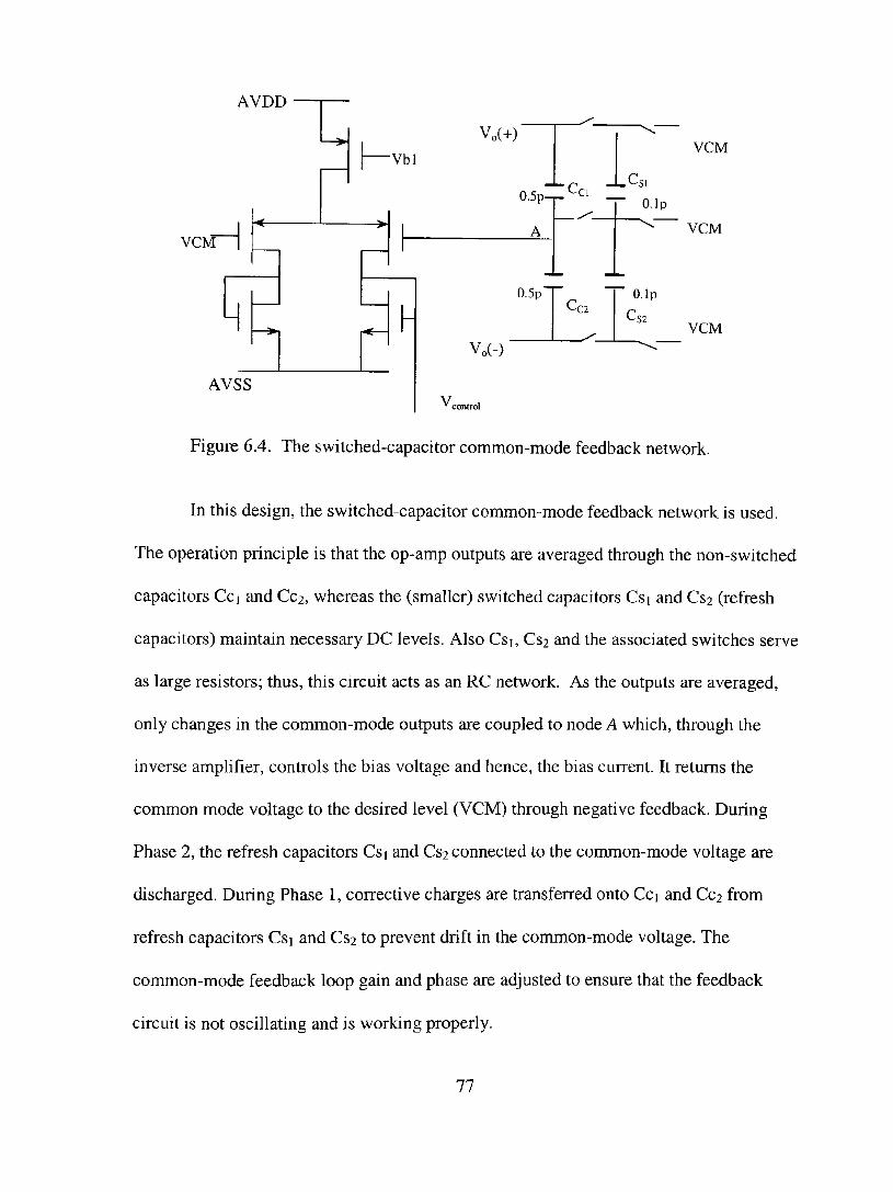
AVDD
VCM
H
AV5 )S
^
-^
-^
"
r<—
Vbl
Vo(+)
Vo(-)
VCM
VCM
VCM
V control
Figure 6.4. The switched-capacitor common-mode feedback network.
In this design, the switched-capacitor common-mode feedback network is used.
The operation principle is that the op-amp outputs are averaged through the non-switched
capacitors Cci and Cc^, whereas the (smaller) switched capacitors Csi and Cs^ (refresh
capacitors) maintain necessary DC levels. Also Csi, Cs^ and the associated switches serve
as large resistors; thus, this circuit acts as an RC network. As the outputs are averaged,
only changes in the common-mode outputs are coupled to node A which, through the
inverse amplifier, controls the bias voltage and hence, the bias current. It retums the
common mode voltage to the desired level (VCM) through negative feedback. During
Phase 2, the refresh capacitors Csi and Cs^connected to the common-mode voltage are
discharged. During Phase 1, corrective charges are transferred onto Cci and Cc^ from
refresh capacitors Csi and Cs^ to prevent drift in the common-mode voltage. The
common-mode feedback loop gain and phase are adjusted to ensure that the feedback
circuit is not oscillating and is working properly.
77

6.2.3 Bias circuit design
The bias circuits provide the bias voltage to the op-amp core to set up the bias
current. Figure 6.5 shows the schematic of the bias circuit. The extemal current reference
/re/and current mirrors are used to generate desired bias voltages Vbi, Vb2, Vb3, and Vb4.
By carefully selecting the aspect ratio WL for different transistors, we can determine the
quiescent bias current A * /;- /for each transistor, where N is the ratio of the transistor
dimension (aspect ratio) to that of the reference transistor.
VDD
MBl r4-
MB2 MB3 r4-
'rer Q MB5
MB6
MB4
VSS
MB7 MBll
3 MB8
3-MB9 MB12
— f 5 MBIO MB13
fr
V,w
Figure 6.5. Bias circuit employing extemal current reference.
In the design of a bias circuit, the transistor of the current mirror is not of the
minimum channel length because of the consideration of the output impedance. To
improved the output impedance, the transistor channel length is made greater than the
78

minimum feature size. The other way to improve the output impedance is to use a
cascode structure to build current mirrors.
6.2.4 Simulation results
The output swing, gain, bandwidth, phase margin and settling time of the
designed op-amp are simulated in Spice. The intrinsic noise of the op-amp is also
simulated and included in the noise budget of the entire system.
a. Output swing: A DC sweep is simulated to check the output swing of the op-
amp. The simulated results show that the linear output swing is about 2.4V.
b. Gain, bandwidth andphase margin: In general, when a DC bias point deviates
from the quasi point which is the bias point of a zero differential output, the DC gain will
decrease due to the change of the saturation condition in the transistors. It is necessary to
check DC gain, bandwidth and phase at different DC output levels. The simulation
results for capacitive load of 6pf in Figure 6.6 show that DC gain decreases by 5dB if the
DC differential output range increases from 0 to 2V. The bandwidth and phase margin,
however, does not vary with the differential output level.
c. Settling time: linear settling time is determined by the bandwidth and phase
margin; the optimum settling occurs at phase margin of ^O '- O^ [44]. The transistor sizes
and the compensation capacitors are carefully designed for fast settling. The key
information conceming the designed op-amp is summarized in Table 6.2.
79
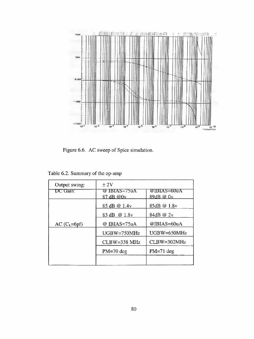
Figure 6.6. AC sweep of Spice simulation.
Table 6.2. Summary of the op-amp
Output swing:
UC (Jain:
AC (CL=6pf)
±2V
(a) IBIAS=75uA 87 dR &0v
85 dB @ I.4v
83 dB @ 1.8v
@ IBIAS=75uA
UGBW=750MHz
CLBW=338 MHz
PM=70 deg
@lBIAi)=60uA 89dR @ Ov
85dB @ I.8v
84dB @ 2v
@IBIAS=60uA
UGBW=650MHz
CLBW=302MHz
PM=7I deg
80
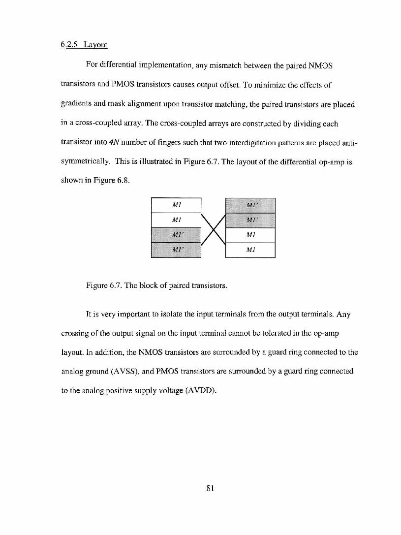
6.2.5 Lavout
For differential implementation, any mismatch between the paired NMOS
transistors and PMOS transistors causes output offset. To minimize the effects of
gradients and mask alignment upon transistor matching, the paired transistors are placed
in a cross-coupled array. The cross-coupled arrays are constructed by dividing each
transistor into 4N number of fingers such that two interdigitation pattems are placed anti-
symmetrically. This is illustrated in Figure 6.7. The layout of the differential op-amp is
shown in Figure 6.8.
Mî
Ml
MP
Mî
Ml
Ml
Ml
Ml
Figure 6.7. The block of paired transistors.
It is very important to isolate the input terminals from the output terminals. Any
crossing of the output signal on the input terminal cannot be tolerated in the op-amp
layout. In addition, the NMOS transistors are surrounded by a guard ring connected to the
analog ground (AVSS), and PMOS transistors are surrounded by a guard ring connected
to the analog positive supply voltage (AVDD).
81
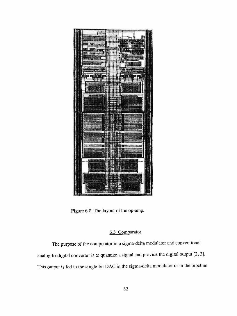
Figure 6.8. The layout of the op-amp.
6.3 Comparator
The purpose of the comparator in a sigma-deha modulator and conventional
analog-to-digital converter is to quantize a signal and provide the digital output [2, 3].
This output is fed to the single-bit DAC in the sigma-delta modulator or in the pipehne
82
converter. The DAC reconverts the digital signal to an analog signal and closes the loop
in the sigma-delta modulator while it converts the digital code to an analog signal to
obtain residue used in the next stage in the pipeline converter.
Three errors, offset, metastability and hysteresis, must be considered in the
comparator design. Offset due to the mismatch of the transistors is the primary concem
for comparator design. Metastability caused by very small input signals is not a problem
if the decision output is latched so that the decision level delivered to the feedback DAC
and that of the digital encoder are the same. Hysteresis due to the nonlinear memory
effects will cause decisions to be dependent on previous decisions. This memory effect
can create unwanted system poles that may cause errors in the signal and noise transfer
functions. The performance of the modulator is relatively insensitive to the offset and
hysteresis because the effects of these impairments are attenuated in the baseband by
second order noise shaping [3]. However, offset and hysteresis will cause nonlinear
errors in the pipeline converter that in tum affect the overall resolution of the converter.
Having considered the above issues, the dynamic latch with preamplifier instead of static
comparator is used as a comparator since only periodic decisions are required. The
differential input is amplified by a gain of about 20dB. The main advantage of using a
preamplifier is to increase the sensitivity that, in tum, reduces the effect of offset.
Another advantage is that the cancellation scheme can be ultilized to cancel the offset.
AIso, the kickback noise due to the dynamic latch is buffered by the preamplifier such
that it does not affect the signal in the previous stages.
83
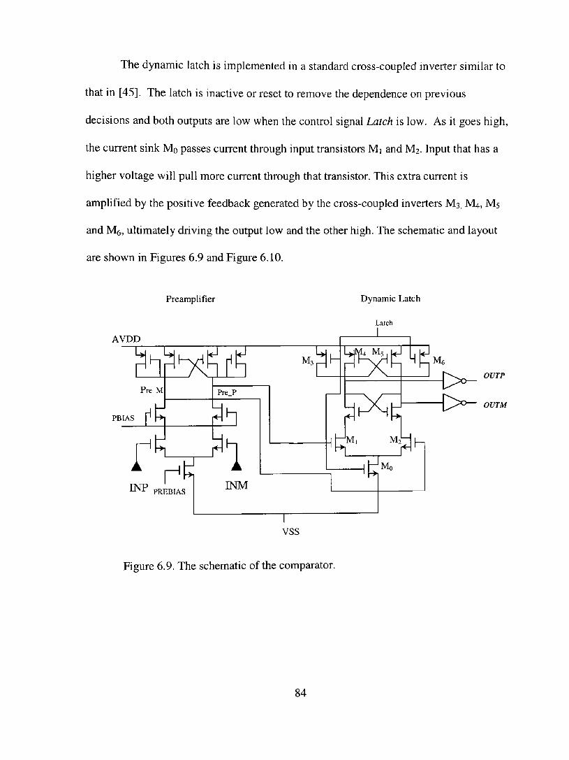
The dynamic latch is implemented in a standard cross-coupled inverter similar to
that in [45]. The latch is inactive or reset to remove the dependence on previous
decisions and both outputs are low when the control signal Latch is low. As it goes high,
the current sink MQ passes current through input transistors Mi and M . Input that has a
higher voltage will pull more current through that transistor. This extra current is
amplified by the positive feedback generated by the cross-coupled inverters M3, M4, M5
and Mô, ultimately driving the output low and the other high. The schematic and layout
are shown in Figures 6.9 and Figure 6.10.
Preamplifier Dynamic Latch
Latch
AVDD
PBIAS
OUTP
OUTM
vss
Figure 6.9. The schematic of the comparator.
84
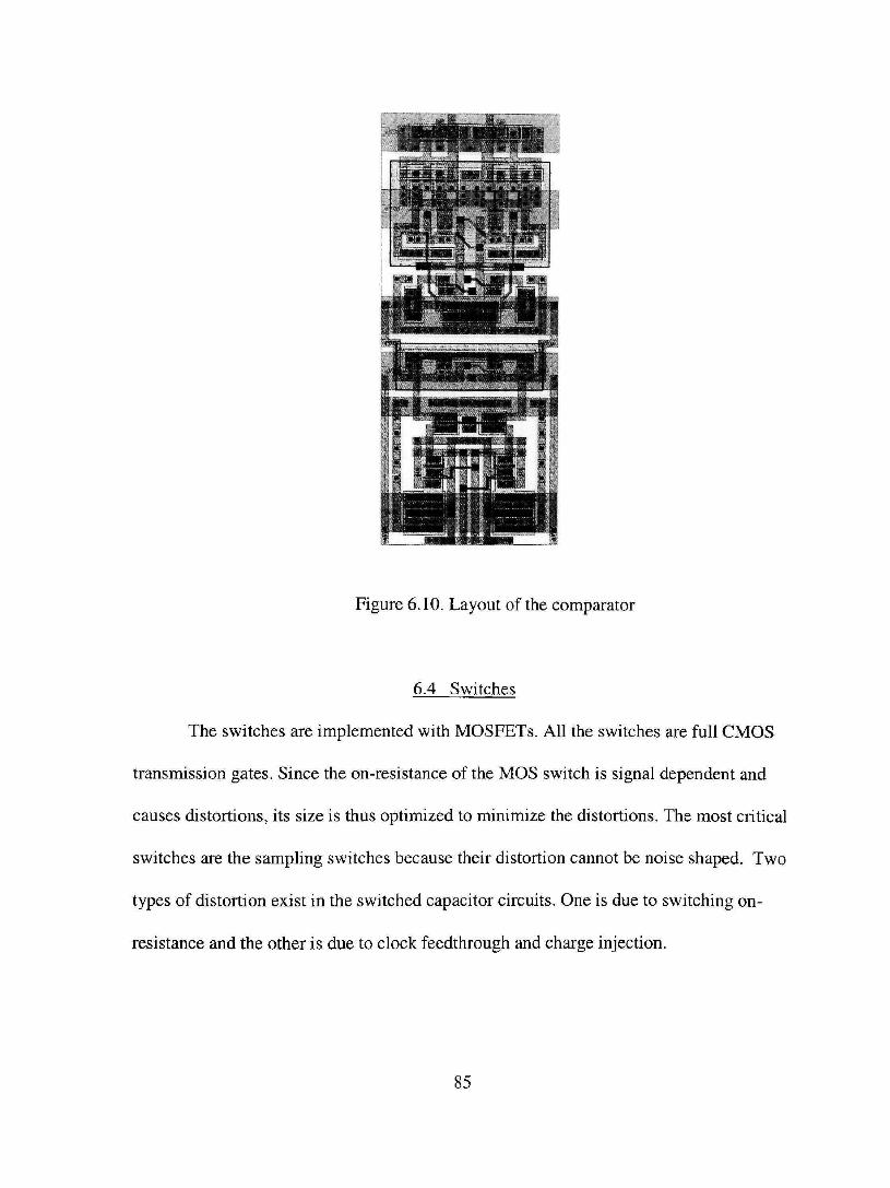
T'-z '- .-,V-f!- 'J
iE if^ssa&^ s,i
^ B P H I Í rMiii • ? •
• . # • . ; - • • ; : ; : a . t
^^^^^HB -ÍS
Figure 6.10. Layout of the comparator
6.4 Switches
The switches are implemented with MOSFETs. AII the switches are full CMOS
transmission gates. Since the on-resistance of the MOS switch is signal dependent and
causes distortions, its size is thus optimized to minimize the distortions. The most critical
switches are the sampling switches because their distortion cannot be noise shaped. Two
types of distortion exist in the switched capacitor circuits. One is due to switching on-
resistance and the other is due to clock feedthrough and charge injection.
85

6.4.1 Signal dependent on-resistance
A typical implementation of sampling capacitor and switches is shown in
Figure 6.11. The switches are implemented by MOSFETs.
^ Vi
SWl
^
SW2
(a) V Vi •c:x=>
Ri+AR
(b) î R2
Figure 6.11. Diagram of the sampling capacitor and switches and the equivalent circuit.
Since the switches are MOSFETs, SWl on-resistance is signal dependent and
time variant [3]. The on-resistance of SW2 is signal independent because its source is
connected to a common-mode voltage that is a DC voltage. The on-resistance of SWl is
R]-\-AR(t) where AR(t) represents the signal dependent portion. It is assumed that
AR(t)«R]+R2=Ro- The voltage across capacitor C for a sinusoidal input Vi=Asin{aX) is
given by
Vc (O -7i + {coRc y
{co - cûRC ) ' sm xcoî - co (6.22)
where RC ^ Rr,C -\- ARC , The following equation can be obtained by expanding
Equation (6.22).
86
( 1 ^^ Vc{t)^A\l--;-{a)RCf {sm{úJt-a)RQC)+cos{ú}t-a)R^C)^{a)ARC)). (6.23)
The distortion terms become
í I ^ AVc(0 = V c ( 0 - A l---{coR^c) sin( ú)t - coR.C) (6.24)
V 2 J
and
AV^(0 = Aû;A7?(OCcos(6î;f-^/?oC). (6.25)
Since the input is a periodic signal, so is AR(t). The magnitude of the distortion is
proportional to the input frequency. The distortion due to sampling switches becomes a
severe problem for wide bandwidth signals in high-speed operation. The distortion-to-
signal ratio (DSR) in dB (assuming that ARmax is the maximum deviation) can be
estimated by the following equation,
DSR = 20 log( coAR^^^ C) - 3 . (6.26)
The following example shows the distortion magnitude for a typical signal input.
Assuming that input frequency/=lMHz, ARmax=\Q., and the sampling capacitor C=4pf,
the distortion-to-signal ratio can be obtained as
D = 201og(2:7r#10^ •l#4*10"^^)-3 = -95dB. However, this value is the total distortion;
the distortion is smaller for fully differential implementation because the even order
harmonics will be cancelled. Moreover, the high-order harmonics outside the baseband
are removed by decimation filters in applications of the sigma-delta modulator.
87
6.4.2 Charge injection
Another type of distortion comes from the clock feedthrough and charge injection.
When the clock signal driving the sampling switches goes low for NMOS and high for
PMOS, the charge stored in the parasitic capacitors and in the channel will be
redistributed as shown in Figure 6.12. It causes nonlinear errors if it is signal dependent.
The effect can be reduced by clock arrangements such that switch SW2 tums off slightly
ahead of switch SWl and by fully differential implementation. As shown in Figure 6.12,
(t)p is identical to ([) except for an advance in the falling edge. SWl provides the path
connection to the low impedance node when SW2 tums off, thus the large part of the
charge is discharged through the low impedance node. The clock feedthrough and charge
injection due to SWI is not important since, when it tums off, the top plate of the
sampling capacitor is floating. The charge injected from SWl, if any, will be stored in
the bottom plate of the capacitors and will be discharged to the common-mode voltage
node (or analog ground) during the next phase. The clock feedthrough and charge
injection due to switch SW2 is signal independent to a first-order approximation since
both the source and drain are always at common-mode voltage when tum-off occurs.
The second effect that may cause distortion is that, even though the total channel charge
of the tum-on switch is signal independent, the manner in which the charge divides when
the switch tums off depends on the impedance on either side of the switch [3]. As
shown in Figure 6.13, if R- is not equal to 7?+, then the charges stored in both sampling
capacitors that are injected from switch SW2 are not equal, i.e., AQ1MQ2. This second
88
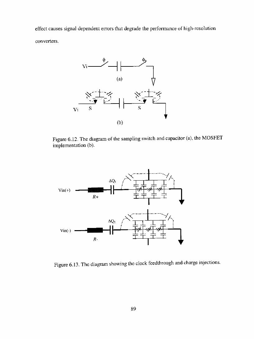
effect causes signal dependent errors that degrade the performance of high-resolution
converters.
Vi > . Øp
(a)
Vi S
V
s
(b)
Figure 6.12. The diagram of the sampling switch and capacitor (a), the MOSFET implementation (b).
Vin(+)
Vin(-)
Figure 6.13. The diagram showing the clock feedthrough and charge injections.
89

The simplest solution to such problems is to reduce AR as much as possible so
that the on-resistance of the switch is flat across the entire input range. The CMOS
transmission gate is one of the choices. The sizes of the NMOS and PMOS need to be
optimized to minimize AR as well as clock feedthrough and charge injection. The more
complicated solution is to keep the gate-source voltage Vgs in on-state (sampling switch,
SWI) input as well as the backgate-source (bulk-source) voltage independent. Therefore,
the on-resistance and the clock feedthrough and charge injection will be signal
independent. They will appear as a DC offset and will be cancelled by differential
implementation. To keep the gate-source voltage and the backgate-source voltage signal
independent, several techniques can be used. For example, the sampling switch can be
bootstrapped such that Vgs is almost constant across entire input level range [3, 24] and
the well of the device is connected to the source.
6.4.3 Simulation results
Since the distortion due to clock feedthrough and charge injection is impossible to
treat analytically, SPICE simulation is used. Both CMOS transmission gate switches and
bootstrapped switches are simulated. Although bootstrapped switches provide less
distortion than that of CMOS transmission gates, the circuits to implement them are much
more complicated. The simulated results for CMOS transmission gates shown in Figure
6.14 also satisfy the requirement in this design. Only the odd harmonics are apparent; the
even order harmonics are cancelled by fully differential implementation. The maximum
distortion is a third harmonic which islOSdB below the peak signal at the input frequency
90
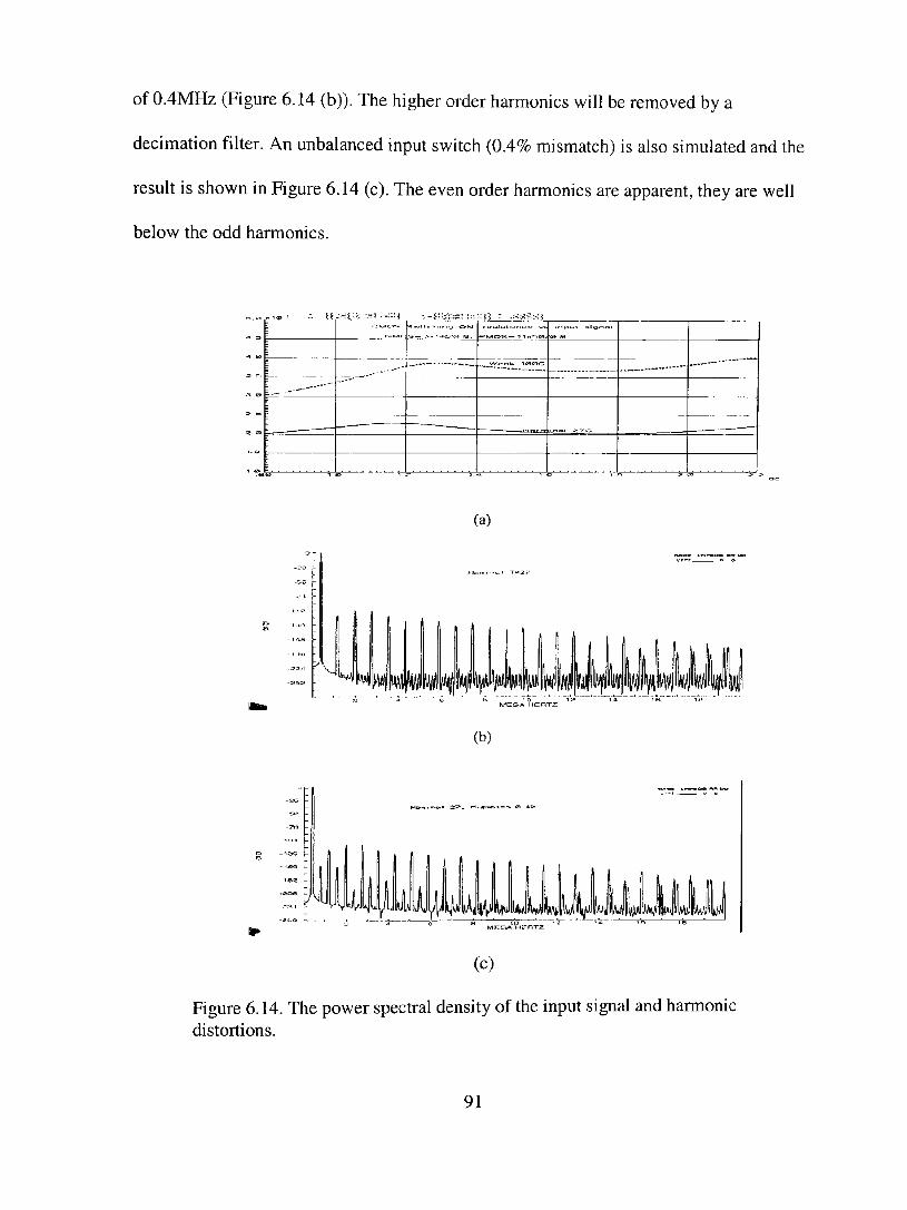
of 0.4MHz (Figure 6.14 (b)). The higher order harmonics will be removed by a
decimation filter. An unbalanced input switch (0.4% mismatch) is also simulated and the
result is shown in Figure 6.14 (c). The even order harmonics are apparent, they are well
below the odd harmonics.
t '"* ' - ít
1
[ . — - • " " "
Tm-n
r
\ — •
i
i
; - í í - : ;
,:^--—
- : : : Í - - , - Í : : ; ; ; ! : - ; I i t : : i 3 : -rWiîF^rií
^ — •' -• ' ^ " ^
~
- . „„=„ . . . - . . . -< . _ . , . . _ v - . . . ^^ = .
- —^r.:^t,.l^*^'^ —
l í - io l y;>-cr
-
VI '+vMy|iiiiyifi^
(a)
(b)
w m rvEí jA ittznrrz:
I I ] i f
'jyifMiyMU) Mi
o --13«;
MKOA n F r t x z
(c)
Figure 6.14. The power spectral density of the input signal and harmonic distortions.
91

6.5 Second-order modulator
There are two types of switched capacitor implementation of second-order
modulators. One is based on Candy's structure in which the first integrator does not have
a unit delay while the second integrator is implemented with a unit delay. The overall
loop delay is one unit. The other version is implemented by Wooley et al. [21] and has
one unit delay in each of the two integrators. Mathematically, both give the same output
and the same noise shaping, but extensive SPICE simulation results reveal that the former
requires less output swing for the same input signal. The lesser output swing requirement
is a big advantage for low-voltage applications. Therefore, the second-order modulator
implemented in this design is based on Candy's stmcture. Figure 6.15 shows its fuUy
differential, switched capacitor CMOS implementation. It consists of two parasitic-
insensitive integrators, a comparator, and a one-bit DAC. The comparator serves as the
one-bit quantizer. The one-bit DAC is implemented such that the positive reference
voltage or the negative reference voltage will be chosen as the output based on the level
of the modulator's output bit. For example, if the output bit is 1, then the positive
reference voltage is chosen; otherwise, the negative reference voUage is chosen. The
modulator operates on a two-phase, non-overlapping clock phase.
For the first integrator, in Phase (t)2, all of the switches at the input switch are
tumed on, connecting the bottom plate of the samphng capacitor Ci to input signals Vi""
and Vi". The top plates are connected to the common mode voltage VCM. In Phase (t)l,
the top plates of the sampling switches are connected to a 1-bit DAC and the bottom
plates are connected to the inverse input of the op-amp. The 1-bit DAC is implemented
92

by connecting to the positive reference or negative reference vohage, depending on the
output of the comparator; thus, it is inherently linear. The charges are integrated into
integrating capacitors C2 and C2'. For the second integrator, in Phase 4)1, all of the
switches at the input of A2 are tumed on, connecting the bottom plate of the sampling
capacitor Ci to the output of the first integrator. The top plates are connected to the
common mode voltage VCM. The bottom plates of C3 and C3' are connected to the 1-bit
DAC and the top plates are connected to the inverse input of the op-amp that gives the
output quantization error of the second order modulator entering the next stage. In Phase
([)2, the bottom plates of the sampling switches are connected to common mode voltage
VCM, and the top plates are connected to the inverse input of the op-amp. The charges
stored in capacitors C2 and C2' are integrated by integrating capacitors C f and C f'. Both
top plates and bottom plates of the capacitors C3 and C3' are connected to the common
mode voltage VCM. The output of the second integrator enters the comparator in the
same phase. The Latch signal goes active and the decision is made right after the falling
of phase (t)2. The output of the quantizer is valid during the next phase, (\>\. Therefore, the
overall loop delay is one clock cycle. The delayed versions of clock phases, (j)ld and (t)2d,
are used to minimize the signal dependent charge injections of the sampling switches as
discussed in section 6.4.2.
The ratio of the capacitance of the samphng capacitor to that of the integrating
capacitor determines the gain of the integrator (see Appendix A). The ratios C^ I C j and
C2 / Cj^ are set to be 0.5, and the ratio of C^ I Cj^ is set to be 0.25 to increase the input
93
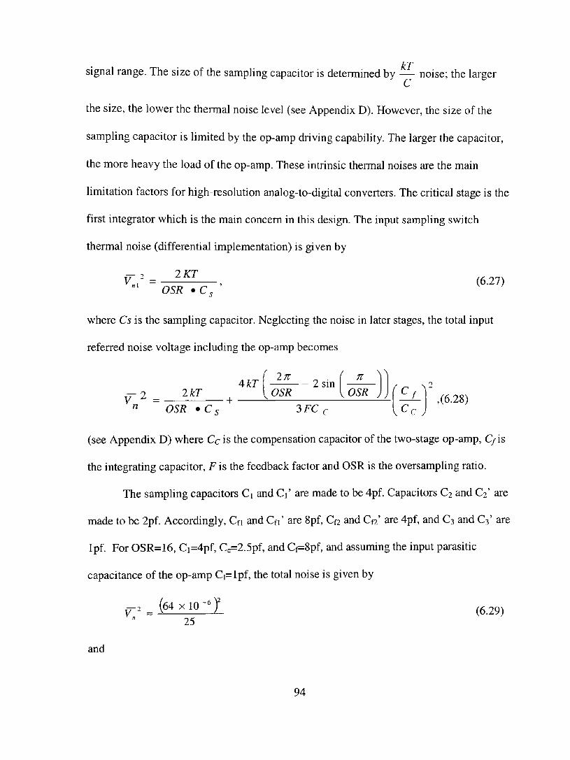
signal range. The size of the sampling capacitor is determined by — noise; the larger
the size, the lower the thermal noise level (see Appendix D). However, the size of the
sampling capacitor is limited by the op-amp driving capability. The larger the capacitor,
the more heavy the load of the op-amp. These intrinsic thermal noises are the main
limitation factors for high-resolution analog-to-digital converters. The critical stage is the
first integrator which is the main concem in this design. The input sampling switch
thermal noise (differential implementation) is given by
V-J = ^^^ , (6.27) "' OSR • C ,
where Cs is the sampling capacitor. Neglecting the noise in later stages, the total input
referred noise voltage including the op-amp becomes
T-^2 2Â:r V = +
4kT ' In f ^ \^
OSR - 2 sin n
OSR r r^ \^-C f K^C J
,(6.28) " OSR • C 5 3FC c
(see Appendix D) where Cc is the compensation capacitor of the two-stage op-amp, C/is
the integrating capacitor, F is the feedback factor and OSR is the oversamphng ratio.
The sampUng capacitors Ci and Ci' are made to be 4pf. Capacitors C2 and C2' are
made to be 2pf. Accordingly, Cfi and Cfi' are 8pf, Cf2 and Cf ' are 4pf, and C3 and C3' are
Ipf. For OSR=16, Ci=4pf, Cc=2.5pf, and Cf=8pf, and assuming the input parasitic
capacitance of the op-amp Ci=lpf, the total noise is given by
- , __ ( 6 4 x 1 0 - 0 ^ (6.29) 25
and
94
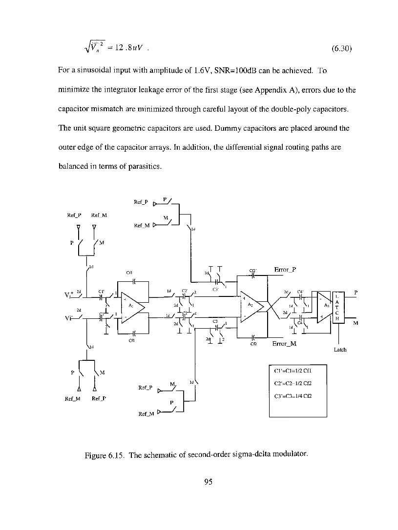
^lvJ=\2.SuV (6.30)
For a sinusoidal input with amplitude of 1.6V, SNR=100dB can be achieved. To
minimize the integrator leakage error of the first stage (see Appendix A), errors due to the
capacitor mismatch are minimized through careful layout of the double-poly capacitors.
The unit square geometric capacitors are used. Dummy capacitors are placed around the
outer edge of the capacitor arrays. In addition, the differential signal routing paths are
balanced in terms of parasitics.
Ref p
Ref P Ref M
Ref M Ref P
Ref M
Cl'=Cl=l/2Cfl
C2'=C2=l/2 Cf2
C3'=C3=l/4Cf2
Latch
Figure 6.15. The schematic of second-order sigma-delta modulator.
95

6.6 Pipehne ADC
The 8-bit quantizer following the second-order sigma-deha modulator is
implemented using a pipelined structure. There are many types of pipelined architectures.
Some use one bit per stage, some use multi-bits per stage, and others use a mixture of
both.
The 8-bit pipeline ADC is implemented as 1.5-bit resolution per stage with
redundancy signed digit (RSD). The major advantage is that the offsets due to the
comparator, op-amp, charge injection and capacitor mismatches can be digitally
corrected. In this design, a total offset up to V4 reference voltage can be tolerated [see
Appendix B]. The schematic is shown in Figure 6.16. In Phase ^2, the reference voltages
are charged to Ci, Ci', C2, and C2', and the comparator offset is also stored in the same
capacitors. In Phase (t)l, the input signal (either the output of the second-order modulator
or the previous stage's residual output) is entered and the decision is made right after the
signal is settled to the final value.
The residual output is obtained by a muItiply-by-2 block (inside the dotted line).
During the sampling Phase (t)l, the input signal is sampled to capacitors Cs and Cf
(Cs=Cf). The offset due to the op-amp is stored to capacitors Cs and Cf in the same phase.
In amphfication Phase (t)2, the capacitor Cf is swapped to be the feedback capacitor. Its
bottom plate is connected to the output terminal of the op-amp and the top plate is
connected to the inverse input terminal of the op-amp. The bottom plates of the capacitor
Cs are connected to the MDAC output that is either a positive reference vokage, a
96

negative reference voltage, or a common-mode voltage, depending on the decision made.
Thus, the residual output is obtained such that
V^=2V^-dy^^^. (6.31)
where V, is the residual output entering into the next stage, and V/ is the input signal
entering this stage. Vr^/is the reference voltage, anddiis the decision that has been made,
whichcanbeei ther-1, +1 orO.
The 8-bit pipelined quantizer consists of 8 such identical stages. The residual
output of the last stage enters the first-order single-bit sigma-delta modulator to be
discussed in the next section.
The capacitors Cs and Cf are made to be Ipf. They are not scaled down as they
should be in the later stages simply because of the simplicity of implementation. Each
stage is laid out symmetrically; the differential signals' routing paths are carefully
balanced to minimize the mismatches. AII signal paths are shielded from clock signals
and any other signals by metal layers connecting to the analog ground. They are placed
side by side horizontally to reduce the complexity of routing.
97

Vi_P
Vi_M
REF1_P j o / .
2áy
REFl M
Id
REF2_P _2^_
\\ \ Id
^ "
\ "
Id
Id
J/.
^ y\
y\
*ES_P
£ES_M
'-^. REF
3_
3"— S 2 /
—^ VCM
X — ~ REF_P ^
S3^. S3
REF_P
VCM
M
^ . .
\ s, h
1/. Latch
REF2 M
X
H>H> Dl '^ D l
O — Sl
o^>J^ DO' DO
o— S2
S3
M
Latch
Dl DO Sl
0 0 0
0 I 0
1 0 1
S2
0
1
0
S3
1
0
0
Vin<REF2
REF2<Vin<REFl
Vin>REFl
Figure 6.16. The schematic of one stage of the pipeline ADC.
6.7 First-order modulator
Figure 6.17 shows a fully differential, switched capacitor CMOS implementation
of the first-order sigma-delta modulator. It consists of a parasitic-insensitive integrator, a
comparator that serves as the one-bit quantizer, and a distributed one-bit DAC. The
98

modulator operates on two-phase non-overiapping clock phases. In Phase (t)l, all of the
switches in the input switch are tumed on, connecting the bottom plate of the sampling
capacitors Ci to input signals Vi'' and Vi". In the same phase, the bottom plates of C2 and
C2' are connected to a one-bit DAC output which is either a positive reference voltage or
a negative reference voltage. The top plates of Ci are Ci'are connected to common mode
voltage VCM, and those of C2 and C2' are connected to the input terminals of the op-
amp. This causes a transfer of charge from sampling capacitor C2 onto the integrating
capacitor Cf; thus, quantization errors, ERROR_P and ERROR_M, which are the inputs
of the flash ADC, are obtained by subtracting the DAC outputs from the integrator output
of the previous Phase ^2. In Phase (t)2, the bottom plates of the sampling capacitors Ci
and Ci'are connected to the common-mode voltage, and the top plates are connected to
the input terminals of the op-amp. This causes a transfer of charge from the sampling
capacitor to the integration capacitor. The integrator output is sampled by capacitors C3
and C3' in Phase (^2. The charges on C2 and C2' are discharged by connecting both the
bottom and top plates to the common mode voltage. By the end of Phase (t)2, the Latch
signal goes active, thus causing ''decision making." As stated previously, the offset
cancellation scheme is used. In Phase (|)1, the bottom plates of capacitors C3 and C3' are
connected to the common-mode voltage and the top plates are connected to the input
terminals as well as the output terminals of the preamplifier; thus, the offsets are stored in
C3 and C3'. Therefore, the offsets do not affect the decision making in the next phase.
99
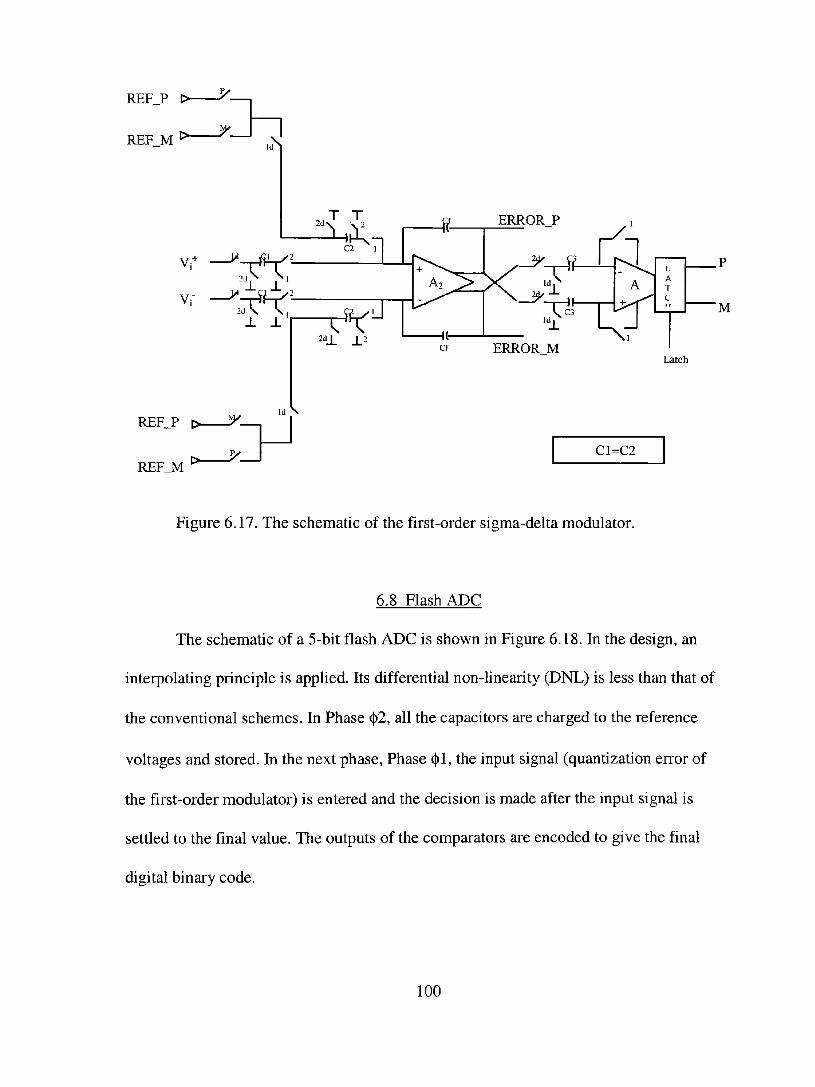
REF P >
REF M ^
Vi^
vr
5^_|J
2d
REF_P t> ^ I
REF M ^
Id N
T T
1.Í C2 :3
í^ 2dJ_ _L2
a
fí-
A.2
Cf
ERROR P
i : í
î C3
ERROR M
A
C1=C2
Latch
M
Figure 6.17. The schematic of the first-order sigma-delta modulator.
6.8 Flash ADC
The schematic of a 5-bit flash ADC is shown in Figure 6.18. In the design, an
interpolating principle is applied. Its differential non-linearity (DNL) is less than that of
the conventional schemes. In Phase (t)2, all the capacitors are charged to the reference
voltages and stored. In the next phase, Phase (t)l, the input signal (quantization error of
the first-order modulator) is entered and the decision is made after the input signal is
settled to the final value. The outputs of the comparators are encoded to give the final
digital binary code.
100
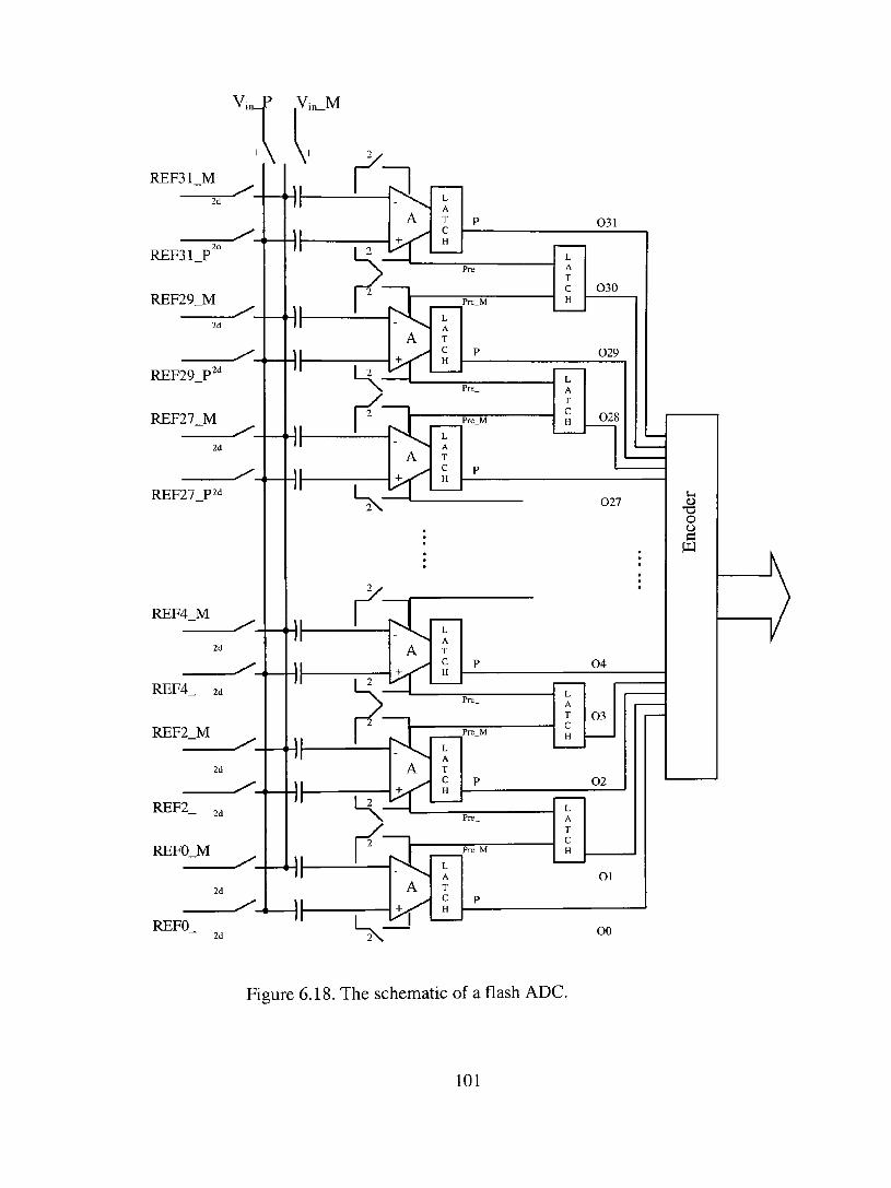
V. Vi.. M
REF31 M
2d
REF31_P
REF29 M
2d
REF29_P
REF27 M
2d
REF27 P-
REF4 M
2d
REF4_ 2d
REF2 M
REF2 2d
REFO M
2d
REFO 2d
\ \ '
Figure 6.18. The schematic of a flash ADC.
101

6.9 Clock generator
6.9.1 Nonoverlapped two-phase clock generator
To make the switched capacitor circuits operate properiy, the clocks driving the
switches must be designed accordingly. The timing to tum the switches on or off is very
important in switched capacitor circuits. A schematic of a two-phase nonoverlapping
clock generator similar to that in [46] is shown in Figure 6.19. This circuit is used in most
switched capacitor circuits. It generates clock phases PHPl and PHP2, and the inverted
forms, PHIPZ and PH2PZ, in order to drive both NMOS and PMOS switches. The
delayed versions of clock phases, PHl, PH2, PHIZ, and PH2Z are also generated.
Traditionally, both rising and falling edges of the clock are delayed in order to generate
the delayed waveforms [38]. In fact, to avoid signal-dependent charge injection, only the
falhng clock edge needs to be delayed. Hence, in this design the falling edges are delayed
and the rising edges are synchronized to efficiently use the short period. The clocks
generated are further buffered to drive the switches.
6.9.2 Clock jitter effect
Clock jitter is another source that degrades the overall performance of a system
implemented in switched capacitor circuits. If the clock's period is not constant (due to
the generator and interference from the substrate), the signal is sampled in a non-uniform
clock cycle which causes distortion. Thus, the signal to noise plus distortion ratio
decreases.
102
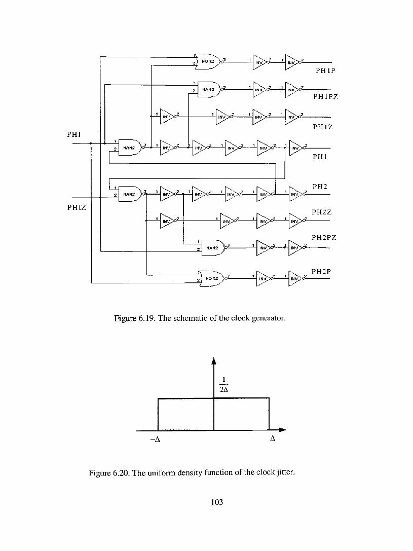
PHI
PHIZ
> .
3 1
PHIP
2 NAM2 yc3-
NAN2
PHIPZ
2 1
PHIZ
PHl
PH2
PH2Z
PH2PZ
PH2P
Figure 6.19. The schematic of the clock generator.
_\_ 2A
-A
Figure 6.20. The uniform density function of the clock jitter.
103

The effect of the clock jitter can be derived by assuming that the sampling period
at the i ^ clock Ti = To+ATi, where TQ is the desired clock period and ATi is a random
variance with uniform distribution (the more realistic assumption might be normal
distribution) shown in Figure 6.20. For a sinusoidal input, we have the sampled discrete
signal,
V inT ) = A sin( coI.T^) = A sin( COITQ + coI.A T^) . (6.32)
Assuming that the second term inside the parenthesis of Equation 6.32 is very small, then
Equation 6.32 can be rewritten as the following:
V{nT)= A sin( ænT^) + A cos( CúnTQ ){ú)I.A T.) . (6.33)
The first term is the desired discrete signal without clock jitter, and the second term is the
distortion caused by the clock jitter. Assuming that clock jitter is white noise, the signal-
to-distortion ratio (SDR) is given by
SDR=\0\og^^^ = \0\og{OSR)-20\og{ûA)-^5dB (6 34)
arâi
For the requirement of SDR=100dB and the signal frequency of/=lMHz, A=10ps is
tolerated for oversampling ratio OSR=16.
6.10 Svstem integration and layout issues
The subsystems described above are integrated to form the entire system shown in
Figure 6.1. The die photo of the entire chip is shown in Figure 7.1. In this design,
extemal off-chip instead of on-chip reference voltages and currents are used. The
differential input enters the chip from the left, and the third and fourth pad from the top.
104

The paths are carefully layed out to balance the impedance from the input pad to the
sampling switches. The analog signal pads are placed on the left and bottom sides and the
digital signal pads are placed on the top and right sides. The routing of digital signals
such as clocks and data outputs are carefully designed to avoid line crossing and coupling
with analog signals, and they are isolated or shielded from analog signals if the line
crossing cannot be avoided. The analog signal paths are shielded from any other signals
by other metal layers connected to a ground.
In mixed-signal design, it is important to minimize the impact of noise coupling
from the digital circuitry to the sensitive analog circuitry via the conmion substrate. The
most effective way to reduce substrate noise is to create a low-impedance path from the
p+ substrate to ground. In this design, the following approaches are taken. Separate
supplies are used for digital (DVDD and DVSS) and analog (AVDD and AVSS) signals.
Because an N-well process is used, the digital and analog PMOS transistors were isolated
by separate wells. The NMOS transistors, however, interact via the common, low-
resistance p+ substrate. The noise travels almost exclusively in the p+ region because of
the low resistance. To prevent substrate noise coupling, each analog and digital block is
surrounded by a grounded guard rings and is also isolated from the others by DUF
connected to a ground, VSS. In the prototype, a separate substrate pin VSS was used to
set the substrate potential. Contacts between VSS and the substrate were made liberally in
the digital areas to provide a low-impedance path to ground for substrate noise. AVSS,
DVSS, and VSS are disjoint on-chip; however, they can be connected together off-chip.
105

The prototype of the chip has 48 pins. The pins in the analog portion are on the
right and bottom sides, and those in the digital portion are on the left and up sides. This
pin arrangement results in easy layout for the PCB design and testing.
106
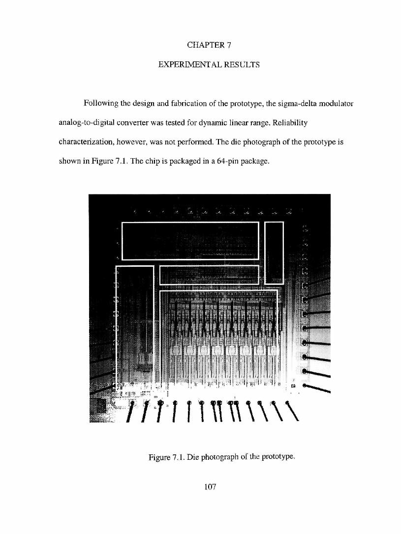
CHAPTER 7
EXPERIMENTAL RESULTS
FoIIowing the design and fabrication of the prototype, the sigma-delta modulator
analog-to-digital converter was tested for dynamic linear range. Reliability
characterization, however, was not performed. The die photograph of the prototype is
shown in Figure 7.1. The chip is packaged in a 64-pin package.
//rnnnuvw Figure 7.1. Die photograph of the prototype.
107
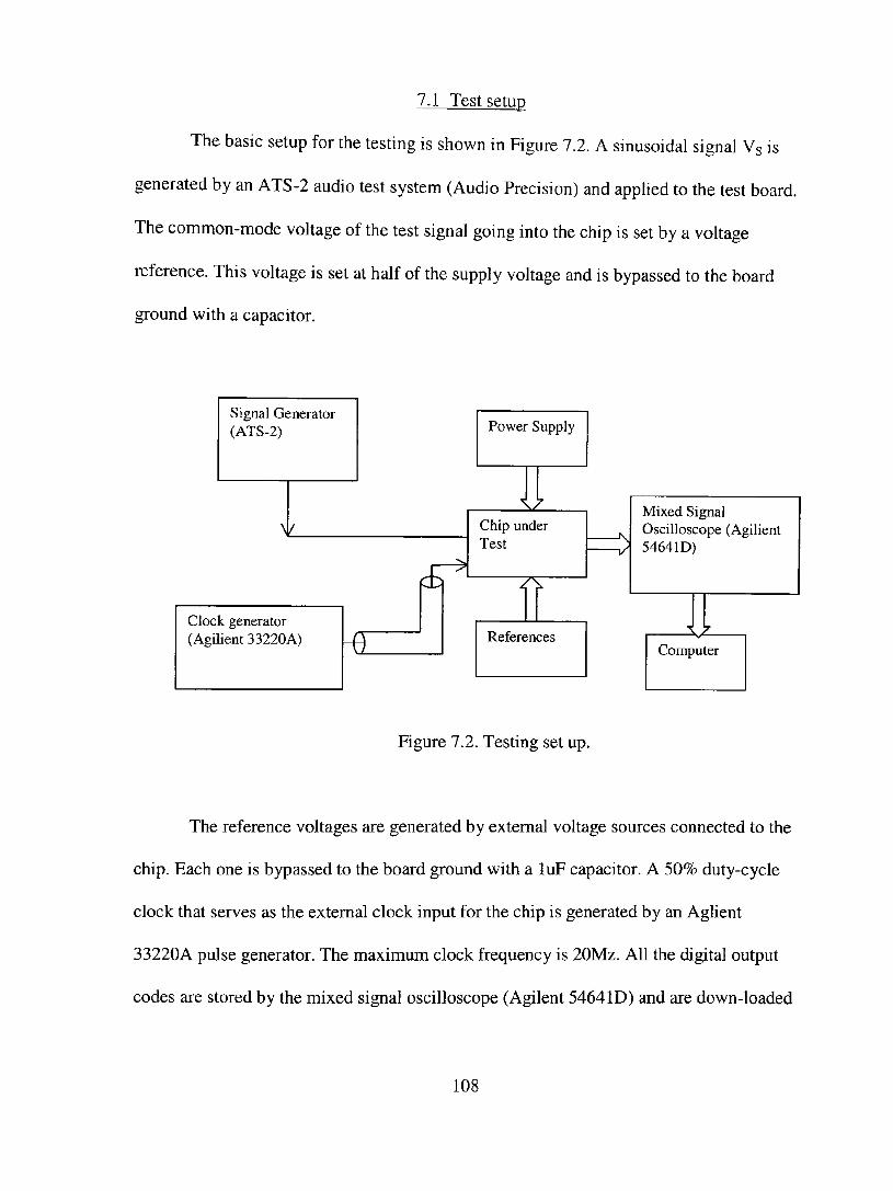
7.1 Test setup
The basic setup for the testing is shown in Figure 7.2. A sinusoidal signal Vs is
generated by an ATS-2 audio test system (Audio Precision) and applied to the test board.
The common-mode voltage of the test signal going into the chip is set by a voltage
reference. This voltage is set at half of the supply voltage and is bypassed to the board
ground with a capacitor.
Signal Generator (ATS-2)
N^
Clock generator (Agilient 33220A) -e
Power Supply
(h ^
Iz Chip under Test
7Y
References
Mixed Signal Oscilloscope (Agilient 54641D)
XZ Computer
Figure 7.2. Testing set up.
The reference voltages are generated by extemal voltage sources connected to the
chip. Each one is bypassed to the board ground with a luF capacitor. A 50% duty-cycle
clock that serves as the extemal clock input for the chip is generated by an Aglient
33220A pulse generator. The maximum clock frequency is 20Mz. AII the digital output
codes are stored by the mixed signal oscilloscope (Agilent 5464ID) and are down-loaded
108

to a computer where the digital cancellation and filtering is done in software. Then the
FFT is performed to obtain the power spectral density, and the signal-to-noise ratio is
calculated.
The power supplies are decoupled to their corresponding ground, as close to the
chip as physically possible; 0.1 iF ceramic capacitors are used. It is worthwhile to point
out that the power supplies and the corresponding ground pins are co-Iocated on the chip
to simplify the layout of the decoupling capacitors and provide the shortest possible PCB
trace length. The supplies for clock driver, digital and output buffers are separate to avoid
modulating the clock signal with digital switching noise. AII supplies are separated from
the analog power supply. The master current to generate the bias current for all analog
circuitry is generated extemally.
A two-layer printed circuit board is used. The chip under test is in a 64-pin socket.
7.2 Dvnamic linear range
The dynamic range and noise performance of the converter can be characterized
by a signal-to-noise-plus distortion ratio (SNDR) measurement. The SNDR is defined as
the ratio of the signal power to all other noise and harmonic power in the digital output
stream. The dynamic range is defined as the difference between the largest signal and the
smallest signal (in dB) that can be detected in the presence of noise. The peak SNDR is
the highest achievable SNDR for a given converter. In the testing, for the sake of the
available facility, the clock frequency is set to be 20MHz (designed for 40MHz) and the
signal frequency is 50kHz. Figure 7.3 shows the typical power spectral density of the
109
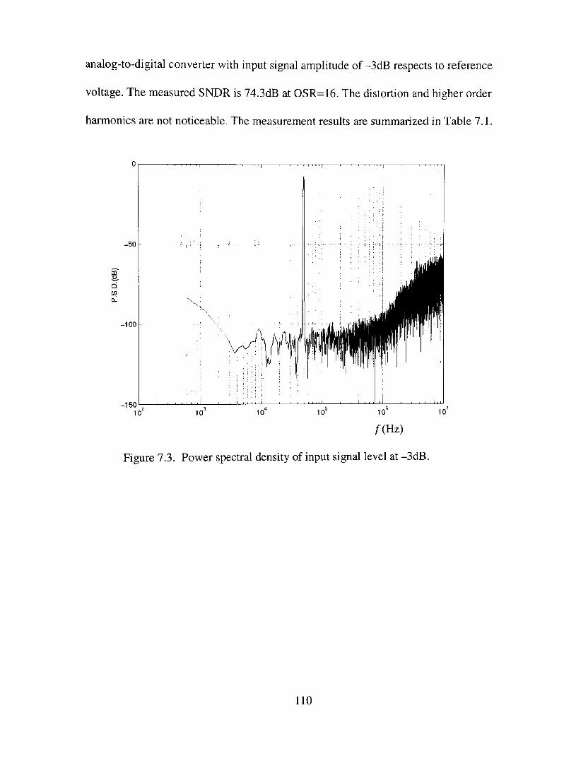
analog-to-digital converter with input signal amplitude of-3dB respects to reference
voltage. The measured SNDR is 74.3dB at 0SR=16. The distortion and higher order
harmonics are not noticeable. The measurement results are summarized in Table 7.1.
•100
-150
/•(Hz)
Figure 7.3. Power spectral density of input signal level at -3dB.
110
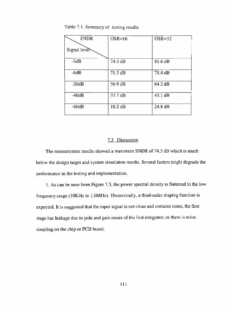
Table 7.1. Summary of testing results
^ ^ SNDR
Signal level^^
-3dB
-6dB
-20dB
-40dB
-60dB
0SR=16
74.3 dB
71.5 dB
56.9 dB
37.7 dB
18.2 dB
OSR=32
81.6 dB
78.4 dB
64.2 dB
45.1 dB
24.8 dB
7.3 Discussion
The measurement results showed a maximum SNDR of 74.3 dB which is much
below the design target and system simulation results. Several factors might degrade the
performance in the testing and implementation.
1. As can be seen from Figure 7.3, the power spectral density is flattened in the low
frequency range (lOKHz to l.OMHz). Theoretically, a third-order shaping function is
expected. It is suggested that the input signal is not clean and contains noise, the first
stage has leakage due to pole and gain errors of the first integrator, or there is noise
coupling on the chip or PCB board.
111
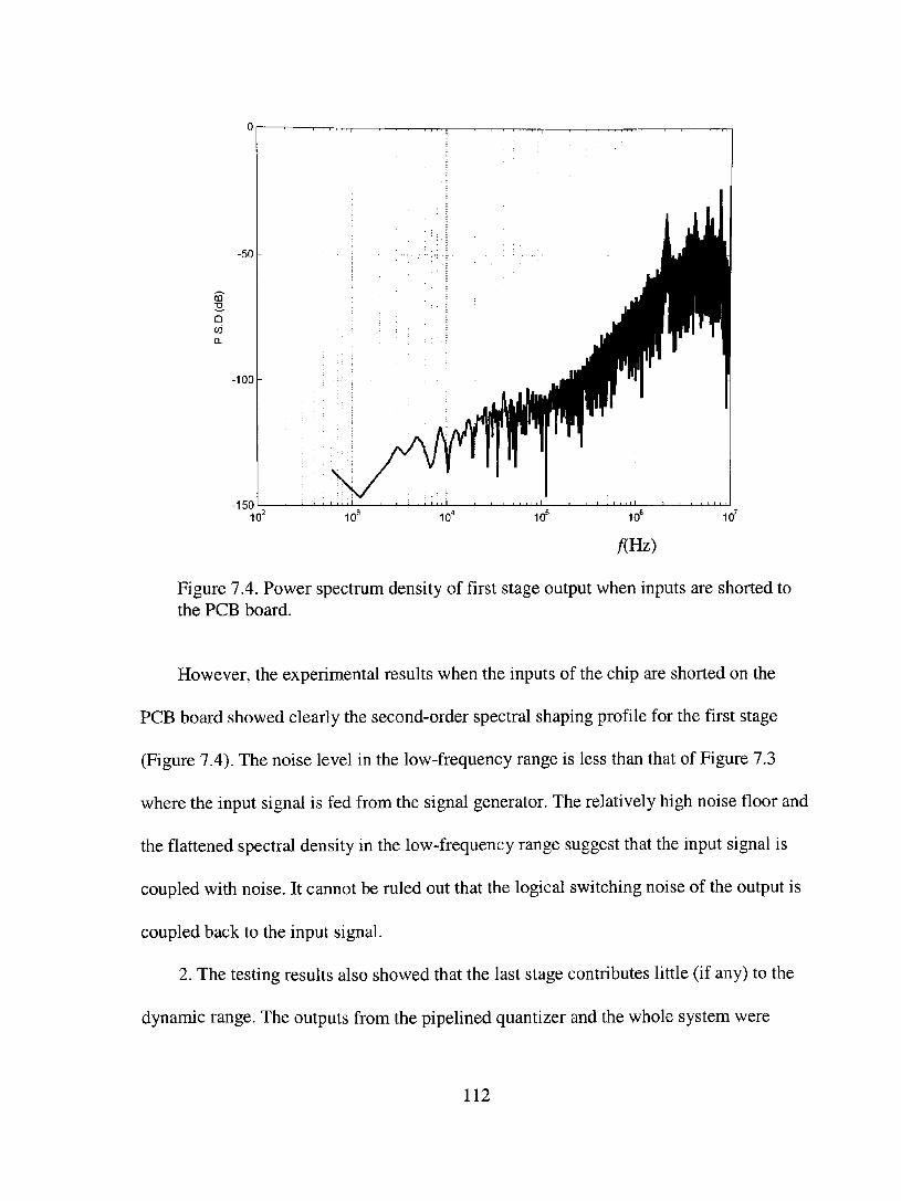
-100
•150
m Figure 7.4. Power spectrum density of first stage output when inputs are shorted to the PCB board.
However, the experimental results when the inputs of the chip are shorted on the
PCB board showed clearly the second-order spectral shaping profile for the first stage
(Figure 7.4). The noise level in the low-frequency range is less than that of Figure 7.3
where the input signal is fed from the signal generator. The relatively high noise floor and
the flattened spectral density in the low-frequency range suggest that the input signal is
coupled with noise. It cannot be mled out that the logical switching noise of the output is
coupled back to the input signal.
2. The testing results also showed that the last stage contributes little (if any) to the
dynamic range. The outputs from the pipelined quantizer and the whole system were
112

compared; the results suggested that the last stage (first-order modulator with 5-bit flash
ADC) contributed little to the SNDR improvement. This also suggested that the pipelined
quantizer, has less resolution and the integrating linearity is not as good as designed.
Usually, op-amp gain, comparator offset, the clock timing mismatch and reference
voltage noise are the main sources for limiting the resolution and integrating linearity.
The designed op-amp gain is very high so that it exceeds the requirement used in the
system-level simulation, and it is the same as used in the first stage. The comparator
offsets has been carefully taken care of by the design and the layout. A redundant bit is
also used to minimize the effect of the comparator offset.
The clock timing skew and mismatching due to parasitics are also limiting factors
for the pipeline quantizer, especially when the sampling clock falling edge comes just
after the comparator latch's rising edge. The sampled signal will be contaminated by the
switching noise. A good timing scheme is that the comparator latch happens just after the
sampling clock falling edge. This involves timing adjustment with delay lines and
parasitic extraction simulation that was lacking in the layout phase.
113

CHAPTER 8
CONCLUSIONS
A multi-stage muhi-bit sigma-delta modulator with interstage gain scaling has
been designed and implemented in a 0.6 |im CMOS process. It employs a second-order
single-bit modulator in the main stage followed by an 8-bit quantizer (pipeline structure).
The second-stage consists of a first-order single-bit modulator followed by a 5-bit
quantizer. Gain is applied between those two stages to scale the signal level to the
reference level. System and circuit level simulations show that it achieves high speed and
high resolution. The detailed design considerations in CMOS implementation have also
been analyzed and discussed. The prototype has been fabricated in a 0.6 |i,m CMOS
process with 3.3V power supply. Experiments at testing of the prototype have also been
performed.
It has been demonstrated in the system level simulation that the proposed
modulator has the potential to achieve high speed and high resolution in analog-to-digital
conversion. However, the experimental results of the prototype showed lower
performance than designed for. Several factors and issues hmiting the achievable high
performance are discussed. Further improvements are needed in the implementation.
114
REFERENCES
1. Van De Plassche, R., Integrated analog-to-digital and digital-to-analog converters. Kluwer Academic Publishers, Norwell, MA, 1994.
2. Candy, J. C. and Temes, G. C. (Ed.): Oversampling delta-sigma data converters: theory, design, and simulation. lEEEPress, New York, 1992.
3. Norsworthy, S. R., Schreier, R., and Temes, G. C. (Ed.): Delta-sigma data converters. lEEE Press, New York, 1997.
4. Aziz, P. M., Sorensen, H. V. and Van Der Spiegel, J. "An Overview of sigma-delta converters," lEEE Signal Processing Magazine, pp. 61-84, 1996.
5. Sevenhans, T, and Chang, Z.Y., " A/D and D/A conversion for telecommunication," lEEE Circuits & Devices Magazine, pp. 33-42, 1998.
6. Razavi, B., Principles ofdata conversion system design. lEEE Press, New York, 1995.
7. Culter, C. C , " Transmission systems employing quantization," 1960 U.S. patent No. 2,927,962 (filed 1954).
8. Inose, H., Yasuda,Y., and Murakami,J., "A telemetering system code moduIation-A-2 modulation," IRE Trans.Space Elect. Telemetry, Vol. SET-8, pp. 204-209, 1962.
9. Friedman, V., "Oversampled data conversion techniques: the mix of sigma-delta modulation and DSP produces an explosion in the variety and complexity of a-d and d-a converters implemented in MOS technology," lEEE Circuits & Devices Magazine, pp. 39-46, 1990.
10. Candy, J. C , " A use of double integration in sigma-delta modulation," lEEE Trans. Commun., Vol. COM-33, pp. 269-258, 1985.
11. Uchimura, K., Hayashi, T., Kimura, T., and Iwata, A., "Oversampling a-to-d and d-to-a converters with multistage noise shaping modulators," lEEE Trans. Acoust., SpeecK Signal Processing, Vol. AASP-36, pp. 1899-1905, 1988.
12. Chao, K.C, Nadeem, S., Lee, W. and Sodini, C , "A higher order topology for interpolative modulators for oversampling A/D converters," lEEE Trans. Circuits and Systems, Vol., CAS-37, pp. 309-318, 1990.
115
13. Cataltepe, T., Kramer, A.R., Larson, L.E., Temes, G.C and Walden, R.H., " Digitally corrected multi-bit AE data converters," lEEE Intemational Symposium on Circuíts and Systems, pp. 647-650, 1989.
14. Fattaruso, J.W., Kiriaki, S., de Wit, M., and Warwar, G., "Self-calibration techniques for a second-order multi-bit sigma-delta modulator," lEEE loumal of Solid-State Circuits, Vol. 28, pp. 1216-1223, 1993.
15. Baird, R.T. and Fiez, T.S., " Improved AS DAC linearity using data weighted averaging," 1995 lEEE Inîemational Symposium on Circuits and Systems, pp.13-16, 1995.
16. Baird, R.T. and Fiez, T.S., " Linearity enhancement of multibit S-A A/D and D/A converters using data weighted averaging," lEEE Trans. on Circuits and Systems II Vol. 42, pp.753-762, 1995.
17. Cini, D., Samori, C , and Lacaita, A.L., " Double-index averaging: A novel technique for dynamic element matching in A-Z A/D converters," lEEE Trans. on Circuits and Systems, Vol. 46, pp. 353-358, 1999.
18. I^ung, B.H., and Sutarja, S., " Multi-bit A-2 A/D converter incorporating a novel class of dynamic element matching," lEEE Trans. on Circuits and Systems, Vol.39, pp. 35-51, 1992.
19. Chen, F., and Leung, B.H., "A high resolution multibit sigma-delta modulator with individual level averaging," lEEE Joumal of Solid-State Circuits, Vol. 30, pp. 453-460, 1995.
20. Leslie, T.C and Singh, B., " An improved sigma-delta modulator architecture," 1990 lEEE Intemational Symposium on Circuits andSystems, pp. 372-375, 1990
21. Brandt, B.P. and Wooley, B.A., "A 50-MHz multi-bit sigma-delta modulator for 12-b 2-MHz A/D conversion," lEEE Joumal of Solid-State Circuits, Vol. 26, pp. 1746-1756, 1991.
22. Hairapetian, A. and Temes, G. C,'" A dual-quantization multi-bit sigma-delta A/D converter," 1994 lEEE Intemational Symposium on Circuits and Systems, pp. 437-440, 1994.
23. Kinyua, M. K. and Chao, K. S., "High resolution multi-bit sigma-delta modulator architecture," Proceedings ofthe 39 Midwest Symposium on Circuits and Systems, 1997.
116

24. Brooks, T. L., Robertson, D. H., Kelly, D. F., Muro, D. and Harston, S. W., "A cascaded sigma-delta pipeline AÆ) converter with 1.25 MHz signal bandwidth and 89 dB SNR," lEEEJoumal of Solid-State Circuits, Vol. 32, pp.I896-1907, 1997.
25. Chandrasekaran, R. & Chao, K.S., "Pipelined sigma-delta modulators with interstage scalmg," Proceedings ofthe 41'' Midwest symposium on Circuits and Systems, 1999.
26. Fang, L. and Chao, K.S., "A multi-bit 2-A modulator with DAC error cancellation," Proceedings of 1999 lEEE Intemational Symposium on Intelligent Signal Processing and Communication Systems, pp. 355-358, 1999.
27. Fang, L. and Chao, K.S., "A multi-bit sigma-deka modulator with interstage feedback," Proceedings ofl998 lEEE Intemational Symposium on Circuits and Systems, pp. 583-586, 1998.
28. Nagaraj, K., Singhal, K., Viswanathan, T. R. and Vlach, J., "Reduction of finite-gain effect in switched-capacitor filters," Electronic Letters, Vol. 21, pp. 644-645, 1985.
29. Nagaraj, K., Viswanathan, T. R., Singhal, K. and Vlach, J., "Switched-capacitor circuits with reduced sensitivity to amplifier gain," lEEE Transactions on Circuit and System, Vol. 34, pp. 571-574, 1987.
30. Huang, K., Maloberti, F. and Temes, G. C , "Switched-capacitor integrators with low finite-gain sensitivity," Electronic Letters, Vol. 21, pp.1156-1157, 1985.
31. Larson, L. E. and Temes, G. C , "Switched-capacitor building blocks with reduced sensitivity to finite amphfiergain, bandwidth, and offset voltage," Proc. lEEE Int. Symp. Circuits Syst., pp. 334-338, 1987.
32. Enz, C C and Temes, G. C , ' ' Circuit techniques for reduction of the effects of op-amp imperfections: autozeroing, correlated double sampling, and chopper stabilization," Proceedings ofthe lEEE, Vol. 84, pp.1584-1614, 1996.
33. Hurst, P. J., I^vinson, R. A. and Block, D. J.,"A switched-capacitor delta-sigma modulator with reduced sensitivity to op-amp gain," lEEE Joumal ofSolid State Circuits, Vol. 28, pp. 691-696, 1993.
34. Fang, L and Chao, K.S., "A gain-compensated switched capacitor integrator," Proceedings ofthe 4(f Midwest Symposium on Circuits and Systems, pp. 229-232, 1998.
35. Yang, Y., Schreier, R., Temes, G.C and Kiaei, S., " On-hne adaptive digital error correction of dual-quantization delta-sigma modulators," Electronics Letters, vol. 28, pp.1511-1513, 1992.
117
36. Wiesbauer, A. and Temes, G.C., "On-line digital compensation of analog circuit imperfections for cascaded AZ modulators," lEEE CAS Region 8 Workshop on analog and mixed IC Design: proceedings, pp. 92-97, University of Pavia, Pavia, Italy, pp. 13-14, September 1996.
37. Marques, A.M., Peluso, V., Steyaet, M.S.J. and Sansen, W., " A 15-b resolution 2-MHz Nyquist rate A-S ADC in 1-um CMOS technology," lEEE Joumal ofSolid Staîe Circuits, Vol. 33, pp.1065-1075, 1998.
38. Geets, Y., Marques, A.M., Steyaet, M.S.J. and Sansen, W., "A 3.3-V, 15-bit, delta-sigma ADC with a signal bandwidth of 1.1 MHz for ADSL applications," lEEE Joumal ofSolidState Circuits, Vol., 34, pp. 927-936, 1999.
39. Medeiro, F., P'erez-Verdu', B., and Rodri'guez-Va'zquez, A., " A 13-bit, 2.2-MS/s, 55-mW multi-bit cascade A-2 modulator in CMOS 0.7-um single-poly technology," lEEEJoumal ofSolidState Circuits, Vol., 34, pp. 927-936, 1999.
40. Hauser, M.W. and Broderson, R.W., " Circuit and technology considerations for MOS delta-sigma A/D converters," Proceedings ofthe 1986 lEEE Intemational Solid-State Circuits Symposium, pp. 1310-1315, 1986.
41. Ahuja, B.K, "An improved frequency compensation technique for CMOS operational amplifier," lEEE Joumal of Solid Sîate Circuits, Vol. 18, pp.629-633, 1983.
42. Abo, A. M., "Design for reliability of low-voltage switched-capacitor circuits", Ph.D. dissertation, University of Califomia, Berkeley, 1999.
43. Ribner, D.B., and Copeland, M.A., " Design techniques for cascoded CMOS Op amps with improved PSRR and common-mode input range," lEEE Joumal ofSolid State Circuits, Vol. 19, pp. 919-924, 1984.
44. Ferguson, P., Ganesan, Jr. A., and Adams, R., " An 18b 20 kHz dual DS A/D converter," ISSCC Dig. Tech. Papers, pp. 68-69, 1991.
45. Martin, K., "Improved circuits for the realization of switched-capacitor filters," lEEE Trans. Circuits and Systems, Vol. 27, pp. 237-244, 1980.
46. Temes, G.C., " Finite amplifier gain and bandwidth effects in switched-capacitor mtevs," lEEE Joumal ofSolid State Circuits, Vol.l5, pp. 358-361, 1980.
47. Fisher, G., and Moschytz, G., "On the frequency limitations of SC filters," lEEE Joumal ofSolidState Circuits, Vol., 19, pp. 510-518, 1984.
118

48. Lee, H.S., " A 12-b 600 ks/s digitally self-cahbrated pipelined algorithmic ADC," lEEEJoumal ofSolidState Circuits, vol. 29, pp. 509-515, 1994.
49. Soenen, E.G., and Geiger, R.L., " An architecture and an algorithm for fully digital correction of monolithic pipelined ADC's," lEEE Transactions on Circuits and Systems, Vol. 42, pp. 143-153, 1995.
50. Laker, K., and Sansen, W., Design ofanalog inîegrated circuits and systems. McGraw-HiIl, New York, 1994.
51. Gray, P.R., and Meyer, R.G., Analysis and design ofanalog integrated circuits. Third edition, John Wiley & Sons, Inc, New York, 1993.
119
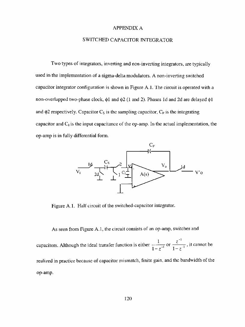
APPENDIX A
SWITCHED CAPACITOR INTEGRATOR
Two types of integrators, inverting and non-inverting integrators, are typically
used in the implementation of a sigma-delta modulators. A non-inverting switched
capacitor integrator configuration is shown in Figure A.l. The circuit is operated with a
non-overlapped two-phase clock, (t)l and ^2 (1 and 2). Phases Id and 2d are delayed ^\
and (|)2 respectively. Capacitor Cs is the sampling capacitor, Cp is the integrating
capacitor and Cj is the input capacitance of the op-amp. In the actual implementation, the
op-amp is in fully differential form.
V'o
Figure A. 1. Half circuit of the switched-capacitor integrator.
As seen from Figure A.l, the circuit consists of an op-amp, switches and
1 capacitors. Although the ideal transfer function is either or r , it cannot be
\-z-' \-z-'
realized in practice because of capacitor mismatch, finite gain, and the bandwidth of the
op-amp.
120

A.l Operational amplifier finite gain and bandwidth effect
The effect of the finite gain and finite bandwidth of the op-amp is derived in this
section. The settling time of the op-amp is determined by the bandwidth of the op-amp. It
is very important for high frequency operation. The incomplete setthng will cause pole
error as well as gain error. For simplicity, a single pole system is assumed such that
— A p
A{s) = ^—^ where p^ is the open-Ioop pole location. s + p,
Following the approach similar to [46] [47] the transfer function with finite gain
and bandwidth can be derived. Assuming that the on-resistance of the switch is small
enough, hence the effect of the RC time constant is negligible, the response of the op-
V (s) — A p amp can be described as —— = ^— . Hence in the time domain
V,{s) s-\-p,
V,(0 = 4 v „ ( 0 - - ^ ^ (A.)
\ \P^ dt
The transfer function of the switched capacitor integrator is derived by the
following procedure.
(1) During sampling phase (t)i, the sampling capacitor, Cs, is charged to Vi{n - - ) ,
therefore at the end of 01, t = {n — )T , we have
ô c , ( « - y ) = C , W ( « - y ) . (A.2)
The integrator output Vo(t) can be derived by the conservation equation to yield
- C^ (Ví>(í) - y , ( 0 ) + C,V,{t) = -Cf {Vo{n-l)-V,{n -1)) + C,V,{n -1) . (A.3)
121

Replacing Vi(t) in equation A-2 with the expression in A-3, we obtain
Cf+C,
\ J
C, +C. dV (t) VoiO + ^ y ^ = C,y„(n-l)-(C^+C,)l / , ( / i- l) . (A.4)
Therefore, the output voltage is given by
Vo{t) = Vo{n-l)e ^ "''' + ^ Vo{n-l){l-e ^'^'" )
c,.+c. Cj+C,^
(A.5)
/ ' T/ /« 1\/1 ^ Cf^oP]
C,+
at the end of øl. Assuming that the closed-loop bandwidth is large enough during this
phase and since the feedback factor is close tol if the input capacitance of the op-amp is
much smaller than that of the feedback capacitance, then
1 Cf c.+c,
C/ + - ^ '- Cf+^ '-' \ VAn--) = -—Vo{n-l). (A.7)
2 A,
(2). During the integrating phase,(l)2, Cs is discharged, and Cp accumulates the charge
Qc {n — ) which is dumped from Cs- Assuming that the op-amp is fast enough that the
settling is complete at the end of ^2, t = nT, the charge conservation equation at the
inverting input node of the op-amp can be written as
122
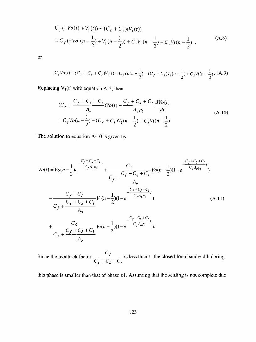
C^{-Vo{t) + V,{t)) + {C,+C,){V,{t))
= C,{-Vo'{n-^) + V,{n-^)) + C,V,{n-^)-CM{n-^) , ^^'^^
or
C,Ko(r)-(C^+C,+C,)V,(/) = C^Vo(n- i ) - (C^+C,)V,(n-- ) + C,V/(«-i) .(A.9)
Replacing Vi(t) with equation A-3, then
C.+C^+C, C. +C, +C, dVo(t) (C +-Í '-)Vo{t)-—!^ L *- ^
\ \P, dt
= CfVo{n - h - (Cf + C, )V, {n--) + C,Vi{n - -) Z^ Z A
The solution to equation A-10 is given by
Cj+Cs'rCi Cj+Cs'^Ci
Vo{t)=Vo{n-^)e ^ ^ ^ \ J^f Vo{n-^){\-e '^^^'^ \ 2 J^f ^^s^^i 2
(A.IO)
^í^^l r / . „ l ^ n „ O^oft V i ( n — ) ( l - e ^ "' ' ) (A.ll) , C ; + C , + C ; '^ 2
C , ^ / + ^ 5 + Q 2^'
Since the feedback factor is less than 1, the closed-loop bandwidth during
c,+c,+c,
this phase is smaller than that of phase øl. Assuming that the settling is not complete due
123

to the finite closed-loop bandwidth during this phase, the value Vo{n) at end of this phase
can be obtained as
_c,^c,.c,^ _c,.c,.c,^
Vo{n) = Vo{n--)e ''^'^^ + ^ + C + C ^^^^-b^^'' '^'°'" ) C , + ^ '- '-
A
Cf+C, , _ 1 C.-\-C^+C, — '• r
Cj + C , + Q + c / ' ( " - 2 * " - ^ ' > ('^•'2'
C,+Cs+C,^
+ — % ; —Vi{n--){\-e ^ "'" ) Cf+C.+C, ^ 2 '
C , + ^ í ^
where x is the duration of 02. Similarly, the expression for Vi(t) can be derived. The
output is sampled by the next stage during the coming phase ([)1. Combining those
equations and omitting the minor terms, the relationship among
Vo{n + —), Vo{n — ) and Vi{n — ) can be derived as ÂJ ÁJ JÍ^
cJyo(n+|)- c c t S F
C,A^ C,+C,+C, Vo{n-
.c.{a-«i-^';^;;^')jv,-(«-i)
C^+Q + Q ^
• ^ '
(A.13)
where £ = e ^^^"^' and T is the duration of integrating phase 02.
(3) By taking the Z-transform on Equation (A.13), the transfer function of the integrator
can be obtained as
124

(i-^)(i-:^-±i^),-. HU) = ^ ^ , (A.14)
' i - a - T ^ ^ ^—£)z-' ^ F \ ^S + C ^ + C ;
which can be rewritten as
Cs {\-a)z-'
CF \-{\~j3)z H{z)= ^. / ^ ^ '^^ _^ , (A.15)
with a = e+^'^^'^^' ^ô and ^ = - ^ + ^ s. C^A ^ C^A Cs-\-C,-\-Cj
It is seen that the transfer function is different from the ideal one. The two error
terms a, P are gain errors and pole errors, respectively. They are on the order of — and A„
C A p e~^^ where B = — is the closed-Ioop bandwidth. The effects can be reduced
by the use of high gain and wide bandwidth operational amplifiers. If A^^-^-^and B~^oo
(ideal operational amplifier), both a and P become zero and the transfer function is ideal
and is given by
H{z) = ^ - - ^ - ^ . (A.16) Cj, \ - z
A.2 Capacitor mismatch effect
The mismatch of the capacitors due to VLSI processes is considered. Capacitors
Cs and CF are not matched, the ratio can be written as
^ = C 5 + ^ ^ ^ (A.17) Cp C F -V Ôp-
125

where C's and CV are the nominal values while ôs and ôF are the errors. Since the
absolute value is not important, only the relative value, the ratio, is considered. For
C* C 4- A simplicity, assuming that—^ = -,—^, the ratio of the two capacitors becomes
Cj: C F
c, c {\^S) (A.18) c, c
where ô denotes the capacitor mismatch. Therefore the overall transfer function can be
wntten as
Cs {l-a)z-^
CF l-{l-JB)Z-'
c +c +c where a = £ + —^ '- + ô and B = ^F\ C^ -\-Cjr -\- Cj
(A.19)
£ .
It is seen that capacitor mismatch, finite gain and finite bandwidth of the op-amp
affect the gain error. The pole error is a function of only finite gain and finite bandwidth
of the op-amp. In practice, the gain error is mainly determined by capacitor mismatch.
For the high gain op-amp used, as a rule of thumb, the settling accuracy must be at least
log2(A)-\-2 bits to reduce the integrator leakage due to pole errors. With the op-amp gain
of 84 dB, for instance, the settling must be accurate to 16 bits.
126
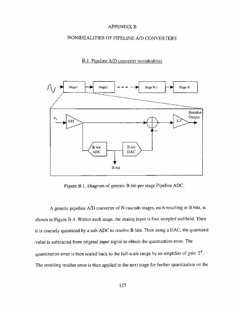
APPENDIX B
NONIDEALITIES OF PIPELINE A/D CONVERTERS
B. 1 Pipeline A/D converter nonideahties
A/Í Stagel Stage2 StageN-1 Stage N
Vi
W S / H \
/B-b i t — \ A D C
B
r
-bit
B-bit \ DAC .
• H r\ . Á -
/
w X 2 ^
Residue Output
Figure B.l. Diagram of generic B-bit-per stage Pipeline ADC.
A generic pipeline A/D converter of N cascade stages, each resulting in B bits, is
shown in Figure B-1. Within each stage, the analog input is first sampled and held. Then
it is coarsely quantized by a sub-ADC to resolve B bits. Then using a DAC, the quantized
value is subtracted from original input signal to obtain the quantization error. The
quantization error is then scaled back to the full-scale range by an amplifier of gain 2^.
The resulting residue error is then applied to the next stage for further quantization on the
127

'
1 1
1-1 V, >0
í
V, <0
next clock cycle. Due to the sample-and-hold nature of the pipehne, each stage works
concuiTently to achieve high throughput. The digital outputs of stages are combined to
arrive at the final output. For simphcity, the case where each stage resuks in one bit is
considered here. Considering the ith stage, the digital output can be written for the ideal
case as
. [1 V, > 0 (B.l)
where V,. is the input of the ith stage. The residue output voltage V^ • can be obtained by
K.,=2V,.-J,K,, (B.2)
where ±V^^j is the positive and negative reference voltages. Through successive
applications of equation (B-2), we can rewrite the input voltage of the pipeline V-^ as
^ dV • V
In practical switched capacitor circuit implementations, many factors including
capacitor mismatches, offset of comparators, offset of op-amps, finite gains and finite
bandwidth of op-amps, and charge injections degrade the performance of pipeline A/D
converters. Including the nonidealities, the above equations can be rewritten as
1 V -V >Q
-1 v^-Vo,j<o
where V^^. is the offset of the ith-stage comparator. The residue output voltage is given by
K,, ={2 + f, - 2AG,.)V, - (1 + £, - AG,)J,.^,, + y„„,,,, (B.5)
128
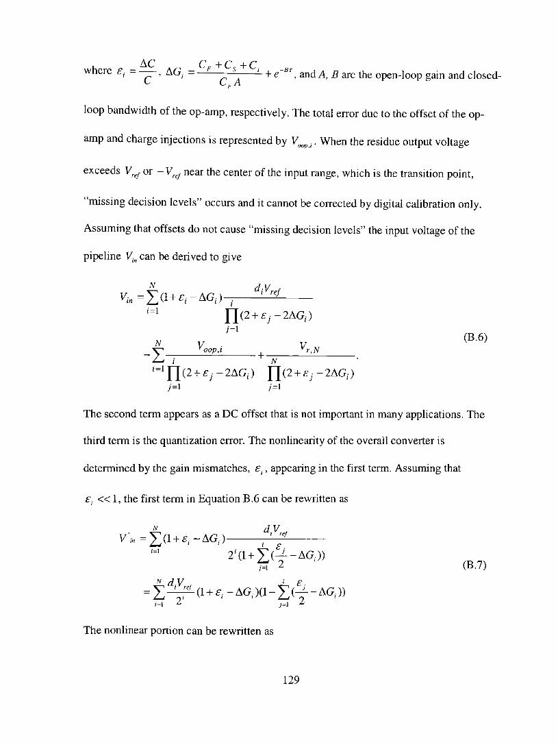
AC C -\-C -\-C where £- = —-, AG. = ^ ^ + e'^'^, and A, B are the open-Ioop gain and closed-
loop bandwidth of the op-amp, respectively. The total error due to the offset of the op-
amp and charge injections is represented by V^ .. When the residue output voltage
exceeds V^^j or -V^^j near the center of the input range, which is the transition point,
"missing decision levels" occurs and it cannot be corrected by digital calibration only.
Assuming that offsets do not cause "missing decision levels" the input voltage of the
pipeline V.^ can be derived to give
V,„ =f^{l + e,-^G,)-~^^ '•=1 r i (2+fy -2AG, )
V '"' V ^^'^
Z oop,i ^ r,N
~i ^~N •
" ^ n ( 2 + ;-2AG,) Y[{2 + £j-2^G,) ;=i / - 1
The second term appears as a DC offset that is not important in many applications. The
third term is the quantization error. The nonlinearity of the overall converter is
determined by the gain mismatches, £•, appearing in the first term. Assuming that
£. « 1 , the first term in Equation B.6 can be rewritten as
^ dV V\, = ^ ( l + ^.-AG,.) ' "'
• - ^ 2'(l + y ( ^ - A G , ) ) é 2 (B.7)
( = 1 ^ 7 = 1 ^
The nonlinear portion can be rewritten as
129

^ dV
í"=i (B-8)
If the open-Ioop gain and closed-Ioop bandwidth are large enough such that gain
mismatches of stages do not depend upon the op-amp, the nonlinear portion can be
simplified to
v,=Z ^ dV
"•i^ ref
1=1 2' (B-9)
Assuming that ^,is random with normal distribution function, N(0, a), the mean of V^
and its variance can be obtained as
E{V,}=0 (B.io)
and
Var{V,}< (Vr.CT)' ref
(B.l l)
respectively, where N is the number of bits as well as the number of stages.
B.2 Pipelined A/D converters with redundancv signed digit (RSD) technique
Pipelined A/D converters are often implemented by one bit resolution per stage as
described in the previous section. Its major disadvantage is that it cannot tolerate greatly
the offsets due to device mismatches of the comparator and op-amp, charge injections
and capacitor mismatches [48]. The error due to "missing decision levels" resulting from
those offsets, charge injections and capacitor mismatches cannot be corrected. To
eliminate this problem, pipelined A/D converters with redundancy signed digit (RSD)
130
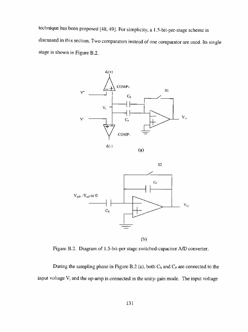
IS technique has been proposed [48, 49]. For simphcity, a 1.5-bit-per-stage scheme
discussed in this section. Two comparators instead of one comparator are used. hs single
stage is shown in Figure B.2.
v^
V
di(+)
di(-) (a)
Vr,i
S 2
Vref, -VrefOrO
Vr,i
(b)
Figure B.2. Diagram of 1.5-bit-per stage switched-capacitor A/D converter.
During the sampling phase in Figure B.2 (a), both Cs and Cp are connected to the
input voltage Vi and the op-amp is connected in the unity-gain mode. The input voltage
131

to the ith stage Vi is compared with two levels, V+(0 < V+ < VREF/2) and V (-VREF/2 < V.
< 0) neither of which needs to be accurate. For simplicity of discussion, the bit decisions
from two comparators are represented by three values J, = 7, 0, and -1 as follows:
d.
1 V^>V^
0 y - <V. <V^ (B.12)
-1 v<v-
During the multiply-by-two {Mx2) phase, CF is connected to the output, and Cs
is connected to Vrep 0, or -K^f depending on the bit decision made in the first phase, as
shown in Figure B-2 (b). The residue output voltage for the ith stage in an ideal case is
K,,. = 2 V , - d , y „ , , (B.13)
where di = +7, 0, or -1. The ideal residue plot is shown in Figure B.3. Note that the
residue output never gets close to ±Vref^i code transition points. Thus, missing decision
levels, which result when the residue output exceeds ±Vref^t code transition points, are
prevented. Therefore, the digital error correction is inherent in this algorithm, and any
offset error less than ±1/4 VrefOm be corrected- Therefore, the major advantage for the
1.5-bit-per-stage pipeline A/D converter is that it provides a high tolerance to offsets, up
to ±1/4 Vref. If Vref is IV, thc tolcrance is equal to ±250mV.
132
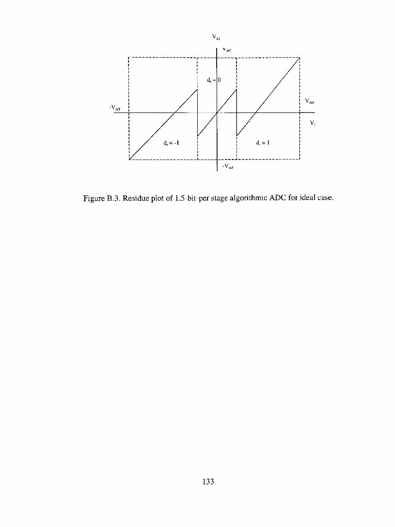
Vr.i
Vref j /
Í / '*'""'
d,=
Vref
0
- A
/ \ ^ref
/ 1 * Í d i = l Í
-V„f
Figure B.3. Residue plot of 1.5-bit-per stage algorithmic ADC for ideal case.
133
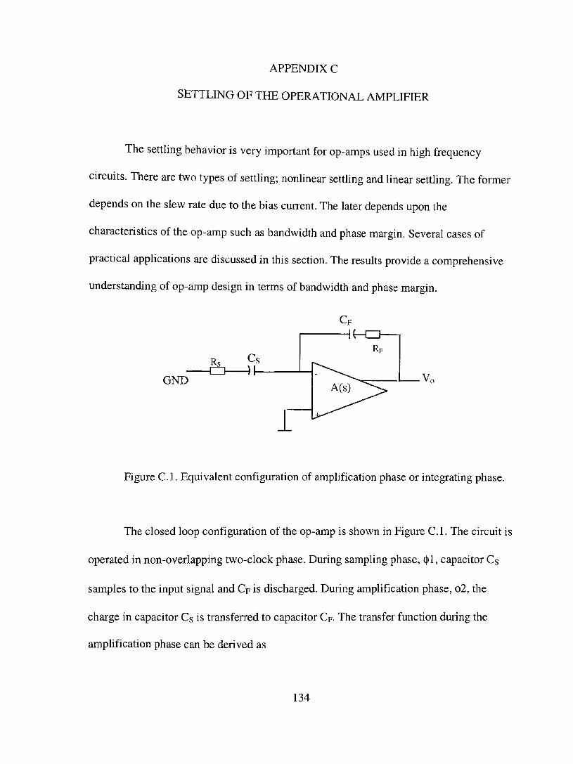
APPENDIX C
SETTLING OF THE OPERATIONAL AMPLIFIER
The settling behavior is very important for op-amps used in high frequency
circuits. There are two types of settling; nonlinear settling and linear settling. The former
depends on the slew rate due to the bias current. The later depends upon the
characteristics of the op-amp such as bandwidth and phase margin. Several cases of
practical applications are discussed in this section. The results provide a comprehensive
understanding of op-amp design in terms of bandwidth and phase margin.
GND
Figure C.l. Equivalent configuration of amplification phase or integrating phase.
The closed loop configuration of the op-amp is shown in Figure C.l. The circuit is
operated in non-overlapping two-clock phase. During sampling phase, (t)l, capacitor Cs
samples to the input signal and CF is discharged. During amplification phase, (t)2, the
charge in capacitor Cs is transferred to capacitor CF- The transfer function during the
amphfication phase can be derived as
134
H ^,)-Cs(l + sR,C,) k{s)A{s)
C,{l + sR,C,){l + k(s)A{s))
where k{s) — ^ ^ is the feedback factor. If the on-resistances of ^ + ^ + c
sR,,C,+\ sR,C,+\ '
the switches, Rp and Rs, are negligible, the feedback factor can be written as
C k{s) = - -^ . (C.2)
c,+c,+c.
C.l Single-pole svstem
Suppose the open-Ioop transfer function is of first order. (This is the case when
the phase margin is close to 90 degrees, that is, the non-dominant poles and zeros are
much greater than the unit-gain frequency.):
H^{s)=^^. (C.3) s-\-co^
where A is the open loop gain and s = -æ is the open-Ioop pole. For simplicity, the
radian frequency is used as frequency in this section.
Assuming the feedback factor of k(s), the closed loop transfer function becomes
H^{s) = '-^ . (C4) s-^{kA^-\-\)co^
135

The closed loop bandwidth is obtained as (kA^^ +1)^ . The unit-step response is given by
n(r)--^(l-e-*^^^'^'^^^). (C.5) A^ +1
It is easily derived that the settling time t = (kA »1), where N is the number k\co^
of bits for settling accuracy. Note that A^co^^ is the location of the unit-gain frequency.
The closed-loop pole is located at frequency of (kA-\-l)cOp ihãt is about k times of the unit-
gain frequency. This is why unit gain frequency is an important parameter in the op-amp
design.
C.2 Two-pole system
Suppose that the open-Ioop transfer function is of second order:
HAS)= "^""-'^-^ • (C.6) {S + (0^,)(S + ÛJ^,)
The overall closed-loop transfer function is given by
H (s) = - , ^ ° " - ' " - - . (C.7) s^ + (û> i + Cû^,)s + (kA^ + \)cú^,ú)^,_
Equation (C.7) can be written as
HSs) = ^ ^ - "^ 7 , (C.8) k\+\ s" +2C(û^s + a);
136

where the characteristic frequency í y / = (M,, + \)a}^,û}^,_ and damping factor
í ^pi
^^pÃjô^i It is inferred that ^ depends on the ratio of frequency location of the
first non-dominant pole and the frequency location of the dominant pole.
The phase margin that describes the stability of the op-amp in the closed-loop
case is defined as
PM = arctan (C.9)
where ft>„Js the unit-gain frequency. The relationship the between damping factor, ^ ,
and the phase margin (open loop) is given by
^ sin(PM) ^^^ ^ ^ ^ arccos(Vl + 4 ^ ' -2^)-2Vcos(PM)
(C.IO)
The unit-step response of the two-pole system can be easily derived for ^ l , £=1,
and E,<1.
(1). If ^ > 1, the unit step response is
M y{t) = "
M , + l 1 +
0).
2 V ^ e
K'^ (C.U)
where s^ = (^ + V^^ ~ 1 j ^ ^ ^^^ ^i ~ i^ ~ V^^ ~ 1 j^n • Therefore the setthng time can be
derived. Note that there is a slow component due to Siwhich is approximately the unit-
gain frequency of the op-amp. If ^ is much greater than 1, this case becomes case 1.
137

(2). If ^ = 1 (PM=76°), the unit step response is
kA r 1
>'( ) = ^ [ i - ^ " ' " " ' ( i + ^ . 0 ] -
In practical apphcations, ^ cannot be exactly equal to 1.
(3). If 0<^<1 (in op-amp designs, this is the usual case), the step-response is
(C-I2)
y{t) ÂAQ
M „ + l
-^û)„t
V ^ sm
í n—^^
coj-\-iein
JJ
(C.13)
Note that ^^^0^= —co^ which is usually greater than kA^p^, the closed-Ioop bandwidth of
a single pole system.
For the error of settling (consider only the envelop) we have
1 ^o e e{t) = +
-^w„t
M +1 M +1 V i ^ (C-14)
1 2 The time constant is equal to . For an N-bit settling (assuming M^ is large
enough, for example, kAo is 10 times 2^ ), we have
e ^ -N
The settling time can be then described as
(C.15)
^ ^ i V l n 2 - - l n ( l - ^ ^ ) 2 ^ ' ^OJn
(C.16)
Usually the optimal settling occurs at ^ =0.7-0.9 which corresponds to a phase margin of
60°-70°.
138

C.3 Two-pole and one-zero system
In addition to the two poles, a zero is added to the open-Ioop system such that
\co^,co p2
H{s) =
1 + 0)
i J
(5 + Û ; ^ . ) ( 5 + ^ „ 2 ) P2
then the closed-Ioop transfer function becomes
k\CÚ^,CO^^ + kA^Cú,^ co,^ s
H,{s) CÚ.
5^ + ^ co co ^ co^, -\-co^^ + ^ ^ MQ P\ P2
co. ^ + ^ n ^ P i ^ ^ + ^ )
Equation C.18 can be rewritten in the standard form
(C.17)
(C.18)
û). 1 +
HAs) = O).
V ^ ^ i y
s'^ +2^æ^s-\-o)^ 2 '
(C.19)
where ^ = and co^ =æ æ \ . 2 0)^ ^
This is the practical case for an op-amp used in the switched capacitor circuit. It is
the so-called "doublet" if the zero is close or precedes the location of the first non-
dominant pole. The analysis of the unit step response is similar to that of the two-pole
system. For simplicity, only the analysis for 0 < ^ < 1 is derived. The unit step response
(assuming that kAo is large enough such that the settling error due to the finite gain can be
neglected) can be obtained is as
139

y(-t)-l-j=={sm{coj + 4 \ - ^ ^ : l
" -"{cú,+ø). (C.20) ^ -
cosl ^z\
The envelop of the response is described by
e-^''"' co.~-2^com,-{-co^-I J — ^ ^ ~ . (C.21)
If \co_y\ « co^ and the zero is in the right-hand of the s-plane, the time constant
(^co^ becomes smaller and the magnitude is larger than that of the all-pole system. The
settling process becomes slow resulting in a long setthng time. (if co^^ is located in the
right-hand-side of the s-plane the settling process becomes slow because of small ^and
the larger square root term that results). The linear settling time tscan be derived from
Equations C.20 and C.21.
C.4 Cascode-compensated op-amp gain stage settling
The above derivations are based on the assumption that the closed loop system is
either a single-pole or two-pole system. That is to say, the other poles and zeros are in the
very high frequency range. In practice, the cascode op-amp produces four poles and three
zeros. The simplified open-Ioop transfer function in Equation 7-10 shows three poles and
two zeros. Assuming that the open-Ioop function is given by
A„(i-4) H^{s) í , (C.22)
(1 + ^ ) ( 1 + —)(1 + — ) PÍ Pi P3
the closed-loop transfer function can then be derived as
140
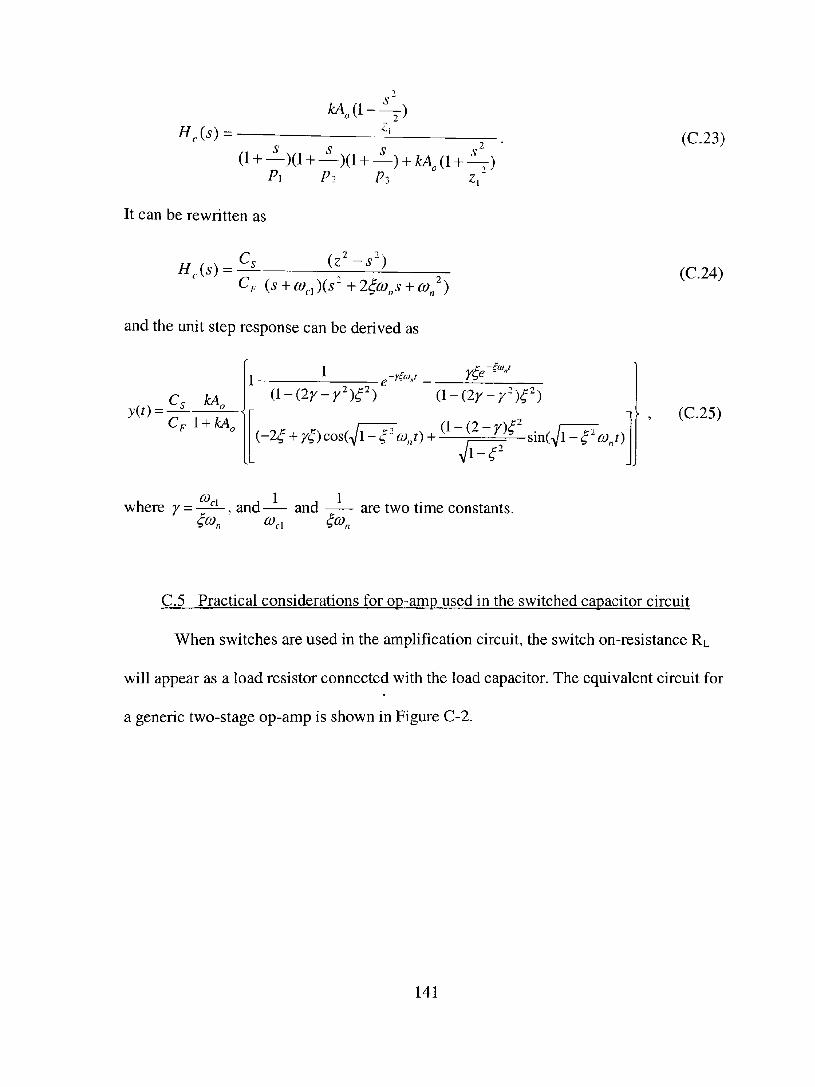
H,{s) kAo^-—)
(1 + —)(1 + —)(l + ^ ) + M„(l + - ^ ) p^ Pi Pi zr
It can be rewritten as
HAs)=^' {z'-s')
C, {s + co,^)(s-+2^co„s + û)^^)
and the unit step response can be derived as
y{t) = Cp \ + kA^
.-ríatj Y^e •i'0,,1
2 \ e 2 ( l - (2r- rOÍO (\-(2Y-y')e)
(-2^ + Y^) cos(,ir^co„t) + - ( L ( U £ s i n ( V ^ í y „ í )
where y = ——, and and are two time constants.
(C-23)
(C.24)
(C.25)
C.5 Practical considerations for op-amp used in the switched capacitor circuit
When switches are used in the amplification circuit, the switch on-resistance RL
will appear as a load resistor connected with the load capacitor. The equivalent circuit for
a generic two-stage op-amp is shown in Figure C-2.
141

gmlVÍ
Cc
Ht-
Off+ o gm^Vi
ri" Co C L
Figure C.2. The equivalent circuit of a two-stage op-amp.
The open-loop transfer function is
^(^) = \{8^2-sCc){\ + sR,C,)
(1 + A ) ( I + JL) Pi Pi
(C.27)
where />, = 8og O ô l ( 5 ' § 1 « ,?^2)
^^''-qíqTQl m2
Cc + 8.2RLC,+C,
If Ci=0 is assumed, then
Pi = 8,
Q a + ^ . 2 ^ j (C.28)
The dominant pole, pi, does not change but the non-dominant pole, p2, is shifted
to a lower frequency due to the term ^mi^LCi i" * he denominator. The extreme case
happens when Ri is large enough such that / ? ^ » , then p^ = . The phase
8m2 ^LCL
margin may increase due to the added zero caused by RL and CL- This is very different
from single stage op-amps such as folded cascode or telescopic cascode op-amps. In the
142

single stage op-amp, the load resistance and capacitance affect the dominant pole rather
than the non-dominant pole.
The closed-loop transfer function is given by
Cf kA(s) HAs) =
C, M(5) + l (C.29)
where k is the feedback factor. Omitting the zeros in the RHS of the s-plane (due to the
compensation capacitor) we have
HAs) = C _Cf co„'{\ + sR,C,)
C, s-+s{\ + KA^p,R,C,^)p,+KA,p,p, C, í -+2^íy„+íy„ '
K\p^p^{\ + sR,C^) , (C.30)
where â = — 2
C,(C,+C,) c.
+ 8m2R,CL+C,
k \ 808] (C.31)
8m2^C
and co^ = jkA^p^p^ • Assuming that Ci is much smaller than Cc and CL, then
2
8m20- + z ) c,
CLCÍ + ^ M (C.32)
kA 808 o ^
8m2^ m2 C
In practice, k<l, gmi is smaller than gm2 and CL and Cc are of the same order. The
damping factor ^ becomes smaller as compared with the condition in which RL=0. For
example, when the non-dominant pole p^ = P^QI^ where p2o is the non-dominant pole at
RL=0, to keep the damping factor unchanged requires that K\p^R^C^ = \.l^hQ settling
143

becomes slower because the natural frequency O)^^ decreases. It is predicted that the
settling becomes worse when RL increases. The Spice circuit simulation results have
verified the prediction. When RL is small, the settling is good without ringing. The
ringing becomes obvious when RL increases. To achieve fast settling, the switch on-
resistance must be as small as possible. However, the small on-resistance requires a large
size transistor that in tum introduces large parasitic capacitance appearing as load
capacitance. Therefore, care must be taken in choosing the switch size in order to get the
optimal settling. The transient response can be derived accordingly.
144
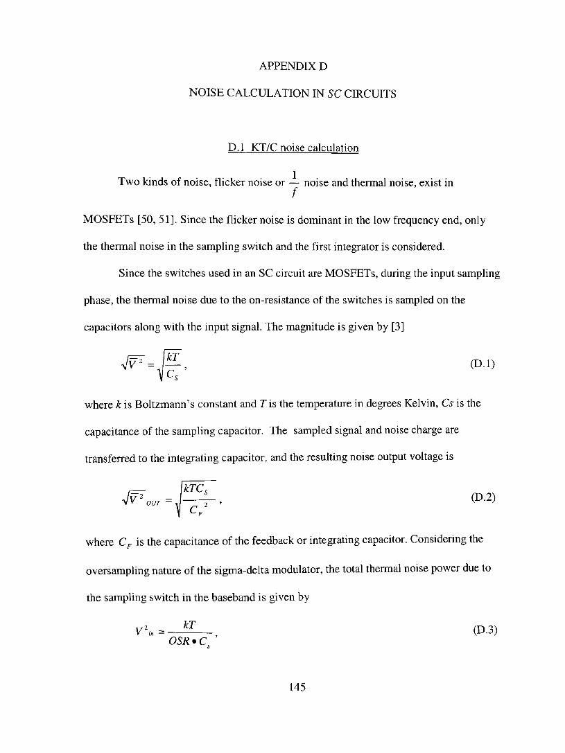
APPENDIX D
NOISE CALCULATION IN SC CIRCUITS
D.I KT/C noise calculation
Two kinds of noise, flicker noise or — noise and thermal noise, exist in
MOSFETs [50, 51]. Since the flicker noise is dominant in the low frequency end, only
the thermal noise in the sampling switch and the first integrator is considered.
Since the switches used in an SC circuit are MOSFETs, during the input sampling
phase, the thermal noise due to the on-resistance of the switches is sampled on the
capacitors along with the input signal. The magnitude is given by [3]
kT
where k is Boltzmann's constant and Tis the temperature in degrees Kelvin, Cs is the
capacitance of the sampling capacitor. The sampled signal and noise charge are
transferred to the integrating capacitor, and the resulting noise output voltage is
kTCs
where C^ is the capacitance of the feedback or integrating capacitor. Considering the
oversampling nature of the sigma-delta modulator, the total thermal noise power due to
the sampling switch in the baseband is given by
y^n = ^^ , (D.3) OSR • C„
145
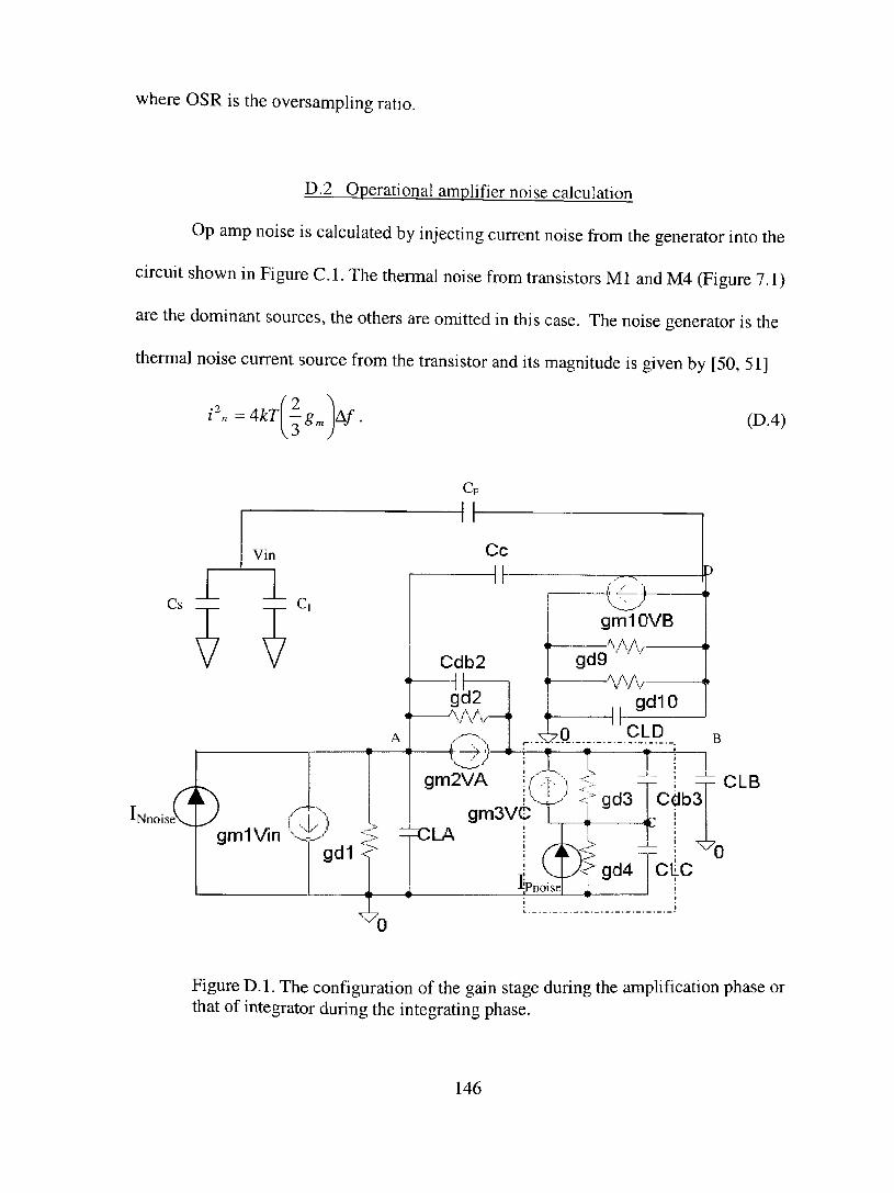
where OSR is the oversamphng ratio.
D.2 Operational amplifier noise calculation
Op amp noise is calculated by injecting current noise from the generator into the
circuit shown in Figure C.l. The thermal noise from transistors Ml and M4 (Figure 7.1)
are the dominant sources, the others are omitted in this case. The noise generator is the
thermal noise current source from the transistor and its magnitude is given by [50, 51]
r„ = 4kT A/. (D.4)
Cs
J Nnoise v . ^
Vin
Ci
V V
Z' gmlVin 'vX-'
Cc
Cdb2
gd2
gd9
gmlOVB
-vvv-gd10
CLD
gm2VA
. . ^ Q
r^—
= H C L A gm3VG 'T 1
gd1
D
(î-) gd3 • ; ^ CLB Cdb3
\7,
Pnoise gd4
0 CLC
Figure D.l. The configuration of the gain stage during the amplification phase or that of integrator during the integrating phase.
146
The thermal noise current sources //v„ /v, and Ipnoise are given by
/ ' Nnoise = AkT 8 m\ A / , (D.5)
/ Pnoise = 4kT -8 m4 A/. (D.6)
To simplify the calculation, a single pole is assumed without loss of generality.
Since a single-pole system gives more bandwidth than a multi-pole system, the thermal
noise power calculated in this case is over estimated. The output noise voltage due to the
op-amp in the gain configuration can be calculated by integrating the noise power
spectral density over the entire frequency range to yield
out
where rj =
3 Q 7
C
1 + ' 8 " '
o m4
V 8m\ J
(D.7)
c,+c,+c. and Ci is the input capacitance of the op-amp.
The output noise is first-order spectrally shaped when the op-amp is used in the
integrator of the sigma-delta modulator. Since the bandwidth of the op-amp is much
greater than the sampling frequency, high frequency noise folds into the low frequency
band when it is sampled. Assuming that noise power spectral density is uniformly
distributed in the baseband, the input referred noise voltage is thus given by
2kT
V
2n
OSR - 2 s i n
' n ^^
OSR \KJOl\Jj ( ^ \
^nc, c c
1+ ( \
6m4
V 8m\ J
(D.8)
147

Since the transconductance K of NMOS is usually three times that of PMOS, the second
term ^^^^ ( (1 . The equation can be rewritten as V Sm\ J
2kT
V
2n
OSR -2s in
^ n ^^
OSR \WOI\JJ
3TJC,
^C ^ V C
(D.9)
D.3 Total input referred noise
The total input referred noise power can be calculated by adding KT/C noise and
op-amp noise together by assuming the two noise sources are uncorrelated. The total
input referred noise is thus given by
2kT
V
2n 2sin
n ^^ OSR \KJOlVJJ
Total 3riC,
' C ^
\Cs j +
kT
OSR^C (D.IO)
For fully differential implementation of the circuit, the input referred noise voltage
increases by a factor of two assuming no correlation between the noises from the positive
side and negative side of the circuit. The total noise voltage can be derived as
AkT
V Total,diff
2n
~dsR 2sin
^ n ^^ OSR y^oixjj
í^ \
3r}C,
C,
\Cs j +
2kT
OSR • C (D.ll)
148
Related Documents