IEEE JOURNAL OF SOLID-STATECIRCUITS, VOL. 31, NO. 12, DECEMBER 1996 1995 A 660 MB/s Interface Megacell Portable Circuit in 0.3 pm-0.7 pm CMOS ASIC Kevin S. Donnelly, Associate Member, ZEEE, Yiu-Fai Chan, Member, ZEEE, John T. C. Ho, Chanh V. Tran, Samir Patel, Benedict Lau, Jun Kim, Pak Shing Chau, Charlie Huang, Jason Wei, Leung Yu, Richard Tarver, Rakhee Kulkarni, Don Stark, Member, ZEEE, and Mark G. Johnson, Member, ZEEE Abstruct- A byte-wide U0 cell with 660 MB/s data rate uses low-jitter DLL-generated clocks, self-calibrated controlled- current drivers, and linear amplifier input receivers. The CAD techniques developed allow the design to be ported to CMOS processes ranging from 0.7 pm to 0.3 pm. The chip is 0.9 x 3.4 mm2 using 0.3 pm rules. I. INTRODUCTION ICROPROCESSOR and graphic-processor speeds con- M tinue to increase dramatically, with I/O and memory bandwidths becoming a limiting factor in system performance. A high-speed DRAM device was previously reported that utilized small-swing signalling to enable extremely high data transfer rates [1]. This created the need for an I/O circuit to enable UP or ASIC connections to this DRAM. This paper describes a high-speed interface circuit that has been implemented as a byte-wide bus interface cell [2]. The I/O circuits deliver 660 Mb/s per wire, and the byte- wide interface cell therefore delivers 660 MB/s. To minimize problems caused by clock-to-data skews, two delay-locked loops (DLL’s) are used to control the timings of incoming and outgoing data. For high-speed signal transmission, low- swing controlled-current output drivers are used to reduce output switching noise and signal reflections. A novel linear amplifier input receiver is used to sample the low-swing input data. The circuits are designed to perform well in high- noise environments such as microprocessors, and to withstand L dI/dt noise generated in high-inductance packages such as PQFP’s. The interface is implemented as a full-custom ASIC library megacell, yielding area and power advantages over gate array approaches [3]. An advanced CAD methodology is used to easily port the analog circuits and high-speed digital circuits in the interface cell to multiple fabrication process technologies. The cell has been used as an interface for ASIC-to-DRAM communication as well as for ASIC-to- ASIC communication, for point-to-point links as well as for bussed links. 11. DESCRIPTION OF THE INTERFACE Fig. 1 is a block diagram of the interface cell. There are nine identical I/O cells in the interface, allowing an 8-b byte plus Manuscript received May 23, 1996. The authors are with Rambus Incorporated, Mountain View, CA 94040 Publisher Item Identifier S OOlS-9200(96)OSOS6-9. USA. parity interface. The high-speed external I/O pins appear on the right-hand side of the block diagram, while the lower-speed internal ASIC interface appears on the left-hand side. When transmitting data, 8 b of output data are latched into an register and then shifted out at the system clock rate (1.5 nsh). With nine I/O cells and 8 b of data each, 72 b of transmit data are supported at the ASIC interface. When receiving data, the input sampling circuit receives data continuously on each edge of the system clock and stores the last eight consecutive samples in a shift register. The 72 b of receive data are then made available at the ASIC interface. An f/4 ASIC clock (SynClk) is generated by the cell (from the system clock) and supplied to the internal circuits of the ASIC or the processor core. The lower frequency and wider datapath are used for the internal logic of the ASIC or processor that would have a difficult time running at the 660 MB/s data rate [4], [5]. All timings at the ASIC interface are with respect to SynClk. 111. INTERFACE TIMING An external 330 MHz clock source supplies the system clock to the interface, with data transferred on both edges of the clock. The interface cell uses low-jitter DLL circuits to control data timing. The DLL used is derived from a previously reported design [6] shown in Fig. 2. Both the new and old designs generate reference clocks and use phase interpolation to generate arbitrary delays. Also, both designs use input clock amplifiers and provide active duty-cycle correction to account for nonideal system clocks. The previous work gen- erates reference clocks in quadrature by dividing the system clock frequency in half. Then, it simultaneously performs two interpolations in quadrature, and finally uses an XOR gate to double the signal frequency back to the original system clock frequency. The complete circuit-uadrature frequency divider, dual interpolators at f/2, and an XOR frequency doubler-performs the function of a phase shifter running at the full system clock frequency. The new DLL design uses at- frequency quadrature clock generation and at-frequency phase interpolation to perform the phase shifting, with no frequency divider and no need for the XOR clock-doubler. Fig. 3 shows a block diagram of the DLL design used in this work. While both DLL’s perform the same function and can give similar performance, the new DLL uses fewer components and is somewhat simpler to design. 0018-9200/96$05.00 0 1996 IEEE

Welcome message from author
This document is posted to help you gain knowledge. Please leave a comment to let me know what you think about it! Share it to your friends and learn new things together.
Transcript
IEEE JOURNAL OF SOLID-STATE CIRCUITS, VOL. 31, NO. 12, DECEMBER 1996 1995
A 660 MB/s Interface Megacell Portable Circuit in 0.3 pm-0.7 pm CMOS ASIC
Kevin S. Donnelly, Associate Member, ZEEE, Yiu-Fai Chan, Member, ZEEE, John T. C. Ho, Chanh V. Tran, Samir Patel, Benedict Lau, Jun Kim, Pak Shing Chau, Charlie Huang, Jason Wei, Leung Yu, Richard Tarver,
Rakhee Kulkarni, Don Stark, Member, ZEEE, and Mark G. Johnson, Member, ZEEE
Abstruct- A byte-wide U 0 cell with 660 MB/s data rate uses low-jitter DLL-generated clocks, self-calibrated controlled- current drivers, and linear amplifier input receivers. The CAD techniques developed allow the design to be ported to CMOS processes ranging from 0.7 pm to 0.3 pm. The chip is 0.9 x 3.4 mm2 using 0.3 pm rules.
I. INTRODUCTION ICROPROCESSOR and graphic-processor speeds con- M tinue to increase dramatically, with I/O and memory
bandwidths becoming a limiting factor in system performance. A high-speed DRAM device was previously reported that utilized small-swing signalling to enable extremely high data transfer rates [1]. This created the need for an I/O circuit to enable UP or ASIC connections to this DRAM.
This paper describes a high-speed interface circuit that has been implemented as a byte-wide bus interface cell [ 2 ] . The I/O circuits deliver 660 Mb/s per wire, and the byte- wide interface cell therefore delivers 660 MB/s. To minimize problems caused by clock-to-data skews, two delay-locked loops (DLL’s) are used to control the timings of incoming and outgoing data. For high-speed signal transmission, low- swing controlled-current output drivers are used to reduce output switching noise and signal reflections. A novel linear amplifier input receiver is used to sample the low-swing input data. The circuits are designed to perform well in high- noise environments such as microprocessors, and to withstand L d I / d t noise generated in high-inductance packages such as PQFP’s. The interface is implemented as a full-custom ASIC library megacell, yielding area and power advantages over gate array approaches [3]. An advanced CAD methodology is used to easily port the analog circuits and high-speed digital circuits in the interface cell to multiple fabrication process technologies. The cell has been used as an interface for ASIC-to-DRAM communication as well as for ASIC-to- ASIC communication, for point-to-point links as well as for bussed links.
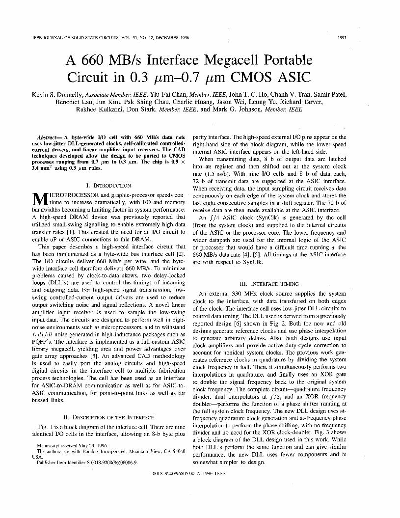
11. DESCRIPTION OF THE INTERFACE Fig. 1 is a block diagram of the interface cell. There are nine
identical I/O cells in the interface, allowing an 8-b byte plus
Manuscript received May 23, 1996. The authors are with Rambus Incorporated, Mountain View, CA 94040
Publisher Item Identifier S OOlS-9200(96)OSOS6-9. USA.
parity interface. The high-speed external I/O pins appear on the right-hand side of the block diagram, while the lower-speed internal ASIC interface appears on the left-hand side.
When transmitting data, 8 b of output data are latched into an register and then shifted out at the system clock rate (1.5 nsh). With nine I/O cells and 8 b of data each, 7 2 b of transmit data are supported at the ASIC interface. When receiving data, the input sampling circuit receives data continuously on each edge of the system clock and stores the last eight consecutive samples in a shift register. The 7 2 b of receive data are then made available at the ASIC interface.
An f / 4 ASIC clock (SynClk) is generated by the cell (from the system clock) and supplied to the internal circuits of the ASIC or the processor core. The lower frequency and wider datapath are used for the internal logic of the ASIC or processor that would have a difficult time running at the 660 MB/s data rate [4], [5]. All timings at the ASIC interface are with respect to SynClk.
111. INTERFACE TIMING
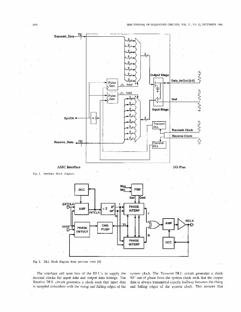
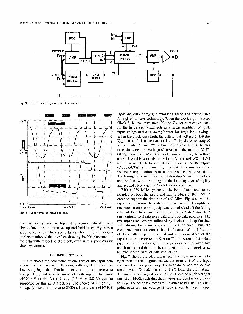
An external 330 MHz clock source supplies the system clock to the interface, with data transferred on both edges of the clock. The interface cell uses low-jitter DLL circuits to control data timing. The DLL used is derived from a previously reported design [6] shown in Fig. 2. Both the new and old designs generate reference clocks and use phase interpolation to generate arbitrary delays. Also, both designs use input clock amplifiers and provide active duty-cycle correction to account for nonideal system clocks. The previous work gen- erates reference clocks in quadrature by dividing the system clock frequency in half. Then, it simultaneously performs two interpolations in quadrature, and finally uses an XOR gate to double the signal frequency back to the original system clock frequency. The complete circuit-uadrature frequency divider, dual interpolators at f / 2 , and an XOR frequency doubler-performs the function of a phase shifter running at the full system clock frequency. The new DLL design uses at- frequency quadrature clock generation and at-frequency phase interpolation to perform the phase shifting, with no frequency divider and no need for the XOR clock-doubler. Fig. 3 shows a block diagram of the DLL design used in this work. While both DLL’s perform the same function and can give similar performance, the new DLL uses fewer components and is somewhat simpler to design.
0018-9200/96$05.00 0 1996 IEEE
1996 IEEE JOURNAL OF SOLID-STATE CIRCUITS, VOL. 31, NO. 12, DECEMBER 1996
-+ Transmit-Data
SynClk +--
+ Receive-Data
ASIC Interface
Fig. 1. Interface block diagram.
Input Stage I ' r $ q Transmit
I rl
5 Data-Inlout [8:0]
Vref $
Receive Clock *
YO Pins
EX
VR
M M
I U I ~~
Fig. 2. DLL block diagram from previous work [6].
The interface cell uses two of the DLL's to supply the internal clocks for input data and output data timings. The Receive DLL circuit generates a clock such that input data is sampled coincident with the rising and falling edges of the
system clock. The Transmit DLL circuit generates a clock 90" out of phase from the system clock such that the output data is always transmitted exactly halfway between the rising and falling edges of the system clock. This ensures that
DONNELLY et al.: A 660 MBls INTERFACE MEGACELL PORTABLE CIRCUIT
, INTERP
iNT&!- 9 0 ' 7
vc CHG b
1997
Fig. 3. DLL block diagram from this work.
input and output stages, maximizing speed and performance for a given process technology. When the clock input (labeled Clock-b) is low, transistors P3 and P 4 act as resistive loads for the first stage, which acts as a linear amplifier for small input swings and as a swing-limiter for large input swings. When the clock goes high, the differential voltage of DataIn- Vref is amplified at the nodes ( A , A-B) by the cross-coupled active loads P1 and P2 within the required 1.5 ns. At this time, the second stage is precharged and the outputs (OUT, OUTB) equalized. When the clock again goes low, the voltage at (A , A B ) drives transistors N5 and N6 through N 3 and N4 to resolve and latch the data at the full-swing CMOS outputs (OUT, OUTB). Simultaneously, the first stage goes back into its linear amplification mode to process the next even data. The timing diagram shows the relationship between the clock and the data, with the timings of the first stage sense/amplify and second stage equalizeAatch functions shown.
With a 330 MHz system clock, input data needs to be sampled on both the rising and falling edges of the clock in order to support the data rate of 660 Mb/s. Fig. 6 shows the input data-pipeline block diagram. Two identical amplifiers, one clocked off the rising edge and one clocked off the falling edge of the clock, are used to sample one data pin, with their outputs split into even-data and odd-data pipelines. The
i j
25.12ns l n s / d I u - 35* lZns
Fig. 4. Scope trace of clock and data.
the interface cell on the chip that is receiving the data will always have the optimum set up and hold times. Fig. 4 is a scope trace of the clock and data waveforms from a 0.7-pm implementation of the interface showing the 90' placement of the data with respect to the clock, even with a poor quality clock waveform.
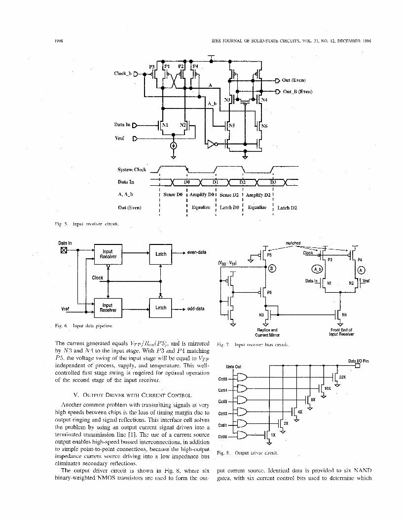
IV. INPUT RECEIVER Fig. 5 shows the schematic of one-half of the input data
receiver of the interface cell, along with signal timings. The low-swing input data DataIn is centered around a reference voltage Vref, and a wide range of both input data swing (k300 mV to f l V) and Vref (1.6 V to 2.8 V) can be supported by this input amplifier. The choice of a high Vref voltage (closer to V ~ D than to GND) allows the use of NMOS
two input receivers are followed by latches tokeep the data valid during the second stage's equalization time. Thus, the complete input cell accomplishes the functions of amplification of the small-swing input signal and sample-and-hold of the input data. As described in Section 11, the outputs of this data pipeline are fed into eight shift registers (four for even-data and four for odd-data). This completes the high-speed serial to lower-speed parallel data conversion.
Fig. 7 shows the bias circuit for the input receiver. The right side of the diagram shows the front end of the input receiver described previously. The left side forms a replica bias circuit, with P5 matching P3 and P4 from the input stage. The inverter is designed with the PMOS device much stronger than the NMOS, such that the inverter trip point is very close to V T ~ . The feedback forces the inverter to balance at its trip point, such that the voltage at node B equals VDD - VTP.
1998 IEEE JOURNAL OF SOLID-STATE CIRCUITS, VOL. 31, NO. 12, DECEMBER 1996
4"
Fig. 5. Input receiver
Out (Even)
Out-B (Even)
System Clock I I I I
Data In I I I I I
A, A-b I SenseDO I AmplifyDOI SenseD2 1 AmplifyD2 I I I I I I
I Out(Even)
I I I I I
I Equalize Latch DO f Equalize , LatchD2 I
circuit.
even-data
odd-data
Fig. 6. Input data pipeline.
The current generated equals V T P / R ~ ~ ( P5), and is mirrored by N 3 and N4 to the input stage. With P3 and P 4 matching P5, the voltage swing of the input stage will be equal to VTP independent of process, supply, and temperature. This well- controlled first stage swing is required for optimal operation of the second stage of the input receiver.
v. OUTPUT DRIVER WITH CURRENT CONTROL
Another common problem with transmitting signals at very high speeds between chips is the loss of timing margin due to output ringing and signal reflections. This interface cell solves the problem by using an output current signal driven into a terminated transmission line [l]. The use of a current source output enables high-speed bussed interconnections, in addition to simple point-to-point connections, because the high-output impedance current source driving into a low-impedance bus eliminates secondary reflections.
The output driver circuit is shown in Fig. 8, where six binary-weighted NMOS transistors are used to form the out-
matched
(
* Replica and
Current Mirror
* Fig. 7. Input receiver bias circuit.
* Front End of
Input Receiver
Data WO Pin Data Out
Cct15
cctw
Cctl3
CctlZ
CCtlO ( 1 x Ts
Fig. 8 . Output driver circuit
put current source. Identical data is provided to six NAND gates, with six current control bits used to determine which
DONNELLY et al.: A 660 MBls INTERFACE MEGACELL PORTABLE CIRCUIT
1
1999
For CCTL Pin
Fig. 9. Current-control circuit.
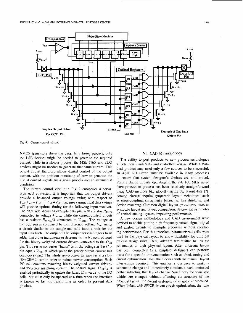
NMOS transistors drive the data. In a faster process, only the LSB devices might be needed to generate the required current, while in a slower process, the MSB (16X and 32X) devices might be needed to generate that same current. This output circuit therefore allows digital control of the output current, with the problem remaining of how to generate the digital control signals for a given process and environmental condition.
The current-control circuit in Fig. 9 comprises a servo- type A/D converter. It is important that the output drivers provide a balanced output voltage swing with respect to Kef( Voh- Kef = Kef - Val), because symmetrical data swings will provide optimal timing for the following input receiver. The right side shows an example data pin, with resistor Rtelm connected to voltage V,,,,, while the current-control circuit has a resistor Rterm/2 connected to V,,,,. The voltage at the Cctl pin is compared to the reference voltage Vref using a circuit similar to the sample-and-hold input circuit for the input data latch. The output of the comparator circuit goes to an adder that either increments or decrements the 6 b control word for the binary-weighted current drivers connected to the C,., pin. This servo converter “hunts” until the voltage at the Cctl pin equals Vref, at which point the proper output current has been developed. The whole servo converter samples at a slow (SynClW32) rate in order to reduce power consumption. Each I/O cell contains matching binary-weighted current drivers, and therefore matching current. The control signal CctlLd is enabled periodically to update the latest Cctl value to the I/O cells, but must only be updated at a time when the interface is known to be not transmitting in order to prevent data glitches.
VI. CAD METHODOLOGY The ability to port products to new process technologies
affects their availability and cost-effectiveness. While a stan- dard product may need only a few sources to be successful, an ASIC I/O circuit must be available in many processes to ensure that system designer’s choices are not limited. Porting digital circuits operating in the sub 100 MHz range from process to process has been relatively straightforward using CAD methods like globally sizing the layout data [7]. Analog circuits require symmetric layout techniques, such as cross-coupling, capacitance balancing, line shielding, and device matching. Common digital layout procedures, such as symbolic layout and layout compaction, destroy the symmetry of critical analog layouts, impacting performance.
A new design methodology and CAD environment were devised to enable porting high frequency mixed-signal digital and analog circuits to multiple processes without sacrific- ing performance. For this interface, parameterized cells were used in the physical layout to allow flexibility for different process design rules. Then, software was written to link the schematics to their physical layout. After a circuit layout has been completed as a template, designers can perform tasks for a specific implementation such as clock tuning and circuit optimization from their desks with no manual layout intervention required. This enables a designer to make a schematic change and immediately simulate a back-annotated netlist reflecting that layout change. Since only the transistor widths are changed without affecting the structure of the physical layout, the circuit performance is not compromised. When linked with SPICE-driven circuit optimization, the time
2000 IEEE JOURNAL OF SOLID-STATE CIRCUITS, VOL 31, NO 12, DECEMBER 1996
B ’ TEMPLATE SHRINK TEMPLATE SHRINK DESIGN
Fig. 10. Layout template example
required to port the interface to a new process technology is drastically reduced.
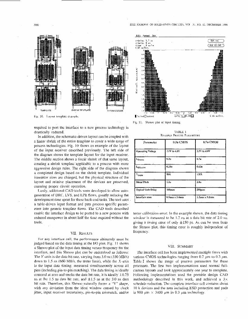
In addition, the schematic-driven layout can be coupled with a linear shrink of the entire template to cover a wide range of process technologies. Fig. 10 shows an example of the layout of the input receiver described previously. The left side of the diagram shows the template layout for the input receiver. The middle section shows a linear shrink of that same layout, creating a shrink template applicable to a process with more aggressive design rules. The right side of the diagram shows a completed design based on the shrink template. Individual transistor sizes are changed, but the physical structure of the layout and relative placement of the devices are preserved, ensuring proper circuit operation.
Lastly, additional CAD tools were developed to allow auto- generation of DRC, LVS, and LPE flows, greatly reducing the development time spent for these back-end tasks. The tool uses a table-driven input format and puts process-specific param- eters into generic template flows. The CAD tools described enable the interface design to be ported to a new process with reduced manpower in about half the time required without the tools.
VII. RESULTS For any interface cell, the performance ultimately must be
judged based on the data timing at the I/O pins. Fig. 11 shows a Shmoo plot of the input data timing versus frequency for the interface, and this Shmoo plot can be understood as follows: The Y-axis is the data bit rate, varying from 3.0 ns (330 MB/s) down to 1.5 ns (660 MB/s, the tester limit), while the X-axis is the input data timing, measured simultaneously across all pins (including pin-to-pin matching). The data timing is ideally centered at zero and tracks the data bit rate; it is ideally *0.75 ns at the 1.5 ns data bit rate, and *1.5 ns at the 3.0 ns data bit rate. Therefore, this Shmoo naturally forms a “V” shape, with any deviation from the ideal window caused by clock jitter, input receiver uncertainty, pin-to-pin mismatch, and/or
x-delta: 1.1 ns y - d e l t a : 0 ns slope : 0 ns/ns 0.02 ns/Di v.
(Get) (m)
4 0.25 7
-0.P5
I f a i l e d [ I p a s s s d l in/ ie (i_BD_B)I
Fig 11. Shmoo plot of input timing.
TABLE I EXAMPLE PROCESS PARAMETERS
1 0 . 2 4 ~ 1 0 . 6 2 ~ I
tester calibration error. In the example shown, the data timing window is measured to be 1.7 ns at a data bit rate of 2.0 ns, giving a timing error of only &150 ps. As can be seen from the Shmoo plot, this timing error is roughly independent of frequency.
VIII. SUMMARY
The interface cell has been implemented multiple times with various CMOS technologies ranging from 0.7 pm to 0.3 pm. Table I shows the range of process parameters for these processes. The first two implementations used normal full- custom layouts and took approximately one year to complete. Following implementations used the portable design CAD methodology described jn this work, and achieved a 3x schedule reduction. The complete interface cell contains about 10 k devices and the area including ESD protection and pads is 900 pm x 3400 pm in 0.3 pm technology.
DONNELLY et al.: A 660 MBIs INTERFACE MEGACELL PORTABLE CIRCUIT 2001
REFERENCES
N. Kushiyama et al., “A 500-MegaBytes/s data-rate 4.5 M DRAM,” IEEE J. Solid-state Circuits, vol. 28, pp. 490-498, Dec. 1993. K. Donnelly et al., “A 660 MB/s interface megacell portable circuit in 0.3 pm-0.7 p m CMOS ASIC,” in ISSCC Dig. Tech. Papers, Feb. 1996, pp. 290-291. T. Takahashi et al., “A CMOS gate array with 600 Mb/s simultaneous bidirectional I/O circuits,” in ISSCC Dig. Tech. Papers, Feb. 1995, pp. 40-4 1. J. Schutz, “A 3.3 V 0.6 p m BiCMOS superscalar microprocessor,” in ZSSCC Dig. Tech. Papers, Feb. 1994, pp. 202-203. W. Bowhill et al., “A 300 MHz 64b quad-issue CMOS RISC micropro- cessor,” in ISSCC Dig. Tech. Papers, Feb. 1995, pp. 182-183. T. Lee et al., “A 2.5 V CMOS delay-locked loop for an 18 Mbit, 500 Megabytesls DRAM,” IEEE J. Solid-State Circuits, vol. 29, pp. 1491-1496, Dec. 1994. J. Scbutz, “A CMOS 100 MHz Microprocessor,” in ZSSCC Dig. Tech. Papers, Feb. 1991, pp. 90-91.
Fig. 12. Die photograph.
l/O Cell Slice
Delay Locked Loops (DLts)
Clock Buffers
Control Logic
CU~PMlt COOWQl
Kevin S. Donnelly (A’93) was born in Los Angeles, CA, in 1961. He received the B.S. degree in EECS from the University of California, Berkeley, in 1985, and the M.S. degree in electrical engineering from San Jose State University, CA, in 1992.
Since 1984, he has worked at Memorex, Sipex, and National Semiconductor specializing in bipo- lar and BiCMOS analog circuits for disk drive read/write and servo channels. In 1992, he joined Rambus, Inc. of Mountain View, CA, where he has designed high-speed CMOS PLL circuits for clock
recovery and data synchronization, and high-speed 1/0 circuits He currently manages a group developing next generation PLL’s. His interests include PLL’s and DLL’s, I/O circuits, data converters, and audio circuits.
Mr Donnelly holds several circuit design patents and was co-author of the winner of the best paper award at the 1994 ISSCC
Fig. 13. Die photograph detail.
Yiu-Fai Chan (S’76-M’78) was born in Hong Kong in 1950. He received the B.S. and M.S. degrees in electrical engineering and computer sci- ences with Highest Honors from the University of California, Berkeley, in 1972 and 1973, respec- tively. He also attended the MBA program at the University of Santa Clara in 1976
Before joining National Semiconductor in 1974 as a Design Engineer working on calculator and TV game integrated circuits, he received the University Chancellor Science Fellowship at U.C. Berkeley and
did research on solid-state devices and microwave acoustics. From 1976 to 1983 he held various technical and management positions at Intersil Inc. (later became a division of General Electric) where be was engaged in the development of various CMOS memory devices, microprocessors, and peripheral devices It was at Intersil Inc. that he developed the design and technology of the first EPROM devices in a CMOS process. He joined Altera Corp. in 1983 where he led a team of engineers to develop the industry’s first CMOS Drogrammable logic devices. In 1991 he was at Tera Microsvstems in
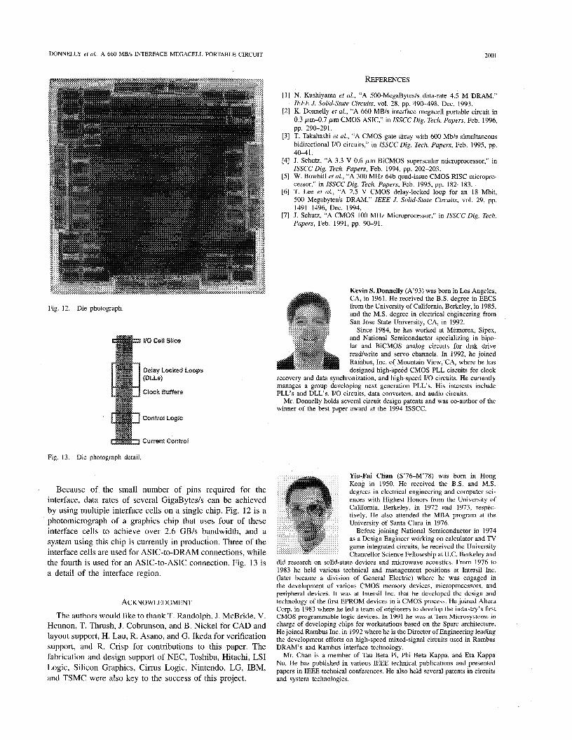
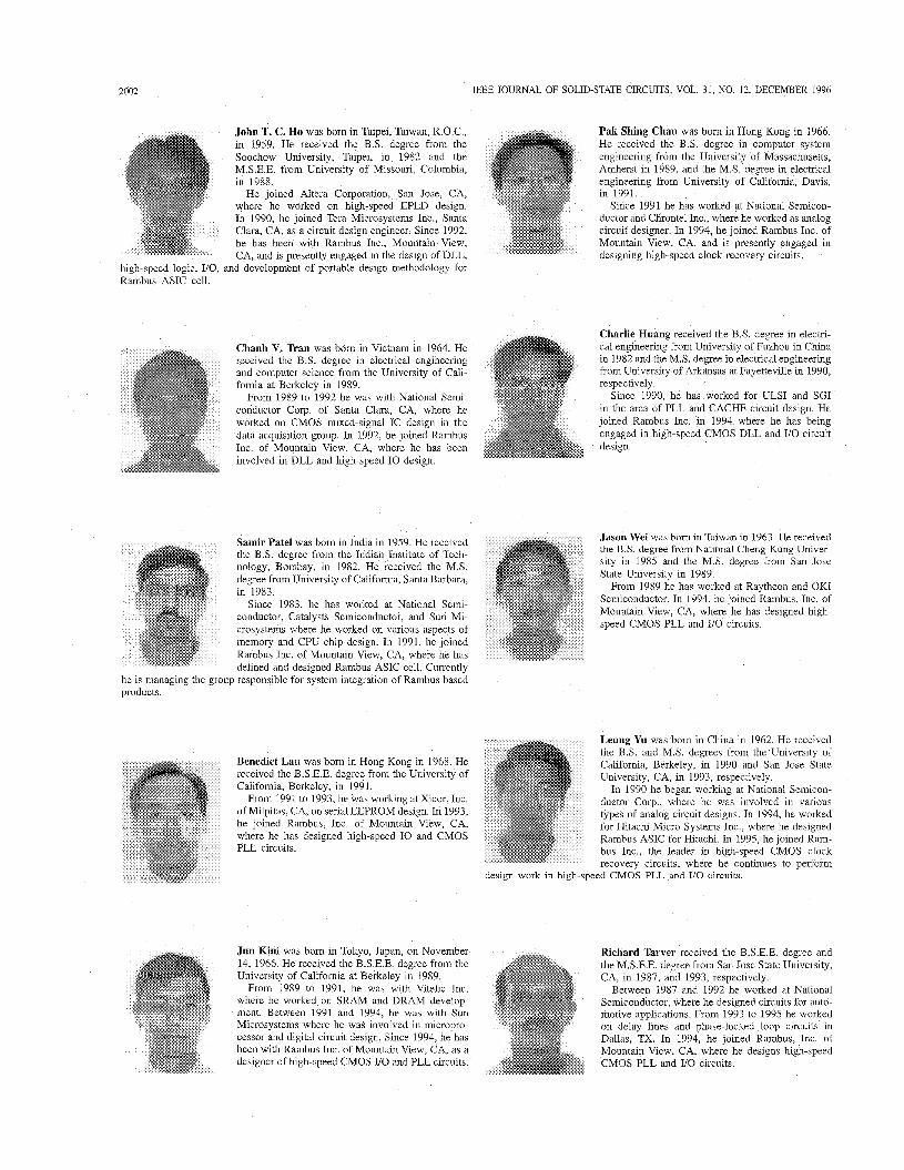
Because of the small number of pins required for the interface, data rates of several GigaBytes/s can be achieved by using multiple interface cells on a single chip. Fig. 12 is a photomicrograph of a graphics chip that uses four of these interface cells to achieve over 2.6 GB/s bandwidth, and a system using this chip is currently in production. Three of the interface cells are used for ASIC-to-DRAM connections, while the fourth is used for an ASIC-to-ASIC connection. Fig. 13 is a detail of the interface region.
ACKNOWLEDGMENT The authors would like to thank T. Randoluh. J. McBride. V.
I Y U
Hennon, T. Thmsh, J. Cobmnson, and B, Nickel for CAD and layout support7 H. Lau, R. Asan’, and G. Ikeda for verification
charge of developing chips for workstations based on the sparc architecture He joined Rambus Inc in 1992 where he is the Director of Engineering leading the development efforts on high-speed mixed-signal circuits used in Rambus DRAM’S and Rambus interface technology support, and R. Crisp for contributions to this paper. The
fabrication and design support of NEC, Toshiba, Hitichi, LSI Nintendo, LG7 IBM,
Mr. Chan is a member of Tau Beta Pi, Phi Beta Kappa, and Eta Kappa Nu. He has published in various IEEE technical publications and presented papers in IEEE technical conferences. He also held several patents in circuits _ _
and TSMC were also key to the success of this project. and system technologies.
2002 IEEE JOURNAL OF SOLID-STATE CIRCUITS, VOL 31, NO. 12, DECEMBER 1996
John T. C. Ho was born in Taipei, Taiwan, R .0 C , Pak Shing Chau was horn in Hong Kong in 1966. in 1959. He received the E S. degree from the He received the B.S degree in computer system Soochow University, Taipei, in 1982 and the engineering from the University of Massachusetts, M.S E E. from University of Missouri, Columbia, Amherst in 1989, and the M S degree in electrical in 1988. engineering from University of California, Davis,
He joined Altera Corporation, San Jose, CA, in 1991 where he worked on high-speed EPLD design Since 1991 he has worked at National Semicon- In 1990, he joined Tera Microsystems Inc., Santa ductor and Chrontel Inc , where he worked as analog Clara, CA, as a circuit design engineer. Since 1992, circuit designer. In 1994, he joined Rambus Inc. of he has been with Rambus Inc., Mountain View, Mountam View, CA, and is presently engaged in CA, and is presently engaged in the design of DLL, designing high-speed clock recovery circuits.
high-speed logic, I/O, and development of portable design methodology for Rambus ASIC cell.
Chanh V. Tran was born in Vietnam in 1964 He received the B S degree in electrical engineering and computer science from the University of Cah- fornia at Berkeley in 1989
From 1989 to 1992 he was with National Semi- conductor Corp of Santa Clara, CA, where he worked on CMOS mixed-signal IC design in the data acquisition group In 1992, he joined Rambus Inc of Mountain View, CA, where he has been involved in DLL and high-speed IO design
Samir Pate1 was horn in India in 1959 He received the B S degree from the Indian Institute of Tech- nology, Bombay, in 1982 He received the M S degree from University of California, Santa Barbara, in 1983
Since 1983, he has worked at National Semi- conductor, Catalysts Semiconductor, and Sun Mi- crosystems where he worked on various aspects of memory and CPU chip design In 1991, he joined Rambus Inc of Mountain View, CA, where he has defined and designed Rambus ASIC cell Currently
he is managing the group responsible for system integration of Rambus based products.
Benedict Lau was horn in Hong Kong in 1968 He received the B.S.E.E. degree from the University of California, Berkeley, in 1991.
From 1991 to 1993, he was working at Xicor, Inc. of Milpitas, CA, on serial EEPROM design. In 1993, he joined Rambus, Inc. of Mountain View, CA, where he has designed high-speed 10 and CMOS PLL circuits.
Jun Kim was born in Tokyo, Japan, on November 14, 1966 He received the B S E E degree from the University of California at Berkeley in 1989
From 1989 to 1991, he was with Vitelic Inc where he worked on SRAM and DRAM develop ment Between 1991 and 1994, he was with Sun Microsystems where he was involved in micropro- cessor and digital circuit design Since 1994, he has been with Rambus Inc of Mountain View, CA, as a designer of high-speed CMOS I/O and PLL circuits
Charlie Huang received the B.S degree in electri- cal engineering from University of Fuzhou in China in 1982 and the M.S degree in electrical engineering from University of Arkansas at Fayetteville in 1990, respectively
Since 1990, he has worked for ULSI and SGI in the area of PLL and CACHE circuit design He joined Rambus Inc in 1994 where he has being engaged in high-speed CMOS DLL and I/O circuit design.
Jason Wei was born in Taiwan in 1963 He received the B S degree from National Cheng-Kung Univer- sity in 1985 and the M S. degree from San Jose State University in 1989
From 1989 he has worked at Raytheon and OKI Semiconductor. In 1994, he joined Rambus, Inc. of Mountain View, CA, where he has designed high- speed CMOS PLL and I/O circuits
design work in high-spec
Leung Yu was born in China in 1962 He received the B S and M S degrees from the University of California, Berkeley, in 1990 and San Jose State University, CA, in 1993, respectively
In 1990 he began working at National Semicon- ductor Corp, where he was involved in various types of analog circuit designs In 1994, he worked for Hitachi Micro Systems Inc , where he designed Rambus ASIC for Hitachi In 1995, he joined Ram- bus Inc, the leader in high-speed CMOS clock recovery circuits, where he continues to perform
sd CMOS PLL and U 0 circuits
Richard Tarver received the B S E E degree and the M S E E degree from San Jose State University, CA, in 1987, and 1993, respectively
Between 1987 and 1992 he worked at National Semiconductor, where he designed circuits for auto- motive applications From 1993 to 1995 he worked on delay lines and phase-locked loop circuits in Dallas, TX In 1994, he joined Rambus, Inc of Mountain View, CA, where he designs high-speed CMOS PLL and U 0 circuits
DONNELLY et al.: A 660 MBIs INTERFACE MEGACELL PORTABLE CIRCUIT 2003
Rakhee Kulkarni was born in Jammu, India, in 1967. She received the B.S. degree from Regional Engineering College, Srinagar, India, in 1988 and the M.S. degree from Oregon State University, Corvallis, in 1992.
Beginning in 1992, she worked at National Semi- conductor, where she specialized in EEPROM mem- ory circuits. In 1995, she joined Rambus, Inc. of Mountain View, CA.
Don Stark (S’86-M’91) received the B.S. degree from Massachusetts Institute of Technology, Cam- bridge, in 1985, and the M.S. and Ph.D. degrees from Stanford University, Stanford, CA, in 1987 and 1991, respectively, all in electrical engineering. His research interests at Stanford included circuit design and CAD tools for analysis of voltage and current distributions in VLSI circuits.
From 1987 to 1991 he was also a member of the Digital Equipment Corporation Western Re- search Laboratory, Palo Alto, CA, working on CAD
development and ECL circuit design. From 1991 to 1993 he worked at the Semiconductor Device Engineering Laboratory, Toshiba Corporation, Kawasaki, Japan, on DRAM design. In 1993 he joined Rambus Inc., Mountain View, CA, where he currently works on DRAM, high-speed I/O design, and CAD.
Mark G. Johnson (S’78-M’83) was born in Hous- ton, TX, in 1957. He received the B.S.E.E. degree from Rice University, Houston, TX, in 1979, and the S.M. degree from Massachusetts Institute of Technology, Cambridge, in 1982.
He joined Mostek Corporation in 1982, design- ing SRAM and DRAM products in both NMOS and CMOS technology. In 1986 he joined MIPS Computer Systems where he did circuit designs for floating point chips, phase-locked loops, and high-speed backplane buses. In 1991 he designed
subnanosecond ECL FIFO circuits at MicroUnity, before joining Rambus Inc. in 1992. From 1992-1996 he designed high-speed mixed-signal circuits at Rambus, including reduced-swing U0 and PLLDLL circuits in commodity DRAM CMOS technology. He is now an independent consultant.
Mr. Johnson is a member of Sigma Xi, Phi Beta Kappa, and Tau Beta Pi.
Related Documents