Journal of Information Engineering and Applications www.iiste.org ISSN 2224-5782 (print) ISSN 2225-0506 (online) Vol.7, No.3, 2017 1 A 60nm CMOS, 3 rd and 5 th Order Low Pass Filter with Higher Cut-off Frequency Suman Nehra * P.K.Ghosh Department of Electronics and Communication, College of Engineering and Technology, Mody University of Science and Technology, lakshmangarh, India Abstract The design of CMOS based low pass filter for analog-to-digital, digital-to-analog and audio applications is described in this paper. Active load resistor and floating inductor is used for the implementation of low pass filter. CMOS technology has become dominant over bipolar technology for analog circuits design in mixed signal system. The differential floating active inductor is designed with CMOS and current sources. The floating inductor may be electronically tuned by varying external bias voltage as well as current. The simulations are obtained by using 65nm CMOS technology on Tanner EDA tool 13.0. The filters are synthesized from 3 rd and 5 th order low-pass LC prototype and designed using ladder structure. Keywords: Complementary Metal Oxide Semiconductor (CMOS), low pass filter (LPF), active resistor, Power delay product (PDP). 1. Introduction The improvement of scaled VLSI technologies, associated with the demand for signal processing integrated in a single chip, has extremely good ability for design of analog circuits. Mostly the VLSI circuits in analog consist of amplifiers, filters, oscillators, digital to analog converters and analog to digital converter [1] [2]. The key driving factor for any system is high gain, high packing density, low power dissipation, easy in designing etc. The most important part in analog circuit that should be integrated is analog filters [3] [4]. The performance of general purposed processor and digital signal processing unit has been increased by scaling of CMOS technologies. Advanced and scalable CMOS technologies provide low cost, high integration and good reliability which form digital and analog circuit in a single chip [5] [6]. Filters especially analog filters has a wide range of applications in different areas such as in control system, communication system, military, radar, medical instruments and industrial electronics [7] [8]. Filter is a circuit that transforms an electrical signal at input in such a manner so that the output signal has specified features which may be in terms of frequency or in time domain depending upon the application. Filter is the circuit that works on signal in a frequency dependent manner [9] [10]. The fundamental nature of a filter can be described by evaluating the frequency dependent behavior of the impedance of inductor and capacitor [11] [12]. Filters can be made from passive components and from active components. Filters that are fabricated from active components have large number of advantages over filters fabricated with passive components. Passive inductor is large in size, unable to work at moderate frequency range; standard values are not very close to each other [13] [14]. So active inductor is preferred for the designing of filters. In this paper section 2 describes proposed active inductor, 3 rd and 5 th order filters using active inductor. Section 3 gives the experimental results. Conclusion is in section 4. 2. Filters Proposed differential floating active inductor was designed with the help of CMOS and current sources that was shown in Fig. 1 (a) and the schematic shown in fig. 1 (b) is of conventional inductor. Proposed active inductor was designed with 7 CMOS which include 4 NMOS from M1 to M4 and 3 PMOS from M5 to M7. Cross- coupled pair was formed by M1 and M2, from dc point of view and transistors M3 and M4 are in common drain configuration. The above circuit works as an inductor at the input voltage V in . At the quiescent bias point, transistors M1 to M4 are saturated. Depending on the controlled voltages V b and V bb at the gates transistors M5, M6 and M7 they work in linear region or in saturation region. Therefore at desired bias point M5, M6 and M7 are modeled as gds5, gds5’ gds6 and gds7 representing the drain conductance. In this paper conventional inductor is the inductor that was proposed by Lu et al. [15]. In fig. 2 (a) small-signal model for the proposed active inductor in simplified manner is shown, and fig. 2(b) shows the equivalent impedance circuit of active inductor. Small-signal analysis is done for the approximate analysis of a circuit [16] [17]. For an input current I in , the input voltage is V in , for the differential port input impedance Z in is given below: (1)

Welcome message from author
This document is posted to help you gain knowledge. Please leave a comment to let me know what you think about it! Share it to your friends and learn new things together.
Transcript
Journal of Information Engineering and Applications www.iiste.org
ISSN 2224-5782 (print) ISSN 2225-0506 (online)
Vol.7, No.3, 2017
1
A 60nm CMOS, 3rd
and 5th
Order Low Pass Filter with Higher
Cut-off Frequency
Suman Nehra* P.K.Ghosh
Department of Electronics and Communication, College of Engineering and Technology, Mody University of
Science and Technology, lakshmangarh, India
Abstract
The design of CMOS based low pass filter for analog-to-digital, digital-to-analog and audio applications is
described in this paper. Active load resistor and floating inductor is used for the implementation of low pass
filter. CMOS technology has become dominant over bipolar technology for analog circuits design in mixed
signal system. The differential floating active inductor is designed with CMOS and current sources. The floating
inductor may be electronically tuned by varying external bias voltage as well as current. The simulations are
obtained by using 65nm CMOS technology on Tanner EDA tool 13.0. The filters are synthesized from 3rd
and 5th
order low-pass LC prototype and designed using ladder structure.
Keywords: Complementary Metal Oxide Semiconductor (CMOS), low pass filter (LPF), active resistor, Power
delay product (PDP).
1. Introduction
The improvement of scaled VLSI technologies, associated with the demand for signal processing integrated in a
single chip, has extremely good ability for design of analog circuits. Mostly the VLSI circuits in analog consist
of amplifiers, filters, oscillators, digital to analog converters and analog to digital converter [1] [2]. The key
driving factor for any system is high gain, high packing density, low power dissipation, easy in designing etc.
The most important part in analog circuit that should be integrated is analog filters [3] [4]. The performance of
general purposed processor and digital signal processing unit has been increased by scaling of CMOS
technologies. Advanced and scalable CMOS technologies provide low cost, high integration and good reliability
which form digital and analog circuit in a single chip [5] [6].
Filters especially analog filters has a wide range of applications in different areas such as in control
system, communication system, military, radar, medical instruments and industrial electronics [7] [8]. Filter is a
circuit that transforms an electrical signal at input in such a manner so that the output signal has specified
features which may be in terms of frequency or in time domain depending upon the application. Filter is the
circuit that works on signal in a frequency dependent manner [9] [10].
The fundamental nature of a filter can be described by evaluating the frequency dependent behavior of
the impedance of inductor and capacitor [11] [12]. Filters can be made from passive components and from active
components. Filters that are fabricated from active components have large number of advantages over filters
fabricated with passive components. Passive inductor is large in size, unable to work at moderate frequency
range; standard values are not very close to each other [13] [14]. So active inductor is preferred for the designing
of filters. In this paper section 2 describes proposed active inductor, 3rd
and 5th
order filters using active inductor.
Section 3 gives the experimental results. Conclusion is in section 4.
2. Filters
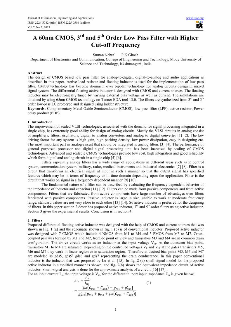
Proposed differential floating active inductor was designed with the help of CMOS and current sources that was
shown in Fig. 1 (a) and the schematic shown in fig. 1 (b) is of conventional inductor. Proposed active inductor
was designed with 7 CMOS which include 4 NMOS from M1 to M4 and 3 PMOS from M5 to M7. Cross-
coupled pair was formed by M1 and M2, from dc point of view and transistors M3 and M4 are in common drain
configuration. The above circuit works as an inductor at the input voltage Vin. At the quiescent bias point,
transistors M1 to M4 are saturated. Depending on the controlled voltages Vb and Vbb at the gates transistors M5,
M6 and M7 they work in linear region or in saturation region. Therefore at desired bias point M5, M6 and M7
are modeled as gds5, gds5’ gds6 and gds7 representing the drain conductance. In this paper conventional
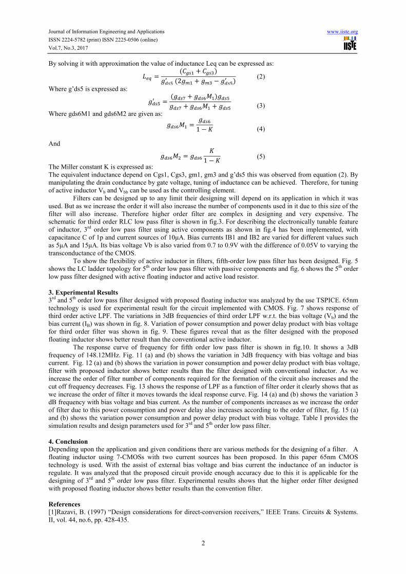
inductor is the inductor that was proposed by Lu et al. [15]. In fig. 2 (a) small-signal model for the proposed
active inductor in simplified manner is shown, and fig. 2(b) shows the equivalent impedance circuit of active
inductor. Small-signal analysis is done for the approximate analysis of a circuit [16] [17].
For an input current Iin, the input voltage is Vin, for the differential port input impedance Zin is given below:
(1)
Journal of Information Engineering and Applications www.iiste.org
ISSN 2224-5782 (print) ISSN 2225-0506 (online)
Vol.7, No.3, 2017
2
By solving it with approximation the value of inductance Leq can be expressed as:
2
Where g’ds5 is expressed as:
!" !"
Where gds6M1 and gds6M2 are given as:
!" !1 $
And
!"% !$
1 $
The Miller constant K is expressed as:
The equivalent inductance depend on Cgs1, Cgs3, gm1, gm3 and g’ds5 this was observed from equation (2). By
manipulating the drain conductance by gate voltage, tuning of inductance can be achieved. Therefore, for tuning
of active inductor Vb and Vbb can be used as the controlling element.
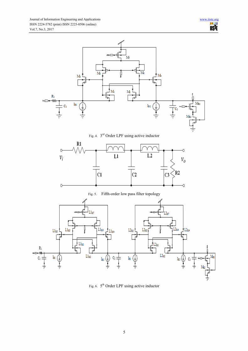
Filters can be designed up to any limit their designing will depend on its application in which it was
used. But as we increase the order it will also increase the number of components used in it due to this size of the
filter will also increase. Therefore higher order filter are complex in designing and very expensive. The
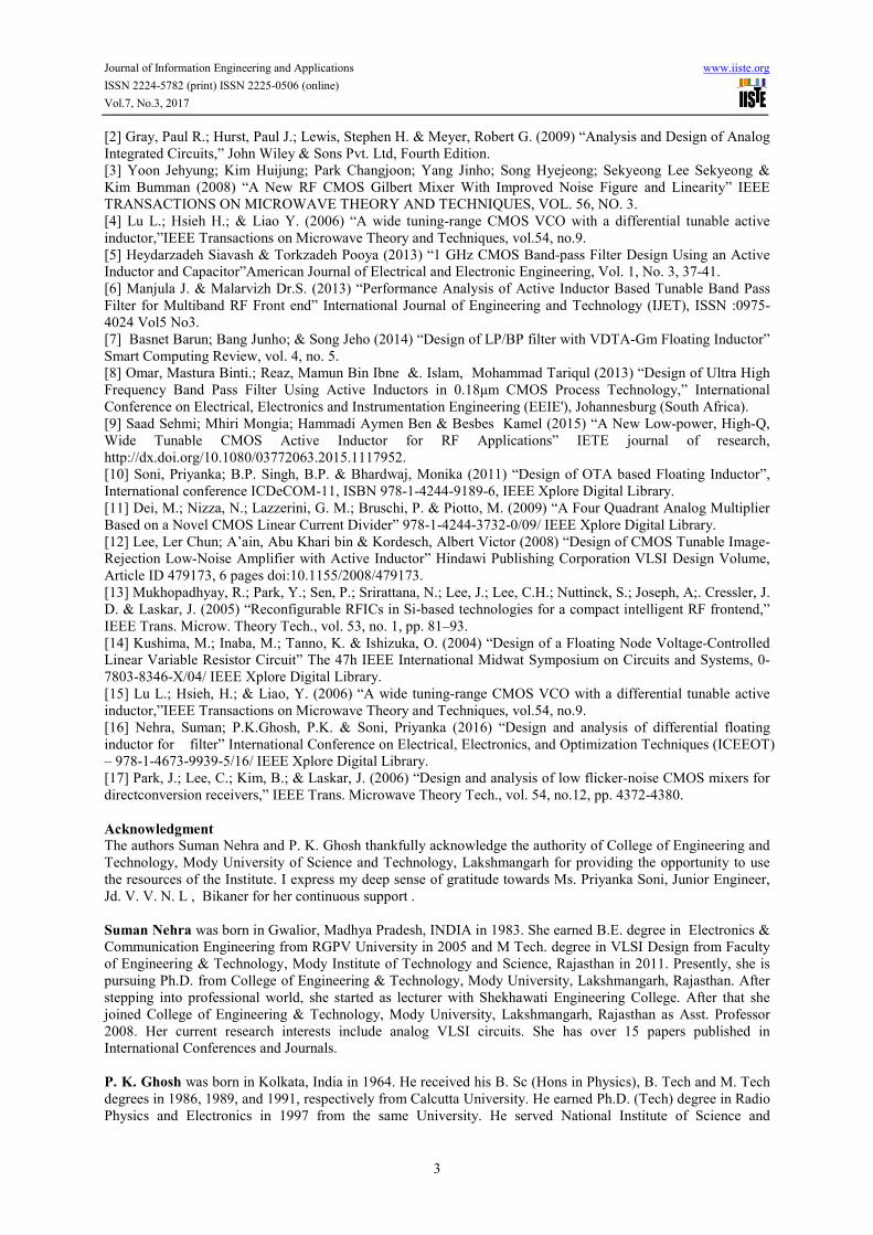
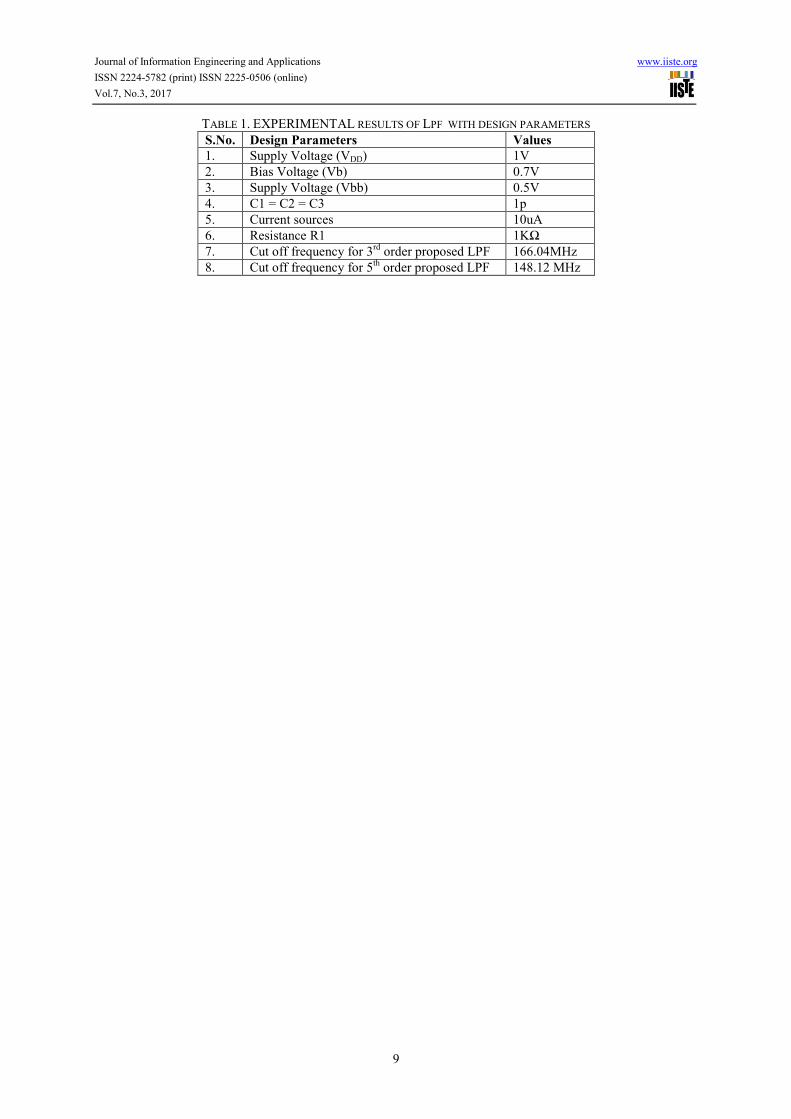
schematic for third order RLC low pass filter is shown in fig.3. For describing the electronically tunable feature
of inductor, 3rd
order low pass filter using active components as shown in fig.4 has been implemented, with
capacitance C of 1p and current sources of 10µA. Bias currents IB1 and IB2 are varied for different values such
as 5µA and 15µA. Its bias voltage Vb is also varied from 0.7 to 0.9V with the difference of 0.05V to varying the
transconductance of the CMOS.
To show the flexibility of active inductor in filters, fifth-order low pass filter has been designed. Fig. 5
shows the LC ladder topology for 5th order low pass filter with passive components and fig. 6 shows the 5
th order
low pass filter designed with active floating inductor and active load resistor.
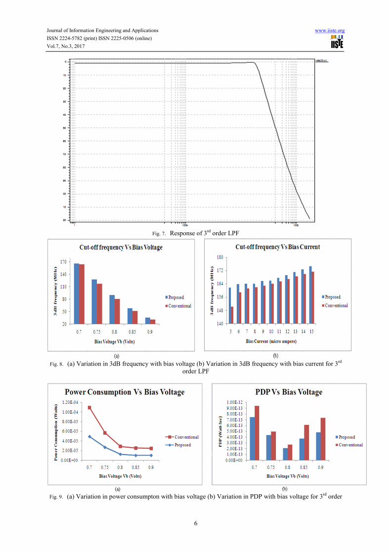
3. Experimental Results
3rd
and 5th order low pass filter designed with proposed floating inductor was analyzed by the use TSPICE. 65nm
technology is used for experimental result for the circuit implemented with CMOS. Fig. 7 shows response of
third order active LPF. The variations in 3dB frequencies of third order LPF w.r.t. the bias voltage (Vb) and the
bias current (IB) was shown in fig. 8. Variation of power consumption and power delay product with bias voltage
for third order filter was shown in fig. 9. These figures reveal that as the filter designed with the proposed
floating inductor shows better result than the conventional active inductor.
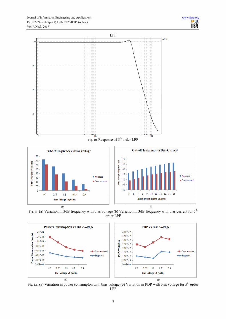
The response curve of frequency for fifth order low pass filter is shown in fig.10. It shows a 3dB
frequency of 148.12MHz. Fig. 11 (a) and (b) shows the variation in 3dB frequency with bias voltage and bias
current. Fig. 12 (a) and (b) shows the variation in power consumption and power delay product with bias voltage,
filter with proposed inductor shows better results than the filter designed with conventional inductor. As we
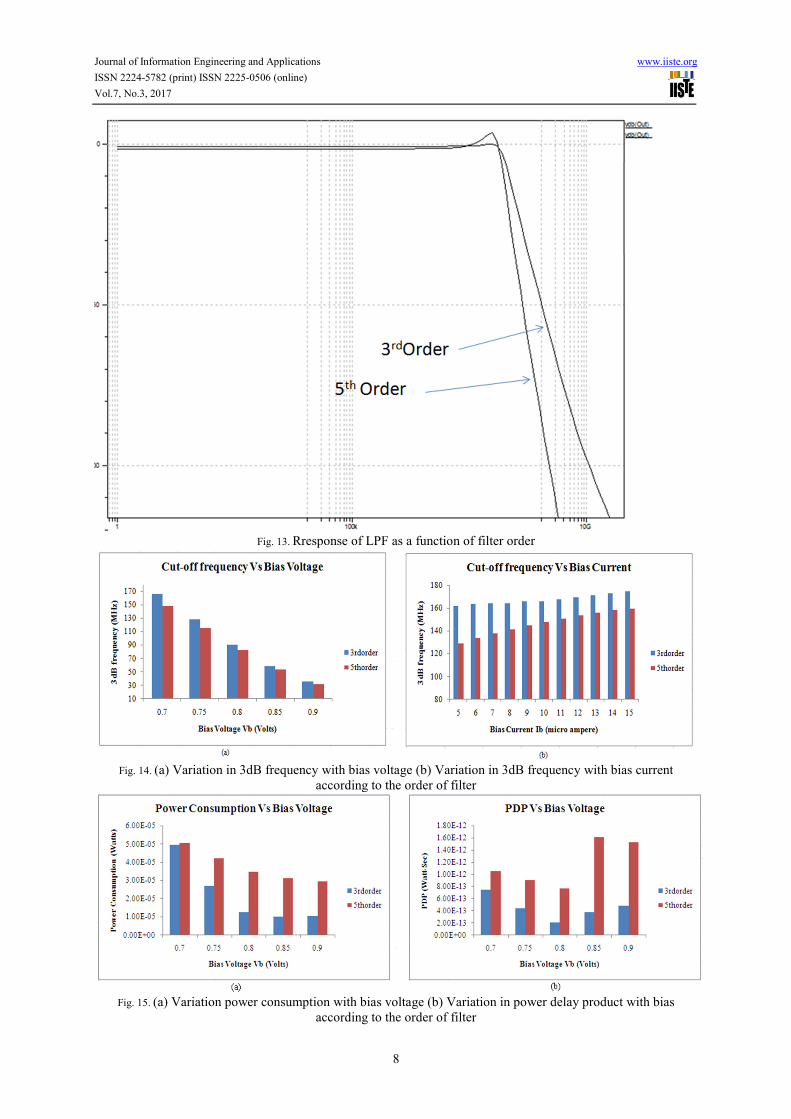
increase the order of filter number of components required for the formation of the circuit also increases and the
cut off frequency decreases. Fig. 13 shows the response of LPF as a function of filter order it clearly shows that as
we increase the order of filter it moves towards the ideal response curve. Fig. 14 (a) and (b) shows the variation 3
dB frequency with bias voltage and bias current. As the number of components increases as we increase the order
of filter due to this power consumption and power delay also increases according to the order of filter, fig. 15 (a)
and (b) shows the variation power consumption and power delay product with bias voltage. Table I provides the
simulation results and design parameters used for 3rd
and 5th
order low pass filter.
4. Conclusion
Depending upon the application and given conditions there are various methods for the designing of a filter. A
floating inductor using 7-CMOSs with two current sources has been proposed. In this paper 65nm CMOS
technology is used. With the assist of external bias voltage and bias current the inductance of an inductor is
regulate. It was analyzed that the proposed circuit provide enough accuracy due to this it is applicable for the
designing of 3rd
and 5th
order low pass filter. Experimental results shows that the higher order filter designed
with proposed floating inductor shows better results than the convention filter.
References
[1]Razavi, B. (1997) “Design considerations for direct-conversion receivers,” IEEE Trans. Circuits & Systems.
II, vol. 44, no.6, pp. 428-435.
(2)
(3)
(4)
(5)
Journal of Information Engineering and Applications www.iiste.org
ISSN 2224-5782 (print) ISSN 2225-0506 (online)
Vol.7, No.3, 2017
3
[2] Gray, Paul R.; Hurst, Paul J.; Lewis, Stephen H. & Meyer, Robert G. (2009) “Analysis and Design of Analog
Integrated Circuits,” John Wiley & Sons Pvt. Ltd, Fourth Edition.
[3] Yoon Jehyung; Kim Huijung; Park Changjoon; Yang Jinho; Song Hyejeong; Sekyeong Lee Sekyeong &
Kim Bumman (2008) “A New RF CMOS Gilbert Mixer With Improved Noise Figure and Linearity” IEEE
TRANSACTIONS ON MICROWAVE THEORY AND TECHNIQUES, VOL. 56, NO. 3.
[4] Lu L.; Hsieh H.; & Liao Y. (2006) “A wide tuning-range CMOS VCO with a differential tunable active
inductor,”IEEE Transactions on Microwave Theory and Techniques, vol.54, no.9.
[5] Heydarzadeh Siavash & Torkzadeh Pooya (2013) “1 GHz CMOS Band-pass Filter Design Using an Active
Inductor and Capacitor”American Journal of Electrical and Electronic Engineering, Vol. 1, No. 3, 37-41.
[6] Manjula J. & Malarvizh Dr.S. (2013) “Performance Analysis of Active Inductor Based Tunable Band Pass
Filter for Multiband RF Front end” International Journal of Engineering and Technology (IJET), ISSN :0975-
4024 Vol5 No3.
[7] Basnet Barun; Bang Junho; & Song Jeho (2014) “Design of LP/BP filter with VDTA-Gm Floating Inductor”
Smart Computing Review, vol. 4, no. 5.
[8] Omar, Mastura Binti.; Reaz, Mamun Bin Ibne &. Islam, Mohammad Tariqul (2013) “Design of Ultra High
Frequency Band Pass Filter Using Active Inductors in 0.18µm CMOS Process Technology,” International
Conference on Electrical, Electronics and Instrumentation Engineering (EEIE'), Johannesburg (South Africa).
[9] Saad Sehmi; Mhiri Mongia; Hammadi Aymen Ben & Besbes Kamel (2015) “A New Low-power, High-Q,
Wide Tunable CMOS Active Inductor for RF Applications” IETE journal of research,
http://dx.doi.org/10.1080/03772063.2015.1117952.
[10] Soni, Priyanka; B.P. Singh, B.P. & Bhardwaj, Monika (2011) “Design of OTA based Floating Inductor”,
International conference ICDeCOM-11, ISBN 978-1-4244-9189-6, IEEE Xplore Digital Library.
[11] Dei, M.; Nizza, N.; Lazzerini, G. M.; Bruschi, P. & Piotto, M. (2009) “A Four Quadrant Analog Multiplier
Based on a Novel CMOS Linear Current Divider” 978-1-4244-3732-0/09/ IEEE Xplore Digital Library.
[12] Lee, Ler Chun; A’ain, Abu Khari bin & Kordesch, Albert Victor (2008) “Design of CMOS Tunable Image-
Rejection Low-Noise Amplifier with Active Inductor” Hindawi Publishing Corporation VLSI Design Volume,
Article ID 479173, 6 pages doi:10.1155/2008/479173.
[13] Mukhopadhyay, R.; Park, Y.; Sen, P.; Srirattana, N.; Lee, J.; Lee, C.H.; Nuttinck, S.; Joseph, A;. Cressler, J.
D. & Laskar, J. (2005) “Reconfigurable RFICs in Si-based technologies for a compact intelligent RF frontend,”
IEEE Trans. Microw. Theory Tech., vol. 53, no. 1, pp. 81–93.
[14] Kushima, M.; Inaba, M.; Tanno, K. & Ishizuka, O. (2004) “Design of a Floating Node Voltage-Controlled
Linear Variable Resistor Circuit” The 47h IEEE International Midwat Symposium on Circuits and Systems, 0-
7803-8346-X/04/ IEEE Xplore Digital Library.
[15] Lu L.; Hsieh, H.; & Liao, Y. (2006) “A wide tuning-range CMOS VCO with a differential tunable active
inductor,”IEEE Transactions on Microwave Theory and Techniques, vol.54, no.9.
[16] Nehra, Suman; P.K.Ghosh, P.K. & Soni, Priyanka (2016) “Design and analysis of differential floating
inductor for filter” International Conference on Electrical, Electronics, and Optimization Techniques (ICEEOT)
– 978-1-4673-9939-5/16/ IEEE Xplore Digital Library.
[17] Park, J.; Lee, C.; Kim, B.; & Laskar, J. (2006) “Design and analysis of low flicker-noise CMOS mixers for
directconversion receivers,” IEEE Trans. Microwave Theory Tech., vol. 54, no.12, pp. 4372-4380.
Acknowledgment
The authors Suman Nehra and P. K. Ghosh thankfully acknowledge the authority of College of Engineering and
Technology, Mody University of Science and Technology, Lakshmangarh for providing the opportunity to use
the resources of the Institute. I express my deep sense of gratitude towards Ms. Priyanka Soni, Junior Engineer,
Jd. V. V. N. L , Bikaner for her continuous support .
Suman Nehra was born in Gwalior, Madhya Pradesh, INDIA in 1983. She earned B.E. degree in Electronics &
Communication Engineering from RGPV University in 2005 and M Tech. degree in VLSI Design from Faculty
of Engineering & Technology, Mody Institute of Technology and Science, Rajasthan in 2011. Presently, she is
pursuing Ph.D. from College of Engineering & Technology, Mody University, Lakshmangarh, Rajasthan. After
stepping into professional world, she started as lecturer with Shekhawati Engineering College. After that she
joined College of Engineering & Technology, Mody University, Lakshmangarh, Rajasthan as Asst. Professor
2008. Her current research interests include analog VLSI circuits. She has over 15 papers published in
International Conferences and Journals.
P. K. Ghosh was born in Kolkata, India in 1964. He received his B. Sc (Hons in Physics), B. Tech and M. Tech
degrees in 1986, 1989, and 1991, respectively from Calcutta University. He earned Ph.D. (Tech) degree in Radio
Physics and Electronics in 1997 from the same University. He served National Institute of Science and
Journal of Information Engineering and Applications www.iiste.org
ISSN 2224-5782 (print) ISSN 2225-0506 (online)
Vol.7, No.3, 2017
4
Technology (Orissa), St. Xavier’s College (Kolkata), Murshidabad College of Engineering and Technology
(West Bengal), R. D. Engineering College (Uttar Pradesh) and Kalyani Government Engineering College (West
Bengal) before he joins Mody University of Science and Technology (Rajasthan). To his credit, he has more than
80 research papers in Journals of repute and conference proceedings. He is a life member of Indian Society for
Technical Education (ISTE), New Delhi. Awarded Young Scientist in the International Workshop on Physics of
Semiconductor Devices (IWPSD-95) held at National Physical Laboratory, New Delhi during December 11-16,
1995 and was awarded a metal plaque. His research interests are in the areas of wireless communications, digital
signal processing, VLSI circuits & devices.
Fig. 1. (a) Proposed active inductor (b) Conventional active inductor
Fig. 2. (a) Proposed active inductor with small signal model (b) Proposed active inductor with equivalent circuit
Fig. 3. Third-order low pass filter topology
Journal of Information Engineering and Applications www.iiste.org
ISSN 2224-5782 (print) ISSN 2225-0506 (online)
Vol.7, No.3, 2017
5
Fig. 4. 3
rd Order LPF using active inductor
Fig. 5. Fifth-order low pass filter topology
Fig. 6. 5
th Order LPF using active inductor
Journal of Information Engineering and Applications www.iiste.org
ISSN 2224-5782 (print) ISSN 2225-0506 (online)
Vol.7, No.3, 2017
6
Fig. 7. Response of 3
rd order LPF
Fig. 8. (a) Variation in 3dB frequency with bias voltage (b) Variation in 3dB frequency with bias current for 3
rd
order LPF
Fig. 9. (a) Variation in power consumpton with bias voltage (b) Variation in PDP with bias voltage for 3
rd order
Journal of Information Engineering and Applications www.iiste.org
ISSN 2224-5782 (print) ISSN 2225-0506 (online)
Vol.7, No.3, 2017
7
LPF
Fig. 10. Response of 5
th order LPF
Fig. 11. (a) Variation in 3dB frequency with bias voltage (b) Variation in 3dB frequency with bias current for 5
th
order LPF
Fig. 12. (a) Variation in power consumpton with bias voltage (b) Variation in PDP with bias voltage for 5
th order
LPF
Journal of Information Engineering and Applications www.iiste.org
ISSN 2224-5782 (print) ISSN 2225-0506 (online)
Vol.7, No.3, 2017
8
Fig. 13. Rresponse of LPF as a function of filter order
Fig. 14. (a) Variation in 3dB frequency with bias voltage (b) Variation in 3dB frequency with bias current
according to the order of filter
Fig. 15. (a) Variation power consumption with bias voltage (b) Variation in power delay product with bias
according to the order of filter
Journal of Information Engineering and Applications www.iiste.org
ISSN 2224-5782 (print) ISSN 2225-0506 (online)
Vol.7, No.3, 2017
9
TABLE 1. EXPERIMENTAL RESULTS OF LPF WITH DESIGN PARAMETERS
S.No. Design Parameters Values
1. Supply Voltage (VDD) 1V
2. Bias Voltage (Vb) 0.7V
3. Supply Voltage (Vbb) 0.5V
4. C1 = C2 = C3 1p
5. Current sources 10uA
6. Resistance R1 1KΩ
7. Cut off frequency for 3rd
order proposed LPF 166.04MHz
8. Cut off frequency for 5th
order proposed LPF 148.12 MHz
Related Documents