1 A 12-Bit 80 MSamples/sec Pipelined SAR ADC Thesis Report By Yasir Mehmood Siddiqui Registration # MS-3-14-59043 Presented to the Faculty of Graduate School of Science and Engineering of PAFKIET, Karachi In partial Fulfillment Of the Requirements For the Degree of Masters of Science in Engineering Advisor: Dr. Syed Arsalan Jawed Associate Professor PAFKIET October 2016

Welcome message from author
This document is posted to help you gain knowledge. Please leave a comment to let me know what you think about it! Share it to your friends and learn new things together.
Transcript
1
A 12-Bit 80 MSamples/sec
Pipelined SAR ADC Thesis Report
By
Yasir Mehmood Siddiqui
Registration # MS-3-14-59043
Presented to the Faculty of Graduate School of Science and Engineering of PAFKIET,
Karachi
In partial Fulfillment
Of the Requirements
For the Degree of
Masters of Science in Engineering
Advisor: Dr. Syed Arsalan Jawed
Associate Professor
PAFKIET
October 2016

2
Acknowledgements
I would like to thank my Advisor Dr. Syed Arsalan Jawed. Without his guidance, support,
help and continued encouragement I would never have been able to complete this thesis. He
has greatly enhanced my understanding of the many concepts of analog circuit design. I am
also really thankful to him for all the patience he has shown to me during all this duration.
I am really proud of my experience as a graduate student at GSSE, KIET. It has been a
wonderful experience thanks to its research focused environment and professors who are
willing to help students achieve their potential. I would specially like to thank Dr. Husain
Parvez, Dr. Muhammad Bilal Kadri and Dr. Najam Muhammad Amin.
I would also like to thank to my former CEO and mentor Syed Khursheed Enam, thanks to
whom I entered the field of analog circuit design. He has been a great motivation and without
him, I would not have been anywhere near the analog circuit design.
It is also my pleasure to thank my dearest friend Waqas Hassan Siddiqui with whom I had
many discussions while designing the ADC for this thesis.
I would never have reached this place without the constant struggle of both my parents and
especially my mother who left no stone unturned in making me push myself harder and to
achieve the best in everything. I would also like to thank my wife who has shown great
patience and has always been there for me with her support.

3
Abstract:
This thesis presents a pipelined SAR ADC for wireless IEEE802.11n standard which requires a
minimum ADC sampling frequency and resolution of 40MHz and 10bits respectively. Higher
sampling frequency and the resolution of the ADC helps increase the Adjacent Channel Rejection of
the complete system, its jammer performance as well as its input sensitivity. This is the reason, a 12
bit 80MSamples/sec ADC has been designed in this thesis. The ADC utilizes a novel architecture in
which sub-ranging is incorporated in a pipelined SAR along with sub binary DACs. Noise is one of
the main constraints while designing a 12-bit ADC. In a conventional SAR design, the comparator
thermal noise has to be less than the quantization noise of the ADC to achieve the desired resolution.
The pipelined architecture relaxes noise requirements of the comparator. An open loop integrator
based gain stage has been incorporated in the architecture with a novel background gain calibration
method to keep gain constant over process and temperature variation. The 80MSamples/sec 12-bit
Pipelined SAR ADC has been designed and simulated in Global Foundry 55nm. The simulation
results of the ADC show an energy efficiency of 11.24 fJ/ conversion-step with a total power
consumption of 3.46mW. The ADC achieves SINAD of 73.5dB and an ENOB of 11.9 bits.

4
Abbreviation:
ADC Analog to Digital Converter
CMOS Complementary Metal-Oxide Semiconductor
SAR Successive Approximation Register
MSPS Mega-Samples Per Second
FOM Figure Of Merit
ENOB Effective Number Of Bits
LSB Least Significant Bit
DNL Differential Non Linearity
INL Integral Non Linearity
SNDR Signal to Noise and Distortion Ratio
DAC Digital to Analog Converter
NMOS N-type Metal Oxide Semiconductor
PMOS P-type Metal Oxide Semiconductor
SNR Signal to Noise Ratio
R/2R Resistor / 2 Resistor
PVT Process Voltage Temperature
OTA Operational Transconductance Amplifier
DLL Delay Locked Loop
SFDR Spurious Free Dynamic Range
DR Dynamic Range
SQNDR Signal to Quantization Noise and Distortion Ratio

5
Contents List of Figures ......................................................................................................................................... 7
List of Tables .......................................................................................................................................... 9
1. Introduction ................................................................................................................................... 10
1.1 Motivation: .................................................................................................................................. 10
1.2 ADC Survey: ............................................................................................................................... 11
1.3 Organization of this Thesis: ........................................................................................................ 12
2. Overview of SAR ADC ................................................................................................................ 13
2.1 Performance Metrics for an ADC ............................................................................................... 13
2.1.1 Resolution of an ADC .......................................................................................................... 13
2.1.2 Quantization Error ............................................................................................................... 13
2.1.3 Differential Non Linearity ................................................................................................... 13
2.1.4 Integral Non Linearity.......................................................................................................... 13
2.1.5 Signal to Noise and Distortion Ratio ................................................................................... 14
2.1.6 Effective Number of Bits ..................................................................................................... 14
2.1.7 Spurious Free Dynamic Range ............................................................................................ 14
2.1.8 Figure of Merit ..................................................................................................................... 14
2.2 SAR ADC Operation .................................................................................................................. 15
2.3 SAR ADC Implementation ......................................................................................................... 16
2.3.1 Sample and Hold Circuit:..................................................................................................... 16
2.3.2 DAC ..................................................................................................................................... 18
2.3.3 Comparator .......................................................................................................................... 22
2.3.4 Digital Logic ........................................................................................................................ 24
2.3 Redundancy in SAR ADC .......................................................................................................... 24
3. Pipelined SAR ADC ..................................................................................................................... 29
3.1 Pipelined SAR ADC ................................................................................................................... 29
3.2 Architecture of the Pipelined SAR ADC: ................................................................................... 30
3.2.1 Number of Pipeline Stages ................................................................................................... 30
3.2.2 Time Distribution ................................................................................................................. 31
3.2.3 Resolution of each Stage ...................................................................................................... 31
3.2.4 Residue Amplifier: ............................................................................................................... 32
3.3 Specifications for Different Blocks ............................................................................................. 33
3.3.1 1st stage SAR Comparator .................................................................................................... 33
3.3.2 Residue Amplifier: ............................................................................................................... 34
3.3.3 2nd
stage SAR Comparator ................................................................................................... 34
3.3.4 Sub ranging using Flash ....................................................................................................... 35
4. CMOS Design of the SAR ADC .................................................................................................. 36
4.1 Input Sample and Hold: .............................................................................................................. 36
4.1.1 Design of the Input Switch .................................................................................................. 37
6
4.1.1.1 Important Issues in the Switch: ......................................................................................... 37
4.1.1.2 Design of the Bootstrapped Switch: ................................................................................. 37
4.2 DAC: ........................................................................................................................................... 38
4.2.1 Top Plate Sampling DAC: ................................................................................................... 38
4.2.2 Design of the 1st stage DAC ................................................................................................. 40
4.2.3 Design of the 2nd
Stage DAC ............................................................................................... 43
4.3 Design of the Flash Comparators ................................................................................................ 44
4.3.1 Important Issues in Flash Comparator: ................................................................................ 44
4.3.2 Circuit for the Flash Comparator: ........................................................................................ 44
4.4 SAR Comparator: ........................................................................................................................ 47
4.4.1 Important Issues in Comparator ........................................................................................... 48
4.4.2 Comparator Design .............................................................................................................. 48
4.4.3 Comparator Offset Calibration ............................................................................................ 50
4.5 Reference Buffer ......................................................................................................................... 50
4.5.1 Important Issues in Reference Buffer: ................................................................................. 50
4.5.2 Design of the Reference Buffer: .......................................................................................... 50
4.6 Residue Amplifier: ...................................................................................................................... 51
4.6.1 Gain Calibration ................................................................................................................... 54
4.6.2 Residue Amplifier Offset Calibration .................................................................................. 55
4.7 SAR Digital Logic: ..................................................................................................................... 55
4.7.1 SAR Internal Logic .............................................................................................................. 55
4.7.2 SAR Output Digital Logic ................................................................................................... 56
5. Simulation Results, Relevant Discussions and Deductions .......................................................... 57
5.1 Individual Components Simulations: .......................................................................................... 57
5.1.1 SAR Comparator ................................................................................................................... 57
5.1.2 Residue Amplifier ................................................................................................................. 58
5.1.3 Reference Buffer .................................................................................................................. 59
5.2 Top Level Integrated Simulations ............................................................................................... 59
6. Conclusions, Discussions and Further Directions......................................................................... 64

7
List of Figures
FIGURE 1.1 BLOCK DIAGRAM IEEE802.11 A/B/G/N ................................................................... 11
FIGURE 1.2 FOM FOR SAR ADCS, HIGHLIGHTING THE TARGETED FOM AND
RESOLUTION ............................................................................................................................. 12
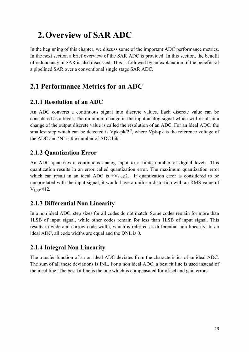
FIGURE 2.1 - IDEAL ADC QUANTIZATION ERROR .................................................................... 14
FIGURE 2.2 A SIMPLE BLOCK DIAGRAM OF THE SAR ADC ................................................... 16
FIGURE 2.3 SAR ADC OPERATION ................................................................................................ 16
FIGURE 2.4 AN OPAMP BASED SAMPLE AND HOLD CIRCUIT ............................................... 17
FIGURE 2.5 A SIMPLE SWITCH AND CAPACITOR BASED SAMPLE AND HOLD CIRCUIT 17
FIGURE 2.6 A CONVENTIONAL BINARY WEIGHTED DAC ARRAY ...................................... 19
FIGURE 2.7 SPLIT CAPACITOR ARRAY DAC .............................................................................. 20
FIGURE 2.8 TOP PLATE SAMPLING DAC .................................................................................... 21
FIGURE 2.9 TIMING DIAGRAM FOR DAC OPERATION AND COMPARATOR OPERATION22
FIGURE 2.10 DYNAMIC COMPARATOR ....................................................................................... 23
FIGURE 2.11 CONVENTION 4-BIT 4 STEP BINARY SEARCH ALGORITHM ........................... 25
FIGURE 2.12 A 4-BIT 4 STEP SAR UNABLE TO RECOVER FROM AN ERROR ....................... 26
FIGURE 2.13 A SUB BINARY SEARCH SAR WHICH RESOLVES 4 BITS IN 5 STEPS ............. 27
FIGURE 2.14 A 4-BIT 5 STEP SAR RECOVERING FROM A WRONG DECISION ..................... 27
FIGURE 2.15 A 4-BIT 5 STEP SAR UNABLE TO RECOVER FROM AN ERROR ....................... 28
FIGURE 3.1 A TWO STAGE PIPELINED SAR ADC ....................................................................... 29
FIGURE 3.2 A 3 STAGE PIPELINED SAR ADC .............................................................................. 30
FIGURE 3.3 TIMING DIAGRAM FOR DIFFERENT PHASES OF THE 1ST STAGE SAR........... 31
FIGURE 3.4 TIMING DIAGRAM WITH THE FLASH ADC INCORPORATED ............................ 32
FIGURE 3.5 FLASH SAR ADC .......................................................................................................... 33
FIGURE 4.1 BLOCK DIAGRAM OF THE SAR ADAC .................................................................... 36
FIGURE 4.2 BOOTSTRAPPED SWITCH ......................................................................................... 38
FIGURE 4.3 TOP PLATE SAMPLING DAC ..................................................................................... 39
FIGURE 4.4 FLOW DIAGRAM OF SAR SET AND UP ALGORITHM .......................................... 40
FIGURE 4.5 1ST STAGE DAC ........................................................................................................... 40
FIGURE 4.6 WAVEFORM OF CONVENTIONAL SWITCHING (TOP) AND SET AND UP SAR
SWITCHING (BOTTOM) ............................................................................................................ 41
FIGURE 4.7 2ND STAGE DAC .......................................................................................................... 43
FIGURE 4.8 FLASH COMPARATOR CIRCUIT ............................................................................... 46
FIGURE 4.9 FLASH COMPARATOR TIMING ................................................................................ 47
FIGURE 4.10 CIRCUIT DIAGRAM OF THE SAR COMPARATOR ............................................... 49
FIGURE 4.11 SCHEMATIC OF THE REFERENCE BUFFER ......................................................... 52
FIGURE 4.12 SCHEMATIC OF THE RESIDUE AMPLIFIER ......................................................... 54

8
FIGURE 5.1 COMPARATOR OUTPUT WITH RISING INPUT VOLTAGE .................................. 57
FIGURE 5.2 COMPARATOR OUTPUT WITH FALLING INPUT VOLTAGE ............................... 58
FIGURE 5.3 INPUT REFERRED NOISE OF SAR COMPARATOR ................................................ 58
FIGURE 5.4 IM3 OF RESIDUE AMPLIFIER .................................................................................... 59
FIGURE 5.5 INPUT REFERRED NOISE OF RESIDUE AMPLIFIER ............................................. 60
FIGURE 5.6 GAIN AND PHASE PLOT OF THE REFERENCE BUFFER ...................................... 60
FIGURE 5.7 ADC OUTPUT, INL AND DNL .................................................................................... 61
FIGURE 5.8 CURRENT CONSUMPTION OF THE ADC ................................................................ 61
FIGURE 5.9 FFT SPECTRUM AT 80MHZ ........................................................................................ 62
FIGURE 5.10 DR ACHIEVED BY THE ADC ................................................................................... 62

9
List of Tables
Table 4-1 Performance Of The Flash Comparator ................................................................................ 47
Table 4-2 Performance Of The Sar Comparator ................................................................................... 49
Table 4-3 Reference Buffer Performance ............................................................................................. 52
Table 4-4 Performance Of Residue Amplifier ...................................................................................... 53
Table 5-1 Performance Results Of The Adc ......................................................................................... 63
Table 5-2 Comparison Table ................................................................................................................ 63

10
1. Introduction
A low power, medium resolution (8-12 bits) and medium sampling rate (KHz – MHz) ADC
is an essential building block of almost all battery powered applications.
The function of an ADC is to convert a continuous time signal with infinite possible states to
a discrete time signal which can only take a limited number of states. The limited number of
states or levels results in quantization error [1] which limits the SNR of a Nyquist rate ADC
to a certain value depending on its resolution.
In addition to resolution, the other important specification for any ADC is its sampling rate or
sampling frequency. This specification is dictated by the sampling theorem [2] which shows
that proper sampling of an analog signal requires sampling frequency to be more than twice
all other frequencies in the analog signal.
The specifications for an ADC depend on the application in which it is being used. Certain
applications require a very high resolution but a relatively slower sampling rate while others
require a very high sampling rate along with medium resolution. The ADC described in this
thesis is for a wireless LAN application. Motivation for this thesis is discussed in the next
section which is followed by a survey of literature to identify a suitable ADC architecture.
The literature survey is followed by the thesis structure.
1.1 Motivation:
A low power ADC with 10-12 bits resolution and 40-80MSamples/sec is a requirement for
IEEE802.11a/b/g/n standard. The goal of this thesis is to propose a low power ADC for such
a wireless receiver. Figure 1.1 shows the block diagram of the IEEE802.11 a/b/g/n standard
transceiver. Research is still ongoing in ADC design to increase power efficiency of the
ADC, thus reducing its power consumption. Reducing power consumption of the ADC
allows reduction in the overall power consumption of the receiver block because ADC is one
of the major power consuming blocks in the receiver. This is especially important to ensure
longer battery life of the transceiver in battery powered applications.
As CMOS technology is scaling to lower channel length transistors, Drain Induced Barrier
Lowering has reduced the intrinsic gain of the transistor. This reduction in MOS intrinsic
gain makes it difficult to realize architectures which use high gain amplifiers to design
operational amplifiers. Research is ongoing to find out architectures which can suitably work
for such short channel length CMOS technology.

11
Figure 1.1 Block Diagram IEEE802.11 a/b/g/n
The following steps have been performed in the thesis to design the ADC which fulfills the
identified requirements:
Choice of ADC architecture
Design Specifications of Important Blocks
Circuit design of the ADC
Design Verification
1.2 ADC Survey:
The scaling CMOS technology has resulted in lower intrinsic gain of short channel devices
making it difficult to design high gain amplifiers for op-amps. Thus, the pipelined flash
ADCs have suffered because they require a number of amplifiers to provide gain to the
residue between cascaded stages. On the other hand SAR ADCs have benefited from the
scaling of CMOS technology because they do not require any gain stage or amplifier. SAR
ADCs only require a comparator whose response time gets improved with scaling technology
and an accurate DAC. The settling of DAC is also helped as CMOS technology gets scaled.
12
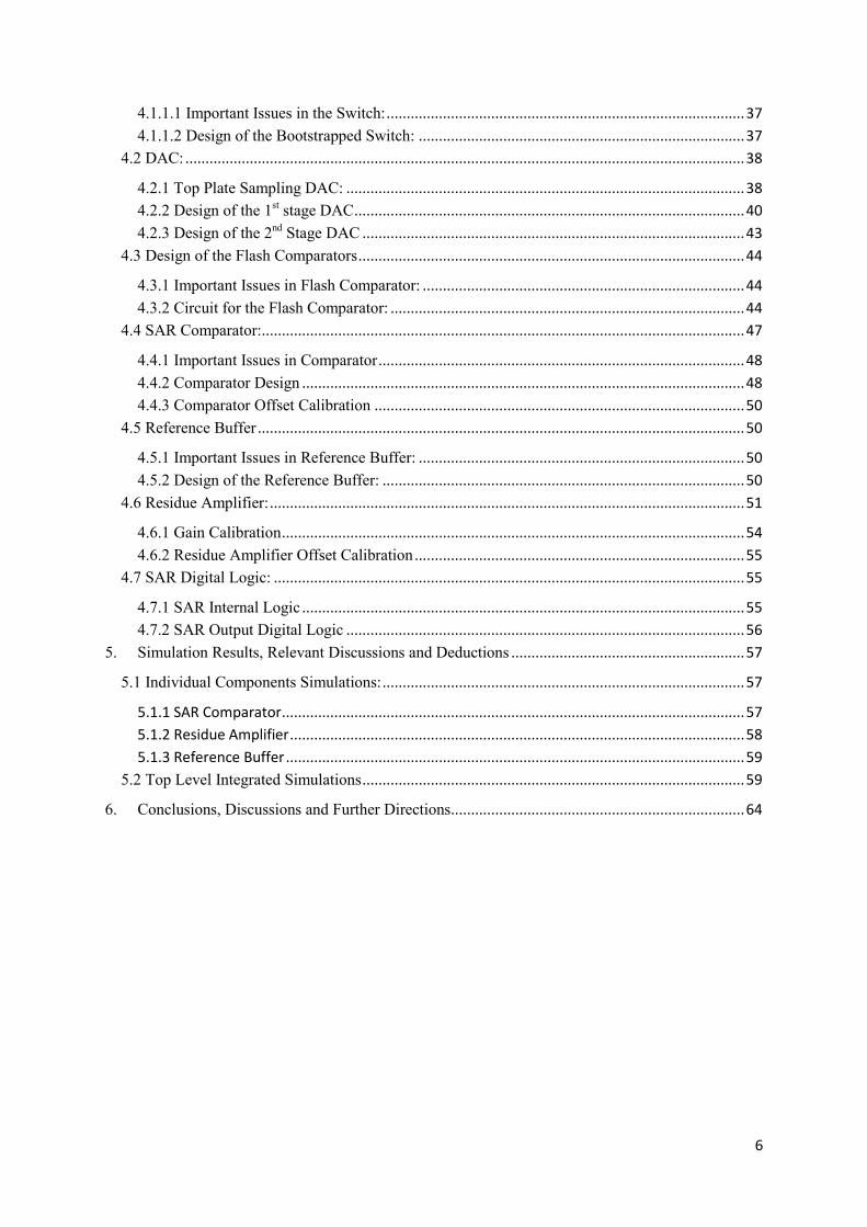
This is the reason, in the past few years SAR ADCs have been the ones with the best energy
efficiency among those reported in the literature. However, it is still difficult to get more than
10 bits with a conventional SAR as most of the papers with high energy efficiency have a
resolution of around 10 bits [3], [4], [5], [6], [7]. The ADCs with the best energy efficiency
[8], [9] are mostly for lower sampling rates and for a resolution of around or less than 10 bits.
[10], [11] and [12] proposed low power pipelined SAR ADCs which helped in achieving high
resolution and a high sampling rate.
Figure 1.2 FOM for SAR ADCs, highlighting the targeted FOM and resolution
1.3 Organization of this Thesis:
In Chapter 2, the basics of a SAR ADC are discussed. In chapter 3, the important blocks of
the pipelined SAR ADC are discussed while chapter 4 discusses the design of each of the
different blocks in the pipelined SAR ADC. The different calibrations employed in the ADC
are also discussed with each block in this chapter. In Chapter 5, results are discussed while
chapter 6 concludes the thesis.
[3],2010,100MSPS
[4],2013,30MSPS
[6],2015,220MSPS
[7],2015,1.1MSPS
[10],2015,160MSPS
[11],2014,80MSPS
[12],2012,250MSPS
[18],2010,50MSPS
[25],2013,150MSPS
[27],2009,50MSPS
[29],2014,50MSPS
[30],2015,20MSPS
[31],2014,40MSPS
[32],2014,100MSPS
[33],2015,5MSPS
0
10
20
30
40
50
60
70
80
90
8.5 9.5 10.5 11.5 12.5 13.5
FOM
= P
/(Fs
*2^
ENO
B)
Resolution (bits)
Targeted
FOM
13
2. Overview of SAR ADC
In the beginning of this chapter, we discuss some of the important ADC performance metrics.
In the next section a brief overview of the SAR ADC is provided. In this section, the benefit
of redundancy in SAR is also discussed. This is followed by an explanation of the benefits of
a pipelined SAR over a conventional single stage SAR ADC.
2.1 Performance Metrics for an ADC
2.1.1 Resolution of an ADC
An ADC converts a continuous signal into discrete values. Each discrete value can be
considered as a level. The minimum change in the input analog signal which will result in a
change of the output discrete value is called the resolution of an ADC. For an ideal ADC, the
smallest step which can be detected is Vpk-pk/2N, where Vpk-pk is the reference voltage of
the ADC and „N‟ is the number of ADC bits.
2.1.2 Quantization Error
An ADC quantizes a continuous analog input to a finite number of digital levels. This
quantization results in an error called quantization error. The maximum quantization error
which can result in an ideal ADC is ±VLSB/2. If quantization error is considered to be
uncorrelated with the input signal, it would have a uniform distortion with an RMS value of
VLSB/√12.
2.1.3 Differential Non Linearity
In a non ideal ADC, step sizes for all codes do not match. Some codes remain for more than
1LSB of input signal, while other codes remain for less than 1LSB of input signal. This
results in wide and narrow code width, which is referred as differential non linearity. In an
ideal ADC, all code widths are equal and the DNL is 0.
2.1.4 Integral Non Linearity
The transfer function of a non ideal ADC deviates from the characteristics of an ideal ADC.
The sum of all these deviations is INL. For a non ideal ADC, a best fit line is used instead of
the ideal line. The best fit line is the one which is compensated for offset and gain errors.
14
Figure 2.1 - Ideal ADC Quantization Error
2.1.5 Signal to Noise and Distortion Ratio
The SNDR for an ADC is the ratio between the input signal and the root mean square sum of
all the other spectral components. The value of the SNDR is dependent on input signal
frequency as well as its amplitude.
2.1.6 Effective Number of Bits
The effective number of bits for an ADC can be calculated from the SNDR value according
to the following formula
𝐸𝑁𝑂𝐵 = (𝑆𝑁𝐷𝑅 − 1.76)/6.02 (Eq. 2.1)
2.1.7 Spurious Free Dynamic Range
The ratio of the input signal to the peak component in the spectrum, whether it is harmonic or
not, is called Spurious Free Dynamic Range.
2.1.8 Figure of Merit
The energy efficiency is the figure of merit used to characterize ADCs. A number of different
metrics have been proposed but the most popular FOM is the following
FoM = P/ (2ENOB
*Fs) (Eq. 2.2)

15
Where,
P is power consumption of the ADC
ENOB is the effective number of bits and
Fs is the sampling frequency
2.2 SAR ADC Operation
SAR ADCs employ a binary search algorithm to convert an analog signal into a digital value.
The ADC compares the input signal with Vref/2 and assigns this value to the MSB bit. The
result of the first comparison determines the direction of the next comparison. In case the first
comparison showed that the input signal is greater than Vref/2, input signal is then compared
with 3Vref/2 otherwise the comparison is made with Vref/4. The result of the comparison is
assigned to the second MSB. The algorithm continues until all the ADC bits are evaluated.
This algorithm enables a SAR ADC to resolve an input signal into an „N‟ bit digital signal in
„N‟ steps where „N‟ is the resolution of the ADC.
Since the algorithm requires a “greater than or smaller than” decision during each step, a high
gain comparator is required in the SAR ADC to compare the input signal with the reference
voltage. In order to generate the reference voltages, a DAC is also required in the SAR ADC.
Since reference voltages are required to be generated according to the decision made by the
comparator, some digital logic is also required. The digital logic required to generate the
appropriate reference voltage are some flip flops and left shift circuitry. A sample and hold
circuit would also be required when SAR algorithm is used to convert an analog signal into a
digital signal.
The sample and hold circuit samples the input signal according to the sampling frequency of
the ADC and holds it during the conversion phase of the ADC. The comparator compares the
sampled input signal with the reference. The high gain of the comparator ensures that the
output of the comparator reaches one of the rails such that its output can be either considered
a „1‟ or a „0‟. The output of the comparator is provided to the DAC through flip flops such
that if the output of the comparator indicates that the input signal is greater than the reference,
the reference signal would increase otherwise the reference signal would decrease. This
ensures a negative feedback around the whole loop and forces the difference between the
input signal and the reference cto become „0‟.

16
I/P Sample & Hold Co
mp
arator
+
-
DAC
SAR Logic
Input
vref
clk
Figure 2.2 A Simple Block Diagram of the SAR ADC
0.1
0.2
0.3
0.4
0.5
0.6
0.7
0.8
0.9
1
vref
D3 = 1 D2 = 1 D1 = 0 D0 = 0
Figure 2.3 SAR ADC operation
2.3 SAR ADC Implementation
A high gain comparator, a DAC, a sample and hold circuit and some digital logic can be used
to design a complete SAR ADC.
2.3.1 Sample and Hold Circuit:
The sample and hold circuit samples the input signal according to the sampling rate of the
ADC. A unity gain buffer with switches can be used as a sample and hold circuit. A simple
implementation of the sample and hold circuit could be just a switch and a capacitor. A
number of different factors influence the design of the switch. Some of these include the
supply voltage of the ADC, ADC‟s input peak to peak voltage and in case of a differential
ADC, its input common mode voltage as well. A simple design could be a single NMOS or

17
PMOS transistor in or a CMOS transmission gate. However, in certain conditions where the
supply voltage of the ADC is low, in order to ensure linearity, boot strapped switches can
also be required.
Vin
Figure 2.4 An OpAmp based Sample and Hold Circuit
InputSampled input
Figure 2.5 A simple Switch and Capacitor Based Sample and Hold Circuit
The size of the input capacitance depends on the kT/C noise requirement of the ADC. Each
ADC has an inherent quantization noise which limits the SNR of the output. In order to
ensure that the output SNR does not degrade below that specific value the thermal noise of
the ADC should be kept smaller than its quantization noise.
√ (KT/C) = Vpk-pk/ (2^N*2√3) (Eq. 2.3)
Where
Vpk-pk is the peak to peak input voltage of the SAR ADC,
N is the number of bits of the ADC
C is the total input sampling capacitor
The switch resistance needs to be kept small enough to ensure that the input signal
completely settles on the capacitor array during the sampling phase. If a normal CMOS
switch is used to provide a small resistance when the supply is also limited, the size of the
switch would be very large and consequently the issues of channel charge injection and clock
feed through would also become significant. Moreover, the switch resistance would vary over
the whole input signal range because the switch‟s over drive would change with the input
18
signal which would affect the linearity of the signal. This is the reason in most low power
designs, a bootstrapped switch used for input sampling because it ensures that the overdrive
of the switch transistor remains constant at “vdd-vth” across the input voltage range. This
also reduces the size of the switch transistor and issues like channel charge injection and
clock feed through are greatly reduced.
2.3.2 DAC
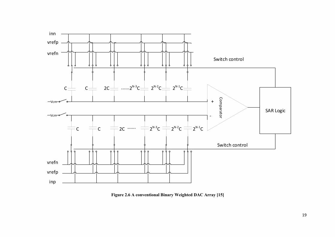
DAC is the most important block in a SAR ADC. A number of different DAC architectures
can be used in the SAR ADC. R/2R ladder DAC, current steering DAC or charge
redistribution DAC. All can be incorporated in a SAR ADC. However, since most other
DACs have certain static consumption apart from the charge redistribution DAC, it is
preferred in a SAR ADC.
There are a number of different architectures of capacitor based charge redistribution DACs
which can be employed in a SAR ADC.
A conventional binary weighted capacitor DAC array is shown in the figure 2.6. The
capacitor array is made up of unit capacitors „Cu‟. The MSB capacitor in the array is equal to
2N-1
where N is the resolution of the ADC. A dummy capacitor is also included in the array to
ensure that the total capacitor array size is 2NCu.
The DAC shown incorporates the sample and hold circuit. During the sampling phase, the
bottom plates of all capacitors in the array apart from the dummy capacitor are connected to
the input signal, while the top plate is connected to a common voltage. During the conversion
phase, the top plate is left floating, while the bottom plate of each capacitor is connected to
either “Vref” or ground depending on the previous decisions of the comparator.
19
Co
mp
arator
+
-
2N-1C2N-2C2N-3C .2CCC
Vcm
vrefn
vrefp
inp
C 2C . 2N-3C 2N-2C 2N-1C
Vcm
vrefn
vrefp
inn
SAR Logic
C
Switch control
Switch control
Figure 2.6 A conventional Binary Weighted DAC Array [15]

20
Co
mp
arator
+
-
4CM2CMCM2CLCLCL
Csplit
MSBsLSBs
vrefn
vrefp
vin
vcm
vcmvcm
Figure 2.7 Split Capacitor Array DAC [16]
A split or attenuation capacitor array DAC is shown in figure 2.7. This DAC array
incorporates a series capacitor between two binary weighted capacitor DAC arrays. The
purpose of the split or attenuation capacitor is to decrease the overall size of the DAC array.
For an N-bit resolution DAC, if each DAC array is made up of N/2 capacitor elements, the
total size of the DAC would be 2(N/2+1)
which is much smaller than 2N. The value of the
attenuation capacitor which connects the MSB and the LSB plates can be calculated from the
formula:
Catt = 2(N/2)
/ (2N/2
-1) (Eq. 2.4)
Given that each array has equal N/2 capacitors.
The operation of the split capacitor Array DAC is similar to the conventional binary weighted
capacitor DAC. The split capacitor Array DAC not only reduces the total area occupied by
the DAC, it also decreases its dynamic power consumption because its total capacitor size is
decreased. It also relaxes the settling time of the reference voltage. The problem with this
capacitor array is that the coupling capacitor is not a unit capacitor and thus its matching may
become an issue. Moreover, the parasitic capacitance on the LSB DAC would affect the
overall linearity of the DAC array [17].

21
Co
mp
arator
+
-
2N-2C2N-3C2N-4C .2CCC
vrefn
vrefp
C 2C . 2N-4C 2N-3C 2N-2C
vrefn
vrefp
SAR Logic
C
Switch control
Switch control
inn
inp
Figure 2.8 Top Plate Sampling DAC [18]

22
Figure 2.8 shows a top plate sampling DAC with binary weighted capacitors. In this DAC,
during sampling phase, the top plate of each capacitor in the array is connected to the input
signal, while the bottom plate is connected to ground. During conversion phase, the top plate
is kept floating, while the bottom plate of the different capacitors in the array are connected
to either „vrefp‟ or „vrefn‟ depending on the outputs from the comparator.
DAC settling is an important parameter for the correct operation and performance of the SAR
ADC. DAC settling depends on the settling of the reference voltages and the time constant
formed by the switch resistance and the unit capacitor (where switch resistance is the
resistance of the switch which connects the reference voltage to the bottom plate of a unit
capacitor). The worst case settling time of the DAC happens when the MSB capacitor is
switched, as this requires the maximum charge from the reference voltage.
For an N bit resolution ADC, having a sampling frequency of Fs, the time period for a single
cycle of the ADC would be
T = 1/ (N*Fs) (Eq. 2.5)
Sampling Clock
Sampling Time Conversion Time
DAC settling Time Comparator Resolution
Figure 2.9 Timing Diagram for DAC operation and Comparator Operation
Two steps are performed in this single high frequency cycle of the SAR ADC. One is DAC
settling, while the other is comparator operation. For proper SAR ADC operation, it is
required that the DAC voltage is settled up to the required resolution before the comparator
starts its operation. Otherwise the ADC output would have errors.
2.3.3 Comparator
The comparator in a SAR ADC should have a resolution such that it can resolve LSB/2 of the
SAR ADC. Moreover, the noise of the comparator should also be less than LSB/2 of the SAR
ADC while keeping the current consumption in an acceptable range.

23
A number of different architectures can be used to design a comparator for SAR ADC.
Generally, comparators can be distributed in two sub classes, static comparators which
require some DC biasing current for their operation and dynamic comparators which operate
without requiring any DC bias. Mostly, dynamic comparators are preferred in SAR ADCs.
As discussed in the previous section, a single cycle of the SAR ADC operation is divided
between the DAC settling time and the comparator operation. This implies that for the
portion of time, DAC is settling the comparator would not be operational. This is the reason,
a fully dynamic comparator is better suited to the SAR operation because it does not consume
any DC bias [19], [20], [21]. This means that the comparator does not consume any power
while the DAC is settling which reduces power consumption. It also ensures that more power
can be consumed while comparator is in operation thus allowing for consuming current to
reduce input noise of the comparator.
While dynamic comparator does reduce the power consumption of the ADC, it also poses the
problem of kick-back noise because of its dynamic nature. Kick-back noise is the disturbance
of the input voltages of the comparator because of large voltage swings on the internal nodes
of the comparator. These large voltage swings appear at the internal nodes of the comparator
because of the switching action of the comparator. These large internal node voltages couple
to the input node of the comparator through parasitic capacitances. The kick back noise issue
is critical in SAR ADC because the comparator input comes from the DAC which is a critical
node for the overall operation of the ADC. In order to reduce kick back noise, normally a pre
amplifier is added before the dynamic comparator to reduce kick-back to the input nodes.
However, such a pre amplifier consumes dc power and increases the overall power
consumption of the comparator.
M3
inp inn
vss12
vdd12M4 M5
clk
M8 M9
M1
M6
M2
M7
M11M12
M10 M13
outpoutn
Figure 2.10 Dynamic Comparator
24
2.3.4 Digital Logic
Each decision of the comparator needs to be stored to generate the required reference voltage
for the comparator. Moreover, all bits need to be stored to ensure that all the output bits are
available at the end of the conversion phase. In addition to storing the decisions of the
comparator, some additional logic is also needed to provide the required code to the DAC.
A SAR ADC operating at a sampling frequency of Fs requires internal clocks of frequency of
N.Fs. This high frequency clock can be provided as input to the SAR ADC so that internal
clocks can be generated through synchronous logic.
Asynchronous logic can also be used to generate the high frequency internal clocks from the
input sampling clock using delay elements. In an asynchronous design, the input frequency of
the SAR ADC is no more than its sampling frequency as the high frequency clocks are
generated internal through the delay logic. Thus asynchronous design does not have high
clock frequency paths, thus reducing the power consumption of the digital logic.
2.3 Redundancy in SAR ADC
In a normal SAR ADC operation, an error occurs when the comparator is unable to correctly
resolve a difference at its input greater than the resolution of the ADC. The three main causes
of such an error are comparator resolution, capacitor mismatch and reference settling.
For a SAR ADC to provide a certain resolution, its comparator must have a better resolution
otherwise the ADC performance would be greatly compromised. Hence, there is no way a
SAR ADC can perform properly if the comparator makes an error. However, errors due to
reference settling can be accounted for, by building redundancy in the SAR ADC design. [22]
shows that redundancy can be used to ensure that reference settling errors do not degrade the
overall performance of the ADC.
Incorporating redundancy in the ADC requires additional conversion steps to be performed
by the SAR. However, redundancy allows for improved sampling frequency by reducing the
settling time requirement of the DAC.
No conversion errors can be tolerated in a conventional binary search SAR because an N bit
conventional binary search SAR ADC can produce only 2N unique codes and the possible
outputs are also 2N which means that there is a one to one correspondence between the input
analog value and the output codes. This one to one correspondence is shown in the Figure
2.12 which shows that once an output value is rejected during the conversion process, it
cannot be reached again [23].
Though Figure 2.12 shows that a conventional binary search SAR cannot correct an error
made during the conversion process, it shows that if an output code can be reached more than
once in a search cycle, it is possible that output codes discarded once due to an error in the
conversion process can be reached again. Output codes can only be reached more than once

25
in a search cycle if the search is sub binary. A sub binary search would require steps more
than N to resolve an analog input to a digital output of N-bits.
A sub binary search would allow the SAR to recover from errors in the conversion process.
However, it appears to be less efficient because to reach the same resolution, a sub binary
SAR would require more steps than the binary search. Thus, it appears that adding
redundancy in a SAR results in a decrease of the sampling frequency of the ADC, which is
not the reality. This is because, when redundancy is incorporated in a SAR, it can now
recover from errors made in the SAR operation due to incomplete settling of the DAC. In the
initial few cycles when MSB capacitors are being switched, the settling time of the reference
buffer could become a bottleneck in sampling frequency for a conventional binary search
SAR. However, in a sub binary search SAR which can recover from errors made earlier in the
search cycle, incomplete settling would not become a bottleneck because of its redundancy.
Thus sampling frequency can be increased if the redundancy is added carefully.
Figure 2.11 Convention 4-bit 4 step binary search algorithm

26
Figure 2.12 A 4-bit 4 step SAR unable to recover from an error
However, it is possible that DAC settling is not the dominant cause of reduced sampling
frequency. In some cases, it is possible that the comparator resolution limits the maximum
sampling frequency at which the SAR ADC can operate. In such conditions, adding
redundancy in the SAR would not at all help in increasing sampling frequency. However, in
most cases where an on chip reference is being used, the settling time of the reference is more
critical because in order to get the required settling, higher power consumption is required.
This is where implementing redundancy can ensure that a low power reference buffer can be
utilized to achieve the same SAR ADC operation.
Figure 2.13 shows the sub binary SAR operation when no error is made during the
conversion process. Figure 2.14 shows the operation of the SAR when an error is made in the
first step. The plot shows that the SAR is able to recover from the error thanks to the
redundancy and reaches the correct output. Figure 2.15 shows that not all errors made during
the search operation can be corrected through redundancy. Generally, if a sub binary SAR
takes more extra steps during the search process, it can recover from more errors.

27
Figure 2.13 A sub binary search SAR which resolves 4 bits in 5 steps
Figure 2.14 A 4-bit 5 step SAR recovering from a wrong decision

28
Figure 2.15 A 4-bit 5 step SAR unable to recover from an error

29
3. Pipelined SAR ADC
3.1 Pipelined SAR ADC
1st Stage SAR ADC
Residue Amplifier
2nd Stage SAR ADC
inp
inn
SAR Encoder
and Calibration Logic
N bits
Figure 3.1 A two stage Pipelined SAR ADC
A pipelined SAR ADC is shown in figure 3.1. In a pipelined SAR ADC, the first stage SAR
resolves input signal up to a certain resolution. The residue is intrinsically generated if a
charge redistribution DAC is designed for the SAR ADC. A residue amplifier provides a
certain gain to this residue. The second SAR then resolves the amplified residue and after
post processing a high resolution output can be obtained just like a pipelined ADC. If over
range is correctly implemented as shown in [11] and [24], the first stage SAR would just have
to be accurate up to its resolution and thus the noise specifications for the first stage ADC‟s
comparator is relaxed. This happens because the over range implemented in the pipelined
SAR ADC allows the output generated by the second stage SAR to correct the errors
introduced by the comparator of the first stage. The noise specifications of the second stage
get relaxed thanks to the gain provided by the residue amplifier. Thus, the only noise critical
block in the design of a pipelined SAR ADC is its gain stage. This relaxation of noise
specification for comparator is the reason pipelined SAR ADC is becoming popular in low
power high resolution designs [10], [11], [12].

30
1st Stage SAR ADC
Residue Amplifier
2nd Stage SAR ADC
inp
inn
SAR Encoder
and Calibration Logic
Residue Amplifier
3rd Stage SAR ADC
Figure 3.2 A 3 stage Pipelined SAR ADC
3.2 Architecture of the Pipelined SAR ADC:
3.2.1 Number of Pipeline Stages
The first step in designing a pipelined SAR ADC is to determine the number of pipeline
stages to be used in the ADC. Increasing the number of pipeline would require a higher
number of gain elements which would increase power consumption. The accuracy
requirements for the comparators further down the chain would decrease. However, having
pipeline stages more than 2 would result more in increased power consumption because of
the additional gain element than decreasing the power consumption because of relaxed
specifications for the comparator and reduced capacitor size. Moreover, having even a 3 stage
pipeline for a 12 bit ADC would require each stage to have a resolution of around 4. This
would result in a high peak to peak signal appearing at the input of the 1st gain element which
would complicate the task of designing a linear gain stage. On the other hand, requiring more
bits to be resolved after the 1st stage would impose strict linearity requirements on the 1
st
stage gain element making its realization very difficult.
31
One benefit which can be obtained from using more than 2 pipeline stages is the increased
sampling frequency of the ADC. Since lesser bits are needed to be resolved in each stage
because of the extra pipeline stage, the sampling frequency of the ADC can be increased
while keeping the internal comparator clock at the same frequency. However, this approach
would also reduce the time for the gain elements (residue amplifier) requiring it to have more
bandwidth which would eventually result in increasing its power consumption. This is the
reason, in this design the number of pipeline stages is kept to 2.
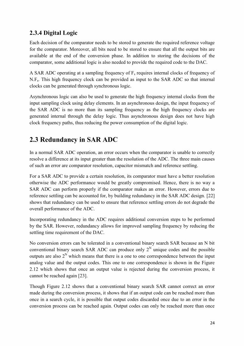
3.2.2 Time Distribution
The total time available to both stages is same. However, the first stage SAR has to perform
three tasks during that time period i.e. sampling, conversion and residue amplification while
the second stage SAR only needs to perform sampling and conversion.
In order to ensure that enough time is available for all three tasks in the first stage SAR, an
additional DAC is used in the 1st stage SAR ADC. In the first cycle, the DAC „1‟ samples the
input. In the second clock cycle, DAC „1‟ enters conversion phase for the first half cycle and
amplification in the second half cycle. In order to maintain sampling frequency, DAC „2‟
samples during the second clock cycle. In the third cycle, the DAC „2‟ would perform
conversion in the first half cycle and amplification in the second half cycle, while DAC „1‟ is
in sampling phase.
Sampling Clock
Sampling ResolutionResidue
AmplificationStage 1 – DAC 1
Sampling Resolution Residue AmplificationStage 1 – DAC 2
Sampling
Sampling ResolutionStage 2 –
DACSampling
Figure 3.3 Timing Diagram for Different Phases of the 1st stage SAR
Timing diagram in figure 3.3 clearly illustrates the distribution of different tasks in different
cycles for both DAC “1” and “2”. The diagram also clearly illustrates that the time during
which the first stage DACs are in residue amplification phase, the 2nd
stage DAC is in
sampling phase. This illustrates that the DAC of 2nd
stage is connected to the first stage
residue amplifier (gain element).
3.2.3 Resolution of each Stage
Section 3.2.2 clearly indicates that the time for 1st SAR conversion is equal to the time
available for conversion to the 2nd
SAR. This ideally means that each SAR should have half
the total resolution of the ADC. This would ensure that each comparator would have the same

32
specification for resolution, conversion time and noise. However, that would mean that the
residue remaining after the first stage would be large.
In order to ensure that the first stage SAR leaves a smaller residue an 8bit 1st stage SAR is
chosen, while the 2nd
SAR is chosen to be 6 bits. In order to ensure that timing requirement
for each comparator is same and for some additional considerations that would be discussed
later, a 3.5 bit Flash ADC is also incorporated in the 1st stage SAR. The flash ADC would
resolve three bits in the first cycle. The 1st stage SAR could then resolve the 6 bits in the 8
cycles. Thus a total of 8 cycles would be required for the 1st stage SAR to resolve 8 bits just
like the second SAR which would require 8 cycles to resolve 6 bits. The incorporation of sub-
ranging Flash ADC in a pipeline SAR ADC is a novel idea.
Figure 3.4 Timing Diagram with the Flash ADC Incorporated
In order to provide redundancy in both 1st stage and 2
nd stage SAR, two extra steps are
provided to both SARs. Thus the 1st stage SAR would resolve 8bits in 8 cycles, while the 2
nd
stage SAR would resolve 6 bits in 8 cycles.
3.2.4 Residue Amplifier:
The amplifier would be required to provide a gain of 16 to the residue left by the 1st stage
SAR ADC. Generally closed loop amplifiers are used to provide amplification in a pipelined
architecture. However, the requirement for a closed loop amplifier is because of two major
reasons. One is to ensure a high linearity of the system, while the other reason is to keep the
gain fairly constant over PVT corners as well as over frequency range.
In our case, we have considerably reduced the input to the residue amplifier by considerably
increasing the resolution of the first stage SAR. This allows open-loop residue amplifier
architecture to be able to provide the required linearity without having to be linearized.
However, the gain of the amplifier would considerably vary over PVT corners. Background
calibration is performed to correct error generated by unequal gain of the gain stage.
Sampling Clock
Sampling Resolution Residue AmplificationStage 1 – DAC 1
Resolution Residue AmplificationStage 1 – DAC 2
Sampling
Flash Conversion
Sampling
Flash Conversion
Flash Conversion
Sampling Resolution SamplingStage 2 –
DAC

33
inp
inn
SAR DAC
3.5 bit Flash ADC
8Binary Bits
SAR
co
mp
ara
tor
1SAR Digital Logic
14Thermometer Bits
Figure 3.5 Flash SAR ADC
The residue remaining at the end of the first stage SAR ADC would depend upon the
resolution of the first stage SAR. If the number of bits resolved after the first stage SAR is
small, then the residue would be high and so would be the linearity requirement from the gain
stage. Such a design would require a very linear amplifier which would be very difficult to
achieve without feedback. Such an amplifier would result in increased current consumption.
In order to alleviate the need of such an amplifier, the first stage SAR should resolve more
than half the required bits so that an open loop amplifier can be used to provide gain to the
residue.
3.3 Specifications for Different Blocks
Since increasing power efficiency of the design is one of the major aims of the design, power
consumption is an important specification for the overall ADC. Since the target is to design
an ADC with a sampling frequency of around 80 MSamples/sec along with a resolution of 12
bits and FOM of less than 10fJ/conv. step, the overall power consumption of the ADC can be
calculated from the FOM equation of the ADC. The power consumption according to the
requirements is
P = 3.2mW
For a Supply voltage of 1.2V, the current consumption should be around
I = 2.73mA

34
Thus the overall current consumption of the ADC should be around 2.75mA.
3.3.1 1st stage SAR Comparator
Since the first stage SAR is supposed to resolve 8 bits, the resolution of the 1st stage SAR
comparator can be given by
LSB = Vpk-pk /2^8 (Eq. 3.1)
Where
Vpk-pk is the input peak to peak voltage of the ADC and it is set to be „1V‟
Thus, the comparator of the 1st stage SAR should be able to resolve at least Vpk-pk/2^9 while
having an input referred noise of less than Vpk-pk/2^9.
3.3.2 Residue Amplifier:
In a pipelined flash architecture, the gain provided after a particular stage is equal to the
number of bits resolved in that stage. Since, 8 bits are being resolved in the first stage a gain
of 256 or 128 would be required from the reside amplifier which would be very difficult to
achieve. This is the reason, the residue amplifier is supposed to provide a gain of 16.
The output of the residue amplifier which is equal to the input of the second stage would be
equal to
Vin_stage2 = Vres_stage1 * 16 (Eq. 3.2)
Where,
Vres_stage1 is the residue left after the first stage. In case, stage 1 is considered to be an ideal
ADC, the residue would be Vpk-pk/2^8. However, in our case, it is taken to be Vpk-pk/2^6.
Since, the 2nd
stage ADC is supposed to resolve 6 bits in order to provide over range and
error correction, the linearity requirement of the residue amplifier is 40dB.
The input referred noise of the residue amplifier should be less than the quantization noise of
the ADC, which is around 70uV.
3.3.3 2nd
stage SAR Comparator
In order to design the second stage SAR with over range, the second stage SAR is designed to
resolve 6 bits. The input of the second stage SAR from Eq. 3.2 is „Vpk-pk/2^6*16‟ which
comes out to be Vpk-pk/4. Thus the input peak to peak voltage of the second stage SAR is 4
times less than the input peak to peak voltage of the 1st stage SAR. The LSB for stage 2
comparator is given by
LSB_stage2 = Vpk-pk/(4*2^6).
35
LSB_stage2 = Vpk-pk/2^8
Thus, the second stage SAR comparator would have to resolve „Vpk-pk/2^9‟ with an input
noise less than „Vpk-pk/2^9‟ as well.
3.3.4 Sub ranging using Flash
[25] shows that using a flash ADC to resolve the first few MSBs in a SAR ADC reduces the
overall resolution time of the SAR. Moreover, our analysis in section 3.2.3 also shows that
adding a flash in the first stage SAR ADC would help in reducing the timing requirement of
the comparator in the first stage. Therefore, a 3.5 bit flash is incorporated in the first stage.
In order to design the 3.5 bit flash 14 comparators would be used. The references would be
selected such that the ADC can tolerate and error of around ± Vpk-pk/32. The 3.5 bit flash
generates a thermometer code which is directly fed to the thermometer capacitors of the 1st
stage SAR ADC.
The flash comparators should be able to resolve an input difference of less than Vpk-pk/32
with similar noise and offset requirements.

36
4. CMOS Design of the SAR ADC
In the previous chapter we identified the architecture of the pipelined SAR ADC and have
also identified the specifications of some of the important blocks in the ADC. Now, we are
going to use the specifications identified in the previous chapter to design the individual
blocks separately.
Stage 1 SAR ADC
Switch
Switch
Switch
Switch
+
-
Switch
SwitchDAC 2
Switch
Switch
Flash ADC
inp
inn
14
DAC 1
SAR1 Digital Logic
SAR1 Digital Logic
+
- comparator
Switch
Switch
Switch
Switch
Residue Amplifier
- +
+
-
Switch
SwitchDAC
Switch
Switch
SAR2 Digital Logic
+
-
comparator
SAR Clock Generationclk
Stage 2 SAR ADC
Figure 4.1 Block Diagram of the SAR ADAC
4.1 Input Sample and Hold:
As discussed earlier in Chapter 2, in this thesis a charge redistribution methodology has been
adopted which incorporates the input sample and hold circuit in the DAC. There is no
separate OpAmp or buffer for sample and hold in such a scheme, thus saving power
consumption. The sample and hold network in such a scheme is a simple switch followed by
the capacitor.
The most important part of this network is the input switch. Since, in this design a bottom
plate sampling DAC is being used which would be discussed in section 4.2, a single switch
would connect or disconnect the input of the ADC with the top plate of the DAC. The bottom
37
plate of the DAC capacitor array would be connected to ground while input is being sampled
on the top plate.
4.1.1 Design of the Input Switch
The input sampling switch is important because the time constant of the switch‟s resistance
and the input capacitance of the DAC should be small such that the dominating input settling
is because of the input driver.
4.1.1.1 Important Issues in the Switch:
The input common for the designed ADC is set to be 600mV. The input differential peak to
peak of the ADC is „1V‟. The two facts imply that the voltage at the input of the switch
would move from 850mV to 350mV. Since the supply voltage of the ADC is „1.2V‟, a simple
pass gate can ensure that the input resistance of the switch is small.
For a 1pF input capacitance of the DAC, the input resistance should be less than 100ohms to
ensure that the time constant because of the input switch is smaller than the total time
available for input settling. Such a small resistance would require a very large size of the pass
gate. Such a large pass gate size would result in considerable charge injection and clock feed-
through which can cause non linearity in the design. Moreover, since there would be a large
swing at its input, the resistance of the simple pass gate would vary with the input adding
nonlinearity. In order to reduce the impact of the above mentioned affects, a boot strapped
switch is employed because it can provide low on resistance with a much smaller size,
because the NMOS transistor would have a vgs of almost „vdd‟.
4.1.1.2 Design of the Bootstrapped Switch:
A bootstrapped switch uses clock, two MOS transistors connected in positive feedback and
two capacitors to first generate 2*Vdd voltage. It then uses this voltage to bootstrap the gate
voltage of the switch transistor such that the vgs across the transistor remains equal to „vdd‟
when the switch is supposed to be „ON‟ and 0V when the switch is supposed to be „OFF‟.
The switch control signal should not be very low frequency otherwise the capacitors would
start discharging.

38
vss12
vdd12
M1 M2
C1 C2
M5
M6
M3
C3
M4
clk
M7
M8
M9
M1
0
M11
M12
in out
G
S
Figure 4.2 Bootstrapped Switch [26]
Since, the switch transistor has a vgs of „vdd‟ across it, therefore, a small sized transistor can
achieve a low impedance. This helps to reduce the charge injection of the switch as well as its
clock feed through.
The reference switches which connect the reference voltage to the bottom plate of the DAC
capacitor array do not require to be bootstrapped because the bottom plate node is always
connected to one of the two references and channel charge injection in the bottom plate
would not result in any distortion in the ADC. This is the reason simple NMOS transistors are
used as switch to connect reference voltages to the bottom plate of the DAC capacitor array.
4.2 DAC:
4.2.1 Top Plate Sampling DAC:
In a top plate sampling differential DAC, no charge redistribution needs to be performed to
find the decision for the MSB bit. As soon as the input is sampled on the differential input
plates, the comparator can compare and provide the first decision. So, unlike conventional
SAR which operates on trial and error resulting in lesser efficiency, a top plate sampling
DAC sets the capacitors according to the decisions and is more efficient. Moreover, since the
MSB bit is resolved directly without having to perform any charge redistribution, the number
of unit capacitors is reduced by one half in this approach [27].
A top plate sampling DAC helps reduce power consumption and also occupies a smaller area
by reducing the total capacitor array size by half. In this design a monotonic switching
scheme [18], [25] is used because this scheme requires only one reference voltage along with
ground for proper DAC operation.
39
2(N-1)C 2(N-2)C 2C C C .
input
sample
sampleb
gndvref
SAR Digital Logic
Figure 4.3 Top Plate Sampling DAC
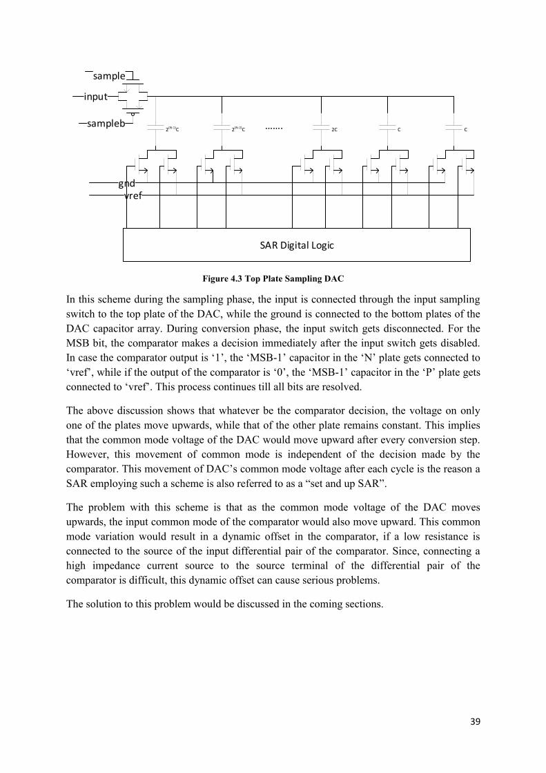
In this scheme during the sampling phase, the input is connected through the input sampling
switch to the top plate of the DAC, while the ground is connected to the bottom plates of the
DAC capacitor array. During conversion phase, the input switch gets disconnected. For the
MSB bit, the comparator makes a decision immediately after the input switch gets disabled.
In case the comparator output is „1‟, the „MSB-1‟ capacitor in the „N‟ plate gets connected to
„vref‟, while if the output of the comparator is „0‟, the „MSB-1‟ capacitor in the „P‟ plate gets
connected to „vref‟. This process continues till all bits are resolved.
The above discussion shows that whatever be the comparator decision, the voltage on only
one of the plates move upwards, while that of the other plate remains constant. This implies
that the common mode voltage of the DAC would move upward after every conversion step.
However, this movement of common mode is independent of the decision made by the
comparator. This movement of DAC‟s common mode voltage after each cycle is the reason a
SAR employing such a scheme is also referred to as a “set and up SAR”.
The problem with this scheme is that as the common mode voltage of the DAC moves
upwards, the input common mode of the comparator would also move upward. This common
mode variation would result in a dynamic offset in the comparator, if a low resistance is
connected to the source of the input differential pair of the comparator. Since, connecting a
high impedance current source to the source terminal of the differential pair of the
comparator is difficult, this dynamic offset can cause serious problems.
The solution to this problem would be discussed in the coming sections.
40
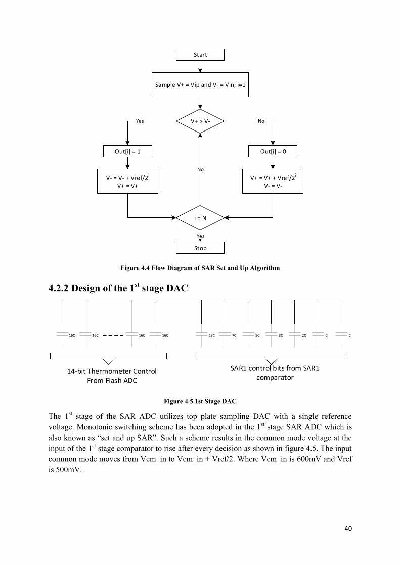
Start
Sample V+ = Vip and V- = Vin; i=1
V+ > V-
Out[i] = 1 Out[i] = 0
V- = V- + Vref/2i
V+ = V+V+ = V+ + Vref/2i
V- = V-
i = N
Stop
Yes No
No
Yes
Figure 4.4 Flow Diagram of SAR Set and Up Algorithm
4.2.2 Design of the 1st stage DAC
Figure 4.5 1st Stage DAC
The 1st stage of the SAR ADC utilizes top plate sampling DAC with a single reference
voltage. Monotonic switching scheme has been adopted in the 1st stage SAR ADC which is
also known as “set and up SAR”. Such a scheme results in the common mode voltage at the
input of the 1st stage comparator to rise after every decision as shown in figure 4.5. The input
common mode moves from Vcm_in to Vcm_in + Vref/2. Where Vcm_in is 600mV and Vref
is 500mV.
13C 2C C C3C5C7C
SAR1 control bits from SAR1 comparator
16C16C16C16C
14-bit Thermometer Control From Flash ADC

41
Vcm
Vinp
Vinm
Sample Phase 1 Phase 2 Phase 3 Phase 4 Phase 5
1 1 0 1 1
Vcm
Vinp
Vinm
Sample Phase 1 Phase 2 Phase 3 Phase 4 Phase 5
1 1 0 1 1
Figure 4.6 Waveform of Conventional switching (top) and set and UP SAR switching (bottom)

42
As discussed in the previous section, this common mode variation at the output of the DAC
and at the input of the comparator can cause a dynamic offset in the comparator which can
result in degraded performance from the SAR ADC. However, solution for this problem has
already been adopted in the previous chapter. That solution is the incorporation of the flash
ADC as a sub-ADC in the complete 1st stage SAR ADC design
The use of flash ADC to resolve the first three bits of the ADC reduces the movement of the
input common mode of the comparator because the first three MSB capacitors are already
decided after the flash ADC has completed its operation. The resultant input common mode
variation reduces by 87.5% to 1/8th
of the original. Thus, the dynamic offset of the
comparator would be less of a problem. Moreover, since sub binary DACs are used in both
stages, the SAR can recover from errors made by the comparator during the conversion cycle
if the final few comparisons are correct. This is the reason dynamic offset of the comparator
is no longer a critical issue.
The size of capacitors chosen for the DAC of the 1st stage SAR should be large enough to
ensure that the KT/C noise is less than the quantization noise of the ADC.
√(KT/C) = Vpk-pk/(2^12*2√3)
(Eq. 4.1)
Where, Vpk-pk is the peak to peak input voltage of the SAR ADC.
From equation 4.1
C = KT*12*2^24/((Vpk-pk)^2)
C = 833fF
Since, the first stage SAR is 8 bits, the Unit Capacitance would be
Cu = C/256
Cu = 3.25fF
Such a small capacitor would not provide the required 12 bit matching in the DAC. This is
the reason a background calibration is incorporated for the first 3 MSBs of the DAC of the
first stage SAR ADC to ensure that the ADC provides the complete 12 bit linearity.
The total capacitance of the 1st stage SAR ADC is set to be 1pF. The LSB of the DAC is
accordingly Cu = 4fF.
In order to ensure that the conversion time for both 1st stage and 2
nd stage SAR is same, the
first three MSBs of the 1st stage are decided using a 3.5 bit flash. The flash operation time is
accommodated in the sampling time of the 1st stage SAR and a separate sample and hold
capacitor is used for the flash ADC.
Since, the first 3 MSBs are obtained from the flash which provides a thermometer code
output, the first 3 MSB capacitors are used as thermometer bits. Each of the 14 outputs

43
coming from the flash switches a capacitor of size 16*Cu which combined account for 7/8 of
the total capacitor size of the DAC. The remaining 6 bits of the first stage are used as sub
binary in order to incorporate redundancy in the first stage SAR.
An extra bit is incorporated in the first stage for background gain calibration. Moreover, this
extra bit also ensures that the residue at the end of the 1st stage is the difference between input
and its 8bit quantized output.
The bottom plate unit capacitor in the DAC array would have to be switched between two
voltages, one is „vref‟ which is set to be 500mV to support a „1V‟ peak to peak input voltage,
the other voltage is ground.
NMOS transistor is used to switch the bottom plate of the unit capacitors to „vref‟ because for
a 1.2V supply and a „vref‟ of 500mV would provide a vgs of more than 700mV to the NMOS
transistor which is more than vdd/2. To switch the DAC‟s bottom plate to ground, another
NMOS transistor is used.
4.2.3 Design of the 2nd
Stage DAC
The second stage DAC contains 6 bits. The architecture used is top plate sampling which is
same as the 1st stage. The 2
nd stage DAC also has the redundancy incorporated in the design
which is the reason it contains sub binary capacitors.
13C 2C C C3C5C7C
SAR2 control bits from SAR2 comparator
Figure 4.7 2nd Stage DAC
Since the 2nd
stage DAC only resolves 6 bits and gain has already been provided in the
Residue Amplifier which provides input to the 2nd
stage SAR ADC, noise requirements are
not that strict in the 2nd
stage SAR. The unit capacitor size chosen in the 2nd
stage SAR is
2.6fF which is the minimum MOM capacitor size available in the technology.
There are two switches to connect bottom plate of the DAC to „vref‟ and „gnd‟. The switch
which connects to both „vref‟ and ground are NMOS.

44
4.3 Design of the Flash Comparators
Each flash comparator needs to be able to resolve 31.25mV. In order to give margin for offset
and noise, each flash comparator is designed to resolve around 10mV in the given time with a
noise of less than 5mV, so enough margin is left for offset of each comparator.
A separate sample and hold capacitor of 400fF is used for the flash comparators because
otherwise it would have affected the voltage on the main sample and hold which is also being
used as the DAC in the first stage SAR ADC. Moreover, in order to ensure that same time is
available for both 1st stage and 2
nd stage SAR conversion cycle, the flash comparators operate
before conversion phase by reducing the sampling time of the 1st stage SAR by a small time
period. The flash comparator operate in„1/(16*Fs)‟, where „Fs‟ is the sampling frequency.
Since for this SAR Fs is 80MHz, the time available for flash comparators is 781.25ps.
4.3.1 Important Issues in Flash Comparator:
Since all flash comparators are going to be operating at the same time, the kickback noise of
the flash stage can become an issue. A separate sample and hold capacitor is placed for the
flash comparators to ensure that the kickback noise does not affect the voltage stored on the
main sampling capacitor. Moreover, two stage comparators are designed for the flash ADC
so that the size of the input pair can be reduced.
The input references of the flash are from 803.125mV to 396.875mV, a rail to rail comparator
is designed for the 3.5 bit Flash ADC.
4.3.2 Circuit for the Flash Comparator:
The comparator has two stages so that the size of the input pair can be reduced. Figure 4.8
shows the schematic diagram of the flash comparator used in the ADC. The first stage is a
rail to rail integrator based circuit. It senses the difference between the input differential
signal and the reference voltages and accordingly charges capacitors at the output of the first
stage.
The gain of the first stage can be given as
G = gm*t/C (Eq. 4.2)
Where,
„gm‟ is the transconductance of the input pair,
„t‟ is the time given to integrate the capacitor, and
C is the size of the capacitor.
The formula shows that in order to increase the gain, either „gm‟ or „t‟ needs to be increased
or „C‟ needs to be decreased. However, if „C‟ is decreased very much both the differential
45
nodes „o1p‟ and „o1n‟ and „o2p‟ and o2n‟ at the output of the first stage would come to
ground potential and though the difference voltage increases it become „0‟ very quickly.
The other way of increasing gain is increasing the integration time. The same phenomenon
happens with increasing the integration time. The final way of increasing the gain is by
increasing „gm‟. Input pair „gm‟ can be increased by increasing by increasing current through
the input pair or its size. If „gm‟ is increased by increasing the size of input pair, kick back
from the flash comparators to their input node increases. If „gm‟ is increased by increasing
current, it would provide more common mode current to the capacitors, and both their nodes
would come to ground quickly.
In order to ensure increased gain from the first stage, the switch transistors „M9‟, „M10‟ and
„M19‟, „M20‟ which become „on‟ while the flash is in reset state are kept „on‟ for a small
duration during the integration time. This ensures that some of the common mode current
flows through the switch transistors and the rest of the common mode current along with the
difference current build voltage across the capacitors which increase the gain of the flash
comparator‟s first stage.

46
Figure 4.8 Flash Comparator Circuit
M1 M2 M3 M4
M5 M6
M7 M8
M9 M10
M11 M12 M13 M14
M15 M16
M17 M18
M19 M20
M21 M22
M23 M24
M25 M26
M27 M28
M29 M30
M31 M32
inp vrefp vrefninn
inp vrefp inn vrefn
enb enb
en en
o1n o1p
o2p o2n
o2p o2n
o1p o1n
outp
vdd12
vss12
clkb clkb
clk clk
clkd clkd
clkbd clkbd
clkd2 clkd2
clkbd2 clkbd2
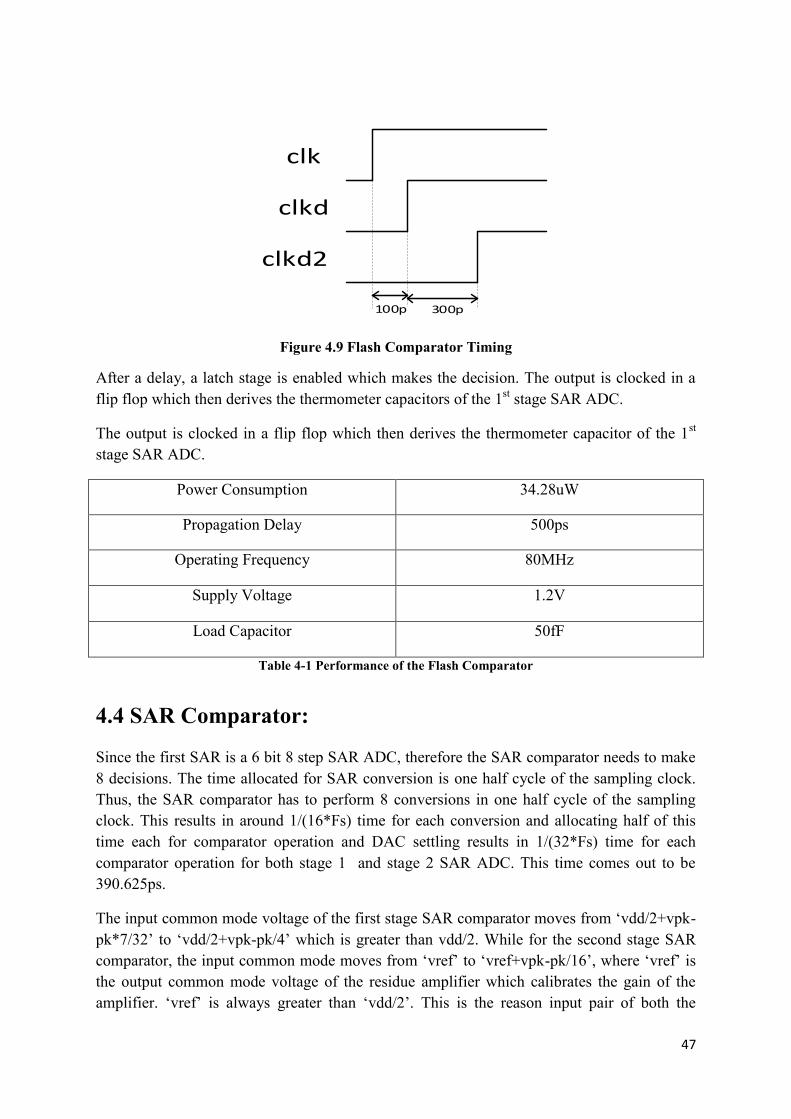
47
Figure 4.9 Flash Comparator Timing
After a delay, a latch stage is enabled which makes the decision. The output is clocked in a
flip flop which then derives the thermometer capacitors of the 1st stage SAR ADC.
The output is clocked in a flip flop which then derives the thermometer capacitor of the 1st
stage SAR ADC.
Power Consumption 34.28uW
Propagation Delay 500ps
Operating Frequency 80MHz
Supply Voltage 1.2V
Load Capacitor 50fF
Table 4-1 Performance of the Flash Comparator
4.4 SAR Comparator:
Since the first SAR is a 6 bit 8 step SAR ADC, therefore the SAR comparator needs to make
8 decisions. The time allocated for SAR conversion is one half cycle of the sampling clock.
Thus, the SAR comparator has to perform 8 conversions in one half cycle of the sampling
clock. This results in around 1/(16*Fs) time for each conversion and allocating half of this
time each for comparator operation and DAC settling results in 1/(32*Fs) time for each
comparator operation for both stage 1 and stage 2 SAR ADC. This time comes out to be
390.625ps.
The input common mode voltage of the first stage SAR comparator moves from „vdd/2+vpk-
pk*7/32‟ to „vdd/2+vpk-pk/4‟ which is greater than vdd/2. While for the second stage SAR
comparator, the input common mode moves from „vref‟ to „vref+vpk-pk/16‟, where „vref‟ is
the output common mode voltage of the residue amplifier which calibrates the gain of the
amplifier. „vref‟ is always greater than „vdd/2‟. This is the reason input pair of both the
clk
clkd
clkd2
100p 300p
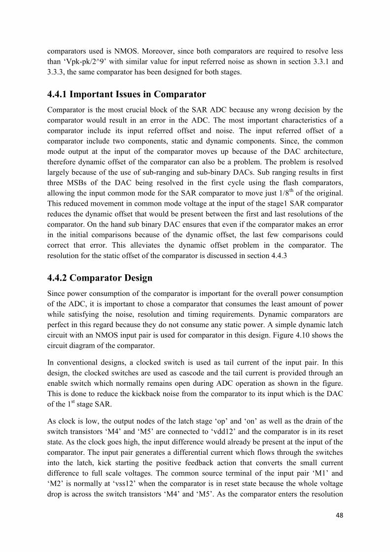
48
comparators used is NMOS. Moreover, since both comparators are required to resolve less
than „Vpk-pk/2^9‟ with similar value for input referred noise as shown in section 3.3.1 and
3.3.3, the same comparator has been designed for both stages.
4.4.1 Important Issues in Comparator
Comparator is the most crucial block of the SAR ADC because any wrong decision by the
comparator would result in an error in the ADC. The most important characteristics of a
comparator include its input referred offset and noise. The input referred offset of a
comparator include two components, static and dynamic components. Since, the common
mode output at the input of the comparator moves up because of the DAC architecture,
therefore dynamic offset of the comparator can also be a problem. The problem is resolved
largely because of the use of sub-ranging and sub-binary DACs. Sub ranging results in first
three MSBs of the DAC being resolved in the first cycle using the flash comparators,
allowing the input common mode for the SAR comparator to move just 1/8th
of the original.
This reduced movement in common mode voltage at the input of the stage1 SAR comparator
reduces the dynamic offset that would be present between the first and last resolutions of the
comparator. On the hand sub binary DAC ensures that even if the comparator makes an error
in the initial comparisons because of the dynamic offset, the last few comparisons could
correct that error. This alleviates the dynamic offset problem in the comparator. The
resolution for the static offset of the comparator is discussed in section 4.4.3
4.4.2 Comparator Design
Since power consumption of the comparator is important for the overall power consumption
of the ADC, it is important to chose a comparator that consumes the least amount of power
while satisfying the noise, resolution and timing requirements. Dynamic comparators are
perfect in this regard because they do not consume any static power. A simple dynamic latch
circuit with an NMOS input pair is used for comparator in this design. Figure 4.10 shows the
circuit diagram of the comparator.
In conventional designs, a clocked switch is used as tail current of the input pair. In this
design, the clocked switches are used as cascode and the tail current is provided through an
enable switch which normally remains open during ADC operation as shown in the figure.
This is done to reduce the kickback noise from the comparator to its input which is the DAC
of the 1st stage SAR.
As clock is low, the output nodes of the latch stage „op‟ and „on‟ as well as the drain of the
switch transistors „M4‟ and „M5‟ are connected to „vdd12‟ and the comparator is in its reset
state. As the clock goes high, the input difference would already be present at the input of the
comparator. The input pair generates a differential current which flows through the switches
into the latch, kick starting the positive feedback action that converts the small current
difference to full scale voltages. The common source terminal of the input pair „M1‟ and
„M2‟ is normally at „vss12‟ when the comparator is in reset state because the whole voltage
drop is across the switch transistors „M4‟ and „M5‟. As the comparator enters the resolution
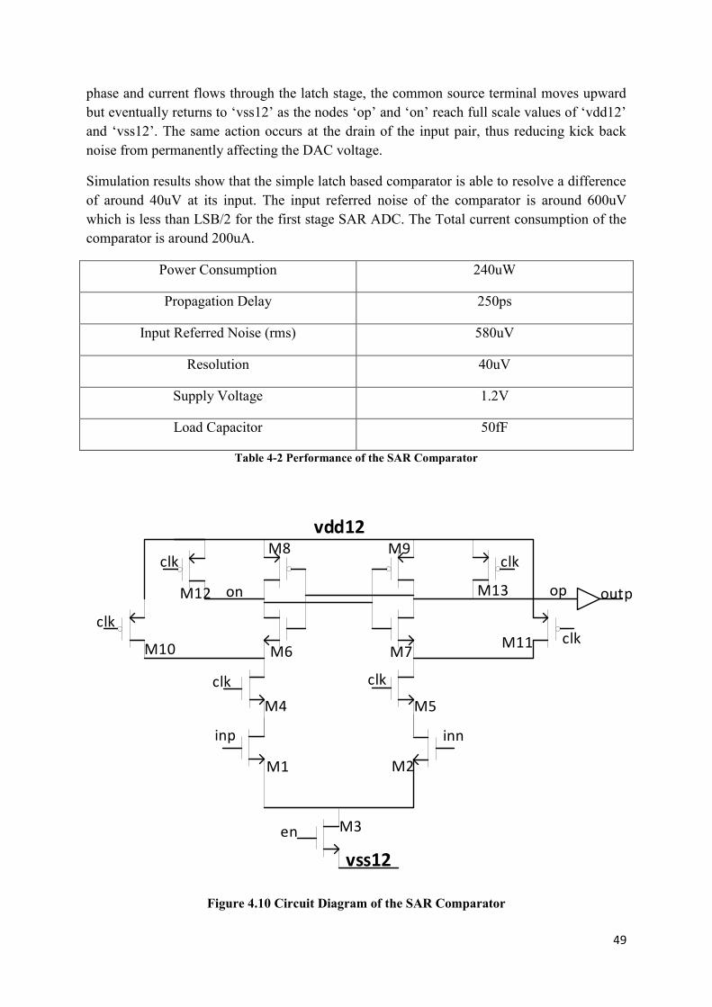
49
phase and current flows through the latch stage, the common source terminal moves upward
but eventually returns to „vss12‟ as the nodes „op‟ and „on‟ reach full scale values of „vdd12‟
and „vss12‟. The same action occurs at the drain of the input pair, thus reducing kick back
noise from permanently affecting the DAC voltage.
Simulation results show that the simple latch based comparator is able to resolve a difference
of around 40uV at its input. The input referred noise of the comparator is around 600uV
which is less than LSB/2 for the first stage SAR ADC. The Total current consumption of the
comparator is around 200uA.
Power Consumption 240uW
Propagation Delay 250ps
Input Referred Noise (rms) 580uV
Resolution 40uV
Supply Voltage 1.2V
Load Capacitor 50fF
Table 4-2 Performance of the SAR Comparator
Figure 4.10 Circuit Diagram of the SAR Comparator
M1 M2
M3
M4 M5
inp inn
en
op
vdd12
vss12
clk clk
clk
clk
M6 M7
M8 M9
M10
on
M11
M13M12 outp
clk
clk

50
4.4.3 Comparator Offset Calibration
The offset of the 1st stage comparator should also be less than the LSB of the SAR ADC,
otherwise the input to the residue amplifier would be large thus it can reduce its input range
and also decrease it linearity. For this purpose an additional differential pair is connected in
parallel with the input pair of the comparator to compensate its offset using foreground
calibration. A 10-bit DAC provides the input to the added differential pair. The 1st stage SAR
Comparator‟s offset is calibrated once the offset of the residue amplifier is calibrated. In
order to calibrate the 1st stage SAR comparator, both its inputs are connected to its input
common mode voltage and its output is connected to the residue amplifier. The outputs of the
residue amplifier are connected to an additional comparator used only for calibration purpose.
A calibration algorithm adjusts the input of the additional differential pair to ensure minimum
offset.
4.5 Reference Buffer
The reference voltage required for the SAR ADC is 500mV, since the DAC used in the ADC
utilizes a “set and up” SAR algorithm.
4.5.1 Important Issues in Reference Buffer:
The reference voltage should be settled to up to 12 bit accuracy during the action of the
residue amplifier.
4.5.2 Design of the Reference Buffer:
The designed reference buffer is an OTA connected in unity gain feedback. Figure 4.11
shows the schematic of the designed OTA. It is a current mirror OTA. The first stage of the
OTA has a PMOS differential pair „M1‟ and „M2‟ and a diode connected NMOS load „M5‟
and „M6‟ reducing the gain of the first stage and also eradicating the need of a miller
capacitor to stabilize the OTA. The second stage is a common source stage with a large
capacitor as the dominant pole. The large capacitor at the output of the buffer ensures that the
reference voltage does not move much.
The overall DC Gain and Unity Gain bandwidth of the OTA are given by the following
equations
A = gm1*β*Rout (Eq. 4.3)
Where,
gm1 is the transconductance of the first stage PMOS differential pair „M1‟ and „M2‟,
β is the current gain between the first stage load NMOS „M6‟ and the second stage NMOS
transistor „M11‟.

51
Rout is the output impedance of the second stage
Funity = gm1*β/C2 (Eq. 4.4)
Where,
C2 is the capacitance at the output of the second stage creating the dominant pole.
In order to increase both the DC Gain and Unity Gain, β and gm1 need to be increased.
However, increasing β beyond a certain value would result in degrading phase margin
because the non dominant pole at the output of the first stage would be pushed back to lower
frequencies, because of miller effect on the Cgd of the second stage NMOS transistor. This is
the reason, in order to increase the DC Gain and Unity Gain of the OTA, gm1 is increased.
However, increase in gm1 requires current consumption. In a conventional current mirror
OTA, the current from the input pair „M1‟ and „M2‟ would have been equal to the current
through „M5‟ and „M6‟. Thus an increase in the input pair‟s current would also increase the
current of „M11‟. However, as shown in figure 4.11, in the designed OTA, current from the
first stage differential pair is diverted from the NMOS load to constant bias transistors „M18‟
and „M20‟. Thus, an increase in the input differential pair increases the „gm‟ of the first stage
but the second stage current can be kept the same, if that increased current goes to the „M18‟
and „M20‟ rather than the load transistors „M5‟ and „M6‟. Thus, for a minor increase in
current, both the DC gain and Unity Gain Frequency of the OTA can be increased.
Simulation results show that the large capacitor of “50pF” connected at the output of the
reference buffer ensures that even during the first cycle when the 1st three MSBs are decided,
the reference voltage does not move more than 5mV. This along with the redundancy ensures
that the reference voltage is accurate enough for the SAR ADC to not make any errors.
4.6 Residue Amplifier:
As has already been discussed in section 3.3.2, the residue amplifier is designed to provide a
gain of at least 16 over all corners, with an expected voltage peak to peak of „Vpk-pk/2^6‟.
This corresponds to an input of ±7.8125mV, and with a gain of 16 and output of 250mV peak
to peak. The stage 2 SAR ADC is required to resolve 6 bits from this 250mV peak to peak
signal.
The Residue Amplifier is therefore supposed to provide linearity of 6 bits at its output after
providing a gain of 16 to a 15.625mV peak to peak input signal while also ensuring that the
noise at its output is less than 2mV.

52
Figure 4.11 Schematic of the Reference Buffer
Power Consumption 720uW
DC Gain 38.4dB
Unity Gain Frequency 90MHz
Phase Margin 66 degrees
Supply Voltage 1.2V
Load Capacitor 50pF
Table 4-3 Reference Buffer Performance
The design of the residue amplifier is based on the design of [11] as shown in figure 4.12. It
consists of an integrator based amplifier. The gain of the amplifier block is given by the
equation
G = gm*T*β/C (Eq. 4.5)
Where,
M1
inn
M2
inp
M3
vcas
M4
vbias
vdd12
M7
vcasn
M5
vcasn
M8
M6
vss12
vcasn
M10
M9
M12
vcasn
M11
M13
M14
vcas
M16
vcas
M15
vcasn
M17
M18
M19
vcasn
M20
vbiasn
out
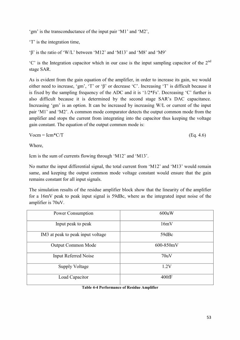
53
„gm‟ is the transconductance of the input pair „M1‟ and „M2‟,
„T‟ is the integration time,
„β‟ is the ratio of „W/L‟ between „M12‟ and „M13‟ and „M8‟ and „M9‟
„C‟ is the Integration capacitor which in our case is the input sampling capacitor of the 2nd
stage SAR.
As is evident from the gain equation of the amplifier, in order to increase its gain, we would
either need to increase, „gm‟, „T‟ or „β‟ or decrease „C‟. Increasing „T‟ is difficult because it
is fixed by the sampling frequency of the ADC and it is „1/2*Fs‟. Decreasing „C‟ further is
also difficult because it is determined by the second stage SAR‟s DAC capacitance.
Increasing „gm‟ is an option. It can be increased by increasing W/L or current of the input
pair „M1‟ and „M2‟. A common mode comparator detects the output common mode from the
amplifier and stops the current from integrating into the capacitor thus keeping the voltage
gain constant. The equation of the output common mode is:
Vocm = Icm*C/T (Eq. 4.6)
Where,
Icm is the sum of currents flowing through „M12‟ and „M13‟.
No matter the input differential signal, the total current from „M12‟ and „M13‟ would remain
same, and keeping the output common mode voltage constant would ensure that the gain
remains constant for all input signals.
The simulation results of the residue amplifier block show that the linearity of the amplifier
for a 16mV peak to peak input signal is 59dBc, where as the integrated input noise of the
amplifier is 70uV.
Power Consumption 600uW
Input peak to peak 16mV
IM3 at peak to peak input voltage 59dBc
Output Common Mode 600-850mV
Input Referred Noise 70uV
Supply Voltage 1.2V
Load Capacitor 400fF
Table 4-4 Performance of Residue Amplifier
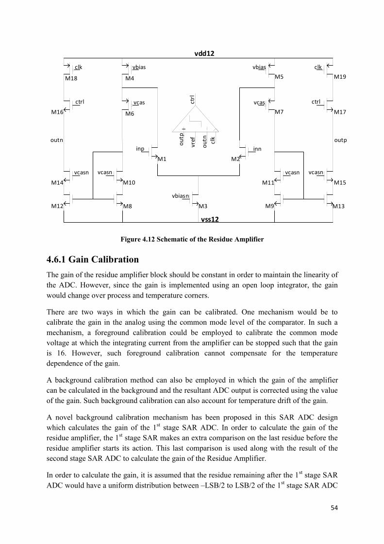
54
Figure 4.12 Schematic of the Residue Amplifier
4.6.1 Gain Calibration
The gain of the residue amplifier block should be constant in order to maintain the linearity of
the ADC. However, since the gain is implemented using an open loop integrator, the gain
would change over process and temperature corners.
There are two ways in which the gain can be calibrated. One mechanism would be to
calibrate the gain in the analog using the common mode level of the comparator. In such a
mechanism, a foreground calibration could be employed to calibrate the common mode
voltage at which the integrating current from the amplifier can be stopped such that the gain
is 16. However, such foreground calibration cannot compensate for the temperature
dependence of the gain.
A background calibration method can also be employed in which the gain of the amplifier
can be calculated in the background and the resultant ADC output is corrected using the value
of the gain. Such background calibration can also account for temperature drift of the gain.
A novel background calibration mechanism has been proposed in this SAR ADC design
which calculates the gain of the 1st stage SAR ADC. In order to calculate the gain of the
residue amplifier, the 1st stage SAR makes an extra comparison on the last residue before the
residue amplifier starts its action. This last comparison is used along with the result of the
second stage SAR ADC to calculate the gain of the Residue Amplifier.
In order to calculate the gain, it is assumed that the residue remaining after the 1st stage SAR
ADC would have a uniform distribution between –LSB/2 to LSB/2 of the 1st stage SAR ADC
inn
M2M1
inp
M3
vbiasn
M4
vbias
M6
vcas
M8
M10
vcasn
M5
vbias
M7
vcas
M9
vcasn
M11
vss12
vdd12
M13
M15
vcasn
M12
vcasn
M14
M17
ctrlctrl
M16
M18
clk
M19
clk
outpoutn
ou
tp
ou
tn
vref clk
ctrl

55
[28]. The final comparison from the 1st stage SAR ADC which compares the final residue
going to the residue amplifier determines whether the remaining is residue is positive or
negative. The output of the second stage SAR is then averaged separately for the positive and
negative results. A difference of the resultant values provides the gain of the residue
amplifier.
4.6.2 Residue Amplifier Offset Calibration
A foreground offset calibration mechanism is used to cancel the offset of the residue
amplifier. During the calibration phase, the inputs of the amplifier block are connected to its
common mode input and the outputs are taken to a comparator used only for calibration
purposes. An additional differential pair is used to cancel the offset of the amplifier block.
The input of the additional differential pair is provided from a 10-bit calibration DAC. A
calibration algorithm would set the value of the calibration DAC such that the offset of the
residue amplifier is minimum.
4.7 SAR Digital Logic:
4.7.1 SAR Internal Logic
The digital logic stores the comparator decisions and switches the reference voltages on the
bottom plate of the DAC to provide the next comparison voltage to the comparator. The input
clock being used by the digital logic is the sampling clock which is 80MHz. The internal high
frequency clocks for comparator operation are being generated inside the ADC using a DLL
(Delay Locked Loop).
The logic for the DAC is such that during sampling phase, bottom plates of all unit
capacitors in the DAC are connected to the ground through an NMOS switch while the top
plate is connected to the input differential voltage through boot strapped switches. As any
DAC enters its conversion phase, decisions from the flash comparators are already stored in
flip flops. The decisions from the flash comparators are used as thermometer code in the SAR
DAC.
If „x‟ outputs from the flash are „1‟, then „x‟ branches of the thermometer capacitor in the „n‟
plate are disconnected from ground and connected to „vref‟ through another NMOS switch.
The remaining ‟14-x‟ branches of the „n‟ plate remain connected to ground. For the „p‟ plate,
‟14-x‟ branches are connected to „vref‟ and disconnected from ground. The remaining „x‟
branches of the „p‟ plate‟s thermometer capacitor remain connected to ground.
The DAC enters conversion phase, the SAR logic generates high frequency clocks for the
comparator operation through DLL, and comparator starts making decisions. If the first
decision of the SAR comparator is „1‟, the bottom plate of the MSB capacitor on the DAC‟s
„n‟ plate is disconnected from ground and connected to „vref‟ while the that of the MSB
capacitor on the DAC‟s „p‟ plate remains connected to ground. While if the first SAR
comparator decision is „0‟ the bottom plate of the MSB capacitor on the DAC‟s „p‟ plate is
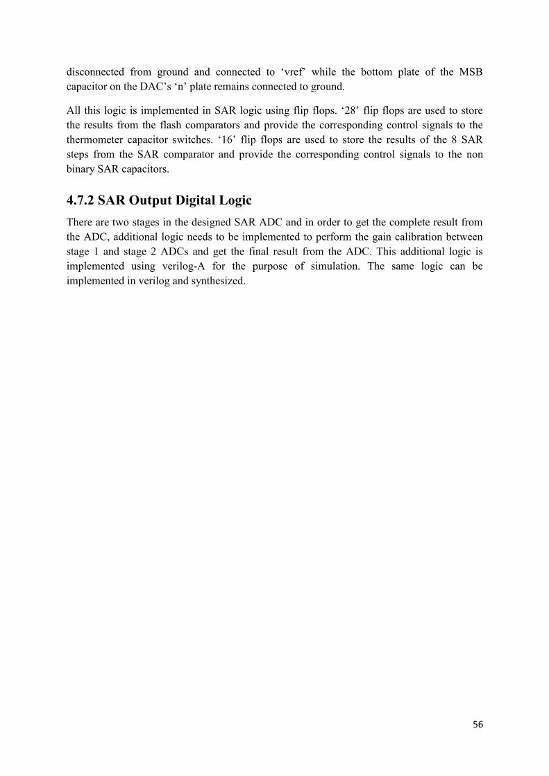
56
disconnected from ground and connected to „vref‟ while the bottom plate of the MSB
capacitor on the DAC‟s „n‟ plate remains connected to ground.
All this logic is implemented in SAR logic using flip flops. „28‟ flip flops are used to store
the results from the flash comparators and provide the corresponding control signals to the
thermometer capacitor switches. „16‟ flip flops are used to store the results of the 8 SAR
steps from the SAR comparator and provide the corresponding control signals to the non
binary SAR capacitors.
4.7.2 SAR Output Digital Logic
There are two stages in the designed SAR ADC and in order to get the complete result from
the ADC, additional logic needs to be implemented to perform the gain calibration between
stage 1 and stage 2 ADCs and get the final result from the ADC. This additional logic is
implemented using verilog-A for the purpose of simulation. The same logic can be
implemented in verilog and synthesized.

57
5. Simulation Results, Relevant Discussions and
Deductions
The ADC has been designed 55nm CMOS technology and the simulation has been performed
in the Virtuoso® Cadence® design environment. Spectre® simulator has been used to
simulate different blocks and the overall ADC.
5.1 Individual Components Simulations:
5.1.1 SAR Comparator
The SAR comparator result for a slow ramp shows that the comparator is able to resolve
input difference of more than 40uV.
Figure 5.1 Comparator output with rising input voltage
As shown in figure 5.1, first a rising input voltage is provided at the comparator‟s input. The
output of the comparator triggers from 0 to 1, when the input becomes greater than 10uV.
Then, as shown in figure 5.2, a falling input voltage is provided to the comparator‟s input.
The comparator output changes from 1 to 0 at around -40uV. Thus, it can be said that the
comparator can resolve input differential voltage of greater than 40uV at its input, with a
dead band from -40uV to 10uV.
Figure 5.3 shows the input referred noise of the comparator from 10 KHz to 320 MHz which
is the Fs/2 of the comparator (since comparator‟s operating clock is 640MHz). The integrated
input referred noise of the comparator is around 580uV which is less than the LSB/2 (2mV)
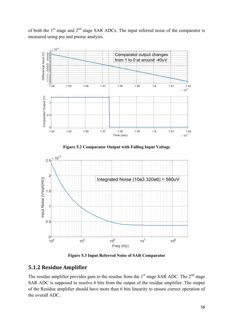
58
of both the 1st stage and 2
nd stage SAR ADCs. The input referred noise of the comparator is
measured using pss and pnoise analysis.
Figure 5.2 Comparator Output with Falling Input Voltage
Figure 5.3 Input Referred Noise of SAR Comparator
5.1.2 Residue Amplifier
The residue amplifier provides gain to the residue from the 1st stage SAR ADC. The 2
nd stage
SAR ADC is supposed to resolve 6 bits from the output of the residue amplifier. The output
of the Residue amplifier should have more than 6 bits linearity to ensure correct operation of
the overall ADC.

59
Figure 5.4 shows that the IM3 of the residue amplifier is around 60dBc for a two tone input
with a peak to peak of 16mV. The IM3 of the residue amplifier is measured at 18MHz and
20MHz.
Figure 5.5 shows the input referred noise of the residue amplifier from 10 KHz to 80 MHz.
The residue amplifier is the most noise critical block in the pipelined SAR ADC and its input
referred noise should be less than the quantization noise of the SAR ADC to ensure that the
noise floor is determined by the quantization noise. Figure 5.5 shows that the integrated input
referred noise of the residue amplifier from 10 KHz to 80 MHz is 70uV which is almost
equal to the quantization noise of the ADC which is also around 70uV. The noise of the
residue amplifier is measured using pss and pnoise analysis
Figure 5.4 IM3 of Residue Amplifier
5.1.3 Reference Buffer
The AC response of the reference buffer is shown in figure 5.6. The plot shows that the DC
Gain of the buffer is around 38dB with a unity gain frequency of around 90MHz and a phase
margin of more than 65o. The reference buffer is simulated with an output load of 50pF. The
results show that the reference buffer is stable.
5.2 Top Level Integrated Simulations:
The results from the simulation are stored in a verilog-A file and post processing is applied to
that data using MATLAB to evaluate the dynamic performance metrics of the ADC. The
transient simulation does not include thermal noise and flicker noise, but as it has already
been shown that the input referred noise of comparator is well below the LSB/2 of the ADCs,
it would not impact the results much.
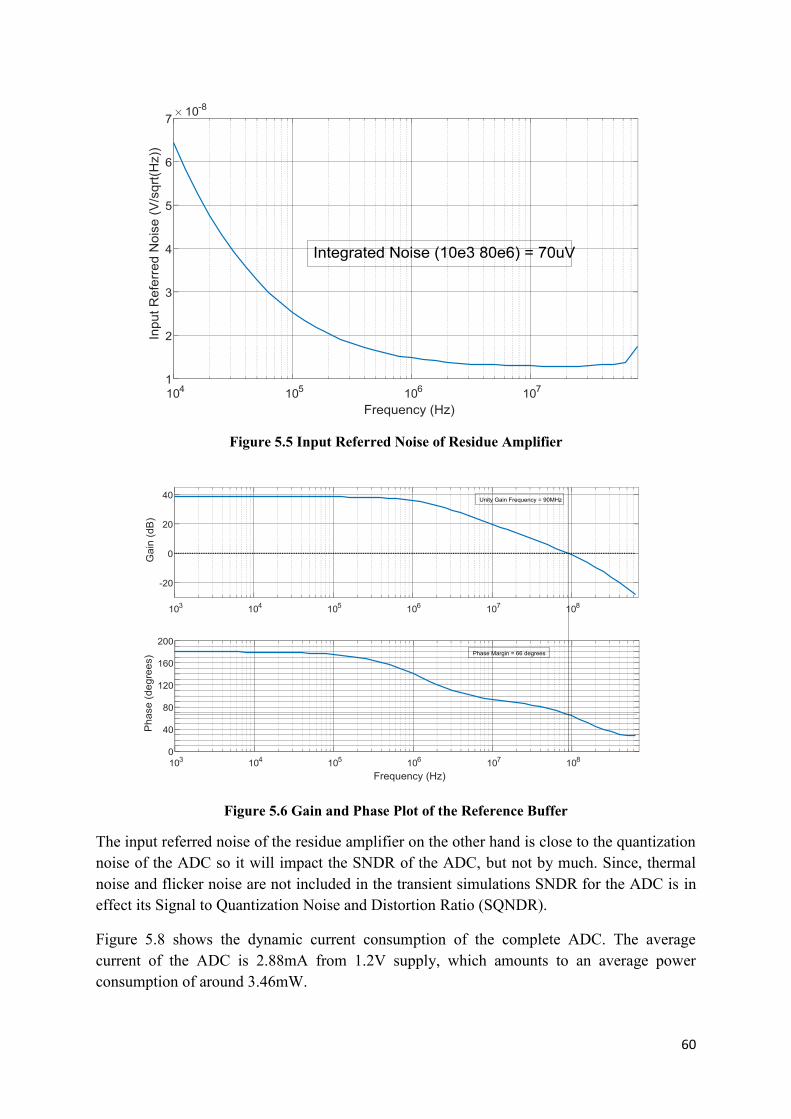
60
Figure 5.5 Input Referred Noise of Residue Amplifier
Figure 5.6 Gain and Phase Plot of the Reference Buffer
The input referred noise of the residue amplifier on the other hand is close to the quantization
noise of the ADC so it will impact the SNDR of the ADC, but not by much. Since, thermal
noise and flicker noise are not included in the transient simulations SNDR for the ADC is in
effect its Signal to Quantization Noise and Distortion Ratio (SQNDR).
Figure 5.8 shows the dynamic current consumption of the complete ADC. The average
current of the ADC is 2.88mA from 1.2V supply, which amounts to an average power
consumption of around 3.46mW.
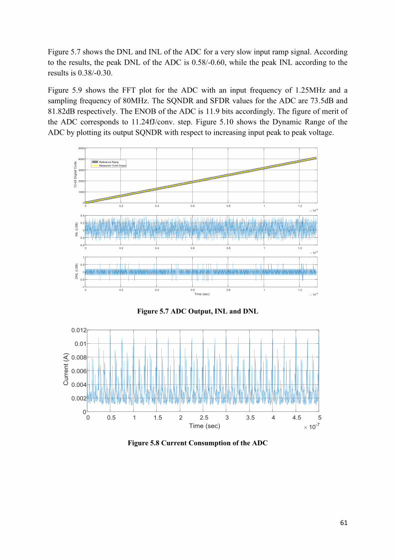
61
Figure 5.7 shows the DNL and INL of the ADC for a very slow input ramp signal. According
to the results, the peak DNL of the ADC is 0.58/-0.60, while the peak INL according to the
results is 0.38/-0.30.
Figure 5.9 shows the FFT plot for the ADC with an input frequency of 1.25MHz and a
sampling frequency of 80MHz. The SQNDR and SFDR values for the ADC are 73.5dB and
81.82dB respectively. The ENOB of the ADC is 11.9 bits accordingly. The figure of merit of
the ADC corresponds to 11.24fJ/conv. step. Figure 5.10 shows the Dynamic Range of the
ADC by plotting its output SQNDR with respect to increasing input peak to peak voltage.
Figure 5.7 ADC Output, INL and DNL
Figure 5.8 Current Consumption of the ADC
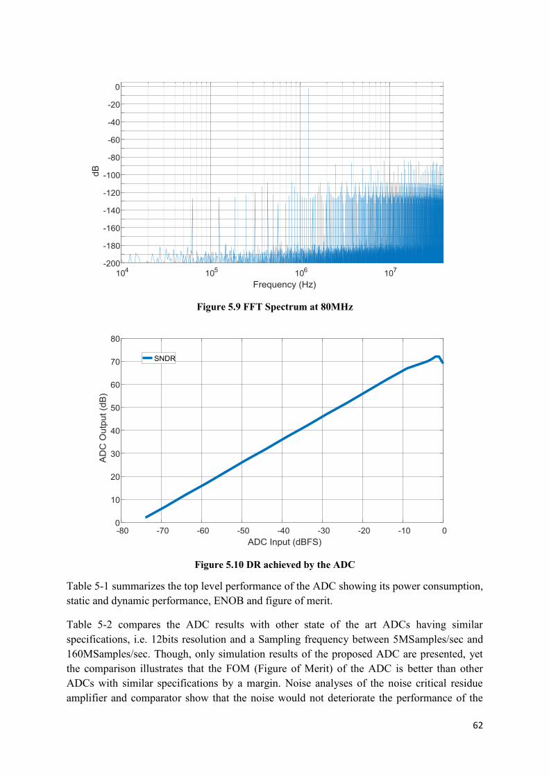
62
Figure 5.9 FFT Spectrum at 80MHz
Figure 5.10 DR achieved by the ADC
Table 5-1 summarizes the top level performance of the ADC showing its power consumption,
static and dynamic performance, ENOB and figure of merit.
Table 5-2 compares the ADC results with other state of the art ADCs having similar
specifications, i.e. 12bits resolution and a Sampling frequency between 5MSamples/sec and
160MSamples/sec. Though, only simulation results of the proposed ADC are presented, yet
the comparison illustrates that the FOM (Figure of Merit) of the ADC is better than other
ADCs with similar specifications by a margin. Noise analyses of the noise critical residue
amplifier and comparator show that the noise would not deteriorate the performance of the

63
ADC. Overall, the results show great promise that post fabrication results of the ADC would
also be comparable with other state of the art ADCs with similar specifications.
Parameter Result Unit
Process Technology 55nm
Resolution 12 Bits
Sampling Frequency 80 MSamples/sec
Supply Voltage 1.2 V
Power Consumption 3.46 mW
SFDR 81.8 dB
DNL 0.58/-0.6 LSB
INL 0.38/-0.3 LSB
SNDR 73.5 dB
ENOB 11.9 Bits
FOM 11.24 fJ/conv. Step
Table 5-1 Performance Results of the ADC
Specification This
Work
[10] [29] [30] [31] [32] [33]
Technology 55nm 40nm 130nm 65nm 180nm 65nm 180nm
Power
Consumption(W)
3.46m 4.96m 4.62m 2.1m 4.5m 5.96m 490uW
Resolution 12 12 12 12 12 12 12
Sampling
Frequency
80MS/S 160MS/s 50MS/s 20MS/s 40MS/s 100MS/s 5MS/s
ENOB 11.9 10.6 10.6 11.27 11.04 11.77 10.76
FOM(fJ/conv.
Step)
11.24 20.7 29.7 36.2 54.9 17 47.8
Table 5-2 Comparison Table

64
6. Conclusions, Discussions and Further
Directions
This work presented a 12 bit 80MS/s low power consumption pipelined SAR ADC. A novel
SAR architecture utilizing a two stage pipelined SAR ADC with sub ranging and an open
loop integrator based residue amplifier allows the ADC to achieve high power efficiency. A
novel calibration method is proposed for gain calibration of the open loop residue amplifier
of the SAR ADC by resolving an additional bit in the first stage SAR ADC and using that bit
to estimate the gain of the amplifier using background calibration. The implemented design
achieves an ENOB of 11.9 bits for an input frequency of 1.25MHz and a sampling frequency
of 80MHz with a power consumption of 3.46mW. The ADC achieves an FOM (Figure of
Merit) of 11.24fJ/conv-step. The DNL of the ADC is 0.58/-0.6 while the INL of the ADC is
0.38/-0.3.
One of the major issues faced during the design of the ADC was the comparator kick back
from both the SAR comparators in stage 1 and stage 2 as well as the flash comparators. In
order to reduce the SAR comparator kickback the switch transistor was moved from the
common source terminal to the drain of the input pair. The dynamic offset of the SAR
comparators because of the use of monotonic switching scheme was also a major issue. The
task of keeping the linearity and noise of the residue amplifier within specifications was also
very difficult.
For future work, new comparator architectures having lower propagation delay along with a
lower power consumption can be investigated to reduce the power consumption of the overall
ADC further. The power consumption of the residue amplifier can also be reduced further by
considering a fully dynamic amplifier. Moreover, the power consumption of the residue
amplifier can be further decreased by decreasing the capacitance of the stage 2 DAC. At the
moment, the stage 2 DAC capacitance is limited by the minimum size of the MOM capacitor
available in the technology. If self designed single metal layer capacitors are used, the
minimum unit capacitance of the 2nd
stage DAC as well as the power consumption of the
residue amplifier can be decreased.

65
References
[1] Wikipedia, “Quantization noise.” http://en.wikipedia.org/wiki/Quantization error.
[2] M.J.M Pelgrom, Analog-to-Digital Conversion. Springer, 2010
[3] Yan Zhu, Chi-Hang et al, “A 10-bit 100-MS/s Reference-Free SAR ADC in 90 nm
CMOS”, IEEE Journal of Solid State Circuits, Vol. 45, No. 6, June 2010.
[4] Guan-Ying Huang, Soon-Jhy Chang et al, “10-bit 30-MS/s SAR ADC using a switchback
Switching Method”, IEEE Transaction on VLSI Systems, Vol. 21, Issue 3, March 2013.
[5] Jeffrey A. Fredenburg et al, “A 90-MS/s 11-MHz Bandwidth 62-dB SNDR Noise
Shaping SAR ADC”, IEEE Journal of Solid State Circuits, Vol. 47, No. 12, December 2012.
[6] Rakesh Kumar Palani and Ramesh Harjani, “A 220 MS/s 9-bit 2X Time-Interleaved SAR
ADC with a 133fF Input Capacitance and a FOM of 37fJ/Conversion step in 65nm CMOS”,
IEEE Transactions on Circuits and Systems II, Volume 62, Issue 11, July 2015.
[7] Lei Sun, Bing Lee et al “A charge recycling SAR ADC with a LSB-down Switching
Scheme”, IEEE Transaction on Circuits and Systems I: Regular Papers, Volume 62, Issue 2,
February 2015.
[8] Michiel van Elzakker, Ed van Tujil et al “A 10-bit Charge redistribution ADC Consuming
1.9µW at 1MS/s”, IEEE Journal of Solid State Circuits, Vol. 45, No. 5, May 2010.
[9] Akira Shikata et al, “A 0.5V 1.1MS/sec 6.3fJ/Conversion-step SAR-ADC with Tri-Level
Comparator in 40nm CMOS”, IEEE Journal of Solid State Circuits, Volume 47, Issue 4,
2012.
[10] Yuan Zhou, Benwei Xu et al “A 12 bit 160 MS/s Two-step SAR ADC with background
bit weight Calibration Using a Time Domain Proximity Detector” IEEE Journal of Solid
State Circuits, Volume 50, Issue 4, April 2015.
[11] Frank van der Goes, Christopher M. Ward et al “A 1.5mW 68dB SNDR 80MS/s 2 x
interleaved Pipelined SAR ADC in 28nm CMOS”, IEEE Journal of Solid State Circuits,
Volume 49, Issue 12, December 2014.
[12] Bob Verbuggen, Masao Iriguchi et al “A 1.7mW 11b 250MS/s 2-Times Interleaved
Fully Dynamic Pipelined SAR ADC in 40nm Digital CMOS”, IEEE Journal of Solid State
Circuits, Volume 47, Issue 12, December 2012.
[13] A. M. Abo, “Design for reliability of low-voltage, switched-capacitor circuits,” Ph.D.
dissertation, California Institute of Technology, Pasadena, CA, USA, 1999.
[14] A. M. Abo and P. R. Gray, “A 1.5-V, 10-bit, 14.3-MS/s CMOS pipeline analog-to-
digital converter”, IEEE Journal of Solid State Circuits, Volume 34, Issue 5, May 1999
66
[15] E. Suarez, P. R. Gray et al “All-MOS Charge Redistribution analog-to-digital conversion
techniques – Part I”, IEEE Journal of Solid State Circuits, vol–SC-10, no. 6, pp. 371-379,
December 1975.
[16] R. J. Baker, CMOS Circuit Design, Layout and Simulation, 2nd
Edition, New York,
Wiley 2004.
[17] Mehdi Saberi, Reza Lotfi et al “Analysis of Power Consumption and Linearity in
Capacitive Digital-to-Analog Converters Used in Successive Approximation ADCs”, IEEE
Transactions on Circuits and Systems – I; Regular Papers, Vol. 58, No. 8, August 2011.
[18] Chun Ceng Liu, Sun Jyh Chang et al, “A 10-bit 50-MS/s SAR ADC With a Monotonic
Capacitor Switching Procedure”, IEEE Journal of Solid State Circuit, vol. 45, No. 4, April
2010
[19] Jieh-Tsorng Wu and Wooley B. A, “A 100-MHz pipeline CMOS comparator,” IEEE
Journal of Solid-State Circuits, vol. 23, no. 6, pp. 1371–1385, 1988.
[20] James Montanaro Richard T. Witek et al, “160-MHz, 32-b, 0.5-W CMOS RISC
microprocessor,” IEEE Journal of Solid-State Circuits, vol. 31, no. 11, pp. 1703–1714, 1996.
[21] M. van Elzakker et al, “1.9 W 4.4 fJ/conversion-step 10b 1 MS/s charge-redistribution
ADC”, ISSCC Dig. Tech. Papers, pp. 244–245, Feb 2008.
[22] Tomohiko Ogawa et al “SAR ADC algorithm with Redundancy and Digital Error
Correction”, IEICE Trans. Fundamentals, Volume E93-A, No. 2, February 2010
[23] Albert Hsu Ting Chang “Low Power High-Performance SAR ADC with Redundancy
and Digital Background Calibration”, partial fulfilment of the requirements for the degree of
Doctor of Philosophy, MIT, June 2013.
[24] J.J. Wikner M. Gustavsson and N.N. Tan. CMOS Data converters for communications.
Kluwer Academic Publishers, 2000.
[25] Ying Zu Lin, Chun Cheng Liu et al, “A 9-bit 150MS/s Subrange ADC Based on SAR
Architecture in 90nm-CMOS”, IEEE Transactions on Circuits and Systems – I: Regular
Papers, Vol. 60, No. 3, March 2013.
[26] J. Steensgaard, “Bootstrapped Low Voltage Analog Switches”, IEEE International
Symposium on Circuits and Systems, 1999.
[27] C. C. Liu, S. J. Chang et al, “A 0.92mW10-bit 50-MS/s SAR ADC in 0.13 um CMOS
process”, IEEE Symposium VLSI Circuits Dig., Jun. 2009, pp. 236–237.
[28] B. Widrow, “A study of rough amplitude quantization by means of Nyquist sampling
theory,” IRE Trans. Circuit Theory, vol. CT-3, pp. 266-76, 1956

67
[29] In-Seok Jung and Yong-Bin Kim, “A novel self-calibration scheme for 12-bit 50MS/s
SAR ADC”, IEEE 57th International Midwest Symposium on Circuits and Systems, August
2014.
[30] Xuan Li et al, “A 12-bit 20-MS/s SAR ADC with improved internal clock generator and
SAR controller”, IEEE 58th
International Midwest Symposium on Circuits and System,
August 2015
[31] Vahid Khojasteh Lazarjan and Khosrow Hajsadeghi, “12 bits, 40MS/s, low power
pipelined SAR ADC”, IEEE 57th
International Midwest Symposium on Circuits and Systems,
August 2014.
[32] Qing Wang et al, “A 12-bit 100MS/s low power Successive Approximation Register
ADC in 65nm CMOS”, IEEE Conference on Electron Devices and Solid-State Circuits, June
2014
[33] Jiu Yu Wen et al “Chip design of a 12-bit 5MS/s fully differential SAR ADC with
resistor-capacitor array DAC technique for wireless application”, IEEE International
Conference on Signal Processing, Communications and Computing, Sept 2015
Related Documents