DATA SHEET Product specification Supersedes data of 2003 May 15 2003 Oct 30 INTEGRATED CIRCUITS 74HCT9046A PLL with band gap controlled VCO

Welcome message from author
This document is posted to help you gain knowledge. Please leave a comment to let me know what you think about it! Share it to your friends and learn new things together.
Transcript

DATA SHEET
Product specificationSupersedes data of 2003 May 15
2003 Oct 30
INTEGRATED CIRCUITS
74HCT9046APLL with band gap controlled VCO

2003 Oct 30 2
Philips Semiconductors Product specification
PLL with band gap controlled VCO 74HCT9046A
FEATURES
• Operation power supply voltage range from 4.5 to 5.5 V
• Low power consumption
• Inhibit control for ON/OFF keying and for low standbypower consumption
• Centre frequency up to 17 MHz (typical) at VCC = 5.5 V
• Choice of two phase comparators:
– PC1: EXCLUSIVE-OR
– PC2: Edge-triggered JK flip-flop.
• No dead zone of PC2
• Charge pump output on PC2, whose current is set by anexternal resistor Rb
• Centre frequency tolerance ±10%
• Excellent Voltage Controlled Oscillator (VCO) linearity
• Low frequency drift with supply voltage and temperaturevariations
• On-chip band gap reference
• Glitch free operation of VCO, even at very lowfrequencies
• Zero voltage offset due to op-amp buffering
• ESD protection:
– HBM EIA/JESD22-A114-A exceeds 2000 V
– MM EIA/JESD22-A115-A exceeds 200 V.
APPLICATIONS
• FM modulation and demodulation where a small centrefrequency tolerance is essential
• Frequency synthesis and multiplication where a low jitteris required (e.g. video picture-in-picture)
• Frequency discrimination
• Tone decoding
• Data synchronization and conditioning
• Voltage-to-frequency conversion
• Motor-speed control.
GENERAL DESCRIPTION
The 74HCT9046A is a high-speed Si-gate CMOS device.It is specified in compliance with JEDEC standard no 7A.
QUICK REFERENCE DATAGND = 0 V; Tamb = 25 °C; tr = tf ≤ 6 ns.
Notes
1. CPD is used to determine the dynamic power dissipation (PD in µW).
PD = CPD × VCC2 × fi × N + Σ(CL × VCC
2 × fo) where:
fi = input frequency in MHz;
fo = output frequency in MHz;
CL = output load capacitance in pF;
VCC = supply voltage in Volts;
N = total load switching outputs;
Σ(CL × VCC2 × fo) = sum of the outputs.
2. Applies to the phase comparator section only (pin INH = HIGH). For power dissipation of the VCO and demodulatorsections, see Figs 26 to 28.
SYMBOL PARAMETER CONDITIONS TYPICAL UNIT
fc VCO centre frequency C1 = 40 pF; R1 = 3 kΩ; VCC = 5 V 16 MHz
CI input capacitance 3.5 pF
CPD power dissipation capacitance per package notes 1 and 2 20 pF
2003 Oct 30 3
Philips Semiconductors Product specification
PLL with band gap controlled VCO 74HCT9046A
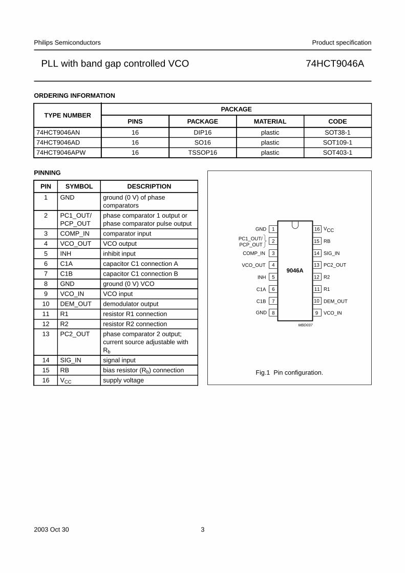
ORDERING INFORMATION
TYPE NUMBERPACKAGE
PINS PACKAGE MATERIAL CODE
74HCT9046AN 16 DIP16 plastic SOT38-1
74HCT9046AD 16 SO16 plastic SOT109-1
74HCT9046APW 16 TSSOP16 plastic SOT403-1
PINNING
PIN SYMBOL DESCRIPTION
1 GND ground (0 V) of phasecomparators
2 PC1_OUT/PCP_OUT
phase comparator 1 output orphase comparator pulse output
3 COMP_IN comparator input
4 VCO_OUT VCO output
5 INH inhibit input
6 C1A capacitor C1 connection A
7 C1B capacitor C1 connection B
8 GND ground (0 V) VCO
9 VCO_IN VCO input
10 DEM_OUT demodulator output
11 R1 resistor R1 connection
12 R2 resistor R2 connection
13 PC2_OUT phase comparator 2 output;current source adjustable withRb
14 SIG_IN signal input
15 RB bias resistor (Rb) connection
16 VCC supply voltageFig.1 Pin configuration.
1
2
3
4
5
6
7
8
16
15
14
13
12
11
10
9
GND
PC1_OUT/PCP_OUT
COMP_IN
VCO_OUT
C1B
C1A
GND VCO_IN
DEM_OUT
R2
R1
PC2_OUT
SIG_IN
VCC
RB
9046A
MBD037
INH

2003 Oct 30 4
Philips Semiconductors Product specification
PLL with band gap controlled VCO 74HCT9046A
LOGIC AND FUNCTIONAL SYMBOLS ANDDIAGRAMS
Fig.2 Logic symbol.
MBD038
PC1_OUT/PCP_OUT
VCO_OUT
C1A
C1B
VCO_IN DEM_OUT
R2
R1
SIG_IN
INH
VCO
67
1112
95
4
10
2
13
31415
PC2_OUT
ΦCOMP_IN
RB
Fig.3 IEC logic symbol.
MBD039
SIG_IN
INH
67
1112
95
4
10
2
13
314
15
Φ
COMP_IN
PLL9046A
PC1_OUT/PCP_OUT
VCO_OUT
C1A
C1B
VCO_IN
DEM_OUTR2
R1
PC2_OUT
RB
Fig.4 Block diagram.
PHASECOMPARATOR
2
13
PHASECOMPARATOR
1
2
15
SIG_INCOMP_INC1A C1B
fout
fin VCC
DEM_OUTINH VCO_IN
R2
12
11
3 14 16476
5 10 9
GND
8
GND
1
C1
9046A
VCO
Rs
R1 R4
R3
C2
PC2_OUT
MBD040
PC1_OUT/PCP_OUT
VCO_OUT
R2
R1
RB
Rb
2003O
ct305
Philips S
emiconductors
Product specification
PLL w
ith band gap controlled VC
O74H
CT
9046A
This text is here in white to force landscape pages to be rotated correctly when browsing through the pdf in the Acrobat reader.This text is here in_white to force landscape pages to be rotated correctly when browsing through the pdf in the Acrobat reader.This text is here inThis text is here inwhite to force landscape pages to be rotated correctly when browsing through the pdf in the Acrobat reader. white to force landscape pages to be ...
hand
book
, ful
l pag
ewid
th
MBD102
PCPD Q
CP
QRD
logic1
D Q
CP
QRD
logic1
down
up
CHARGEPUMP
Vref2
Vref2
Vref2
Vref1
Vref1
PC1_OUT/PCP_OUT
PC2_OUT
b
Rb
RB
C2
R4
2
13
R3
15
COMP_IN SIG_IN
3 14
PC1
BANDGAP
5
INH
9
VCO
DEM_OUT
VCO_OUTC1BC1A
76 4
C1
12
R2
11
R1
10
R
fout fin
R2
R1
s
VCO_IN
R3' = R /17
R3'(1)
(1)
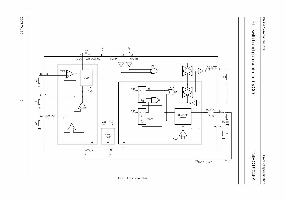
Fig.5 Logic diagram.

2003 Oct 30 6
Philips Semiconductors Product specification
PLL with band gap controlled VCO 74HCT9046A
FUNCTIONAL DESCRIPTION
The 74HCT9046A is a phase-locked-loop circuit thatcomprises a linear VCO and two different phasecomparators (PC1 and PC2) with a common signal inputamplifier and a common comparator input (see Fig.4).The signal input can be directly coupled to large voltagesignals (CMOS level), or indirectly coupled (with a seriescapacitor) to small voltage signals. A self-bias input circuitkeeps small voltage signals within the linear region of theinput amplifiers. With a passive low-pass filter, the74HCT9046A forms a second-order loop PLL.
The principle of this phase-locked-loop is based on thefamiliar 74HCT4046A. However extra features are built-in,allowing very high-performance phase-locked-loopapplications. This is done, at the expense of PC3, which isskipped in this 74HCT9046A. The PC2 is equipped with acurrent source output stage here. Further a band gap isapplied for all internal references, allowing a small centrefrequency tolerance. The details are summed up in thenext section: “Differences with respect to the familiar74HCT4046A”. If one is familiar with the 74HCT4046Aalready, it will do to read this section only.
Differences with respect to the familiar 74HCT4046A
• A centre frequency tolerance of maximum ±10%.
• The on board band gap sets the internal referencesresulting in a minimal frequency shift at supply voltagevariations and temperature variations.
• The value of the frequency offset is determined by aninternal reference voltage of 2.5 V instead ofVCC − 0.7 V. In this way the offset frequency will not shiftover the supply voltage range.
• A current switch charge pump output on pin PC2_OUTallows a virtually ideal performance of PC2. The gain ofPC2 is independent of the voltage across the low-passfilter. Further a passive low-pass filter in the loopachieves an active performance. The influence of theparasitic capacitance of the PC2 output plays no rolehere, resulting in a true correspondence of the outputcorrection pulse and the phase difference even up tophase differences as small as a few nanoseconds.
• Because of its linear performance without dead zone,higher impedance values for the filter, hence lowerC-values, can now be chosen. Correct operation will notbe influenced by parasitic capacitances as in theinstance with voltage source output of the 4046A.
• No PC3 on pin RB but instead a resistor connected toGND, which sets the load/unload currents of the chargepump (PC2).
• Extra GND pin 1 to allow an excellent FM demodulatorperformance even at 10 MHz and higher.
• Combined function of pin PC1_OUT/PCP_OUT.If pin RB is connected to VCC (no bias resistor Rb)pin PC1_OUT/PCP_OUT has its familiar function viz.output of PC1. If at pin RB a resistor (Rb) is connectedto GND it is assumed that PC2 has been chosen asphase comparator. Connection of Rb is sensed byinternal circuitry and this changes the function ofpin PC1_OUT/PCP_OUT into a lock detect output(PCP_OUT) with the same characteristics as PCP_OUTof pin 1 of the 74HCT4046A.
• The inhibit function differs. For the HCT4046A a HIGHlevel at the inhibit input (pin INH) disables the VCO anddemodulator, while a LOW level turns both on. For the74HCT9046A a HIGH level on the inhibit input disablesthe whole circuit to minimize standby powerconsumption.
VCO
The VCO requires one external capacitor C1 (betweenpins C1A and C1B) and one external resistor R1 (betweenpins R1 and GND) or two external resistors R1 and R2(between pins R1 and GND, and R2 and GND).Resistor R1 and capacitor C1 determine the frequencyrange of the VCO. Resistor R2 enables the VCO to have afrequency offset if required (see Fig.5).
The high input impedance of the VCO simplifies the designof the low-pass filters by giving the designer a wide choiceof resistor/capacitor ranges. In order not to load thelow-pass filter, a demodulator output of the VCO inputvoltage is provided at pin DEM_OUT. The DEM_OUTvoltage equals that of the VCO input. If DEM_OUT is used,a load resistor (Rs) should be connected frompin DEM_OUT to GND; if unused, DEM_OUT should beleft open. The VCO output (pin VCO_OUT) can beconnected directly to the comparator input(pin COMP_IN), or connected via a frequency divider.The output signal has a duty factor of 50% (maximumexpected deviation 1%), if the VCO input is held at aconstant DC level. A LOW level at the inhibit input(pin INH) enables the VCO and demodulator, while aHIGH level turns both off to minimize standby powerconsumption.
2003 Oct 30 7
Philips Semiconductors Product specification
PLL with band gap controlled VCO 74HCT9046A
Phase comparators
The signal input (pin SIG_IN) can be directly coupled tothe self-biasing amplifier at pin SIG_IN, provided that thesignal swing is between the standard HC family input logiclevels. Capacitive coupling is required for signals withsmaller swings.
PHASE COMPARATOR 1 (PC1)
This circuit is an EXCLUSIVE-OR network. The signal andcomparator input frequencies (fi) must have a 50% dutyfactor to obtain the maximum locking range. The transfercharacteristic of PC1, assuming ripple (fr = 2fi)
is suppressed, is:
where:
VDEM_OUT is the demodulator output at pin DEM_OUT.
VDEM_OUT = VPC1_OUT (via low-pass).
The phase comparator gain is:
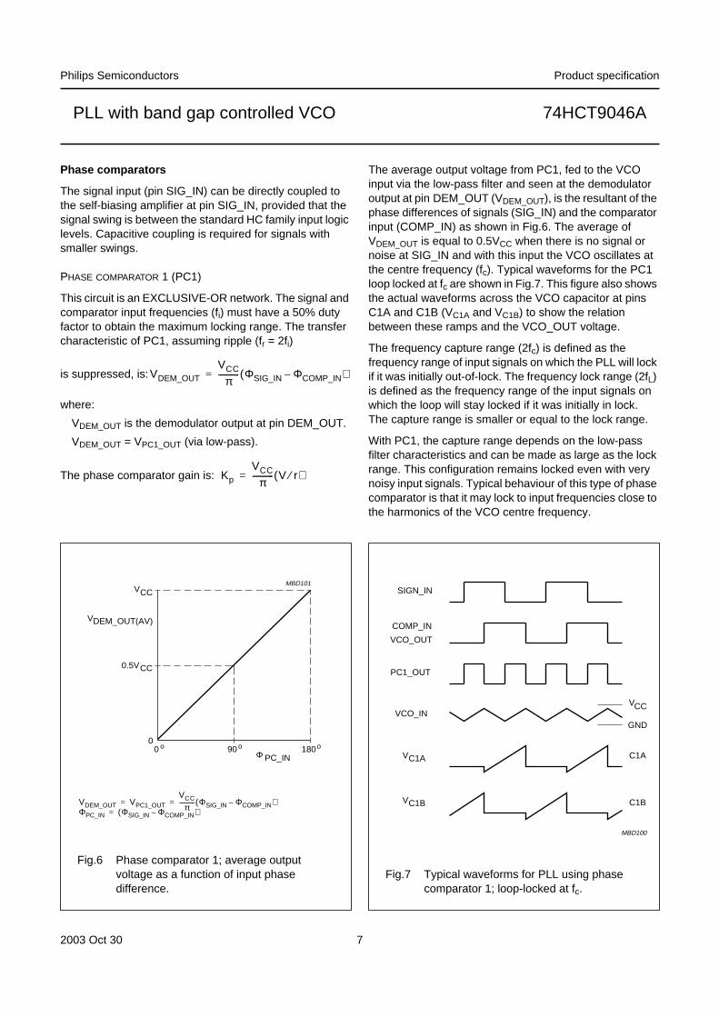
The average output voltage from PC1, fed to the VCOinput via the low-pass filter and seen at the demodulatoroutput at pin DEM_OUT (VDEM_OUT), is the resultant of thephase differences of signals (SIG_IN) and the comparatorinput (COMP_IN) as shown in Fig.6. The average ofVDEM_OUT is equal to 0.5VCC when there is no signal ornoise at SIG_IN and with this input the VCO oscillates atthe centre frequency (fc). Typical waveforms for the PC1loop locked at fc are shown in Fig.7. This figure also showsthe actual waveforms across the VCO capacitor at pinsC1A and C1B (VC1A and VC1B) to show the relationbetween these ramps and the VCO_OUT voltage.
The frequency capture range (2fc) is defined as thefrequency range of input signals on which the PLL will lockif it was initially out-of-lock. The frequency lock range (2fL)is defined as the frequency range of the input signals onwhich the loop will stay locked if it was initially in lock.The capture range is smaller or equal to the lock range.
With PC1, the capture range depends on the low-passfilter characteristics and can be made as large as the lockrange. This configuration remains locked even with verynoisy input signals. Typical behaviour of this type of phasecomparator is that it may lock to input frequencies close tothe harmonics of the VCO centre frequency.
VDEM_OUT
VCC
π----------- ΦSIG_IN ΦCOMP_IN–( )=
Kp
VCC
π----------- V r⁄( )=
Fig.6 Phase comparator 1; average outputvoltage as a function of input phasedifference.
MBD101
180o
PC_IN 0 o 90 o
0.5V
0
V
VDEM_OUT(AV)
CC
CC
Φ
VDEM_OUT VPC1_OUT
VCC
π----------- ΦSIG_IN ΦCOMP_IN–( )= =ΦPC_IN ΦSIG_IN ΦCOMP_IN–( )=
Fig.7 Typical waveforms for PLL using phasecomparator 1; loop-locked at fc.
MBD100
PC1_OUT
VCO_INVCC
GND
VCO_OUT
COMP_IN
SIGN_IN
C1A
C1B
VC1A
VC1B
2003 Oct 30 8
Philips Semiconductors Product specification
PLL with band gap controlled VCO 74HCT9046A
PHASE COMPARATOR 2 (PC2)
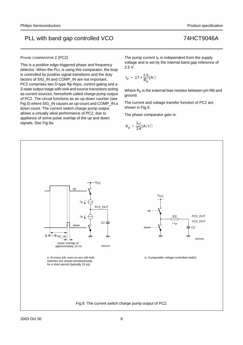
This is a positive edge-triggered phase and frequencydetector. When the PLL is using this comparator, the loopis controlled by positive signal transitions and the dutyfactors of SIG_IN and COMP_IN are not important.PC2 comprises two D-type flip-flops, control gating and a3-state output stage with sink and source transistors actingas current sources, henceforth called charge pump outputof PC2. The circuit functions as an up-down counter (seeFig.5) where SIG_IN causes an up-count and COMP_IN adown count. The current switch charge pump outputallows a virtually ideal performance of PC2, due toappliance of some pulse overlap of the up and downsignals. See Fig.8a.
The pump current IP is independent from the supplyvoltage and is set by the internal band gap reference of2.5 V.
Where Rb is the external bias resistor between pin RB andground.
The current and voltage transfer function of PC2 areshown in Fig.9.
The phase comparator gain is:
IP 172.5Rb-------- A( )×=
Kp
IP2π------- A r⁄( )=
MBD099
R3'
IP
up
down C2
VCC
PC2_OUT
VC2_OUT
Fig.8 The current switch charge pump output of PC2.
a. At every ∆Φ, even at zero ∆Φ bothswitches are closed simultaneouslyfor a short period (typically 15 ns).
MBD046
PC2_OUT
C2
VCC
IP
IP
down
up
∆ Φ = Φ
pulse overlap of approximately 15 ns
PC_IN
b. Comparable voltage-controlled switch.
2003 Oct 30 9
Philips Semiconductors Product specification
PLL with band gap controlled VCO 74HCT9046A
handbook, full pagewidth
0
MSB306
0
0.5VCC
0
VCC
VDEM_OUT(AV)IP × R
0ΦPC_IN ΦPC_IN
ΦPC_IN = ΦSIG_IN − ΦCOMP_IN
+IP
−IP
−2π +2π −2π +2π
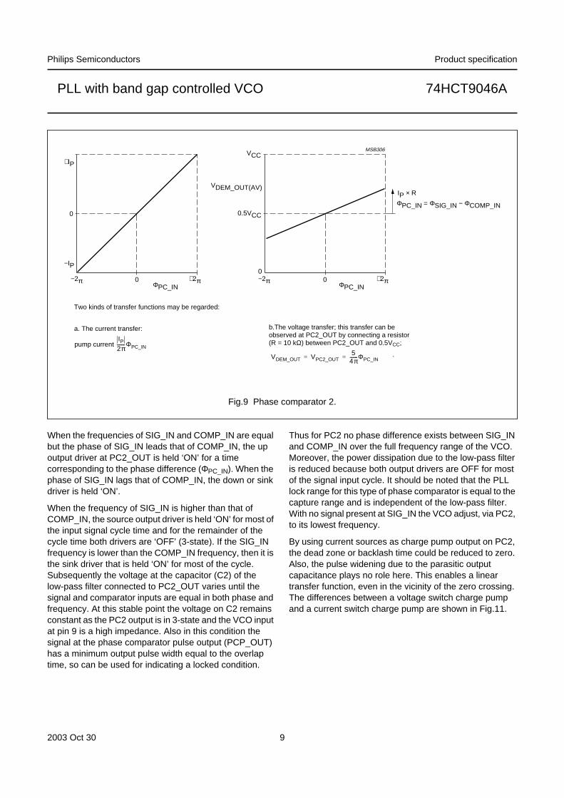
Fig.9 Phase comparator 2.
Two kinds of transfer functions may be regarded:
b.The voltage transfer; this transfer can beobserved at PC2_OUT by connecting a resistor(R = 10 kΩ) between PC2_OUT and 0.5VCC;
.VDEM_OUT VPC2_OUT5
4π-------ΦPC_IN= =
a. The current transfer:
pump currentIP2π-------ΦPC_IN
When the frequencies of SIG_IN and COMP_IN are equalbut the phase of SIG_IN leads that of COMP_IN, the upoutput driver at PC2_OUT is held ‘ON’ for a timecorresponding to the phase difference (ΦPC_IN). When thephase of SIG_IN lags that of COMP_IN, the down or sinkdriver is held ‘ON’.
When the frequency of SIG_IN is higher than that ofCOMP_IN, the source output driver is held ‘ON’ for most ofthe input signal cycle time and for the remainder of thecycle time both drivers are ‘OFF’ (3-state). If the SIG_INfrequency is lower than the COMP_IN frequency, then it isthe sink driver that is held ‘ON’ for most of the cycle.Subsequently the voltage at the capacitor (C2) of thelow-pass filter connected to PC2_OUT varies until thesignal and comparator inputs are equal in both phase andfrequency. At this stable point the voltage on C2 remainsconstant as the PC2 output is in 3-state and the VCO inputat pin 9 is a high impedance. Also in this condition thesignal at the phase comparator pulse output (PCP_OUT)has a minimum output pulse width equal to the overlaptime, so can be used for indicating a locked condition.
Thus for PC2 no phase difference exists between SIG_INand COMP_IN over the full frequency range of the VCO.Moreover, the power dissipation due to the low-pass filteris reduced because both output drivers are OFF for mostof the signal input cycle. It should be noted that the PLLlock range for this type of phase comparator is equal to thecapture range and is independent of the low-pass filter.With no signal present at SIG_IN the VCO adjust, via PC2,to its lowest frequency.
By using current sources as charge pump output on PC2,the dead zone or backlash time could be reduced to zero.Also, the pulse widening due to the parasitic outputcapacitance plays no role here. This enables a lineartransfer function, even in the vicinity of the zero crossing.The differences between a voltage switch charge pumpand a current switch charge pump are shown in Fig.11.

2003 Oct 30 10
Philips Semiconductors Product specification
PLL with band gap controlled VCO 74HCT9046A
MBD047
SIG_IN
COMP_IN
VCO_OUT
high-impedance OFF-state,(zero current)
15 ns typicalUP
DOWN
CURRENT ATPC2_OUT
PC2_OUT/VCO_IN
PCP_OUT
PC_IN
Fig.10 Timing diagram for PC2.
The pulse overlap of the up and down signals (typically 15 ns).
Fig.11 The response of a locked-loop in the vicinity of the zero crossing of the phase error.
handbook, full pagewidth
MBD043
25
2.50
2.75
2.25
VCO_IN VCO_IN
0 25phase error (ns)
(1)
(1)
(2)
25
2.50
2.75
2.250 25
phase error (ns)
a. Response with traditional voltage-switch charge-pumpPC2_OUT (74HCT4046A).
(1) Due to parasitic capacitance on PC2_OUT.
(2) Backlash time (dead zone).
b. Response with current switch charge-pumpPC2_OUT as applied in the 74HCT9046A.

2003 Oct 30 11
Philips Semiconductors Product specification
PLL with band gap controlled VCO 74HCT9046A
The design of the low-pass filter is somewhat differentwhen using current sources. The external resistor R3 is nolonger present when using PC2 as phase comparator.The current source is set by Rb. A simple capacitorbehaves as an ideal integrator now, because the capacitoris charged by a constant current. The transfer function ofthe voltage switch charge pump may be used. In fact it iseven more valid, because the transfer function is no longerrestricted for small changes only. Further the current isindependent from both the supply voltage and the voltageacross the filter. For one that is familiar with the low-passfilter design of the 74HCT4046A a relation may show howRb relates with a fictive series resistance, called R3'.
This relation can be derived by assuming first that avoltage controlled switch PC2 of the 74HCT4046A isconnected to the filter capacitance C2 via this fictive R3'(see Fig.8b). Then during the PC2 output pulse the chargecurrent equals:
With the initial voltage VC2(0) at:
0.5VCC = 2.5 V,
As shown before the charge current of the current switchof the 74HCT9046A is:
Hence:
Using this equivalent resistance R3' for the filter design thevoltage can now be expressed as a transfer function ofPC2; assuming ripple (fr = fi) is suppressed, as:
Again this illustrates the supply voltage independentbehaviour of PC2.
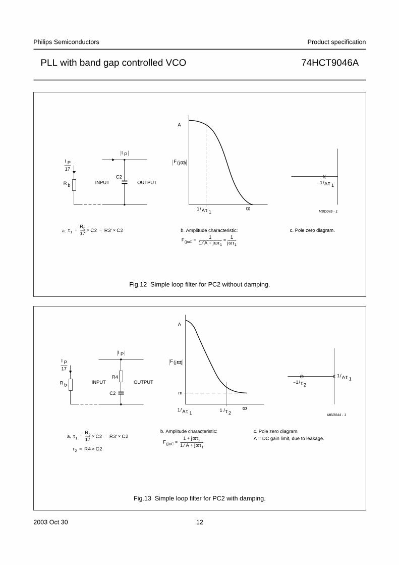
LOOP FILTER COMPONENT SELECTION
Examples of PC2 combined with a passive filter are shownin Figs 12 and 13. Figure 12 shows that PC2 with only aC2 filter behaves as a high-gain filter. For stability thedamped version of Fig.13 with series resistance R4 ispreferred.
Practical design values for Rb are between 25 and 250 kΩwith R3' = 1.5 to 15 kΩ for the filter design. Higher valuesfor R3' require lower values for the filter capacitance whichis very advantageous at low values the loop naturalfrequency ωn.
IPVCC VC2 0( )–
R3'---------------------------------=
IP2.5R3'---------=
IP 17 2.5Rb--------×=
R3'Rb
17------- Ω( )=
KPC25
4π------- V r⁄( )=
2003 Oct 30 12
Philips Semiconductors Product specification
PLL with band gap controlled VCO 74HCT9046A
MBD045 - 1
ωj( )F
ω
1/OUTPUTINPUTC2
I PI P17
R b
1/ τ 1A
A
τ 1A
Fig.12 Simple loop filter for PC2 without damping.
a. τ1
Rb
17------- C2× R3' C2×= = b. Amplitude characteristic:
F jω( )1
1 A⁄ jωτ1+-----------------------------
1jωτ1-----------≈=
c. Pole zero diagram.
MBD044 - 1
ωj( )F
m
1 /τ2ω
O1/τ2
1/ τ 1OUTPUTINPUT
R4
C2
I PI P17
R b
A
1/ τ 1A
A
Fig.13 Simple loop filter for PC2 with damping.
a.b. Amplitude characteristic: c. Pole zero diagram.
A = DC gain limit, due to leakage.τ1
Rb
17------- C2× R3' C2×= =
τ2 R4 C2×=
F jω( )1 jωτ2+
1 A⁄ jωτ1+-----------------------------=
2003 Oct 30 13
Philips Semiconductors Product specification
PLL with band gap controlled VCO 74HCT9046A
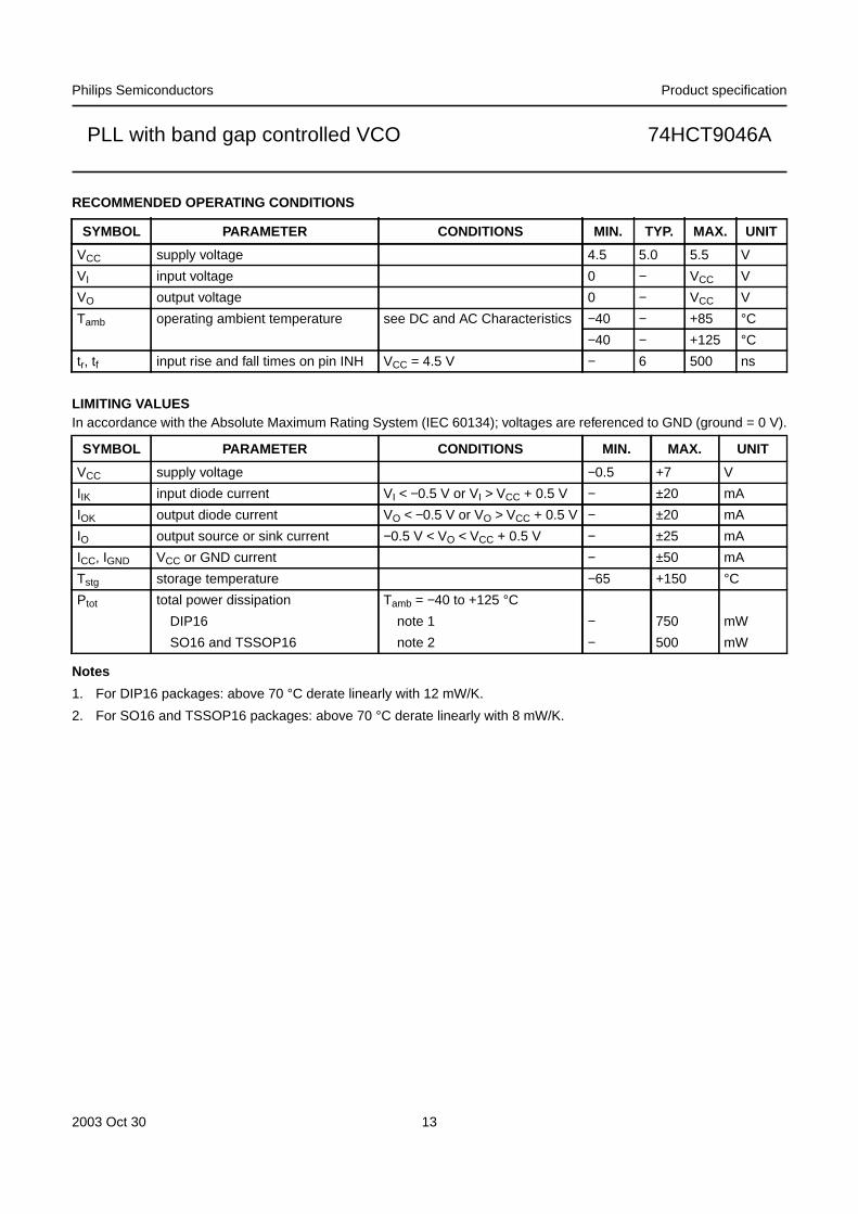
RECOMMENDED OPERATING CONDITIONS
LIMITING VALUESIn accordance with the Absolute Maximum Rating System (IEC 60134); voltages are referenced to GND (ground = 0 V).
Notes
1. For DIP16 packages: above 70 °C derate linearly with 12 mW/K.
2. For SO16 and TSSOP16 packages: above 70 °C derate linearly with 8 mW/K.
SYMBOL PARAMETER CONDITIONS MIN. TYP. MAX. UNIT
VCC supply voltage 4.5 5.0 5.5 V
VI input voltage 0 − VCC V
VO output voltage 0 − VCC V
Tamb operating ambient temperature see DC and AC Characteristics −40 − +85 °C−40 − +125 °C
tr, tf input rise and fall times on pin INH VCC = 4.5 V − 6 500 ns
SYMBOL PARAMETER CONDITIONS MIN. MAX. UNIT
VCC supply voltage −0.5 +7 V
IIK input diode current VI < −0.5 V or VI > VCC + 0.5 V − ±20 mA
IOK output diode current VO < −0.5 V or VO > VCC + 0.5 V − ±20 mA
IO output source or sink current −0.5 V < VO < VCC + 0.5 V − ±25 mA
ICC, IGND VCC or GND current − ±50 mA
Tstg storage temperature −65 +150 °CPtot total power dissipation Tamb = −40 to +125 °C
DIP16 note 1 − 750 mW
SO16 and TSSOP16 note 2 − 500 mW

2003 Oct 30 14
Philips Semiconductors Product specification
PLL with band gap controlled VCO 74HCT9046A
DC CHARACTERISTICSAt recommended operating conditions; voltages are referenced to GND (ground = 0 V).
SYMBOL PARAMETERTEST CONDITIONS
MIN. TYP. MAX. UNITOTHER VCC (V)
Tamb = 25 °C
PHASE COMPARATOR SECTION
VIH HIGH-level input voltageon pins SIG_IN andCOMP_IN
DC coupled 4.5 3.15 2.4 − V
VIL LOW-level input voltage onpins SIG_IN andCOMP_IN
DC coupled 4.5 − 2.1 1.35 V
VOH HIGH-level output voltageon pins PCP_OUT andPCn_OUT
VI = VIH or VIL
IO = −20 µA 4.5 4.4 4.5 − V
IO = −4.0 mA 4.5 3.98 4.32 − V
VOL LOW-level output voltageon pins PCP_OUT andPCn_OUT
VI = VIH or VIL
IO = 20 µA 4.5 − 0 0.1 V
IO = 4.0 mA 4.5 − 0.15 0.26 V
ILI input leakage current inpins SIG_IN andCOMP_IN
VCC or GND 5.5 − − ±30 µA
IOZ 3-state OFF-state currentin pin PC2_OUT
VI = VIH or VIL;VO = VCC or GND
5.5 − − ±0.5 µA
RI input resistance SIG_IN,COMP_IN
VI at self-bias operatingpoint; ∆VI = 0.5 V;see Figs 14 to 16
4.5 − 250 − kΩ
Rb bias resistance 4.5 25 − 250 kΩIP charge pump current Rb = 40 kΩ 4.5 ±0.53 ±1.06 ±2.12 mA
VCO SECTION
VIH HIGH-level input voltageon pin INH
DC coupled 4.5 to 5.5 2.0 1.6 − V
VIL LOW-level input voltage onpin INH
DC coupled 4.5 to 5.5 − 1.2 0.8 V
VOH HIGH-level output voltageon pin VCO_OUT
VI = VIH or VIL
IO = −20 µA 4.5 4.4 4.5 − V
IO = −4.0 mA 4.5 3.98 4.32 − V
VOL LOW-level output voltageon pin VCO_OUT
VI = VIH or VIL
IO = 20 µA 4.5 − 0 0.1 V
IO = 4.0 mA 4.5 − 0.15 0.26 V
VOL LOW-level output voltageon pins C1A and C1B
VI = VIH or VIL;IO = 4.0 mA
4.5 − − 0.40 V
ILI input leakage current inpins INH and VCO_IN
VCC or GND 5.5 − − ±0.1 µA

2003 Oct 30 15
Philips Semiconductors Product specification
PLL with band gap controlled VCO 74HCT9046A
R1 resistor value 4.5 3 − 300 kΩR2 resistor value 4.5 3 − 300 kΩC1 capacitance 4.5 40 − no limit pF
VVCO_IN operating voltage on pinVCO_IN
over the range specifiedfor R1
4.5 1.1 − 3.4 V
5.0 1.1 − 3.9 V
5.5 1.1 − 4.4 V
DEMODULATOR SECTION
Rs resistor value at Rs > 300 kΩ theleakage current caninfluence VDEM_OUT
4.5 50 − 300 kΩ
VOFF offset voltage VCO_IN toVDEM_OUT
VI = VVCO_IN = 0.5VCC;values taken over Rsrange, see Fig.17
4.5 − ±20 − mV
Rdyn dynamic output resistanceat DEM_OUT
VDEM_OUT = 0.5VCC 4.5 − 25 − Ω
GENERAL
ICC quiescent supply current(disabled)
pin INH at VCC 5.5 − − 8.0 µA
∆ICC additional quiescent supplycurrent per input pin
other inputs at VCC orGND; VI = VCC − 2.1 V
4.5 − 100 360 µA
Tamb = −40 to +85 °C
PHASE COMPARATOR SECTION
VIH HIGH-level input voltageon pins SIG_IN andCOMP_IN
DC coupled 4.5 3.15 − − V
VIL LOW-level input voltage onpins SIG_IN andCOMP_IN
DC coupled 4.5 − − 1.35 V
VOH HIGH-level output voltageon pins PCP_OUT andPCn_OUT
VI = VIH or VIL
IO = −20 µA 4.5 4.4 − − V
IO = −4.0 mA 4.5 3.84 − − V
VOL LOW-level output voltageon pins PCP_OUT andPCn_OUT
VI = VIH or VIL
IO = 20 µA 4.5 − − 0.1 V
IO = 4.0 mA 4.5 − − 0.33 V
ILI input leakage current inpins SIG_IN andCOMP_IN
VCC or GND 5.5 − − ±38 µA
IOZ 3-state OFF-state currentPC2_OUT
VI = VIH or VIL;VO = VCC or GND
5.5 − − ±5.0 µA
SYMBOL PARAMETERTEST CONDITIONS
MIN. TYP. MAX. UNITOTHER VCC (V)
2003 Oct 30 16
Philips Semiconductors Product specification
PLL with band gap controlled VCO 74HCT9046A
VCO SECTION
VIH HIGH-level input voltageon pin INH
DC coupled 4.5 to 5.5 2.0 − − V
VIL LOW-level input voltage onpin INH
DC coupled 4.5 to 5.5 − − 0.8 V
VOH HIGH-level output voltageon pin VCO_OUT
VI = VIH or VIL
IO = −20 µA 4.5 4.4 − − V
IO = −4.0 mA 4.5 3.84 − − V
VOL LOW-level output voltageon pin VCO_OUT
VI = VIH or VIL
IO = 20 µA 4.5 − − 0.1 V
IO = 4.0 mA 4.5 − − 0.33 V
VOL LOW-level output voltageon pins C1A and C1B
VI = VIH or VIL;IO = 4.0 mA
4.5 − − 0.47 V
ILI input leakage current inpins INH and VCO_IN
VCC or GND 5.5 − − ±1.0 µA
QUIESCENT SUPPLY CURRENT
ICC quiescent supply current(disabled)
pin INH at VCC 5.5 − − 80.0 µA
∆ICC additional quiescent supplycurrent per input pin
other inputs atVCC or GND;VI = VCC − 2.1 V
4.5 − − 450 µA
Tamb = −40 to +125 °C
PHASE COMPARATOR SECTION
VIH HIGH-level input voltageon pins SIG_IN andCOMP_IN
DC coupled 4.5 3.15 − − V
VIL LOW-level input voltage onpins SIG_IN andCOMP_IN
DC coupled 4.5 − − 1.35 V
VOH HIGH-level output voltageon pins PCP_OUT andPCn_OUT
VI = VIH or VIL
IO = −20 µA 4.5 4.4 − − V
IO = −4.0 mA 4.5 3.7 − − V
VOL LOW-level output voltageon pins PCP_OUT andPCn_OUT
VI = VIH or VIL
IO = 20 µA 4.5 − − 0.1 V
IO = 4.0 mA 4.5 − − 0.4 V
ILI input leakage current inpins SIG_IN andCOMP_IN
VCC or GND 5.5 − − ±45 µA
IOZ 3-state OFF-state currentin pin PC2_OUT
VI = VIH or VIL;VO = VCC or GND
5.5 − − ±10.0 µA
SYMBOL PARAMETERTEST CONDITIONS
MIN. TYP. MAX. UNITOTHER VCC (V)

2003 Oct 30 17
Philips Semiconductors Product specification
PLL with band gap controlled VCO 74HCT9046A
VCO SECTION
VIH HIGH-level input voltageon pin INH
DC coupled 4.5 to 5.5 2.0 − − V
VIL LOW-level input voltage onpin INH
DC coupled 4.5 to 5.5 − − 0.8 V
VOH HIGH-level output voltageon pin VCO_OUT
VI = VIH or VIL
IO = −20 µA 4.5 4.4 − − V
IO = −4.0 mA 4.5 3.7 − − V
VOL LOW-level output voltageon pin VCO_OUT
VI = VIH or VIL
IO = 20 µA 4.5 − − 0.1 V
IO = 4.0 mA 4.5 − − 0.4 V
VOL LOW-level output voltageon pins C1A and C1B
VI = VIH or VIL;IO = 4.0 mA
4.5 − − 0.54 V
ILI input leakage current inpins INH and VCO_IN
VCC or GND 5.5 − − ±1.0 µA
GENERAL
ICC quiescent supply current(disabled)
pin INH at VCC 5.5 − − 160.0 µA
∆ICC additional quiescent supplycurrent per input pin
other inputs at VCC orGND; VI = VCC − 2.1 V
4.5 − − 490 µA
SYMBOL PARAMETERTEST CONDITIONS
MIN. TYP. MAX. UNITOTHER VCC (V)

2003 Oct 30 18
Philips Semiconductors Product specification
PLL with band gap controlled VCO 74HCT9046A
Fig.14 Typical input resistance curve at SIG_IN,COMP_IN.
MBD108
self-bias operating point
VI
∆ VI
I I
Fig.15 Input resistance at SIG_IN; COMP_IN with∆VI = 0.5 V at self-bias point.
800
600
200
0
400
MGA956 - 1
V (V)I
(0.5 VCC) − 0.25 0.5 VCC (0.5 VCC) + 0.25
R I(k )Ω
5.5 V
VCC =4.5 V
Fig.16 Input current at SIG_IN; COMP_IN with∆VI = 0.5 V at self-bias point.
5
5
0
MGA957
V (V)I(0.5 VCC) − 0.25 0.5 VCC (0.5 VCC) + 0.25
II( A)µ
4.5 V
VCC = 5.5V
5.5 V
4.5 V
Fig.17 Offset voltage at demodulator output as afunction of VCO_IN and Rs.
40
−40
0
MGA958
(0.5 VCC) − 2 (0.5 VCC) + 20.5 VCC
−20
20
60VOFF(mV)
VVCO_IN (V)
5.5 V
4.5 VV =CC
___ Rs = 50 kΩ.
- - - Rs = 300 kΩ.
2003 Oct 30 19
Philips Semiconductors Product specification
PLL with band gap controlled VCO 74HCT9046A
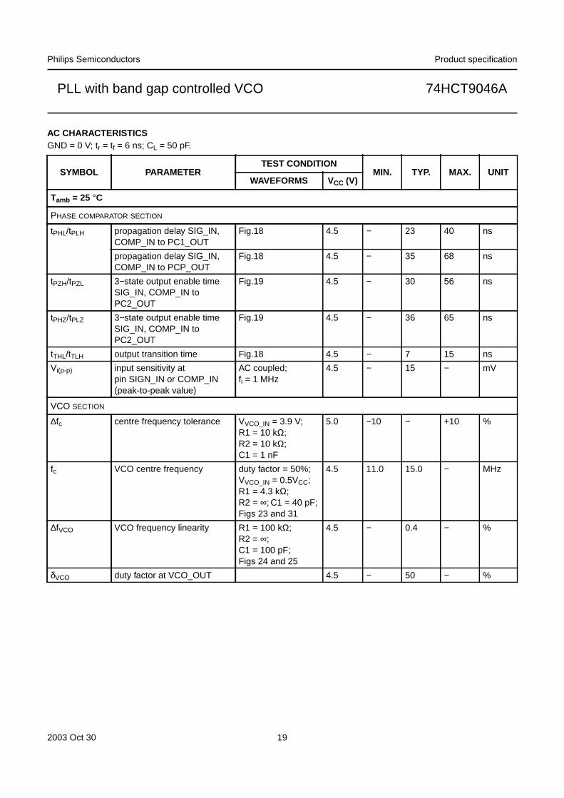
AC CHARACTERISTICSGND = 0 V; tr = tf = 6 ns; CL = 50 pF.
SYMBOL PARAMETERTEST CONDITION
MIN. TYP. MAX. UNITWAVEFORMS VCC (V)
Tamb = 25 °C
PHASE COMPARATOR SECTION
tPHL/tPLH propagation delay SIG_IN,COMP_IN to PC1_OUT
Fig.18 4.5 − 23 40 ns
propagation delay SIG_IN,COMP_IN to PCP_OUT
Fig.18 4.5 − 35 68 ns
tPZH/tPZL 3−state output enable timeSIG_IN, COMP_IN toPC2_OUT
Fig.19 4.5 − 30 56 ns
tPHZ/tPLZ 3−state output enable timeSIG_IN, COMP_IN toPC2_OUT
Fig.19 4.5 − 36 65 ns
tTHL/tTLH output transition time Fig.18 4.5 − 7 15 ns
Vi(p-p) input sensitivity atpin SIGN_IN or COMP_IN(peak-to-peak value)
AC coupled;fi = 1 MHz
4.5 − 15 − mV
VCO SECTION
∆fc centre frequency tolerance VVCO_IN = 3.9 V;R1 = 10 kΩ;R2 = 10 kΩ;C1 = 1 nF
5.0 −10 − +10 %
fc VCO centre frequency duty factor = 50%;VVCO_IN = 0.5VCC;R1 = 4.3 kΩ;R2 = ∞; C1 = 40 pF;Figs 23 and 31
4.5 11.0 15.0 − MHz
∆fVCO VCO frequency linearity R1 = 100 kΩ;R2 = ∞;C1 = 100 pF;Figs 24 and 25
4.5 − 0.4 − %
δVCO duty factor at VCO_OUT 4.5 − 50 − %
2003 Oct 30 20
Philips Semiconductors Product specification
PLL with band gap controlled VCO 74HCT9046A
Tamb = −40 to +85 °C
PHASE COMPARATOR SECTION
tPHL/tPLH propagation delay SIG_IN,COMP_IN to PC1_OUT
Fig.18 4.5 − − 50 ns
propagation delay SIG_IN,COMP_IN to PCP_OUT
Fig.18 4.5 − − 85 ns
tPZH/tPZL 3−state output enable timeSIG_IN, COMP_IN toPC2_OUT
Fig.19 4.5 − − 70 ns
tPHZ/tPLZ 3−state output enable timeSIG_IN, COMP_IN toPC2_OUT
Fig.19 4.5 − − 81 ns
tTHL/tTLH output transition time Fig.18 4.5 − − 19 ns
VCO SECTION
∆f/T frequency stability withtemperature change
VVCO_IN = 0.5VCC;recommendedrange: R1 = 10 kΩ;R2 = 10 kΩ;C1 = 1 nF;see Figs 20 to 22
4.5 0.06 − − %/K
Tamb = −40 to +125 °C
PHASE COMPARATOR SECTION
tPHL/tPLH propagation delay SIG_IN,COMP_IN to PC1_OUT
Fig.18 4.5 − − 60 ns
propagation delay SIG_IN,COMP_IN to PCP_OUT
Fig.18 4.5 − − 102 ns
tPZH/tPZL 3−state output enable timeSIG_IN, COMP_IN toPC2_OUT
Fig.19 4.5 − − 84 ns
tPHZ/tPLZ 3−state output enable timeSIG_IN, COMP_IN toPC2_OUT
Fig.19 4.5 − − 98 ns
tTHL/tTLH output transition time Fig.18 4.5 − − 22 ns
SYMBOL PARAMETERTEST CONDITION
MIN. TYP. MAX. UNITWAVEFORMS VCC (V)
2003 Oct 30 21
Philips Semiconductors Product specification
PLL with band gap controlled VCO 74HCT9046A
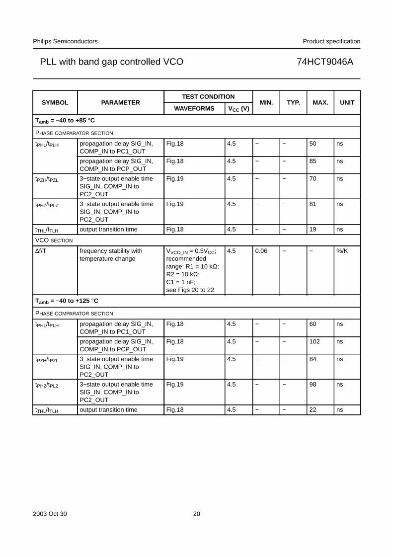
Fig.18 Waveforms showing input (SIG_IN and COMP_IN) to output (PCP_OUT and PC1_OUT) propagationdelays and the output transition times.
MBD106
t PHL
t THL
t PLH
t TLH
SIG_IN, COMP_INinputs
PCP_OUT, PC1_OUToutputs
VM
VM
VM = 0.5VCC; VI = GND to VCC.
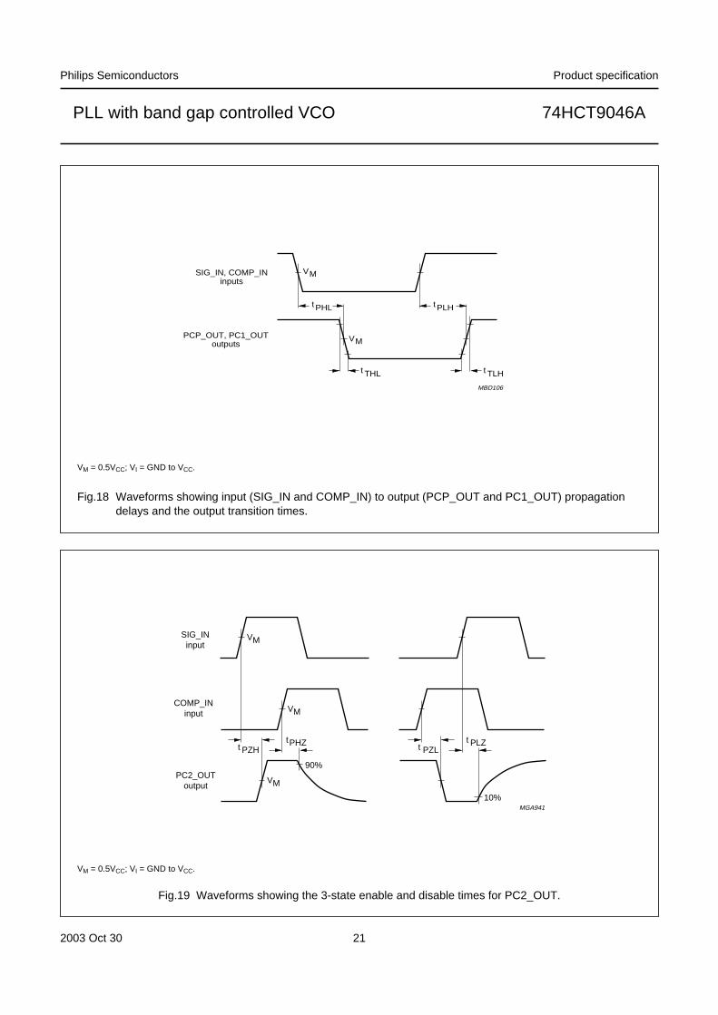
Fig.19 Waveforms showing the 3-state enable and disable times for PC2_OUT.
MGA941
t PLZt PZHtPHZ
10%
90%
t PZL
SIG_INinput
COMP_INinput
PC2_OUToutput
MV
MV
MV
VM = 0.5VCC; VI = GND to VCC.

2003 Oct 30 22
Philips Semiconductors Product specification
PLL with band gap controlled VCO 74HCT9046A
50 0 50 150
20
10
10
20
0
MBD115
100
∆ f(%)
5.5 V
4.5 V
V =CC
T ( C)ambo
Fig.20 Frequency stability of the VCO as a function of ambient temperature with supply voltage as a parameter.
MBD116
T ( C)amb
0
f(%)
o15010050050
15
10
5
5
10
15∆
5.5 V
4.5 V
V =CC
b. R1 = 10 kΩ; R2 = ∞; C1 = 100 pF.a. R1 = 3 kΩ; R2 = ∞; C1 = 100 pF.
50 0 50 150
10
5
5
10
0
MBD124
100
∆ f(%)
5.5 V
4.5 V
V =CC
T ( C)ambo
Fig.21 Frequency stability of the VCO as a function of ambient temperature with supply voltage as a parameter.
MBD117
T ( C)amb
0
f(%)
o15010050050
20
15
10
5
10
15∆
5.5 V
4.5 V
V =CC
5
b. R1 = ∞; R2 = 3 kΩ; C1 = 100 pF.a. R1 = 300 kΩ; R2 = ∞; C1 = 100 pF.

2003 Oct 30 23
Philips Semiconductors Product specification
PLL with band gap controlled VCO 74HCT9046A
MBD118
T ( C)amb
0
f(%)
o15010050050
12
8
4
4
8
∆
5.5 V
4.5 V
V =CC
Fig.22 Frequency stability of the VCO as a function of ambient temperature with supply voltage as a parameter.
MBD119
T ( C)amb
0
f(%)
o15010050050
10
5
5
10
∆
5.5 V
4.5 V
V =CC
b. R1 = ∞; R2 = 300 kΩ; C1 = 100 pF.a. R1 = ∞; R2 = 10 kΩ; C1 = 100 pF.
2003 Oct 30 24
Philips Semiconductors Product specification
PLL with band gap controlled VCO 74HCT9046A
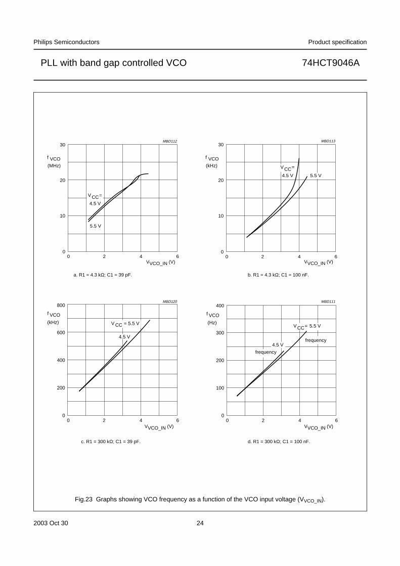
Fig.23 Graphs showing VCO frequency as a function of the VCO input voltage (VVCO_IN).
a. R1 = 4.3 kΩ; C1 = 39 pF. b. R1 = 4.3 kΩ; C1 = 100 nF.
c. R1 = 300 kΩ; C1 = 39 pF. d. R1 = 300 kΩ; C1 = 100 nF.
handbook, halfpage
0 2 4 6
800
600
200
0
400
MBD120
f VCO
(kHz) V = 5.5 VCC
4.5 V
VVCO_IN (V)
handbook, halfpage
0 2 4 6
400
300
100
0
200
MBD111
f VCO
(Hz)
frequency
frequency4.5 V
5.5 VV =CC
VVCO_IN (V)
0 2 4 6
30
10
0
20
MBD112
VVCO_IN (V)
f VCO(MHz)
5.5 V
4.5 V
V =CC
0 2 4 6
30
10
0
20
MBD113
f VCO(kHz)
5.5 V4.5 V
V =CC
VVCO_IN (V)
2003 Oct 30 25
Philips Semiconductors Product specification
PLL with band gap controlled VCO 74HCT9046A
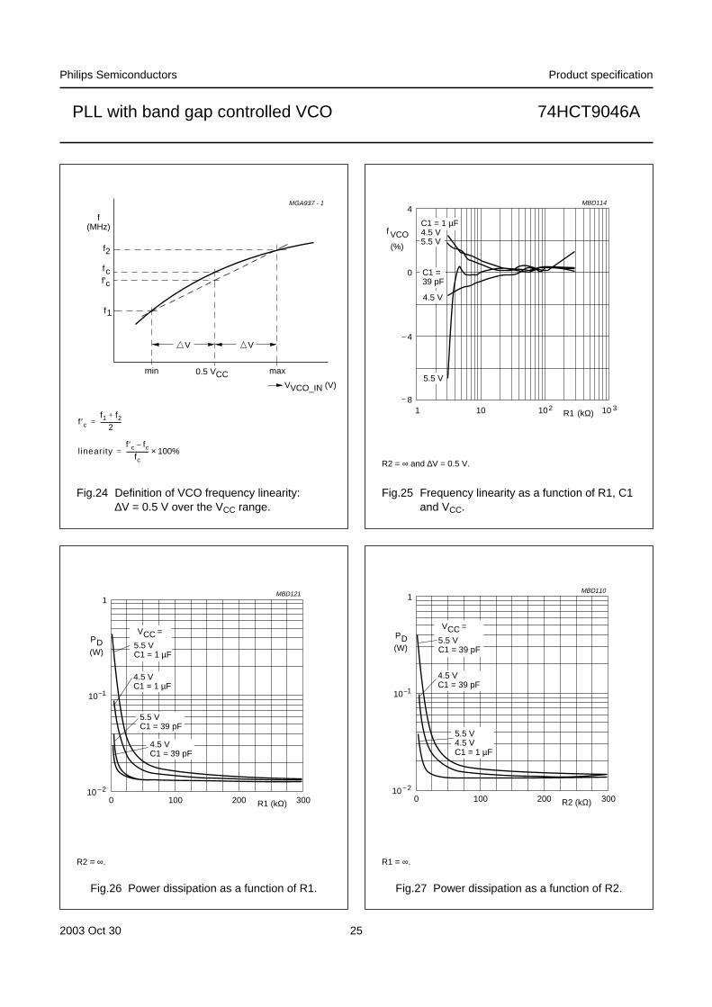
Fig.24 Definition of VCO frequency linearity:∆V = 0.5 V over the VCC range.
MGA937 - 1
f(MHz)
max
f1
min 0.5 VCC
f'c
fc
f2
VVCO_IN (V)
V V
f ′cf1 f2+
2---------------=
l inearityf ′c fc–
fc---------------- 100%×=
Fig.25 Frequency linearity as a function of R1, C1and VCC.
4
4
0
1
MBD114
10 102 10 38
f VCO(%)
R1 (kΩ)
C1 = 1 µF4.5 V5.5 V
C1 = 39 pF
4.5 V
5.5 V
R2 = ∞ and ∆V = 0.5 V.
Fig.26 Power dissipation as a function of R1.
3000 100
MBD121
10 1
1
20010 2
R1 (kΩ)
4.5 VC1 = 1 µF
5.5 VC1 = 39 pF
4.5 VC1 = 39 pF
5.5 VC1 = 1 µF
CCV =PD(W)
R2 = ∞.
Fig.27 Power dissipation as a function of R2.
R1 = ∞.
3000 100
MBD110
10 1
1
20010 2
R2 (kΩ)
P 5.5 VC1 = 39 pF
CC
5.5 V4.5 VC1 = 1 µF
4.5 VC1 = 39 pF
V =
D(W)
2003 Oct 30 26
Philips Semiconductors Product specification
PLL with band gap controlled VCO 74HCT9046A
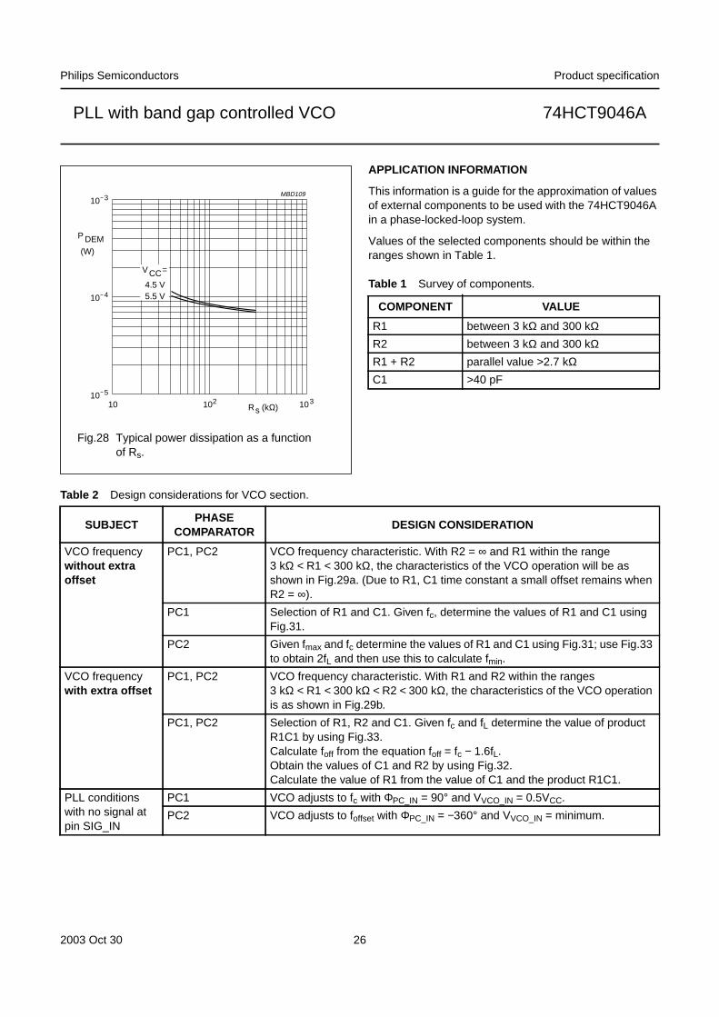
APPLICATION INFORMATION
This information is a guide for the approximation of valuesof external components to be used with the 74HCT9046Ain a phase-locked-loop system.
Values of the selected components should be within theranges shown in Table 1.
Table 1 Survey of components.
Fig.28 Typical power dissipation as a functionof Rs.
103
MBD109
10210
10 4
P DEM(W)
R (kΩ)s
V =CC
5.5 V4.5 V
10 5
10 3
COMPONENT VALUE
R1 between 3 kΩ and 300 kΩR2 between 3 kΩ and 300 kΩR1 + R2 parallel value >2.7 kΩC1 >40 pF
Table 2 Design considerations for VCO section.
SUBJECTPHASE
COMPARATORDESIGN CONSIDERATION
VCO frequencywithout extraoffset
PC1, PC2 VCO frequency characteristic. With R2 = ∞ and R1 within the range3 kΩ < R1 < 300 kΩ, the characteristics of the VCO operation will be asshown in Fig.29a. (Due to R1, C1 time constant a small offset remains whenR2 = ∞).
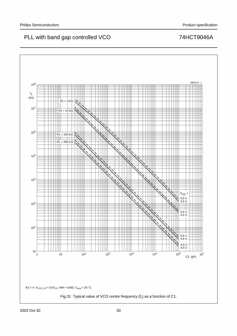
PC1 Selection of R1 and C1. Given fc, determine the values of R1 and C1 usingFig.31.
PC2 Given fmax and fc determine the values of R1 and C1 using Fig.31; use Fig.33to obtain 2fL and then use this to calculate fmin.
VCO frequencywith extra offset
PC1, PC2 VCO frequency characteristic. With R1 and R2 within the ranges3 kΩ < R1 < 300 kΩ < R2 < 300 kΩ, the characteristics of the VCO operationis as shown in Fig.29b.
PC1, PC2 Selection of R1, R2 and C1. Given fc and fL determine the value of productR1C1 by using Fig.33.Calculate foff from the equation foff = fc − 1.6fL.Obtain the values of C1 and R2 by using Fig.32.Calculate the value of R1 from the value of C1 and the product R1C1.
PLL conditionswith no signal atpin SIG_IN
PC1 VCO adjusts to fc with ΦPC_IN = 90° and VVCO_IN = 0.5VCC.
PC2 VCO adjusts to foffset with ΦPC_IN = −360° and VVCO_IN = minimum.
2003 Oct 30 27
Philips Semiconductors Product specification
PLL with band gap controlled VCO 74HCT9046A
MGA938
fVCO
fmax
fc
f min
1.1 V 0.5 VCC VCCVCC−1.1 V
VCO_IN
2fL due toR1,C1
0.6fL
foff
fVCO
fmax
fc
f min
1.1 V
VCO_IN
2fL due toR1,C1
due toR2,C1
MGA939
0.5 VCC VCCVCC−1.1 V
Fig.29 Frequency characteristic of VCO.
b. Operating with offset;fc = centre frequency;2fL = frequency lock range.
a. Operating without offset;fc = centre frequency;2fL = frequency lock range.
2003 Oct 30 28
Philips Semiconductors Product specification
PLL with band gap controlled VCO 74HCT9046A
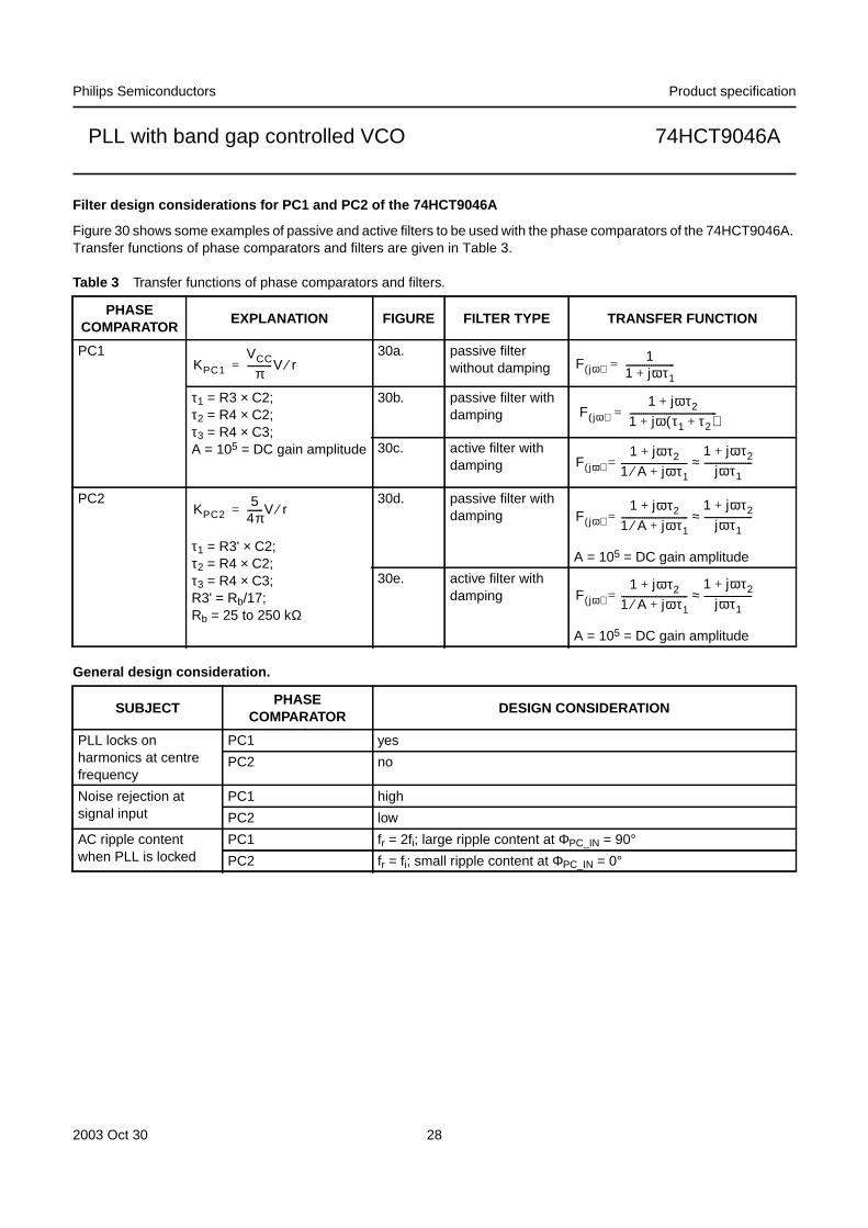
Filter design considerations for PC1 and PC2 of the 74HCT9046A
Figure 30 shows some examples of passive and active filters to be used with the phase comparators of the 74HCT9046A.Transfer functions of phase comparators and filters are given in Table 3.
Table 3 Transfer functions of phase comparators and filters.
General design consideration.
PHASECOMPARATOR
EXPLANATION FIGURE FILTER TYPE TRANSFER FUNCTION
PC1 30a. passive filterwithout damping
τ1 = R3 × C2;τ2 = R4 × C2;τ3 = R4 × C3;A = 105 = DC gain amplitude
30b. passive filter withdamping
30c. active filter withdamping
PC2
τ1 = R3' × C2;τ2 = R4 × C2;τ3 = R4 × C3;R3' = Rb/17;Rb = 25 to 250 kΩ
30d. passive filter withdamping
A = 105 = DC gain amplitude
30e. active filter withdamping
A = 105 = DC gain amplitude
SUBJECTPHASE
COMPARATORDESIGN CONSIDERATION
PLL locks onharmonics at centrefrequency
PC1 yes
PC2 no
Noise rejection atsignal input
PC1 high
PC2 low
AC ripple contentwhen PLL is locked
PC1 fr = 2fi; large ripple content at ΦPC_IN = 90°PC2 fr = fi; small ripple content at ΦPC_IN = 0°
KPC1
VCC
π-----------V r⁄= F jω( )1
1 jωτ1+---------------------=
F jω( )1 jωτ2+
1 jω τ1 τ2+( )+--------------------------------------=
F jω( )1 jωτ2+
1 A⁄ jωτ1+-----------------------------=
1 jωτ2+
jωτ1---------------------≈
KPC25
4π-------V r⁄= F jω( )1 jωτ2+
1 A⁄ jωτ1+-----------------------------=
1 jωτ2+
jωτ1---------------------≈
F jω( )1 jωτ2+
1 A⁄ jωτ1+-----------------------------=
1 jωτ2+
jωτ1---------------------≈

2003 Oct 30 29
Philips Semiconductors Product specification
PLL with band gap controlled VCO 74HCT9046A
MBD107 - 1
X1/ τ
R3
C2
F(jω)
R3
C2
C3 R4
C3
A
R4
C2
R3
R3'
C2
R4AR3'
A
C3
R4
C2
Oτ
X
2 1τ1 τ2
Oτ
X
2
1/ τ 2 1/ τ3
1/
Oτ
X
2
1/ Aτ1/
1
Oτ
X
2
1/ Aτ1/
1
A
1/ τ2 1/ τ3
1/ τ1A
A
1/ τ2 1/ τ3
τ 11/A
A
1/ τ2 1/ τ3
CIRCUITAMPLITUDE
CHARACTERISTICPOLE ZERODIAGRAM
1/ τ 1 1
τ1 τ21/
1/ τ1A
PC2
PC1
τ 11/AR3'
1/
F(jω)
Fig.30 Passive and active filters for 74HCT9046A.
a.
b.
c.
d.
e.
2003 Oct 30 30
Philips Semiconductors Product specification
PLL with band gap controlled VCO 74HCT9046A
Fig.31 Typical value of VCO centre frequency (fc) as a function of C1.
107105104103101
105
103
10
102
104
106
106
C1 (pF)
107
108
(Hz)
fc
102
MBD103 - 1
V =CC5.5 V4.5 V
ΩR1 = 3 k
R1 = 10 kΩ
R1 = 150 kΩ
R1 = 300 kΩ
5.5 V4.5 V
5.5 V4.5 V
5.5 V4.5 V
R2 = ∞; VVCO_IN = 0.5VCC; INH = GND; Tamb = 25 °C.

2003 Oct 30 31
Philips Semiconductors Product specification
PLL with band gap controlled VCO 74HCT9046A
Fig.32 Typical value of frequency offset as a function of C1.
107105104103101
105
103
10
102
104
106
106
C1 (pF)
107
108
(Hz)foff
102
MBD104
R2 = 150 kΩ
R2 = 300 kΩ
R2 = 3 kΩ
R2 = 10 kΩ
V =CC4.5 V - 5.5 V
4.5 V - 5.5 V
4.5 V - 5.5 V
4.5 V - 5.5 V
R1 = ∞; VVCO_IN = 0.5VCC; INH = GND; Tamb = 25 °C.
2003 Oct 30 32
Philips Semiconductors Product specification
PLL with band gap controlled VCO 74HCT9046A
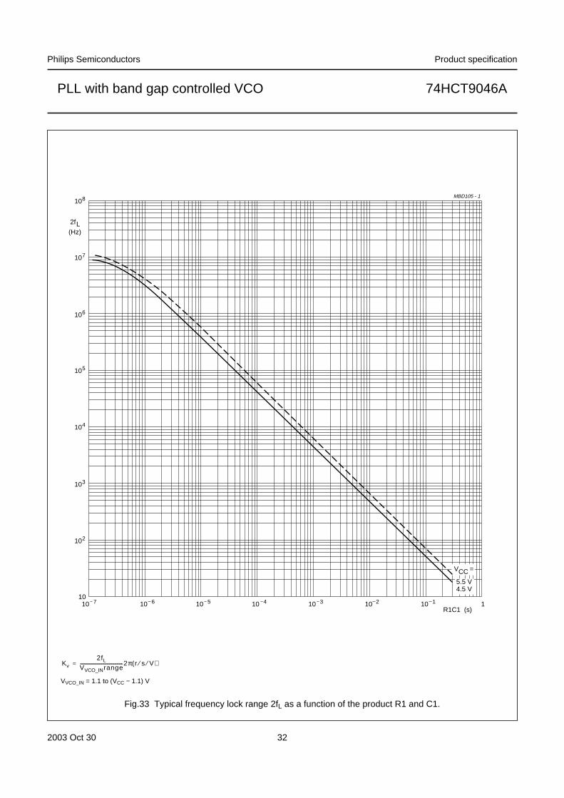
Fig.33 Typical frequency lock range 2fL as a function of the product R1 and C1.
VVCO_IN = 1.1 to (VCC − 1.1) V
Kv
2fLVVCO_INrange--------------------------------------2π r s⁄ V⁄( )=
10 7
105
103
10
102
104
106
R1C1 (s)
107
108
(Hz)
2fL
MBD105 - 1
V =CC
10 6 10 5 10 4 10 3 10 2 10 1 1
5.5 V4.5 V
2003 Oct 30 33
Philips Semiconductors Product specification
PLL with band gap controlled VCO 74HCT9046A
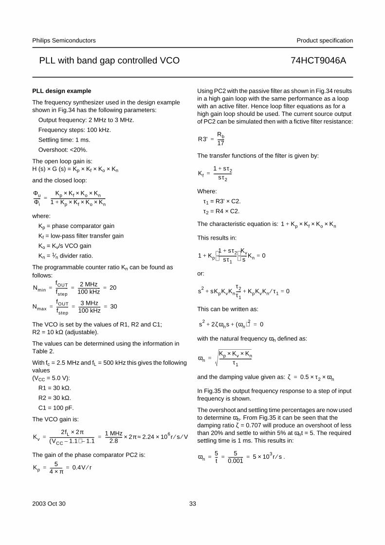
PLL design example
The frequency synthesizer used in the design exampleshown in Fig.34 has the following parameters:
Output frequency: 2 MHz to 3 MHz.
Frequency steps: 100 kHz.
Settling time: 1 ms.
Overshoot: <20%.
The open loop gain is:H (s) × G (s) = Kp × Kf × Ko × Kn
and the closed loop:
where:
Kp = phase comparator gain
Kf = low-pass filter transfer gain
Ko = Kv/s VCO gain
Kn = 1⁄n divider ratio.
The programmable counter ratio Kn can be found asfollows:
The VCO is set by the values of R1, R2 and C1;R2 = 10 kΩ (adjustable).
The values can be determined using the information inTable 2.
With fc = 2.5 MHz and fL = 500 kHz this gives the followingvalues(VCC = 5.0 V):
R1 = 30 kΩ.
R2 = 30 kΩ.
C1 = 100 pF.
The VCO gain is:
The gain of the phase comparator PC2 is:
Using PC2 with the passive filter as shown in Fig.34 resultsin a high gain loop with the same performance as a loopwith an active filter. Hence loop filter equations as for ahigh gain loop should be used. The current source outputof PC2 can be simulated then with a fictive filter resistance:
The transfer functions of the filter is given by:
Where:
τ1 = R3' × C2.
τ2 = R4 × C2.
The characteristic equation is:
This results in:
or:
This can be written as:
with the natural frequency ωn defined as:
and the damping value given as:
In Fig.35 the output frequency response to a step of inputfrequency is shown.
The overshoot and settling time percentages are now usedto determine ωn. From Fig.35 it can be seen that thedamping ratio ζ = 0.707 will produce an overshoot of lessthan 20% and settle to within 5% at ωnt = 5. The requiredsettling time is 1 ms. This results in:
.
Φu
Φi-------
Kp Kf× Ko× Kn×1 Kp Kf Ko× Kn××+------------------------------------------------------=
Nmin
fOUT
fstep------------
2 MHz100 kHz---------------------- 20= = =
Nmax
fOUT
fstep------------
3 MHz100 kHz---------------------- 30= = =
Kv
2fL 2π×VCC 1.1–( ) 1.1–
--------------------------------------------1 MHz
2.8----------------- 2π× 2.24 106× r s⁄ V⁄≈= =
Kp5
4 π×------------ 0.4V r⁄= =
R3'Rb
17-------=
Kf
1 sτ2+
sτ2------------------=
1 Kp Kf× Ko× Kn×+
1 Kp
1 sτ2+
sτ1------------------
Kv
s------Kn 0=+
s2 sKpKvKn
τ2
τ1----- KpKvKn τ1 0=⁄+ +
s2 2ζωns ωn( )2++ 0=
ωnKp Kv Kn××
τ1--------------------------------=
ζ 0.5 τ2 ωn××=
ωn5t---
50.001--------------- 5 103× r s⁄= = =
2003 Oct 30 34
Philips Semiconductors Product specification
PLL with band gap controlled VCO 74HCT9046A
Rewriting the equation for natural frequency results in:
The maximum overshoot occurs at Nmax = 30; hence Kn = 1⁄30:
When C2 = 470 nF, it follows:
Hence the current source bias resistance
Rb = 17 × 2550 = 43 kΩ.
With ζ = 0.707 (0.5 × τ2 × ωn) it follows:
For extra ripple suppression a capacitor C3 can be connected in parallel with R4, with an extra τ3 = R4 × C3.
For stability reasons τ3 should be <0.1τ2, hence C3 < 0.1C2 or C3 = 39 nF.
τ1
Kp Kv× Kn×
ωn( )2--------------------------------=
τ10.4 2.24× 106×
50002 30×------------------------------------------ 0.0012= =
R3 ′τ1
C2--------
0.0012
470 10 9–×---------------------------- 2550 Ω= = =
τ20.707
0.5 5000×---------------------------- 0.00028= =
R4τ2
C2--------
0.00028
470 10 9–×---------------------------- 600 Ω= = =
MBD098
R4
C2 R2R1
VCOR3'PHASE
COMPARATORPC2
DIVIDE BY 10"190"
OSCILLATOR"HCU04"
13100 kHz
14
3
4fOUT
PROGRAMMABLEDIVIDER
"4059"
9
11 12 6 7 5
1 MHz
Kp
Kn
Kf Ko
C1
C3
(1)
R
15
bΦu
Fig.34 Frequency synthesizer.
(1) R3' fictive resistance=
R3'Rb
17-------=
C1 = 100 pF.
C2 = 470 nF.
C3 = 39 nF.
R1 = 30 kΩ.
R2 = 30 kΩ.
R3' = 2550 Ω.
Rb = 43 kΩ.
R4 = 600 Ω.

2003 Oct 30 35
Philips Semiconductors Product specification
PLL with band gap controlled VCO 74HCT9046A
0 1 2 4
1.6
1.0
0.6
0
0.8
MGA959
3
1.4
1.2
0.4
0.2
5 6 7 8ω nt
∆ ω (t)e∆ ωe /ω n
∆ Φ (t)e∆ Φe /ω n
−0.6
0
0.4
1.0
0.2
−0.4
−0.2
0.6
0.8
= 5.0ζ
0.50.7071.0
= 0.3ζ
= 2.0ζ
Fig.35 Type 2, second order frequency step response.
Since the output frequency is proportional to the VCOcontrol voltage, the PLL frequency response can beobserved with an oscilloscope by monitoring pin VCO_INof the VCO. The average frequency response, ascalculated by the Laplace method, is found experimentallyby smoothing this voltage at pin VCO_IN with a simple RCfilter, whose time constant is long compared with thephase detector sampling rate but short compared with thePLL response time.
Further information
For an extensive description and application exampleplease refer to “Application note” ordering number9397 750 00078.
MGA9523.1
3.0
2.9
2.1
2.0
1.90 0.5 1.0 1.5 2.0 2.5
time (ms)
proportionalto outputfrequency
(MHz)
N = 30
N stepped from 29 to 30
step input
N stepped from 21 to 20
Fig.36 Frequency compared to the time response.
2003 Oct 30 36
Philips Semiconductors Product specification
PLL with band gap controlled VCO 74HCT9046A
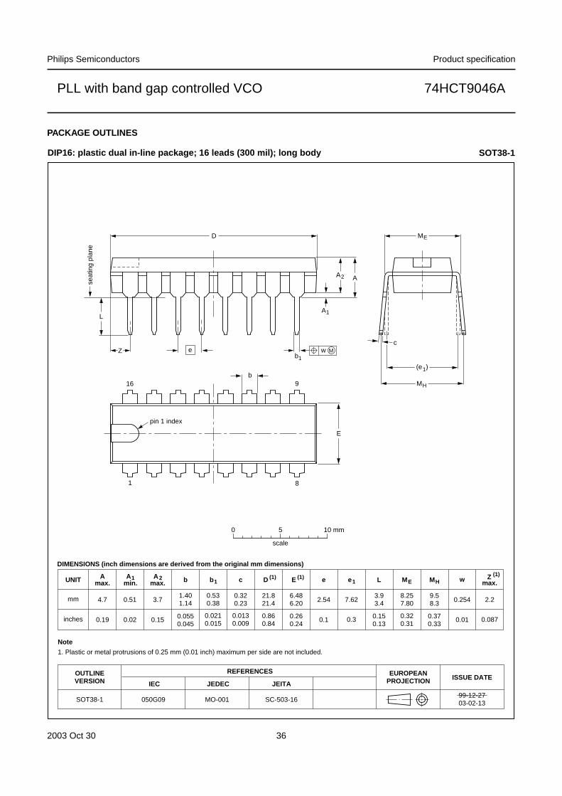
PACKAGE OUTLINES
UNIT Amax.
1 2 b1 c E e MHL
REFERENCESOUTLINEVERSION
EUROPEANPROJECTION ISSUE DATE
IEC JEDEC JEITA
mm
inches
DIMENSIONS (inch dimensions are derived from the original mm dimensions)
SOT38-199-12-2703-02-13
A min.
A max. b max.wMEe1
1.401.14
0.0550.045
0.530.38
0.320.23
21.821.4
0.860.84
6.486.20
0.260.24
3.93.4
0.150.13
0.2542.54 7.62
0.3
8.257.80
0.320.31
9.58.3
0.370.33
2.2
0.087
4.7 0.51 3.7
0.150.0210.015
0.0130.009 0.010.10.020.19
050G09 MO-001 SC-503-16
MH
c
(e )1
ME
A
L
seat
ing
plan
e
A1
w Mb1
e
D
A2
Z
16
1
9
8
b
E
pin 1 index
0 5 10 mm
scale
Note
1. Plastic or metal protrusions of 0.25 mm (0.01 inch) maximum per side are not included.
(1) (1)D(1)Z
DIP16: plastic dual in-line package; 16 leads (300 mil); long body SOT38-1

2003 Oct 30 37
Philips Semiconductors Product specification
PLL with band gap controlled VCO 74HCT9046A
X
w M
θ
AA1
A2
bp
D
HE
Lp
Q
detail X
E
Z
e
c
L
v M A
(A )3
A
8
9
1
16
y
pin 1 index
UNITA
max. A1 A2 A3 bp c D (1) E(1) (1)e HE L L p Q Zywv θ
REFERENCESOUTLINEVERSION
EUROPEANPROJECTION ISSUE DATE
IEC JEDEC JEITA
mm
inches
1.750.250.10
1.451.25 0.25
0.490.36
0.250.19
10.09.8
4.03.8
1.276.25.8
0.70.6
0.70.3 8
0
o
o
0.25 0.1
DIMENSIONS (inch dimensions are derived from the original mm dimensions)
Note
1. Plastic or metal protrusions of 0.15 mm (0.006 inch) maximum per side are not included.
1.00.4
SOT109-199-12-2703-02-19 076E07 MS-012
0.0690.0100.004
0.0570.049 0.01
0.0190.014
0.01000.0075
0.390.38
0.160.15
0.05
1.05
0.0410.2440.228
0.0280.020
0.0280.0120.01
0.25
0.01 0.0040.0390.016
0 2.5 5 mm
scale
SO16: plastic small outline package; 16 leads; body width 3.9 mm SOT109-1

2003 Oct 30 38
Philips Semiconductors Product specification
PLL with band gap controlled VCO 74HCT9046A
UNIT A1 A2 A3 bp c D (1) E (2) (1)e HE L L p Q Zywv θ
REFERENCESOUTLINEVERSION
EUROPEANPROJECTION ISSUE DATE
IEC JEDEC JEITA
mm 0.150.05
0.950.80
0.300.19
0.20.1
5.14.9
4.54.3 0.65
6.66.2
0.40.3
0.400.06
80
o
o0.13 0.10.21
DIMENSIONS (mm are the original dimensions)
Notes
1. Plastic or metal protrusions of 0.15 mm maximum per side are not included.
2. Plastic interlead protrusions of 0.25 mm maximum per side are not included.
0.750.50
SOT403-1 MO-15399-12-2703-02-18
w Mbp
D
Z
e
0.25
1 8
16 9
θ
AA1
A2
Lp
Q
detail X
L
(A )3
HE
E
c
v M A
XA
y
0 2.5 5 mm
scale
TSSOP16: plastic thin shrink small outline package; 16 leads; body width 4.4 mm SOT403-1
Amax.
1.1
pin 1 index

2003 Oct 30 39
Philips Semiconductors Product specification
PLL with band gap controlled VCO 74HCT9046A
DATA SHEET STATUS
Notes
1. Please consult the most recently issued data sheet before initiating or completing a design.
2. The product status of the device(s) described in this data sheet may have changed since this data sheet waspublished. The latest information is available on the Internet at URL http://www.semiconductors.philips.com.
3. For data sheets describing multiple type numbers, the highest-level product status determines the data sheet status.
LEVELDATA SHEET
STATUS(1)PRODUCT
STATUS(2)(3) DEFINITION
I Objective data Development This data sheet contains data from the objective specification for productdevelopment. Philips Semiconductors reserves the right to change thespecification in any manner without notice.
II Preliminary data Qualification This data sheet contains data from the preliminary specification.Supplementary data will be published at a later date. PhilipsSemiconductors reserves the right to change the specification withoutnotice, in order to improve the design and supply the best possibleproduct.
III Product data Production This data sheet contains data from the product specification. PhilipsSemiconductors reserves the right to make changes at any time in orderto improve the design, manufacturing and supply. Relevant changes willbe communicated via a Customer Product/Process Change Notification(CPCN).
DEFINITIONS
Short-form specification The data in a short-formspecification is extracted from a full data sheet with thesame type number and title. For detailed information seethe relevant data sheet or data handbook.
Limiting values definition Limiting values given are inaccordance with the Absolute Maximum Rating System(IEC 60134). Stress above one or more of the limitingvalues may cause permanent damage to the device.These are stress ratings only and operation of the deviceat these or at any other conditions above those given in theCharacteristics sections of the specification is not implied.Exposure to limiting values for extended periods mayaffect device reliability.
Application information Applications that aredescribed herein for any of these products are forillustrative purposes only. Philips Semiconductors makeno representation or warranty that such applications will besuitable for the specified use without further testing ormodification.
DISCLAIMERS
Life support applications These products are notdesigned for use in life support appliances, devices, orsystems where malfunction of these products canreasonably be expected to result in personal injury. PhilipsSemiconductors customers using or selling these productsfor use in such applications do so at their own risk andagree to fully indemnify Philips Semiconductors for anydamages resulting from such application.
Right to make changes Philips Semiconductorsreserves the right to make changes in the products -including circuits, standard cells, and/or software -described or contained herein in order to improve designand/or performance. When the product is in full production(status ‘Production’), relevant changes will becommunicated via a Customer Product/Process ChangeNotification (CPCN). Philips Semiconductors assumes noresponsibility or liability for the use of any of theseproducts, conveys no licence or title under any patent,copyright, or mask work right to these products, andmakes no representations or warranties that theseproducts are free from patent, copyright, or mask workright infringement, unless otherwise specified.

© Koninklijke Philips Electronics N.V. 2003 SCA75All rights are reserved. Reproduction in whole or in part is prohibited without the prior written consent of the copyright owner.
The information presented in this document does not form part of any quotation or contract, is believed to be accurate and reliable and may be changedwithout notice. No liability will be accepted by the publisher for any consequence of its use. Publication thereof does not convey nor imply any licenseunder patent- or other industrial or intellectual property rights.
Philips Semiconductors – a worldwide company
Contact information
For additional information please visit http://www.semiconductors.philips.com . Fax: +31 40 27 24825For sales offices addresses send e-mail to: [email protected] .
Printed in The Netherlands R44/05/pp40 Date of release: 2003 Oct 30 Document order number: 9397 750 12178
Related Documents