TRF3761 (TOP VIEW) GND AVDD_BIAS RBIAS1 GND VCTRL_IN AVDD_VCO AVDD_BUF AVDD_CAPARRAY GND AVDD PD_OUTBUF CHIP_EN CLOCK DATA STROBE DGND DGND DVDD1 AVDD_PRES GND DVDD2 MUX_OUT REF_IN GND AVDD_REF AVDD_CP CPOUT GND AVDD GND GND GND VCO_OUTP VCO_OUTM AVDD_OUTBUF GND AVDD_VCOBUF EXT_VCO_IN RBIAS2 GND 1 2 3 4 5 6 7 8 9 10 30 29 28 27 26 25 24 23 22 21 38 39 40 37 36 35 34 33 32 31 13 12 11 14 15 16 17 18 19 20 To Microcontroller To Microcontroller REF C4 1000 pF R3 2.37 kΩ C1 R1 C2 C3 R2 C6 10 pF C5 10 pF R5 120 Ω R6 120 Ω VDD VDD LOAD C7 1000 pF R4 4.75 kΩ Product Folder Sample & Buy Technical Documents Tools & Software Support & Community TRF3761, TRF3761-A, TRF3761-B TRF3761-C, TRF3761-D, TRF3761-E, TRF3761-F TRF3761-G, TRF3761-H, TRF3761-J, TRF3761-K SLWS181K – OCTOBER 2005 – REVISED DECEMBER 2015 TRF3761-x Integer-N PLL with Integrated VCO 1 Features 3 Description TRF3761 is a family of high performance, highly 1• Fully Integrated VCO integrated frequency synthesizers, optimized for high • Low Phase Noise: –137dBc/Hz (at 600kHz, f VCO performance applications. The TRF3761 includes a of 1.9GHz) low-noise, voltage-controlled oscillator (VCO) and an • Low Noise Floor: –158dBc/Hz at 10MHz Offset integer-N PLL. • Integer-N PLL TRF3761 integrates divide-by 1, 2, or 4 options for a • Input Reference Frequency range: 10MHz to more flexible output frequency range. It is controlled through a 3-wire serial-programming-interface (SPI) 104MHz interface. For power sensitive applications the • VCO Frequency Divided by 2-4 Output TRF3761 can be powered down by the SPI interface • Output Buffer Enable Pin or externally via chip_en pin 2. • Programmable Charge Pump Current Device Information (1) • Hardware and Software Power Down PART NUMBER PACKAGE BODY SIZE (NOM) • 3-Wire Serial Interface TRF3761 • Single Supply: 4.5V to 5.25V Operation VQFN (40) 6.00 mm x 6.00 mm TRF3761-x 2 Applications (1) For all available packages, see the orderable addendum at the end of the datasheet. • Wireless Infrastructure – WCDMA, CDMA, GSM – Wideband Transceivers – Wireless Local Loop – RFID Transceivers – Clock generation – IF LO generation Application Schematic 1 An IMPORTANT NOTICE at the end of this data sheet addresses availability, warranty, changes, use in safety-critical applications, intellectual property matters and other important disclaimers. PRODUCTION DATA.

Welcome message from author
This document is posted to help you gain knowledge. Please leave a comment to let me know what you think about it! Share it to your friends and learn new things together.
Transcript

TRF3761
(TOP VIEW)
GND
AVDD_BIAS
RBIAS1
GND
VCTRL_IN
AVDD_VCO
AVDD_BUF
AVDD_CAPARRAY
GND
AVDD
PD_OUTBUF
CHIP_EN
CLOCK
DATA
STROBE
DGND
DGND
DVDD1
AVDD_PRES
GND
DV
DD
2
MU
X_
OU
T
RE
F_
IN
GN
D
AV
DD
_R
EF
AV
DD
_C
P
CP
OU
T
GN
D
AV
DD
GN
D
GN
D
GN
D
VC
O_
OU
TP
VC
O_
OU
TM
AV
DD
_O
UT
BU
F
GN
D
AV
DD
_V
CO
BU
F
EX
T_
VC
O_
IN
RB
IAS
2
GN
D
1
2
3
4
5
6
7
8
9
10
30
29
28
27
26
25
24
23
22
21
383940 37 36 35 34 33 32 31
131211 14 15 16 17 18 19 20
To M
icro
contr
olle
r
To M
icro
contr
olle
r
RE
F
C41000 pF
R32.37 kΩ
C1R1
C2
C3
R2
C610 pF
C510 pF
R5120 Ω
R6120 Ω
VDDVDD
LOAD
C71000 pF
R44.75 kΩ
Product
Folder
Sample &Buy
Technical
Documents
Tools &
Software
Support &Community
TRF3761, TRF3761-A, TRF3761-BTRF3761-C, TRF3761-D, TRF3761-E, TRF3761-FTRF3761-G, TRF3761-H, TRF3761-J, TRF3761-K
SLWS181K –OCTOBER 2005–REVISED DECEMBER 2015
TRF3761-x Integer-N PLL with Integrated VCO1 Features 3 Description
TRF3761 is a family of high performance, highly1• Fully Integrated VCO
integrated frequency synthesizers, optimized for high• Low Phase Noise: –137dBc/Hz (at 600kHz, fVCO performance applications. The TRF3761 includes aof 1.9GHz) low-noise, voltage-controlled oscillator (VCO) and an
• Low Noise Floor: –158dBc/Hz at 10MHz Offset integer-N PLL.• Integer-N PLL TRF3761 integrates divide-by 1, 2, or 4 options for a• Input Reference Frequency range: 10MHz to more flexible output frequency range. It is controlled
through a 3-wire serial-programming-interface (SPI)104MHzinterface. For power sensitive applications the• VCO Frequency Divided by 2-4 OutputTRF3761 can be powered down by the SPI interface
• Output Buffer Enable Pin or externally via chip_en pin 2.• Programmable Charge Pump Current
Device Information(1)• Hardware and Software Power Down
PART NUMBER PACKAGE BODY SIZE (NOM)• 3-Wire Serial InterfaceTRF3761• Single Supply: 4.5V to 5.25V Operation VQFN (40) 6.00 mm x 6.00 mmTRF3761-x
2 Applications (1) For all available packages, see the orderable addendum atthe end of the datasheet.
• Wireless Infrastructure– WCDMA, CDMA, GSM– Wideband Transceivers– Wireless Local Loop– RFID Transceivers– Clock generation– IF LO generation
Application Schematic
1
An IMPORTANT NOTICE at the end of this data sheet addresses availability, warranty, changes, use in safety-critical applications,intellectual property matters and other important disclaimers. PRODUCTION DATA.

TRF3761, TRF3761-A, TRF3761-BTRF3761-C, TRF3761-D, TRF3761-E, TRF3761-FTRF3761-G, TRF3761-H, TRF3761-J, TRF3761-KSLWS181K –OCTOBER 2005–REVISED DECEMBER 2015 www.ti.com
Table of Contents1 Features .................................................................. 1 8 Detailed Description ............................................ 35
8.1 Overview ................................................................. 352 Applications ........................................................... 18.2 Functional Block Diagram ....................................... 353 Description ............................................................. 18.3 Feature Description................................................. 354 Revision History..................................................... 28.4 Device Functional Modes........................................ 375 Device Comparison Table ..................................... 38.5 Programming........................................................... 386 Pin Configuration and Functions ......................... 38.6 Register Maps ......................................................... 397 Specifications......................................................... 5 9 Application and Implementation ........................ 467.1 Absolute Maximum Ratings ...................................... 59.1 Application Information............................................ 467.2 Recommended Operating Conditions....................... 59.2 Typical Applications ................................................ 487.3 Thermal Information .................................................. 5
10 Power Supply Recommendations ..................... 547.4 Electrical Characteristics........................................... 611 Layout................................................................... 557.5 Electrical Characteristics, TRF3761-A ..................... 7
11.1 Layout Guidelines ................................................. 557.6 Electrical Characteristics,TRF3761-B ...................... 811.2 Layout Example .................................................... 557.7 Electrical Characteristics, TRF3761-C ..................... 9
12 Device and Documentation Support ................. 567.8 Electrical Characteristics, TRF3761-D ................... 1012.1 Related Links ........................................................ 567.9 Electrical Characteristics, TRF3761-E ................... 1112.2 Community Resources.......................................... 567.10 Electrical Characteristics, TRF3761-F ................. 1212.3 Trademarks ........................................................... 567.11 Electrical Characteristics, TRF3761-G ................. 1312.4 Electrostatic Discharge Caution............................ 567.12 Electrical Characteristics, TRF3761-H.................. 1412.5 Glossary ................................................................ 567.13 Electrical Characteristics, TRF3761-J .................. 15
13 Mechanical, Packaging, and Orderable7.14 Timing Requirements ............................................ 16Information ........................................................... 567.15 Typical Characteristics .......................................... 17
4 Revision HistoryNOTE: Page numbers for previous revisions may differ from page numbers in the current version.
Changes from Revision J (August 2009) to Revision K Page
• Added Pin Configuration and Functions section, ESD Rating table, Feature Description section, Device FunctionalModes, Application and Implementation section, Power Supply Recommendations section, Layout section, Deviceand Documentation Support section, and Mechanical, Packaging, and Orderable Information section .............................. 1
• Changed High-level input voltage MIN value From: 2.5 To: VCC - 2V ................................................................................... 6
Changes from Revision I (March 2008) to Revision J Page
• Changed Figure 2 ................................................................................................................................................................ 17• Changed Figure 3................................................................................................................................................................. 17• Changed Figure 4 ................................................................................................................................................................ 17• Changed Figure 5 ................................................................................................................................................................ 17• Changed Figure 6 ................................................................................................................................................................ 17• Changed Figure 7 ................................................................................................................................................................ 17• Changed Figure 8 ................................................................................................................................................................ 18• Changed Figure 9 ................................................................................................................................................................ 18• Changed Figure 10 .............................................................................................................................................................. 18
2 Submit Documentation Feedback Copyright © 2005–2015, Texas Instruments Incorporated
Product Folder Links: TRF3761 TRF3761-A TRF3761-B TRF3761-C TRF3761-D TRF3761-E TRF3761-F TRF3761-GTRF3761-H TRF3761-J TRF3761-K

GND
AVDD_BIAS
RBIAS1
GND
VCTRL_IN
AVDD_VCO
AVDD_BUF
AVDD_CAPARRAY
GND
AVDD
PD_OUTBUF
CHIP_EN
CLOCK
DATA
STROBE
DGND
DGND
DVDD1
AVDD_PRES
GND
DV
DD
2
MU
X_O
UT
RE
F_IN
GN
D
AV
DD
_R
EF
AV
DD
_C
P
CP
OU
T
GN
D
AV
DD
GN
D
GN
D
GN
D
VC
O_O
UT
P
VC
O_O
UT
M
AV
DD
_O
UT
BU
F
GN
D
AV
DD
_V
CO
BU
F
EX
T_V
CO
_IN
RB
IAS
2
GN
D
1
2
3
4
5
6
7
8
9
10
30
29
28
27
26
25
24
23
22
21
383940 37 36 35 34 33 32 31
131211 14 15 16 17 18 19 20
TRF3761, TRF3761-A, TRF3761-BTRF3761-C, TRF3761-D, TRF3761-E, TRF3761-FTRF3761-G, TRF3761-H, TRF3761-J, TRF3761-K
www.ti.com SLWS181K –OCTOBER 2005–REVISED DECEMBER 2015
5 Device Comparison Table
Div by 1 Div by 2 Div by 4PART NUMBER
Fstart Fstop Fstart Fstop Fstart Fstop
TRF3761-A 1493 1608 746.5 804 373.25 402
TRF3761-B 1595 1711 797.5 855.5 398.75 427.75
TRF3761-C 1660 1790 830 895 415 447.5
TRF3761-D 1740 1866 870 933 435 466.5
TRF3761-E 1805 1936 902.5 968 451.25 484
TRF3761-F 1850 1984 925 992 462.5 496
TRF3761-G 1920 2059 960 1029.5 480 514.75
TRF3761-H 2028 2175 1014 1087.5 507 543.75
TRF3761-J 2140 2295 1070 1147.5 535 573.75
6 Pin Configuration and Functions
RHA Package40-Pin VQFN
Top View
Copyright © 2005–2015, Texas Instruments Incorporated Submit Documentation Feedback 3
Product Folder Links: TRF3761 TRF3761-A TRF3761-B TRF3761-C TRF3761-D TRF3761-E TRF3761-F TRF3761-GTRF3761-H TRF3761-J TRF3761-K

TRF3761, TRF3761-A, TRF3761-BTRF3761-C, TRF3761-D, TRF3761-E, TRF3761-FTRF3761-G, TRF3761-H, TRF3761-J, TRF3761-KSLWS181K –OCTOBER 2005–REVISED DECEMBER 2015 www.ti.com
Pin FunctionsPIN (1)
I/O DESCRIPTIONNAME NO.
Once configured in register 1, this pin will control the output buffer. Logic level 0 turns on thePD_OUTBUF 1 I buffer and logic level 1 turns off the buffer.
This pin requires 4.5 to 5.25 V applied for normal operation. Grounding this pin will disable theCHIP_EN 2 I chip.
CLOCK 3 I Serial-programming-interface clock
DATA 4 I/O Serial-programming-interface data, used for programming the frequency and other features.
STROBE 5 I Serial-programming-interface strobe required to write the data to the chip
DGND 6, 7 Digital ground
Digital power supply, requires 4.5 to 5.25 V, Suggested decoupling, 0.1µF and 10pF capacitorsDVDD1 8 in parallel.
Power supply for prescaler circuit, requires 4.5 to 5.25 V, Suggested decoupling, 0.1uF andAVDD_PRES 9 10pF capacitors in parallel.
VCO output, can be used single ended matched to 50 ohms or in conjuction with VCO_OUTMVCO_OUTP 13 O (pin 14) with a balun.
VCO output, can be used single ended matched to 50 ohms or in conjunction with VCO_OUTPVCO_OUTM 14 O (pin 13) with a balun.
Power supply for output buffers, requires 4.5 to 5.25 V, Suggested decoupling, 0.1μF andAVDD_OUTBUF 15 10pF capacitors in parallel.
Power supply for VCO buffers, requires 4.5 to 5.25 V, Suggested decoupling, 0.1μF and 10pFAVDD_VCOBUF 17 capacitors in parallel.
EXT_VCO_IN 18 I External VCO input to prescaler, If using an external VCO instead of the internal VCO.
External bias resistor for setting the internal reference current requires a 4.75K ohm resister toRBIAS2 19 I/O ground.
Analog power supply, requires 4.5 to 5.25 V, Suggested decoupling, 0.1uF and 10μFAVDD 21 capacitors in parallel.
Power supply for VCO core and buffer, requires 4.5 to 5.25 V, Suggested decoupling, 0.1μFAVDD_CAPARRAY 23 and 10pF capacitors in parallel.
Power supply for VCO core and buffer, requires 4.5 to 5.25 V, Suggested decoupling, 0.1μFAVDD_BUF 24 and 10pF capacitors in parallel.
Power supply for VCO core and buffer, requires 4.5 to 5.25 V, Suggested decoupling, 0.1µFAVDD_VCO 25 and 10pF capacitors in parallel.
VCTRL_IN 26 I VCO control voltage, the output of the loop filter is applied to this pin.
External bias resistor for setting charge pump reference current, requires 2.37K ohm resistor toRBIAS1 28 I/O ground.
Power supply for band gap current bias, requires 4.5 to 5.25 V, Suggested decoupling, 0.1μFAVDD_BIAS 29 and 10pF capacitors in parallel.
10, 11, 12, 16, 20, 22,GND Analog ground27, 30, 31, 33, 37
Power supply for FUSE cell, requires 4.5 to 5.25 V. Suggested decoupling, 0.1μF, 1nF andAVDD 32 1pF capacitors in parallel.
CPOUT 34 O Charge pump output, connected to the input of loop filter.
Analog power supply for charge pump, requires 4.5 to 5.25 V, Suggested decoupling, 0.1μFAVDD_CP 35 and 10pF capacitors in parallel
Power supply for REF_IN circuitry, requires 4.5 to 5.25 V, Suggested decoupling, 0.1μF andAVDD_REF 36 10pF capacitors in parallel.
REF_IN 38 I Reference signal input, reference oscillator input of 10MHz to 104MHz.
Generally used for digital lock detect, can be used to verify locked condition by microcontroller,MUX_OUT 39 O high = locked, low = unlocked.
Power supply for the digital regulator, requires 4.5 to 5.25 V, Suggested decoupling, 0.1μF andDVDD2 40 10pF capacitors in parallel.
(1) Power Supply=VCC=(DVDD1, AVDD1, AVDD_PRES, AVDD_VCOBUF, AVDD, AVDD_CAPARRAY, AVDD_BUF, AVDD_VCO,AVDD_BIAS, AVDD_CP, AVDD_REF, DVDD2)
4 Submit Documentation Feedback Copyright © 2005–2015, Texas Instruments Incorporated
Product Folder Links: TRF3761 TRF3761-A TRF3761-B TRF3761-C TRF3761-D TRF3761-E TRF3761-F TRF3761-GTRF3761-H TRF3761-J TRF3761-K

TRF3761, TRF3761-A, TRF3761-BTRF3761-C, TRF3761-D, TRF3761-E, TRF3761-FTRF3761-G, TRF3761-H, TRF3761-J, TRF3761-K
www.ti.com SLWS181K –OCTOBER 2005–REVISED DECEMBER 2015
7 Specifications
7.1 Absolute Maximum Ratingsover operating free-air temperature range (unless otherwise noted) (1)
MIN MAX UNITSupply voltage range (2) –0.3 5.5 VDigital I/O voltage range –0.3 VCC +0.3 V
TJ Operating virtual junction temperature range –40 150 °CTstg Storage temperature –65 150 °C
(1) Stresses beyond those listed under Absolute Maximum Ratings may cause permanent damage to the device. These are stress ratingsonly, and functional operation of the device at these or any other conditions beyond those indicated under Recommended OperatingConditions is not implied. Exposure to absolute maximum rated conditions for extended periods may affect device reliability.
(2) All voltage values are with respect to network ground terminal.
7.2 Recommended Operating Conditionsover operating free-air temperature range (unless otherwise noted)
MIN NOM MAX UNITVCC Power supply voltage 4.5 5 5.25 V
Power supply voltage ripple 940 μVpp
TA Operating free air temperature range –40 85 °CTJ Operating virtual junction temperature range –40 150 °C
7.3 Thermal InformationTRF3761
THERMAL METRIC (1) RHA (VQFN) UNIT40 PINS
Soldered slug, no airflow 26 °C/WRθJA Junction-to-ambient thermal resistance Soldered slug, 200-LFM airflow 20.1 °C/W
Soldered slug, 400-LFM airflow 17.4 °C/WRθJC(top) Junction-to-case (top) thermal resistance 16.4 °C/WRθJB Junction-to-board thermal resistance 4.7 °C/WψJT Junction-to-top characterization parameter 0.2 °C/WψJB Junction-to-board characterization parameter 4.6 °C/WRθJC(bot) Junction-to-case (bottom) thermal resistance 1 °C/W
(1) For more information about traditional and new thermal metrics, see the Semiconductor and IC Package Thermal Metrics applicationreport, SPRA953.
Copyright © 2005–2015, Texas Instruments Incorporated Submit Documentation Feedback 5
Product Folder Links: TRF3761 TRF3761-A TRF3761-B TRF3761-C TRF3761-D TRF3761-E TRF3761-F TRF3761-GTRF3761-H TRF3761-J TRF3761-K

TRF3761, TRF3761-A, TRF3761-BTRF3761-C, TRF3761-D, TRF3761-E, TRF3761-FTRF3761-G, TRF3761-H, TRF3761-J, TRF3761-KSLWS181K –OCTOBER 2005–REVISED DECEMBER 2015 www.ti.com
7.4 Electrical CharacteristicsSupply voltage = VCC = 4.5 V to 5.25 V, TA = –40 to 85°C (unless otherwise noted)
PARAMETER TEST CONDITIONS MIN TYP MAX UNITDC PARAMETERS
Divide by 1 output 130 mAICC Total supply current TA = 25°C Divide by 2 output 140 mA
Divide by 4 output 150 mAREFERENCE OSCILLATOR PARAMETERSfref Reference frequency 10 104 MHz
Reference input sensitivity (REF_IN) 0.2 2.5 VPP
Parallel capacitance 5 6.52 pFReference input impedance (REF_IN)
Parallel resistance 3913 ΩPFD CHARGE PUMP
PFD frequency 30 MHzCharge pump current (ICP_OUT ) SPI programmable 5.6 mA
DIGITAL INTERFACE (PD_OUTBUF, CHIP_EN, CLOCK, DATA, STROBE)VIH High-level input voltage VCC - 2 VCC VVIL Low-level input voltage 0 0.8 VVOH High-level output voltage 0.8VCC VVOL Low-level output voltage 0.2VCC VOUTPUT POWER
Single ended 0 dBmDifferential 3 dBm
6 Submit Documentation Feedback Copyright © 2005–2015, Texas Instruments Incorporated
Product Folder Links: TRF3761 TRF3761-A TRF3761-B TRF3761-C TRF3761-D TRF3761-E TRF3761-F TRF3761-GTRF3761-H TRF3761-J TRF3761-K

TRF3761, TRF3761-A, TRF3761-BTRF3761-C, TRF3761-D, TRF3761-E, TRF3761-FTRF3761-G, TRF3761-H, TRF3761-J, TRF3761-K
www.ti.com SLWS181K –OCTOBER 2005–REVISED DECEMBER 2015
7.5 Electrical Characteristics, TRF3761-ASupply voltage = VCC = 5 V, TA = –40 to 85°C (unless otherwise noted)
PARAMETER TEST CONDITIONS MIN TYP MAX UNITNOISE CHARACTERISTICS
100kHz offset –116.7600kHz offset –136
VCO phase noise, fVCO = 1554MHz, 1MHz offset -141.6 dBc/HzFree running VCO direct output fO = 1554MHz6MHz offset –156.110MHz offset -158.1100kHz offset -122.8600kHz offset –142.7
VCO phase noise, fVCO = 1554MHz, 1MHz offset –147.5 dBc/HzFree running VCO divide-by-2 output fO = 777MHz6MHz offset –15710MHz offset –158.1100kHz offset –127.7600kHz offset -148.4
VCO phase noise, fVCO = 1554MHz, 1MHz offset -151.8 dBc/HzFree running VCO divide-by-4 output fO = 388.5MHz6MHz offset –156.310MHz offset –155.91kHz offset –83.4600kHz offset –135VCO phase noise, fVCO = 1554MHz, dBc/HzClosed loop phase noise direct output (1) (2) (3) fO = 1554MHz 1MHz offset –140.210MHz offset –158.2
RMS phase error 100Hz to 10MHz 0.95°Closed loop phase noise direct output(3)
1kHz offset –90.4VCO phase noise, 600kHz offset –141fVCO = 1554MHz,Closed loop phase noise divide-by-2 output (1) (2) dBc/HzfO = 777MHz 1MHz offset –146.2(3)
10MHz offset –158.25RMS phase error 100Hz to 10MHz 0.63°Closed loop phase noise divide-by-2 output (3)
1kHz offset -95VCO phase noise, 600kHz offset –147fVCO = 1554MHz,Closed loop phase noise divide-by-4 output (1) (2) dBc/HzfO = 388.5MHz 1MHz offset –151(3)
10MHz offset –156RMS phase error 100Hz to 10MHz 0.39°Closed loop phase noise divide-by-4 output (3)
VCO gain, Kv VCO free running 23 MHz/VReference spur (2) –80 dBc
(1) See Application Circuit Figure 87.(2) PFD = 200kHz, Loop Filter BW = 15kHz, Output frequency step = 200kHz.(3) Reference oscillator RMS phase error = 0.008250°, RMS jitter = 881.764 fs.
Copyright © 2005–2015, Texas Instruments Incorporated Submit Documentation Feedback 7
Product Folder Links: TRF3761 TRF3761-A TRF3761-B TRF3761-C TRF3761-D TRF3761-E TRF3761-F TRF3761-GTRF3761-H TRF3761-J TRF3761-K
TRF3761, TRF3761-A, TRF3761-BTRF3761-C, TRF3761-D, TRF3761-E, TRF3761-FTRF3761-G, TRF3761-H, TRF3761-J, TRF3761-KSLWS181K –OCTOBER 2005–REVISED DECEMBER 2015 www.ti.com
7.6 Electrical Characteristics,TRF3761-BSupply voltage = VCC = 5 V, TA = –40 to 85°C (unless otherwise noted)
PARAMETER TEST CONDITIONS MIN TYP MAX UNITNOISE CHARACTERISTICS
100kHz offset –119.34600kHz offset –139
VCO phase noise, fVCO = 1651MHz, 1MHz offset -142.1 dBc/HzFree running VCO direct output fO = 1651MHz6MHz offset –156.610MHz offset -158.6100kHz offset -127.8600kHz offset –146.5
VCO phase noise, fVCO = 1651MHz, 1MHz offset –149 dBc/HzFree running VCO divide-by-2 output fO = 825.5 MHz6MHz offset –156.210MHz offset –158.4100kHz offset –127.3600kHz offset -151.4
VCO phase noise, fVCO = 1651MHz, 1MHz offset -153 dBc/HzFree running VCO divide-by-4 output fO = 412.75 MHz6MHz offset –155.510MHz offset –155.91kHz offset –83.5600kHz offset –138VCO phase noise, fVCO = 1651MHz, dBc/HzClosed loop phase noise direct output (1) (2) (3) fO = 1651MHz 1MHz offset –141.810MHz offset –158.2
RMS phase error 100Hz to 10MHz 0.85°Closed loop phase noise direct output(3)
1kHz offset –90.2VCO phase noise, 600kHz offset –146fVCO = 1651MHz,Closed loop phase noise divide-by-2 output (1) (2) dBc/HzfO = 825.5 MHz 1MHz offset –147.39(3)
10MHz offset –158.25RMS phase error 100Hz to 10MHz 0.53°Closed loop phase noise divide-by-2 output (3)
1kHz offset -95.7VCO phase noise, 600kHz offset –151fVCO = 1651MHz,Closed loop phase noise divide-by-4 output (1) (2) dBc/HzfO = 412.75 MHz 1MHz offset –154(3)
10MHz offset –156RMS phase error 100Hz to 10MHz 0.33°Closed loop phase noise divide-by-4 output (3)
VCO gain, Kv VCO free running 23 MHz/VReference spur (2) –80 dBc
(1) See Application Circuit Figure 87.(2) PFD = 200kHz, Loop Filter BW = 15kHz, Output frequency step = 200kHz.(3) Reference oscillator RMS phase error = 0.008250°, RMS jitter = 881.764 fs.
8 Submit Documentation Feedback Copyright © 2005–2015, Texas Instruments Incorporated
Product Folder Links: TRF3761 TRF3761-A TRF3761-B TRF3761-C TRF3761-D TRF3761-E TRF3761-F TRF3761-GTRF3761-H TRF3761-J TRF3761-K

TRF3761, TRF3761-A, TRF3761-BTRF3761-C, TRF3761-D, TRF3761-E, TRF3761-FTRF3761-G, TRF3761-H, TRF3761-J, TRF3761-K
www.ti.com SLWS181K –OCTOBER 2005–REVISED DECEMBER 2015
7.7 Electrical Characteristics, TRF3761-CSupply voltage = VCC = 5 V, TA = –40 to 85°C (unless otherwise noted)
PARAMETER TEST CONDITIONS MIN TYP MAX UNITNOISE CHARACTERISTICS
100kHz offset –119.5600kHz offset –138.8
VCO phase noise, fVCO = 1723MHz, 1MHz offset -143.9 dBc/HzFree running VCO direct output fO = 1700MHz6MHz offset –155.310MHz offset –157.5100kHz offset –126600kHz offset –145.2
VCO phase noise, fVCO = 1723MHz, 1MHz offset –149.5 dBc/HzFree running VCO divide-by-2 output fO = 861.5 MHz6MHz offset –157.210MHz offset –158100kHz offset –133600kHz offset -151
VCO phase noise, fVCO = 1723MHz, 1MHz offset -153.8 dBc/HzFree running VCO divide-by-4 output fO = 430.75 MHz6MHz offset –15610MHz offset –156.51kHz offset –85600kHz offset –138.34VCO phase noise, fVCO = 1723MHz, dBc/HzClosed loop phase noise direct output (1) (2) (3) fO = 1723MHz, 1MHz offset –142.6810MHz offset –157.3
RMS phase error 100Hz to 10MHz 0.87°Closed loop phase noise direct output (3)
1kHz offset –90.1600kHz offset –145VCO phase noise, fVCO = 1723MHz, dBc/HzClosed loop phase noise divide-by-2 output (1) (2) (3) fO = 861.5 MHz 1MHz offset –148.610MHz offset –158
RMS phase error 100Hz to 10MHz 0.53°Closed loop phase noise divide-by-2 output (3)
1kHz offset –96.2600kHz offset –151VCO phase noise, fVCO = 1723MHz, dBc/HzClosed loop phase noise divide-by-4 output (1) (2) (3) fO = 430.75 MHz 1MHz offset –15310MHz offset –156
RMS phase error 100Hz to 10MHz 0.33°Closed loop phase noise divide-by-4 output (3)
VCO gain, Kv VCO free running 23 MHz/VReference spur (2) –80 dBc
(1) See Application Circuit Figure 87.(2) PFD = 200kHz, Loop Filter BW = 15kHz, Output frequency step = 200kHz.(3) Reference oscillator RMS phase error = 0.008250°, RMS jitter = 881.764 fs.
Copyright © 2005–2015, Texas Instruments Incorporated Submit Documentation Feedback 9
Product Folder Links: TRF3761 TRF3761-A TRF3761-B TRF3761-C TRF3761-D TRF3761-E TRF3761-F TRF3761-GTRF3761-H TRF3761-J TRF3761-K

TRF3761, TRF3761-A, TRF3761-BTRF3761-C, TRF3761-D, TRF3761-E, TRF3761-FTRF3761-G, TRF3761-H, TRF3761-J, TRF3761-KSLWS181K –OCTOBER 2005–REVISED DECEMBER 2015 www.ti.com
7.8 Electrical Characteristics, TRF3761-DSupply voltage = VCC = 5 V, TA = –40 to 85°C (unless otherwise noted)
PARAMETER TEST CONDITIONS MIN TYP MAX UNITNOISE CHARACTERISTICS
100kHz offset –118600kHz offset –138.5
VCO phase noise, fVCO = 1817MHz, 1MHz offset -144 dBc/HzFree running VCO direct output fO = 1817MHz6MHz offset –15610MHz offset –158100kHz offset –124.8600kHz offset –145.2
VCO phase noise, fVCO = 1817MHz, 1MHz offset –148 dBc/HzFree running VCO divide-by-2 output fO = 908.5MHz6MHz offset –157.810MHz offset –158.2100kHz offset –132600kHz offset -151
VCO phase noise, fVCO = 1817MHz, 1MHz offset -154 dBc/HzFree running VCO divide-by-4 output fO = 454.25MHz6MHz offset –15710MHz offset –157.51kHz offset –85600kHz offset –139VCO phase noise, fVCO = 1817MHz, dBc/HzClosed loop phase noise direct output (1) (2) (1) fO = 1817MHz 1MHz offset –14410MHz offset –159
RMS phase error 100Hz to 10MHz 0.85°Closed loop phase noise direct output (3)
1kHz offset –91VCO phase noise, 600kHz offset –146fVCO = 1817MHz,Closed loop phase noise divide-by-2 output (1) dBc/HzfO = 908.5MHz 1MHz offset –149(2) (3)
10MHz offset –159RMS phase error 100Hz to 10MHz 0.47°Closed loop phase noise divide-by-2 output (3)
1kHz offset –97VCO phase noise, 600kHz offset –151fVCO = 1817MHz,Closed loop phase noise divide-by-4 output (1) dBc/HzfO = 454.25MHz 1MHz offset –154(2) (3)
10MHz offset –157RMS phase error 100Hz to 10MHz 0.34°Closed loop phase noise divide-by-4 output (3)
VCO gain, Kv VCO free running 23 MHz/VReference spur (2) –80 dBc
(1) See Application Circuit Figure 87.(2) PFD = 200kHz, Loop Filter BW = 15kHz, Output frequency step = 200kHz.(3) Reference oscillator RMS phase error = 0.008250°, RMS jitter = 881.764 fs.
10 Submit Documentation Feedback Copyright © 2005–2015, Texas Instruments Incorporated
Product Folder Links: TRF3761 TRF3761-A TRF3761-B TRF3761-C TRF3761-D TRF3761-E TRF3761-F TRF3761-GTRF3761-H TRF3761-J TRF3761-K

TRF3761, TRF3761-A, TRF3761-BTRF3761-C, TRF3761-D, TRF3761-E, TRF3761-FTRF3761-G, TRF3761-H, TRF3761-J, TRF3761-K
www.ti.com SLWS181K –OCTOBER 2005–REVISED DECEMBER 2015
7.9 Electrical Characteristics, TRF3761-ESupply voltage = VCC = 5 V, TA = –40 to 85°C (unless otherwise noted)
PARAMETER TEST CONDITIONS MIN TYP MAX UNITNOISE CHARACTERISTICS
100kHz offset –118600kHz offset –138
VCO phase noise, fVCO = 1869MHz, 1MHz offset –142 dBc/HzFree running VCO direct output fO = 1869MHz6MHz offset –15510MHz offset –157.3100kHz offset –126600kHz offset –144
VCO phase noise, fVCO = 1869MHz, 1MHz offset –149 dBc/HzFree running VCO divide-by-2 output fO = 934.5MHz6MHz offset –15810MHz offset –158.2100kHz offset –132600kHz offset –150
VCO phase noise, fVCO = 1869MHz, 1MHz offset –154 dBc/HzFree running VCO divide-by-4 output fO = 467.25MHz6MHz offset -15710MHz offset –157.31kHz offset –84.5600kHz offset –140VCO phase noise, fVCO = 1869MHz, dBc/HzClosed loop phase noise direct output (1) (2) (3) fO = 1869MHz 1MHz offset –143.610MHz offset –157
RMS phase error 100Hz to 10MHz 0.9°Closed loop phase noise direct output (3)
1kHz offset –90.7600kHz offset –144VCO phase noise, fVCO = 1869MHz, dBc/HzClosed loop phase noise divide-by-2 output (1) (2) (3) fO = 934.5MHz 1MHz offset –148.510MHz offset –158
RMS phase error 100Hz to 10MHz 0.53°Closed loop phase noise divide-by-2 output (3)
1kHz offset –95600kHz offset –150VCO phase noise, fVCO = 1869MHz, dBc/HzClosed loop phase noise divide-by-4 output (1) (2) (3) fO = 467.25MHz 1MHz offset –15410MHz offset –157
RMS phase error 100Hz to 10MHz 0.35°Closed loop phase noise divide-by-4 output (3)
VCO gain, Kv VCO free running 23 MHz/VReference spur (2) –80 dBc
(1) See Application Circuit Figure 87.(2) PFD = 200kHz, Loop Filter BW = 15kHz, Output frequency step = 200kHz.(3) Reference oscillator RMS phase error = 0.008250°, RMS jitter = 881.764 fs.
Copyright © 2005–2015, Texas Instruments Incorporated Submit Documentation Feedback 11
Product Folder Links: TRF3761 TRF3761-A TRF3761-B TRF3761-C TRF3761-D TRF3761-E TRF3761-F TRF3761-GTRF3761-H TRF3761-J TRF3761-K

TRF3761, TRF3761-A, TRF3761-BTRF3761-C, TRF3761-D, TRF3761-E, TRF3761-FTRF3761-G, TRF3761-H, TRF3761-J, TRF3761-KSLWS181K –OCTOBER 2005–REVISED DECEMBER 2015 www.ti.com
7.10 Electrical Characteristics, TRF3761-FSupply voltage = VCC = 5 V, TA = –40 to 85°C (unless otherwise noted)
PARAMETER TEST CONDITIONS MIN TYP MAX UNITNOISE CHARACTERISTICS
100kHz offset -116600kHz offset -137
VCO phase noise, fVCO = 1916MHz, 1MHz offset -141 dBc/HzFree running VCO direct output fO = 1916MHz6MHz offset -15510MHz offset -157100kHz offset -113600kHz offset -136
VCO phase noise, fVCO = 1916MHz, 1MHz offset -147.5 dBc/HzFree running VCO divide-by-2 output fO = 958MHz6MHz offset -15510MHz offset -157.5100kHz offset -128600kHz offset -148
VCO phase noise, fVCO = 1916MHz, 1MHz offset -150 dBc/HzFree running VCO divide-by-4 output fO = 479MHz6MHz offset -15510MHz offset -1561kHz offset -82.5600kHz offset -136.7VCO phase noise, fVCO = 1916MHz, dBc/HzClosed loop phase noise direct output (1) (2) (3) fO = 1916MHz 1MHz offset -14210MHz offset -157
RMS phase error 100Hz to 10MHz 0.947°Closed loop phase noise direct output (3)
1kHz offset -88.6600kHz offset -142.6VCO phase noise, fVCO = 1916MHz, dBc/HzClosed loop phase noise divide-by-2 output (1) (2) (3) fO = 958MHz 1MHz offset -148.210MHz offset -158
RMS phase error 100Hz to 10MHz 0.477°Closed loop phase noise divide-by-2 output (3)
1kHz offset -95600kHz offset -148VCO phase noise, fVCO = 1916MHz, dBc/HzClosed loop phase noise divide-by-4 output (1) (2) (3) fO = 479MHz 1MHz offset -15210MHz offset -156
RMS phase error 100Hz to 10MHz 0.231°Closed loop phase noise divide-by-4 output (3)
VCO gain, Kv VCO free running 23 MHz/VReference spur (2) –80 dBc
(1) See Application Circuit Figure 87.(2) PFD = 200kHz, Loop Filter BW = 15kHz, Output frequency step = 200kHz.(3) Reference oscillator RMS phase error = 0.008250°, RMS jitter = 881.764 fs.
12 Submit Documentation Feedback Copyright © 2005–2015, Texas Instruments Incorporated
Product Folder Links: TRF3761 TRF3761-A TRF3761-B TRF3761-C TRF3761-D TRF3761-E TRF3761-F TRF3761-GTRF3761-H TRF3761-J TRF3761-K

TRF3761, TRF3761-A, TRF3761-BTRF3761-C, TRF3761-D, TRF3761-E, TRF3761-FTRF3761-G, TRF3761-H, TRF3761-J, TRF3761-K
www.ti.com SLWS181K –OCTOBER 2005–REVISED DECEMBER 2015
7.11 Electrical Characteristics, TRF3761-GSupply voltage = VCC = 5 V, TA = –40 to 85°C (unless otherwise noted)
PARAMETER TEST CONDITIONS MIN TYP MAX UNITNOISE CHARACTERISTICS
100kHz offset -115600kHz offset -136
VCO phase noise, fVCO = 1989MHz, 1MHz offset -141.2 dBc/HzFree running VCO direct output fO = 1989MHz6MHz offset -155.610MHz offset -159100kHz offset -121.3600kHz offset -142.4
VCO phase noise, fVCO = 1989MHz, 1MHz offset -141.5 dBc/HzFree running VCO divide-by-2 output fO = 994.5MHz6MHz offset -157.210MHz offset -158100kHz offset -128600kHz offset -148
VCO phase noise, fVCO = 1989MHz, 1MHz offset -151 dBc/HzFree running VCO divide-by-4 output fO = 497.25MHz6MHz offset -156.810MHz offset -1571kHz offset -83600kHz offset -136VCO phase noise, fVCO = 1989MHz, dBc/HzClosed loop phase noise direct output (1) (2) (3) fO = 1989MHz 1MHz offset -14110MHz offset -159
RMS phase error 100Hz to 10MHz 1°Closed loop phase noise direct output (3)
1kHz offset -88.7600kHz offset -141.9VCO phase noise, fVCO = 1989MHz, dBc/HzClosed loop phase noise divide-by-2 output (1) (2) (3) fO = 994.5MHz 1MHz offset -147.510MHz offset -158
RMS phase error 100Hz to 10MHz 0.509°Closed loop phase noise divide-by-2 output (3)
1kHz offset -95600kHz offset -147.9VCO phase noise, fVCO = 1989MHz, dBc/HzClosed loop phase noise divide-by-4 output (1) (2) (3) fO = 497.25MHz 1MHz offset -151.310MHz offset -156
RMS phase error 100Hz to 10MHz 0.252°Closed loop phase noise divide-by-4 output (3)
VCO gain, Kv VCO free running 23 MHz/VReference spur (2) –80 dBc
(1) See Application Circuit Figure 87.(2) PFD = 200kHz, Loop Filter BW = 15kHz, Output frequency step = 200kHz.(3) Reference oscillator RMS phase error = 0.008250°, RMS jitter = 881.764 fs.
Copyright © 2005–2015, Texas Instruments Incorporated Submit Documentation Feedback 13
Product Folder Links: TRF3761 TRF3761-A TRF3761-B TRF3761-C TRF3761-D TRF3761-E TRF3761-F TRF3761-GTRF3761-H TRF3761-J TRF3761-K

TRF3761, TRF3761-A, TRF3761-BTRF3761-C, TRF3761-D, TRF3761-E, TRF3761-FTRF3761-G, TRF3761-H, TRF3761-J, TRF3761-KSLWS181K –OCTOBER 2005–REVISED DECEMBER 2015 www.ti.com
7.12 Electrical Characteristics, TRF3761-HSupply voltage = VCC = 5 V, TA = –40 to 85°C (unless otherwise noted)
PARAMETER TEST CONDITIONS MIN TYP MAX UNITNOISE CHARACTERISTICS
100kHz offset –116600kHz offset –136
VCO phase noise, fVCO = 2116MHz, 1MHz offset -142 dBc/HzFree running VCO direct output fO = 2116MHz6MHz offset –154.210MHz offset –156100kHz offset –123.3600kHz offset –143
VCO phase noise, fVCO = 2116MHz, 1MHz offset –147.6 dBc/HzFree running VCO divide-by-2 output fO = 10586MHz offset –15710MHz offset –158.3100kHz offset –129.4600kHz offset -149.8
VCO phase noise, fVCO = 2116MHz, 1MHz offset -152.7 dBc/HzFree running VCO divide-by-4 output fO = 529MHz6MHz offset –157.710MHz offset –1581kHz offset –84600kHz offset –136VCO phase noise, fVCO = 2116MHz, dBc/HzClosed loop phase noise direct output (1) (2) (3) fO = 2116MHz 1MHz offset –14110MHz offset –157
RMS phase error 100Hz to 10MHz 0.99°Closed loop phase noise direct output (3)
1kHz offset -89600kHz offset –143VCO phase noise, fVCO = 2116MHz, dBc/HzClosed loop phase noise divide-by-2 output (1) (2) (3) fO = 1058MHz 1MHz offset –14810MHz offset –159
RMS phase error 100Hz to 10MHz 0.54°Closed loop phase noise divide-by-2 output (3)
1kHz offset –95600kHz offset –149.5VCO phase noise, fVCO = 2116MHz, dBc/HzClosed loop phase noise divide-by-4 output (1) (2) (3) fO = 529MHz 1MHz offset –15310MHz offset –158
RMS phase error 100Hz to 10MHz 0.35°Closed loop phase noise divide-by-4 output (3)
VCO gain, Kv VCO free running 23 MHz/VReference spur (2) –80 dBc
(1) See Application Circuit Figure 87.(2) PFD = 200kHz, Loop Filter BW = 15kHz, Output frequency step = 200kHz.(3) Reference oscillator RMS phase error = 0.008250°, RMS jitter = 881.764 fs.
14 Submit Documentation Feedback Copyright © 2005–2015, Texas Instruments Incorporated
Product Folder Links: TRF3761 TRF3761-A TRF3761-B TRF3761-C TRF3761-D TRF3761-E TRF3761-F TRF3761-GTRF3761-H TRF3761-J TRF3761-K

TRF3761, TRF3761-A, TRF3761-BTRF3761-C, TRF3761-D, TRF3761-E, TRF3761-FTRF3761-G, TRF3761-H, TRF3761-J, TRF3761-K
www.ti.com SLWS181K –OCTOBER 2005–REVISED DECEMBER 2015
7.13 Electrical Characteristics, TRF3761-JSupply voltage = VCC = 5 V, TA = –40 to 85°C (unless otherwise noted)
PARAMETER TEST CONDITIONS MIN TYP MAX UNITNOISE CHARACTERISTICS
100kHz offset –116.7600kHz offset –135.4
VCO phase noise, fVCO = 2289MHz, 1MHz offset -141 dBc/HzFree running VCO direct output fO = 2289MHz6MHz offset –153.810MHz offset –156.4100kHz offset –123600kHz offset –142
VCO phase noise, fVCO = 2289MHz, 1MHz offset –147 dBc/HzFree running VCO divide-by-2 output fO = 1144.56MHz offset –156.210MHz offset –157.5100kHz offset –129600kHz offset -149
VCO phase noise, fVCO = 2289MHz, 1MHz offset -153 dBc/HzFree running VCO divide-by-4 output fO = 572.25MHz6MHz offset –157.510MHz offset –1581kHz offset –83600kHz offset –135VCO phase noise, fVCO = 2289MHz, dBc/HzClosed loop phase noise direct output (1) (2) (3) fO = 2289MHz 1MHz offset –14010MHz offset –156
RMS phase error 100Hz to 10MHz 1.1°Closed loop phase noise direct output (3)
1kHz offset –89600kHz offset -141VCO phase noise, fVCO = 2289MHz, dBc/HzClosed loop phase noise divide-by-2 output (1) (2) (3) fO = 1144.5MHz 1MHz offset –145.710MHz offset –158
RMS phase error 100Hz to 10MHz 0.59°Closed loop phase noise divide-by-2 output (3)
1kHz offset –95600kHz offset –148VCO phase noise, fVCO = 2289MHz, dBc/HzClosed loop phase noise divide-by-4 output (1) (2) (3) fO = 572.25MHz 1MHz offset –15210MHz offset –158.1
RMS phase error 100Hz to 10MHz 0.37°Closed loop phase noise divide-by-4 output (3)
VCO gain, Kv VCO free running 23 MHz/VReference spur (2) –80 dBc
(1) See Application Circuit Figure 87.(2) PFD = 200kHz, Loop Filter BW = 15kHz, Output frequency step = 200kHz.(3) Reference oscillator RMS phase error = 0.008250°, RMS jitter = 881.764 fs.
Copyright © 2005–2015, Texas Instruments Incorporated Submit Documentation Feedback 15
Product Folder Links: TRF3761 TRF3761-A TRF3761-B TRF3761-C TRF3761-D TRF3761-E TRF3761-F TRF3761-GTRF3761-H TRF3761-J TRF3761-K

tsu1 th t(CLK)
tsu2 tw
1” Clock Pike
CLOCK
DATA
STROBE
DB0 (LSB)Address bit 1
DB1Address bit 2
DB2Address bit 3
DB29Cmd bit 30
DB30Cmd bit 31
DB31 (MSB)Cmd bit 32
TRF3761, TRF3761-A, TRF3761-BTRF3761-C, TRF3761-D, TRF3761-E, TRF3761-FTRF3761-G, TRF3761-H, TRF3761-J, TRF3761-KSLWS181K –OCTOBER 2005–REVISED DECEMBER 2015 www.ti.com
7.14 Timing RequirementsSupply voltage = VCC = 4.5 V to 5.25 V, TA = –40 to 85 °C
MIN TYP MAX UNITt(CLK) Clock period 50 nstsu1 Setup time, data 10 nsth Hold time, data 10 nstw Pulse width, STROBE 20 nstsu2 Setup time, STROBE 10 ns
A. The first 4 bits, DB(3-0), of data are Address bits. The 28 remaining bits, DB(31-4), are part of the command. Thecommand is little endian or lower bits first.
Figure 1. Serial Programming Timing Diagram
16 Submit Documentation Feedback Copyright © 2005–2015, Texas Instruments Incorporated
Product Folder Links: TRF3761 TRF3761-A TRF3761-B TRF3761-C TRF3761-D TRF3761-E TRF3761-F TRF3761-GTRF3761-H TRF3761-J TRF3761-K

-160
-140
-120
-100
-80
-60
Ph
as
e N
ois
e−
dB
c/H
z
1k 10k 100k 1M 10M
f − Frequency− Hz
CL = 388 MHz
-160
-140
-120
-100
-80
-60
Ph
as
e N
ois
e−
dB
c/H
z
1k 10k 100k 1M 10M
f − Frequency− Hz
OL = 388 MHz
1k 10k 100k 1M 10M
f − Frequency− Hz
-160
-140
-120
-100
-80
-60
Ph
ase N
ois
e−
dB
c/H
z
OL = 777 MHz
-160
-140
-120
-100
-80
-60
Ph
as
e N
ois
e−
dB
c/H
z
1k 10k 100k 1M 10M
f − Frequency− Hz
CL = 777 MHz
f − Frequency− Hz
Ph
as
e N
ois
e−
dB
c/H
z
-160
-140
-120
-100
-80
-60
1k 10k 100k 1M 10M
CL = 1554 MHz
-160
-140
-120
-100
-80
-60
Ph
ase N
ois
e−
dB
c/H
z
1k 10k 100k 1M 10M
f − Frequency− Hz
OL = 1554 MHz
TRF3761, TRF3761-A, TRF3761-BTRF3761-C, TRF3761-D, TRF3761-E, TRF3761-FTRF3761-G, TRF3761-H, TRF3761-J, TRF3761-K
www.ti.com SLWS181K –OCTOBER 2005–REVISED DECEMBER 2015
7.15 Typical Characteristics
7.15.1 Typical Characteristics, TRF3761-A (See Figure 87)
Figure 3. Open Loop VCO Phase NoiseFigure 2. Closed Loop VCO Phase Noise
Figure 4. Closed Loop VCO Phase Noise Figure 5. Open Loop VCO Phase Noise
Figure 7. Open Loop VCO Phase NoiseFigure 6. Closed Loop VCO Phase Noise
Copyright © 2005–2015, Texas Instruments Incorporated Submit Documentation Feedback 17
Product Folder Links: TRF3761 TRF3761-A TRF3761-B TRF3761-C TRF3761-D TRF3761-E TRF3761-F TRF3761-GTRF3761-H TRF3761-J TRF3761-K

TRF3761, TRF3761-A, TRF3761-BTRF3761-C, TRF3761-D, TRF3761-E, TRF3761-FTRF3761-G, TRF3761-H, TRF3761-J, TRF3761-KSLWS181K –OCTOBER 2005–REVISED DECEMBER 2015 www.ti.com
Typical Characteristics, TRF3761-A (See Figure 87) (continued)
Figure 9. Direct-By-2 Output: PFD Frequency SpursFigure 8. Direct Output: PFD Frequency Spurs
Figure 10. Divide-By-4 Output: PFD Frequency Spurs
18 Submit Documentation Feedback Copyright © 2005–2015, Texas Instruments Incorporated
Product Folder Links: TRF3761 TRF3761-A TRF3761-B TRF3761-C TRF3761-D TRF3761-E TRF3761-F TRF3761-GTRF3761-H TRF3761-J TRF3761-K

f − Frequency − Hz
−160
−150
−140
−130
−120
−110
−100
−90
−80
−70
Phase
Nois
e−
dB
c/H
z
1k 10k 100k 10M
CL = 412.75 MHz
1M
f − Frequency − Hz
−160
−150
−140
−130
−120
−110
−100
−90
−80
−70
Phase
Nois
e−
dB
c/H
z
1k 10k 100k 10M
OL = 412.75 MHz
1M
f − Frequency − Hz
−160
−150
−140
−130
−120
−110
−100
−90
−80
−70
Phase
Nois
e−
dB
c/H
z
1k 10k 100k 10M
CL = 825.5 MHz
1M
f − Frequency − Hz
−160
−150
−140
−130
−120
−110
−100
−90
−80
−70
−60
Phase
Nois
e−
dB
c/H
z
1k 10k 100k 10M
OL = 825.5 MHz
1M
f − Frequency − Hz
−160
−150
−140
−130
−120
−110
−100
−90
−80
−70
Phase
Nois
e−
dB
c/H
z
1k 10k 100k 10M
CL = 1651 MHz
1M
f − Frequency − Hz
−160
−150
−140
−130
−120
−110
−100
−90
−80
−70
−60
Phase
Nois
e−
dB
c/H
z
1k 10k 100k 10M
OL = 1651 MHz
1M
TRF3761, TRF3761-A, TRF3761-BTRF3761-C, TRF3761-D, TRF3761-E, TRF3761-FTRF3761-G, TRF3761-H, TRF3761-J, TRF3761-K
www.ti.com SLWS181K –OCTOBER 2005–REVISED DECEMBER 2015
7.15.2 Typical Characteristics, TRF3761-B (See Figure 87)
Figure 11. Closed Loop VCO Phase Noise Figure 12. Open Loop VCO Phase Noise
Figure 13. Closed Loop VCO Phase Noise Figure 14. Open Loop VCO Phase Noise
Figure 15. Closed Loop VCO Phase Noise Figure 16. Open Loop VCO Phase Noise
Copyright © 2005–2015, Texas Instruments Incorporated Submit Documentation Feedback 19
Product Folder Links: TRF3761 TRF3761-A TRF3761-B TRF3761-C TRF3761-D TRF3761-E TRF3761-F TRF3761-GTRF3761-H TRF3761-J TRF3761-K

TRF3761, TRF3761-A, TRF3761-BTRF3761-C, TRF3761-D, TRF3761-E, TRF3761-FTRF3761-G, TRF3761-H, TRF3761-J, TRF3761-KSLWS181K –OCTOBER 2005–REVISED DECEMBER 2015 www.ti.com
Typical Characteristics, TRF3761-B (See Figure 87) (continued)
Figure 18. Divide-By-2 Output: PFD Frequency SpursFigure 17. Direct Output: PFD Frequency Spurs
Figure 19. Divide-By-4 Output: PFD Frequency Spurs
20 Submit Documentation Feedback Copyright © 2005–2015, Texas Instruments Incorporated
Product Folder Links: TRF3761 TRF3761-A TRF3761-B TRF3761-C TRF3761-D TRF3761-E TRF3761-F TRF3761-GTRF3761-H TRF3761-J TRF3761-K

f − Frequency − Hz
−160
−150
−140
−130
−120
−110
−100
−90
−80
−70
Phase
Nois
e−
dB
c/H
z
1k 10k 100k 10M
CL = 430.75 MHz
1M
f − Frequency − Hz
−160
−150
−140
−130
−120
−110
−100
−90
−80
−70
−60
Phase
Nois
e−
dB
c/H
z
1k 10k 100k 10M
OL = 430.75 MHz
1M
f − Frequency − Hz
−160
−150
−140
−130
−120
−110
−100
−90
−80
−70
Phase
Nois
e−
dB
c/H
z
1k 10k 100k 10M
CL = 861.5 MHz
1M
f − Frequency − Hz
−160
−150
−140
−130
−120
−110
−100
−90
−80
−70
−60
Phase
Nois
e−
dB
c/H
z
1k 10k 100k 10M
OL = 861.5 MHz
1M
f − Frequency − Hz
−160
−150
−140
−130
−120
−110
−100
−90
−80
−70
Phase
Nois
e−
dB
c/H
z
1k 10k 100k 10M
CL = 1723 MHz
1M
f − Frequency − Hz
−160
−150
−140
−130
−120
−110
−100
−90
−80
−70
−60
Phase
Nois
e−
dB
c/H
z
1k 10k 100k 10M
OL = 1723
MHz
1M
TRF3761, TRF3761-A, TRF3761-BTRF3761-C, TRF3761-D, TRF3761-E, TRF3761-FTRF3761-G, TRF3761-H, TRF3761-J, TRF3761-K
www.ti.com SLWS181K –OCTOBER 2005–REVISED DECEMBER 2015
7.15.3 Typical Characteristics, TRF3761-C (See Figure 87)
Figure 20. Closed Loop VCO Phase Noise Figure 21. Open Loop VCO Phase Noise
Figure 22. Closed Loop VCO Phase Noise Figure 23. Open Loop VCO Phase Noise
Figure 24. Closed Loop VCO Phase Noise Figure 25. Open Loop VCO Phase Noise
Copyright © 2005–2015, Texas Instruments Incorporated Submit Documentation Feedback 21
Product Folder Links: TRF3761 TRF3761-A TRF3761-B TRF3761-C TRF3761-D TRF3761-E TRF3761-F TRF3761-GTRF3761-H TRF3761-J TRF3761-K

TRF3761, TRF3761-A, TRF3761-BTRF3761-C, TRF3761-D, TRF3761-E, TRF3761-FTRF3761-G, TRF3761-H, TRF3761-J, TRF3761-KSLWS181K –OCTOBER 2005–REVISED DECEMBER 2015 www.ti.com
Typical Characteristics, TRF3761-C (See Figure 87) (continued)
Figure 27. Divide-By-2 Output: PFD Frequency SpursFigure 26. Direct Output: PFD Frequency Spurs
Figure 28. Divide-By-4 Output: PFD Frequency Spurs
22 Submit Documentation Feedback Copyright © 2005–2015, Texas Instruments Incorporated
Product Folder Links: TRF3761 TRF3761-A TRF3761-B TRF3761-C TRF3761-D TRF3761-E TRF3761-F TRF3761-GTRF3761-H TRF3761-J TRF3761-K

f − Frequency − Hz
−160
−150
−140
−130
−120
−110
−100
−90
−80
−70
Phase
Nois
e−
dB
c/H
z
1k 10k 100k 10M
CL = 450.25 MHz
1M
f − Frequency − Hz
−160
−150
−140
−130
−120
−110
−100
−90
−80
−70
−60
Phase
Nois
e−
dB
c/H
z
1k 10k 100k 10M
OL = 450.25 MHz
1M
f − Frequency − Hz
−160
−150
−140
−130
−120
−110
−100
−90
−80
−70
Phase
Nois
e−
dB
c/H
z
1k 10k 100k 10M
CL = 900.5 MHz
1M
f − Frequency − Hz
−160
−150
−140
−130
−120
−110
−100
−90
−80
−70
−60
Phase
Nois
e−
dB
c/H
z
1k 10k 100k 10M
OL = 900.5 MHz
1M
f − Frequency − Hz
−160
−150
−140
−130
−120
−110
−100
−90
−80
−70
Phase
Nois
e−
dB
c/H
z
1k 10k 100k 10M
CL = 1801 MHz
1M
f − Frequency − Hz
−160
−150
−140
−130
−120
−110
−100
−90
−80
−70
−60
Phase
Nois
e−
dB
c/H
z
1k 10k 100k 10M
OL = 1801 MHz
1M
TRF3761, TRF3761-A, TRF3761-BTRF3761-C, TRF3761-D, TRF3761-E, TRF3761-FTRF3761-G, TRF3761-H, TRF3761-J, TRF3761-K
www.ti.com SLWS181K –OCTOBER 2005–REVISED DECEMBER 2015
7.15.4 Typical Characteristics, TRF3761-D (See Figure 87)
Figure 29. Closed Loop VCO Phase Noise Figure 30. Open Loop VCO Phase Noise
Figure 31. Closed Loop VCO Phase Noise Figure 32. Open Loop VCO Phase Noise
Figure 33. Closed Loop VCO Phase Noise Figure 34. Open Loop VCO Phase Noise
Copyright © 2005–2015, Texas Instruments Incorporated Submit Documentation Feedback 23
Product Folder Links: TRF3761 TRF3761-A TRF3761-B TRF3761-C TRF3761-D TRF3761-E TRF3761-F TRF3761-GTRF3761-H TRF3761-J TRF3761-K

TRF3761, TRF3761-A, TRF3761-BTRF3761-C, TRF3761-D, TRF3761-E, TRF3761-FTRF3761-G, TRF3761-H, TRF3761-J, TRF3761-KSLWS181K –OCTOBER 2005–REVISED DECEMBER 2015 www.ti.com
Typical Characteristics, TRF3761-D (See Figure 87) (continued)
Figure 35. Direct Output: PFD Frequency Spurs Figure 36. Divide-By-2 Output: PFD Frequency Spur
Figure 37. Divide-By-4 Output: PFD Frequency Spurs
24 Submit Documentation Feedback Copyright © 2005–2015, Texas Instruments Incorporated
Product Folder Links: TRF3761 TRF3761-A TRF3761-B TRF3761-C TRF3761-D TRF3761-E TRF3761-F TRF3761-GTRF3761-H TRF3761-J TRF3761-K

f − Frequency − Hz
−160
−150
−140
−130
−120
−110
−100
−90
−80
−70
Phase
Nois
e−
dB
c/H
z
1k 10k 100k 10M
CL = 467.25 MHz
1M
f − Frequency − Hz
−160
−150
−140
−130
−120
−110
−100
−90
−80
−70
−60
Phase
Nois
e−
dB
c/H
z
1k 10k 100k 10M
OL = 467.25 MHz
1M
f − Frequency − Hz
−160
−150
−140
−130
−120
−110
−100
−90
−80
−70
Phase
Nois
e−
dB
c/H
z
1k 10k 100k 10M
CL = 934.5 MHz
1M
f − Frequency − Hz
−160
−150
−140
−130
−120
−110
−100
−90
−80
−70
−60
Phase
Nois
e−
dB
c/H
z
1k 10k 100k 10M
OL = 934.5 MHz
1M
f − Frequency − Hz
−160
−150
−140
−130
−120
−110
−100
−90
−80
−70
Phase
Nois
e−
dB
c/H
z
1k 10k 100k 10M
CL = 1869 MHz
1M
f − Frequency − Hz
−160
−150
−140
−130
−120
−110
−100
−90
−80
−70
−60
Phase
Nois
e−
dB
c/H
z
1k 10k 100k 10M
OL = 1869 MHz
1M
TRF3761, TRF3761-A, TRF3761-BTRF3761-C, TRF3761-D, TRF3761-E, TRF3761-FTRF3761-G, TRF3761-H, TRF3761-J, TRF3761-K
www.ti.com SLWS181K –OCTOBER 2005–REVISED DECEMBER 2015
7.15.5 Typical Characteristics, TRF3761-E (See Figure 87)
Figure 38. Closed Loop VCO Phase Noise Figure 39. Open Loop VCO Phase Noise
Figure 40. Closed Loop VCO Phase Noise Figure 41. Open Loop VCO Phase Noise
Figure 42. Closed Loop VCO Phase Noise Figure 43. Open Loop VCO Phase Noise
Copyright © 2005–2015, Texas Instruments Incorporated Submit Documentation Feedback 25
Product Folder Links: TRF3761 TRF3761-A TRF3761-B TRF3761-C TRF3761-D TRF3761-E TRF3761-F TRF3761-GTRF3761-H TRF3761-J TRF3761-K

TRF3761, TRF3761-A, TRF3761-BTRF3761-C, TRF3761-D, TRF3761-E, TRF3761-FTRF3761-G, TRF3761-H, TRF3761-J, TRF3761-KSLWS181K –OCTOBER 2005–REVISED DECEMBER 2015 www.ti.com
Typical Characteristics, TRF3761-E (See Figure 87) (continued)
Figure 45. Divide-By-2 Output: PFD Frequency SpursFigure 44. Direct Output: PFD Frequency Spurs
Figure 46. Divide-By-4 Output: PFD Frequency Spurs
26 Submit Documentation Feedback Copyright © 2005–2015, Texas Instruments Incorporated
Product Folder Links: TRF3761 TRF3761-A TRF3761-B TRF3761-C TRF3761-D TRF3761-E TRF3761-F TRF3761-GTRF3761-H TRF3761-J TRF3761-K

f − Frequency − Hz
−160
−150
−140
−130
−120
−110
−100
−90
−80
−70
Phase
Nois
e−
dB
c/H
z
1k 10k 100k 10M
CL = 479 MHz
1M
f − Frequency − Hz
−160
−150
−140
−130
−120
−110
−100
−90
−80
−70
−60
Phase
Nois
e−
dB
c/H
z
1k 10k 100k 10M
OL = 479 MHz
1M
f − Frequency − Hz
−160
−150
−140
−130
−120
−110
−100
−90
−80
−70
Phase
Nois
e−
dB
c/H
z
1k 10k 100k 10M
CL = 958 MHz
1M
f − Frequency − Hz
−160
−150
−140
−130
−120
−110
−100
−90
−80
−70
−60
Phase
Nois
e−
dB
c/H
z
1k 10k 100k 10M
OL = 958 MHz
1M
f − Frequency − Hz
−160
−150
−140
−130
−120
−110
−100
−90
−80
−70
Phase
Nois
e−
dB
c/H
z
1k 10k 100k 10M
CL = 1916 MHz
1M
f − Frequency − Hz
−160
−150
−140
−130
−120
−110
−100
−90
−80
−70
−60
Phase
Nois
e−
dB
c/H
z
1k 10k 100k 10M
OL = 1916 MHz
1M
TRF3761, TRF3761-A, TRF3761-BTRF3761-C, TRF3761-D, TRF3761-E, TRF3761-FTRF3761-G, TRF3761-H, TRF3761-J, TRF3761-K
www.ti.com SLWS181K –OCTOBER 2005–REVISED DECEMBER 2015
7.15.6 Typical Characteristics, TRF3761-F (See Figure 87)
Figure 47. Closed Loop VCO Phase Noise Figure 48. Open Loop VCO Phase Noise
Figure 49. Closed Loop VCO Phase Noise Figure 50. Open Loop VCO Phase Noise
Figure 51. Closed Loop VCO Phase Noise Figure 52. Open Loop VCO Phase Noise
Copyright © 2005–2015, Texas Instruments Incorporated Submit Documentation Feedback 27
Product Folder Links: TRF3761 TRF3761-A TRF3761-B TRF3761-C TRF3761-D TRF3761-E TRF3761-F TRF3761-GTRF3761-H TRF3761-J TRF3761-K

TRF3761, TRF3761-A, TRF3761-BTRF3761-C, TRF3761-D, TRF3761-E, TRF3761-FTRF3761-G, TRF3761-H, TRF3761-J, TRF3761-KSLWS181K –OCTOBER 2005–REVISED DECEMBER 2015 www.ti.com
Typical Characteristics, TRF3761-F (See Figure 87) (continued)
Figure 53. Direct Output: PFD Frequency Spurs Figure 54. Divide-By-2 Output: PFD Frequency Spurs
Figure 55. Divide-By-4 Output: PFD Frequency Spurs
28 Submit Documentation Feedback Copyright © 2005–2015, Texas Instruments Incorporated
Product Folder Links: TRF3761 TRF3761-A TRF3761-B TRF3761-C TRF3761-D TRF3761-E TRF3761-F TRF3761-GTRF3761-H TRF3761-J TRF3761-K

f − Frequency − Hz
−160
−150
−140
−130
−120
−110
−100
−90
−80
−70
Phase N
ois
e−
dB
c/H
z
1k 10k 100k 10M
CL = 497.25 MHz
1M
f − Frequency − Hz
−160
−150
−140
−130
−120
−110
−100
−90
−80
−70
−60
Phase N
ois
e−
dB
c/H
z
1k 10k 100k 10M
OL = 497.25 MHz
1M
f − Frequency − Hz
−160
−150
−140
−130
−120
−110
−100
−90
−80
−70
−60
Phase
Nois
e−
dB
c/H
z
1k 10k 100k 10M
OL = 994.5 MHz
1M
f − Frequency − Hz
−160
−150
−140
−130
−120
−110
−100
−90
−80
−70
Phase N
ois
e−
dB
c/H
z
1k 10k 100k 10M
CL = 994.5 MHz
1M
f − Frequency − Hz
−160
−150
−140
−130
−120
−110
−100
−90
−80
−70
−60
Phase
Nois
e−
dB
c/H
z
1k 10k 100k 10M
OL = 1989 MHz
1M
f − Frequency − Hz
−160
−150
−140
−130
−120
−110
−100
−90
−80
−70
Phase N
ois
e−
dB
c/H
z
1k 10k 100k 10M
CL = 1989 MHz
1M
TRF3761, TRF3761-A, TRF3761-BTRF3761-C, TRF3761-D, TRF3761-E, TRF3761-FTRF3761-G, TRF3761-H, TRF3761-J, TRF3761-K
www.ti.com SLWS181K –OCTOBER 2005–REVISED DECEMBER 2015
7.15.7 Typical Characteristics, TRF3761-G (See Figure 87)
Figure 56. Closed Loop VCO Phase Noise Figure 57. Open Loop VCO Phase Noise
Figure 58. Closed Loop VCO Phase Noise Figure 59. Open Loop VCO Phase Noise
Figure 60. Closed Loop VCO Phase Noise Figure 61. Open Loop VCO Phase Noise
Copyright © 2005–2015, Texas Instruments Incorporated Submit Documentation Feedback 29
Product Folder Links: TRF3761 TRF3761-A TRF3761-B TRF3761-C TRF3761-D TRF3761-E TRF3761-F TRF3761-GTRF3761-H TRF3761-J TRF3761-K

TRF3761, TRF3761-A, TRF3761-BTRF3761-C, TRF3761-D, TRF3761-E, TRF3761-FTRF3761-G, TRF3761-H, TRF3761-J, TRF3761-KSLWS181K –OCTOBER 2005–REVISED DECEMBER 2015 www.ti.com
Typical Characteristics, TRF3761-G (See Figure 87) (continued)
Figure 62. Direct Output: PFD Frequency Spurs Figure 63. Divide-By-2 Output: PFD Frequency Spurs
Figure 64. Divide-By-4 Output: PFD Frequency Spurs
30 Submit Documentation Feedback Copyright © 2005–2015, Texas Instruments Incorporated
Product Folder Links: TRF3761 TRF3761-A TRF3761-B TRF3761-C TRF3761-D TRF3761-E TRF3761-F TRF3761-GTRF3761-H TRF3761-J TRF3761-K

f − Frequency − Hz
−160
−150
−140
−130
−120
−110
−100
−90
−80
−70
Phase
Nois
e−
dB
c/H
z
1k 10k 100k 10M
CL = 525 MHz
1M
f − Frequency − Hz
−160
−150
−140
−130
−120
−110
−100
−90
−80
−70
−60
Phase
Nois
e−
dB
c/H
z
1k 10k 100k 10M
OL = 525
MHz
1M
f − Frequency − Hz
−160
−150
−140
−130
−120
−110
−100
−90
−80
−70
Phase
Nois
e−
dB
c/H
z
1k 10k 100k 10M
CL = 1050 MHz
1M
f − Frequency − Hz
−160
−150
−140
−130
−120
−110
−100
−90
−80
−70
−60
Phase
Nois
e−
dB
c/H
z
1k 10k 100k 10M
OL = 1050 MHz
1M
f − Frequency − Hz
−160
−150
−140
−130
−120
−110
−100
−90
−80
−70
Phase
Nois
e−
dB
c/H
z
1k 10k 100k 10M
CL = 2100 MHz
1M
f − Frequency − Hz
−160
−150
−140
−130
−120
−110
−100
−90
−80
−70
−60
Phase
Nois
e−
dB
c/H
z
1k 10k 100k 10M
OL = 2100 MHz
1M
TRF3761, TRF3761-A, TRF3761-BTRF3761-C, TRF3761-D, TRF3761-E, TRF3761-FTRF3761-G, TRF3761-H, TRF3761-J, TRF3761-K
www.ti.com SLWS181K –OCTOBER 2005–REVISED DECEMBER 2015
7.15.8 Typical Characteristics, TRF3761-H (See Figure 87)
Figure 65. Closed Loop VCO Phase Noise Figure 66. Open Loop VCO Phase Noise
Figure 67. Closed Loop VCO Phase Noise Figure 68. Open Loop VCO Phase Noise
Figure 69. Closed Loop VCO Phase Noise Figure 70. Open Loop VCO Phase Noise
Copyright © 2005–2015, Texas Instruments Incorporated Submit Documentation Feedback 31
Product Folder Links: TRF3761 TRF3761-A TRF3761-B TRF3761-C TRF3761-D TRF3761-E TRF3761-F TRF3761-GTRF3761-H TRF3761-J TRF3761-K

TRF3761, TRF3761-A, TRF3761-BTRF3761-C, TRF3761-D, TRF3761-E, TRF3761-FTRF3761-G, TRF3761-H, TRF3761-J, TRF3761-KSLWS181K –OCTOBER 2005–REVISED DECEMBER 2015 www.ti.com
Typical Characteristics, TRF3761-H (See Figure 87) (continued)
Figure 71. Direct Output: PFD Frequency Spurs Figure 72. Divide-By-2 Output: PFD Frequency Spurs
Figure 73. Divide-By-4 Output: PFD Frequency Spurs
32 Submit Documentation Feedback Copyright © 2005–2015, Texas Instruments Incorporated
Product Folder Links: TRF3761 TRF3761-A TRF3761-B TRF3761-C TRF3761-D TRF3761-E TRF3761-F TRF3761-GTRF3761-H TRF3761-J TRF3761-K

f − Frequency − Hz
−160
−150
−140
−130
−120
−110
−100
−90
−80
−70
Phase
Nois
e−
dB
c/H
z
1k 10k 100k 10M
CL = 554 MHz
1M
f − Frequency − Hz
−160
−150
−140
−130
−120
−110
−100
−90
−80
−70
−60
Phase
Nois
e−
dB
c/H
z
1k 10k 100k 10M
OL = 554 MHz
1M
f − Frequency − Hz
−160
−150
−140
−130
−120
−110
−100
−90
−80
−70
Phase
Nois
e−
dB
c/H
z
1k 10k 100k 10M
CL = 1108 MHz
1M
f − Frequency − Hz
−160
−150
−140
−130
−120
−110
−100
−90
−80
−70
−60
Phase
Nois
e−
dB
c/H
z
1k 10k 100k 10M
OL = 1108 MHz
1M
f − Frequency − Hz
−160
−150
−140
−130
−120
−110
−100
−90
−80
−70
Phase
Nois
e−
dB
c/H
z
1k 10k 100k 10M
CL = 2216 MHz
1M
f − Frequency − Hz
−160
−150
−140
−130
−120
−110
−100
−90
−80
−70
−60
Phase
Nois
e−
dB
c/H
z
1k 10k 100k 10M
OL = 2216 MHz
1M
TRF3761, TRF3761-A, TRF3761-BTRF3761-C, TRF3761-D, TRF3761-E, TRF3761-FTRF3761-G, TRF3761-H, TRF3761-J, TRF3761-K
www.ti.com SLWS181K –OCTOBER 2005–REVISED DECEMBER 2015
7.15.9 Typical Characteristics, TRF3761-J (See Figure 87)
Figure 74. Closed Loop VCO Phase Noise Figure 75. Open Loop VCO Phase Noise
Figure 76. Closed Loop VCO Phase Noise Figure 77. Open Loop VCO Phase Noise
Figure 78. Closed Loop VCO Phase Noise Figure 79. Open Loop VCO Phase Noise
Copyright © 2005–2015, Texas Instruments Incorporated Submit Documentation Feedback 33
Product Folder Links: TRF3761 TRF3761-A TRF3761-B TRF3761-C TRF3761-D TRF3761-E TRF3761-F TRF3761-GTRF3761-H TRF3761-J TRF3761-K

TRF3761, TRF3761-A, TRF3761-BTRF3761-C, TRF3761-D, TRF3761-E, TRF3761-FTRF3761-G, TRF3761-H, TRF3761-J, TRF3761-KSLWS181K –OCTOBER 2005–REVISED DECEMBER 2015 www.ti.com
Typical Characteristics, TRF3761-J (See Figure 87) (continued)
Figure 80. Direct Output: PFD Frequency Spurs Figure 81. Divide-By-2 Output: PFD Frequency Spurs
Figure 82. Divide-By-4 Output: PFD Frequency Spurs
34 Submit Documentation Feedback Copyright © 2005–2015, Texas Instruments Incorporated
Product Folder Links: TRF3761 TRF3761-A TRF3761-B TRF3761-C TRF3761-D TRF3761-E TRF3761-F TRF3761-GTRF3761-H TRF3761-J TRF3761-K
MU
X_
OU
T
CL
OC
K
DA
TA
ST
RO
BE
REF_IN
CHIP_EN
PD
_O
UT
BU
F
EX
T_
VC
O_
IN
CPOUT34
26
18
2
38
5
13
14
VCTRL_IN
VCO_OUTM
VCO_OUTP
LockDet
SerialInterface
R Div
PFDChargePump
N−Divider
B−counter
A−counter
Prescalerdiv p/p+1
Fro
m
SP
I
Fro
m
SP
I
Fro
m
SP
I
PowerDown
Div1/2/4
1
39 3 4
TRF3761, TRF3761-A, TRF3761-BTRF3761-C, TRF3761-D, TRF3761-E, TRF3761-FTRF3761-G, TRF3761-H, TRF3761-J, TRF3761-K
www.ti.com SLWS181K –OCTOBER 2005–REVISED DECEMBER 2015
8 Detailed Description
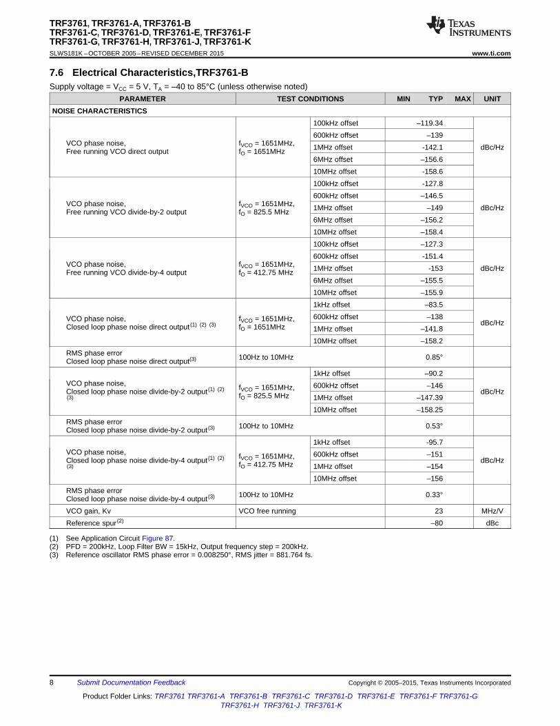
8.1 OverviewTRF3761 is an integrated frequency synthesizer with low-noise, voltage-controlled oscillator (VCO) and aninteger-N PLL. N-Divider block supports flexible output frequency range. A 3-wire serial-programming interface(SPI) interface is used to control the device. Device also supports power down feature through SPI interface orvia chip_en pin.
8.2 Functional Block Diagram
8.3 Feature Description
8.3.1 VCOThe TRF3761 integrates a high-performance, LC tank, voltage-controlled oscillator (VCO). For each of thedevices of the TRF3761 family, the inductance and capacitance of the tank are optimized to yield the best phase-noise performance. The VCO output is fed externally and to the prescaler through a series of very low noisebuffers, that greatly reduce the effect of load pulling onto the VCO.
Copyright © 2005–2015, Texas Instruments Incorporated Submit Documentation Feedback 35
Product Folder Links: TRF3761 TRF3761-A TRF3761-B TRF3761-C TRF3761-D TRF3761-E TRF3761-F TRF3761-GTRF3761-H TRF3761-J TRF3761-K

( )REF_IN
OUTDIV
PFD COUNTER num COUNTER
FF = F × N = × A + Prescalar × B
R
REF_INDIV
PFD
FR =
F
integer decimalnum
COUNTER integer COUNTER num decimal
N= x y ,
Prescalar
B = x and A = Prescalar × y
´ Þ
( )OUT
PFD
COUNTER COUNTER
FN = = A + Prescalar × Bnum
F
OUTF200MHz
Prescalarnum
£
TRF3761, TRF3761-A, TRF3761-BTRF3761-C, TRF3761-D, TRF3761-E, TRF3761-FTRF3761-G, TRF3761-H, TRF3761-J, TRF3761-KSLWS181K –OCTOBER 2005–REVISED DECEMBER 2015 www.ti.com
Feature Description (continued)8.3.2 Divide by 2, by 4, and Output BufferTo extend the frequency coverage, the TRF3761 integrates a divide by 2 and by 4 with a low noise floor. TheVCO signal is fed externally through a final open-collector differential-output buffer. This buffer is able to provideup to 3dBm (typical) of power into a 200Ω differential resistive load. The open-collector structure gives theflexibility to choose different load configurations to meet different requirements.
8.3.3 N-Divider
8.3.3.1 Prescaler StageThis stage divides down the VCO frequency before the A and B counters. This is a dual-modulus prescaler andthe user can select any of the following settings: 8/9, 16/17, 32/33, and 64/65. Prescaling is used due to the factthat the internal devices are limited in frequency operations of 200MHz. To determine the proper prescaler value,Fout which is the frequency out of the VCO is divided by the numerator of the prescaler if the answer is less than200 MHz then that is the prescalar to use, see Equation 1. If the value is higher than 200 MHz then repeat thisprocedure with the next prescalar numerator until a value of 200MHz or less is achieved. Refer to Synthesizing aSelected Frequency.
(1)
8.3.3.2 A and B Counter StageThe TRF3761 includes a 6-bit A counter and a 13-bit B counter that operate on the output of the prescaler. TheA counter can take values from 0 to 63, while the B counter can take values from 3 to 8191. Also, the value forthe B counter must be greater than or equal to the value for the A counter. The A and B counter with theprescaler stage create the VCO N-divider, see Equation 2 and Equation 3. Refer to Synthesizing a SelectedFrequency.
(2)
(3)
8.3.3.3 Reference DividerTRF3761 includes a 14-bit RDiv, also known as RDiv, that allows the input reference frequency to be divideddown to produce the reference clock to the phase frequency detector (PFD) this clock is also known as FPFDwhich is also the channel step size. Division ratios from 1 to 16,383 are allowed. To determine RDiv useEquation 4.
(4)
The output frequency (Fout) is determined using Equation 5.
(5)
8.3.4 Phase Frequency Detector (PFD) and Charge Pump StageThe outputs of the RDiv and the N counter are fed into the PFD stage, where the two signals are compared infrequency and phase. The TRF3761 features an anti-backlash pulse, whose width is controllable by the userthrough the serial programming interface. The PFD feeds the charge pump, whose output current pulses are fedinto an external loop filter, which eventually produces the tuning voltage needed to control the integrated VCO tothe desired frequency.
36 Submit Documentation Feedback Copyright © 2005–2015, Texas Instruments Incorporated
Product Folder Links: TRF3761 TRF3761-A TRF3761-B TRF3761-C TRF3761-D TRF3761-E TRF3761-F TRF3761-GTRF3761-H TRF3761-J TRF3761-K

TRF3761, TRF3761-A, TRF3761-BTRF3761-C, TRF3761-D, TRF3761-E, TRF3761-FTRF3761-G, TRF3761-H, TRF3761-J, TRF3761-K
www.ti.com SLWS181K –OCTOBER 2005–REVISED DECEMBER 2015
Feature Description (continued)8.3.5 Mux OutMUX_OUT pin (39) provides a communication port to the microcontroller circuit. See Table 4 in the DetailedDesign Procedure section.
8.3.6 Div 1/2/4Div 1/2/4 is the frequency divider for the TRF3761. This circuit can be programmed thru the serial programminginterface (SPI) to divide the output frequency of the VCO by 1, 2 or 4. This feature allows for the same loop filterdesign to be used for any of the 3 divide by modes, 1, 2 and 4. For example, if the VCO is running at 1499MHzto 1608MHz band then with the same exact circuit, run the output in the divide by 2 mode 749.5MHz to 804MHzband or in the divide by 4 mode 374.75MHz to 402MHz.
8.3.7 Serial interfaceThe programming interface pins (3, 4, 5) to the chip are the serial programming interface (SPI). The interfacerequires a Clock, Data, and Strobe signal to operate. See timing diagram Figure 83.
8.3.8 CHIP ENABLEThis feature provides a way to shut down the chip when not needed in order to conserve power. CHIP_EN Pin(2) needs to be High for normal operation.
8.3.9 Buffer Power DownPD_OUTBUFF pin (1), when enabled in software can provide a -40dB reduction in the output power while theVCO is locked and running. This feature is to help with isolation between RX and TX.
8.3.10 External VCO INEXT_VCO_IN pin (18) allows for the use of an external VCO to use the phase lock loop circuit in the TRF3761.This feature enables higher frequencies to be synthesized.
8.4 Device Functional Modes
8.4.1 Programmable Divider ModeTRF3761 frequency range is extended by integrating a divide by 2 and by 4 options. The VCO signal is fedexternally through differential-output buffer. The divider block allows to divide the output frequency of the VCO by1, 2 or 4 by programming thru serial programming interface (SPI). These 3 divide by modes of 1, 2 and 4enables the usage of same loop filter for wider frequency coverage.
Copyright © 2005–2015, Texas Instruments Incorporated Submit Documentation Feedback 37
Product Folder Links: TRF3761 TRF3761-A TRF3761-B TRF3761-C TRF3761-D TRF3761-E TRF3761-F TRF3761-GTRF3761-H TRF3761-J TRF3761-K

tsu1 th t(CLK)
tsu2 tw
1” Clock Pike
CLOCK
DATA
STROBE
DB0 (LSB)Address bit 1
DB1Address bit 2
DB2Address bit 3
DB29Cmd bit 30
DB30Cmd bit 31
DB31 (MSB)Cmd bit 32
TRF3761, TRF3761-A, TRF3761-BTRF3761-C, TRF3761-D, TRF3761-E, TRF3761-FTRF3761-G, TRF3761-H, TRF3761-J, TRF3761-KSLWS181K –OCTOBER 2005–REVISED DECEMBER 2015 www.ti.com
8.5 Programming
8.5.1 Serial Interface Programming Registers DefinitionThe TRF3761 features a 3-wire serial programming interface that controls an internal, 32-bit shift register. Thereare a total of 3 signals that need to be applied: the CLOCK (pin 3), the serial DATA (pin 4) and the STROBE (pin5). The DATA (DB0-DB31) is loaded LSB first and is read on the rising edge of the CLOCK. The STROBE isasynchronous to the CLOCK and at its rising edge the data in the shift register gets loaded onto the selectedinternal register. The first four bits (DB0-DB3) is the address to select the available internal registers.
A. The first 4 bits, DB(3-0), of data are Address bits. The 28 remaining bits, DB(31-4), are part of the command. Thecommand is little endian or lower bits first.
Figure 83. Serial Programming Timing Diagram
38 Submit Documentation Feedback Copyright © 2005–2015, Texas Instruments Incorporated
Product Folder Links: TRF3761 TRF3761-A TRF3761-B TRF3761-C TRF3761-D TRF3761-E TRF3761-F TRF3761-GTRF3761-H TRF3761-J TRF3761-K

TRF3761, TRF3761-A, TRF3761-BTRF3761-C, TRF3761-D, TRF3761-E, TRF3761-FTRF3761-G, TRF3761-H, TRF3761-J, TRF3761-K
www.ti.com SLWS181K –OCTOBER 2005–REVISED DECEMBER 2015
8.6 Register Maps
8.6.1 Register 1
Figure 84. Register 1: Device Setup
DB31 DB30 DB29 DB28 DB27 DB26 DB25 DB24 DB23 DB22 DB21 DB20 DB19 DB18 DB17 DB16Full CP_T TRIS_ PFD_ Anti Backlash Reference Clock Divider (RDiv)Cal EST CP POLReqR/W R/W R/W R/W R/W R/W
DB15 DB14 DB13 DB12 DB11 DB10 DB9 DB8 DB7 DB6 DB5 DB4 DB3 DB2 DB1 DB0Reference Clock Divider (RDiv) PD OUTB Output Mode Charge Pump Current Select Register Address
BUFO UF RESTUT EN_S
ELR/W R/W R/W R/W R/W R/W
LEGEND: R/W = Read/Write; R = Read only; -n = value after reset
Copyright © 2005–2015, Texas Instruments Incorporated Submit Documentation Feedback 39
Product Folder Links: TRF3761 TRF3761-A TRF3761-B TRF3761-C TRF3761-D TRF3761-E TRF3761-F TRF3761-GTRF3761-H TRF3761-J TRF3761-K

TRF3761, TRF3761-A, TRF3761-BTRF3761-C, TRF3761-D, TRF3761-E, TRF3761-FTRF3761-G, TRF3761-H, TRF3761-J, TRF3761-KSLWS181K –OCTOBER 2005–REVISED DECEMBER 2015 www.ti.com
Table 1. Register 1: Device SetupREGISTER 1 MAPPING
Data Field DB31 FULL_CAL_REQ This is a read only bit, that indicates if a 0 power-up cal is not requiredpower-up cal is required 1 power-up cal is required
DB30 CP_TEST TI internal use only 1 test enabled
DB29 TRIS_CP High-impedance state charge pump output 1 CP high-impedance state0 for normal operation
DB28 PFD_POL Selects Polarity of PFD, should match polarity 0 negativeof VCO gain. If using external VCO with 1 positiveNegative gain then set to 0 and vise versa.The internal VCO has positive gain so set topositve(1)
DB27 ABPW1 ABPW<1,0>: anti-backlash pulse width 00 1.5ns delay01 0.9ns delay10 3.8ns delay11 2.7ns delay
DB26 ABPW0
DB25 RDIV_13 14-bit reference clock divider RDIV<13,0>:00...01: divide by 1RDIV<13,0>:00...10: divide by 2DB24 RDIV_12 RDIV<13,0>:00...11: divide by 3
DB23 RDIV_11
DB22 RDIV_10
DB21 RDIV_9
DB20 RDIV_8
DB19 RDIV_7
DB18 RDIV_6
DB17 RDIV_5
DB16 RDIV_4
DB15 RDIV_3
DB14 RDIV_2
DB13 RDIV_1
DB12 RDIV_0
DB11 PD_BUFOUT If DB10 = 0 then it controls power down of <DB10:11>:output buffer 00 default; output buffer on
01 output buffer off1x output buffer on/off controlled byOUTBUF_EN pin
DB10 OUTBUF_EN_SEL Select Output Buffer enable control: 0 internal1 through OUTBUF_EN pin
DB9 OUT_MODE_1 OUTBUFMODE<1,0>: Selection of RF output 00 divide by 1buffer division ratio 01 divide by 2DB8 OUT_MODE_0 10 divide by4
DB7 ICP2 ICP<2,0>: select charge pump current (1 mAstep). From 1.4mA to 11.2mA with Rbias setDB6 ICP1 to 2.37Kohms.
DB5 ICP0
DB4 RESET Registers reset 1 high0 low for normal operation
Address Bits DB3 Address Bits <3,0>=0000 for register 1
DB2
DB1
DB0
40 Submit Documentation Feedback Copyright © 2005–2015, Texas Instruments Incorporated
Product Folder Links: TRF3761 TRF3761-A TRF3761-B TRF3761-C TRF3761-D TRF3761-E TRF3761-F TRF3761-GTRF3761-H TRF3761-J TRF3761-K

( )3.3252 × N + 1I =CP
Rbias1
1.2 V 22.168I = × (N + 1) ×CP
R 8bias1
TRF3761, TRF3761-A, TRF3761-BTRF3761-C, TRF3761-D, TRF3761-E, TRF3761-FTRF3761-G, TRF3761-H, TRF3761-J, TRF3761-K
www.ti.com SLWS181K –OCTOBER 2005–REVISED DECEMBER 2015
OUT_MODE<1,0>: TRF3761 has an optional divide by 2 or 4 output, which is selectable by programming bits<OUT_MODE_1, OUT_MODE_0> of register 1 (see Table 1).
CP_TEST: By setting bit DB30 to 1 it is possible to test the PFD up or down pulses. Internal TI use only.
TRIS_CP: If bit DB29 is set to 1, the charge pump output goes in tri-state. For normal operation, DB29 must beset to 0.
ABPW: Bits <DB27, DB26> are used to program the width of the anti-backlash pulses of the PFD. The userselects one of the following values: 0.9ns, 1.5ns, 2.7ns and 3.8ns. Backlash can occur when Fpfd becomesphase aligned with Fout of the VCO. This will cause a high impedance state on the phase detector and allow theoutput frequency to drift until the phase difference is enough to cause the phase detector to start sending signalsto the charge pump to correct the difference. This slight variation will show up as a sub harmonic of the pfdsignal in the passband of the loop filter which would result in a significant spur in the output of the VCO. It isrecommended that the anti-backlash pulse be set to the 1.5ns which gives the best spur reduction for theTRF3761.
PFD_POL: Bit DB28 of register 1 sets the polarity of the PFD. A Low (0) selects a negative polarity, and a High(1) selects a positive polarity. By choosing the correct polarity, the TRF3761 will works with an external VCOhaving both positive and negative gain (Kv). For example if an external VCO has a Kv = –23MHz/V then the PFDpolarity would need to be negative, so DB28 would be set to a Low (0). When using the internal VCO with a Kvof 23MHz/V, the PDF_POL should be set to 1.
RDiv: A 14-bit word programs the RDiv for the reference signal, DB25 is the MSB and DB12 is the LSB. RDivvalue is determined by dividing the reference frequency by the channel step size. For example if the referencefrequency is 10MHz and the channel step size is 200KHz then RDiv would be 50. This sets up the Fpfd for thephase detector, in other words the reference frequency will be divided down by a factor of RDiv which in thisexample is 50.
ICP: Bits <DB7, DB5> set the charge pump current.
(6)
which reduces to:
(7)
where N = decimal value of [Reg1 DB<7:5>]. The range is set by N and Rbias2. It is recommended that Icp beset to 7mA or <DB7, DB5>=101.
OUTBUF_EN_SEL: Output buffer on/off state is controlled through serial interface or an external pin. If bit DB10is a 0 (default state) the output buffers state is elected through bit DB11. If DB10 is a 1, the buffers on/off aredirectly controlled by the OUTBU_EN pin.
RESET: Setting bit DB4 to 1, all registers are reset to default values.
Refer to Register 1 under the Detailed Design Procedure section.
Copyright © 2005–2015, Texas Instruments Incorporated Submit Documentation Feedback 41
Product Folder Links: TRF3761 TRF3761-A TRF3761-B TRF3761-C TRF3761-D TRF3761-E TRF3761-F TRF3761-GTRF3761-H TRF3761-J TRF3761-K

TRF3761, TRF3761-A, TRF3761-BTRF3761-C, TRF3761-D, TRF3761-E, TRF3761-FTRF3761-G, TRF3761-H, TRF3761-J, TRF3761-KSLWS181K –OCTOBER 2005–REVISED DECEMBER 2015 www.ti.com
8.6.2 Register 2
Figure 85. Register 2: VCO Calibration
DB31 DB30 DB29 DB28 DB27 DB26 DB25 DB24 DB23 DB22 DB21 DB20 DB19 DB18 DB17 DB16STAR VCO Frequency in MHz ReferenceT_CAL Frequency
ContinuedR/W R/W R/W
DB15 DB14 DB13 DB12 DB11 DB10 DB9 DB8 DB7 DB6 DB5 DB4 DB3 DB2 DB1 DB0Reference Frequency (Fractional Part) Reference Frequency (Integer Part) Register Address
R/W R/W R/WLEGEND: R/W = Read/Write; R = Read only; -n = value after reset
Table 2. Register 2: VCO CalibrationREGISTER 2 MAPPINGData Field DB31 START_CAL 1 start calibration
DB30 FOUT12 VCO frequency in MHz start calibrationDB29 FOUT11DB28 FOUT10DB27 FOUT9DB26 FOUT8DB25 FOUT7DB24 FOUT6DB23 FOUT5DB22 FOUT4DB21 FOUT3DB20 FOUT2DB19 FOUT1DB18 FOUT0DB17 REF_FRAC6 Reference frequency in MHz (fractional 0000000 = 0.00MHz
part) 0000001 = 0.01MHzDB16 REF_FRAC5 0000010 = 0.02MHzDB15 REF_FRAC4 . . . . .
1100011 = 0.99MHzDB14 REF_FRAC3DB13 REF_FRAC2DB12 REF_FRAC1DB11 REF_FRAC0DB10 REF6 Reference frequency in MHz (integer 0001010 =10MHz
part) 0001011 =11MHzDB9 REF5 . . . . .DB8 REF4 1101000 = 104MHzDB7 REF3DB6 REF2DB5 REF1DB4 REF0
Address DB3 0 Address Bits <3,0>=0001 for register 2Bits DB2 0
DB1 0DB0 1
42 Submit Documentation Feedback Copyright © 2005–2015, Texas Instruments Incorporated
Product Folder Links: TRF3761 TRF3761-A TRF3761-B TRF3761-C TRF3761-D TRF3761-E TRF3761-F TRF3761-GTRF3761-H TRF3761-J TRF3761-K

TRF3761, TRF3761-A, TRF3761-BTRF3761-C, TRF3761-D, TRF3761-E, TRF3761-FTRF3761-G, TRF3761-H, TRF3761-J, TRF3761-K
www.ti.com SLWS181K –OCTOBER 2005–REVISED DECEMBER 2015
Reference Frequency: The 14 bits <DB17, DB4> are used to specify the input reference frequency as multiplesof 10kHz. Bits <DB10,DB4> specify the integer part of the reference frequency expressed in MHz. Bits<DB17,DB11> set the fraction part. Those values are then used during the calibration of the internal VCO. Forexample if using a 20MHz reference oscillator then bits<DB10,DB4> would be 0010100 and bits<DB17,DB11>would be 0000000. If the reference oscillator is 13.1MHz then bits<DB10,DB4> would be 0001101 andbits<DB17,DB11> would be 0001010.
Start Calibration: A 1 in DB31 starts the internal VCO calibration. When the calibration is complete, DB31 bit isinternally reset to 0.
FOUT<12,0>: This 13-bit word <DB30,DB18> specifies the VCO output frequency in MHz. If output frequency isnot a integer multiple of MHz, this value must be approximated to the closest integer in MHz.
Refer to Register 2 under the Detailed Design Procedure section.
Copyright © 2005–2015, Texas Instruments Incorporated Submit Documentation Feedback 43
Product Folder Links: TRF3761 TRF3761-A TRF3761-B TRF3761-C TRF3761-D TRF3761-E TRF3761-F TRF3761-GTRF3761-H TRF3761-J TRF3761-K

TRF3761, TRF3761-A, TRF3761-BTRF3761-C, TRF3761-D, TRF3761-E, TRF3761-FTRF3761-G, TRF3761-H, TRF3761-J, TRF3761-KSLWS181K –OCTOBER 2005–REVISED DECEMBER 2015 www.ti.com
8.6.3 Register 3
Figure 86. Register 3: A and B Counters
DB31 DB30 DB29 DB28 DB27 DB26 DB25 DB24 DB23 DB22 DB21 DB20 DB19 DB18 DB17 DB16RSRV RSRV Lock Test MUX B-Counter
PLLR/W R/W R/W R/W R/W
DB15 DB14 DB13 DB12 DB11 DB10 DB9 DB8 DB7 DB6 DB5 DB4 DB3 DB2 DB1 DB0B-Counter A-Counter Dual-Modulus Register Address
Prescalar ModeR/W R/W R/W R/W
LEGEND: R/W = Read/Write; R = Read only; -n = value after reset
Table 3. Register 3: A and B CountersREGISTER 3 MAPPINGData Field DB31 Rsrv Reserved
DB30 Rsrv ReservedDB29 START_LK Lock PLL to frequency 1 activeDB28 TEST_MUX_3 See Table 4 for descriptions and 0001 = LOCK_DETECT enabled
settings.DB27 TEST_MUX_2DB26 TEST_MUX_1DB25 TEST_MUX_0DB24 B_12 13-bit B counterDB23 B_11DB22 B_10DB21 B_9DB20 B_8DB19 B_7DB18 B_6DB17 B_5DB16 B_4DB15 B_3DB14 B_2DB13 B_1DB12 B_0DB11 A_5 6-bit A counterDB10 A_4DB9 A_3DB8 A_2DB7 A_1DB6 A_0DB5 PRESC_MOD1 Dual-modulus prescaler mode <B5,B4>:00 for 8/9
<B5,B4>:01 for 16/17DB4 PRESC_MOD0 <B5,B4>:10 for 32/33<B5,B4>:11 for 64/65
Address DB3 0 Address Bits <3,0>=0010 for register 3Bits DB2 0
DB1 1DB0 0
44 Submit Documentation Feedback Copyright © 2005–2015, Texas Instruments Incorporated
Product Folder Links: TRF3761 TRF3761-A TRF3761-B TRF3761-C TRF3761-D TRF3761-E TRF3761-F TRF3761-GTRF3761-H TRF3761-J TRF3761-K

TRF3761, TRF3761-A, TRF3761-BTRF3761-C, TRF3761-D, TRF3761-E, TRF3761-FTRF3761-G, TRF3761-H, TRF3761-J, TRF3761-K
www.ti.com SLWS181K –OCTOBER 2005–REVISED DECEMBER 2015
B<12,0>: This 13-bit word <DB24,DB12> controls the value of the B counter of the N divider. The valid range isfrom 3 to 8191.
A<5,0>: These 6 bits <DB11,DB6> control the value of the A counter. The valid range is from 0 to 63.
PRESC_MOD<1,0>: These bits <DB5,DB4> define the mode of the dual-modulus prescaler according toTable 3.
START_LK: TRF3761 does not load the serial interface registers values into the dividers registers until bit DB29of register 3 is set to 1. After TRF3761 is locked to the new frequency, bit DB29 is internally reset to 0.
Refer to Register 3 under the Detailed Design Procedure section.
Copyright © 2005–2015, Texas Instruments Incorporated Submit Documentation Feedback 45
Product Folder Links: TRF3761 TRF3761-A TRF3761-B TRF3761-C TRF3761-D TRF3761-E TRF3761-F TRF3761-GTRF3761-H TRF3761-J TRF3761-K

= 2πFc cv
OUTFN =
Fcom
OUTF = F Fmin max
TRF3761, TRF3761-A, TRF3761-BTRF3761-C, TRF3761-D, TRF3761-E, TRF3761-FTRF3761-G, TRF3761-H, TRF3761-J, TRF3761-KSLWS181K –OCTOBER 2005–REVISED DECEMBER 2015 www.ti.com
9 Application and Implementation
NOTEInformation in the following applications sections is not part of the TI componentspecification, and TI does not warrant its accuracy or completeness. TI’s customers areresponsible for determining suitability of components for their purposes. Customers shouldvalidate and test their design implementation to confirm system functionality.
9.1 Application InformationThe TRF3761 device is suited for high performance RF transmit signal chain applications such as wireless radiotransmitters.
9.1.1 Loop Filter DesignNumerous methodologies and design techniques exist for designing optimized loop filters for particularapplications. The loop filter design can affect the stability of the loop, the lock time, the bandwidth, the extraattenuation on the reference spurs, etc. The role of the loop filter is to integrate and lowpass the pulses of thecharge pump and eventually yield an output tuning voltage that drives the VCO. Several filter topologies can beimplemented, including both passive and active. In this section, a third-order passive filter is used. For thisexample, assume these several design parameters. The internal VCO has a value of 23MHz/V, meaning that inthe linear region, changing the tuning voltage of the VCO by 1V induces a change of the output frequency ofabout 23MHz. It is known that N = 4500 and Fpfd = 200kHz from our previous example. It is assumed thatcurrent setting in register 1 <DB7:DB5> is set to 100 and sets a maximum current of 5.6mA.TI recommends anIcp of 5.6mA, which give the best spur performance, but can be changed for different application. In addition, thebandwidth of the loop filter must be determined. This is a critical consideration as it affects the lock time of thesystem. Assuming an approximate bandwidth of around 20kHz is required and that for stability a phase margin ofabout 45 degrees is desired, the following values for the components of the loop filter can be derived. There isalmost an infinite number of solutions to the problem of designing the loop filter and the designer is called tomake tradeoff decisions for each application. Texas Instruments has provided a loopfilter program in the productfolder for the TRF3761.
Some terms are interchangeable and are described and equated here:• Fcom = FPDF which identify the comparing frequency or phase detector frequency which is also equal to the
system channel step size. FOUT must be a multiple of Fcom.• Fmin is the lower frequency of the design band.• Fmax is the upper frequency of the design band.• Fref is the reference frequency for the PLL. Fref must be a multiple of Fcom.• Kvco = Kv expressed in MHz per Volt (MHz/V) which is the gain of the VCO. The TRF3761 internal VCO has a
Kv = 23MHz/V.• Icp is the charge pump current. The TRF3761 is typically set to 5.6mA.• Fc is the loop filter bandwidth which should be no more than 1/10 Fcom.• φ is phase margin in degrees. Values should be between 30 and 70. The higher the phase margin the better
the stability of the PLL but the slower the lock time. 45 degrees is a good tradeoff.• T3/T1 in percent is the percentage of the poles in the loop filter. Usually set to 45%. The higher the value
(closer to 100%) the more the spurs are attenuated, but peaking occurs in the pass band of the loop filter.
(8)
(9)
(10)
46 Submit Documentation Feedback Copyright © 2005–2015, Texas Instruments Incorporated
Product Folder Links: TRF3761 TRF3761-A TRF3761-B TRF3761-C TRF3761-D TRF3761-E TRF3761-F TRF3761-GTRF3761-H TRF3761-J TRF3761-K

T2 T3R1 = , R2 =
C2 C3
T2 C1C2 = C1 - 1 , C3 =
T1 10
æ öç ÷è ø
( )
( )( )VCO
1
22
1 + T2K KT1 cC1 = × x
2T2 2 2 2 2N 1 + T1 1 + T3c c c
é ùê úvf ê úê úv v vê úë û
( )
1T2 =
2T1+T3cv
T3T3 = T1
T1
æ öç ÷è ø
1- tan
cosT1
T31 +c
T1
æ öfç ÷fè ø=
æ öv ç ÷
è ø
TRF3761, TRF3761-A, TRF3761-BTRF3761-C, TRF3761-D, TRF3761-E, TRF3761-FTRF3761-G, TRF3761-H, TRF3761-J, TRF3761-K
www.ti.com SLWS181K –OCTOBER 2005–REVISED DECEMBER 2015
Application Information (continued)
(11)
(12)
(13)
(14)
(15)
(16)
Copyright © 2005–2015, Texas Instruments Incorporated Submit Documentation Feedback 47
Product Folder Links: TRF3761 TRF3761-A TRF3761-B TRF3761-C TRF3761-D TRF3761-E TRF3761-F TRF3761-GTRF3761-H TRF3761-J TRF3761-K

TRF3761
(TOP VIEW)
GND
AVDD_BIAS
RBIAS1
GND
VCTRL_IN
AVDD_VCO
AVDD_BUF
AVDD_CAPARRAY
GND
AVDD
(See Note A)
PD_OUTBUF
CHIP_EN
CLOCK
DATA
STROBE
DGND
DGND
DVDD1
AVDD_PRES
GND
DV
DD
2
MU
X_O
UT
RE
F_IN
GN
D
AV
DD
_R
EF
AV
DD
_C
P
CP
OU
T
GN
D
AV
DD
GN
D
GN
D
GN
D
VC
O_O
UT
P
VC
O_O
UT
M
AV
DD
_O
UT
BU
F
GN
D
AV
DD
_V
CO
BU
F
EX
T_V
CO
_IN
RB
IAS
2
GN
D
1
2
3
4
5
6
7
8
9
10
30
29
28
27
26
25
24
23
22
21
383940 37 36 35 34 33 32 31
131211 14 15 16 17 18 19 20
To
Mic
roco
ntr
olle
r
To
Mic
roco
ntr
olle
r
RE
F
C41000 pF
R32.37 kΩ
C1R1
C2
C3
R2
C610 pF
C510 pF
R5120 Ω
R6120 Ω
VDDVDD
LOAD
C71000 pF
R44.75 kΩ
TRF3761, TRF3761-A, TRF3761-BTRF3761-C, TRF3761-D, TRF3761-E, TRF3761-FTRF3761-G, TRF3761-H, TRF3761-J, TRF3761-KSLWS181K –OCTOBER 2005–REVISED DECEMBER 2015 www.ti.com
9.2 Typical ApplicationsFigure 87 shows a typical application schematic for the TRF3761. In this example, the output signal is takendifferential using the 2 resistive pull-up resistors of the final output buffer. A single-ended and tuned loadconfiguration is also available.
The loop filter components:C1 = 303pF, R1 = 8.87kΩ, C2 = 1650pF, R2 = 3.4kΩ, C3 = 330pF
are the typical values used for the Figure 87. The values can be optimized differently according to therequirements of the different applications.
A. Refer to the Loop Filter Design section.
Figure 87. TRF3761 Application Schematic
9.2.1 Design Requirements
9.2.1.1 Loop Filter Design ExampleGiven these parameters which were used for the lock time plot in Figure 88:• Fmin = 2085 MHz• Fmax = 2175 MHz• Fcom = 400 KHz• Icp = 4.2mA• Kvco = 23 MHz• Fc = 20 KHz• Phase Margin = 45 degrees• T3/T1 = 45%
48 Submit Documentation Feedback Copyright © 2005–2015, Texas Instruments Incorporated
Product Folder Links: TRF3761 TRF3761-A TRF3761-B TRF3761-C TRF3761-D TRF3761-E TRF3761-F TRF3761-GTRF3761-H TRF3761-J TRF3761-K

T3R3 = = 30.2kΩ
C3
T2R2 = = 7.61kΩ
C2
C1C3 = = 33.87pF
10
T2C2 = C1 - 1 = 2524.14pFT1
æ öç ÷è ø
( )
( )( )2
2 2 2 2 2
VCO
1
21 + TK KT c 21C1 = × × = 338.75pF
T2 N 1 + T 1 + Tc c c1 3
é ùê úvf ê úê úv v vê úë û
( )
1 -6T = = 19.2 x 10²
2T + T1 3C
v
T -63T = T = 1 x 10³ 1T1
æ öç ÷è ø
1- tan
cos -6T = = 2.3 x 101
T31 +c T1
æ öfç ÷fè ø
æ öv ç ÷è ø
3= 2πF = 125.66 x 10c cv
OUTFN = = 5325
Fcom
OUTF = F F = 2130MHz (rounded up)min max
TRF3761, TRF3761-A, TRF3761-BTRF3761-C, TRF3761-D, TRF3761-E, TRF3761-FTRF3761-G, TRF3761-H, TRF3761-J, TRF3761-K
www.ti.com SLWS181K –OCTOBER 2005–REVISED DECEMBER 2015
Typical Applications (continued)Calculate FOUT of design
(17)
Next calculate N
(18)
Then calculate ωc
(19)
Now calculate T1-T3 to give the RC time constants.
(20)
Use T1 to find T3
(21)
Then use T1 and T3 to find T2
(22)
Now C1, C2, C3, R1, and R2 are calculated using T1, T2, and T3.
(23)
(24)
(25)
Now using C2 and T2, find R2. Use C3 and T3 to find R3
(26)
(27)
R2 x C3 can be scaled using T3, so if C3 = 330pF, then R2 = 3.03 kΩ => 3.4 kΩ in the loop filter. R1 × C2 canbe scaled using T2. Scaling these values helps to improve the lock time. The actual values used in the lock timeplot were optimized for lock time as well as using real valued components. The values in figure 62 were takenfrom the current EVM schematic.
Copyright © 2005–2015, Texas Instruments Incorporated Submit Documentation Feedback 49
Product Folder Links: TRF3761 TRF3761-A TRF3761-B TRF3761-C TRF3761-D TRF3761-E TRF3761-F TRF3761-GTRF3761-H TRF3761-J TRF3761-K

TRF3761, TRF3761-A, TRF3761-BTRF3761-C, TRF3761-D, TRF3761-E, TRF3761-FTRF3761-G, TRF3761-H, TRF3761-J, TRF3761-KSLWS181K –OCTOBER 2005–REVISED DECEMBER 2015 www.ti.com
Typical Applications (continued)9.2.2 Detailed Design Procedure
9.2.2.1 Initial Calibration and Frequency Setup at Power UpThe integrated high performance VCO requires an internal frequency calibration at power up. To perform suchcalibration the following procedure is recommended:• Apply 5V power supply to IC.• Apply an input reference frequency to pin (38) and ensure the signal is stable.• Turn on the TRF3761 using the chip enable pin (CHIP_EN, pin 2), by applying 5V.
9.2.2.1.1 Register 1• Setup the device through Register 1 referencing Table 1.
a. The first 4 bits of the 32-bit code sent to the chip are set DB <3:0> to 0000; which is the address ofregister 1.
b. Bit 5, DB4, sets the soft reset for the chip. Soft reset allows for the registers to be reset without poweringdown the chip. If a soft reset is used then write to register 1 twice: once with DB4 set high and once withDB4 set low. Typically, this bit is only used when the chip has been powered up and registers 1, 2, and 3have already been written to, so on power-up reset is not required, so DB4 is, by default, set low.
c. DB <7: 5> sets the charge pump current based on the resistor value on pin 28 of the TRF3761 and thedecimal value of Register 1, DB<7:5> used in Equation 6. This equation reduces to Equation 7, whereN = decimal value of [Reg1 DB<7:5>].
d. DB <9: 8> sets the mode of the chip. The mode is how the device will or will not divide down the VCO’sfrequency. There are 3 choices for the mode setting, divide by 1, 2 or 4 per Table 1. For example, if393.75MHz is required from the TRF3761 which has a main frequency of 1575MHz then the divide-by-4mode is chosen by setting DB <9: 8> to 10.
e. DB <11:10> controls the output buffer. Both of these are set to 00 by default, so the buffer is controlledinternally. Refer to Table 1 for more information.
f. DB <25:12> sets the RDiv value. Once the calculations under the Synthesizing a Selected Frequencysection have been completed the value is known, based on the external reference oscillator. The valuefor R is entered into the DB <25:12>. For example, if the reference oscillator is at a frequency (FREF_IN) of61.44MHz and a channel step size of 120kHz is required, which is also the frequency (FPFD) the phasefrequency detector will use to compare against the VCO's output frequency (FOUT), then FREF_IN /FPFD =512, which is entered as follows: MSB: LSB 0001000000000.
g. By default, DB <27:26> are set to 00 for a 1.5ns delay on the anti-backlash pulse width. Refer to Table 1for more information.
h. DB 28 is set to 1 for positive by default. Refer to Table 1 for more information.i. DB 29 is set to 0 for normal operation. Refer to Table 1 for more information.j. DB 30 is set to 0 by default. Refer to Table 1 for more information.k. DB 31 is set to 0 by default. Refer to Table 1 for more information.
50 Submit Documentation Feedback Copyright © 2005–2015, Texas Instruments Incorporated
Product Folder Links: TRF3761 TRF3761-A TRF3761-B TRF3761-C TRF3761-D TRF3761-E TRF3761-F TRF3761-GTRF3761-H TRF3761-J TRF3761-K

TRF3761, TRF3761-A, TRF3761-BTRF3761-C, TRF3761-D, TRF3761-E, TRF3761-FTRF3761-G, TRF3761-H, TRF3761-J, TRF3761-K
www.ti.com SLWS181K –OCTOBER 2005–REVISED DECEMBER 2015
Typical Applications (continued)9.2.2.1.2 Register 2• Initiate calibration procedure by programming register 2 as follows: Reference Table 2.
a. The first 4 bits of the 32-bit code sent to the chip are set DB <3:0> to 0001; which is the address ofregister 2.
b. Use bits DB<17, 4> of register 2 to specify the input reference frequency in MHz. The value is split intoan integer and a fraction part. For example: to insert a fREF of 30.72MHz, set:– DB<10, 4> (integer part) equal to 0011110 (30) and– DB<17, 11> (fraction part) equal to 1001000 (72).
c. Set DB<30:18> of register 2 to the desired frequency. For example: 2200MHz would be 0100010011000(2200).
d. Set DB31of register 2 to 1 to start the calibration. The VCO calibration runs for 5ms. During the calprocedure it will not be possible to program register 2 and 3. At the end of the calibration, bit DB31 ofregister 2 resets to 0.
e. Subsequent frequency programming requires DB31 to be set to 0.
9.2.2.1.3 Register 3• Completion of the frequency set up, on initial calibration, cannot proceed until 5ms has elapsed, due to full
calibration, then it will require that the A and B values, the prescalar ratio, be known. Refer to Synthesizing aSelected Frequency section for calculation. Reference Table 3.a. The first 4 bits of the 32-bit code sent to the chip are set DB <3:0> to 0010; which is the address of
register 3.b. DB<5:4> sets the prescalar ratio, 8/9, 16/17, 32/33, 64/65. For example: if 16/17 are required, set the
register bits DB<5:4> to 01.c. DB<11:6> sets the A value for the N counter. For example: if A is 4, set DB<11:6> as follows: 000100 (4).d. DB<24:12> sets the B value for the N counter. For example: if B is 1156, set DB<24:12> as follows:
0010010000100 (4).e. DB<28:25> sets the TEST_MUX. This allows the user to check via the microcontroller the state of the
TRF3761 by programming it to one of 6 states. The most common state to use is the Digital lock Detectwhich places the pin in a logic high state with indicates the VCO is locked.
Table 4. MUX-Out SettingsSTATE DB<28:25> STATE DB<28:25>3-state o/p ( High impedance state on Pin 39) 0000 RDiv o/p (Shows R-value on Pin 39) 0100Digital lock Detect (High when locked on Pin 39) 0001 Analog lock detect (High when locked on Pin 39) 0101N-Divider o/p (Shows N-value on Pin 39) 0010 Read back ( read back register settings) 0110DVDD (internal TI use) 0011 DGND (internal TI use) 0111
f. DB29 sets the START LOCK, which is set to 0, on the initial frequency setup and then set to 1 onadditional frequency changes.
Once all registers are written, the TRF3761 will lock to the desired frequency. In order to change the frequencyonce the initial calibration is complete, only registers 2 and 3 need to be reprogrammed. No calibration isrequired.
Copyright © 2005–2015, Texas Instruments Incorporated Submit Documentation Feedback 51
Product Folder Links: TRF3761 TRF3761-A TRF3761-B TRF3761-C TRF3761-D TRF3761-E TRF3761-F TRF3761-GTRF3761-H TRF3761-J TRF3761-K

Loop filter Component:C1 = 303pF
R1 = 8.87k
R2 = 3.4kC2 = 1650pFC3 = 330pF
W
W
Frequency jump from1046MHz to 1085MHz:
Locktime freq ~ 250 sm
+5.000k
+4.000k
+3.000k
+2.000k
+1.000k
1.085G
-1.000k
-2.000k
-3.000k
-4.000k
-5.000k
TRF3761, TRF3761-A, TRF3761-BTRF3761-C, TRF3761-D, TRF3761-E, TRF3761-FTRF3761-G, TRF3761-H, TRF3761-J, TRF3761-KSLWS181K –OCTOBER 2005–REVISED DECEMBER 2015 www.ti.com
9.2.2.2 Re-Calibration After Power UpAssuming the TRF3761 is powered up and operational, a VCO calibration is also possible without poweringdown the IC. To perform such calibration the following procedure is recommended:• Set bit DB4 (RESET) of register 1 to 1. This performs a software reset and clears all registers of VCO
calibration data. Once the reset command is issued then DB4 of register 1 will need to be set to 0.• Repeat the Initial Calibration and Frequency Setup at Power Up section, skipping the power up section and
performing the register programming sequence.
9.2.2.3 Synthesizing a Selected FrequencyThe TRF3761 is an integer-N PLL synthesizer, and because of its flexibility (14-bit RDiv, 6-bit A counter, 13-bit Bcounter, and dual modulus prescaler), is ideal for synthesizing virtually any desired frequency. If synthesizing a900MHz local oscillator, with spacing capability (minimum frequency increment) of 200kHz, as in a typical GSMapplication, the choice of the external reference oscillator is beyond the scope of this section. However, if a10MHz reference is selected, the settings are calculated to yield the desired output frequency and channelspacing. There is more than one solution to a specific set of conditions, so below is one way of achieving thedesired result. First, select the appropriate RDiv counter value. Since a channel spacing of 200kHz is desired,the FPFD is set to 200kHz. Calculate the RDiv value through:
RDiv = FREFIN/FPFD = 10MHz/ 200kHz = 50 (28)
Assume a prescaler value of 8/9 is selected. This is a valid choice, since the prescaler output is well within the200MHz limit (900MHz / 8 = 112.5MHz). Select the appropriate A and B counter values.
RFOUT = FPFD × N = (FREFIN / RDiv) × (A counter + Prescalar numerator × B counter). (29)
Therefore, Equation 30 must be solved:900MHz = 200kHz x (A + 8 × B). (30)
There are many solutions to this single equation with two unknowns; there are some basic constraints on thesolution, since 3 ≤ B ≤ 8191, and also B ≥ A. So, if A = 4, solving the equation yields B = 562. One completesolution would be to choose:
RDiv = 50, A counter = 4, Bcounter = 562 and Prescalar = 8/9
resulting in the desired N counter value = 4500. This is how the A counter, B counter and prescalar make up theN counter.
When this procedure is complete the values for the N counter , R, and the prescalar ratio should be known.Registers 2 and 3 need to be set up for operation of the chip. Refer to Table 2 and Table 3 for this procedure.Register 2 bits <DB30:DB18> 12:0 set the output frequency of the device along with register 3. Refer to N-Divider section under the Feature Description.
9.2.3 Application Curve
Figure 88. Frequency Locktime52 Submit Documentation Feedback Copyright © 2005–2015, Texas Instruments Incorporated
Product Folder Links: TRF3761 TRF3761-A TRF3761-B TRF3761-C TRF3761-D TRF3761-E TRF3761-F TRF3761-GTRF3761-H TRF3761-J TRF3761-K
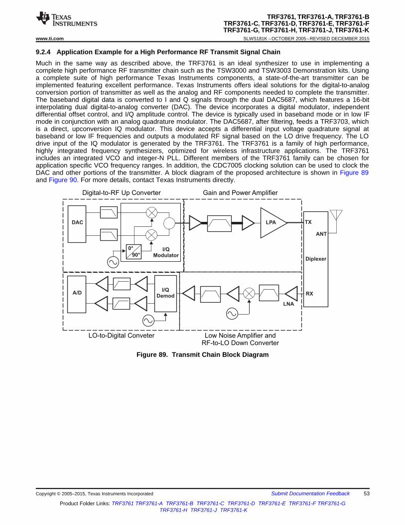
90°
0°
LPA TX
ANT
Diplexer
RX
DAC
A/DI/Q
Demod
I/QModulator
LNA
Low Noise Amplifier andRF-to-LO Down Converter
LO-to-Digital Conveter
Gain and Power AmplifierDigital-to-RF Up Converter
TRF3761, TRF3761-A, TRF3761-BTRF3761-C, TRF3761-D, TRF3761-E, TRF3761-FTRF3761-G, TRF3761-H, TRF3761-J, TRF3761-K
www.ti.com SLWS181K –OCTOBER 2005–REVISED DECEMBER 2015
9.2.4 Application Example for a High Performance RF Transmit Signal ChainMuch in the same way as described above, the TRF3761 is an ideal synthesizer to use in implementing acomplete high performance RF transmitter chain such as the TSW3000 and TSW3003 Demonstration kits. Usinga complete suite of high performance Texas Instruments components, a state-of-the-art transmitter can beimplemented featuring excellent performance. Texas Instruments offers ideal solutions for the digital-to-analogconversion portion of transmitter as well as the analog and RF components needed to complete the transmitter.The baseband digital data is converted to I and Q signals through the dual DAC5687, which features a 16-bitinterpolating dual digital-to-analog converter (DAC). The device incorporates a digital modulator, independentdifferential offset control, and I/Q amplitude control. The device is typically used in baseband mode or in low IFmode in conjunction with an analog quadrature modulator. The DAC5687, after filtering, feeds a TRF3703, whichis a direct, upconversion IQ modulator. This device accepts a differential input voltage quadrature signal atbaseband or low IF frequencies and outputs a modulated RF signal based on the LO drive frequency. The LOdrive input of the IQ modulator is generated by the TRF3761. The TRF3761 is a family of high performance,highly integrated frequency synthesizers, optimized for wireless infrastructure applications. The TRF3761includes an integrated VCO and integer-N PLL. Different members of the TRF3761 family can be chosen forapplication specific VCO frequency ranges. In addition, the CDC7005 clocking solution can be used to clock theDAC and other portions of the transmitter. A block diagram of the proposed architecture is shown in Figure 89and Figure 90. For more details, contact Texas Instruments directly.
Figure 89. Transmit Chain Block Diagram
Copyright © 2005–2015, Texas Instruments Incorporated Submit Documentation Feedback 53
Product Folder Links: TRF3761 TRF3761-A TRF3761-B TRF3761-C TRF3761-D TRF3761-E TRF3761-F TRF3761-GTRF3761-H TRF3761-J TRF3761-K

DAC5687
CLK1 CLK2
CDCM7005
Clock GeneratorVCXO
Ref Osc
TRF3761
PLL
LO Generator
TRF3703
I/Q
Modulator
16
16
RF Out
TRF3761, TRF3761-A, TRF3761-BTRF3761-C, TRF3761-D, TRF3761-E, TRF3761-FTRF3761-G, TRF3761-H, TRF3761-J, TRF3761-KSLWS181K –OCTOBER 2005–REVISED DECEMBER 2015 www.ti.com
Figure 90. Transmit Chain Block Diagram
10 Power Supply RecommendationsTRF3761 should be supplied with a low noise 4.5-V to 5.25-V supply as required. Each supply pin shouldgenerally be isolated from the main power bus with a ferrite or other noise filtering component.
54 Submit Documentation Feedback Copyright © 2005–2015, Texas Instruments Incorporated
Product Folder Links: TRF3761 TRF3761-A TRF3761-B TRF3761-C TRF3761-D TRF3761-E TRF3761-F TRF3761-GTRF3761-H TRF3761-J TRF3761-K

BOTTOM
GND
BOTTOM
GND
De-coupling
Capacitor’s
on back side
of board
De-coupling
Capacitor’s
on top side
of board
TOP
GND
Via to bottom ground
MU
X_
OU
T
BOTTOM
GND
BOTTOM
GND
De-coupling
Capacitor’s
on back side
of board
De-coupling
Capacitor’s
on top side
of board
TOP
GND
Via to bottom ground
BOTTOM
GND
BOTTOM
GND
De-coupling
Capacitor’s
on back side
of board
De-coupling
Capacitor’s
on top side
of board
TOP
GND
Via to bottom ground
BOTTOM
GND
BOTTOM
GND
De-coupling
Capacitor’s
on back side
of board
De-coupling
Capacitor’s
on top side
of board
TOP
GND
Via to bottom ground
MU
X_
OU
T
TRF3761, TRF3761-A, TRF3761-BTRF3761-C, TRF3761-D, TRF3761-E, TRF3761-FTRF3761-G, TRF3761-H, TRF3761-J, TRF3761-K
www.ti.com SLWS181K –OCTOBER 2005–REVISED DECEMBER 2015
11 Layout
11.1 Layout GuidelinesWhen designing the complete PLL, this section is of paramount importance in achieving the desiredperformance. Wherever possible, a multi-layer PCB board should be used, with at least one dedicated groundplane. A dedicated power plane (split between the supplies if necessary) is also recommended. The impedanceof all RF traces (the VCO output and feedback into the PLL) should be controlled to 50Ω. All small value (10pFand 0.1µF) decoupling capacitors should be placed as close to the device pins as possible. It is alsorecommended that both top and bottom layers of the circuit board be flooded with ground, with plenty of groundvias dispersed as appropriate. Because the digital lines are not in use during normal operation of the device andare only used to program the device on start up and during frequency changes the analog grounds (GND) anddigital grounds (DGND) are tied to the same ground plane. The most sensitive part of any PLL is the sectionbetween the charge pump output and the input to the VCO. This includes the loop filter components, and thecorresponding traces. The charge pump is a precision element of the PLL and any extra leakage on its path canadversely affect performance. Extra care should be given to ensure that parasitics are minimized in the chargepump output, and that the trace runs are short and optimized. Similarly, it is also recommend that extra care istaken in ensuring that any flux residue is thoroughly cleaned and moisture baked out of the PCB. From an EMIperspective, and since the synthesizer is typically a small portion of a bigger, complex circuit board, shielding isrecommended to minimize EMI effects.
11.2 Layout Example
A. Refer to the Loop Filter Design section.
Figure 91. TRF3761 Layout
Copyright © 2005–2015, Texas Instruments Incorporated Submit Documentation Feedback 55
Product Folder Links: TRF3761 TRF3761-A TRF3761-B TRF3761-C TRF3761-D TRF3761-E TRF3761-F TRF3761-GTRF3761-H TRF3761-J TRF3761-K

TRF3761, TRF3761-A, TRF3761-BTRF3761-C, TRF3761-D, TRF3761-E, TRF3761-FTRF3761-G, TRF3761-H, TRF3761-J, TRF3761-KSLWS181K –OCTOBER 2005–REVISED DECEMBER 2015 www.ti.com
12 Device and Documentation Support
12.1 Related LinksThe table below lists quick access links. Categories include technical documents, support and communityresources, tools and software, and quick access to sample or buy.
Table 5. Related LinksTECHNICAL TOOLS & SUPPORT &PARTS PRODUCT FOLDER SAMPLE & BUY DOCUMENTS SOFTWARE COMMUNITY
TRF3761 Click here Click here Click here Click here Click hereTRF3761-A Click here Click here Click here Click here Click hereTRF3761-B Click here Click here Click here Click here Click hereTRF3761-C Click here Click here Click here Click here Click hereTRF3761-D Click here Click here Click here Click here Click hereTRF3761-E Click here Click here Click here Click here Click hereTRF3761-F Click here Click here Click here Click here Click hereTRF3761-G Click here Click here Click here Click here Click hereTRF3761-H Click here Click here Click here Click here Click hereTRF3761-J Click here Click here Click here Click here Click hereTRF3761-K Click here Click here Click here Click here Click here
12.2 Community ResourcesThe following links connect to TI community resources. Linked contents are provided "AS IS" by the respectivecontributors. They do not constitute TI specifications and do not necessarily reflect TI's views; see TI's Terms ofUse.
TI E2E™ Online Community TI's Engineer-to-Engineer (E2E) Community. Created to foster collaborationamong engineers. At e2e.ti.com, you can ask questions, share knowledge, explore ideas and helpsolve problems with fellow engineers.
Design Support TI's Design Support Quickly find helpful E2E forums along with design support tools andcontact information for technical support.
12.3 TrademarksE2E is a trademark of Texas Instruments.All other trademarks are the property of their respective owners.
12.4 Electrostatic Discharge CautionThese devices have limited built-in ESD protection. The leads should be shorted together or the device placed in conductive foamduring storage or handling to prevent electrostatic damage to the MOS gates.
12.5 GlossarySLYZ022 — TI Glossary.
This glossary lists and explains terms, acronyms, and definitions.
13 Mechanical, Packaging, and Orderable InformationThe following pages include mechanical, packaging, and orderable information. This information is the mostcurrent data available for the designated devices. This data is subject to change without notice and revision ofthis document. For browser-based versions of this data sheet, refer to the left-hand navigation.
56 Submit Documentation Feedback Copyright © 2005–2015, Texas Instruments Incorporated
Product Folder Links: TRF3761 TRF3761-A TRF3761-B TRF3761-C TRF3761-D TRF3761-E TRF3761-F TRF3761-GTRF3761-H TRF3761-J TRF3761-K

PACKAGE OPTION ADDENDUM
www.ti.com 10-Dec-2020
Addendum-Page 1
PACKAGING INFORMATION
Orderable Device Status(1)
Package Type PackageDrawing
Pins PackageQty
Eco Plan(2)
Lead finish/Ball material
(6)
MSL Peak Temp(3)
Op Temp (°C) Device Marking(4/5)
Samples
TRF3761-AIRHAR ACTIVE VQFN RHA 40 2500 RoHS & Green NIPDAUAG Level-3-260C-168 HR -40 to 85 TRF3761-A
TRF3761-AIRHAT ACTIVE VQFN RHA 40 250 RoHS & Green NIPDAUAG Level-3-260C-168 HR -40 to 85 TRF3761-A
TRF3761-BIRHAT ACTIVE VQFN RHA 40 250 RoHS & Green NIPDAUAG Level-3-260C-168 HR -40 to 85 TRF3761-B
TRF3761-CIRHAT ACTIVE VQFN RHA 40 250 RoHS & Green NIPDAUAG Level-3-260C-168 HR -40 to 85 TRF3761-C
TRF3761-EIRHAR ACTIVE VQFN RHA 40 2500 RoHS & Green NIPDAUAG Level-3-260C-168 HR -40 to 85 TRF3761-E
TRF3761-EIRHAT ACTIVE VQFN RHA 40 250 RoHS & Green NIPDAUAG Level-3-260C-168 HR -40 to 85 TRF3761-E
TRF3761-FIRHAT ACTIVE VQFN RHA 40 250 RoHS & Green NIPDAUAG Level-3-260C-168 HR -40 to 85 TRF3761-F
TRF3761-GIRHAT ACTIVE VQFN RHA 40 250 RoHS & Green NIPDAUAG Level-3-260C-168 HR -40 to 85 TRF3761-G
TRF3761-HIRHAT ACTIVE VQFN RHA 40 250 RoHS & Green NIPDAUAG Level-3-260C-168 HR -40 to 85 TRF3761-H
TRF3761-JIRHAT ACTIVE VQFN RHA 40 250 RoHS & Green NIPDAUAG Level-3-260C-168 HR -40 to 85 TRF3761-J
(1) The marketing status values are defined as follows:ACTIVE: Product device recommended for new designs.LIFEBUY: TI has announced that the device will be discontinued, and a lifetime-buy period is in effect.NRND: Not recommended for new designs. Device is in production to support existing customers, but TI does not recommend using this part in a new design.PREVIEW: Device has been announced but is not in production. Samples may or may not be available.OBSOLETE: TI has discontinued the production of the device.
(2) RoHS: TI defines "RoHS" to mean semiconductor products that are compliant with the current EU RoHS requirements for all 10 RoHS substances, including the requirement that RoHS substancedo not exceed 0.1% by weight in homogeneous materials. Where designed to be soldered at high temperatures, "RoHS" products are suitable for use in specified lead-free processes. TI mayreference these types of products as "Pb-Free".RoHS Exempt: TI defines "RoHS Exempt" to mean products that contain lead but are compliant with EU RoHS pursuant to a specific EU RoHS exemption.Green: TI defines "Green" to mean the content of Chlorine (Cl) and Bromine (Br) based flame retardants meet JS709B low halogen requirements of <=1000ppm threshold. Antimony trioxide basedflame retardants must also meet the <=1000ppm threshold requirement.

PACKAGE OPTION ADDENDUM
www.ti.com 10-Dec-2020
Addendum-Page 2
(3) MSL, Peak Temp. - The Moisture Sensitivity Level rating according to the JEDEC industry standard classifications, and peak solder temperature.
(4) There may be additional marking, which relates to the logo, the lot trace code information, or the environmental category on the device.
(5) Multiple Device Markings will be inside parentheses. Only one Device Marking contained in parentheses and separated by a "~" will appear on a device. If a line is indented then it is a continuationof the previous line and the two combined represent the entire Device Marking for that device.
(6) Lead finish/Ball material - Orderable Devices may have multiple material finish options. Finish options are separated by a vertical ruled line. Lead finish/Ball material values may wrap to twolines if the finish value exceeds the maximum column width.
Important Information and Disclaimer:The information provided on this page represents TI's knowledge and belief as of the date that it is provided. TI bases its knowledge and belief on informationprovided by third parties, and makes no representation or warranty as to the accuracy of such information. Efforts are underway to better integrate information from third parties. TI has taken andcontinues to take reasonable steps to provide representative and accurate information but may not have conducted destructive testing or chemical analysis on incoming materials and chemicals.TI and TI suppliers consider certain information to be proprietary, and thus CAS numbers and other limited information may not be available for release.
In no event shall TI's liability arising out of such information exceed the total purchase price of the TI part(s) at issue in this document sold by TI to Customer on an annual basis.

TAPE AND REEL INFORMATION
*All dimensions are nominal
Device PackageType
PackageDrawing
Pins SPQ ReelDiameter
(mm)
ReelWidth
W1 (mm)
A0(mm)
B0(mm)
K0(mm)
P1(mm)
W(mm)
Pin1Quadrant
TRF3761-AIRHAR VQFN RHA 40 2500 330.0 16.4 6.3 6.3 1.5 12.0 16.0 Q2
TRF3761-AIRHAT VQFN RHA 40 250 180.0 16.4 6.3 6.3 1.5 12.0 16.0 Q2
TRF3761-BIRHAT VQFN RHA 40 250 180.0 16.4 6.3 6.3 1.5 12.0 16.0 Q2
TRF3761-CIRHAT VQFN RHA 40 250 180.0 16.4 6.3 6.3 1.5 12.0 16.0 Q2
TRF3761-EIRHAR VQFN RHA 40 2500 330.0 16.4 6.3 6.3 1.5 12.0 16.0 Q2
TRF3761-EIRHAT VQFN RHA 40 250 180.0 16.4 6.3 6.3 1.5 12.0 16.0 Q2
TRF3761-FIRHAT VQFN RHA 40 250 180.0 16.4 6.3 6.3 1.5 12.0 16.0 Q2
TRF3761-GIRHAT VQFN RHA 40 250 180.0 16.4 6.3 6.3 1.5 12.0 16.0 Q2
TRF3761-HIRHAT VQFN RHA 40 250 180.0 16.4 6.3 6.3 1.5 12.0 16.0 Q2
TRF3761-JIRHAT VQFN RHA 40 250 180.0 16.4 6.3 6.3 1.5 12.0 16.0 Q2
PACKAGE MATERIALS INFORMATION
www.ti.com 12-Feb-2019
Pack Materials-Page 1

*All dimensions are nominal
Device Package Type Package Drawing Pins SPQ Length (mm) Width (mm) Height (mm)
TRF3761-AIRHAR VQFN RHA 40 2500 350.0 350.0 43.0
TRF3761-AIRHAT VQFN RHA 40 250 213.0 191.0 55.0
TRF3761-BIRHAT VQFN RHA 40 250 213.0 191.0 55.0
TRF3761-CIRHAT VQFN RHA 40 250 213.0 191.0 55.0
TRF3761-EIRHAR VQFN RHA 40 2500 350.0 350.0 43.0
TRF3761-EIRHAT VQFN RHA 40 250 213.0 191.0 55.0
TRF3761-FIRHAT VQFN RHA 40 250 213.0 191.0 55.0
TRF3761-GIRHAT VQFN RHA 40 250 213.0 191.0 55.0
TRF3761-HIRHAT VQFN RHA 40 250 213.0 191.0 55.0
TRF3761-JIRHAT VQFN RHA 40 250 213.0 191.0 55.0
PACKAGE MATERIALS INFORMATION
www.ti.com 12-Feb-2019
Pack Materials-Page 2

www.ti.com
GENERIC PACKAGE VIEW
This image is a representation of the package family, actual package may vary.Refer to the product data sheet for package details.
VQFN - 1 mm max heightRHA 40PLASTIC QUAD FLATPACK - NO LEAD6 x 6, 0.5 mm pitch
4225870/A

www.ti.com
PACKAGE OUTLINE
C
40X 0.30.2
4.5 0.1
40X 0.50.3
1 MAX
(0.2) TYP
0.050.00
36X 0.5
2X4.5
2X 4.5
A 6.15.9
B
6.15.9
0.30.2
0.50.3
(0.1)
VQFN - 1 mm max heightRHA0040HPLASTIC QUAD FLATPACK - NO LEAD
4219055/B 08/22/2019
PIN 1 INDEX AREA
0.08 C
SEATING PLANE
1
10 21
30
11 20
40 31
(OPTIONAL)PIN 1 ID 0.1 C A B
0.05
EXPOSEDTHERMAL PAD
DETAILSEE TERMINAL
SYMM
SYMM
NOTES: 1. All linear dimensions are in millimeters. Any dimensions in parenthesis are for reference only. Dimensioning and tolerancing per ASME Y14.5M. 2. This drawing is subject to change without notice. 3. The package thermal pad must be soldered to the printed circuit board for thermal and mechanical performance.
41
SEE SIDE WALLDETAIL
SCALE 2.200
DETAILOPTIONAL TERMINAL
TYPICAL
SIDE WALL DETAILOPTIONAL METAL THICKNESS

www.ti.com
EXAMPLE BOARD LAYOUT
0.07 MINALL AROUND
0.07 MAXALL AROUND
40X (0.25)
40X (0.6)
( 0.2) TYPVIA
36X (0.5)
(5.8)
(5.8)
( 4.5)
(R0.05)TYP
4X(1.46)
4X(1.27)
(0.73) TYP
4X (1.27)
(0.73)TYP
4X (1.46)
VQFN - 1 mm max heightRHA0040HPLASTIC QUAD FLATPACK - NO LEAD
4219055/B 08/22/2019
SYMM
1
10
11 20
21
30
3140
SYMM
LAND PATTERN EXAMPLEEXPOSED METAL SHOWN
SCALE:12X
41
NOTES: (continued) 4. This package is designed to be soldered to a thermal pad on the board. For more information, see Texas Instruments literature number SLUA271 (www.ti.com/lit/slua271).5. Vias are optional depending on application, refer to device data sheet. If any vias are implemented, refer to their locations shown on this view. It is recommended that vias under paste be filled, plugged or tented.
SOLDER MASKOPENING
METAL UNDERSOLDER MASK
SOLDER MASKDEFINED
EXPOSED METALMETAL
SOLDER MASKOPENING
SOLDER MASK DETAILS
NON SOLDER MASKDEFINED
(PREFERRED)
EXPOSED METAL

www.ti.com
EXAMPLE STENCIL DESIGN
40X (0.6)
40X (0.25)
36X (0.5)
(5.8)
(5.8)
9X ( 1.26)
(1.46)TYP
(1.46) TYP
(R0.05) TYP
VQFN - 1 mm max heightRHA0040HPLASTIC QUAD FLATPACK - NO LEAD
4219055/B 08/22/2019
NOTES: (continued) 6. Laser cutting apertures with trapezoidal walls and rounded corners may offer better paste release. IPC-7525 may have alternate design recommendations.
SYMM
METALTYP
SOLDER PASTE EXAMPLEBASED ON 0.125 mm THICK STENCIL
EXPOSED PAD 41:
70% PRINTED SOLDER COVERAGE BY AREASCALE:15X
SYMM
1
10
11 20
21
30
3140
41

IMPORTANT NOTICE AND DISCLAIMERTI PROVIDES TECHNICAL AND RELIABILITY DATA (INCLUDING DATASHEETS), DESIGN RESOURCES (INCLUDING REFERENCEDESIGNS), APPLICATION OR OTHER DESIGN ADVICE, WEB TOOLS, SAFETY INFORMATION, AND OTHER RESOURCES “AS IS”AND WITH ALL FAULTS, AND DISCLAIMS ALL WARRANTIES, EXPRESS AND IMPLIED, INCLUDING WITHOUT LIMITATION ANYIMPLIED WARRANTIES OF MERCHANTABILITY, FITNESS FOR A PARTICULAR PURPOSE OR NON-INFRINGEMENT OF THIRDPARTY INTELLECTUAL PROPERTY RIGHTS.These resources are intended for skilled developers designing with TI products. You are solely responsible for (1) selecting the appropriateTI products for your application, (2) designing, validating and testing your application, and (3) ensuring your application meets applicablestandards, and any other safety, security, or other requirements. These resources are subject to change without notice. TI grants youpermission to use these resources only for development of an application that uses the TI products described in the resource. Otherreproduction and display of these resources is prohibited. No license is granted to any other TI intellectual property right or to any third partyintellectual property right. TI disclaims responsibility for, and you will fully indemnify TI and its representatives against, any claims, damages,costs, losses, and liabilities arising out of your use of these resources.TI’s products are provided subject to TI’s Terms of Sale (https:www.ti.com/legal/termsofsale.html) or other applicable terms available eitheron ti.com or provided in conjunction with such TI products. TI’s provision of these resources does not expand or otherwise alter TI’sapplicable warranties or warranty disclaimers for TI products.IMPORTANT NOTICE
Mailing Address: Texas Instruments, Post Office Box 655303, Dallas, Texas 75265Copyright © 2021, Texas Instruments Incorporated
Related Documents