Physical Operation IV Characteristics BJT as an Amplifier Biasing Small Signal Model BJT Amplifiers Frequency Response Summary 6. BJT Transistors & Circuits S. S. Dan and S. R. Zinka Department of Electrical & Electronics Engineering BITS Pilani, Hyderbad Campus April 11, 2016 6. BJT Transistors & Circuits ECE/EEE/INSTR F244, Dept. of EEE, BITS Pilani Hyderabad Campus

Welcome message from author
This document is posted to help you gain knowledge. Please leave a comment to let me know what you think about it! Share it to your friends and learn new things together.
Transcript

Physical Operation IV Characteristics BJT as an Amplifier Biasing Small Signal Model BJT Amplifiers Frequency Response Summary
6. BJT Transistors & Circuits
S. S. Dan and S. R. Zinka
Department of Electrical & Electronics EngineeringBITS Pilani, Hyderbad Campus
April 11, 2016
6. BJT Transistors & Circuits ECE/EEE/INSTR F244, Dept. of EEE, BITS Pilani Hyderabad Campus

Physical Operation IV Characteristics BJT as an Amplifier Biasing Small Signal Model BJT Amplifiers Frequency Response Summary
Outline
1 Physical Operation
2 IV Characteristics
3 BJT as an Amplifier
4 Biasing
5 Small Signal Model
6 BJT Amplifiers
7 Frequency Response
8 Summary
6. BJT Transistors & Circuits ECE/EEE/INSTR F244, Dept. of EEE, BITS Pilani Hyderabad Campus

Physical Operation IV Characteristics BJT as an Amplifier Biasing Small Signal Model BJT Amplifiers Frequency Response Summary
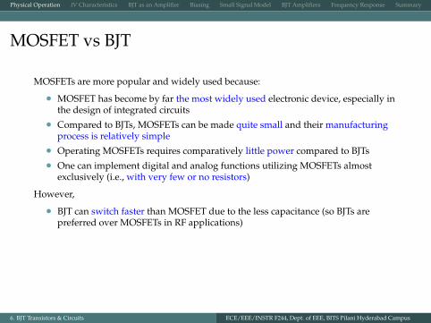
MOSFET vs BJT
MOSFETs are more popular and widely used because:
• MOSFET has become by far the most widely used electronic device, especially inthe design of integrated circuits
• Compared to BJTs, MOSFETs can be made quite small and their manufacturingprocess is relatively simple
• Operating MOSFETs requires comparatively little power compared to BJTs• One can implement digital and analog functions utilizing MOSFETs almost
exclusively (i.e., with very few or no resistors)
However,
• BJT can switch faster than MOSFET due to the less capacitance (so BJTs arepreferred over MOSFETs in RF applications)
• BJTs have high voltage gain• the reliability of BJT circuits under severe environmental conditions (e.g.,
automotive applications)• BJTs are Cheaper and they do not get damaged by static robust
6. BJT Transistors & Circuits ECE/EEE/INSTR F244, Dept. of EEE, BITS Pilani Hyderabad Campus

Physical Operation IV Characteristics BJT as an Amplifier Biasing Small Signal Model BJT Amplifiers Frequency Response Summary
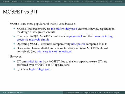
MOSFET vs BJT
MOSFETs are more popular and widely used because:
• MOSFET has become by far the most widely used electronic device, especially inthe design of integrated circuits
• Compared to BJTs, MOSFETs can be made quite small and their manufacturingprocess is relatively simple
• Operating MOSFETs requires comparatively little power compared to BJTs• One can implement digital and analog functions utilizing MOSFETs almost
exclusively (i.e., with very few or no resistors)
However,
• BJT can switch faster than MOSFET due to the less capacitance (so BJTs arepreferred over MOSFETs in RF applications)
• BJTs have high voltage gain• the reliability of BJT circuits under severe environmental conditions (e.g.,
automotive applications)• BJTs are Cheaper and they do not get damaged by static robust
6. BJT Transistors & Circuits ECE/EEE/INSTR F244, Dept. of EEE, BITS Pilani Hyderabad Campus
Physical Operation IV Characteristics BJT as an Amplifier Biasing Small Signal Model BJT Amplifiers Frequency Response Summary
MOSFET vs BJT
MOSFETs are more popular and widely used because:
• MOSFET has become by far the most widely used electronic device, especially inthe design of integrated circuits
• Compared to BJTs, MOSFETs can be made quite small and their manufacturingprocess is relatively simple
• Operating MOSFETs requires comparatively little power compared to BJTs• One can implement digital and analog functions utilizing MOSFETs almost
exclusively (i.e., with very few or no resistors)
However,
• BJT can switch faster than MOSFET due to the less capacitance (so BJTs arepreferred over MOSFETs in RF applications)
• BJTs have high voltage gain• the reliability of BJT circuits under severe environmental conditions (e.g.,
automotive applications)• BJTs are Cheaper and they do not get damaged by static robust
6. BJT Transistors & Circuits ECE/EEE/INSTR F244, Dept. of EEE, BITS Pilani Hyderabad Campus
Physical Operation IV Characteristics BJT as an Amplifier Biasing Small Signal Model BJT Amplifiers Frequency Response Summary
MOSFET vs BJT
MOSFETs are more popular and widely used because:
• MOSFET has become by far the most widely used electronic device, especially inthe design of integrated circuits
• Compared to BJTs, MOSFETs can be made quite small and their manufacturingprocess is relatively simple
• Operating MOSFETs requires comparatively little power compared to BJTs
• One can implement digital and analog functions utilizing MOSFETs almostexclusively (i.e., with very few or no resistors)
However,
• BJT can switch faster than MOSFET due to the less capacitance (so BJTs arepreferred over MOSFETs in RF applications)
• BJTs have high voltage gain• the reliability of BJT circuits under severe environmental conditions (e.g.,
automotive applications)• BJTs are Cheaper and they do not get damaged by static robust
6. BJT Transistors & Circuits ECE/EEE/INSTR F244, Dept. of EEE, BITS Pilani Hyderabad Campus
Physical Operation IV Characteristics BJT as an Amplifier Biasing Small Signal Model BJT Amplifiers Frequency Response Summary
MOSFET vs BJT
MOSFETs are more popular and widely used because:
• MOSFET has become by far the most widely used electronic device, especially inthe design of integrated circuits
• Compared to BJTs, MOSFETs can be made quite small and their manufacturingprocess is relatively simple
• Operating MOSFETs requires comparatively little power compared to BJTs• One can implement digital and analog functions utilizing MOSFETs almost
exclusively (i.e., with very few or no resistors)
However,
• BJT can switch faster than MOSFET due to the less capacitance (so BJTs arepreferred over MOSFETs in RF applications)
• BJTs have high voltage gain• the reliability of BJT circuits under severe environmental conditions (e.g.,
automotive applications)• BJTs are Cheaper and they do not get damaged by static robust
6. BJT Transistors & Circuits ECE/EEE/INSTR F244, Dept. of EEE, BITS Pilani Hyderabad Campus
Physical Operation IV Characteristics BJT as an Amplifier Biasing Small Signal Model BJT Amplifiers Frequency Response Summary
MOSFET vs BJT
MOSFETs are more popular and widely used because:
• MOSFET has become by far the most widely used electronic device, especially inthe design of integrated circuits
• Compared to BJTs, MOSFETs can be made quite small and their manufacturingprocess is relatively simple
• Operating MOSFETs requires comparatively little power compared to BJTs• One can implement digital and analog functions utilizing MOSFETs almost
exclusively (i.e., with very few or no resistors)
However,
• BJT can switch faster than MOSFET due to the less capacitance (so BJTs arepreferred over MOSFETs in RF applications)
• BJTs have high voltage gain
• the reliability of BJT circuits under severe environmental conditions (e.g.,automotive applications)
• BJTs are Cheaper and they do not get damaged by static robust
6. BJT Transistors & Circuits ECE/EEE/INSTR F244, Dept. of EEE, BITS Pilani Hyderabad Campus

Physical Operation IV Characteristics BJT as an Amplifier Biasing Small Signal Model BJT Amplifiers Frequency Response Summary
MOSFET vs BJT
MOSFETs are more popular and widely used because:
• MOSFET has become by far the most widely used electronic device, especially inthe design of integrated circuits
• Compared to BJTs, MOSFETs can be made quite small and their manufacturingprocess is relatively simple
• Operating MOSFETs requires comparatively little power compared to BJTs• One can implement digital and analog functions utilizing MOSFETs almost
exclusively (i.e., with very few or no resistors)
However,
• BJT can switch faster than MOSFET due to the less capacitance (so BJTs arepreferred over MOSFETs in RF applications)
• BJTs have high voltage gain• the reliability of BJT circuits under severe environmental conditions (e.g.,
automotive applications)
• BJTs are Cheaper and they do not get damaged by static robust
6. BJT Transistors & Circuits ECE/EEE/INSTR F244, Dept. of EEE, BITS Pilani Hyderabad Campus

Physical Operation IV Characteristics BJT as an Amplifier Biasing Small Signal Model BJT Amplifiers Frequency Response Summary
MOSFET vs BJT
MOSFETs are more popular and widely used because:
• MOSFET has become by far the most widely used electronic device, especially inthe design of integrated circuits
• Compared to BJTs, MOSFETs can be made quite small and their manufacturingprocess is relatively simple
• Operating MOSFETs requires comparatively little power compared to BJTs• One can implement digital and analog functions utilizing MOSFETs almost
exclusively (i.e., with very few or no resistors)
However,
• BJT can switch faster than MOSFET due to the less capacitance (so BJTs arepreferred over MOSFETs in RF applications)
• BJTs have high voltage gain• the reliability of BJT circuits under severe environmental conditions (e.g.,
automotive applications)• BJTs are Cheaper and they do not get damaged by static robust
6. BJT Transistors & Circuits ECE/EEE/INSTR F244, Dept. of EEE, BITS Pilani Hyderabad Campus

Physical Operation IV Characteristics BJT as an Amplifier Biasing Small Signal Model BJT Amplifiers Frequency Response Summary
BiCMOS
Bipolar transistors can be combined with MOSFETs to create innovative circuits thattake advantage of the high-input-impedance and low-power operation of MOSFETs
and the very-high-frequency operation and high-current-driving capability of bipolartransistors.
The resulting technology is known as BiCMOS, and it is finding increasingly largerareas of application.
6. BJT Transistors & Circuits ECE/EEE/INSTR F244, Dept. of EEE, BITS Pilani Hyderabad Campus

Physical Operation IV Characteristics BJT as an Amplifier Biasing Small Signal Model BJT Amplifiers Frequency Response Summary
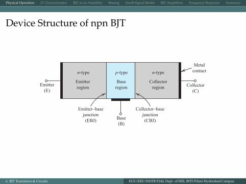
Device Structure of npn BJT
n-type n-type
Emitterregion
Emitter–basejunction(EBJ)
Collector–basejunction(CBJ)
Collector(C)
Emitter(E)
Metalcontact
Collectorregion
p-type
Baseregion
Base(B)
6. BJT Transistors & Circuits ECE/EEE/INSTR F244, Dept. of EEE, BITS Pilani Hyderabad Campus
Physical Operation IV Characteristics BJT as an Amplifier Biasing Small Signal Model BJT Amplifiers Frequency Response Summary
Device Structure of npn BJT
n-type n-type
Emitterregion
Emitter–basejunction(EBJ)
Collector–basejunction(CBJ)
Collector(C)
Emitter(E)
Metalcontact
Collectorregion
p-type
Baseregion
Base(B)
6. BJT Transistors & Circuits ECE/EEE/INSTR F244, Dept. of EEE, BITS Pilani Hyderabad Campus

Physical Operation IV Characteristics BJT as an Amplifier Biasing Small Signal Model BJT Amplifiers Frequency Response Summary
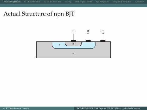
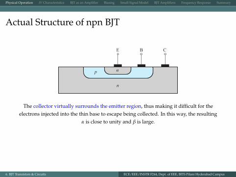
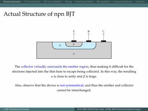
Actual Structure of npn BJT
E B C
n
np
The collector virtually surrounds the emitter region, thus making it difficult for theelectrons injected into the thin base to escape being collected. In this way, the resulting
α is close to unity and β is large.
Also, observe that the device is not symmetrical, and thus the emitter and collectorcannot be interchanged.
6. BJT Transistors & Circuits ECE/EEE/INSTR F244, Dept. of EEE, BITS Pilani Hyderabad Campus
Physical Operation IV Characteristics BJT as an Amplifier Biasing Small Signal Model BJT Amplifiers Frequency Response Summary
Operation of BJT
6. BJT Transistors & Circuits ECE/EEE/INSTR F244, Dept. of EEE, BITS Pilani Hyderabad Campus
Physical Operation IV Characteristics BJT as an Amplifier Biasing Small Signal Model BJT Amplifiers Frequency Response Summary
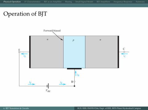
Operation of BJT
B
C
iEiE
iCiE
E
Forward-biased
n p n
VBE
iB
6. BJT Transistors & Circuits ECE/EEE/INSTR F244, Dept. of EEE, BITS Pilani Hyderabad Campus
Physical Operation IV Characteristics BJT as an Amplifier Biasing Small Signal Model BJT Amplifiers Frequency Response Summary
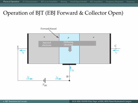
Operation of BJT (EBJ Forward & Collector Open)
B
C
iEiE
iCiE
E
Forward-biased
n p n
VBE
Injectedelectrons
Diffusingelectrons
iB
6. BJT Transistors & Circuits ECE/EEE/INSTR F244, Dept. of EEE, BITS Pilani Hyderabad Campus
Physical Operation IV Characteristics BJT as an Amplifier Biasing Small Signal Model BJT Amplifiers Frequency Response Summary
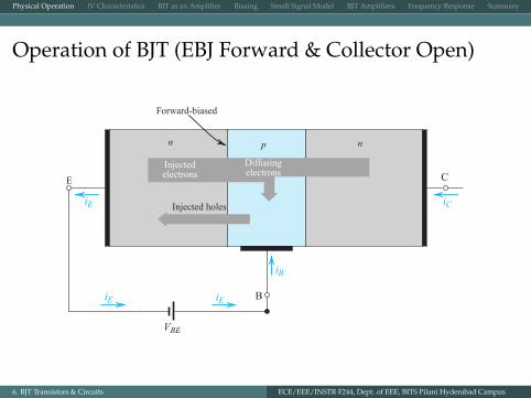
Operation of BJT (EBJ Forward & Collector Open)
B
C
iEiE
iCiE Injected holes
E
Forward-biased
n p n
VBE
Injectedelectrons
Diffusingelectrons
iB
6. BJT Transistors & Circuits ECE/EEE/INSTR F244, Dept. of EEE, BITS Pilani Hyderabad Campus
Physical Operation IV Characteristics BJT as an Amplifier Biasing Small Signal Model BJT Amplifiers Frequency Response Summary
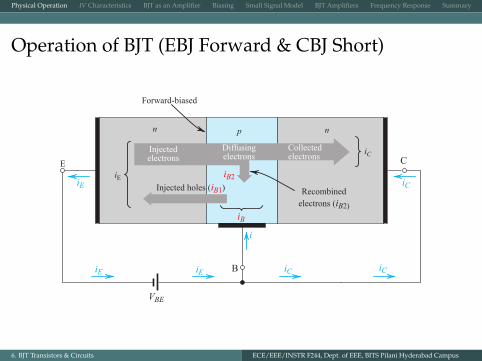
Operation of BJT (EBJ Forward & CBJ Short)
B
C
iEiE iC iC
i
iB
iB2iCiE
Recombinedelectrons (iB2)
Injected holes (iB1
E
Forward-biased
iE
iC
n p n
VBE
(
Injectedelectrons
Diffusingelectrons
Collectedelectrons
6. BJT Transistors & Circuits ECE/EEE/INSTR F244, Dept. of EEE, BITS Pilani Hyderabad Campus
Physical Operation IV Characteristics BJT as an Amplifier Biasing Small Signal Model BJT Amplifiers Frequency Response Summary
Operation of BJT (EBJ Forward & CBJ Short)
B
C
iEiE iC iC
i
iB
iB2iCiE
Recombinedelectrons (iB2)
Injected holes (iB1
E
Forward-biased
iE
iC
n p n
Accelerated through the depletion region
VBE
(
Injectedelectrons
Diffusingelectrons
Collectedelectrons
6. BJT Transistors & Circuits ECE/EEE/INSTR F244, Dept. of EEE, BITS Pilani Hyderabad Campus
Physical Operation IV Characteristics BJT as an Amplifier Biasing Small Signal Model BJT Amplifiers Frequency Response Summary
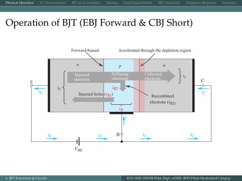
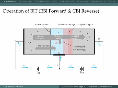
Operation of BJT (EBJ Forward & CBJ Reverse)
B
C
iEiE iC iC
i
iB
iB2iCiE
Recombinedelectrons (iB2)
Injected holes (iB1
E
Forward-biased
iE
iC
n p n
Accelerated through the depletion region
VBE
(
Injectedelectrons
Diffusingelectrons
Collectedelectrons
VCB
6. BJT Transistors & Circuits ECE/EEE/INSTR F244, Dept. of EEE, BITS Pilani Hyderabad Campus

Physical Operation IV Characteristics BJT as an Amplifier Biasing Small Signal Model BJT Amplifiers Frequency Response Summary
Operation of BJT (EBJ Forward & CBJ More Reverse)
B
C
iEiE iC iC
i
iB
iB2iCiE
Recombinedelectrons (iB2)
Injected holes (iB1
E
Forward-biased
iE
iC
n p n
Accelerated through the depletion region
VBE
(
Injectedelectrons
Diffusingelectrons
Collectedelectrons
VCB
6. BJT Transistors & Circuits ECE/EEE/INSTR F244, Dept. of EEE, BITS Pilani Hyderabad Campus
Physical Operation IV Characteristics BJT as an Amplifier Biasing Small Signal Model BJT Amplifiers Frequency Response Summary
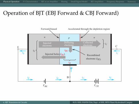
Operation of BJT (EBJ Forward & CBJ Forward)
B
C
iEiE iC iC
i
iB
iB2iCiE
Recombinedelectrons (iB2)
Injected holes (iB1
E
Forward-biased
iE
iC
n p n
Accelerated through the depletion region
VBE
(
Injectedelectrons
Diffusingelectrons
Collectedelectrons
VCB
6. BJT Transistors & Circuits ECE/EEE/INSTR F244, Dept. of EEE, BITS Pilani Hyderabad Campus
Physical Operation IV Characteristics BJT as an Amplifier Biasing Small Signal Model BJT Amplifiers Frequency Response Summary
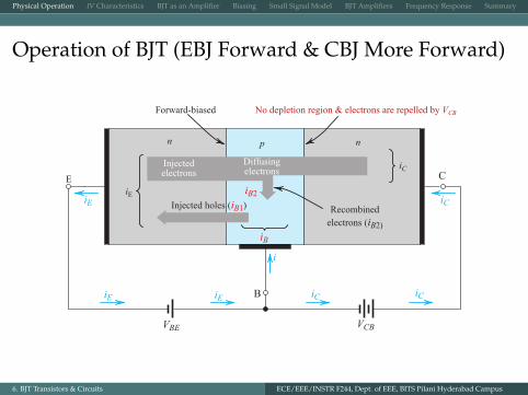
Operation of BJT (EBJ Forward & CBJ More Forward)
B
C
iEiE iC iC
i
iB
iB2iCiE
Recombinedelectrons (iB2)
Injected holes (iB1
E
Forward-biased
iE
iC
n p n
No depletion region & electrons are repelled by VCB
VBE
(
Injectedelectrons
Diffusingelectrons
VCB
6. BJT Transistors & Circuits ECE/EEE/INSTR F244, Dept. of EEE, BITS Pilani Hyderabad Campus

Physical Operation IV Characteristics BJT as an Amplifier Biasing Small Signal Model BJT Amplifiers Frequency Response Summary
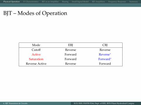
BJT – Modes of Operation
Mode EBJ CBJ
Cutoff Reverse ReverseActive Forward Reverse∗
Saturation Forward Forward∗
Reverse Active Reverse Forward
6. BJT Transistors & Circuits ECE/EEE/INSTR F244, Dept. of EEE, BITS Pilani Hyderabad Campus
Physical Operation IV Characteristics BJT as an Amplifier Biasing Small Signal Model BJT Amplifiers Frequency Response Summary
BJT – Modes of Operation
Mode EBJ CBJ
Cutoff Reverse ReverseActive Forward Reverse∗
Saturation Forward Forward∗
Reverse Active Reverse Forward
6. BJT Transistors & Circuits ECE/EEE/INSTR F244, Dept. of EEE, BITS Pilani Hyderabad Campus

Physical Operation IV Characteristics BJT as an Amplifier Biasing Small Signal Model BJT Amplifiers Frequency Response Summary
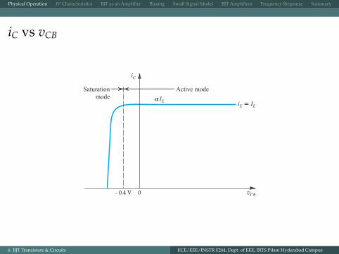
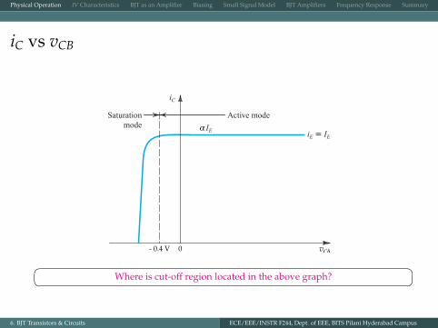
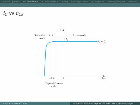
iC vs vCB
vCB
Saturationmode
Active mode
α IE iE= IE
- 0.4 V
iC
0�� ��Where is cut-off region located in the above graph?
6. BJT Transistors & Circuits ECE/EEE/INSTR F244, Dept. of EEE, BITS Pilani Hyderabad Campus
Physical Operation IV Characteristics BJT as an Amplifier Biasing Small Signal Model BJT Amplifiers Frequency Response Summary
iC vs vCB
vCB
Saturationmode
Active mode
α IE iE= IE
- 0.4 V
iC
0
�� ��Where is cut-off region located in the above graph?
6. BJT Transistors & Circuits ECE/EEE/INSTR F244, Dept. of EEE, BITS Pilani Hyderabad Campus
Physical Operation IV Characteristics BJT as an Amplifier Biasing Small Signal Model BJT Amplifiers Frequency Response Summary
iC vs vCB
vCB
Saturationmode
Active mode
α IE iE= IE
- 0.4 V
iC
0�� ��Where is cut-off region located in the above graph?
6. BJT Transistors & Circuits ECE/EEE/INSTR F244, Dept. of EEE, BITS Pilani Hyderabad Campus
Physical Operation IV Characteristics BJT as an Amplifier Biasing Small Signal Model BJT Amplifiers Frequency Response Summary
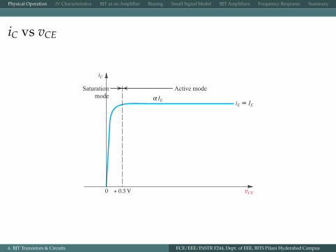
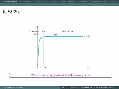
iC vs vCE
vCE
Saturationmode
Active mode
α IE iE= IE
+ 0.3 V
iC
0
�� ��Where is cut-off region located in the above graph?
6. BJT Transistors & Circuits ECE/EEE/INSTR F244, Dept. of EEE, BITS Pilani Hyderabad Campus
Physical Operation IV Characteristics BJT as an Amplifier Biasing Small Signal Model BJT Amplifiers Frequency Response Summary
iC vs vCE
vCE
Saturationmode
Active mode
α IE iE= IE
+ 0.3 V
iC
0�� ��Where is cut-off region located in the above graph?
6. BJT Transistors & Circuits ECE/EEE/INSTR F244, Dept. of EEE, BITS Pilani Hyderabad Campus

Physical Operation IV Characteristics BJT as an Amplifier Biasing Small Signal Model BJT Amplifiers Frequency Response Summary
Since BJT can be visualized as a combination of two pn junction diodes, let’srecap the theory of pn junction diode ...
6. BJT Transistors & Circuits ECE/EEE/INSTR F244, Dept. of EEE, BITS Pilani Hyderabad Campus

Physical Operation IV Characteristics BJT as an Amplifier Biasing Small Signal Model BJT Amplifiers Frequency Response Summary
Minority Carrier Injection & Recombination
6. BJT Transistors & Circuits ECE/EEE/INSTR F244, Dept. of EEE, BITS Pilani Hyderabad Campus

Physical Operation IV Characteristics BJT as an Amplifier Biasing Small Signal Model BJT Amplifiers Frequency Response Summary
Minority Carrier Injection & Recombination
0
n regionp region
x
6. BJT Transistors & Circuits ECE/EEE/INSTR F244, Dept. of EEE, BITS Pilani Hyderabad Campus

Physical Operation IV Characteristics BJT as an Amplifier Biasing Small Signal Model BJT Amplifiers Frequency Response Summary
Minority Carrier Injection & Recombination
0
n regionp region
pn, np
x
6. BJT Transistors & Circuits ECE/EEE/INSTR F244, Dept. of EEE, BITS Pilani Hyderabad Campus

Physical Operation IV Characteristics BJT as an Amplifier Biasing Small Signal Model BJT Amplifiers Frequency Response Summary
Minority Carrier Injection & Recombination
0
Depletionregion
n regionp region
pn, np
-xp xn x
6. BJT Transistors & Circuits ECE/EEE/INSTR F244, Dept. of EEE, BITS Pilani Hyderabad Campus
Physical Operation IV Characteristics BJT as an Amplifier Biasing Small Signal Model BJT Amplifiers Frequency Response Summary
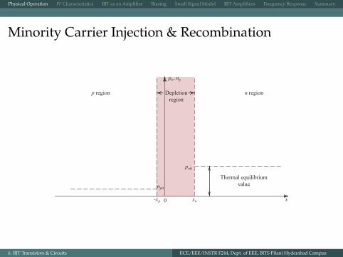
Minority Carrier Injection & Recombination
0
Depletionregion
n region
Thermal equilibriumvalue
p region
pn0
pn, np
np0
-xp xn x
6. BJT Transistors & Circuits ECE/EEE/INSTR F244, Dept. of EEE, BITS Pilani Hyderabad Campus
Physical Operation IV Characteristics BJT as an Amplifier Biasing Small Signal Model BJT Amplifiers Frequency Response Summary
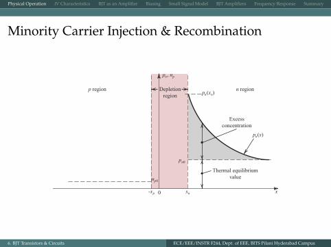
Minority Carrier Injection & Recombination
0
Depletionregion
n region
Excessconcentration
Thermal equilibriumvalue
p regionpn
pn0
(xn)
pn(x)
pn, np
np0
-xp xn x
6. BJT Transistors & Circuits ECE/EEE/INSTR F244, Dept. of EEE, BITS Pilani Hyderabad Campus
Physical Operation IV Characteristics BJT as an Amplifier Biasing Small Signal Model BJT Amplifiers Frequency Response Summary
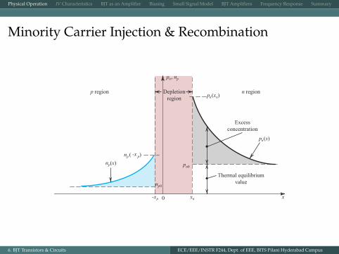
Minority Carrier Injection & Recombination
0
Depletionregion
n region
Excessconcentration
Thermal equilibriumvalue
p regionpn
pn0
(xn)
pn(x)
pn, np
np
np0
( p)
-xp xn x
np(x)
-x
6. BJT Transistors & Circuits ECE/EEE/INSTR F244, Dept. of EEE, BITS Pilani Hyderabad Campus

Physical Operation IV Characteristics BJT as an Amplifier Biasing Small Signal Model BJT Amplifiers Frequency Response Summary
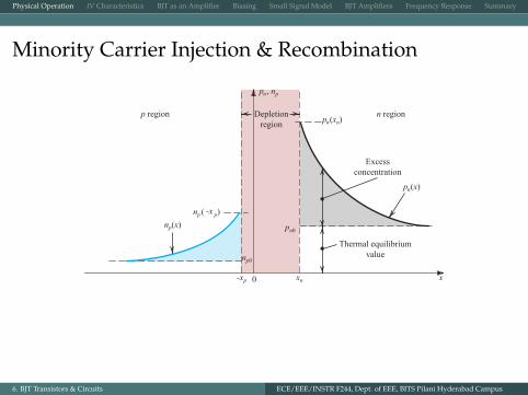
Minority Carrier Injection & Recombination
0
Depletionregion
n region
Excessconcentration
Thermal equilibriumvalue
p regionpn
pn0
(xn)
pn(x)
pn, np
np
np0
( p)
-xp xn x
np(x)
-x
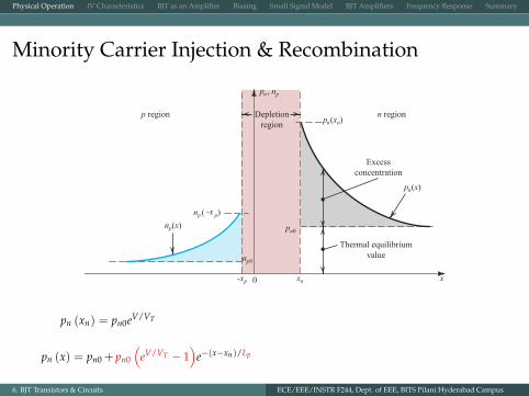
pn (xn) = pn0eV/VT
pn (x) = pn0 + pn0
(eV/VT − 1
)e−(x−xn)/Lp
Jp (xn) = −qDpdpn (x)
dx
∣∣∣∣x=xn
=qDppn0
Lp
(eV/VT − 1
)
6. BJT Transistors & Circuits ECE/EEE/INSTR F244, Dept. of EEE, BITS Pilani Hyderabad Campus
Physical Operation IV Characteristics BJT as an Amplifier Biasing Small Signal Model BJT Amplifiers Frequency Response Summary
Minority Carrier Injection & Recombination
0
Depletionregion
n region
Excessconcentration
Thermal equilibriumvalue
p regionpn
pn0
(xn)
pn(x)
pn, np
np
np0
( p)
-xp xn x
np(x)
-x
pn (xn) = pn0eV/VT
pn (x) = pn0 + pn0
(eV/VT − 1
)e−(x−xn)/Lp
Jp (xn) = −qDpdpn (x)
dx
∣∣∣∣x=xn
=qDppn0
Lp
(eV/VT − 1
)
6. BJT Transistors & Circuits ECE/EEE/INSTR F244, Dept. of EEE, BITS Pilani Hyderabad Campus

Physical Operation IV Characteristics BJT as an Amplifier Biasing Small Signal Model BJT Amplifiers Frequency Response Summary
In this chapter, we are more interested in active mode because of it’samplification property ... So, let’s derive the expressions for various currents
in active mode ...
6. BJT Transistors & Circuits ECE/EEE/INSTR F244, Dept. of EEE, BITS Pilani Hyderabad Campus

Physical Operation IV Characteristics BJT as an Amplifier Biasing Small Signal Model BJT Amplifiers Frequency Response Summary
Minority Carrier Concentrations (Active Mode)
Emitter(n)
EBJdepletion
region
Base(p)
CBJdepletion
region
Collector(n)
Car
rier
con
cent
rati
on
Holeconcentration
Effective basewidth W
Distance (x)
np (0)
Electronconcentrationnp (ideal)
np (withrecombination)
pn (0)pn0
np (0) = np0evBE/VT (1)
6. BJT Transistors & Circuits ECE/EEE/INSTR F244, Dept. of EEE, BITS Pilani Hyderabad Campus

Physical Operation IV Characteristics BJT as an Amplifier Biasing Small Signal Model BJT Amplifiers Frequency Response Summary
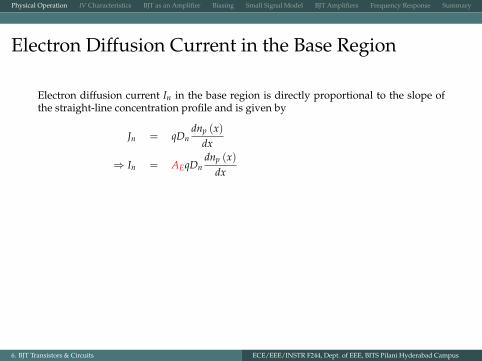
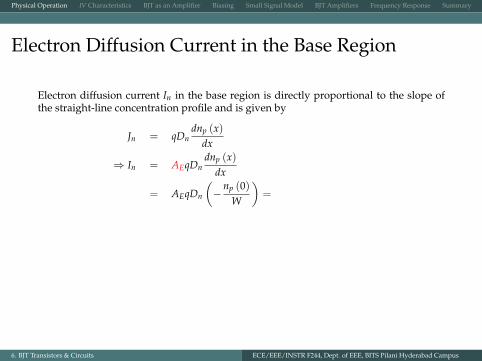
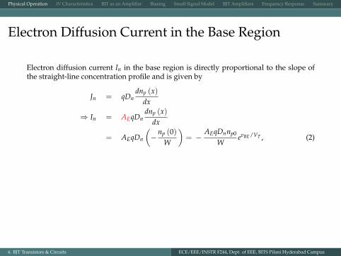
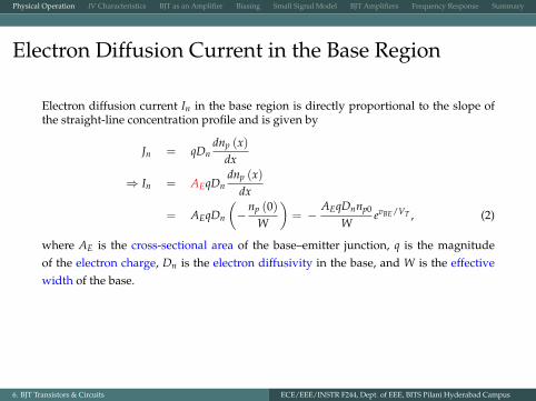
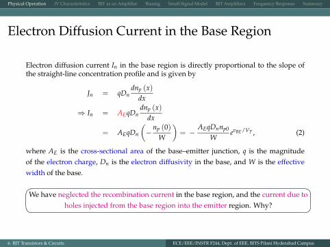
Electron Diffusion Current in the Base Region
Electron diffusion current In in the base region is directly proportional to the slope ofthe straight-line concentration profile and is given by
Jn = qDndnp (x)
dx
⇒ In = AEqDndnp (x)
dx
= AEqDn
(−
np (0)W
)= −
AEqDnnp0
WevBE/VT , (2)
where AE is the cross-sectional area of the base–emitter junction, q is the magnitudeof the electron charge, Dn is the electron diffusivity in the base, and W is the effectivewidth of the base.�
�We have neglected the recombination current in the base region, and the current due to
holes injected from the base region into the emitter region. Why?
6. BJT Transistors & Circuits ECE/EEE/INSTR F244, Dept. of EEE, BITS Pilani Hyderabad Campus
Physical Operation IV Characteristics BJT as an Amplifier Biasing Small Signal Model BJT Amplifiers Frequency Response Summary
Electron Diffusion Current in the Base Region
Electron diffusion current In in the base region is directly proportional to the slope ofthe straight-line concentration profile and is given by
Jn = qDndnp (x)
dx
⇒ In = AEqDndnp (x)
dx
= AEqDn
(−
np (0)W
)= −
AEqDnnp0
WevBE/VT , (2)
where AE is the cross-sectional area of the base–emitter junction, q is the magnitudeof the electron charge, Dn is the electron diffusivity in the base, and W is the effectivewidth of the base.�
�We have neglected the recombination current in the base region, and the current due to
holes injected from the base region into the emitter region. Why?
6. BJT Transistors & Circuits ECE/EEE/INSTR F244, Dept. of EEE, BITS Pilani Hyderabad Campus
Physical Operation IV Characteristics BJT as an Amplifier Biasing Small Signal Model BJT Amplifiers Frequency Response Summary
Electron Diffusion Current in the Base Region
Electron diffusion current In in the base region is directly proportional to the slope ofthe straight-line concentration profile and is given by
Jn = qDndnp (x)
dx
⇒ In = AEqDndnp (x)
dx
= AEqDn
(−
np (0)W
)=
−AEqDnnp0
WevBE/VT , (2)
where AE is the cross-sectional area of the base–emitter junction, q is the magnitudeof the electron charge, Dn is the electron diffusivity in the base, and W is the effectivewidth of the base.�
�We have neglected the recombination current in the base region, and the current due to
holes injected from the base region into the emitter region. Why?
6. BJT Transistors & Circuits ECE/EEE/INSTR F244, Dept. of EEE, BITS Pilani Hyderabad Campus
Physical Operation IV Characteristics BJT as an Amplifier Biasing Small Signal Model BJT Amplifiers Frequency Response Summary
Electron Diffusion Current in the Base Region
Electron diffusion current In in the base region is directly proportional to the slope ofthe straight-line concentration profile and is given by
Jn = qDndnp (x)
dx
⇒ In = AEqDndnp (x)
dx
= AEqDn
(−
np (0)W
)= −
AEqDnnp0
WevBE/VT , (2)
where AE is the cross-sectional area of the base–emitter junction, q is the magnitudeof the electron charge, Dn is the electron diffusivity in the base, and W is the effectivewidth of the base.�
�We have neglected the recombination current in the base region, and the current due to
holes injected from the base region into the emitter region. Why?
6. BJT Transistors & Circuits ECE/EEE/INSTR F244, Dept. of EEE, BITS Pilani Hyderabad Campus
Physical Operation IV Characteristics BJT as an Amplifier Biasing Small Signal Model BJT Amplifiers Frequency Response Summary
Electron Diffusion Current in the Base Region
Electron diffusion current In in the base region is directly proportional to the slope ofthe straight-line concentration profile and is given by
Jn = qDndnp (x)
dx
⇒ In = AEqDndnp (x)
dx
= AEqDn
(−
np (0)W
)= −
AEqDnnp0
WevBE/VT , (2)
where AE is the cross-sectional area of the base–emitter junction, q is the magnitudeof the electron charge, Dn is the electron diffusivity in the base, and W is the effectivewidth of the base.
�
�We have neglected the recombination current in the base region, and the current due to
holes injected from the base region into the emitter region. Why?
6. BJT Transistors & Circuits ECE/EEE/INSTR F244, Dept. of EEE, BITS Pilani Hyderabad Campus
Physical Operation IV Characteristics BJT as an Amplifier Biasing Small Signal Model BJT Amplifiers Frequency Response Summary
Electron Diffusion Current in the Base Region
Electron diffusion current In in the base region is directly proportional to the slope ofthe straight-line concentration profile and is given by
Jn = qDndnp (x)
dx
⇒ In = AEqDndnp (x)
dx
= AEqDn
(−
np (0)W
)= −
AEqDnnp0
WevBE/VT , (2)
where AE is the cross-sectional area of the base–emitter junction, q is the magnitudeof the electron charge, Dn is the electron diffusivity in the base, and W is the effectivewidth of the base.�
�We have neglected the recombination current in the base region, and the current due to
holes injected from the base region into the emitter region. Why?
6. BJT Transistors & Circuits ECE/EEE/INSTR F244, Dept. of EEE, BITS Pilani Hyderabad Campus

Physical Operation IV Characteristics BJT as an Amplifier Biasing Small Signal Model BJT Amplifiers Frequency Response Summary
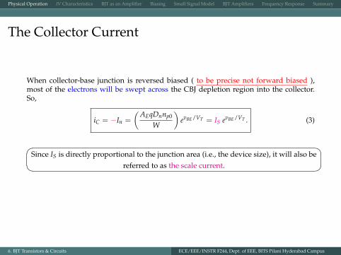
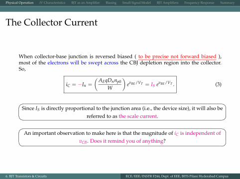
The Collector Current
When collector-base junction is reversed biased ( to be precise not forward biased ),most of the electrons will be swept across the CBJ depletion region into the collector.So,
iC = −In =
(AEqDnnp0
W
)evBE/VT = IS evBE/VT . (3)
�
�Since IS is directly proportional to the junction area (i.e., the device size), it will also be
referred to as the scale current.�
�An important observation to make here is that the magnitude of iC is independent of
vCB. Does it remind you of anything?
6. BJT Transistors & Circuits ECE/EEE/INSTR F244, Dept. of EEE, BITS Pilani Hyderabad Campus

Physical Operation IV Characteristics BJT as an Amplifier Biasing Small Signal Model BJT Amplifiers Frequency Response Summary
The Collector Current
When collector-base junction is reversed biased ( to be precise not forward biased ),most of the electrons will be swept across the CBJ depletion region into the collector.So,
iC = −In =
(AEqDnnp0
W
)evBE/VT = IS evBE/VT . (3)
�
�Since IS is directly proportional to the junction area (i.e., the device size), it will also be
referred to as the scale current.�
�An important observation to make here is that the magnitude of iC is independent of
vCB. Does it remind you of anything?
6. BJT Transistors & Circuits ECE/EEE/INSTR F244, Dept. of EEE, BITS Pilani Hyderabad Campus
Physical Operation IV Characteristics BJT as an Amplifier Biasing Small Signal Model BJT Amplifiers Frequency Response Summary
The Collector Current
When collector-base junction is reversed biased ( to be precise not forward biased ),most of the electrons will be swept across the CBJ depletion region into the collector.So,
iC = −In =
(AEqDnnp0
W
)evBE/VT = IS evBE/VT . (3)
�
�Since IS is directly proportional to the junction area (i.e., the device size), it will also be
referred to as the scale current.
�
�An important observation to make here is that the magnitude of iC is independent of
vCB. Does it remind you of anything?
6. BJT Transistors & Circuits ECE/EEE/INSTR F244, Dept. of EEE, BITS Pilani Hyderabad Campus
Physical Operation IV Characteristics BJT as an Amplifier Biasing Small Signal Model BJT Amplifiers Frequency Response Summary
The Collector Current
When collector-base junction is reversed biased ( to be precise not forward biased ),most of the electrons will be swept across the CBJ depletion region into the collector.So,
iC = −In =
(AEqDnnp0
W
)evBE/VT = IS evBE/VT . (3)
�
�Since IS is directly proportional to the junction area (i.e., the device size), it will also be
referred to as the scale current.�
�An important observation to make here is that the magnitude of iC is independent of
vCB. Does it remind you of anything?
6. BJT Transistors & Circuits ECE/EEE/INSTR F244, Dept. of EEE, BITS Pilani Hyderabad Campus

Physical Operation IV Characteristics BJT as an Amplifier Biasing Small Signal Model BJT Amplifiers Frequency Response Summary
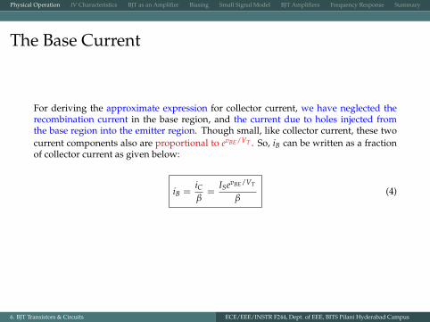
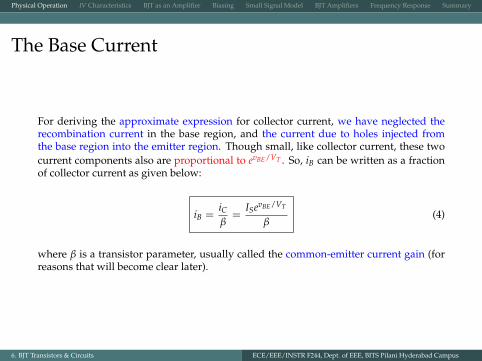
The Base Current
For deriving the approximate expression for collector current, we have neglected therecombination current in the base region, and the current due to holes injected fromthe base region into the emitter region. Though small, like collector current, these twocurrent components also are proportional to evBE/VT . So, iB can be written as a fractionof collector current as given below:
iB =iCβ
=ISevBE/VT
β(4)
where β is a transistor parameter, usually called the common-emitter current gain (forreasons that will become clear later).
6. BJT Transistors & Circuits ECE/EEE/INSTR F244, Dept. of EEE, BITS Pilani Hyderabad Campus

Physical Operation IV Characteristics BJT as an Amplifier Biasing Small Signal Model BJT Amplifiers Frequency Response Summary
The Base Current
For deriving the approximate expression for collector current, we have neglected therecombination current in the base region, and the current due to holes injected fromthe base region into the emitter region.
Though small, like collector current, these twocurrent components also are proportional to evBE/VT . So, iB can be written as a fractionof collector current as given below:
iB =iCβ
=ISevBE/VT
β(4)
where β is a transistor parameter, usually called the common-emitter current gain (forreasons that will become clear later).
6. BJT Transistors & Circuits ECE/EEE/INSTR F244, Dept. of EEE, BITS Pilani Hyderabad Campus

Physical Operation IV Characteristics BJT as an Amplifier Biasing Small Signal Model BJT Amplifiers Frequency Response Summary
The Base Current
For deriving the approximate expression for collector current, we have neglected therecombination current in the base region, and the current due to holes injected fromthe base region into the emitter region. Though small, like collector current, these twocurrent components also are proportional to evBE/VT .
So, iB can be written as a fractionof collector current as given below:
iB =iCβ
=ISevBE/VT
β(4)
where β is a transistor parameter, usually called the common-emitter current gain (forreasons that will become clear later).
6. BJT Transistors & Circuits ECE/EEE/INSTR F244, Dept. of EEE, BITS Pilani Hyderabad Campus
Physical Operation IV Characteristics BJT as an Amplifier Biasing Small Signal Model BJT Amplifiers Frequency Response Summary
The Base Current
For deriving the approximate expression for collector current, we have neglected therecombination current in the base region, and the current due to holes injected fromthe base region into the emitter region. Though small, like collector current, these twocurrent components also are proportional to evBE/VT . So, iB can be written as a fractionof collector current as given below:
iB =iCβ
=ISevBE/VT
β(4)
where β is a transistor parameter, usually called the common-emitter current gain (forreasons that will become clear later).
6. BJT Transistors & Circuits ECE/EEE/INSTR F244, Dept. of EEE, BITS Pilani Hyderabad Campus
Physical Operation IV Characteristics BJT as an Amplifier Biasing Small Signal Model BJT Amplifiers Frequency Response Summary
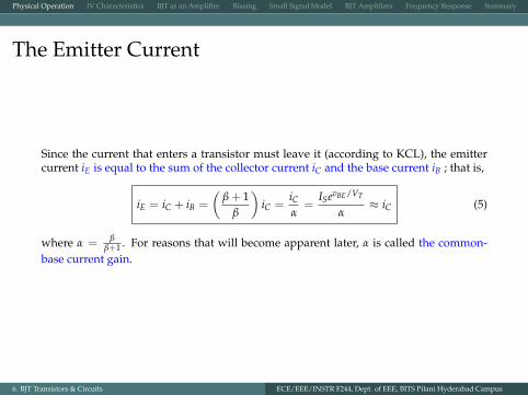
The Emitter Current
Since the current that enters a transistor must leave it (according to KCL), the emittercurrent
iE is equal to the sum of the collector current iC and the base current iB ;
that is,
iE = iC + iB =
(β + 1
β
)iC =
iCα
=ISevBE/VT
α≈ iC (5)
where α = ββ+1 . For reasons that will become apparent later, α is called the common-
base current gain.
6. BJT Transistors & Circuits ECE/EEE/INSTR F244, Dept. of EEE, BITS Pilani Hyderabad Campus
Physical Operation IV Characteristics BJT as an Amplifier Biasing Small Signal Model BJT Amplifiers Frequency Response Summary
The Emitter Current
Since the current that enters a transistor must leave it (according to KCL), the emittercurrent iE is equal to the sum of the collector current iC and the base current iB ;
that is,
iE = iC + iB =
(β + 1
β
)iC =
iCα
=ISevBE/VT
α≈ iC (5)
where α = ββ+1 . For reasons that will become apparent later, α is called the common-
base current gain.
6. BJT Transistors & Circuits ECE/EEE/INSTR F244, Dept. of EEE, BITS Pilani Hyderabad Campus
Physical Operation IV Characteristics BJT as an Amplifier Biasing Small Signal Model BJT Amplifiers Frequency Response Summary
The Emitter Current
Since the current that enters a transistor must leave it (according to KCL), the emittercurrent iE is equal to the sum of the collector current iC and the base current iB ; that is,
iE = iC + iB =
(β + 1
β
)iC =
iCα
=ISevBE/VT
α≈ iC (5)
where α = ββ+1 . For reasons that will become apparent later, α is called the common-
base current gain.
6. BJT Transistors & Circuits ECE/EEE/INSTR F244, Dept. of EEE, BITS Pilani Hyderabad Campus

Physical Operation IV Characteristics BJT as an Amplifier Biasing Small Signal Model BJT Amplifiers Frequency Response Summary
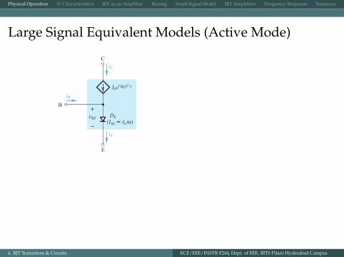
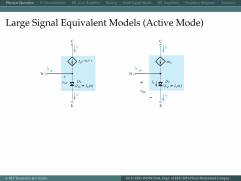
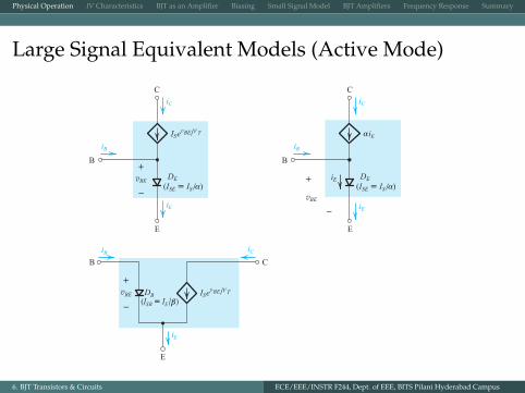
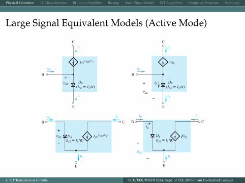
Large Signal Equivalent Models (Active Mode)
6. BJT Transistors & Circuits ECE/EEE/INSTR F244, Dept. of EEE, BITS Pilani Hyderabad Campus
Physical Operation IV Characteristics BJT as an Amplifier Biasing Small Signal Model BJT Amplifiers Frequency Response Summary
Large Signal Equivalent Models (Active Mode)
(ISE= IS α)
C
E
B
iB
iE
vBE DE
iC
ISevBE VT
+
6. BJT Transistors & Circuits ECE/EEE/INSTR F244, Dept. of EEE, BITS Pilani Hyderabad Campus
Physical Operation IV Characteristics BJT as an Amplifier Biasing Small Signal Model BJT Amplifiers Frequency Response Summary
Large Signal Equivalent Models (Active Mode)
C
E
B
(ISE= IS α)
C
E
B
iB
iE
vBE DE
iC
iB
iC
DEiE
vBE
iE
iE
ISevBE VT
+
(ISE= IS α)+
α
6. BJT Transistors & Circuits ECE/EEE/INSTR F244, Dept. of EEE, BITS Pilani Hyderabad Campus
Physical Operation IV Characteristics BJT as an Amplifier Biasing Small Signal Model BJT Amplifiers Frequency Response Summary
Large Signal Equivalent Models (Active Mode)
C
E
B
(ISE= IS α)
C
E
B
iB
iE
vBE DE
iC
iB
iC
DEiE
vBE
iE
iE
E
B C
iB
DB
iC
iE
vBE
ISevBE VT
+
(ISE= IS α)+
α
+ISe
vBE VT
(ISB= IS )β
6. BJT Transistors & Circuits ECE/EEE/INSTR F244, Dept. of EEE, BITS Pilani Hyderabad Campus
Physical Operation IV Characteristics BJT as an Amplifier Biasing Small Signal Model BJT Amplifiers Frequency Response Summary
Large Signal Equivalent Models (Active Mode)
C
E
B
(ISE= IS α)
C
E
B
iB
iE
vBE DE
iC
iB
iC
DEiE
vBE
iE
iE
E
B C
iB
DB
iC
iE
vBE
E
BiB
β iB
iEvBE
C
iCiB
DB
ISevBE VT
+
(ISE= IS α)+
α
+ (ISB= IS )β
+ISe
vBE VT
(ISB= IS )β
6. BJT Transistors & Circuits ECE/EEE/INSTR F244, Dept. of EEE, BITS Pilani Hyderabad Campus
Physical Operation IV Characteristics BJT as an Amplifier Biasing Small Signal Model BJT Amplifiers Frequency Response Summary
Active or Saturation Mode?
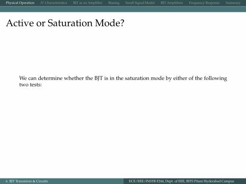
We can determine whether the BJT is in the saturation mode by either of the followingtwo tests:
1 Is the CBJ forward biased by more than 0.4 V?
2 Is the ratio iC/iB lower than β ?
6. BJT Transistors & Circuits ECE/EEE/INSTR F244, Dept. of EEE, BITS Pilani Hyderabad Campus
Physical Operation IV Characteristics BJT as an Amplifier Biasing Small Signal Model BJT Amplifiers Frequency Response Summary
Active or Saturation Mode?
We can determine whether the BJT is in the saturation mode by either of the followingtwo tests:
1 Is the CBJ forward biased by more than 0.4 V?
2 Is the ratio iC/iB lower than β ?
6. BJT Transistors & Circuits ECE/EEE/INSTR F244, Dept. of EEE, BITS Pilani Hyderabad Campus

Physical Operation IV Characteristics BJT as an Amplifier Biasing Small Signal Model BJT Amplifiers Frequency Response Summary
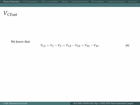
VCEsat
We know thatVCE = VC −VE = VCB −VEB = VBE −VBC. (6)
In saturation mode, both VBE and VBC are positive and VBC will be usually smaller thanVBE (because CBJ has a much larger area than the EBJ). Thus, in saturation mode,
VCEsat ≈ 0.1 to 0.3 V. (7)
6. BJT Transistors & Circuits ECE/EEE/INSTR F244, Dept. of EEE, BITS Pilani Hyderabad Campus
Physical Operation IV Characteristics BJT as an Amplifier Biasing Small Signal Model BJT Amplifiers Frequency Response Summary
VCEsat
We know thatVCE = VC −VE = VCB −VEB = VBE −VBC. (6)
In saturation mode, both VBE and VBC are positive and VBC will be usually smaller thanVBE (because CBJ has a much larger area than the EBJ). Thus, in saturation mode,
VCEsat ≈ 0.1 to 0.3 V. (7)
6. BJT Transistors & Circuits ECE/EEE/INSTR F244, Dept. of EEE, BITS Pilani Hyderabad Campus

Physical Operation IV Characteristics BJT as an Amplifier Biasing Small Signal Model BJT Amplifiers Frequency Response Summary
VCEsat
We know thatVCE = VC −VE = VCB −VEB = VBE −VBC. (6)
In saturation mode, both VBE and VBC are positive and VBC will be usually smaller thanVBE (because CBJ has a much larger area than the EBJ).
Thus, in saturation mode,
VCEsat ≈ 0.1 to 0.3 V. (7)
6. BJT Transistors & Circuits ECE/EEE/INSTR F244, Dept. of EEE, BITS Pilani Hyderabad Campus

Physical Operation IV Characteristics BJT as an Amplifier Biasing Small Signal Model BJT Amplifiers Frequency Response Summary
VCEsat
We know thatVCE = VC −VE = VCB −VEB = VBE −VBC. (6)
In saturation mode, both VBE and VBC are positive and VBC will be usually smaller thanVBE (because CBJ has a much larger area than the EBJ). Thus, in saturation mode,
VCEsat ≈ 0.1 to 0.3 V. (7)
6. BJT Transistors & Circuits ECE/EEE/INSTR F244, Dept. of EEE, BITS Pilani Hyderabad Campus

Physical Operation IV Characteristics BJT as an Amplifier Biasing Small Signal Model BJT Amplifiers Frequency Response Summary
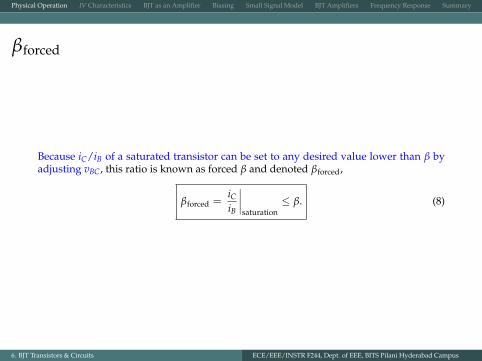
βforced
Because iC/iB of a saturated transistor can be set to any desired value lower than β byadjusting vBC, this ratio is known as forced β and denoted βforced,
βforced =iCiB
∣∣∣∣saturation
≤ β. (8)
6. BJT Transistors & Circuits ECE/EEE/INSTR F244, Dept. of EEE, BITS Pilani Hyderabad Campus
Physical Operation IV Characteristics BJT as an Amplifier Biasing Small Signal Model BJT Amplifiers Frequency Response Summary
βforced
Because iC/iB of a saturated transistor can be set to any desired value lower than β byadjusting vBC, this ratio is known as forced β and denoted βforced,
βforced =iCiB
∣∣∣∣saturation
≤ β. (8)
6. BJT Transistors & Circuits ECE/EEE/INSTR F244, Dept. of EEE, BITS Pilani Hyderabad Campus

Physical Operation IV Characteristics BJT as an Amplifier Biasing Small Signal Model BJT Amplifiers Frequency Response Summary
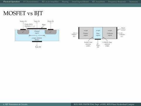
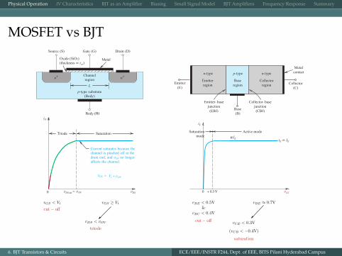
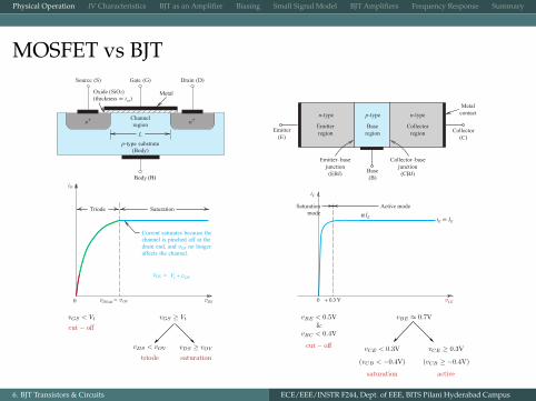
MOSFET vs BJT
6. BJT Transistors & Circuits ECE/EEE/INSTR F244, Dept. of EEE, BITS Pilani Hyderabad Campus
Physical Operation IV Characteristics BJT as an Amplifier Biasing Small Signal Model BJT Amplifiers Frequency Response Summary
MOSFET vs BJT
n+
L
Metal
Channelregion
Oxide (SiO2)(thickness = tox)
p-type substrate(Body)
n+
Source (S) Gate (G) Drain (D)
Bod y (B)
n-type n-type
Emitterregion
Emitter–basejunction(EBJ)
Collector–basejunction(CBJ)
Collector(C)
Emitter(E)
Metalcontact
Collectorregion
p-type
Baseregion
Base(B)
6. BJT Transistors & Circuits ECE/EEE/INSTR F244, Dept. of EEE, BITS Pilani Hyderabad Campus

Physical Operation IV Characteristics BJT as an Amplifier Biasing Small Signal Model BJT Amplifiers Frequency Response Summary
MOSFET vs BJT
n+
L
Metal
Channelregion
Oxide (SiO2)(thickness = tox)
p-type substrate(Body)
n+
Source (S) Gate (G) Drain (D)
Bod y (B)
n-type n-type
Emitterregion
Emitter–basejunction(EBJ)
Collector–basejunction(CBJ)
Collector(C)
Emitter(E)
Metalcontact
Collectorregion
p-type
Baseregion
Base(B)
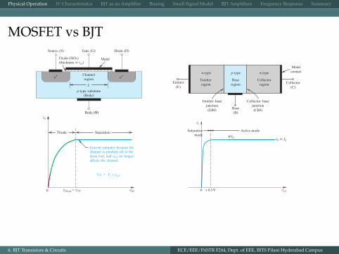
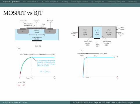
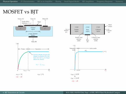
iD
vDS sat =
vGS = +Vt
0
Triode Saturation
vOV
Current saturates because thechannel is pinched off at thedrain end, and vDS no longeraffects the channel.
vDSvOV
6. BJT Transistors & Circuits ECE/EEE/INSTR F244, Dept. of EEE, BITS Pilani Hyderabad Campus
Physical Operation IV Characteristics BJT as an Amplifier Biasing Small Signal Model BJT Amplifiers Frequency Response Summary
MOSFET vs BJT
n+
L
Metal
Channelregion
Oxide (SiO2)(thickness = tox)
p-type substrate(Body)
n+
Source (S) Gate (G) Drain (D)
Bod y (B)
n-type n-type
Emitterregion
Emitter–basejunction(EBJ)
Collector–basejunction(CBJ)
Collector(C)
Emitter(E)
Metalcontact
Collectorregion
p-type
Baseregion
Base(B)
vCE
Saturationmode
Active mode
α IE iE= IE
+ 0.3 V
iC
0
iD
vDS sat =
vGS = +Vt
0
Triode Saturation
vOV
Current saturates because thechannel is pinched off at thedrain end, and vDS no longeraffects the channel.
vDSvOV
6. BJT Transistors & Circuits ECE/EEE/INSTR F244, Dept. of EEE, BITS Pilani Hyderabad Campus

Physical Operation IV Characteristics BJT as an Amplifier Biasing Small Signal Model BJT Amplifiers Frequency Response Summary
pnp BJT
VEB VBC
B
C
vBCvEBiEiE
iE
iCiC
iB
iB
iB1
iB2
iC
Recombinedholes
Injectedelectrons
E
Forward-biased
iE
iC
p n p
Reverse-biased
++ ––
Injected holes Diffusing holes Collected holes
6. BJT Transistors & Circuits ECE/EEE/INSTR F244, Dept. of EEE, BITS Pilani Hyderabad Campus

Physical Operation IV Characteristics BJT as an Amplifier Biasing Small Signal Model BJT Amplifiers Frequency Response Summary
Large-signal Model of pnp BJT
(IS α)
C
E
B
iB
iE
vEB DE
iC
ISevEB VT
+
E
B C
iB
DB
iC
iE
vEB+
ISevEB VT
(IS )β
6. BJT Transistors & Circuits ECE/EEE/INSTR F244, Dept. of EEE, BITS Pilani Hyderabad Campus
Physical Operation IV Characteristics BJT as an Amplifier Biasing Small Signal Model BJT Amplifiers Frequency Response Summary
Outline
1 Physical Operation
2 IV Characteristics
3 BJT as an Amplifier
4 Biasing
5 Small Signal Model
6 BJT Amplifiers
7 Frequency Response
8 Summary
6. BJT Transistors & Circuits ECE/EEE/INSTR F244, Dept. of EEE, BITS Pilani Hyderabad Campus
Physical Operation IV Characteristics BJT as an Amplifier Biasing Small Signal Model BJT Amplifiers Frequency Response Summary
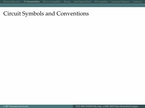
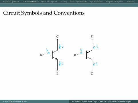
Circuit Symbols and Conventions
B
C
E
B
C
E
iC
iE
iB
iC
iEiB
6. BJT Transistors & Circuits ECE/EEE/INSTR F244, Dept. of EEE, BITS Pilani Hyderabad Campus
Physical Operation IV Characteristics BJT as an Amplifier Biasing Small Signal Model BJT Amplifiers Frequency Response Summary
Circuit Symbols and Conventions
B
C
E
B
C
E
iC
iE
iB
iC
iEiB
6. BJT Transistors & Circuits ECE/EEE/INSTR F244, Dept. of EEE, BITS Pilani Hyderabad Campus

Physical Operation IV Characteristics BJT as an Amplifier Biasing Small Signal Model BJT Amplifiers Frequency Response Summary
iC vs vCB
vCB
iC
Saturationmode
Active mode
α IE iE= IE
Expandedscale
0.4 V 0
6. BJT Transistors & Circuits ECE/EEE/INSTR F244, Dept. of EEE, BITS Pilani Hyderabad Campus
Physical Operation IV Characteristics BJT as an Amplifier Biasing Small Signal Model BJT Amplifiers Frequency Response Summary
iC vs vCB
vCB
iC
Saturationmode
Active mode
α IE iE= IE
Expandedscale
0.4 V 0
6. BJT Transistors & Circuits ECE/EEE/INSTR F244, Dept. of EEE, BITS Pilani Hyderabad Campus
Physical Operation IV Characteristics BJT as an Amplifier Biasing Small Signal Model BJT Amplifiers Frequency Response Summary
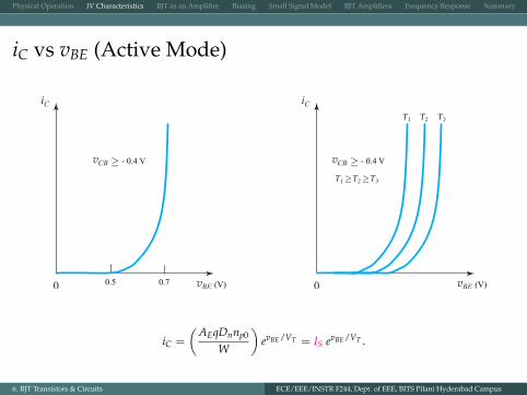
iC vs vBE (Active Mode)
vCB
vBE
iC
0
- 0.4 V
(V)0.5 0.7
vCB
vBE
iC
0
- 0.4 V
(V)
T1 T2 T3
T1 T2 T3
iC =
(AEqDnnp0
W
)evBE/VT = IS evBE/VT .
6. BJT Transistors & Circuits ECE/EEE/INSTR F244, Dept. of EEE, BITS Pilani Hyderabad Campus
Physical Operation IV Characteristics BJT as an Amplifier Biasing Small Signal Model BJT Amplifiers Frequency Response Summary
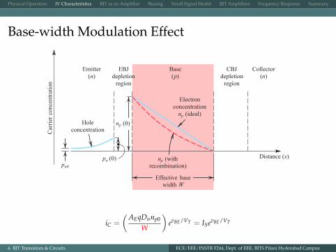
Base-width Modulation Effect
Emitter(n)
EBJdepletion
region
Base(p)
CBJdepletion
region
Collector(n)
Car
rier
con
cent
rati
on
Holeconcentration
Effective basewidth W
Distance (x)
np (0)
Electronconcentrationnp (ideal)
np (withrecombination)
pn (0)pn0
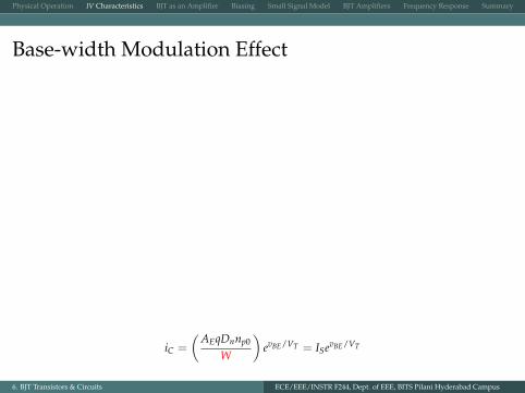
iC =
(AEqDnnp0
W
)evBE/VT = ISevBE/VT
6. BJT Transistors & Circuits ECE/EEE/INSTR F244, Dept. of EEE, BITS Pilani Hyderabad Campus
Physical Operation IV Characteristics BJT as an Amplifier Biasing Small Signal Model BJT Amplifiers Frequency Response Summary
Base-width Modulation Effect
Emitter(n)
EBJdepletion
region
Base(p)
CBJdepletion
region
Collector(n)
Car
rier
con
cent
rati
on
Holeconcentration
Effective basewidth W
Distance (x)
np (0)
Electronconcentrationnp (ideal)
np (withrecombination)
pn (0)pn0
iC =
(AEqDnnp0
W
)evBE/VT = ISevBE/VT
6. BJT Transistors & Circuits ECE/EEE/INSTR F244, Dept. of EEE, BITS Pilani Hyderabad Campus

Physical Operation IV Characteristics BJT as an Amplifier Biasing Small Signal Model BJT Amplifiers Frequency Response Summary
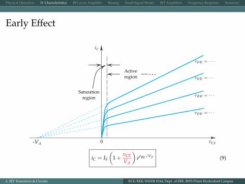
Early Effect
vCE
iC
0
Saturationregion
Activeregion
-VA
iC = IS
(1 +
vCE
VA
)evBE/VT (9)
6. BJT Transistors & Circuits ECE/EEE/INSTR F244, Dept. of EEE, BITS Pilani Hyderabad Campus
Physical Operation IV Characteristics BJT as an Amplifier Biasing Small Signal Model BJT Amplifiers Frequency Response Summary
Early Effect
vCE
iC
0
Saturationregion
Activeregion
-VA
iC = IS
(1 +
vCE
VA
)evBE/VT (9)
6. BJT Transistors & Circuits ECE/EEE/INSTR F244, Dept. of EEE, BITS Pilani Hyderabad Campus

Physical Operation IV Characteristics BJT as an Amplifier Biasing Small Signal Model BJT Amplifiers Frequency Response Summary
Large-signal Models of npn (Including Early Effect)
E
B C
iB
DB
iC
iE
vBE+
(ISB= IS )β
E
B C
iB
DB
iC
iE
vBE+
(ISB= IS )β
ISevBE VT
β iB
6. BJT Transistors & Circuits ECE/EEE/INSTR F244, Dept. of EEE, BITS Pilani Hyderabad Campus
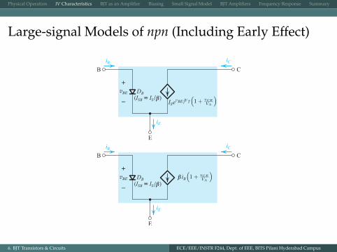
Physical Operation IV Characteristics BJT as an Amplifier Biasing Small Signal Model BJT Amplifiers Frequency Response Summary
Large-signal Models of npn (Including Early Effect)
E
B C
iB
DB
iC
iE
vBE+
(ISB= IS )β
E
B C
iB
DB
iC
iE
vBE+
(ISB= IS )β
ISevBE VT
β iB
6. BJT Transistors & Circuits ECE/EEE/INSTR F244, Dept. of EEE, BITS Pilani Hyderabad Campus
Physical Operation IV Characteristics BJT as an Amplifier Biasing Small Signal Model BJT Amplifiers Frequency Response Summary
Outline
1 Physical Operation
2 IV Characteristics
3 BJT as an Amplifier
4 Biasing
5 Small Signal Model
6 BJT Amplifiers
7 Frequency Response
8 Summary
6. BJT Transistors & Circuits ECE/EEE/INSTR F244, Dept. of EEE, BITS Pilani Hyderabad Campus
Physical Operation IV Characteristics BJT as an Amplifier Biasing Small Signal Model BJT Amplifiers Frequency Response Summary
Stripped Down Version of CE Amplifier & its VTC
6. BJT Transistors & Circuits ECE/EEE/INSTR F244, Dept. of EEE, BITS Pilani Hyderabad Campus
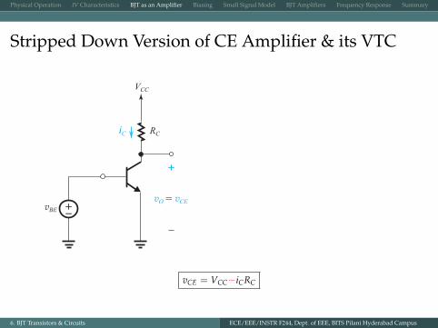
Physical Operation IV Characteristics BJT as an Amplifier Biasing Small Signal Model BJT Amplifiers Frequency Response Summary
Stripped Down Version of CE Amplifier & its VTC
vBEvO= vCE
RC
VCC
iC
+-
+
vCE = VCC−iCRC
6. BJT Transistors & Circuits ECE/EEE/INSTR F244, Dept. of EEE, BITS Pilani Hyderabad Campus
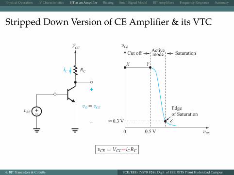
Physical Operation IV Characteristics BJT as an Amplifier Biasing Small Signal Model BJT Amplifiers Frequency Response Summary
Stripped Down Version of CE Amplifier & its VTC
vBEvO= vCE
RC
VCC
0 0.5 V vBE
X Y
Z
iC
0.3 V
Edgeof Saturation
Cut off SaturationActivemode
+-
+
vCE
vCE = VCC−iCRC
6. BJT Transistors & Circuits ECE/EEE/INSTR F244, Dept. of EEE, BITS Pilani Hyderabad Campus
Physical Operation IV Characteristics BJT as an Amplifier Biasing Small Signal Model BJT Amplifiers Frequency Response Summary
Biasing the BJT to Obtain Linear Amplification
VCC
vCE
0 VBE vBE
X Y
VCE
Z
Q
VBEVCE
RC
VCC
IC
+
At point Q (bias / operating / quiescent point),
VCE = VCC − ICRC = VCC − RCISeVBE/VT . (10)
6. BJT Transistors & Circuits ECE/EEE/INSTR F244, Dept. of EEE, BITS Pilani Hyderabad Campus
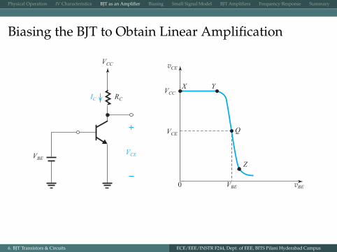
Physical Operation IV Characteristics BJT as an Amplifier Biasing Small Signal Model BJT Amplifiers Frequency Response Summary
Biasing the BJT ... Cont’d
vBE
vce
Q
Z
XSlope= Av
Time
Time
0
vCE
VCC
VCE
vbe
Cutoff SaturationActivemode
0.5
Y
VBE
RC
VCC
vBEvbe
VBE
vCE
iC
+-
+
+
6. BJT Transistors & Circuits ECE/EEE/INSTR F244, Dept. of EEE, BITS Pilani Hyderabad Campus
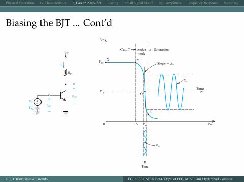
Physical Operation IV Characteristics BJT as an Amplifier Biasing Small Signal Model BJT Amplifiers Frequency Response Summary
The Small-signal Voltage Gain
Since in active region,
vCE = VCC − iCRC = VCC − RCISevBE/VT ,
small-signal voltage gain (i.e., the slope of the tangent to the VTC at Q) is given by
Av =∂vCE
∂vBE
∣∣∣∣vBE=VBE
= −RCISeVBE/VT × 1VT
= − IC
VTRC. (11)
Therefore,
|Av|max ≈VCC
VT. (12)
6. BJT Transistors & Circuits ECE/EEE/INSTR F244, Dept. of EEE, BITS Pilani Hyderabad Campus
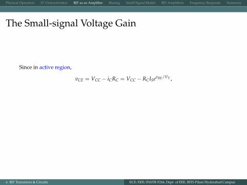
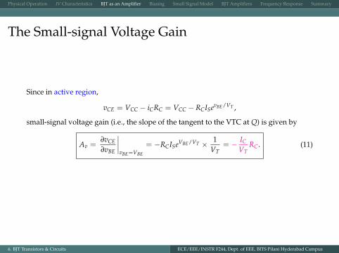
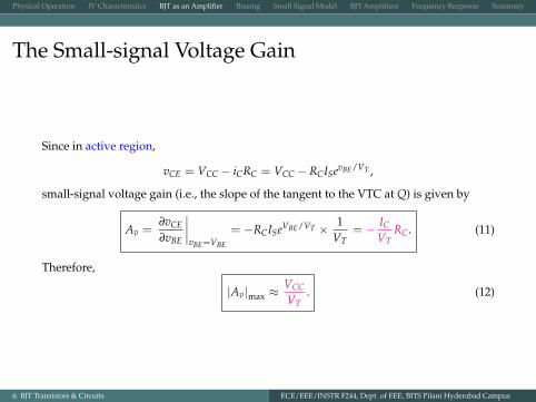

Physical Operation IV Characteristics BJT as an Amplifier Biasing Small Signal Model BJT Amplifiers Frequency Response Summary
Locating the Bias Point Q using VTC
6. BJT Transistors & Circuits ECE/EEE/INSTR F244, Dept. of EEE, BITS Pilani Hyderabad Campus
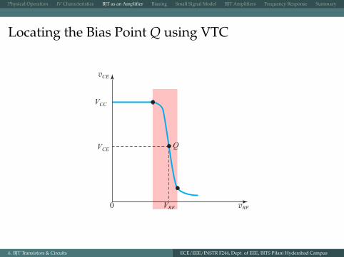
Physical Operation IV Characteristics BJT as an Amplifier Biasing Small Signal Model BJT Amplifiers Frequency Response Summary
Locating the Bias Point Q using VTC
VCC
vCE
0 VBE vBE
VCE Q
6. BJT Transistors & Circuits ECE/EEE/INSTR F244, Dept. of EEE, BITS Pilani Hyderabad Campus

Physical Operation IV Characteristics BJT as an Amplifier Biasing Small Signal Model BJT Amplifiers Frequency Response Summary
Locating the Bias Point Q using VTC ... Cont’d
VCC
vCE
0 VBE vBE
VCE Q
6. BJT Transistors & Circuits ECE/EEE/INSTR F244, Dept. of EEE, BITS Pilani Hyderabad Campus
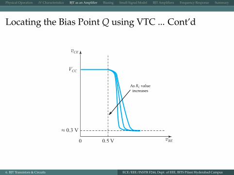
Physical Operation IV Characteristics BJT as an Amplifier Biasing Small Signal Model BJT Amplifiers Frequency Response Summary
Locating the Bias Point Q using VTC ... Cont’d
VCC
vCE
0 vBE
As RC valueincreases
0.5 V
0.3 V
6. BJT Transistors & Circuits ECE/EEE/INSTR F244, Dept. of EEE, BITS Pilani Hyderabad Campus
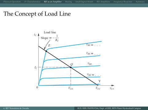
Physical Operation IV Characteristics BJT as an Amplifier Biasing Small Signal Model BJT Amplifiers Frequency Response Summary
The Concept of Load Line
= . . .
iC
IC
V
Z
Y
CE VCC vCE
Load line
Slope =1RC
Q
0
vBE
= . . .vBE
= . . .vBE
vBE
6. BJT Transistors & Circuits ECE/EEE/INSTR F244, Dept. of EEE, BITS Pilani Hyderabad Campus
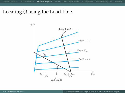
Physical Operation IV Characteristics BJT as an Amplifier Biasing Small Signal Model BJT Amplifiers Frequency Response Summary
Locating Q using the Load Line
iC
vCE
Load-line A
QB
QA
VCEQB
VCE VCC
Load-line B
QA
= . . .vBE
= . . .vBE
=vBE VBE
6. BJT Transistors & Circuits ECE/EEE/INSTR F244, Dept. of EEE, BITS Pilani Hyderabad Campus
Physical Operation IV Characteristics BJT as an Amplifier Biasing Small Signal Model BJT Amplifiers Frequency Response Summary
Outline
1 Physical Operation
2 IV Characteristics
3 BJT as an Amplifier
4 Biasing
5 Small Signal Model
6 BJT Amplifiers
7 Frequency Response
8 Summary
6. BJT Transistors & Circuits ECE/EEE/INSTR F244, Dept. of EEE, BITS Pilani Hyderabad Campus

Physical Operation IV Characteristics BJT as an Amplifier Biasing Small Signal Model BJT Amplifiers Frequency Response Summary
Biasing & Bias Stabilization
We need biasing for choosing an appropriate operating point.
Bias stabilization is necessary to obtain same gain irrespective of variation inparameters such as β, T, etc.
Bias stabilization can be achieved by maintaining constant IC, similar to thecase of MOSFET where we tried to maintain constant ID.
6. BJT Transistors & Circuits ECE/EEE/INSTR F244, Dept. of EEE, BITS Pilani Hyderabad Campus
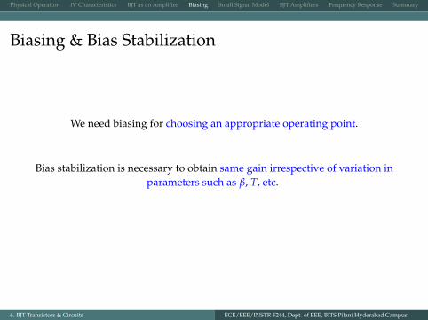
Physical Operation IV Characteristics BJT as an Amplifier Biasing Small Signal Model BJT Amplifiers Frequency Response Summary
Biasing & Bias Stabilization
We need biasing for choosing an appropriate operating point.
Bias stabilization is necessary to obtain same gain irrespective of variation inparameters such as β, T, etc.
Bias stabilization can be achieved by maintaining constant IC, similar to thecase of MOSFET where we tried to maintain constant ID.
6. BJT Transistors & Circuits ECE/EEE/INSTR F244, Dept. of EEE, BITS Pilani Hyderabad Campus
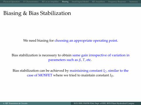
Physical Operation IV Characteristics BJT as an Amplifier Biasing Small Signal Model BJT Amplifiers Frequency Response Summary
Biasing & Bias Stabilization
We need biasing for choosing an appropriate operating point.
Bias stabilization is necessary to obtain same gain irrespective of variation inparameters such as β, T, etc.
Bias stabilization can be achieved by maintaining constant IC, similar to thecase of MOSFET where we tried to maintain constant ID.
6. BJT Transistors & Circuits ECE/EEE/INSTR F244, Dept. of EEE, BITS Pilani Hyderabad Campus

Physical Operation IV Characteristics BJT as an Amplifier Biasing Small Signal Model BJT Amplifiers Frequency Response Summary
1. Biasing by Fixing VBE (Bad)
RB2
RB1
VBE
RC
VCC
IC
IBVCE
RB RC
VCC
IC
IB
VCE
VBE
+ +
6. BJT Transistors & Circuits ECE/EEE/INSTR F244, Dept. of EEE, BITS Pilani Hyderabad Campus
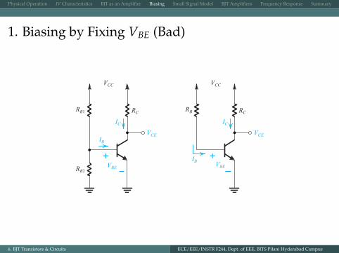
Physical Operation IV Characteristics BJT as an Amplifier Biasing Small Signal Model BJT Amplifiers Frequency Response Summary
1. Biasing by Fixing VBE (Bad)
RB2
RB1
VBE
RC
VCC
IC
IBVCE
RB RC
VCC
IC
IB
VCE
VBE
+ +
6. BJT Transistors & Circuits ECE/EEE/INSTR F244, Dept. of EEE, BITS Pilani Hyderabad Campus
Physical Operation IV Characteristics BJT as an Amplifier Biasing Small Signal Model BJT Amplifiers Frequency Response Summary
1. Biasing by Fixing VBE (Bad)
iC
vBEVBE
IC1
0
IC2
Device 2
Device 1
6. BJT Transistors & Circuits ECE/EEE/INSTR F244, Dept. of EEE, BITS Pilani Hyderabad Campus
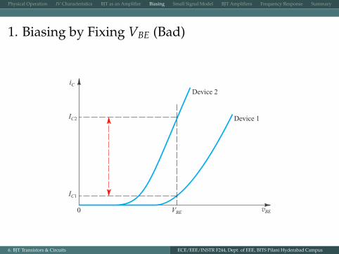
Physical Operation IV Characteristics BJT as an Amplifier Biasing Small Signal Model BJT Amplifiers Frequency Response Summary
1. Biasing by Fixing VBE (Bad)
iC
vBEVBE
IC1
0
IC2
Device 2
Device 1
6. BJT Transistors & Circuits ECE/EEE/INSTR F244, Dept. of EEE, BITS Pilani Hyderabad Campus

Physical Operation IV Characteristics BJT as an Amplifier Biasing Small Signal Model BJT Amplifiers Frequency Response Summary
2. The Classical Discrete-Circuit Bias Arrangement
R1
RER2
VCC
RC
VBB VCCR1 R2
R2
RB R1 R2
IB
IE
IC
=
RC
RE
VCC
=
+
VBB = IBRB + VBE + IERE
⇒ IE =VBB −VBE
RE + RB1+β
.
So, to make IE insensitive to temperatureand β variation,
VBB � VBE
RE � RB
β + 1
6. BJT Transistors & Circuits ECE/EEE/INSTR F244, Dept. of EEE, BITS Pilani Hyderabad Campus
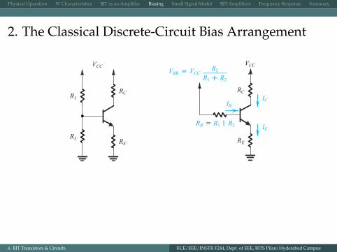
Physical Operation IV Characteristics BJT as an Amplifier Biasing Small Signal Model BJT Amplifiers Frequency Response Summary
2. The Classical Discrete-Circuit Bias Arrangement
R1
RER2
VCC
RC
VBB VCCR1 R2
R2
RB R1 R2
IB
IE
IC
=
RC
RE
VCC
=
+
VBB = IBRB + VBE + IERE
⇒ IE =VBB −VBE
RE + RB1+β
.
So, to make IE insensitive to temperatureand β variation,
VBB � VBE
RE � RB
β + 1
6. BJT Transistors & Circuits ECE/EEE/INSTR F244, Dept. of EEE, BITS Pilani Hyderabad Campus
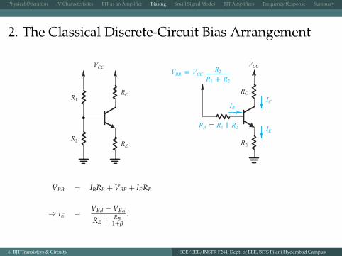
Physical Operation IV Characteristics BJT as an Amplifier Biasing Small Signal Model BJT Amplifiers Frequency Response Summary
2. The Classical Discrete-Circuit Bias Arrangement
R1
RER2
VCC
RC
VBB VCCR1 R2
R2
RB R1 R2
IB
IE
IC
=
RC
RE
VCC
=
+
VBB = IBRB + VBE + IERE
⇒ IE =VBB −VBE
RE + RB1+β
.
So, to make IE insensitive to temperatureand β variation,
VBB � VBE
RE � RB
β + 1
6. BJT Transistors & Circuits ECE/EEE/INSTR F244, Dept. of EEE, BITS Pilani Hyderabad Campus
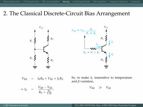
Physical Operation IV Characteristics BJT as an Amplifier Biasing Small Signal Model BJT Amplifiers Frequency Response Summary
2. The Classical Discrete-Circuit Bias Arrangement
R1
RER2
VCC
RC
VBB VCCR1 R2
R2
RB R1 R2
IB
IE
IC
=
RC
RE
VCC
=
+
VBB = IBRB + VBE + IERE
⇒ IE =VBB −VBE
RE + RB1+β
.
So, to make IE insensitive to temperatureand β variation,
VBB � VBE
RE � RB
β + 1
6. BJT Transistors & Circuits ECE/EEE/INSTR F244, Dept. of EEE, BITS Pilani Hyderabad Campus

Physical Operation IV Characteristics BJT as an Amplifier Biasing Small Signal Model BJT Amplifiers Frequency Response Summary
2. A Two-Power-Supply Version of the Classical BiasArrangement
RE
RB
+VCC
RC
-VEE
IB
IE
6. BJT Transistors & Circuits ECE/EEE/INSTR F244, Dept. of EEE, BITS Pilani Hyderabad Campus

Physical Operation IV Characteristics BJT as an Amplifier Biasing Small Signal Model BJT Amplifiers Frequency Response Summary
3. Biasing Using a Collector-to-Base Feedback Resistor
IB
IE
IC
RC
VCC
RB
IE
VCC = IBRB + VBE + IERC
⇒ IE =VCC −VBE
RC + RB1+β
So, to make IE insensitive to temperatureand β variation,
VBB � VBE
RE � RB
β + 1
6. BJT Transistors & Circuits ECE/EEE/INSTR F244, Dept. of EEE, BITS Pilani Hyderabad Campus
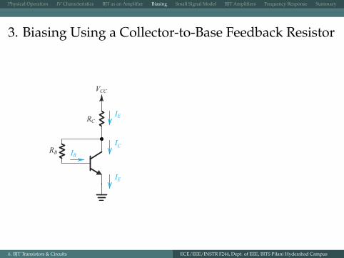
Physical Operation IV Characteristics BJT as an Amplifier Biasing Small Signal Model BJT Amplifiers Frequency Response Summary
3. Biasing Using a Collector-to-Base Feedback Resistor
IB
IE
IC
RC
VCC
RB
IE
VCC = IBRB + VBE + IERC
⇒ IE =VCC −VBE
RC + RB1+β
So, to make IE insensitive to temperatureand β variation,
VBB � VBE
RE � RB
β + 1
6. BJT Transistors & Circuits ECE/EEE/INSTR F244, Dept. of EEE, BITS Pilani Hyderabad Campus
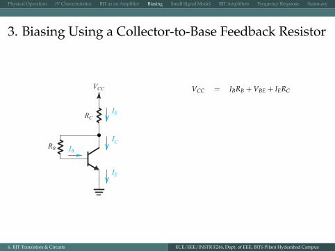
Physical Operation IV Characteristics BJT as an Amplifier Biasing Small Signal Model BJT Amplifiers Frequency Response Summary
3. Biasing Using a Collector-to-Base Feedback Resistor
IB
IE
IC
RC
VCC
RB
IE
VCC = IBRB + VBE + IERC
⇒ IE =VCC −VBE
RC + RB1+β
So, to make IE insensitive to temperatureand β variation,
VBB � VBE
RE � RB
β + 1
6. BJT Transistors & Circuits ECE/EEE/INSTR F244, Dept. of EEE, BITS Pilani Hyderabad Campus
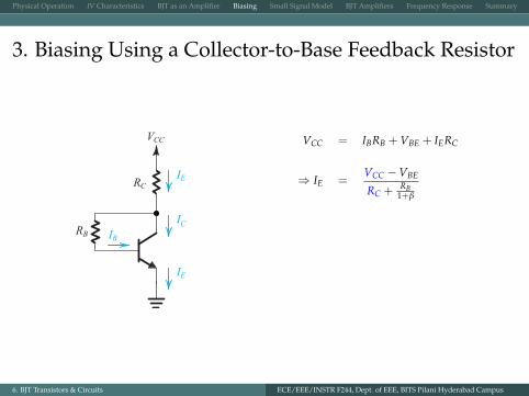
Physical Operation IV Characteristics BJT as an Amplifier Biasing Small Signal Model BJT Amplifiers Frequency Response Summary
3. Biasing Using a Collector-to-Base Feedback Resistor
IB
IE
IC
RC
VCC
RB
IE
VCC = IBRB + VBE + IERC
⇒ IE =VCC −VBE
RC + RB1+β
So, to make IE insensitive to temperatureand β variation,
VBB � VBE
RE � RB
β + 1
6. BJT Transistors & Circuits ECE/EEE/INSTR F244, Dept. of EEE, BITS Pilani Hyderabad Campus
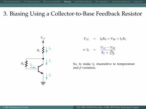
Physical Operation IV Characteristics BJT as an Amplifier Biasing Small Signal Model BJT Amplifiers Frequency Response Summary
3. Biasing Using a Collector-to-Base Feedback Resistor
IB
IE
IC
RC
VCC
RB
IE
VCC = IBRB + VBE + IERC
⇒ IE =VCC −VBE
RC + RB1+β
So, to make IE insensitive to temperatureand β variation,
VBB � VBE
RE � RB
β + 1
6. BJT Transistors & Circuits ECE/EEE/INSTR F244, Dept. of EEE, BITS Pilani Hyderabad Campus
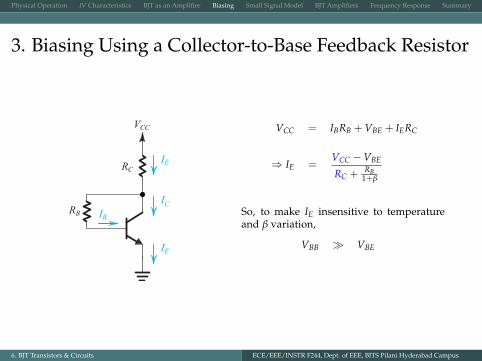
Physical Operation IV Characteristics BJT as an Amplifier Biasing Small Signal Model BJT Amplifiers Frequency Response Summary
3. Biasing Using a Collector-to-Base Feedback Resistor
IB
IE
IC
RC
VCC
RB
IE
VCC = IBRB + VBE + IERC
⇒ IE =VCC −VBE
RC + RB1+β
So, to make IE insensitive to temperatureand β variation,
VBB � VBE
RE � RB
β + 1
6. BJT Transistors & Circuits ECE/EEE/INSTR F244, Dept. of EEE, BITS Pilani Hyderabad Campus
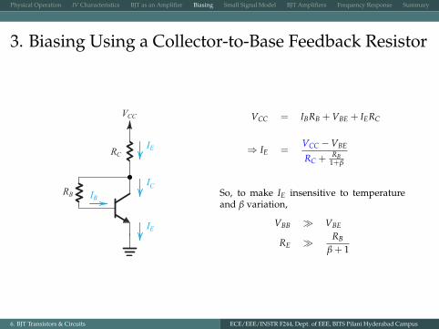
Physical Operation IV Characteristics BJT as an Amplifier Biasing Small Signal Model BJT Amplifiers Frequency Response Summary
3. Biasing Using a Collector-to-Base Feedback Resistor
IB
IE
IC
RC
VCC
RB
IE
VCC = IBRB + VBE + IERC
⇒ IE =VCC −VBE
RC + RB1+β
So, to make IE insensitive to temperatureand β variation,
VBB � VBE
RE � RB
β + 1
6. BJT Transistors & Circuits ECE/EEE/INSTR F244, Dept. of EEE, BITS Pilani Hyderabad Campus
Physical Operation IV Characteristics BJT as an Amplifier Biasing Small Signal Model BJT Amplifiers Frequency Response Summary
4. Biasing Using a Constant-Current Source
6. BJT Transistors & Circuits ECE/EEE/INSTR F244, Dept. of EEE, BITS Pilani Hyderabad Campus
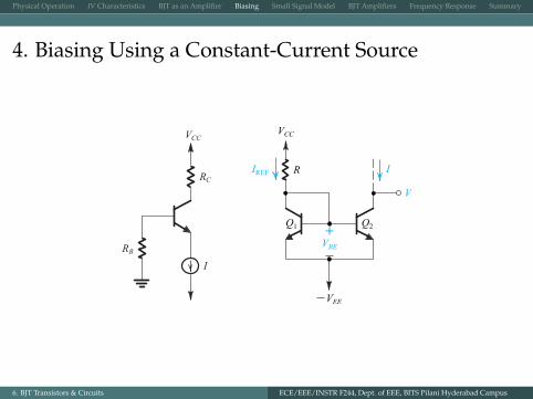
Physical Operation IV Characteristics BJT as an Amplifier Biasing Small Signal Model BJT Amplifiers Frequency Response Summary
4. Biasing Using a Constant-Current Source
6. BJT Transistors & Circuits ECE/EEE/INSTR F244, Dept. of EEE, BITS Pilani Hyderabad Campus

Physical Operation IV Characteristics BJT as an Amplifier Biasing Small Signal Model BJT Amplifiers Frequency Response Summary
Outline
1 Physical Operation
2 IV Characteristics
3 BJT as an Amplifier
4 Biasing
5 Small Signal Model
6 BJT Amplifiers
7 Frequency Response
8 Summary
6. BJT Transistors & Circuits ECE/EEE/INSTR F244, Dept. of EEE, BITS Pilani Hyderabad Campus

Physical Operation IV Characteristics BJT as an Amplifier Biasing Small Signal Model BJT Amplifiers Frequency Response Summary
The Input Resistance at the Base (rπ)
vberπ =
ib
ib
+
vbe
Since iB = ISβ evBE/VT ,
rπ =∂vBE
∂iB
∣∣∣∣vBE=VBE
=
[1
VT
IS
βeVBE/VT
]−1
=VT
IB. (13)
.
6. BJT Transistors & Circuits ECE/EEE/INSTR F244, Dept. of EEE, BITS Pilani Hyderabad Campus
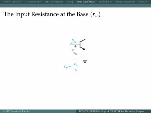
Physical Operation IV Characteristics BJT as an Amplifier Biasing Small Signal Model BJT Amplifiers Frequency Response Summary
The Input Resistance at the Base (rπ)
vberπ =
ib
ib
+
vbe
Since iB = ISβ evBE/VT ,
rπ =∂vBE
∂iB
∣∣∣∣vBE=VBE
=
[1
VT
IS
βeVBE/VT
]−1
=VT
IB. (13)
.
6. BJT Transistors & Circuits ECE/EEE/INSTR F244, Dept. of EEE, BITS Pilani Hyderabad Campus
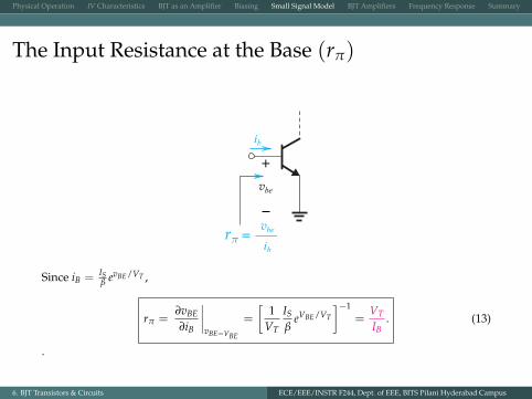
Physical Operation IV Characteristics BJT as an Amplifier Biasing Small Signal Model BJT Amplifiers Frequency Response Summary
The Input Resistance at the Base (rπ)
vberπ =
ib
ib
+
vbe
Since iB = ISβ evBE/VT ,
rπ =∂vBE
∂iB
∣∣∣∣vBE=VBE
=
[1
VT
IS
βeVBE/VT
]−1
=VT
IB. (13)
.
6. BJT Transistors & Circuits ECE/EEE/INSTR F244, Dept. of EEE, BITS Pilani Hyderabad Campus

Physical Operation IV Characteristics BJT as an Amplifier Biasing Small Signal Model BJT Amplifiers Frequency Response Summary
Transconductance (gm)
ic
+
vbe
vBE
iC
0
vCB - 0.4 V
(V)0.5 0.7
Q
Slope = gm
Since iC = ISevBE/VT ,
gm =∂iC
∂vBE
∣∣∣∣vBE=VBE
=1
VTISeVBE/VT =
IC
VT. (14)
6. BJT Transistors & Circuits ECE/EEE/INSTR F244, Dept. of EEE, BITS Pilani Hyderabad Campus
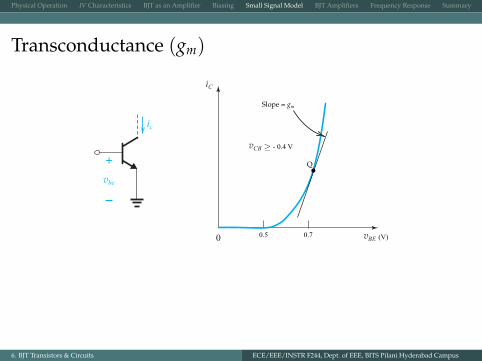
Physical Operation IV Characteristics BJT as an Amplifier Biasing Small Signal Model BJT Amplifiers Frequency Response Summary
Transconductance (gm)
ic
+
vbe
vBE
iC
0
vCB - 0.4 V
(V)0.5 0.7
Q
Slope = gm
Since iC = ISevBE/VT ,
gm =∂iC
∂vBE
∣∣∣∣vBE=VBE
=1
VTISeVBE/VT =
IC
VT. (14)
6. BJT Transistors & Circuits ECE/EEE/INSTR F244, Dept. of EEE, BITS Pilani Hyderabad Campus
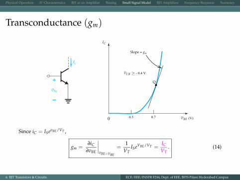
Physical Operation IV Characteristics BJT as an Amplifier Biasing Small Signal Model BJT Amplifiers Frequency Response Summary
Transconductance (gm)
ic
+
vbe
vBE
iC
0
vCB - 0.4 V
(V)0.5 0.7
Q
Slope = gm
Since iC = ISevBE/VT ,
gm =∂iC
∂vBE
∣∣∣∣vBE=VBE
=1
VTISeVBE/VT =
IC
VT. (14)
6. BJT Transistors & Circuits ECE/EEE/INSTR F244, Dept. of EEE, BITS Pilani Hyderabad Campus

Physical Operation IV Characteristics BJT as an Amplifier Biasing Small Signal Model BJT Amplifiers Frequency Response Summary
Small Signal (π) Model of BJT
E
B C+
–
ib ic
ie
vbegmvbe
rπ
E
B C+
–
ib ic
ie
vbe rπ β iB
E
B C+
–
ib ic
ie
vbe rπ αiE
gmvbe =IC
VT× ibrπ =
IC
VT× ib
VT
IB= βib = αie
6. BJT Transistors & Circuits ECE/EEE/INSTR F244, Dept. of EEE, BITS Pilani Hyderabad Campus
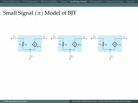
Physical Operation IV Characteristics BJT as an Amplifier Biasing Small Signal Model BJT Amplifiers Frequency Response Summary
Small Signal (π) Model of BJT
E
B C+
–
ib ic
ie
vbegmvbe
rπ
E
B C+
–
ib ic
ie
vbe rπ β iB
E
B C+
–
ib ic
ie
vbe rπ αiE
gmvbe =IC
VT× ibrπ =
IC
VT× ib
VT
IB= βib = αie
6. BJT Transistors & Circuits ECE/EEE/INSTR F244, Dept. of EEE, BITS Pilani Hyderabad Campus

Physical Operation IV Characteristics BJT as an Amplifier Biasing Small Signal Model BJT Amplifiers Frequency Response Summary
Small Signal (π) Model of BJT
E
B C+
–
ib ic
ie
vbegmvbe
rπ
E
B C+
–
ib ic
ie
vbe rπ β iB
E
B C+
–
ib ic
ie
vbe rπ αiE
gmvbe =
IC
VT× ibrπ =
IC
VT× ib
VT
IB= βib = αie
6. BJT Transistors & Circuits ECE/EEE/INSTR F244, Dept. of EEE, BITS Pilani Hyderabad Campus

Physical Operation IV Characteristics BJT as an Amplifier Biasing Small Signal Model BJT Amplifiers Frequency Response Summary
Small Signal (π) Model of BJT
E
B C+
–
ib ic
ie
vbegmvbe
rπ
E
B C+
–
ib ic
ie
vbe rπ β iB
E
B C+
–
ib ic
ie
vbe rπ αiE
gmvbe =IC
VT× ibrπ
=IC
VT× ib
VT
IB= βib = αie
6. BJT Transistors & Circuits ECE/EEE/INSTR F244, Dept. of EEE, BITS Pilani Hyderabad Campus

Physical Operation IV Characteristics BJT as an Amplifier Biasing Small Signal Model BJT Amplifiers Frequency Response Summary
Small Signal (π) Model of BJT
E
B C+
–
ib ic
ie
vbegmvbe
rπ
E
B C+
–
ib ic
ie
vbe rπ β iB
E
B C+
–
ib ic
ie
vbe rπ αiE
gmvbe =IC
VT× ibrπ =
IC
VT× ib
VT
IB
= βib = αie
6. BJT Transistors & Circuits ECE/EEE/INSTR F244, Dept. of EEE, BITS Pilani Hyderabad Campus
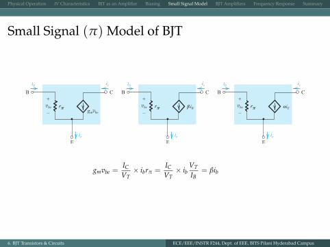
Physical Operation IV Characteristics BJT as an Amplifier Biasing Small Signal Model BJT Amplifiers Frequency Response Summary
Small Signal (π) Model of BJT
E
B C+
–
ib ic
ie
vbegmvbe
rπ
E
B C+
–
ib ic
ie
vbe rπ β iB
E
B C+
–
ib ic
ie
vbe rπ αiE
gmvbe =IC
VT× ibrπ =
IC
VT× ib
VT
IB= βib
= αie
6. BJT Transistors & Circuits ECE/EEE/INSTR F244, Dept. of EEE, BITS Pilani Hyderabad Campus

Physical Operation IV Characteristics BJT as an Amplifier Biasing Small Signal Model BJT Amplifiers Frequency Response Summary
Small Signal (π) Model of BJT
E
B C+
–
ib ic
ie
vbegmvbe
rπ
E
B C+
–
ib ic
ie
vbe rπ β iB
E
B C+
–
ib ic
ie
vbe rπ αiE
gmvbe =IC
VT× ibrπ =
IC
VT× ib
VT
IB= βib = αie
6. BJT Transistors & Circuits ECE/EEE/INSTR F244, Dept. of EEE, BITS Pilani Hyderabad Campus
Physical Operation IV Characteristics BJT as an Amplifier Biasing Small Signal Model BJT Amplifiers Frequency Response Summary
Small Signal (T) Model of BJT
E
B C+
–
ib ic
ie
vbegmvbe
rπ
C
B
E
ic
ib
re
ie
gmvbe
+
–
vbe
�� ��If both the above circuits are equivalent, then what should be the value of re?
6. BJT Transistors & Circuits ECE/EEE/INSTR F244, Dept. of EEE, BITS Pilani Hyderabad Campus
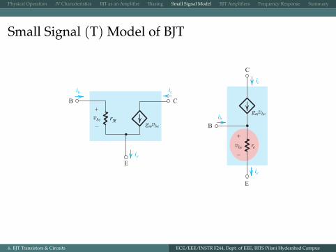
Physical Operation IV Characteristics BJT as an Amplifier Biasing Small Signal Model BJT Amplifiers Frequency Response Summary
Small Signal T Model of BJT ... Cont’d
E
B C+
–
ib ic
ie
vbegmvbe
rπ
C
B
E
ic
ib
re
ie
gmvbe
+
–
vbe
Voltage drop across rπ and re is same and equal to vbe. Therefore,
reie = rπ ib ⇒ re = rπibie
=rπ
1 + β. (15)
6. BJT Transistors & Circuits ECE/EEE/INSTR F244, Dept. of EEE, BITS Pilani Hyderabad Campus
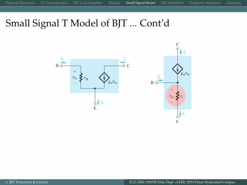
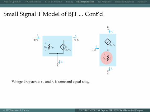
Physical Operation IV Characteristics BJT as an Amplifier Biasing Small Signal Model BJT Amplifiers Frequency Response Summary
Small Signal T Model of BJT ... Cont’d
E
B C+
–
ib ic
ie
vbegmvbe
rπ
C
B
E
ic
ib
re
ie
gmvbe
+
–
vbe
Voltage drop across rπ and re is same and equal to vbe.
Therefore,
reie = rπ ib ⇒ re = rπibie
=rπ
1 + β. (15)
6. BJT Transistors & Circuits ECE/EEE/INSTR F244, Dept. of EEE, BITS Pilani Hyderabad Campus
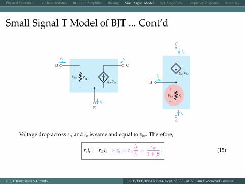
Physical Operation IV Characteristics BJT as an Amplifier Biasing Small Signal Model BJT Amplifiers Frequency Response Summary
Small Signal T Model of BJT ... Cont’d
E
B C+
–
ib ic
ie
vbegmvbe
rπ
C
B
E
ic
ib
re
ie
gmvbe
+
–
vbe
Voltage drop across rπ and re is same and equal to vbe. Therefore,
reie = rπ ib ⇒ re = rπibie
=rπ
1 + β. (15)
6. BJT Transistors & Circuits ECE/EEE/INSTR F244, Dept. of EEE, BITS Pilani Hyderabad Campus
Physical Operation IV Characteristics BJT as an Amplifier Biasing Small Signal Model BJT Amplifiers Frequency Response Summary
Small Signal Model (Including Early Effect)
vCE
iC
0
Saturationregion
Activeregion
-VA
iC = IS
(1 +
vCE
VA
)evBE/VT (16)
6. BJT Transistors & Circuits ECE/EEE/INSTR F244, Dept. of EEE, BITS Pilani Hyderabad Campus
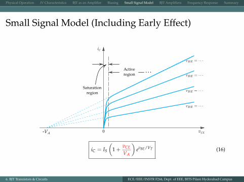

Physical Operation IV Characteristics BJT as an Amplifier Biasing Small Signal Model BJT Amplifiers Frequency Response Summary
Small Signal Model (Including Early Effect) ... Cont’d
gm = IC /VTrπ = IBVT/
E
B C+
–
ib ic
ie
vbegmvbe
rπ ro
E
B C+
–
ib ic
ie
vbe rπ roβ iB
From (16),
ro =
(∂iC
∂vCE
∣∣∣∣vBE=constant
)−1
=
(IS
VAeVBE/VT
)−1
=VA
ISeVBE/VT=
VA
I′C, (17)
where I′C is the value of the collector current with the Early effect neglected.
6. BJT Transistors & Circuits ECE/EEE/INSTR F244, Dept. of EEE, BITS Pilani Hyderabad Campus
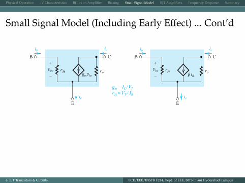
Physical Operation IV Characteristics BJT as an Amplifier Biasing Small Signal Model BJT Amplifiers Frequency Response Summary
Small Signal Model (Including Early Effect) ... Cont’d
gm = IC /VTrπ = IBVT/
E
B C+
–
ib ic
ie
vbegmvbe
rπ ro
E
B C+
–
ib ic
ie
vbe rπ roβ iB
From (16),
ro =
(∂iC
∂vCE
∣∣∣∣vBE=constant
)−1
=
(IS
VAeVBE/VT
)−1
=VA
ISeVBE/VT=
VA
I′C, (17)
where I′C is the value of the collector current with the Early effect neglected.
6. BJT Transistors & Circuits ECE/EEE/INSTR F244, Dept. of EEE, BITS Pilani Hyderabad Campus
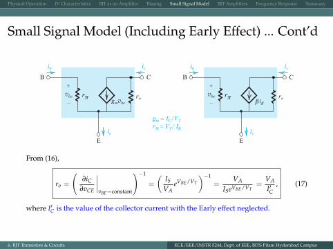
Physical Operation IV Characteristics BJT as an Amplifier Biasing Small Signal Model BJT Amplifiers Frequency Response Summary
Small Signal Model (Including Early Effect) ... Cont’d
gm = IC /VTrπ = IBVT/
E
B C+
–
ib ic
ie
vbegmvbe
rπ ro
E
B C+
–
ib ic
ie
vbe rπ roβ iB
From (16),
ro =
(∂iC
∂vCE
∣∣∣∣vBE=constant
)−1
=
(IS
VAeVBE/VT
)−1
=VA
ISeVBE/VT=
VA
I′C, (17)
where I′C is the value of the collector current with the Early effect neglected.
6. BJT Transistors & Circuits ECE/EEE/INSTR F244, Dept. of EEE, BITS Pilani Hyderabad Campus

Physical Operation IV Characteristics BJT as an Amplifier Biasing Small Signal Model BJT Amplifiers Frequency Response Summary
Outline
1 Physical Operation
2 IV Characteristics
3 BJT as an Amplifier
4 Biasing
5 Small Signal Model
6 BJT Amplifiers
7 Frequency Response
8 Summary
6. BJT Transistors & Circuits ECE/EEE/INSTR F244, Dept. of EEE, BITS Pilani Hyderabad Campus

Physical Operation IV Characteristics BJT as an Amplifier Biasing Small Signal Model BJT Amplifiers Frequency Response Summary
BJT is Basically a Current Amplifier!
gm = IC /VTrπ = IBVT/
E
B C+
–
ib ic
ie
vbegmvbe
rπ ro
E
B C+
–
ib ic
ie
vbe rπ roβ iB
rπ ≈ 0 and ro → ∞
6. BJT Transistors & Circuits ECE/EEE/INSTR F244, Dept. of EEE, BITS Pilani Hyderabad Campus
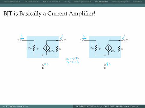
Physical Operation IV Characteristics BJT as an Amplifier Biasing Small Signal Model BJT Amplifiers Frequency Response Summary
BJT is Basically a Current Amplifier!
gm = IC /VTrπ = IBVT/
E
B C+
–
ib ic
ie
vbegmvbe
rπ ro
E
B C+
–
ib ic
ie
vbe rπ roβ iB
rπ ≈ 0 and ro → ∞
6. BJT Transistors & Circuits ECE/EEE/INSTR F244, Dept. of EEE, BITS Pilani Hyderabad Campus
Physical Operation IV Characteristics BJT as an Amplifier Biasing Small Signal Model BJT Amplifiers Frequency Response Summary
Basic Configurations (Stripped Down Versions)
vi
RL
(c) Common-Collector (CC)or Emitter Follower
vo
_+
vi
RC
(a) Common-Emitter (CE)
vo
_+ vi
RC
(b) Common-Base (CB)
vo
_+
6. BJT Transistors & Circuits ECE/EEE/INSTR F244, Dept. of EEE, BITS Pilani Hyderabad Campus
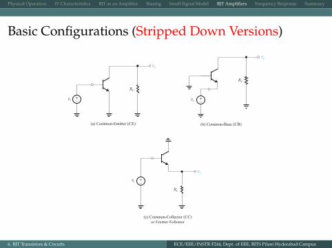
Physical Operation IV Characteristics BJT as an Amplifier Biasing Small Signal Model BJT Amplifiers Frequency Response Summary
Various Definitions of Gain – Recap
+vi
+
vo
+
R0
RiAvovi+vs RL
RSii io
Avo =vo
vI
∣∣∣∣RL→∞
Av = AvoRL
RL + Ro
Gv =vo
vs= Avo
(Ri
Ri + RS
)(RL
RL + Ro
)
6. BJT Transistors & Circuits ECE/EEE/INSTR F244, Dept. of EEE, BITS Pilani Hyderabad Campus
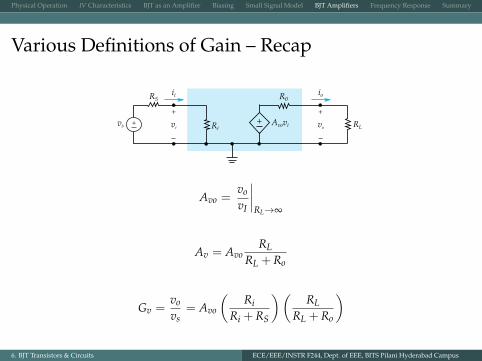
Physical Operation IV Characteristics BJT as an Amplifier Biasing Small Signal Model BJT Amplifiers Frequency Response Summary
First Let’s Analyze Simple CS Amplifier ...
6. BJT Transistors & Circuits ECE/EEE/INSTR F244, Dept. of EEE, BITS Pilani Hyderabad Campus
Physical Operation IV Characteristics BJT as an Amplifier Biasing Small Signal Model BJT Amplifiers Frequency Response Summary
1. CE Amplifier
6. BJT Transistors & Circuits ECE/EEE/INSTR F244, Dept. of EEE, BITS Pilani Hyderabad Campus
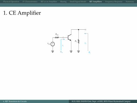
Physical Operation IV Characteristics BJT as an Amplifier Biasing Small Signal Model BJT Amplifiers Frequency Response Summary
1. CE Amplifier
vi
Rin Ro
voRC
vsig
Rsig
_+
6. BJT Transistors & Circuits ECE/EEE/INSTR F244, Dept. of EEE, BITS Pilani Hyderabad Campus

Physical Operation IV Characteristics BJT as an Amplifier Biasing Small Signal Model BJT Amplifiers Frequency Response Summary
1. CE Amplifier
vi
Rin Ro
voRC
vsig
Rsig
v = vi
Rin=
vsig
Rsig
vo
Ro= RC||ro
gmvbeRCro
_+
_+ rπ
rπ
Avo = −gm (ro ‖ RC) Av = −gm (ro ‖ RC ‖ RL) Gv = Av × rπRsig+rπ
6. BJT Transistors & Circuits ECE/EEE/INSTR F244, Dept. of EEE, BITS Pilani Hyderabad Campus
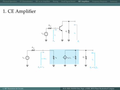
Physical Operation IV Characteristics BJT as an Amplifier Biasing Small Signal Model BJT Amplifiers Frequency Response Summary
1. CE Amplifier
vi
Rin Ro
voRC
vsig
Rsig
v = vi
Rin=
vsig
Rsig
vo
Ro= RC||ro
gmvbeRCro
_+
_+ rπ
rπ
Avo = −gm (ro ‖ RC)
Av = −gm (ro ‖ RC ‖ RL) Gv = Av × rπRsig+rπ
6. BJT Transistors & Circuits ECE/EEE/INSTR F244, Dept. of EEE, BITS Pilani Hyderabad Campus
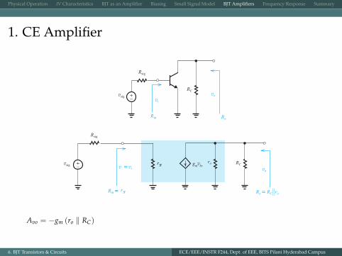
Physical Operation IV Characteristics BJT as an Amplifier Biasing Small Signal Model BJT Amplifiers Frequency Response Summary
1. CE Amplifier
vi
Rin Ro
voRC
vsig
Rsig
v = vi
Rin=
vsig
Rsig
vo
Ro= RC||ro
gmvbeRCro
_+
_+ rπ
rπ
Avo = −gm (ro ‖ RC)
Av = −gm (ro ‖ RC ‖ RL) Gv = Av × rπRsig+rπ
6. BJT Transistors & Circuits ECE/EEE/INSTR F244, Dept. of EEE, BITS Pilani Hyderabad Campus

Physical Operation IV Characteristics BJT as an Amplifier Biasing Small Signal Model BJT Amplifiers Frequency Response Summary
1. CE Amplifier
vi
Rin Ro
voRC
vsig
Rsig
v = vi
Rin=
vsig
Rsig
vo
Ro= RC||ro
gmvbeRCro
_+
_+ rπ
rπ
Avo = −gm (ro ‖ RC) Av = −gm (ro ‖ RC ‖ RL)
Gv = Av × rπRsig+rπ
6. BJT Transistors & Circuits ECE/EEE/INSTR F244, Dept. of EEE, BITS Pilani Hyderabad Campus
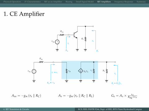
Physical Operation IV Characteristics BJT as an Amplifier Biasing Small Signal Model BJT Amplifiers Frequency Response Summary
1. CE Amplifier
vi
Rin Ro
voRC
vsig
Rsig
v = vi
Rin=
vsig
Rsig
vo
Ro= RC||ro
gmvbeRCro
_+
_+ rπ
rπ
Avo = −gm (ro ‖ RC) Av = −gm (ro ‖ RC ‖ RL) Gv = Av × rπRsig+rπ
6. BJT Transistors & Circuits ECE/EEE/INSTR F244, Dept. of EEE, BITS Pilani Hyderabad Campus

Physical Operation IV Characteristics BJT as an Amplifier Biasing Small Signal Model BJT Amplifiers Frequency Response Summary
2. CB Amplifier
6. BJT Transistors & Circuits ECE/EEE/INSTR F244, Dept. of EEE, BITS Pilani Hyderabad Campus
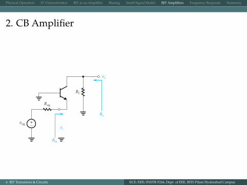
Physical Operation IV Characteristics BJT as an Amplifier Biasing Small Signal Model BJT Amplifiers Frequency Response Summary
2. CB Amplifier
vi
vo
Ro
vsig
Rsig
Rin
RC
_+
Avo = −gm (ro ‖ RC) Av = −gm (ro ‖ RC ‖ RL) Gv = Av × rπRsig+rπ
6. BJT Transistors & Circuits ECE/EEE/INSTR F244, Dept. of EEE, BITS Pilani Hyderabad Campus
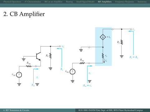
Physical Operation IV Characteristics BJT as an Amplifier Biasing Small Signal Model BJT Amplifiers Frequency Response Summary
2. CB Amplifier
vi
vo
Ro= RC
Rin= re
vsig
Rsig
RC
ie
ie
re
vi
vo
Ro
vsig
Rsig
Rin
RC
_+_+
Avo = +gmRC Av = +gm (RC ‖ RL) Gv = Av × reRsig+re
6. BJT Transistors & Circuits ECE/EEE/INSTR F244, Dept. of EEE, BITS Pilani Hyderabad Campus
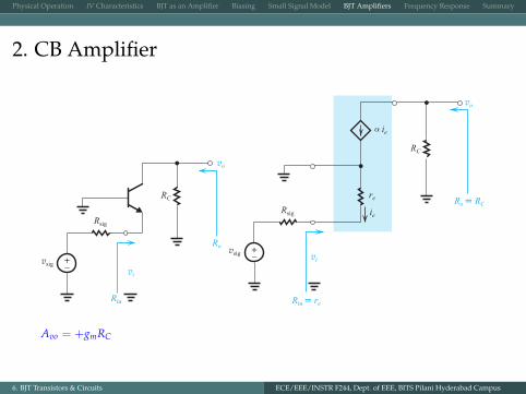
Physical Operation IV Characteristics BJT as an Amplifier Biasing Small Signal Model BJT Amplifiers Frequency Response Summary
2. CB Amplifier
vi
vo
Ro= RC
Rin= re
vsig
Rsig
RC
ie
ie
re
vi
vo
Ro
vsig
Rsig
Rin
RC
_+_+
Avo = +gmRC
Av = +gm (RC ‖ RL) Gv = Av × reRsig+re
6. BJT Transistors & Circuits ECE/EEE/INSTR F244, Dept. of EEE, BITS Pilani Hyderabad Campus
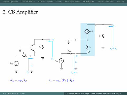
Physical Operation IV Characteristics BJT as an Amplifier Biasing Small Signal Model BJT Amplifiers Frequency Response Summary
2. CB Amplifier
vi
vo
Ro= RC
Rin= re
vsig
Rsig
RC
ie
ie
re
vi
vo
Ro
vsig
Rsig
Rin
RC
_+_+
Avo = +gmRC Av = +gm (RC ‖ RL)
Gv = Av × reRsig+re
6. BJT Transistors & Circuits ECE/EEE/INSTR F244, Dept. of EEE, BITS Pilani Hyderabad Campus

Physical Operation IV Characteristics BJT as an Amplifier Biasing Small Signal Model BJT Amplifiers Frequency Response Summary
2. CB Amplifier
vi
vo
Ro= RC
Rin= re
vsig
Rsig
RC
ie
ie
re
vi
vo
Ro
vsig
Rsig
Rin
RC
_+_+
Avo = +gmRC Av = +gm (RC ‖ RL) Gv = Av × reRsig+re
6. BJT Transistors & Circuits ECE/EEE/INSTR F244, Dept. of EEE, BITS Pilani Hyderabad Campus
Physical Operation IV Characteristics BJT as an Amplifier Biasing Small Signal Model BJT Amplifiers Frequency Response Summary
3. CC Amplifier / Emitter Follower
6. BJT Transistors & Circuits ECE/EEE/INSTR F244, Dept. of EEE, BITS Pilani Hyderabad Campus
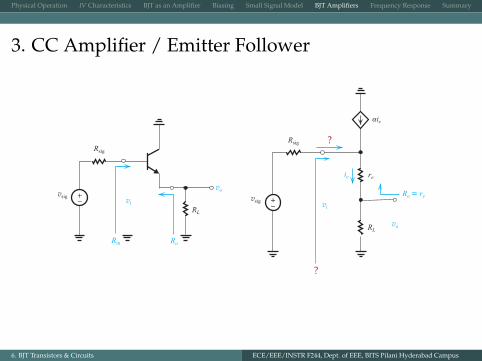
Physical Operation IV Characteristics BJT as an Amplifier Biasing Small Signal Model BJT Amplifiers Frequency Response Summary
3. CC Amplifier / Emitter Follower
vsig
Rsig
RL
RoRin
vovi_+ vsig
Rsig
re
RLvo
vi
ie
Ro= re_+
αie
?
?
Avo = 1 Av = RLre+RL
Gv = Av × RinRsig+Rin
6. BJT Transistors & Circuits ECE/EEE/INSTR F244, Dept. of EEE, BITS Pilani Hyderabad Campus
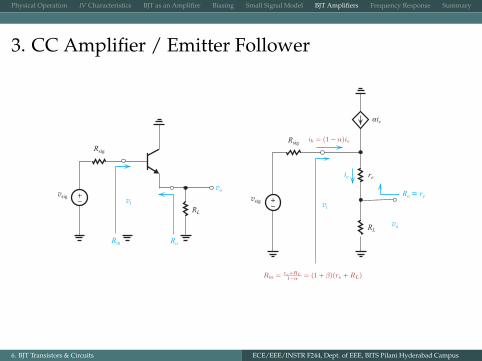
Physical Operation IV Characteristics BJT as an Amplifier Biasing Small Signal Model BJT Amplifiers Frequency Response Summary
3. CC Amplifier / Emitter Follower
vsig
Rsig
RL
RoRin
vovi_+ vsig
Rsig
re
RLvo
vi
ie
Ro= re_+
αie
Avo = 1
Av = RLre+RL
Gv = Av × RinRsig+Rin
6. BJT Transistors & Circuits ECE/EEE/INSTR F244, Dept. of EEE, BITS Pilani Hyderabad Campus
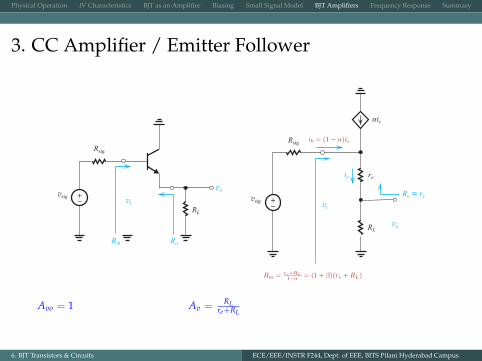
Physical Operation IV Characteristics BJT as an Amplifier Biasing Small Signal Model BJT Amplifiers Frequency Response Summary
3. CC Amplifier / Emitter Follower
vsig
Rsig
RL
RoRin
vovi_+ vsig
Rsig
re
RLvo
vi
ie
Ro= re_+
αie
Avo = 1 Av = RLre+RL
Gv = Av × RinRsig+Rin
6. BJT Transistors & Circuits ECE/EEE/INSTR F244, Dept. of EEE, BITS Pilani Hyderabad Campus
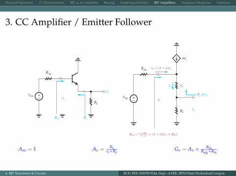
Physical Operation IV Characteristics BJT as an Amplifier Biasing Small Signal Model BJT Amplifiers Frequency Response Summary
3. CC Amplifier / Emitter Follower
vsig
Rsig
RL
RoRin
vovi_+ vsig
Rsig
re
RLvo
vi
ie
Ro= re_+
αie
Avo = 1 Av = RLre+RL
Gv = Av × RinRsig+Rin
6. BJT Transistors & Circuits ECE/EEE/INSTR F244, Dept. of EEE, BITS Pilani Hyderabad Campus
Physical Operation IV Characteristics BJT as an Amplifier Biasing Small Signal Model BJT Amplifiers Frequency Response Summary
4. CE Amplifier with Emitter Resistance
vi
vo
Rin Ro
vsig
Rsig
Re
RC
vi
vo
Rin
Ro
ic
ib
ie
vsig
Rsig B
E
C
RC
re
Re
gmvbe
_+
_+
_
+
_
+
6. BJT Transistors & Circuits ECE/EEE/INSTR F244, Dept. of EEE, BITS Pilani Hyderabad Campus
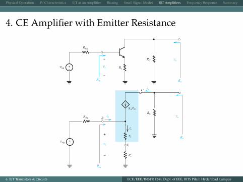
Physical Operation IV Characteristics BJT as an Amplifier Biasing Small Signal Model BJT Amplifiers Frequency Response Summary
4. CE Amplifier with Emitter Resistance ... Rin
vi
vo
Rin
Ro
ic
ib
ie
vsig
Rsig B
E
C
RC
re
Re
gmvbe
_+
_
+
ib = ie − αie = (1− α) ie
ie =vi
re + Re
Rin =viib
=vi
(1− α) ie=
vi (re + Re)
(1− α) vi= (1 + β) (re + Re)
6. BJT Transistors & Circuits ECE/EEE/INSTR F244, Dept. of EEE, BITS Pilani Hyderabad Campus
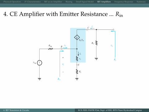
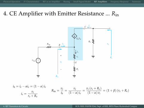

Physical Operation IV Characteristics BJT as an Amplifier Biasing Small Signal Model BJT Amplifiers Frequency Response Summary
4. CE Amplifier with Emitter Resistance ... Gains
vi
vo
Rin
Ro
ic
ib
ie
vsig
Rsig B
E
C
RC
re
Re
gmvbe
_+
_
+
vo = −gmvbeRC
gmvbe = αie = αvi
re + Re
Avo =−αRC
re + ReAv =
−α (RC ‖ RL)
re + ReGv = Av
Rin
Rsig + Rin
6. BJT Transistors & Circuits ECE/EEE/INSTR F244, Dept. of EEE, BITS Pilani Hyderabad Campus
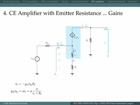
Physical Operation IV Characteristics BJT as an Amplifier Biasing Small Signal Model BJT Amplifiers Frequency Response Summary
4. CE Amplifier with Emitter Resistance ... Gains
vi
vo
Rin
Ro
ic
ib
ie
vsig
Rsig B
E
C
RC
re
Re
gmvbe
_+
_
+
vo = −gmvbeRC
gmvbe = αie = αvi
re + Re
Avo =−αRC
re + ReAv =
−α (RC ‖ RL)
re + ReGv = Av
Rin
Rsig + Rin
6. BJT Transistors & Circuits ECE/EEE/INSTR F244, Dept. of EEE, BITS Pilani Hyderabad Campus

Physical Operation IV Characteristics BJT as an Amplifier Biasing Small Signal Model BJT Amplifiers Frequency Response Summary
4. CE Amplifier with Emitter Resistance ... Gains
vi
vo
Rin
Ro
ic
ib
ie
vsig
Rsig B
E
C
RC
re
Re
gmvbe
_+
_
+
vo = −gmvbeRC
gmvbe = αie = αvi
re + Re
Avo =−αRC
re + Re
Av =−α (RC ‖ RL)
re + ReGv = Av
Rin
Rsig + Rin
6. BJT Transistors & Circuits ECE/EEE/INSTR F244, Dept. of EEE, BITS Pilani Hyderabad Campus
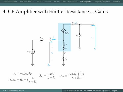
Physical Operation IV Characteristics BJT as an Amplifier Biasing Small Signal Model BJT Amplifiers Frequency Response Summary
4. CE Amplifier with Emitter Resistance ... Gains
vi
vo
Rin
Ro
ic
ib
ie
vsig
Rsig B
E
C
RC
re
Re
gmvbe
_+
_
+
vo = −gmvbeRC
gmvbe = αie = αvi
re + Re
Avo =−αRC
re + ReAv =
−α (RC ‖ RL)
re + Re
Gv = AvRin
Rsig + Rin
6. BJT Transistors & Circuits ECE/EEE/INSTR F244, Dept. of EEE, BITS Pilani Hyderabad Campus
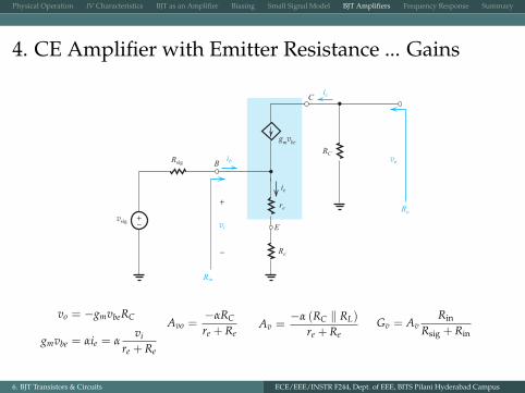
Physical Operation IV Characteristics BJT as an Amplifier Biasing Small Signal Model BJT Amplifiers Frequency Response Summary
4. CE Amplifier with Emitter Resistance ... Gains
vi
vo
Rin
Ro
ic
ib
ie
vsig
Rsig B
E
C
RC
re
Re
gmvbe
_+
_
+
vo = −gmvbeRC
gmvbe = αie = αvi
re + Re
Avo =−αRC
re + ReAv =
−α (RC ‖ RL)
re + ReGv = Av
Rin
Rsig + Rin
6. BJT Transistors & Circuits ECE/EEE/INSTR F244, Dept. of EEE, BITS Pilani Hyderabad Campus

Physical Operation IV Characteristics BJT as an Amplifier Biasing Small Signal Model BJT Amplifiers Frequency Response Summary
4. CE Amplifier with Emitter Resistance ***
6. BJT Transistors & Circuits ECE/EEE/INSTR F244, Dept. of EEE, BITS Pilani Hyderabad Campus
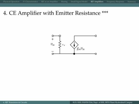
Physical Operation IV Characteristics BJT as an Amplifier Biasing Small Signal Model BJT Amplifiers Frequency Response Summary
4. CE Amplifier with Emitter Resistance ***
+
−
vbegmvbe
6. BJT Transistors & Circuits ECE/EEE/INSTR F244, Dept. of EEE, BITS Pilani Hyderabad Campus
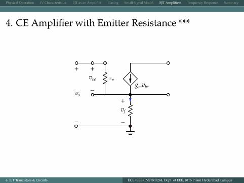
Physical Operation IV Characteristics BJT as an Amplifier Biasing Small Signal Model BJT Amplifiers Frequency Response Summary
4. CE Amplifier with Emitter Resistance ***
+
−
vbegmvbe
+
−
vs+
−
vf
6. BJT Transistors & Circuits ECE/EEE/INSTR F244, Dept. of EEE, BITS Pilani Hyderabad Campus
Physical Operation IV Characteristics BJT as an Amplifier Biasing Small Signal Model BJT Amplifiers Frequency Response Summary
4. CE Amplifier with Emitter Resistance ***
+
−
vbegmvbe
+
−
vs+ −vf
Rearranging the figure in the previous slide like the above shown gives you abetter picture of the feedback phenomena.
6. BJT Transistors & Circuits ECE/EEE/INSTR F244, Dept. of EEE, BITS Pilani Hyderabad Campus
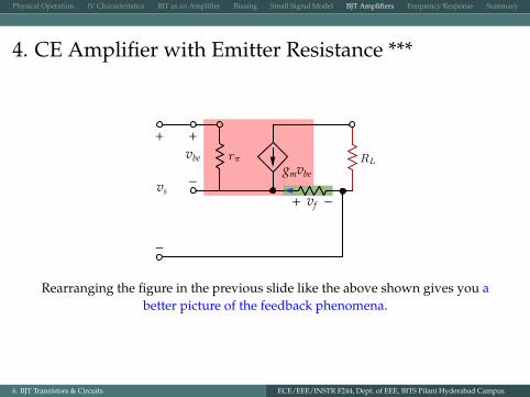

Physical Operation IV Characteristics BJT as an Amplifier Biasing Small Signal Model BJT Amplifiers Frequency Response Summary
4. CE Amplifier with Emitter Resistance ***
+
−
vsg'mvs
g′m =gm
1 + gm
(REα
)
r′π = rπ ×[
1 + gm
(REα
)]
6. BJT Transistors & Circuits ECE/EEE/INSTR F244, Dept. of EEE, BITS Pilani Hyderabad Campus
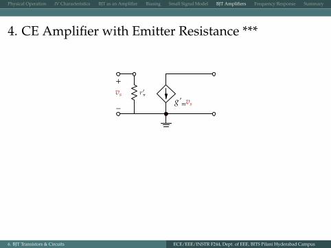
Physical Operation IV Characteristics BJT as an Amplifier Biasing Small Signal Model BJT Amplifiers Frequency Response Summary
4. CE Amplifier with Emitter Resistance ***
+
−
vsg'mvs
g′m =gm
1 + gm
(REα
)
r′π = rπ ×[
1 + gm
(REα
)]
6. BJT Transistors & Circuits ECE/EEE/INSTR F244, Dept. of EEE, BITS Pilani Hyderabad Campus
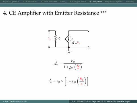
Physical Operation IV Characteristics BJT as an Amplifier Biasing Small Signal Model BJT Amplifiers Frequency Response Summary
4. CE Amplifier with Emitter Resistance ***
+
−
vsg'mvs
g′m =gm
1 + gm
(REα
)
r′π = rπ ×[
1 + gm
(REα
)]
6. BJT Transistors & Circuits ECE/EEE/INSTR F244, Dept. of EEE, BITS Pilani Hyderabad Campus
Physical Operation IV Characteristics BJT as an Amplifier Biasing Small Signal Model BJT Amplifiers Frequency Response Summary
BJT Amplifiers – Summary
Type Ri Ro Avo Av Gv
CE rπ RC −gm (ro ‖ RC) −gm (ro ‖ RC ‖ RL) AvRin
Rin+Rsig
CB re RC +gm (ro ‖ RC) +gm (ro ‖ RC ‖ RL) AvRin
Rin+Rsig
CC (1 + β) (re + RL)* re 1 RLRL+re
AvRin
Rin+Rsig
CE with Re (1 + β) (re + Re) RC−αRCre+Re
−α(RC‖RL)re+Re
AvRin
Rin+Rsig
6. BJT Transistors & Circuits ECE/EEE/INSTR F244, Dept. of EEE, BITS Pilani Hyderabad Campus
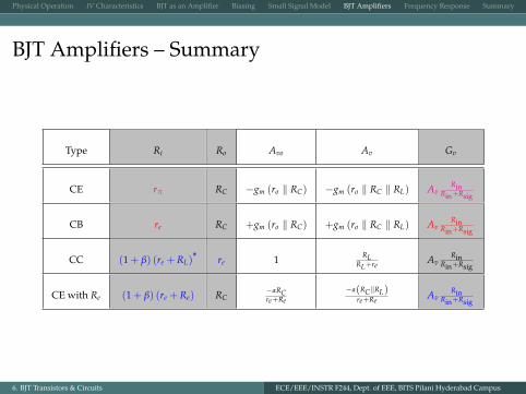

Physical Operation IV Characteristics BJT as an Amplifier Biasing Small Signal Model BJT Amplifiers Frequency Response Summary
Outline
1 Physical Operation
2 IV Characteristics
3 BJT as an Amplifier
4 Biasing
5 Small Signal Model
6 BJT Amplifiers
7 Frequency Response
8 Summary
6. BJT Transistors & Circuits ECE/EEE/INSTR F244, Dept. of EEE, BITS Pilani Hyderabad Campus
Physical Operation IV Characteristics BJT as an Amplifier Biasing Small Signal Model BJT Amplifiers Frequency Response Summary
BJT Internal Capacitances & High Frequency Model
n-type n-type
Emitterregion
Emitter–basejunction(EBJ)
Collector–basejunction(CBJ)
Collector(C)
Emitter(E)
Metalcontact
Collectorregion
p-type
Baseregion
Base(B)
gmro
rx
6. BJT Transistors & Circuits ECE/EEE/INSTR F244, Dept. of EEE, BITS Pilani Hyderabad Campus
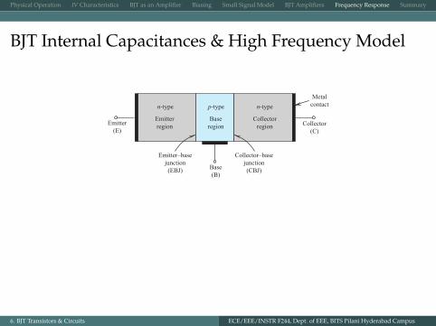
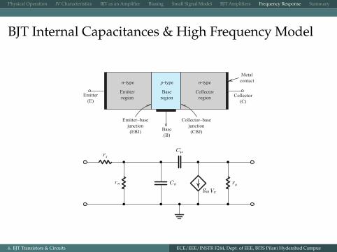

Physical Operation IV Characteristics BJT as an Amplifier Biasing Small Signal Model BJT Amplifiers Frequency Response Summary
Unity Gain Bandwidth (ωT)
gmro
rx
Vπ =Ib
1rπ
+ s(Cµ + Cπ
)Ie = gmVπ = gm
Ib1
rπ+ s
(Cµ + Cπ
)
Ie
Ib=
gmrπ
1 + srπ
(Cµ + Cπ
) =β0
1 + srπ
(Cµ + Cπ
)ωβ =
1rπ
(Cµ + Cπ
)ωT =
gm
Cµ + Cπ
6. BJT Transistors & Circuits ECE/EEE/INSTR F244, Dept. of EEE, BITS Pilani Hyderabad Campus
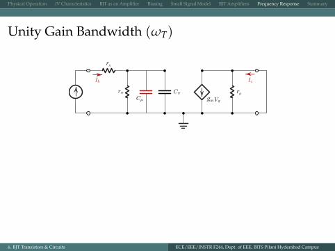
Physical Operation IV Characteristics BJT as an Amplifier Biasing Small Signal Model BJT Amplifiers Frequency Response Summary
Unity Gain Bandwidth (ωT)
gmro
rx
Vπ =Ib
1rπ
+ s(Cµ + Cπ
)Ic = gmVπ = gm
Ib1
rπ+ s
(Cµ + Cπ
)
Ic
Ib=
gmrπ
1 + srπ
(Cµ + Cπ
) =β0
1 + srπ
(Cµ + Cπ
)ωβ =
1rπ
(Cµ + Cπ
)ωT =
gm
Cµ + Cπ
6. BJT Transistors & Circuits ECE/EEE/INSTR F244, Dept. of EEE, BITS Pilani Hyderabad Campus

Physical Operation IV Characteristics BJT as an Amplifier Biasing Small Signal Model BJT Amplifiers Frequency Response Summary
Unity Gain Bandwidth (ωT)
gmro
rx
Vπ =Ib
1rπ
+ s(Cµ + Cπ
)
Ic = gmVπ = gmIb
1rπ
+ s(Cµ + Cπ
)
Ic
Ib=
gmrπ
1 + srπ
(Cµ + Cπ
) =β0
1 + srπ
(Cµ + Cπ
)ωβ =
1rπ
(Cµ + Cπ
)ωT =
gm
Cµ + Cπ
6. BJT Transistors & Circuits ECE/EEE/INSTR F244, Dept. of EEE, BITS Pilani Hyderabad Campus
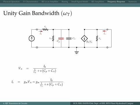
Physical Operation IV Characteristics BJT as an Amplifier Biasing Small Signal Model BJT Amplifiers Frequency Response Summary
Unity Gain Bandwidth (ωT)
gmro
rx
Vπ =Ib
1rπ
+ s(Cµ + Cπ
)Ic = gmVπ = gm
Ib1
rπ+ s
(Cµ + Cπ
)
Ic
Ib=
gmrπ
1 + srπ
(Cµ + Cπ
) =β0
1 + srπ
(Cµ + Cπ
)ωβ =
1rπ
(Cµ + Cπ
)ωT =
gm
Cµ + Cπ
6. BJT Transistors & Circuits ECE/EEE/INSTR F244, Dept. of EEE, BITS Pilani Hyderabad Campus
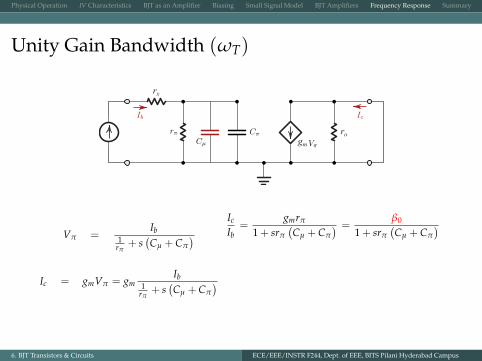
Physical Operation IV Characteristics BJT as an Amplifier Biasing Small Signal Model BJT Amplifiers Frequency Response Summary
Unity Gain Bandwidth (ωT)
gmro
rx
Vπ =Ib
1rπ
+ s(Cµ + Cπ
)Ic = gmVπ = gm
Ib1
rπ+ s
(Cµ + Cπ
)
Ic
Ib=
gmrπ
1 + srπ
(Cµ + Cπ
) =β0
1 + srπ
(Cµ + Cπ
)
ωβ =1
rπ
(Cµ + Cπ
)ωT =
gm
Cµ + Cπ
6. BJT Transistors & Circuits ECE/EEE/INSTR F244, Dept. of EEE, BITS Pilani Hyderabad Campus

Physical Operation IV Characteristics BJT as an Amplifier Biasing Small Signal Model BJT Amplifiers Frequency Response Summary
Unity Gain Bandwidth (ωT)
gmro
rx
Vπ =Ib
1rπ
+ s(Cµ + Cπ
)Ic = gmVπ = gm
Ib1
rπ+ s
(Cµ + Cπ
)
Ic
Ib=
gmrπ
1 + srπ
(Cµ + Cπ
) =β0
1 + srπ
(Cµ + Cπ
)ωβ =
1rπ
(Cµ + Cπ
)
ωT =gm
Cµ + Cπ
6. BJT Transistors & Circuits ECE/EEE/INSTR F244, Dept. of EEE, BITS Pilani Hyderabad Campus
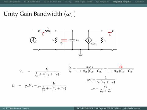
Physical Operation IV Characteristics BJT as an Amplifier Biasing Small Signal Model BJT Amplifiers Frequency Response Summary
Unity Gain Bandwidth (ωT)
gmro
rx
Vπ =Ib
1rπ
+ s(Cµ + Cπ
)Ic = gmVπ = gm
Ib1
rπ+ s
(Cµ + Cπ
)
Ic
Ib=
gmrπ
1 + srπ
(Cµ + Cπ
) =β0
1 + srπ
(Cµ + Cπ
)ωβ =
1rπ
(Cµ + Cπ
)ωT =
gm
Cµ + Cπ
6. BJT Transistors & Circuits ECE/EEE/INSTR F244, Dept. of EEE, BITS Pilani Hyderabad Campus

Physical Operation IV Characteristics BJT as an Amplifier Biasing Small Signal Model BJT Amplifiers Frequency Response Summary
Frequency Response of CE Amplifier
VEE
VCC
CC1
CE
Rsig
Vsig
Vo
RL
CC2
I
RB
RC
_+
_
6. BJT Transistors & Circuits ECE/EEE/INSTR F244, Dept. of EEE, BITS Pilani Hyderabad Campus
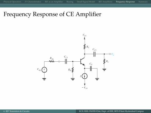
Physical Operation IV Characteristics BJT as an Amplifier Biasing Small Signal Model BJT Amplifiers Frequency Response Summary
Frequency Response of CE Amplifier
VEE
VCC
CC1
CE
Rsig
Vsig
Vo
RL
CC2
I
RB
RC
_+
_
6. BJT Transistors & Circuits ECE/EEE/INSTR F244, Dept. of EEE, BITS Pilani Hyderabad Campus
Physical Operation IV Characteristics BJT as an Amplifier Biasing Small Signal Model BJT Amplifiers Frequency Response Summary
Frequency Response of CE Amplifier
Vo(dB)
Low-frequencyband
ViMidband
All capacitances can be neglected
High-frequency band
Gain falls offdue to the effectof Ci , CSand Co
3 dB
20 log |AM| (dB)
fL fH f (Hz)
Gain falls offdue to the internalcapacitive effectsof the MOSFET
6. BJT Transistors & Circuits ECE/EEE/INSTR F244, Dept. of EEE, BITS Pilani Hyderabad Campus
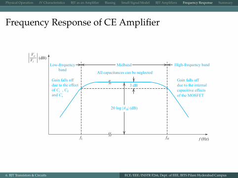

Physical Operation IV Characteristics BJT as an Amplifier Biasing Small Signal Model BJT Amplifiers Frequency Response Summary
High Frequency Response of CE Amplifier
RB
Rsig
Vsiggm
Voro RC RL
rx
R 'L
_+_
+
_
+
Applying Miller’s theorem gives time constant,
τ ={[(
Rsig ‖ RB)+ rx
]‖ rπ
} [Cπ + gmR′LCµ
]. (18)
So, for the CE amplifier fH is given as
fH =1
2πτ=
12π{[(
Rsig ‖ RB)+ rx
]‖ rπ
} [Cπ + gmR′LCµ
] . (19)
6. BJT Transistors & Circuits ECE/EEE/INSTR F244, Dept. of EEE, BITS Pilani Hyderabad Campus
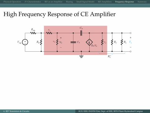
Physical Operation IV Characteristics BJT as an Amplifier Biasing Small Signal Model BJT Amplifiers Frequency Response Summary
High Frequency Response of CE Amplifier
RB
Rsig
Vsiggm
Voro RC RL
rx
R 'L
_+_
+
_
+
Applying Miller’s theorem gives time constant,
τ ={[(
Rsig ‖ RB)+ rx
]‖ rπ
} [Cπ + gmR′LCµ
]. (18)
So, for the CE amplifier fH is given as
fH =1
2πτ=
12π{[(
Rsig ‖ RB)+ rx
]‖ rπ
} [Cπ + gmR′LCµ
] . (19)
6. BJT Transistors & Circuits ECE/EEE/INSTR F244, Dept. of EEE, BITS Pilani Hyderabad Campus
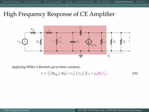
Physical Operation IV Characteristics BJT as an Amplifier Biasing Small Signal Model BJT Amplifiers Frequency Response Summary
High Frequency Response of CE Amplifier
RB
Rsig
Vsiggm
Voro RC RL
rx
R 'L
_+_
+
_
+
Applying Miller’s theorem gives time constant,
τ ={[(
Rsig ‖ RB)+ rx
]‖ rπ
} [Cπ + gmR′LCµ
]. (18)
So, for the CE amplifier fH is given as
fH =1
2πτ=
12π{[(
Rsig ‖ RB)+ rx
]‖ rπ
} [Cπ + gmR′LCµ
] . (19)
6. BJT Transistors & Circuits ECE/EEE/INSTR F244, Dept. of EEE, BITS Pilani Hyderabad Campus
Physical Operation IV Characteristics BJT as an Amplifier Biasing Small Signal Model BJT Amplifiers Frequency Response Summary
High Frequency Response of CE Amplifier
RB
Rsig
Vsiggm
Voro RC RL
rx
R 'L
_+_
+
_
+
So, the total high frequency response is given as
Vo (s)Vi (s)
= AM1
1 + sτ, (20)
where τ ={[(
Rsig ‖ RB)+ rx
]‖ rπ
} [Cπ + gmR′LCµ
]and AM = −gm (ro ‖ RC ‖ RL).
6. BJT Transistors & Circuits ECE/EEE/INSTR F244, Dept. of EEE, BITS Pilani Hyderabad Campus
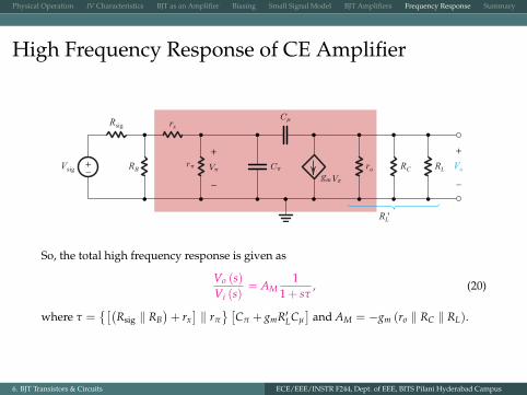

Physical Operation IV Characteristics BJT as an Amplifier Biasing Small Signal Model BJT Amplifiers Frequency Response Summary
Low Frequency Response of CE Amplifier
−+
gmvbe
vbe rπ
6. BJT Transistors & Circuits ECE/EEE/INSTR F244, Dept. of EEE, BITS Pilani Hyderabad Campus
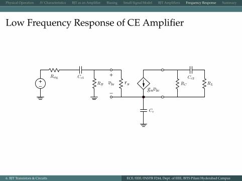
Physical Operation IV Characteristics BJT as an Amplifier Biasing Small Signal Model BJT Amplifiers Frequency Response Summary
Low Frequency Response of CE Amplifier
−+
gmvbe
vbe rπ
6. BJT Transistors & Circuits ECE/EEE/INSTR F244, Dept. of EEE, BITS Pilani Hyderabad Campus
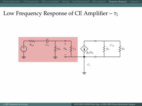
Physical Operation IV Characteristics BJT as an Amplifier Biasing Small Signal Model BJT Amplifiers Frequency Response Summary
Low Frequency Response of CE Amplifier – τ1
−+
gmvbe
vbe rπ
6. BJT Transistors & Circuits ECE/EEE/INSTR F244, Dept. of EEE, BITS Pilani Hyderabad Campus

Physical Operation IV Characteristics BJT as an Amplifier Biasing Small Signal Model BJT Amplifiers Frequency Response Summary
Low Frequency Response of CE Amplifier – τ2
−+
gmvbe
vbe rπ
6. BJT Transistors & Circuits ECE/EEE/INSTR F244, Dept. of EEE, BITS Pilani Hyderabad Campus

Physical Operation IV Characteristics BJT as an Amplifier Biasing Small Signal Model BJT Amplifiers Frequency Response Summary
Low Frequency Response of CE Amplifier – τ3
−+
gmvbe
vbe rπ
6. BJT Transistors & Circuits ECE/EEE/INSTR F244, Dept. of EEE, BITS Pilani Hyderabad Campus
Physical Operation IV Characteristics BJT as an Amplifier Biasing Small Signal Model BJT Amplifiers Frequency Response Summary
Low Frequency Response of CE Amplifier
−+
gmvbe
vbe rπ
So, the total low frequency response is given as
Vo (s)Vi (s)
= AM ×sτ1
1 + sτ1× sτ2
1 + sτ2× sτ3
1 + sτ3, (21)
where AM = −gm (RC ‖ RL).
6. BJT Transistors & Circuits ECE/EEE/INSTR F244, Dept. of EEE, BITS Pilani Hyderabad Campus
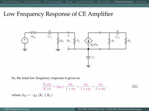
Physical Operation IV Characteristics BJT as an Amplifier Biasing Small Signal Model BJT Amplifiers Frequency Response Summary
Outline
1 Physical Operation
2 IV Characteristics
3 BJT as an Amplifier
4 Biasing
5 Small Signal Model
6 BJT Amplifiers
7 Frequency Response
8 Summary
6. BJT Transistors & Circuits ECE/EEE/INSTR F244, Dept. of EEE, BITS Pilani Hyderabad Campus
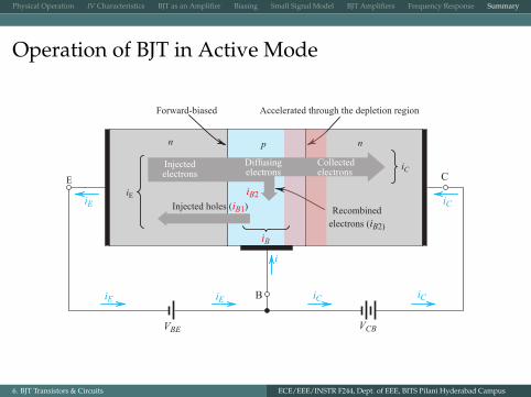
Physical Operation IV Characteristics BJT as an Amplifier Biasing Small Signal Model BJT Amplifiers Frequency Response Summary
Operation of BJT in Active Mode
B
C
iEiE iC iC
i
iB
iB2iCiE
Recombinedelectrons (iB2)
Injected holes (iB1
E
Forward-biased
iE
iC
n p n
Accelerated through the depletion region
VBE
(
Injectedelectrons
Diffusingelectrons
Collectedelectrons
VCB
6. BJT Transistors & Circuits ECE/EEE/INSTR F244, Dept. of EEE, BITS Pilani Hyderabad Campus
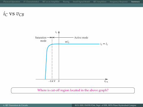
Physical Operation IV Characteristics BJT as an Amplifier Biasing Small Signal Model BJT Amplifiers Frequency Response Summary
iC vs vCB
vCB
Saturationmode
Active mode
α IE iE= IE
- 0.4 V
iC
0�� ��Where is cut-off region located in the above graph?
6. BJT Transistors & Circuits ECE/EEE/INSTR F244, Dept. of EEE, BITS Pilani Hyderabad Campus
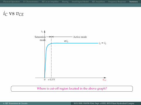
Physical Operation IV Characteristics BJT as an Amplifier Biasing Small Signal Model BJT Amplifiers Frequency Response Summary
iC vs vCE
vCE
Saturationmode
Active mode
α IE iE= IE
+ 0.3 V
iC
0�� ��Where is cut-off region located in the above graph?
6. BJT Transistors & Circuits ECE/EEE/INSTR F244, Dept. of EEE, BITS Pilani Hyderabad Campus
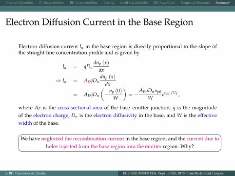
Physical Operation IV Characteristics BJT as an Amplifier Biasing Small Signal Model BJT Amplifiers Frequency Response Summary
Electron Diffusion Current in the Base Region
Electron diffusion current In in the base region is directly proportional to the slope ofthe straight-line concentration profile and is given by
Jn = qDndnp (x)
dx
⇒ In = AEqDndnp (x)
dx
= AEqDn
(−
np (0)W
)= −
AEqDnnp0
WevBE/VT ,
where AE is the cross-sectional area of the base–emitter junction, q is the magnitudeof the electron charge, Dn is the electron diffusivity in the base, and W is the effectivewidth of the base.�
�We have neglected the recombination current in the base region, and the current due to
holes injected from the base region into the emitter region. Why?
6. BJT Transistors & Circuits ECE/EEE/INSTR F244, Dept. of EEE, BITS Pilani Hyderabad Campus
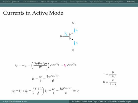
Physical Operation IV Characteristics BJT as an Amplifier Biasing Small Signal Model BJT Amplifiers Frequency Response Summary
Currents in Active Mode
B
C
E
iC
iE
iB
iC = −In =
(AEqDnnp0
W
)evBE/VT = IS evBE/VT
iB =iCβ
=ISevBE/VT
β
iE = iC + iB =
(β + 1
β
)iC =
iCα
=ISevBE/VT
α≈ iC
α =β
1 + β
β =α
1− α
6. BJT Transistors & Circuits ECE/EEE/INSTR F244, Dept. of EEE, BITS Pilani Hyderabad Campus

Physical Operation IV Characteristics BJT as an Amplifier Biasing Small Signal Model BJT Amplifiers Frequency Response Summary
MOSFET vs BJT
n+
L
Metal
Channelregion
Oxide (SiO2)(thickness = tox)
p-type substrate(Body)
n+
Source (S) Gate (G) Drain (D)
Bod y (B)
n-type n-type
Emitterregion
Emitter–basejunction(EBJ)
Collector–basejunction(CBJ)
Collector(C)
Emitter(E)
Metalcontact
Collectorregion
p-type
Baseregion
Base(B)
vCE
Saturationmode
Active mode
α IE iE= IE
+ 0.3 V
iC
0
iD
vDS sat =
vGS = +Vt
0
Triode Saturation
vOV
Current saturates because thechannel is pinched off at thedrain end, and vDS no longeraffects the channel.
vDSvOV
6. BJT Transistors & Circuits ECE/EEE/INSTR F244, Dept. of EEE, BITS Pilani Hyderabad Campus
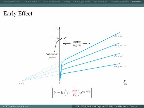
Physical Operation IV Characteristics BJT as an Amplifier Biasing Small Signal Model BJT Amplifiers Frequency Response Summary
Early Effect
vCE
iC
0
Saturationregion
Activeregion
-VA
iC = IS
(1 +
vCE
VA
)evBE/VT
6. BJT Transistors & Circuits ECE/EEE/INSTR F244, Dept. of EEE, BITS Pilani Hyderabad Campus

Physical Operation IV Characteristics BJT as an Amplifier Biasing Small Signal Model BJT Amplifiers Frequency Response Summary
1. Biasing by Fixing VBE (Bad)
RB2
RB1
VBE
RC
VCC
IC
IBVCE
RB RC
VCC
IC
IB
VCE
VBE
+ +
6. BJT Transistors & Circuits ECE/EEE/INSTR F244, Dept. of EEE, BITS Pilani Hyderabad Campus
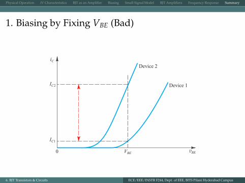
Physical Operation IV Characteristics BJT as an Amplifier Biasing Small Signal Model BJT Amplifiers Frequency Response Summary
1. Biasing by Fixing VBE (Bad)
iC
vBEVBE
IC1
0
IC2
Device 2
Device 1
6. BJT Transistors & Circuits ECE/EEE/INSTR F244, Dept. of EEE, BITS Pilani Hyderabad Campus
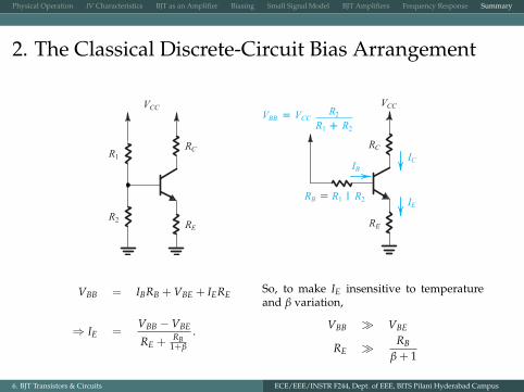
Physical Operation IV Characteristics BJT as an Amplifier Biasing Small Signal Model BJT Amplifiers Frequency Response Summary
2. The Classical Discrete-Circuit Bias Arrangement
R1
RER2
VCC
RC
VBB VCCR1 R2
R2
RB R1 R2
IB
IE
IC
=
RC
RE
VCC
=
+
VBB = IBRB + VBE + IERE
⇒ IE =VBB −VBE
RE + RB1+β
.
So, to make IE insensitive to temperatureand β variation,
VBB � VBE
RE � RB
β + 1
6. BJT Transistors & Circuits ECE/EEE/INSTR F244, Dept. of EEE, BITS Pilani Hyderabad Campus
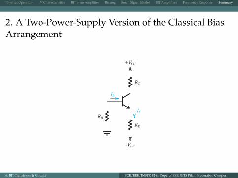
Physical Operation IV Characteristics BJT as an Amplifier Biasing Small Signal Model BJT Amplifiers Frequency Response Summary
2. A Two-Power-Supply Version of the Classical BiasArrangement
RE
RB
+VCC
RC
-VEE
IB
IE
6. BJT Transistors & Circuits ECE/EEE/INSTR F244, Dept. of EEE, BITS Pilani Hyderabad Campus
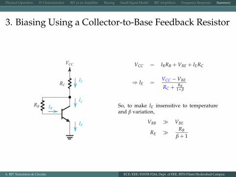
Physical Operation IV Characteristics BJT as an Amplifier Biasing Small Signal Model BJT Amplifiers Frequency Response Summary
3. Biasing Using a Collector-to-Base Feedback Resistor
IB
IE
IC
RC
VCC
RB
IE
VCC = IBRB + VBE + IERC
⇒ IE =VCC −VBE
RC + RB1+β
So, to make IE insensitive to temperatureand β variation,
VBB � VBE
RE � RB
β + 1
6. BJT Transistors & Circuits ECE/EEE/INSTR F244, Dept. of EEE, BITS Pilani Hyderabad Campus
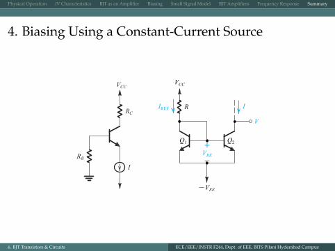
Physical Operation IV Characteristics BJT as an Amplifier Biasing Small Signal Model BJT Amplifiers Frequency Response Summary
4. Biasing Using a Constant-Current Source
6. BJT Transistors & Circuits ECE/EEE/INSTR F244, Dept. of EEE, BITS Pilani Hyderabad Campus
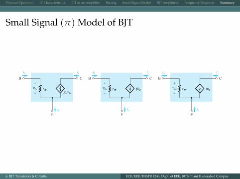
Physical Operation IV Characteristics BJT as an Amplifier Biasing Small Signal Model BJT Amplifiers Frequency Response Summary
Small Signal (π) Model of BJT
E
B C+
–
ib ic
ie
vbegmvbe
rπ
E
B C+
–
ib ic
ie
vbe rπ β iB
E
B C+
–
ib ic
ie
vbe rπ αiE
6. BJT Transistors & Circuits ECE/EEE/INSTR F244, Dept. of EEE, BITS Pilani Hyderabad Campus
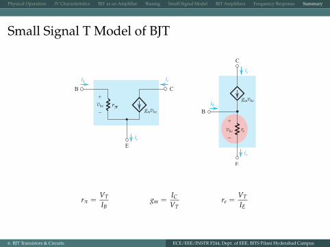
Physical Operation IV Characteristics BJT as an Amplifier Biasing Small Signal Model BJT Amplifiers Frequency Response Summary
Small Signal T Model of BJT
E
B C+
–
ib ic
ie
vbegmvbe
rπ
C
B
E
ic
ib
re
ie
gmvbe
+
–
vbe
rπ =VT
IBgm =
IC
VTre =
VT
IE
6. BJT Transistors & Circuits ECE/EEE/INSTR F244, Dept. of EEE, BITS Pilani Hyderabad Campus

Physical Operation IV Characteristics BJT as an Amplifier Biasing Small Signal Model BJT Amplifiers Frequency Response Summary
Small Signal Model (Including Early Effect)
gm = IC /VTrπ = IBVT/
E
B C+
–
ib ic
ie
vbegmvbe
rπ ro
E
B C+
–
ib ic
ie
vbe rπ roβ iB
ro =VA
I′C,≈ VA
IC
where I′C is the value of the collector current with the Early effect neglected.
6. BJT Transistors & Circuits ECE/EEE/INSTR F244, Dept. of EEE, BITS Pilani Hyderabad Campus
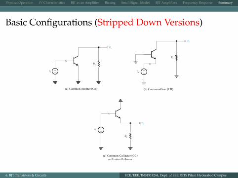
Physical Operation IV Characteristics BJT as an Amplifier Biasing Small Signal Model BJT Amplifiers Frequency Response Summary
Basic Configurations (Stripped Down Versions)
vi
RL
(c) Common-Collector (CC)or Emitter Follower
vo
_+
vi
RC
(a) Common-Emitter (CE)
vo
_+ vi
RC
(b) Common-Base (CB)
vo
_+
6. BJT Transistors & Circuits ECE/EEE/INSTR F244, Dept. of EEE, BITS Pilani Hyderabad Campus
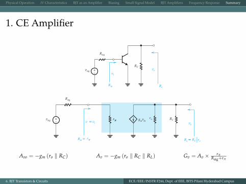
Physical Operation IV Characteristics BJT as an Amplifier Biasing Small Signal Model BJT Amplifiers Frequency Response Summary
1. CE Amplifier
vi
Rin Ro
voRC
vsig
Rsig
v = vi
Rin=
vsig
Rsig
vo
Ro= RC||ro
gmvbeRCro
_+
_+ rπ
rπ
Avo = −gm (ro ‖ RC) Av = −gm (ro ‖ RC ‖ RL) Gv = Av × rπRsig+rπ
6. BJT Transistors & Circuits ECE/EEE/INSTR F244, Dept. of EEE, BITS Pilani Hyderabad Campus
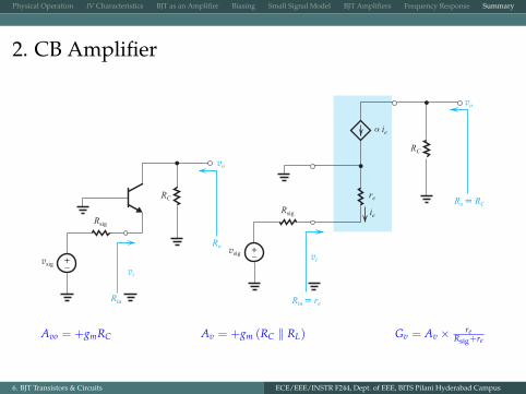
Physical Operation IV Characteristics BJT as an Amplifier Biasing Small Signal Model BJT Amplifiers Frequency Response Summary
2. CB Amplifier
vi
vo
Ro= RC
Rin= re
vsig
Rsig
RC
ie
ie
re
vi
vo
Ro
vsig
Rsig
Rin
RC
_+_+
Avo = +gmRC Av = +gm (RC ‖ RL) Gv = Av × reRsig+re
6. BJT Transistors & Circuits ECE/EEE/INSTR F244, Dept. of EEE, BITS Pilani Hyderabad Campus
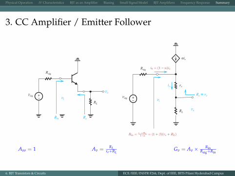
Physical Operation IV Characteristics BJT as an Amplifier Biasing Small Signal Model BJT Amplifiers Frequency Response Summary
3. CC Amplifier / Emitter Follower
vsig
Rsig
RL
RoRin
vovi_+ vsig
Rsig
re
RLvo
vi
ie
Ro= re_+
αie
Avo = 1 Av = RLre+RL
Gv = Av × RinRsig+Rin
6. BJT Transistors & Circuits ECE/EEE/INSTR F244, Dept. of EEE, BITS Pilani Hyderabad Campus

Physical Operation IV Characteristics BJT as an Amplifier Biasing Small Signal Model BJT Amplifiers Frequency Response Summary
4. CE Amplifier with Emitter Resistance ... Rin
vi
vo
Rin
Ro
ic
ib
ie
vsig
Rsig B
E
C
RC
re
Re
gmvbe
_+
_
+
ib = ie − αie = (1− α) ie
ie =vi
re + Re
Rin =viib
=vi
(1− α) ie=
vi (re + Re)
(1− α) vi= (1 + β) (re + Re)
6. BJT Transistors & Circuits ECE/EEE/INSTR F244, Dept. of EEE, BITS Pilani Hyderabad Campus
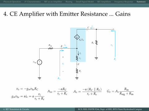
Physical Operation IV Characteristics BJT as an Amplifier Biasing Small Signal Model BJT Amplifiers Frequency Response Summary
4. CE Amplifier with Emitter Resistance ... Gains
vi
vo
Rin
Ro
ic
ib
ie
vsig
Rsig B
E
C
RC
re
Re
gmvbe
_+
_
+
vo = −gmvbeRC
gmvbe = αie = αvi
re + Re
Avo =−αRC
re + ReAv =
−α (RC ‖ RL)
re + ReGv = Av
Rin
Rsig + Rin
6. BJT Transistors & Circuits ECE/EEE/INSTR F244, Dept. of EEE, BITS Pilani Hyderabad Campus
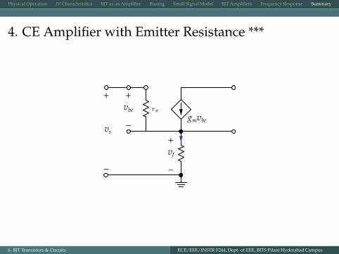
Physical Operation IV Characteristics BJT as an Amplifier Biasing Small Signal Model BJT Amplifiers Frequency Response Summary
4. CE Amplifier with Emitter Resistance ***
+
−
vbegmvbe
+
−
vs+
−
vf
6. BJT Transistors & Circuits ECE/EEE/INSTR F244, Dept. of EEE, BITS Pilani Hyderabad Campus
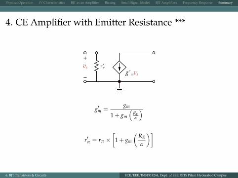
Physical Operation IV Characteristics BJT as an Amplifier Biasing Small Signal Model BJT Amplifiers Frequency Response Summary
4. CE Amplifier with Emitter Resistance ***
+
−
vsg'mvs
g′m =gm
1 + gm
(REα
)
r′π = rπ ×[
1 + gm
(REα
)]
6. BJT Transistors & Circuits ECE/EEE/INSTR F244, Dept. of EEE, BITS Pilani Hyderabad Campus
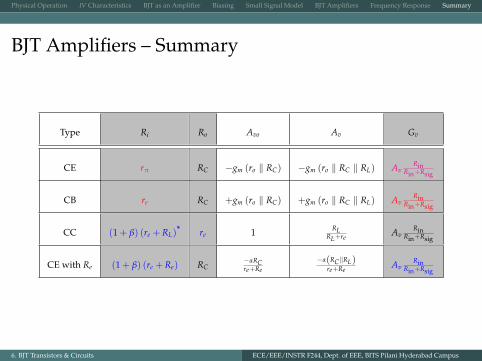
Physical Operation IV Characteristics BJT as an Amplifier Biasing Small Signal Model BJT Amplifiers Frequency Response Summary
BJT Amplifiers – Summary
Type Ri Ro Avo Av Gv
CE rπ RC −gm (ro ‖ RC) −gm (ro ‖ RC ‖ RL) AvRin
Rin+Rsig
CB re RC +gm (ro ‖ RC) +gm (ro ‖ RC ‖ RL) AvRin
Rin+Rsig
CC (1 + β) (re + RL)* re 1 RLRL+re
AvRin
Rin+Rsig
CE with Re (1 + β) (re + Re) RC−αRCre+Re
−α(RC‖RL)re+Re
AvRin
Rin+Rsig
6. BJT Transistors & Circuits ECE/EEE/INSTR F244, Dept. of EEE, BITS Pilani Hyderabad Campus
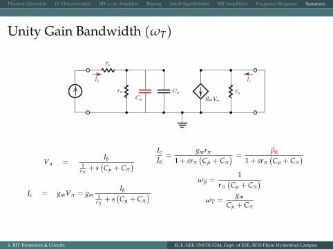
Physical Operation IV Characteristics BJT as an Amplifier Biasing Small Signal Model BJT Amplifiers Frequency Response Summary
Unity Gain Bandwidth (ωT)
gmro
rx
Vπ =Ib
1rπ
+ s(Cµ + Cπ
)Ic = gmVπ = gm
Ib1
rπ+ s
(Cµ + Cπ
)
Ic
Ib=
gmrπ
1 + srπ
(Cµ + Cπ
) =β0
1 + srπ
(Cµ + Cπ
)ωβ =
1rπ
(Cµ + Cπ
)ωT =
gm
Cµ + Cπ
6. BJT Transistors & Circuits ECE/EEE/INSTR F244, Dept. of EEE, BITS Pilani Hyderabad Campus

Physical Operation IV Characteristics BJT as an Amplifier Biasing Small Signal Model BJT Amplifiers Frequency Response Summary
High Frequency Response of CE Amplifier
RB
Rsig
Vsiggm
Voro RC RL
rx
R 'L
_+_
+
_
+
So, the total high frequency response is given as
Vo (s)Vi (s)
= AM1
1 + sτ,
where τ ={[(
Rsig ‖ RB)+ rx
]‖ rπ
} [Cπ + gmR′LCµ
]and AM = −gm (ro ‖ RC ‖ RL).
6. BJT Transistors & Circuits ECE/EEE/INSTR F244, Dept. of EEE, BITS Pilani Hyderabad Campus

Physical Operation IV Characteristics BJT as an Amplifier Biasing Small Signal Model BJT Amplifiers Frequency Response Summary
Low Frequency Response of CE Amplifier – τ1
−+
gmvbe
vbe rπ
6. BJT Transistors & Circuits ECE/EEE/INSTR F244, Dept. of EEE, BITS Pilani Hyderabad Campus
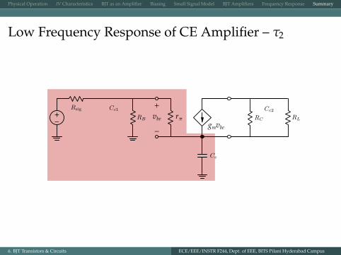
Physical Operation IV Characteristics BJT as an Amplifier Biasing Small Signal Model BJT Amplifiers Frequency Response Summary
Low Frequency Response of CE Amplifier – τ2
−+
gmvbe
vbe rπ
6. BJT Transistors & Circuits ECE/EEE/INSTR F244, Dept. of EEE, BITS Pilani Hyderabad Campus
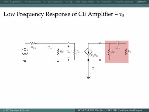
Physical Operation IV Characteristics BJT as an Amplifier Biasing Small Signal Model BJT Amplifiers Frequency Response Summary
Low Frequency Response of CE Amplifier – τ3
−+
gmvbe
vbe rπ
6. BJT Transistors & Circuits ECE/EEE/INSTR F244, Dept. of EEE, BITS Pilani Hyderabad Campus
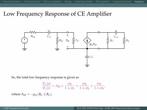
Physical Operation IV Characteristics BJT as an Amplifier Biasing Small Signal Model BJT Amplifiers Frequency Response Summary
Low Frequency Response of CE Amplifier
−+
gmvbe
vbe rπ
So, the total low frequency response is given as
Vo (s)Vi (s)
= AM ×sτ1
1 + sτ1× sτ2
1 + sτ2× sτ3
1 + sτ3,
where AM = −gm (RC ‖ RL).
6. BJT Transistors & Circuits ECE/EEE/INSTR F244, Dept. of EEE, BITS Pilani Hyderabad Campus
Related Documents