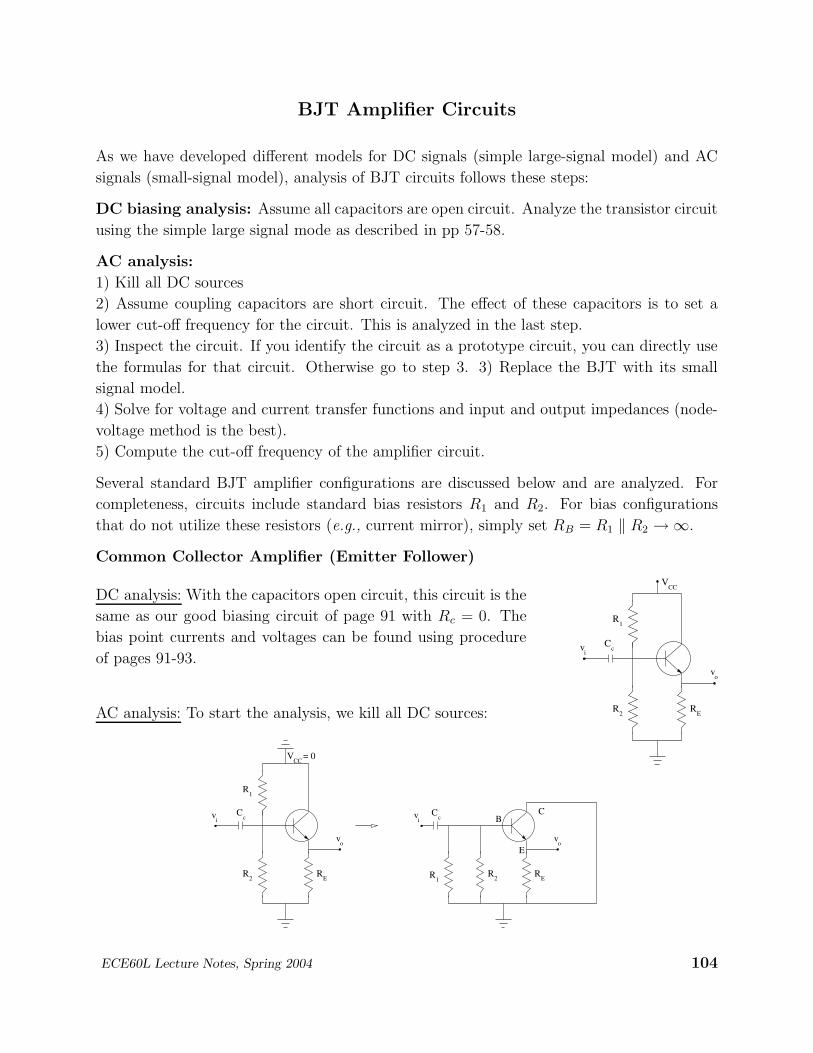
BJT Amplifier Circuits As we have developed different models for DC signals (simple large-signal model) and AC signals (small-signal model), analysis of BJT circuits follows these steps: DC biasing analysis: Assume all capacitors are open circuit. Analyze the transistor circuit using the simple large signal mode as described in pp 57-58. AC analysis: 1) Kill all DC sources 2) Assume coupling capacitors are short circuit. The effect of these capacitors is to set a lower cut-off frequency for the circuit. This is analyzed in the last step. 3) Inspect the circuit. If you identify the circuit as a prototype circuit, you can directly use the formulas for that circuit. Otherwise go to step 3. 3) Replace the BJT with its small signal model. 4) Solve for voltage and current transfer functions and input and output impedances (node- voltage method is the best). 5) Compute the cut-off frequency of the amplifier circuit. Several standard BJT amplifier configurations are discussed below and are analyzed. For completeness, circuits include standard bias resistors R 1 and R 2 . For bias configurations that do not utilize these resistors (e.g., current mirror), simply set R B = R 1 k R 2 →∞. Common Collector Amplifier (Emitter Follower) R E R 2 V CC v i v o R 1 c C DC analysis: With the capacitors open circuit, this circuit is the same as our good biasing circuit of page 91 with R c = 0. The bias point currents and voltages can be found using procedure of pages 91-93. AC analysis: To start the analysis, we kill all DC sources: R E v o R 1 R 2 v i R E R 2 v i v o R 1 CC V = 0 c C C E c C B ECE60L Lecture Notes, Spring 2004 104

Welcome message from author
This document is posted to help you gain knowledge. Please leave a comment to let me know what you think about it! Share it to your friends and learn new things together.
Transcript
BJT Amplifier Circuits
As we have developed different models for DC signals (simple large-signal model) and AC
signals (small-signal model), analysis of BJT circuits follows these steps:
DC biasing analysis: Assume all capacitors are open circuit. Analyze the transistor circuit
using the simple large signal mode as described in pp 57-58.
AC analysis:
1) Kill all DC sources
2) Assume coupling capacitors are short circuit. The effect of these capacitors is to set a
lower cut-off frequency for the circuit. This is analyzed in the last step.
3) Inspect the circuit. If you identify the circuit as a prototype circuit, you can directly use
the formulas for that circuit. Otherwise go to step 3. 3) Replace the BJT with its small
signal model.
4) Solve for voltage and current transfer functions and input and output impedances (node-
voltage method is the best).
5) Compute the cut-off frequency of the amplifier circuit.
Several standard BJT amplifier configurations are discussed below and are analyzed. For
completeness, circuits include standard bias resistors R1 and R2. For bias configurations
that do not utilize these resistors (e.g., current mirror), simply set RB = R1 ‖ R2 → ∞.
Common Collector Amplifier (Emitter Follower)
RE
R2
VCC
vi
vo
R1
cC
DC analysis: With the capacitors open circuit, this circuit is the
same as our good biasing circuit of page 91 with Rc = 0. The
bias point currents and voltages can be found using procedure
of pages 91-93.
AC analysis: To start the analysis, we kill all DC sources:
RE
vo
R1
R2
vi
RE
R2
vi
vo
R1
CCV = 0
cC C
E
cC
B
ECE60L Lecture Notes, Spring 2004 104
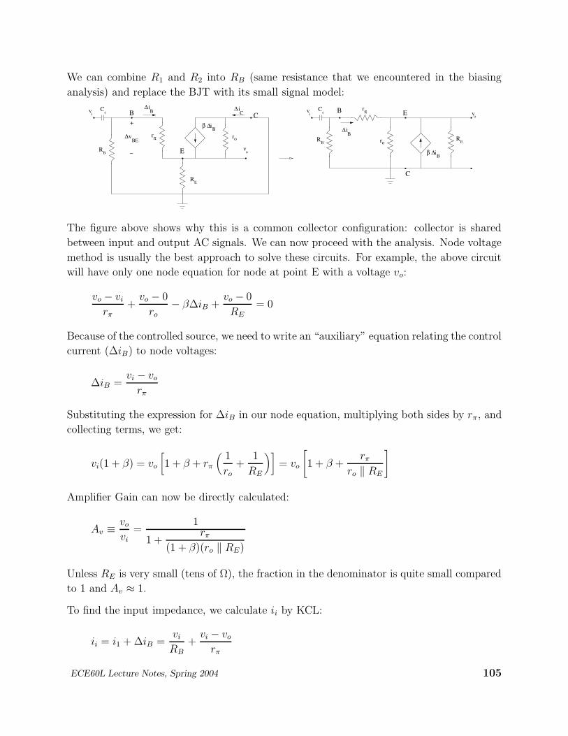
We can combine R1 and R2 into RB (same resistance that we encountered in the biasing
analysis) and replace the BJT with its small signal model:
vi
RB
RE
i∆B
ovv
ii∆C
i∆B
vo
RE
Cc
∆BE
v
Cc
rπ
rπ
ro ro
β ∆B
β ∆B
B
C
E
RB
C+
_
B
E
i
i
The figure above shows why this is a common collector configuration: collector is shared
between input and output AC signals. We can now proceed with the analysis. Node voltage
method is usually the best approach to solve these circuits. For example, the above circuit
will have only one node equation for node at point E with a voltage vo:
vo − vi
rπ
+vo − 0
ro
− β∆iB +vo − 0
RE
= 0
Because of the controlled source, we need to write an “auxiliary” equation relating the control
current (∆iB) to node voltages:
∆iB =vi − vo
rπ
Substituting the expression for ∆iB in our node equation, multiplying both sides by rπ, and
collecting terms, we get:
vi(1 + β) = vo
[
1 + β + rπ
(
1
ro
+1
RE
)]
= vo
[
1 + β +rπ
ro ‖ RE
]
Amplifier Gain can now be directly calculated:
Av ≡ vo
vi
=1
1 +rπ
(1 + β)(ro ‖ RE)
Unless RE is very small (tens of Ω), the fraction in the denominator is quite small compared
to 1 and Av ≈ 1.
To find the input impedance, we calculate ii by KCL:
ii = i1 + ∆iB =vi
RB
+vi − vo
rπ
ECE60L Lecture Notes, Spring 2004 105
Since vo ≈ vi, we have ii = vi/RB or
Ri ≡vi
ii= RB
Note that RB is the combination of our biasing resistors R1 and R2. With alternative biasing
schemes which do not require R1 and R2, (and, therefore RB → ∞), the input resistance of
the emitter follower circuit will become large. In this case, we cannot use vo ≈ vi. Using the
full expression for vo from above, the input resistance of the emitter follower circuit becomes:
Ri ≡vi
ii= RB ‖ [rπ + (RE ‖ ro)(1 + β)]
and it is quite large (hundreds of kΩ to several MΩ) for RB → ∞. Such a circuit is in fact
the first stage of the 741 OpAmp.
The output resistance of the common collector amplifier (in fact for all transistor amplifiers)
is somewhat complicated because the load can be configured in two ways (see figure): First,
RE, itself, is the load. This is the case when the common collector is used as a “current
amplifier” to raise the power level and to drive the load. The output resistance of the circuit
is Ro as is shown in the circuit model. This is usually the case when values of Ro and Ai
(current gain) is quoted in electronic text books.
R2
VCC
vi
vo
RL
R1
Cc
E
=RE
R is the Load
RE
R2
VCC
vi
vo
R1
Cc
RL
Separate Load
vi
RB
i∆B
ov
RE
Ro
Cc B
C
Eπr
ro
β∆ Bi
vi
RB
i∆B
Cc
RE
oR’
B
C
Eπr
ro
β∆ B
ov
RL
i
Alternatively, the load can be placed in parallel to RE. This is done when the common
collector amplifier is used as a buffer (Av ≈ 1, Ri large). In this case, the output resistance
is denoted by R′
o (see figure). For this circuit, BJT sees a resistance of RE ‖ RL. Obviously,
if we want the load not to affect the emitter follower circuit, we should use RL to be much
ECE60L Lecture Notes, Spring 2004 106
larger than RE. In this case, little current flows in RL which is fine because we are using
this configuration as a buffer and not to amplify the current and power. As such, value of
R′
o or Ai does not have much use.
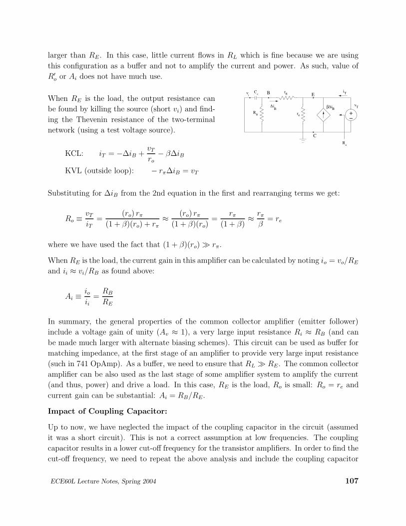
vi
RB
i∆B
Ro
iT
vT
Cc B
C
Erπ
or
β∆ Bi
+−
When RE is the load, the output resistance can
be found by killing the source (short vi) and find-
ing the Thevenin resistance of the two-terminal
network (using a test voltage source).
KCL: iT = −∆iB +vT
ro
− β∆iB
KVL (outside loop): − rπ∆iB = vT
Substituting for ∆iB from the 2nd equation in the first and rearranging terms we get:
Ro ≡vT
iT=
(ro) rπ
(1 + β)(ro) + rπ
≈ (ro) rπ
(1 + β)(ro)=
rπ
(1 + β)≈ rπ
β= re
where we have used the fact that (1 + β)(ro) rπ.
When RE is the load, the current gain in this amplifier can be calculated by noting io = vo/RE
and ii ≈ vi/RB as found above:
Ai ≡ioii
=RB
RE
In summary, the general properties of the common collector amplifier (emitter follower)
include a voltage gain of unity (Av ≈ 1), a very large input resistance Ri ≈ RB (and can
be made much larger with alternate biasing schemes). This circuit can be used as buffer for
matching impedance, at the first stage of an amplifier to provide very large input resistance
(such in 741 OpAmp). As a buffer, we need to ensure that RL RE. The common collector
amplifier can be also used as the last stage of some amplifier system to amplify the current
(and thus, power) and drive a load. In this case, RE is the load, Ro is small: Ro = re and
current gain can be substantial: Ai = RB/RE.
Impact of Coupling Capacitor:
Up to now, we have neglected the impact of the coupling capacitor in the circuit (assumed
it was a short circuit). This is not a correct assumption at low frequencies. The coupling
capacitor results in a lower cut-off frequency for the transistor amplifiers. In order to find the
cut-off frequency, we need to repeat the above analysis and include the coupling capacitor
ECE60L Lecture Notes, Spring 2004 107
impedance in the calculation. In most cases, however, the impact of the coupling capacitor
and the lower cut-off frequency can be deduced be examining the amplifier circuit model.
+− V L
oI
o
+
−
i
i
+
−
o
AVi
i
V’
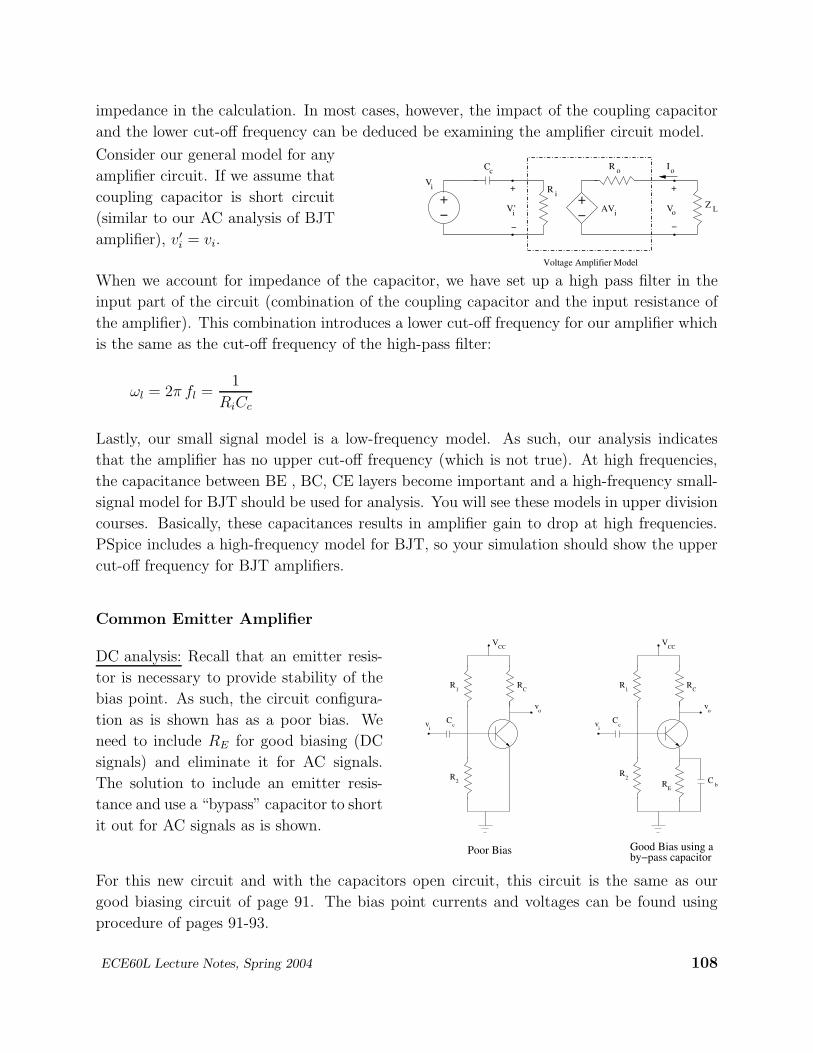
c
Voltage Amplifier Model
C
Z
R+−
V
RConsider our general model for any
amplifier circuit. If we assume that
coupling capacitor is short circuit
(similar to our AC analysis of BJT
amplifier), v′
i = vi.
When we account for impedance of the capacitor, we have set up a high pass filter in the
input part of the circuit (combination of the coupling capacitor and the input resistance of
the amplifier). This combination introduces a lower cut-off frequency for our amplifier which
is the same as the cut-off frequency of the high-pass filter:
ωl = 2π fl =1
RiCc
Lastly, our small signal model is a low-frequency model. As such, our analysis indicates
that the amplifier has no upper cut-off frequency (which is not true). At high frequencies,
the capacitance between BE , BC, CE layers become important and a high-frequency small-
signal model for BJT should be used for analysis. You will see these models in upper division
courses. Basically, these capacitances results in amplifier gain to drop at high frequencies.
PSpice includes a high-frequency model for BJT, so your simulation should show the upper
cut-off frequency for BJT amplifiers.
Common Emitter Amplifier
RC
VCC
R1
vo
vi
Cc
R2
RC
VCC
R1
vo
vi
Cc
CbR
E
R2
Good Bias using aby−pass capacitor
Poor Bias
DC analysis: Recall that an emitter resis-
tor is necessary to provide stability of the
bias point. As such, the circuit configura-
tion as is shown has as a poor bias. We
need to include RE for good biasing (DC
signals) and eliminate it for AC signals.
The solution to include an emitter resis-
tance and use a “bypass” capacitor to short
it out for AC signals as is shown.
For this new circuit and with the capacitors open circuit, this circuit is the same as our
good biasing circuit of page 91. The bias point currents and voltages can be found using
procedure of pages 91-93.
ECE60L Lecture Notes, Spring 2004 108
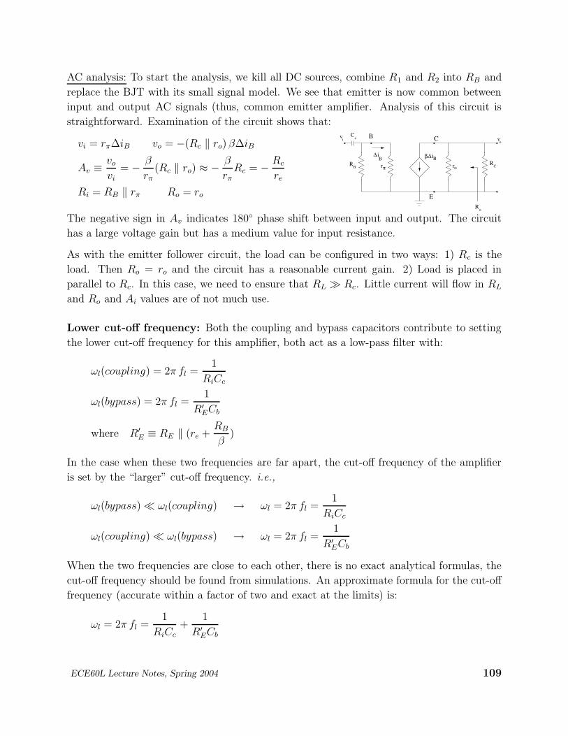
AC analysis: To start the analysis, we kill all DC sources, combine R1 and R2 into RB and
replace the BJT with its small signal model. We see that emitter is now common between
input and output AC signals (thus, common emitter amplifier. Analysis of this circuit is
straightforward. Examination of the circuit shows that:v
i
RB
i∆B
ov
Ro
RC
Cc B
E
C
rπ
β∆ B
or
i
vi = rπ∆iB vo = −(Rc ‖ ro) β∆iB
Av ≡ vo
vi
= − β
rπ
(Rc ‖ ro) ≈ − β
rπ
Rc = − Rc
re
Ri = RB ‖ rπ Ro = ro
The negative sign in Av indicates 180 phase shift between input and output. The circuit
has a large voltage gain but has a medium value for input resistance.
As with the emitter follower circuit, the load can be configured in two ways: 1) Rc is the
load. Then Ro = ro and the circuit has a reasonable current gain. 2) Load is placed in
parallel to Rc. In this case, we need to ensure that RL Rc. Little current will flow in RL
and Ro and Ai values are of not much use.
Lower cut-off frequency: Both the coupling and bypass capacitors contribute to setting
the lower cut-off frequency for this amplifier, both act as a low-pass filter with:
ωl(coupling) = 2π fl =1
RiCc
ωl(bypass) = 2π fl =1
R′
ECb
where R′
E ≡ RE ‖ (re +RB
β)
In the case when these two frequencies are far apart, the cut-off frequency of the amplifier
is set by the “larger” cut-off frequency. i.e.,
ωl(bypass) ωl(coupling) → ωl = 2π fl =1
RiCc
ωl(coupling) ωl(bypass) → ωl = 2π fl =1
R′
ECb
When the two frequencies are close to each other, there is no exact analytical formulas, the
cut-off frequency should be found from simulations. An approximate formula for the cut-off
frequency (accurate within a factor of two and exact at the limits) is:
ωl = 2π fl =1
RiCc
+1
R′
ECb
ECE60L Lecture Notes, Spring 2004 109
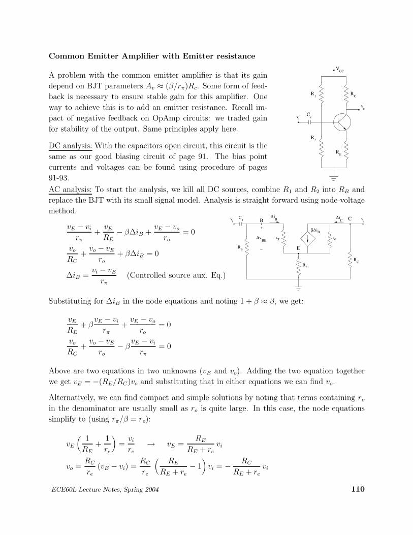
Common Emitter Amplifier with Emitter resistance
C
VCC
R1
R2
ER
cC
vo
vi
R
A problem with the common emitter amplifier is that its gain
depend on BJT parameters Av ≈ (β/rπ)Rc. Some form of feed-
back is necessary to ensure stable gain for this amplifier. One
way to achieve this is to add an emitter resistance. Recall im-
pact of negative feedback on OpAmp circuits: we traded gain
for stability of the output. Same principles apply here.
DC analysis: With the capacitors open circuit, this circuit is the
same as our good biasing circuit of page 91. The bias point
currents and voltages can be found using procedure of pages
91-93.
AC analysis: To start the analysis, we kill all DC sources, combine R1 and R2 into RB and
replace the BJT with its small signal model. Analysis is straight forward using node-voltage
method.1
Cvi
i∆C
i∆B v
o
∆BE
v
RE
RC
RB
+
_
B
E
C
πr
β∆ B
ro
ivE − vi
rπ
+vE
RE
− β∆iB +vE − vo
ro
= 0
vo
RC
+vo − vE
ro
+ β∆iB = 0
∆iB =vi − vE
rπ
(Controlled source aux. Eq.)
Substituting for ∆iB in the node equations and noting 1 + β ≈ β, we get:
vE
RE
+ βvE − vi
rπ
+vE − vo
ro
= 0
vo
RC
+vo − vE
ro
− βvE − vi
rπ
= 0
Above are two equations in two unknowns (vE and vo). Adding the two equation together
we get vE = −(RE/RC)vo and substituting that in either equations we can find vo.
Alternatively, we can find compact and simple solutions by noting that terms containing ro
in the denominator are usually small as ro is quite large. In this case, the node equations
simplify to (using rπ/β = re):
vE
(
1
RE
+1
re
)
=vi
re
→ vE =RE
RE + re
vi
vo =RC
re
(vE − vi) =RC
re
(
RE
RE + re
− 1)
vi = − RC
RE + re
vi
ECE60L Lecture Notes, Spring 2004 110
Then, the voltage gain and input resistance can be easily calculated from the above equations:
Av =vo
vi
= − RC
RE + re
≈ − RC
RE
Ri = RB ‖ [β(RE + re)]
As before the minus sign in Av indicates a 180 phase shift between input and output signals.
Note the impact of negative feedback introduced by the emitter resistance. The voltage gain
is independent of BJT parameters and is set by RC and RE as RE re (recall OpAmp
inverting amplifier!). The input resistance is increased dramatically.
To find Ro, we need to follow the procedure similar to that of page 107 to get:
Ro = ro ×
1
rπ
+1
RE
+β
rπ
+1
ro
1
rπ
+1
RE
Assuming RE ro and RE rπ, the above equation simplifies to:
Ro ≈ ro
(
RE
re
+ 1)
Lower cut-off frequency: The coupling capacitor together with the input resistance of
the amplifer lead to a lower cut-off freqnecy for this amplifer (similar to emitter follower).
The lower cut-off freqncy is geivn by:
ωl = 2π fl =1
RiCc
ECE60L Lecture Notes, Spring 2004 111
C
VCC
R1
R2
vo
vi
Cc
Cb
RE1
R
RE2
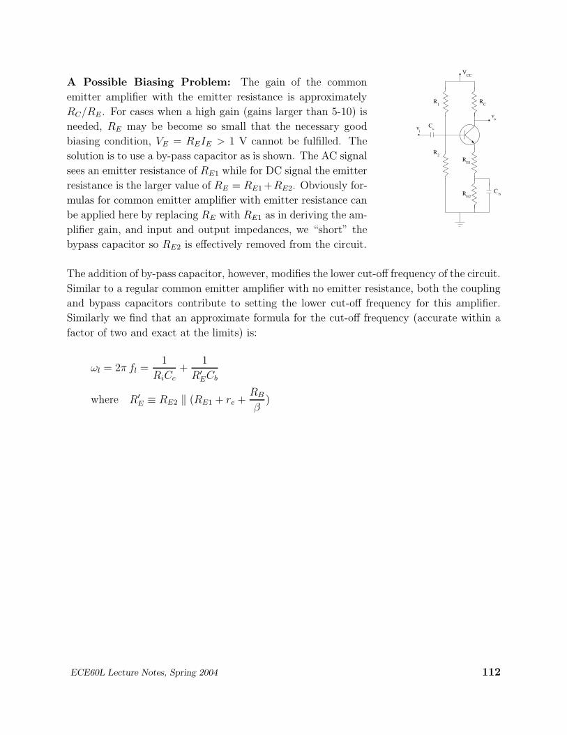
A Possible Biasing Problem: The gain of the common
emitter amplifier with the emitter resistance is approximately
RC/RE. For cases when a high gain (gains larger than 5-10) is
needed, RE may be become so small that the necessary good
biasing condition, VE = REIE > 1 V cannot be fulfilled. The
solution is to use a by-pass capacitor as is shown. The AC signal
sees an emitter resistance of RE1 while for DC signal the emitter
resistance is the larger value of RE = RE1 +RE2. Obviously for-
mulas for common emitter amplifier with emitter resistance can
be applied here by replacing RE with RE1 as in deriving the am-
plifier gain, and input and output impedances, we “short” the
bypass capacitor so RE2 is effectively removed from the circuit.
The addition of by-pass capacitor, however, modifies the lower cut-off frequency of the circuit.
Similar to a regular common emitter amplifier with no emitter resistance, both the coupling
and bypass capacitors contribute to setting the lower cut-off frequency for this amplifier.
Similarly we find that an approximate formula for the cut-off frequency (accurate within a
factor of two and exact at the limits) is:
ωl = 2π fl =1
RiCc
+1
R′
ECb
where R′
E ≡ RE2 ‖ (RE1 + re +RB
β)
ECE60L Lecture Notes, Spring 2004 112
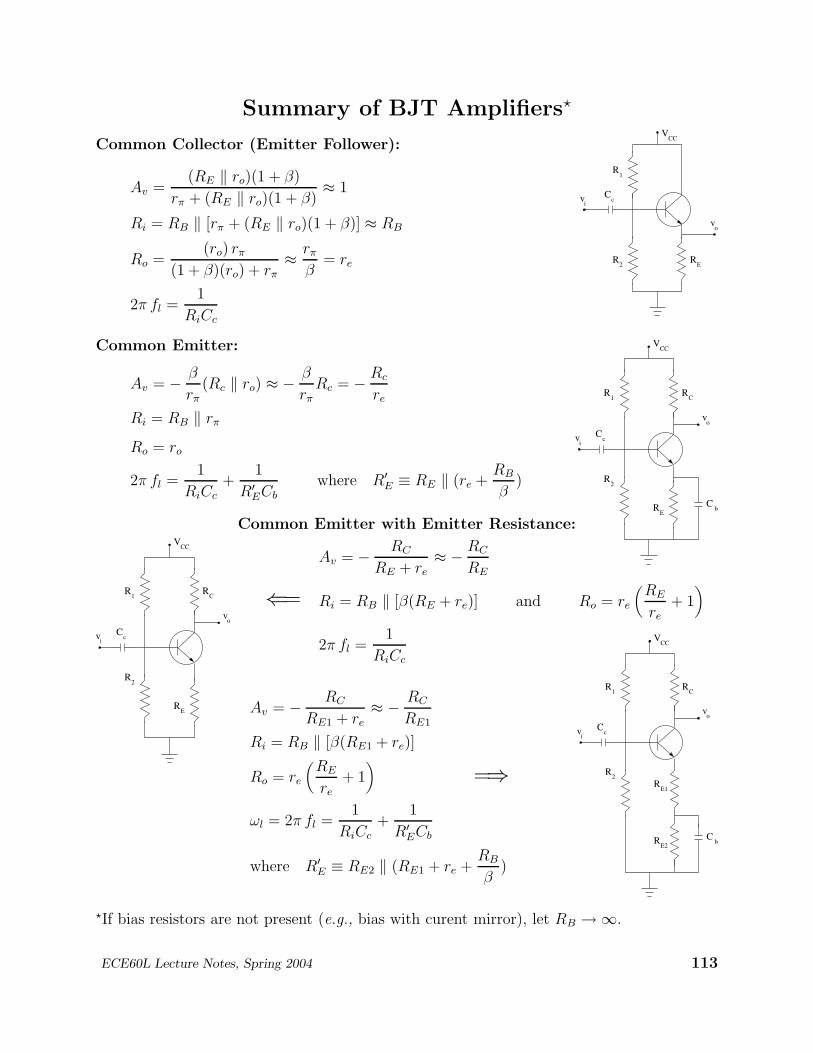
Summary of BJT Amplifiers?
RE
R2
VCC
vi
vo
R1
cC
Common Collector (Emitter Follower):
Av =(RE ‖ ro)(1 + β)
rπ + (RE ‖ ro)(1 + β)≈ 1
Ri = RB ‖ [rπ + (RE ‖ ro)(1 + β)] ≈ RB
Ro =(ro) rπ
(1 + β)(ro) + rπ
≈ rπ
β= re
2π fl =1
RiCc
C
VCC
R1
R2
vo
vi
Cc
Cb
R
RE
Common Emitter:
Av = − β
rπ
(Rc ‖ ro) ≈ − β
rπ
Rc = − Rc
re
Ri = RB ‖ rπ
Ro = ro
2π fl =1
RiCc
+1
R′
ECb
where R′
E ≡ RE ‖ (re +RB
β)
Common Emitter with Emitter Resistance:
C
VCC
R1
R2
ER
cC
vo
vi
R ⇐=
Av = − RC
RE + re
≈ − RC
RE
Ri = RB ‖ [β(RE + re)] and Ro = re
(
RE
re
+ 1)
2π fl =1
RiCc
C
VCC
R1
R2
vo
vi
Cc
Cb
RE1
R
RE2
Av = − RC
RE1 + re
≈ − RC
RE1
Ri = RB ‖ [β(RE1 + re)]
Ro = re
(
RE
re
+ 1)
=⇒
ωl = 2π fl =1
RiCc
+1
R′
ECb
where R′
E ≡ RE2 ‖ (RE1 + re +RB
β)
?If bias resistors are not present (e.g., bias with curent mirror), let RB → ∞.
ECE60L Lecture Notes, Spring 2004 113
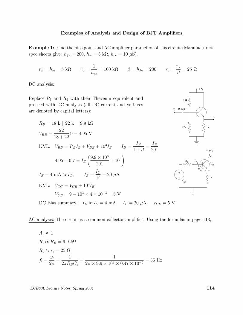
Examples of Analysis and Design of BJT Amplifiers
Example 1: Find the bias point and AC amplifier parameters of this circuit (Manufacturers’
spec sheets give: hfe = 200, hie = 5 kΩ, hoe = 10 µS).
rπ = hie = 5 kΩ ro =1
hoe
= 100 kΩ β = hfe = 200 re =rπ
β= 25 Ω
DC analysis:
vi
vo
0.47 Fµ
9 V
18k
22k 1k
VBB
IB
BEV
CEV
CI
RB+
_+
_+−
9 V
1k
Replace R1 and R2 with their Thevenin equivalent and
proceed with DC analysis (all DC current and voltages
are denoted by capital letters):
RB = 18 k ‖ 22 k = 9.9 kΩ
VBB =22
18 + 229 = 4.95 V
KVL: VBB = RBIB + VBE + 103IE IB =IE
1 + β=
IE
201
4.95 − 0.7 = IE
(
9.9 × 10³
201+ 103
)
IE = 4 mA ≈ IC , IB =IC
β= 20 µA
KVL: VCC = VCE + 103IE
VCE = 9 − 103 × 4 × 10−3 = 5 V
DC Bias summary: IE ≈ IC = 4 mA, IB = 20 µA, VCE = 5 V
AC analysis: The circuit is a common collector amplifier. Using the formulas in page 113,
Av ≈ 1
Ri ≈ RB = 9.9 kΩ
Ro ≈ re = 25 Ω
fl =ωl
2π=
1
2πRBCc
=1
2π × 9.9 × 103 × 0.47 × 10−6= 36 Hz
ECE60L Lecture Notes, Spring 2004 114
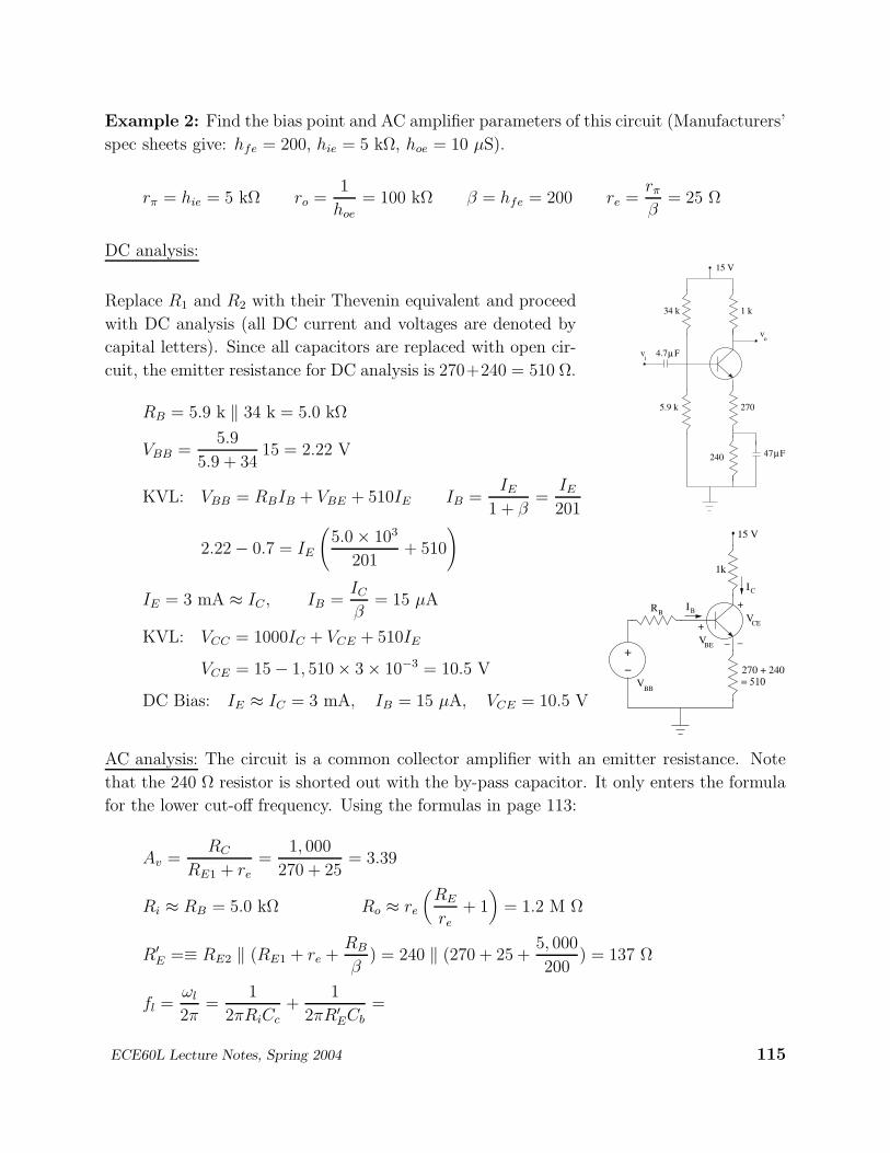
Example 2: Find the bias point and AC amplifier parameters of this circuit (Manufacturers’
spec sheets give: hfe = 200, hie = 5 kΩ, hoe = 10 µS).
rπ = hie = 5 kΩ ro =1
hoe
= 100 kΩ β = hfe = 200 re =rπ
β= 25 Ω
DC analysis:
vo
vi µ4.7 F
47 Fµ
15 V
34 k 1 k
2705.9 k
240
VBB
IB
BEV
CEVRB
CI
+
_+
_+−
= 510270 + 240
1k
15 V
Replace R1 and R2 with their Thevenin equivalent and proceed
with DC analysis (all DC current and voltages are denoted by
capital letters). Since all capacitors are replaced with open cir-
cuit, the emitter resistance for DC analysis is 270+240 = 510 Ω.
RB = 5.9 k ‖ 34 k = 5.0 kΩ
VBB =5.9
5.9 + 3415 = 2.22 V
KVL: VBB = RBIB + VBE + 510IE IB =IE
1 + β=
IE
201
2.22 − 0.7 = IE
(
5.0 × 10³
201+ 510
)
IE = 3 mA ≈ IC , IB =IC
β= 15 µA
KVL: VCC = 1000IC + VCE + 510IE
VCE = 15 − 1, 510 × 3 × 10−3 = 10.5 V
DC Bias: IE ≈ IC = 3 mA, IB = 15 µA, VCE = 10.5 V
AC analysis: The circuit is a common collector amplifier with an emitter resistance. Note
that the 240 Ω resistor is shorted out with the by-pass capacitor. It only enters the formula
for the lower cut-off frequency. Using the formulas in page 113:
Av =RC
RE1 + re
=1, 000
270 + 25= 3.39
Ri ≈ RB = 5.0 kΩ Ro ≈ re
(
RE
re
+ 1)
= 1.2 M Ω
R′
E =≡ RE2 ‖ (RE1 + re +RB
β) = 240 ‖ (270 + 25 +
5, 000
200) = 137 Ω
fl =ωl
2π=
1
2πRiCc
+1
2πR′
ECb
=
ECE60L Lecture Notes, Spring 2004 115
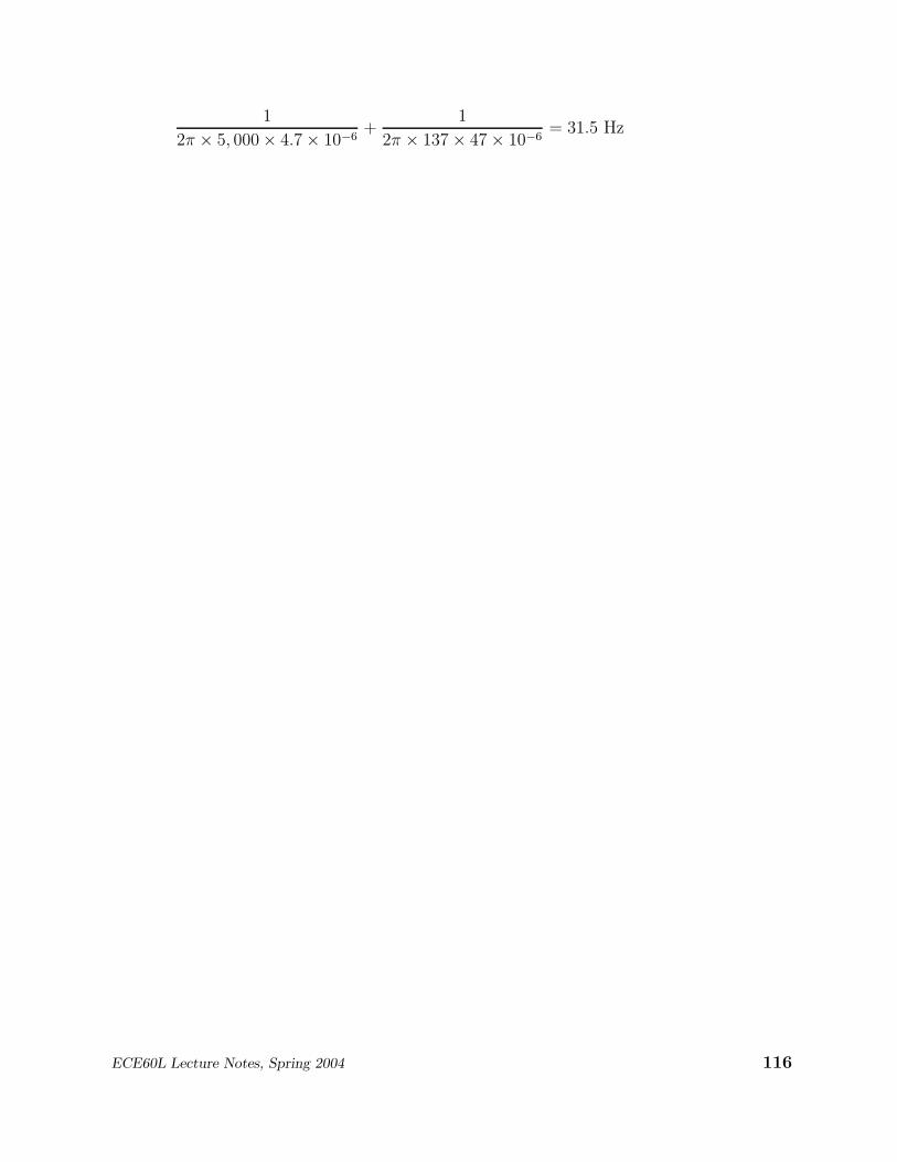
1
2π × 5, 000 × 4.7 × 10−6+
1
2π × 137 × 47 × 10−6= 31.5 Hz
ECE60L Lecture Notes, Spring 2004 116
Example 3: Design a BJT amplifier with a gain of 4 and a lower cut-off frequency of 100 Hz.
The Q point parameters should be IC = 3 mA and VCE = 7.5 V. (Manufacturers’ spec sheets
give: βmin = 100, β = 200, hie = 5 kΩ, hoe = 10 µS).
C
VCC
R1
R2
ER
cC
vo
vi
R
vCE
i C
i B
vBE
RC
RE
VCC
VBB
RB
+
_+
_+−
rπ = hie = 5 kΩ ro =1
hoe
= 100 kΩ re =rπ
β= 25 Ω
The prototype of this circuit is a common emitter amplifier with
an emitter resistance. Using formulas of page 113 (re = rπ/hfe =
25 Ω),
|Av| =RC
RE + re
≈ RC
RE
= 4
The lower cut-off frequency will set the value of Cc.
We start with the DC bias: As VCC is not given, we need to
choose it. To set the Q-point in the middle of load line, set
VCC = 2VCE = 15 V. Then, noting IC ≈ IE,:
VCC = RCIC + VCE + REIE
15 − 7.5 = 3 × 10⁻³(RC + RE) → RC + RE = 2.5 kΩ
Values of RC and RE can be found from the above equation
together with the AC gain of the amplifier, AV = 4. Ignoring re
compared to RE (usually a good approximation), we get:
RC
RE
= 4 → 4RE + RE = 2.5 kΩ → RE = 500 Ω, RC = 2. kΩ
Commercial values are RE = 510 Ω and RC = 2 kΩ. Use these commercial values for the
rest of analysis.
We need to check if VE > 1 V, the condition for good biasing. VE = REIE = 510×3×10−3 =
1.5 > 1, it is OK (See next example for the case when VE is smaller than 1 V).
We now proceed to find RB and VBB . RB is found from good bias condition and VBB from
a KVL in BE loop:
RB (β + 1)RE → RB = 0.1(βmin + 1)RE = 0.1 × 101 × 510 = 5.1 kΩ
KVL: VBB = RBIB + VBE + REIE
VBB = 5.1 × 1033 × 10−3
201+ 0.7 + 510 × 3 × 10−3 = 2.28 V
ECE60L Lecture Notes, Spring 2004 117
Bias resistors R1 and R2 are now found from RB and VBB :
RB = R1 ‖ R2 =R1R2
R1 + R2
= 5 kΩ
VBB
VCC
=R2
R1 + R2
=2.28
15= 0.152
R1 can be found by dividing the two equations: R1 = 33 kΩ. R2 is found from the equation
for VBB to be R2 = 5.9 kΩ. Commercial values are R1 = 33 kΩ and R2 = 6.2 kΩ.
Lastly, we have to find the value of the coupling capacitor:
ωl =1
RiCc
= 2π × 100
Using Ri ≈ RB = 5.1 kΩ, we find Cc = 3 × 10⁻⁷ F or a commercial values of Cc = 300 nF.
So, are design values are: R1 = 33 kΩ, R2 = 6.2 kΩ, RE = 510 Ω, RC = 2 kΩ. and
Cc = 300 nF.
Example 4: Design a BJT amplifier with a gain of 10 and a lower cut-off frequency of
100 Hz. The Q point parameters should be IC = 3 mA and VCE = 7.5 V. A power supply
of 15 V is available. Manufacturers’ spec sheets give: βmin = 100, hfe = 200, rπ = 5 kΩ,
hoe = 10 µS.
C
VCC
R1
R2
ER
cC
vo
vi
Rrπ = hie = 5 kΩ ro =
1
hoe
= 100 kΩ re =rπ
β= 25 Ω
The prototype of this circuit is a common emitter amplifier with an
emitter resistance. Using formulas of page 113:
|Av| =RC
RE + re
≈ RC
RE
= 10
The lower cut-off frequency will set the value of Cc.
We start with the DC bias: As the power supply voltage is given, we set VCC = 15 V. Then,
noting IC ≈ IE,:
VCC = RCIC + VCE + REIE
15 − 7.5 = 3 × 10⁻³(RC + RE) → RC + RE = 2.5 kΩ
ECE60L Lecture Notes, Spring 2004 118
Values of RC and RE can be found from the above equation together with the AC gain of
the amplifier AV = 10. Ignoring re compared to RE (usually a good approximation), we get:
RC
RE
= 10 → 10RE + RE = 2.5 kΩ → RE = 227 Ω, RC = 2.27 kΩ
C
VCC
R1
R2
vo
vi
Cc
Cb
RE1
R
RE2
vCE
i C
i B
vBE
RC
VCC
VBB
RB
RE1 R
E2
+
_+
_+− +
We need to check if VE > 1 V which is the condition for good
biasing: VE = REIE = 227 × 3 × 10−3 = 0.69 < 1. Therefore,
we need to use a bypass capacitor and modify our circuits as is
shown.
For DC analysis, the emitter resistance is RE1 + RE2 while for
AC analysis, the emitter resistance will be RE1. Therefore:
DC Bias: RC + RE1 + RE2 = 2.5 kΩ
AC gain: Av =RC
RE1
= 10
Above are two equations in three unknowns. A third equation is
derived by setting VE = 1 V to minimize the value of RE1 +RE2.
VE = (RE1 + RE2)IE
RE1 + RE2 =1
3 × 10−3= 333
Now, solving for RC , RE1, and RE2, we find RC = 2.2 kΩ,
RE1 = 220 Ω, and RE2 = 110 Ω (All commercial values).
We can now proceed to find RB and VBB :
RB (β + 1)(RE1 + RE2)
RB = 0.1(βmin + 1)(RE1 + RE2) = 0.1 × 101 × 330 = 3.3 kΩ
KVL: VBB = RBIB + VBE + REIE
VBB = 3.3 × 1033 × 10−3
201+ 0.7 + 330 × 3 × 10−3 = 1.7 V
Bias resistors R1 and R2 are now found from RB and VBB:
RB = R1 ‖ R2 =R1R2
R1 + R2
= 3.3 kΩ
VBB
VCC
=R2
R1 + R2
=1
15= 0.066
ECE60L Lecture Notes, Spring 2004 119
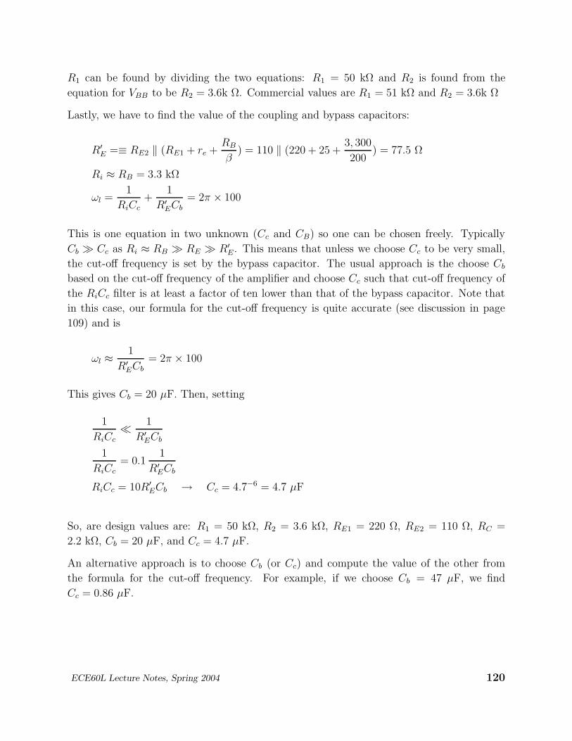
R1 can be found by dividing the two equations: R1 = 50 kΩ and R2 is found from the
equation for VBB to be R2 = 3.6k Ω. Commercial values are R1 = 51 kΩ and R2 = 3.6k Ω
Lastly, we have to find the value of the coupling and bypass capacitors:
R′
E =≡ RE2 ‖ (RE1 + re +RB
β) = 110 ‖ (220 + 25 +
3, 300
200) = 77.5 Ω
Ri ≈ RB = 3.3 kΩ
ωl =1
RiCc
+1
R′
ECb
= 2π × 100
This is one equation in two unknown (Cc and CB) so one can be chosen freely. Typically
Cb Cc as Ri ≈ RB RE R′
E. This means that unless we choose Cc to be very small,
the cut-off frequency is set by the bypass capacitor. The usual approach is the choose Cb
based on the cut-off frequency of the amplifier and choose Cc such that cut-off frequency of
the RiCc filter is at least a factor of ten lower than that of the bypass capacitor. Note that
in this case, our formula for the cut-off frequency is quite accurate (see discussion in page
109) and is
ωl ≈1
R′
ECb
= 2π × 100
This gives Cb = 20 µF. Then, setting
1
RiCc
1
R′
ECb
1
RiCc
= 0.11
R′
ECb
RiCc = 10R′
ECb → Cc = 4.7−6 = 4.7 µF
So, are design values are: R1 = 50 kΩ, R2 = 3.6 kΩ, RE1 = 220 Ω, RE2 = 110 Ω, RC =
2.2 kΩ, Cb = 20 µF, and Cc = 4.7 µF.
An alternative approach is to choose Cb (or Cc) and compute the value of the other from
the formula for the cut-off frequency. For example, if we choose Cb = 47 µF, we find
Cc = 0.86 µF.
ECE60L Lecture Notes, Spring 2004 120
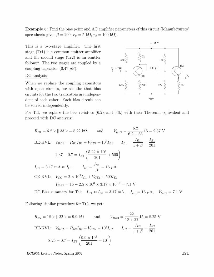
Example 5: Find the bias point and AC amplifier parameters of this circuit (Manufacturers’
spec sheets give: β = 200, rπ = 5 kΩ, ro = 100 kΩ).
vi
vo
33k 18k
22k 1k
15 V
6.2k 500
2k
µµTr2
Tr1
0.47 F4.7 F
This is a two-stage amplifier. The first
stage (Tr1) is a common emitter amplifier
and the second stage (Tr2) is an emitter
follower. The two stages are coupled by a
coupling capacitor (0.47 µF).
DC analysis:
When we replace the coupling capacitors
with open circuits, we see the that bias
circuits for the two transistors are indepen-
dent of each other. Each bias circuit can
be solved independently.
For Tr1, we replace the bias resistors (6.2k and 33k) with their Thevenin equivalent and
proceed with DC analysis:
RB1 = 6.2 k ‖ 33 k = 5.22 kΩ and VBB1 =6.2
6.2 + 3315 = 2.37 V
BE-KVL: VBB1 = RB1IB1 + VBE1 + 103IE1 IB1 =IE1
1 + β=
IE1
201
2.37 − 0.7 = IE1
(
5.22 × 10³
201+ 500
)
IE1 = 3.17 mA ≈ IC1, IB1 =IC1
β= 16 µA
CE-KVL: VCC = 2 × 10³IC1 + VCE1 + 500IE1
VCE1 = 15 − 2.5 × 103 × 3.17 × 10−3 = 7.1 V
DC Bias summary for Tr1: IE1 ≈ IC1 = 3.17 mA, IB1 = 16 µA, VCE1 = 7.1 V
Following similar procedure for Tr2, we get:
RB2 = 18 k ‖ 22 k = 9.9 kΩ and VBB2 =22
18 + 2215 = 8.25 V
BE-KVL: VBB2 = RB2IB2 + VBE2 + 103IE2 IB2 =IE2
1 + β=
IE2
201
8.25 − 0.7 = IE2
(
9.9 × 10³
201+ 103
)
ECE60L Lecture Notes, Spring 2004 121
IE2 = 7.2 mA ≈ IC2, IB2 =IC2
β= 36 µA
CE-KVL: VCC = VCE2 + 103IE2
VCE2 = 15 − 103 × 7.2 × 10−3 = 7.8 V
DC Bias summary for TR2: IE2 ≈ IC2 = 7.2 mA, IB2 = 36 µA, VCE2 = 7.8 V
AC analysis:
We start with the emitter follower circuit (Tr2) as the input resistance of this circuit will
appear as the load for the common emitter amplifier (Tr1). Using the formulas in page 113:
Av2 ≈ 1
Ri2 ≈ RB2 = 9.9 kΩ
fl2 =ωl2
2π=
1
2πRB2Cc2
=1
2π × 9.9 × 103 × 0.47 × 10−6= 34 Hz
Since Ri2 = 9.9 kΩ is NOT much larger than the collector resistor of common emitter
amplifier (Tr1), it will affect the first circuit. Following discussion in pages 106 and 111, the
effect of this load can be taken into by replacing RC in common emitter amplifiers formulas
with R′
C = RC ‖ RL = RC1 ‖ Ri2 = 2 k ‖ 9.9 kΩ = 1.66 kΩ.
|Av1| ≈R′
C
RE
=1.66k
500= 3.3
Ri1 ≈ RB1 = 5.22 kΩ
fl1 =ωl1
2π=
1
2πRB1Cc1
=1
2π × 5.22 × 103 × 4.7 × 10−6= 6.5 Hz
The overall gain of the two-stage amplifier is then Av = Av1×Av2 = 3.3. The input resistance
of the two-stage amplifier is the input resistance of the first-stage (Tr1), Ri = 9.9 kΩ. To
find the lower cut-off frequency of the two-stage amplifier, we note that:
Av1(jω) =Av1
1 − jωl1/ωand Av2(jω) =
Av2
1 − jωl2/ω
Av(jω) = Av1(jω) × Av2(jω) =Av1Av2
(1 − jωl1/ω)(1− jωl2/ω)
From above, it is clear that the maximum value of Av(jω) is Av1Av2 and the cut-off frequency,
ωl can be found from —Av(jω = ωl)| = Av1Av2/√
2 (similar to procedure we used for filters).
For the circuit above, since ωl2 ωl1 the lower cut-off frequency would be very close to ωl2.
So, the lower-cut-off frequency of this amplifier is 34 Hz.
ECE60L Lecture Notes, Spring 2004 122
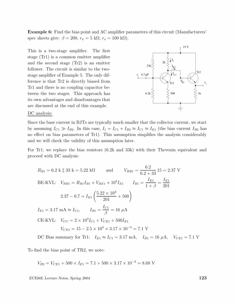
Example 6: Find the bias point and AC amplifier parameters of this circuit (Manufacturers’
spec sheets give: β = 200, rπ = 5 kΩ, ro = 100 kΩ).
vi
vo
33k
15 V
6.2k 500
µ
Tr1
4.7 F
1k
Tr2
IB2
I
I12k
C1
VB2
This is a two-stage amplifier. The first
stage (Tr1) is a common emitter amplifier
and the second stage (Tr2) is an emitter
follower. The circuit is similar to the two-
stage amplifier of Example 5. The only dif-
ference is that Tr2 is directly biased from
Tr1 and there is no coupling capacitor be-
tween the two stages. This approach has
its own advantages and disadvantages that
are discussed at the end of this example.
DC analysis:
Since the base current in BJTs are typically much smaller that the collector current, we start
by assuming IC1 IB2. In this case, I1 = IC1 + IB2 ≈ IC1 ≈ IE1 (the bias current IB2 has
no effect on bias parameters of Tr1). This assumption simplifies the analysis considerably
and we will check the validity of this assumption later.
For Tr1, we replace the bias resistors (6.2k and 33k) with their Thevenin equivalent and
proceed with DC analysis:
RB1 = 6.2 k ‖ 33 k = 5.22 kΩ and VBB1 =6.2
6.2 + 3315 = 2.37 V
BE-KVL: VBB1 = RB1IB1 + VBE1 + 103IE1 IB1 =IE1
1 + β=
IE1
201
2.37 − 0.7 = IE1
(
5.22 × 10³
201+ 500
)
IE1 = 3.17 mA ≈ IC1, IB1 =IC1
β= 16 µA
CE-KVL: VCC = 2 × 10³IC1 + VCE1 + 500IE1
VCE1 = 15 − 2.5 × 103 × 3.17 × 10−3 = 7.1 V
DC Bias summary for Tr1: IE1 ≈ IC1 = 3.17 mA, IB1 = 16 µA, VCE1 = 7.1 V
To find the bias point of TR2, we note:
VB2 = VCE1 + 500 × IE1 = 7.1 + 500 × 3.17 × 10−3 = 8.68 V
ECE60L Lecture Notes, Spring 2004 123
BE-KVL: VB2 = VBE2 + 103IE2
8.68 − 0.7 = 103IE2
IE2 = 8.0 mA ≈ IC2, IB2 =IC2
β= 40 µA
KVL: VCC = VCE2 + 103IE2
VCE2 = 15 − 103 × 8.0 × 10−3 = 7.0 V
DC Bias summary for TR2: IE2 ≈ IC2 = 8.0 mA, IB2 = 40 µA, VCE2 = 7.0 V
We now check our assumption of IC1 IB2. We find IC1 = 3.17 mA IB2 = 41 µA. So,
our assumption was justified.
It should be noted that this bias arrangement is also stable to variation in transistor β. The
bias resistors in the first stage will ensure that IC1 (≈ IE1) and VCE1 is stable to variation
of TR1 β. Since VB2 = VCE1 + RE1 × IE1, VB2 will also be stable to variation in transistor
β. Finally, VB2 = VBE2 + RE2IE2. Thus, IC2 (≈ IE2) will also be stable (and VCE2 because
of CE-KVL).
AC analysis:
As in Example 5, we start with the emitter follower circuit (Tr2) as the input resistance
of this circuit will appear as the load for the common emitter amplifier (Tr1). Using the
formulas in page 113 and noting that this amplifier does not have bias resistors (RB1 → ∞):
Av2 ≈ 1
Ri2 = rπ + (RE ‖ ro)(1 + β) = 5 × 10³ + 201 × 103 = 201 kΩ
Note that because of the absence of the bias resistors, the input resistance of the circuit is
very large, and because of the absence of the coupling capacitors, there is no lower cut-off
frequency for this stage.
Since Ri2 = 201 kΩ is much larger than the collector resistor of common emitter amplifier
(Tr1), it will NOT affect the first circuit. The parameters of the first-stage common emitter
amplifier can be found using formulas of page 113.
|Av1| ≈RC
RE
=2, 000
500= 4
Ri1 ≈ RB1 = 5.22 kΩ
fl1 =ωl1
2π=
1
2πRB1Cc1
=1
2π × 5.22 × 103 × 4.7 × 10−6= 6.5 Hz
ECE60L Lecture Notes, Spring 2004 124
The overall gain of the two-stage amplifier is then Av = Av1 ×Av2 = 4. The input resistance
of the two-stage amplifier is the input resistance of the first-stage (Tr1), Ri = 9.9 kΩ. The
find the lower cut-off frequency of the two-stage amplifier is 6.5 Hz.
The two-stage amplifier of Example 6 has many advantages over that of Example 5. It has
three less elements. Because of the absence of bias resistors, the second-stage does not load
the first stage and the overall gain is higher. Also because of the absence of a coupling
capacitor between the two-stages, the overall cut-off frequency of the circuit is lower. Some
of these issues can be resolved by design, e.g., use a large capacitor for coupling the two
stages, use a large RE2, etc.. The drawback of the Example 6 circuit is that the bias circuit
is more complicated and harder to design. In general, the saturation voltage for the amplifer
is smaller compared to two-stage amplifier with a coupling capcitor between staes (such in
Example 5).
ECE60L Lecture Notes, Spring 2004 125
Related Documents