University of Tennessee, Knoxville University of Tennessee, Knoxville TRACE: Tennessee Research and Creative TRACE: Tennessee Research and Creative Exchange Exchange Masters Theses Graduate School 12-2017 3D Printed Electronics 3D Printed Electronics Mwamba Bowa University of Tennessee, [email protected] Follow this and additional works at: https://trace.tennessee.edu/utk_gradthes Recommended Citation Recommended Citation Bowa, Mwamba, "3D Printed Electronics. " Master's Thesis, University of Tennessee, 2017. https://trace.tennessee.edu/utk_gradthes/4998 This Thesis is brought to you for free and open access by the Graduate School at TRACE: Tennessee Research and Creative Exchange. It has been accepted for inclusion in Masters Theses by an authorized administrator of TRACE: Tennessee Research and Creative Exchange. For more information, please contact [email protected].

Welcome message from author
This document is posted to help you gain knowledge. Please leave a comment to let me know what you think about it! Share it to your friends and learn new things together.
Transcript

University of Tennessee, Knoxville University of Tennessee, Knoxville
TRACE: Tennessee Research and Creative TRACE: Tennessee Research and Creative
Exchange Exchange
Masters Theses Graduate School
12-2017
3D Printed Electronics 3D Printed Electronics
Mwamba Bowa University of Tennessee, [email protected]
Follow this and additional works at: https://trace.tennessee.edu/utk_gradthes
Recommended Citation Recommended Citation Bowa, Mwamba, "3D Printed Electronics. " Master's Thesis, University of Tennessee, 2017. https://trace.tennessee.edu/utk_gradthes/4998
This Thesis is brought to you for free and open access by the Graduate School at TRACE: Tennessee Research and Creative Exchange. It has been accepted for inclusion in Masters Theses by an authorized administrator of TRACE: Tennessee Research and Creative Exchange. For more information, please contact [email protected].

To the Graduate Council:
I am submitting herewith a thesis written by Mwamba Bowa entitled "3D Printed Electronics." I
have examined the final electronic copy of this thesis for form and content and recommend that
it be accepted in partial fulfillment of the requirements for the degree of Master of Science, with
a major in Electrical Engineering.
Mark E. Dean, Major Professor
We have read this thesis and recommend its acceptance:
Benjamin J. Blalock, Syed K. Islam
Accepted for the Council:
Dixie L. Thompson
Vice Provost and Dean of the Graduate School
(Original signatures are on file with official student records.)

3D Printed Electronics
A Thesis Presented for the
Master of Science
Degree
The University of Tennessee, Knoxville
Mwamba Bowa
December 2017

c© by Mwamba Bowa, 2017
All Rights Reserved.
ii

To my Dad. Mum, Chitalu and Mwila, thank you for the continuous love and support.
iii

Acknowledgments
I would first like to acknowledge and express my sincere gratitude to my major professor
and advisor, Dr. Mark Dean. His mentorship and instruction has been extremely invaluable
throughout my graduate studies. I would also like to thank Dr. Ben Blalock and Dr. Syed
Islam, the rest of my thesis committee members, for the continuous support and guidance;
as well as Dr. Roger Horn for being a source of help and knowledge during the research
process. I appreciate all of you for investing in me and motivating me in all my pursuits as
an electrical engineering student.
iv

Abstract
Additive manufacturing is revolutionizing the way we build and produce a plethora of
products spanning many industries. 3D printing, a subset of additive manufacturing, has
shown strong potential in reduced energy use, sustainability and cost effectiveness. Exploring
avenues that this technology can be utilized is key to improve productivity and efficiency in
various applications; for example electronic systems and devices manufacturing.
Electronic systems and sub-systems are built using a variety of materials and processes,
which require a large carbon footprint, significant waste products and high production time.
We have seen experiments of printed electronics using inkjet printing technology to provide
a flexible and cheap production alternative to the traditional methods. Inkjet printing has
been problematic and still faces numerous challenges such as quality and speed, in its use in
electronic system manufacturing. In addition, inkjet printing does not integrate the other
aspects of manufacturing like enclosure and final product assembly.
We propose the application of 3D printing technology to support an integrative process
for combining circuit board fabrication, solder mask process, electronic component pick
and place and enclosure manufacturing. Though we have seen 3D printed circuits, they
are crude and lack complexity. The extent of most of these 3D printed circuits have
functionality of a button or switch. They do not have the ability to support analog functions
with components like an op- amp or a digital circuits to the level of a complex computing
system. The integration of these separate processes, circuit board fabrication, solder mask
process, electronic component pick and place, and enclosure manufacturing, into a single
high efficiency 3D printing additive manufacturing process will yield significant savings in
energy use, carbon footprint, waste product, and production time and cost.
v
Table of Contents
1 Introduction 1
2 Literature Review and Background 3
2.1 History of Additive Manufacturing . . . . . . . . . . . . . . . . . . . . . . . 3
2.2 Electronic Device Manufacturing . . . . . . . . . . . . . . . . . . . . . . . . 4
2.2.1 Traditional Electronic Device Manufacturing . . . . . . . . . . . . . . 4
2.2.2 Printed Electronics . . . . . . . . . . . . . . . . . . . . . . . . . . . . 6
3 3D Printer 9
3.1 Series 1 Pro . . . . . . . . . . . . . . . . . . . . . . . . . . . . . . . . . . . . 9
3.2 Ultimaker 3 . . . . . . . . . . . . . . . . . . . . . . . . . . . . . . . . . . . . 11
4 Conductive Material 12
4.1 Acrylonitrile Butadiene Styrene (ABS) . . . . . . . . . . . . . . . . . . . . . 12
4.1.1 Conductive ABS . . . . . . . . . . . . . . . . . . . . . . . . . . . . . 12
4.2 Polyactide (PLA) . . . . . . . . . . . . . . . . . . . . . . . . . . . . . . . . . 13
4.2.1 Conductive PLA . . . . . . . . . . . . . . . . . . . . . . . . . . . . . 13
5 Printed Filament Analysis 14
5.1 Resistance Analysis . . . . . . . . . . . . . . . . . . . . . . . . . . . . . . . . 14
5.1.1 Filament Model . . . . . . . . . . . . . . . . . . . . . . . . . . . . . . 14
5.1.2 Measured Resistance . . . . . . . . . . . . . . . . . . . . . . . . . . . 15
5.1.3 Volume(Vol) and Surface Area(S.A.) in relation to Resistance . . . . 16
vi

6 The Circuit Printing Process 20
6.1 Concept Circuits . . . . . . . . . . . . . . . . . . . . . . . . . . . . . . . . . 20
6.2 Material Analysis for Print Process . . . . . . . . . . . . . . . . . . . . . . . 20
6.2.1 Printing Challenges . . . . . . . . . . . . . . . . . . . . . . . . . . . . 21
7 Circuit Analysis and Tests 26
7.1 Digital Circuit on Breadboard . . . . . . . . . . . . . . . . . . . . . . . . . . 26
7.2 Digital Circuit Design . . . . . . . . . . . . . . . . . . . . . . . . . . . . . . 28
7.3 Circuit Tests . . . . . . . . . . . . . . . . . . . . . . . . . . . . . . . . . . . . 30
7.3.1 Implementation . . . . . . . . . . . . . . . . . . . . . . . . . . . . . . 32
8 Conclusion and Future Work 35
Bibliography 37
Vita 41
vii

List of Tables
2.1 Challenges with Traditional and Inkjet Printing . . . . . . . . . . . . . . . . 8
4.1 Material Properties (* Specifications are incomplete given the cross- section
areas are not provided) . . . . . . . . . . . . . . . . . . . . . . . . . . . . . . 13
5.1 Filament Analysis Results for the Conductive ABS and PLA . . . . . . . . . 15
5.2 Filament Analysis Results for the Conductive PLA . . . . . . . . . . . . . . 16
5.3 Filament Analysis Results for the Conductive ABS and PLA . . . . . . . . . 19
viii

List of Figures
2.1 World’s First 3D Printed Car, Strati [10]. . . . . . . . . . . . . . . . . . . . . 4
2.2 Traditional Electronics Device Manufacturing . . . . . . . . . . . . . . . . . 5
2.3 Thesis Research Goal . . . . . . . . . . . . . . . . . . . . . . . . . . . . . . . 5
2.4 Left: CIJ Technology , Right: DOD Technology [27]. . . . . . . . . . . . . . 6
2.5 AgIC Inkjet Printed Circuit [1] . . . . . . . . . . . . . . . . . . . . . . . . . 7
3.1 The Series 1 Pro Printer [18] . . . . . . . . . . . . . . . . . . . . . . . . . . . 10
3.2 The Ultimaker 3 [25] . . . . . . . . . . . . . . . . . . . . . . . . . . . . . . . 11
5.1 Filament Analysis Model . . . . . . . . . . . . . . . . . . . . . . . . . . . . . 14
5.2 3D Printed Analysis Model . . . . . . . . . . . . . . . . . . . . . . . . . . . . 15
6.1 Left: The Analog Circuit Concept , Right: The Digital Circuit Concept [11]. 20
6.2 Pin Holes Analysis . . . . . . . . . . . . . . . . . . . . . . . . . . . . . . . . 21
6.3 Conductive Graphene PLA Filament Pin Holes challenges 1 . . . . . . . . . 22
6.4 Conductive Graphene PLA Filament Pin Holes challenges 2 . . . . . . . . . 23
6.5 Conductive Graphene PLA Filament Pin Holes adjustments( with graphene
base) . . . . . . . . . . . . . . . . . . . . . . . . . . . . . . . . . . . . . . . . 23
6.6 Composite PLA Filament Pin Holes challenges 1 . . . . . . . . . . . . . . . . 24
6.7 Composite PLA Filament Pin Holes challenges 2 . . . . . . . . . . . . . . . . 24
6.8 Composite PLA Filament Pin Holes adjustments . . . . . . . . . . . . . . . 25
7.1 The Digital Circuit Concept . . . . . . . . . . . . . . . . . . . . . . . . . . . 27
7.2 The Digital Circuit on a Breadboard, displaying the number ’0’ with switch
inputs ’0000’ . . . . . . . . . . . . . . . . . . . . . . . . . . . . . . . . . . . . 27
ix

7.3 The Digital Circuit on a Breadboard, displaying the number ’9’ with switch
inputs ’1001’ . . . . . . . . . . . . . . . . . . . . . . . . . . . . . . . . . . . . 28
7.4 The Digital Circuit Layout Design . . . . . . . . . . . . . . . . . . . . . . . . 28
7.5 Non - Conductive PLA Digital Circuit Print . . . . . . . . . . . . . . . . . . 29
7.6 Composite PLA Digital Circuit Print . . . . . . . . . . . . . . . . . . . . . . 29
7.7 Conductive Graphene PLA Digital Circuit Print . . . . . . . . . . . . . . . . 30
7.8 Composite PLA and Conductive Graphene PLA Filament Digital Circuit for
Resistance Measurement Points . . . . . . . . . . . . . . . . . . . . . . . . . 31
7.9 Conductive Graphene PLA Digital Circuit Print . . . . . . . . . . . . . . . . 33
7.10 Conductive Graphene PLA Digital Circuit Print . . . . . . . . . . . . . . . . 33
x

Chapter 1
Introduction
The electronics industry is growing rapidly with emergence of new technology every day.
Additive Manufacturing (AM) has become a game changer in the way we build things
and it has immense potential to further integrate into more processes in various industries,
specifically the electronic industry.
While the electronics (consumer) industry is a multi-billion dollar industry, it is rapidly
growing and so is the demand. Electronic device manufactures are not only looking for
cost effective and efficient manufacturing solutions, but ones that will also lessen the carbon
footprint, significant waste material, and high production time [13]. Energy efficient solutions
and lower production time are not only good for the environment but lower cost, which
benefits the manufacturers. So it is imperative to come up with solutions that address most,
if not all, of these factors[3]. Advances have and are being made in the drive to find solutions
that can be integrated into electronic devices manufacturing using 3D printing, a subset of
additive manufacturing. One of theses efforts is inkjet printing based. Where conductive
nanoparticle liquid inks are used to print traces on 3D printed substrate, plastic or paper
and/or encased in 3D printed cases. Though this approach meets some of the solutions to the
goals stated above, it has challenges. Ink prices and properties such as stability, aggregation
and viscosity have to be considered and can be a hindrance to electronic integration that is
efficient [15].
This thesis will introduce and serve as a guide that showcases the application of
3D printing technology to support advanced 3D manufacturing of integrated electronic
1

devices. The current electronic device manufacturing process has many steps that consist
of the circuit board fabrication, solder mask process, electronic component pick and place,
board soldering/cleaning, and enclosure manufacturing. This proposed integrative process
of combining these separate processes into one that will yield 3D printed circuits using
conductive polymer filament, and can support digital and analog circuits with an extended
level of complexity. All this while saving energy, reducing time from concept to product,
reducing carbon footprint and the cost of manufacturing consumer electronic products.
2
Chapter 2
Literature Review and Background
In this chapter, a literature review is conducted on additive manufacturing (AM) - 3D
printing and the relation to the manufacturing of electronics. A background on printed
electronics and the various types of printing will be evaluated.
2.1 History of Additive Manufacturing
Additive Manufacturing (AM) is a process of building 3D objects or designs by joining
deposited material layer by layer, be it metals or plastics [12, 19]. It was first introduced
in the late 1980s and was called Rapid Prototyping (RP) [29]. Computer-Aided Design
(CAD) software was used to model designs that where then brought to life by process of
stereolithography (SL), which solidified thin layers of liquid polymer that was ultraviolet
(UV) light sensitive [20, 29].
By the 1990s, 3D Printer manufactures were emerging and the accessibility of CAD tools
was increasing as well as development [5]. In the 2000s, AM gained more media traction, a
functioning kidney was 3D Printed, though it was not until some few years later that one
was actually transplanted into a patient [5]. Later, in the mid-late 2000s, high-definition
color 3D printers were introduced and the beginning of a move towards commercialization.
This opened doors to more 3D printer innovation, making AM technology more accessible
and available [5].
3

Today AM continues to reach new heights as researchers and industry continue to
developing the technology and its printers for many applications. The applications include
the medical field, automotive industry, aerospace, food industry, architecture and electronic
devices. As recent as 2015, we saw the World’s first 3D printed car, figure 2.1 below. This
was as a result of the combined effort of Local Motors and Oak Ridge National Laboratory
(ORNL)[10]. We are possibly moving towards a future were most, if not all, cars will be
manufactured using 3D printing.
Figure 2.1: World’s First 3D Printed Car, Strati [10].
2.2 Electronic Device Manufacturing
2.2.1 Traditional Electronic Device Manufacturing
Figure 2.2 shows a general depiction of the process of manufacturing electronic devices.
The first step is taking the concept to design, a parts list is created, cost is analyzed and
the following processes include masking, fabrication and inspection, testing, packaging and
delivery. Figure 2.3 shows what the thesis goal would achieve by combining the circuit board
mask, fabrication and inspection and product packaging into one process.This eliminates high
production times and cost, while reducing the the carbon footprint.
4
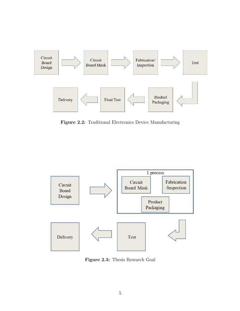
Figure 2.2: Traditional Electronics Device Manufacturing
Figure 2.3: Thesis Research Goal
5
2.2.2 Printed Electronics
There are many motivations for printed electronics other than just uniting the worlds of
printing and electronics. Other reasons include lower costs and implementation for flexible
electronics, for example, wearable electronics or RFID Tags. There are also many processes
for printing electronics. These include offset printing, gravure printing, flexographic printing,
screen printing, and inkjet printing [9, 24]. Except for inkjet printing, the other processes are
conventional printing technologies [24]. We shall focus on the most promising and pursued
of the technologies, inkjet printing.
Inkjet Printing
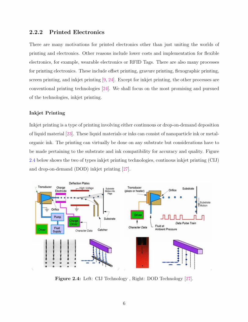
Inkjet printing is a type of printing involving either continuous or drop-on-demand deposition
of liquid material [23]. These liquid materials or inks can consist of nanoparticle ink or metal-
organic ink. The printing can virtually be done on any substrate but considerations have to
be made pertaining to the substrate and ink compatibility for accuracy and quality. Figure
2.4 below shows the two of types inkjet printing technologies, continous inkjet printing (CIJ)
and drop-on-demand (DOD) inkjet printing [27].
Figure 2.4: Left: CIJ Technology , Right: DOD Technology [27].
6
Continuous inkjet printing technology tends to be the most expensive due to printing head
cost and restrictive inkjet properties [27]. It does however print high frequency [27]. Drop-
on-demand inkjet printing technology has a cheaper head and better control of properties,
adding to the simplicity and compactness [27]. It also provides smaller droplets which aides
many electronic applications, thus making it a superior choice to CIJ technology [27].
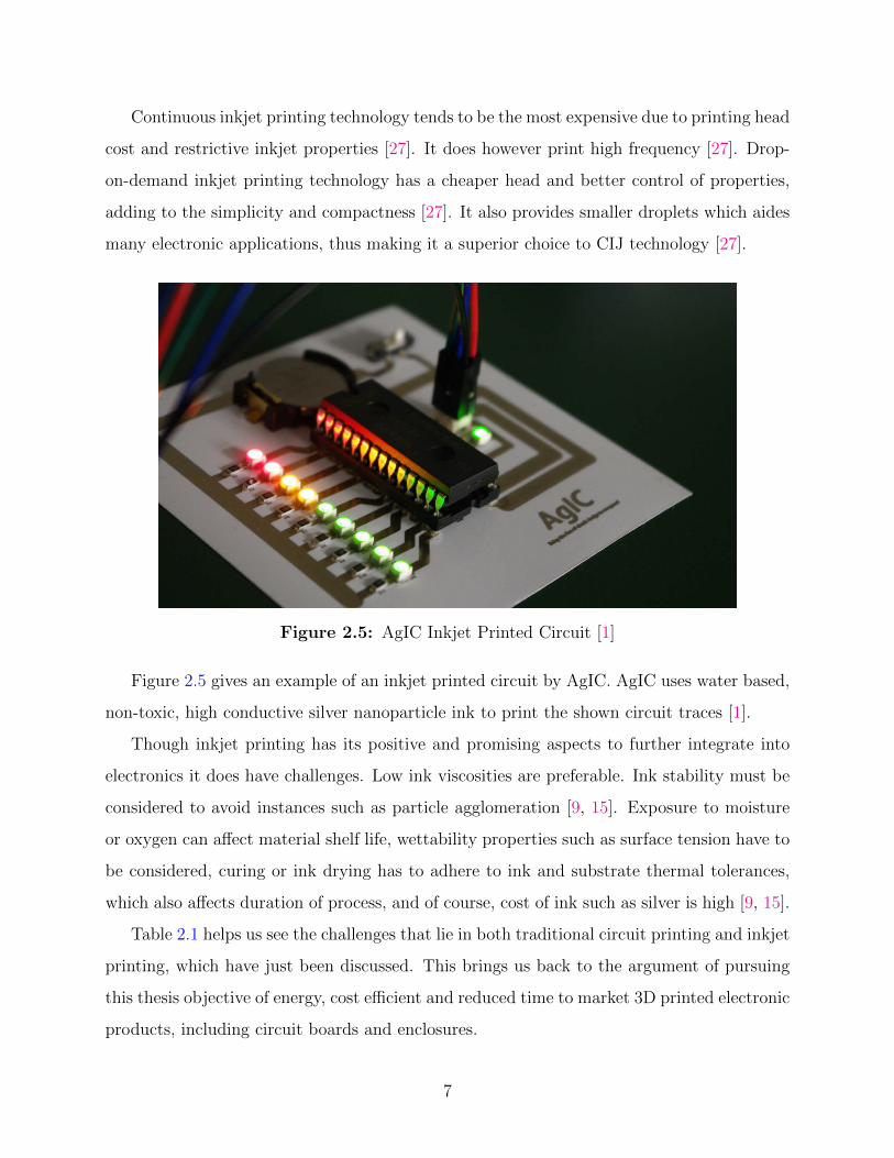
Figure 2.5: AgIC Inkjet Printed Circuit [1]
Figure 2.5 gives an example of an inkjet printed circuit by AgIC. AgIC uses water based,
non-toxic, high conductive silver nanoparticle ink to print the shown circuit traces [1].
Though inkjet printing has its positive and promising aspects to further integrate into
electronics it does have challenges. Low ink viscosities are preferable. Ink stability must be
considered to avoid instances such as particle agglomeration [9, 15]. Exposure to moisture
or oxygen can affect material shelf life, wettability properties such as surface tension have to
be considered, curing or ink drying has to adhere to ink and substrate thermal tolerances,
which also affects duration of process, and of course, cost of ink such as silver is high [9, 15].
Table 2.1 helps us see the challenges that lie in both traditional circuit printing and inkjet
printing, which have just been discussed. This brings us back to the argument of pursuing
this thesis objective of energy, cost efficient and reduced time to market 3D printed electronic
products, including circuit boards and enclosures.
7

Table 2.1: Challenges with Traditional and Inkjet Printing
Traditional Printing Inkjet printingHigh Cost Ink CostsHigh production Time Ink stability and ViscosityLarge Caron Footprint Curing Time
8

Chapter 3
3D Printer
This chapter contains information about how a 3D printer was selected; working to meet the
desired goal. A brief history and a function description is also included. Our approach is
to use Autodesk Fusion 360 as the design software to model the prints and Cura to prepare
the print for the printer, it was imperative to work with a printer that was compatible with
both environments [4, 26].
3.1 Series 1 Pro
Initially the Series 1 Pro, shown in figure 3.1, was chosen in the effort of printing the
3D circuits. Features include: 1.75mm extrusion head with 300 C maximum extruder
temperature, a build volume of 305 x 305 x 305 mm, on-board camera, Wi-Fi and Ethernet
capabilities, layer resolution range of 50-300 µm and free Cura for Type A machines [18]. In
spite of all these ideal features the Series 1 Pro possesses, the single head extruder would make
it impossible to print with two materials at the same time. This is a key requirement when
printing products with multiple materials, which includes conductive and non-conductive. It
was however used in the initial material analysis, which will be further discussed in chapter
4.
9
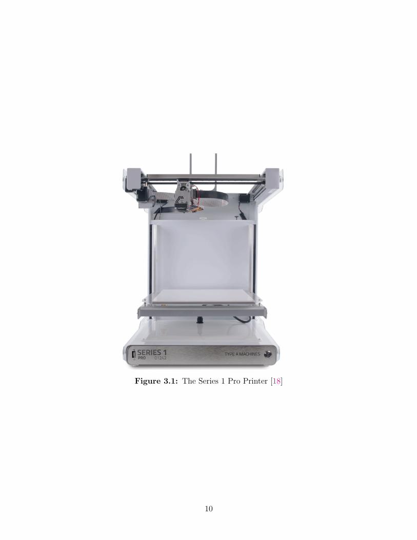
Figure 3.1: The Series 1 Pro Printer [18]
10
3.2 Ultimaker 3
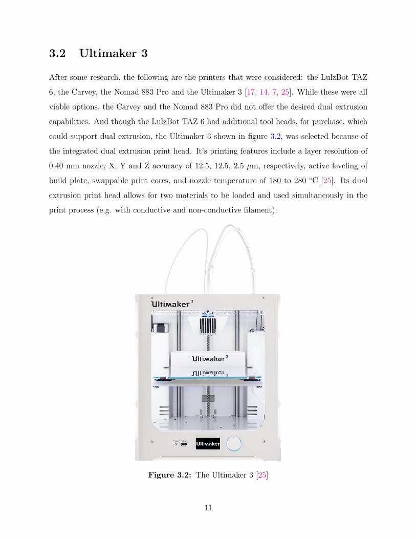
After some research, the following are the printers that were considered: the LulzBot TAZ
6, the Carvey, the Nomad 883 Pro and the Ultimaker 3 [17, 14, 7, 25]. While these were all
viable options, the Carvey and the Nomad 883 Pro did not offer the desired dual extrusion
capabilities. And though the LulzBot TAZ 6 had additional tool heads, for purchase, which
could support dual extrusion, the Ultimaker 3 shown in figure 3.2, was selected because of
the integrated dual extrusion print head. It’s printing features include a layer resolution of
0.40 mm nozzle, X, Y and Z accuracy of 12.5, 12.5, 2.5 µm, respectively, active leveling of
build plate, swappable print cores, and nozzle temperature of 180 to 280 C [25]. Its dual
extrusion print head allows for two materials to be loaded and used simultaneously in the
print process (e.g. with conductive and non-conductive filament).
Figure 3.2: The Ultimaker 3 [25]
11

Chapter 4
Conductive Material
In this chapter, the conductive polymer filament evaluated for the research goals will be
introduces and discussed.
Additive manufacturing utilizes materials/filament such as metal and plastic as its
building block. These materials include ( but not limited to) silver, aluminum, steel, paper,
acrylonitrile butadiene styrene (ABS), nylon, polylactide (PLA) and polyvinyl alcohol (PVA)
[28]. For this research, two types of polymer filaments were evaluated for use, ABS and PLA.
4.1 Acrylonitrile Butadiene Styrene (ABS)
ABS is an opaque, strong, somewhat flexible, and low cost thermoplastic [28, 16]. It can
be used for personal projects, concept and functional models, tooling, as well as general
manufacturing [16]. Conductive options of ABS were explored from various manufacturers
and distributors.
4.1.1 Conductive ABS
Two distributors were identified to supply conductive ABS , Robotshop and Alchement.
The Robotshop conductive ABS did not have any resistivity specification listed [22]. The
Alchement Conductive ABS volume resistivity specification was listed as 128 Ω-cm with
printing temperatures of 230 C to 250 C [2].
12
4.2 Polyactide (PLA)
Polyactide (PLA) is derived from fermented plant starch and thus biodegradable. This also
makes it a cost efficient thermoplastic, with applications similar to ABS, from do-it-yourself
projects to general manufacturing [8, 28].
4.2.1 Conductive PLA
Proto-Pasta and Black Magic 3D are manufacturers we identified for their conductive PLA.
Proto-Pasta had a Composite PLA - Electrically Conductive Graphite (ECG) filament. Their
product specification had the following volume resistivity; 15 Ω-cm pre- 3D printed resin, 30
Ω-cm 3D printed parts along layers in the X, Y dimension and 115 Ω-cm 3D printed parts
against layers in Z dimension [21]. The recommended printing temperatures were listed from
190 - 200 C. Black Magic 3D had a Conductive Graphene PLA Filament with a volume
resistivity of 0.6 Ω-cm and printing temperature of 195 - 220 C [6]. Table 4.1 below shows
a volume resistivity and printing temperatures of the materials discussed.
Table 4.1: Material Properties (* Specifications are incomplete given the cross- sectionareas are not provided)
CompositePLA Filament
ConductiveGraphenePLA Filament
ConductiveABS Filament(Alchement)
ConductiveABSFilament(Robot-shop)
Volumeresistivity *
30 Ω-cm 0.6 Ω-cm 128 Ω-cm -
ExtruderTemperature
190 - 200 C 195 - 220 C 230 - 250 C -
Predicting that resistivity would change contingent with the type of print that was needed
for this research. Also given that resistivity specifications were incomplete for the cross-
section areas of the materials, further analysis had to be done. The next chapter will discuss
filament analysis done to attain electronic properties for each materials.
13
Chapter 5
Printed Filament Analysis
In this chapter, discussed is the process of determining which of the chosen filaments would
be most suitable to perform the task of 3D printing a functioning circuit.
5.1 Resistance Analysis
5.1.1 Filament Model
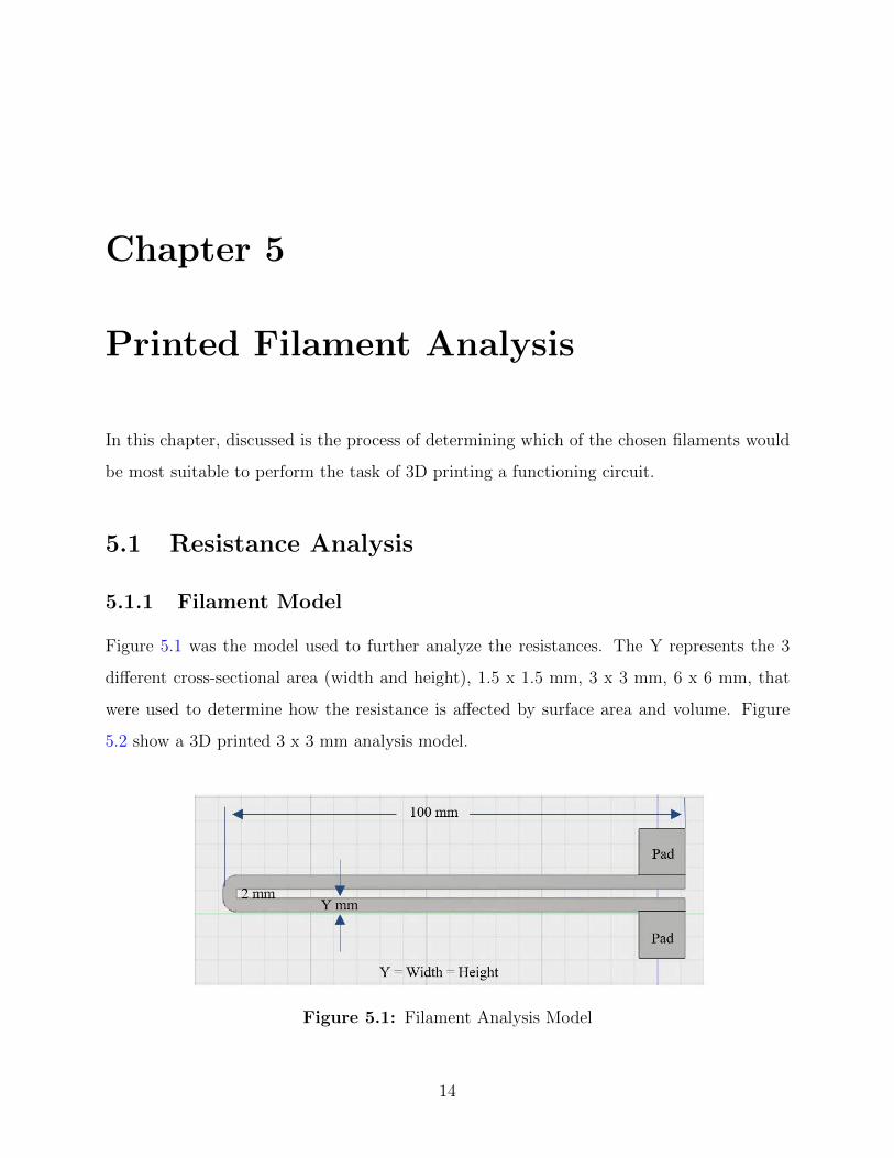
Figure 5.1 was the model used to further analyze the resistances. The Y represents the 3
different cross-sectional area (width and height), 1.5 x 1.5 mm, 3 x 3 mm, 6 x 6 mm, that
were used to determine how the resistance is affected by surface area and volume. Figure
5.2 show a 3D printed 3 x 3 mm analysis model.
Figure 5.1: Filament Analysis Model
14
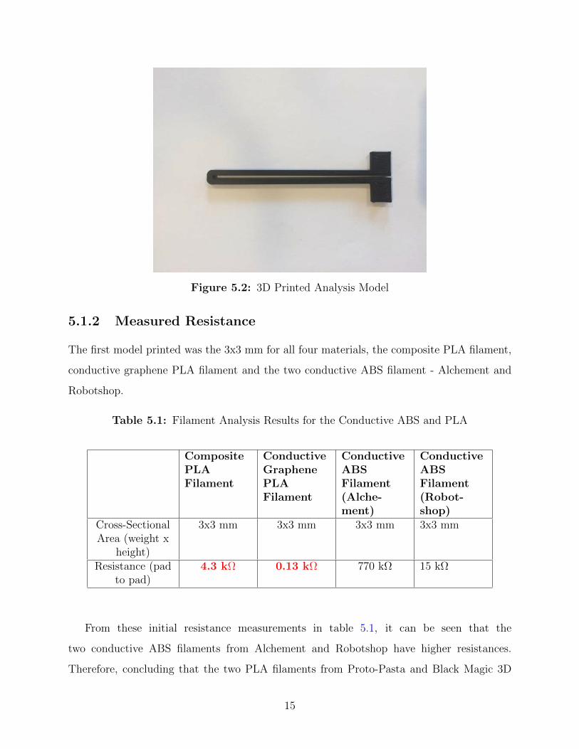
Figure 5.2: 3D Printed Analysis Model
5.1.2 Measured Resistance
The first model printed was the 3x3 mm for all four materials, the composite PLA filament,
conductive graphene PLA filament and the two conductive ABS filament - Alchement and
Robotshop.
Table 5.1: Filament Analysis Results for the Conductive ABS and PLA
CompositePLAFilament
ConductiveGraphenePLAFilament
ConductiveABSFilament(Alche-ment)
ConductiveABSFilament(Robot-shop)
Cross-SectionalArea (weight x
height)
3x3 mm 3x3 mm 3x3 mm 3x3 mm
Resistance (padto pad)
4.3 kΩ 0.13 kΩ 770 kΩ 15 kΩ
From these initial resistance measurements in table 5.1, it can be seen that the
two conductive ABS filaments from Alchement and Robotshop have higher resistances.
Therefore, concluding that the two PLA filaments from Proto-Pasta and Black Magic 3D
15

would be the ideal choice for further analysis, owing to their lower resistances. With this
information, printing and measurements with the other models (1.5x1.5 mm and 6x6 mm)
were conducted for both the composite PLA filament and conductice graphene PLA filament.
These measurements helped us better understand how resistance varies with the different
widths and heights of the models. Table 5.2 below, shows a comparison of the resistances
measured for all of the three models of the conductive PLA filaments.
Table 5.2: Filament Analysis Results for the Conductive PLA
CompositePLA Filament
ConductiveGraphenePLA Filament
Cross-SectionalArea (weight x
height)
Resistance (pad to pad)
1.5 x 1.5 mm 13 kΩ 0.48 kΩ3 x 3 mm 4.3 kΩ 0.13 kΩ6 x 6 mm 1.1 kΩ 0.04 kΩ
As shown above, as the widths and heights increase, the resistance decreases. Though
this new knowledge gave us some insight, we had to further analyze whether resistance varied
with volume or surface area.
5.1.3 Volume(Vol) and Surface Area(S.A.) in relation to Resis-
tance
Below are surface area and volume calculations of the analysis model with the three different
widths and heights of 1.5 x 1.5 mm , 3 x 3 mm and 6 x 6 mm. The models length is held
constant at approximately 202 mm.
1.5 x 1.5 mm Calculations
S.A. = 4 × 1.5 × 202 = 1212mm2 (5.1)
16
V ol = 1.5 × 1.5 × 202 = 454.5mm3 (5.2)
3 x 3 mm Calculations
S.A. = 4 × 3 × 202 = 2424mm2 (5.3)
V ol = 3 × 3 × 202 = 1818mm3 (5.4)
6 x 6 mm Calculations
S.A. = 4 × 6 × 202 = 4848mm2 (5.5)
V ol = 6 × 6 × 202 = 7272mm3 (5.6)
Using the 6x6 mm model as reference, a resistance surface area and resistance volume
was calculated. This was achieved by multiplying the measured resistances from both
conductive PLAs of the 6 x 6 mm model with its corresponding volume and surface area
as seen in equations 5.7, 5.10, 5.13 and 5.16. Then using the resulting surface area and
volume resistance factors divided by the 1.5 x 1.5 mm and 3 x 3 mm surface areas and
volumes (equations: 5.8, 5.9, 5.11, 5.12, 5.14, 5.15, 5.17, and 5.18), calculations were done
to determine if there was a strong relationship between the resistance and surface area or
volume.
6 x 6 mm Conductive Graphene PLA Resistance Volume
0.04kΩ × 7272mm3 = 290.9kΩ.mm3 (5.7)
Using this volume resistance factor of the 6x6 mm model and dividing it with the volumes
of the 1.5 x 1.5 mm and 3 x 3 mm to determine a calculated resistance comparison to the
measured values of the models.
R(3x3) = 290.9kΩ.mm3/1818mm3 = 0.16kΩ (5.8)
R(1.5x1.5) = 290.9kΩ.mm3/454.5mm3 = 0.64kΩ (5.9)
17
6 x 6 mm Conductive Graphene PLA Resistance Surface Area
0.04kΩ × 4848mm2 = 193.9kΩ.mm2 (5.10)
Using this surface area resistance factor of the 6x6 mm model and dividing it with the surface
areas of the 1.5 x 1.5 mm and 3 x 3 mm to determine a calculated resistance comparison to
the measured values of the models.
R(3x3) = 193.9kΩ.mm3/2424mm2 = 0.08kΩ (5.11)
R(1.5x1.5) = 290.9kΩ.mm3/1212mm2 = 0.16kΩ (5.12)
6 x 6 mm Composite PLA Resistance Volume
1.1kΩ × 7272mm3 = 7999kΩ.mm3 (5.13)
Using this volume resistance factor of the composite PLA 6x6 mm model and dividing it
with the volumes of the 1.5 x 1.5 mm and 3 x 3 mm to determine a calculated resistance
comparison to the measured values of the models.
R(3x3) = 7999kΩ.mm3/1818mm3 = 4.4kΩ (5.14)
R(1.5x1.5) = 7999kΩ.mm3/454.5mm3 = 17.6kΩ (5.15)
6 x 6 mm Composite PLA Resistance Surface Area
1.1KΩ × 4848mm2 = 5333kΩ.mm2 (5.16)
Using this surface area resistance factor of the composite PLA 6x6 mm model and dividing it
with the surface areas of the 1.5 x 1.5 mm and 3 x 3 mm to determine a calculated resistance
comparison to the measured values of the models.
R(3x3) = 5333kΩ.mm3/2424mm2 = 2.2kΩ (5.17)
R(1.5x1.5) = 5333kΩ.mm3/1212mm2 = 4.4kΩ (5.18)
18

Measured Resistance Analysis Conclusion
Comparing the calculated resistances above with that of table 5.2, it is observed that the
volume resistance factor yielded relatively close resistances to the measured values, compared
to that of the surface area resistance factor. Additionally, observing table 5.3 below (by the
colored text), provides that the volume has a stronger relationship with the resistance and it
was therefore concluded that resistance is affected by the volume of the material conducting
through the body of the material and not just the surface.
Table 5.3: Filament Analysis Results for the Conductive ABS and PLA
Composite PLA Filament Conductive Graphene PLA FilamentCross-SectionalArea (width xheight (mm))
1.5x1.5 3x3 6x6 1.5x1.5 3x3 6x6
S.A.(mm2) 1212 2424 4848 1212 2424 4848kΩ.(mm2) 15756 9454 5333 581.8 315.1 193.9Vol (mm3) 454.5 1818 7272 454.5 1818 7272kΩ.(mm3) 5909 7090 7999 218.2 236.3 290.9
Even though there is a strong relationship between the resistance and the volume, we
must note that the measurements did not give more accurate results. We can also see this
in the volume resistance calculations in table 5.3. Furthermore, it can be observed that the
conductive graphene PLA filament shows better accuracy than the composite PLA filament.
This could all be attributed to multiple reasons, which could include; lack of accuracy with
the material due to consistency of distribution of conductive particles during and after
the printing process, variations caused by print temperature and cooling, size/density of
conductive particles in the material, and capacitive load. Its possible this accuracy can be
further improved by increasing the model dimension’s width and heights.
19

Chapter 6
The Circuit Printing Process
In this chapter, the process of 3D printing the chosen circuit concepts is discussed and the
challenges encountered.
6.1 Concept Circuits
Two circuits were selected to implement the proposed 3D printing technology. The analog
and digital circuits in figure 6.1 are the concept circuits.
Figure 6.1: Left: The Analog Circuit Concept , Right: The Digital Circuit Concept [11].
6.2 Material Analysis for Print Process
With the circuits chosen, it was decided to first concentrate on the digital circuit, given
it would be less susceptible to resistance in the traces. Therefore printing analysis of the
20
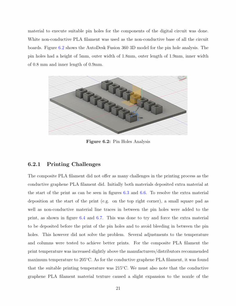
material to execute suitable pin holes for the components of the digital circuit was done.
White non-conductive PLA filament was used as the non-conductive base of all the circuit
boards. Figure 6.2 shows the AutoDesk Fusion 360 3D model for the pin hole analysis. The
pin holes had a height of 5mm, outer width of 1.8mm, outer length of 1.9mm, inner width
of 0.8 mm and inner length of 0.9mm.
Figure 6.2: Pin Holes Analysis
6.2.1 Printing Challenges
The composite PLA filament did not offer as many challenges in the printing process as the
conductive graphene PLA filament did. Initially both materials deposited extra material at
the start of the print as can be seen in figures 6.3 and 6.6. To resolve the extra material
deposition at the start of the print (e.g. on the top right corner), a small square pad as
well as non-conductive material line traces in between the pin holes were added to the
print, as shown in figure 6.4 and 6.7. This was done to try and force the extra material
to be deposited before the print of the pin holes and to avoid bleeding in between the pin
holes. This however did not solve the problem. Several adjustments to the temperature
and columns were tested to achieve better prints. For the composite PLA filament the
print temperature was increased slightly above the manufacturers/distributors recommended
maximum temperature to 205C. As for the conductive graphene PLA filament, it was found
that the suitable printing temperature was 215C. We must also note that the conductive
graphene PLA filament material texture caused a slight expansion to the nozzle of the
21

printer from wear, which we had to switch out (detachable nozzles) when we printed with
the composite PLA filament. This affected the print resolution for the conductive graphene
PLA filament.
Though the printing temperatures helped to a certain degree with the above mentioned
challenges, we still had to take further measures to ensure that the pin holes would print
according to the 3D model design. The the bottoms of the pin holes were beveled 0.5 -
1 mm, figure 6.8 shows the resulting print with the beveling. A line trace was added for
extra measure. With this result, we were more confident to proceed with printing the digital
circuit.
Figure 6.3: Conductive Graphene PLA Filament Pin Holes challenges 1
22
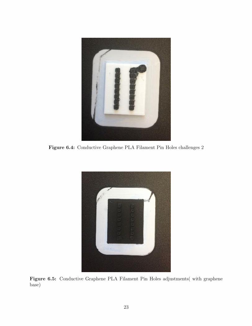
Figure 6.4: Conductive Graphene PLA Filament Pin Holes challenges 2
Figure 6.5: Conductive Graphene PLA Filament Pin Holes adjustments( with graphenebase)
23

Figure 6.6: Composite PLA Filament Pin Holes challenges 1
Figure 6.7: Composite PLA Filament Pin Holes challenges 2
24

Figure 6.8: Composite PLA Filament Pin Holes adjustments
25
Chapter 7
Circuit Analysis and Tests
In chapter 7, discussed are the results of printing digital circuit in both the composite PLA
and the conductive graphene PLA filaments. Analysis is also done to determine conductivity.
7.1 Digital Circuit on Breadboard
We first built the digital circuit concept shown in figure 7.1, on an actual breadboard with
the electronic components that would be used for the printed digital circuits. The electronic
components consisted of:
• A Common Cathode 7 Segment Display
• Seven 4.7 kΩ Series Resistors
• Four Switches
• Four 1.5 kΩ Pull-Up Resistors
• A 74LS48 BCD to 7 Segment Decoder
26
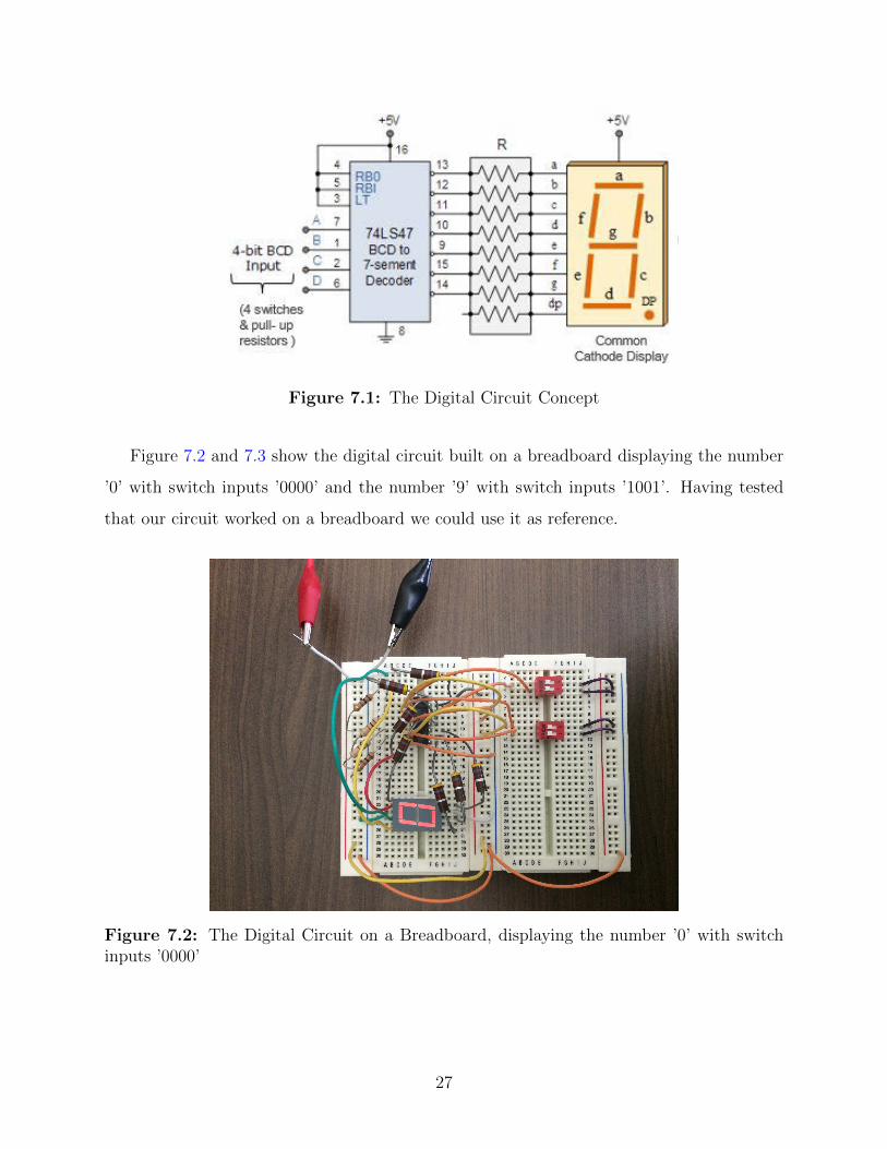
Figure 7.1: The Digital Circuit Concept
Figure 7.2 and 7.3 show the digital circuit built on a breadboard displaying the number
’0’ with switch inputs ’0000’ and the number ’9’ with switch inputs ’1001’. Having tested
that our circuit worked on a breadboard we could use it as reference.
Figure 7.2: The Digital Circuit on a Breadboard, displaying the number ’0’ with switchinputs ’0000’
27
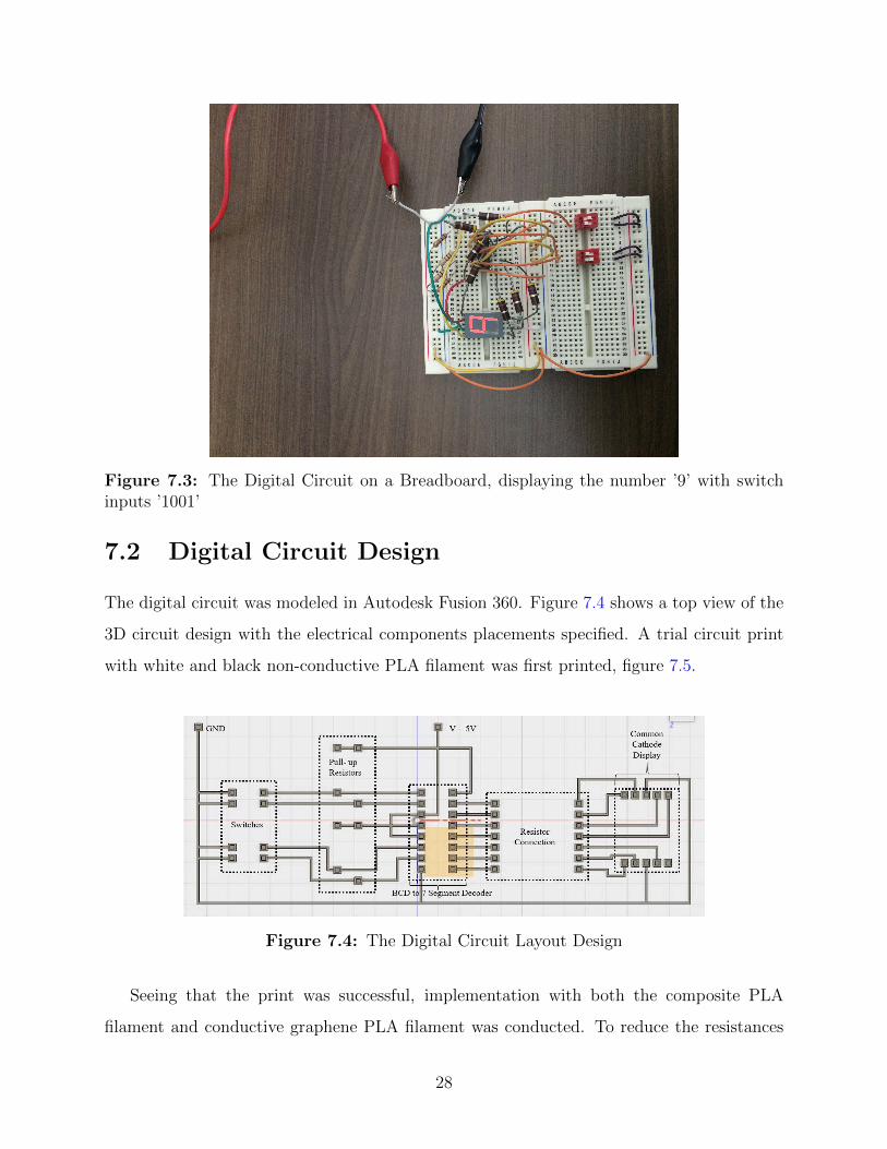
Figure 7.3: The Digital Circuit on a Breadboard, displaying the number ’9’ with switchinputs ’1001’
7.2 Digital Circuit Design
The digital circuit was modeled in Autodesk Fusion 360. Figure 7.4 shows a top view of the
3D circuit design with the electrical components placements specified. A trial circuit print
with white and black non-conductive PLA filament was first printed, figure 7.5.
Figure 7.4: The Digital Circuit Layout Design
Seeing that the print was successful, implementation with both the composite PLA
filament and conductive graphene PLA filament was conducted. To reduce the resistances
28
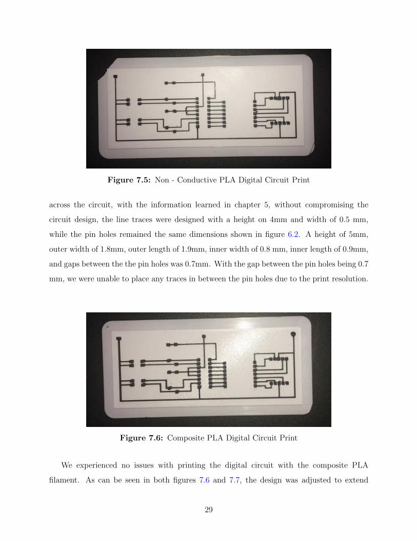
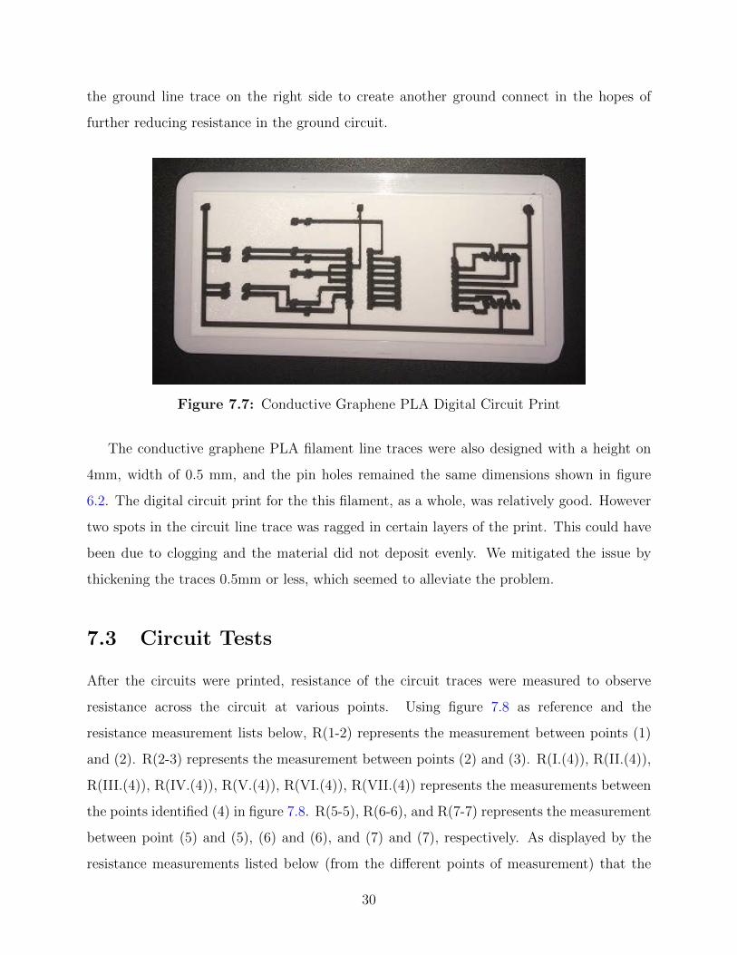
Figure 7.5: Non - Conductive PLA Digital Circuit Print
across the circuit, with the information learned in chapter 5, without compromising the
circuit design, the line traces were designed with a height on 4mm and width of 0.5 mm,
while the pin holes remained the same dimensions shown in figure 6.2. A height of 5mm,
outer width of 1.8mm, outer length of 1.9mm, inner width of 0.8 mm, inner length of 0.9mm,
and gaps between the the pin holes was 0.7mm. With the gap between the pin holes being 0.7
mm, we were unable to place any traces in between the pin holes due to the print resolution.
Figure 7.6: Composite PLA Digital Circuit Print
We experienced no issues with printing the digital circuit with the composite PLA
filament. As can be seen in both figures 7.6 and 7.7, the design was adjusted to extend
29
the ground line trace on the right side to create another ground connect in the hopes of
further reducing resistance in the ground circuit.
Figure 7.7: Conductive Graphene PLA Digital Circuit Print
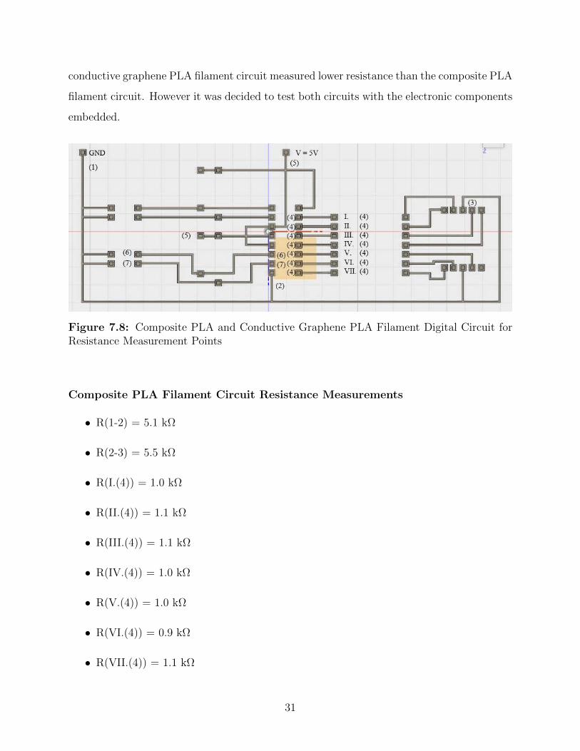
The conductive graphene PLA filament line traces were also designed with a height on
4mm, width of 0.5 mm, and the pin holes remained the same dimensions shown in figure
6.2. The digital circuit print for the this filament, as a whole, was relatively good. However
two spots in the circuit line trace was ragged in certain layers of the print. This could have
been due to clogging and the material did not deposit evenly. We mitigated the issue by
thickening the traces 0.5mm or less, which seemed to alleviate the problem.
7.3 Circuit Tests
After the circuits were printed, resistance of the circuit traces were measured to observe
resistance across the circuit at various points. Using figure 7.8 as reference and the
resistance measurement lists below, R(1-2) represents the measurement between points (1)
and (2). R(2-3) represents the measurement between points (2) and (3). R(I.(4)), R(II.(4)),
R(III.(4)), R(IV.(4)), R(V.(4)), R(VI.(4)), R(VII.(4)) represents the measurements between
the points identified (4) in figure 7.8. R(5-5), R(6-6), and R(7-7) represents the measurement
between point (5) and (5), (6) and (6), and (7) and (7), respectively. As displayed by the
resistance measurements listed below (from the different points of measurement) that the
30
conductive graphene PLA filament circuit measured lower resistance than the composite PLA
filament circuit. However it was decided to test both circuits with the electronic components
embedded.
Figure 7.8: Composite PLA and Conductive Graphene PLA Filament Digital Circuit forResistance Measurement Points
Composite PLA Filament Circuit Resistance Measurements
• R(1-2) = 5.1 kΩ
• R(2-3) = 5.5 kΩ
• R(I.(4)) = 1.0 kΩ
• R(II.(4)) = 1.1 kΩ
• R(III.(4)) = 1.1 kΩ
• R(IV.(4)) = 1.0 kΩ
• R(V.(4)) = 1.0 kΩ
• R(VI.(4)) = 0.9 kΩ
• R(VII.(4)) = 1.1 kΩ
31

• R(5-5) = 2.3 kΩ
• R(6-6) = 2.5 kΩ
• R(7-7) = 3.0 kΩ
Conductive Graphene PLA filament Circuit Resistance Measurements
• R(1-2) = 0.7 kΩ
• R(2-3) = 1.0 kΩ
• R(I.(4)) = 0.6 kΩ
• R(II.(4)) = 0.3 kΩ
• R(III.(4)) = 0.5 kΩ
• R(IV.(4)) = 0.3 kΩ
• R(V.(4)) = 0.6 kΩ
• R(VI.(4)) = 0.5 kΩ
• R(VII.(4)) = 1.0 kΩ
• R(5-5) = 0.8 kΩ
• R(6-6) = 0.6 kΩ
• R(7-7) = 0.5 kΩ
7.3.1 Implementation
The electronic components were laid for the composite PLA filament and conductive
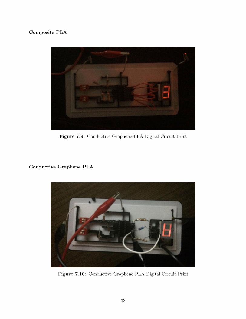
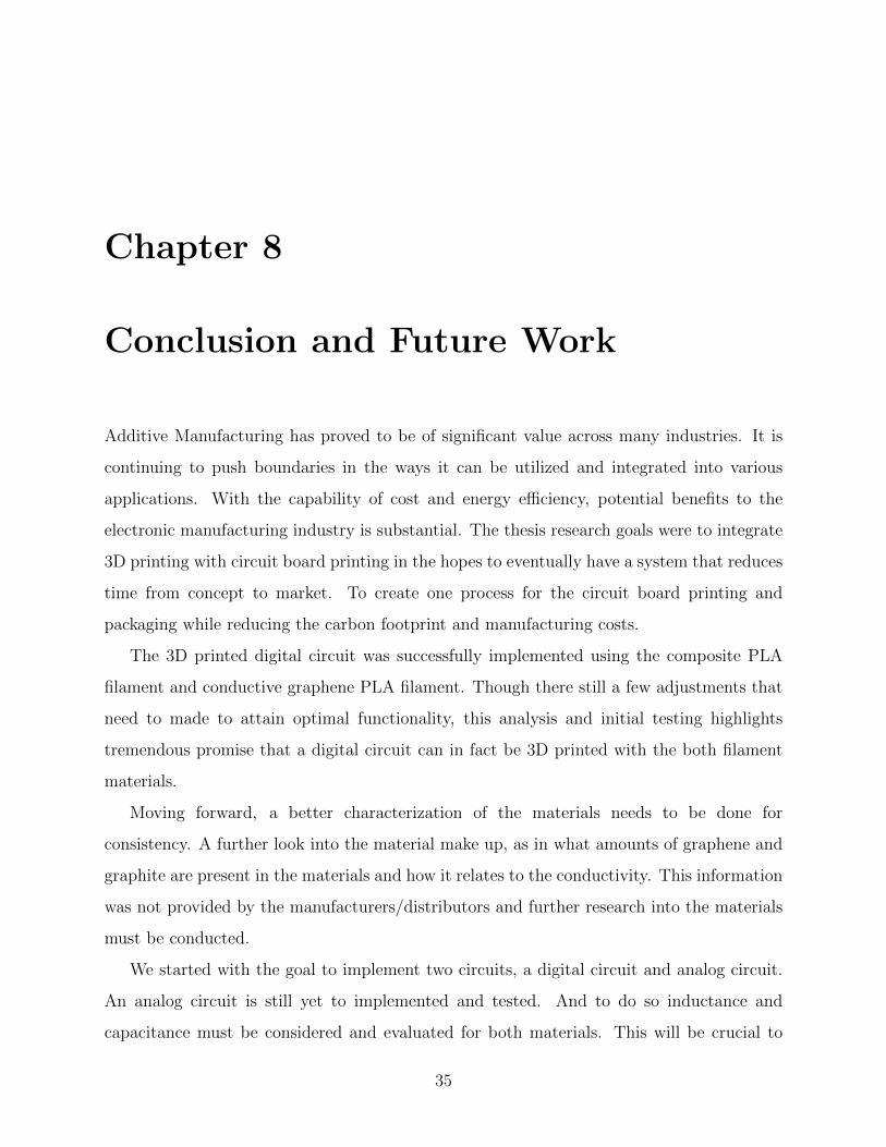
graphene PLA filament, and connected to the 5V power supply. This is displayed in figures
7.9 and 7.10. It can also be seen that there is an obvious response from the circuit, in terms
of connectivity, however the display did not switch numbers when prompted by the switches.
32
Composite PLA
Figure 7.9: Conductive Graphene PLA Digital Circuit Print
Conductive Graphene PLA
Figure 7.10: Conductive Graphene PLA Digital Circuit Print
33

There various possible reasons as to why the both circuits, shown in figure 7.9 and 7.10,
did not produce any other results when promoted by the switches. It could have been due
to different resistance the traces showed as seen in figure 7.8, causing poor conductance in
certain areas of the circuit. Furthermore, as we had discussed in section 7.2, the ragged traces
seen in the conductive graphene PLA filament print (figure 7.7) definitely created additional
resistance. Finally, we have not yet looked into a relationship between the material and its
capacitance and/or inductance, but it could have also played a role in impeding the flow of
current in some of the line traces.
34
Chapter 8
Conclusion and Future Work
Additive Manufacturing has proved to be of significant value across many industries. It is
continuing to push boundaries in the ways it can be utilized and integrated into various
applications. With the capability of cost and energy efficiency, potential benefits to the
electronic manufacturing industry is substantial. The thesis research goals were to integrate
3D printing with circuit board printing in the hopes to eventually have a system that reduces
time from concept to market. To create one process for the circuit board printing and
packaging while reducing the carbon footprint and manufacturing costs.
The 3D printed digital circuit was successfully implemented using the composite PLA
filament and conductive graphene PLA filament. Though there still a few adjustments that
need to made to attain optimal functionality, this analysis and initial testing highlights
tremendous promise that a digital circuit can in fact be 3D printed with the both filament
materials.
Moving forward, a better characterization of the materials needs to be done for
consistency. A further look into the material make up, as in what amounts of graphene and
graphite are present in the materials and how it relates to the conductivity. This information
was not provided by the manufacturers/distributors and further research into the materials
must be conducted.
We started with the goal to implement two circuits, a digital circuit and analog circuit.
An analog circuit is still yet to implemented and tested. And to do so inductance and
capacitance must be considered and evaluated for both materials. This will be crucial to
35

successfully printing a functioning analog circuit. Resistive precision is needed to adhere to
sensitivity that can be experienced with analog circuits. The lines traces will probably have to
be kept at minimum lengths and the distance between line traces increased to accommodate
sensitivity.
In conclusion, the advancements that have been made are proving to expose very strong
potential for integrating 3D printing with conductive polymers into electronic circuit printing
and manufacturing. Further opening doors to a world of applications from the automotive
industry, consumer electronics industry to the toy industry. This is only the beginning of an
electronic manufacturing revolution and evolution.
36

Bibliography
37

[1] AgIC (2014). Agic print - printing circuit boards with home printers.
[Online]. Available: https://www.kickstarter.com/projects/1597902824/
agic-print-printing-circuit-boards-with-home-print. ix, 7
[2] Alchement (2017). [star] alchement - abs conductive series, 3d filament,
1.75mm, 1kg (conductive). [Online]. Available: https://www.amazon.com/
STAR-Alchement-Conductive-Filament-1-75mm/dp/B01COH43R2/ref=sr_1_7?s=
industrial&ie=UTF8&qid=1472216725&sr=1-7&keywords=conductive+abs+filament.
12
[3] Association, C. T. (2014). Consumer electronics industry revenues to reach
all-time high in 2014, projects ceas semi-annual sales and forecasts report.
[Online]. Available: https://www.cta.tech/News/Press-Releases/2014/July/
Consumer-Electronics-Industry-Revenues-to-Reach-Al.aspx. 1
[4] AutoDesk (2017). Fusion 360. [Online]. Available: https://www.autodesk.com/
products/fusion-360/overview. 9
[5] Bensoussan, H. (2016). The history of 3d printing: 3d printing technologies from
the 80s to today. [Online]. Available: https://www.sculpteo.com/blog/2016/12/14/
the-history-of-3d-printing-3d-printing-technologies-from-the-80s-to-today/.
3
[6] BlackMagic3D (2017). Conductive graphene pla filament 100g. [Online]. Available:
https://www.blackmagic3d.com/Conductive-p/grphn-pla.htm. 13
[7] Carbide3D (2017). The nomad 883 pro. [Online]. Available: http://carbide3d.com/
nomad/. 11
[8] CreativeMechanisms (2016). Everything you need to know about polylactic
acid (pla). [Online]. Available: https://www.creativemechanisms.com/blog/
learn-about-polylactic-acid-pla-prototypes. 13
38

[9] Daniel, J. (2010). Printed electronics:technologies, challenges and
applications. [Online]. Available: https://www.parc.com/content/attachments/
printed-electronics-technologies.pdf. 6, 7
[10] Dyer, E. (2015). The world’s first 3d-printed car is a blast to drive.
[Online]. Available: http://www.popularmechanics.com/cars/a16726/
local-motors-strati-roadster-test-drive/. ix, 4
[11] ElectronicsTutorials (2017). Bcd counter circuit. [Online]. Available: http://www.
electronics-tutorials.ws/counter/bcd-counter-circuit.html. ix, 20
[12] EOS (2017). Additive manufacturing, laser-sintering and industrial 3d printing -
benefits and functional principle. [Online]. Available: https://www.eos.info/additive_
manufacturing/for_technology_interested. 3
[13] Hooper, T. (2017). The 7 biggest trends and challenges in the electronics
manufacturing industry in 2017. [Online]. Available: https://www.pannam.com/blog/
top-trends-and-challenges-in-electronics-manufacturing/. 1
[14] Inventables (2017). Carvey. [Online]. Available: https://www.inventables.com/
technologies/carvey. 11
[15] Kamyshny, A. and Magdassi, S. (2014). Conductive nanomaterials for printed
electronics. Small, 10(17):3515–3535. 1, 7
[16] Kulich, D. M., Gaggar, S. K., Lowry, V., and Stepien, R. (2001). Acrylonitrilebutadi-
enestyrene polymers. Polymers. Encyclopedia of Polymer Science and Technology. 12
[17] LulzBot (2017). Lulzbot taz 6. [Online]. Available: https://www.lulzbot.com/store/
printers/lulzbot-taz-6. 11
[18] Machines, T. A. (2017). Series 1 pro. [Online]. Available: https://www.
typeamachines.com/series-1-pro. ix, 9, 10
[19] Manufacturing, A. (2017). What is additive manufacturing. [Online]. Available: http:
//additivemanufacturing.com/basics/. 3
39

[20] of Exeter, T. U. (2017). The history of additive layer manufacturing. [Online]. Available:
http://emps.exeter.ac.uk/engineering/research/calm/whatis/history/. 3
[21] Proto-Pasta (2017). Composite pla - electrically conductive graphite. [Online].
Available: https://www.proto-pasta.com/products/conductive-pla. 13
[22] RobotShop (2017). conductive abs 250g 175mm filament
with spool. [Online]. Available: http://www.robotshop.com/en/
conductive-abs-250g-175mm-filament-with-spool.html. 12
[23] Singh, M., Haverinen, H. M., Dhagat, P., and Jabbour, G. E. (2010). Inkjet
printingprocess and its applications. Advanced Materials, 22:673–685. 6
[24] Sridhar, A., Blaudeck, T., and Baumann, R. (2011). Inkjet printing as a key enabling
technology for printed electronics. [Online]. Available: https://www.sigmaaldrich.com/
technical-documents/articles/material-matters/inkjet-printing-as.html. 6
[25] Ultimaker (2017). Ulitmaker 3. [Online]. Available: https://ultimaker.com/en/
products/ultimaker-3. ix, 11
[26] UltimakerCura (2017). Ultimaker cura software. [Online]. Available: https://
ultimaker.com/en/products/ultimaker-cura-software. 9
[27] Unijet (2009). Inkjet technology. [Online]. Available: http://www.unijet.co.kr/eng/
main/sub04_01.html. ix, 6, 7
[28] von Ubel, M. (2017). 3d printing materials guide 2017 the
complete overview. [Online]. Available: https://all3dp.com/1/
3d-printing-materials-guide-3d-printer-material/. 12, 13
[29] Wohlers, T. and Gornet, T. (2014). History of additive manufacturing. Technical report.
3
40
Vita
Mwamba Bowa was born and raised in Zambia. She moved to Knoxville, TN to attend the
University of Tennessee (UT) and pursue a degree in electrical engineering. She graduated
with her Bachelor of Science (B.S) in December 2015 and started as a Master’s student,
in the same field, that following spring. Mwamba works as Graduate Teaching Assistant
(GTA) for the senior design courses in the Electrical Engineering and Computer Science
(EECS) department while working on 3D printed electronics research. Outside her school
and research work, Mwamba is passionate about mentoring minorities and growing the
number of Women in STEM (Science, Technology, Engineering and Mathematics) fields,
specifically engineering. She served on the board of Systers: Women in EECS as the
secretary and a mentor. The mission of Systers is to recruit, mentor, and retain women in the
engineering field. She has also taught a one-hour credit seminar book study class on Sheryl
Sandbergs Lean In: For Graduates. The class covered crippling professional barriers that
exist between women and their professional goals, bridging the cultural gaps, professional
development topics and building community. Mwamba has also served as a freshman mentor
for the STEAM (Science, Technology, Engineering, Agriculture and Mathematics) minority
mentoring program, which is joint a collaboration between the College of Engineering, the
College of Agricultural Sciences and Natural Resources, and the Tennessee Louis Stokes
Alliance for Minority Participation (TLSAMP). Mwamba is looking forward to join the
engineering industry after graduation this fall 2017.
41
Related Documents