© 2012 CPI. All rights reserved CPI Printable Electronics The National Printed Electronics Centre Tom Taylor CIKC Event December 2012

Welcome message from author
This document is posted to help you gain knowledge. Please leave a comment to let me know what you think about it! Share it to your friends and learn new things together.
Transcript
© 2012 CPI. All rights reserved
CPI Printable Electronics
The National Printed Electronics Centre
Tom TaylorCIKC EventDecember 2012

About CPI – CATAPULT CENTREFirst UK Technology Innovation institute
2007 UK National Centre in Printable Electronics• 2011 First UK Technology Innovation Centre TIC• 50 employees• £30m investment to date
CPI - Centre for Process InnovationFounded in 2004
• 200 employees• £75M investment to date• UKs first Technology and Innovation Centre • Focus on:
– Sustainable Processing– High Temperature processing (>1000c)– Bio- Pharma biologics centre – December 2012 (£38m)– Printable Electronics

CPI Overview
CPI is a design, development and prototyping facility for the emerging Printable Electronics (PE) industry.
CPI offers equipment for scale up to full size
Our customers bring their problems, inventions, and innovative business ideas
CPI works with clients to bring new PE products and processes to market quickly and efficiently, by offering facilities and expertise that help reduce the level of R&D risk and capital investment.
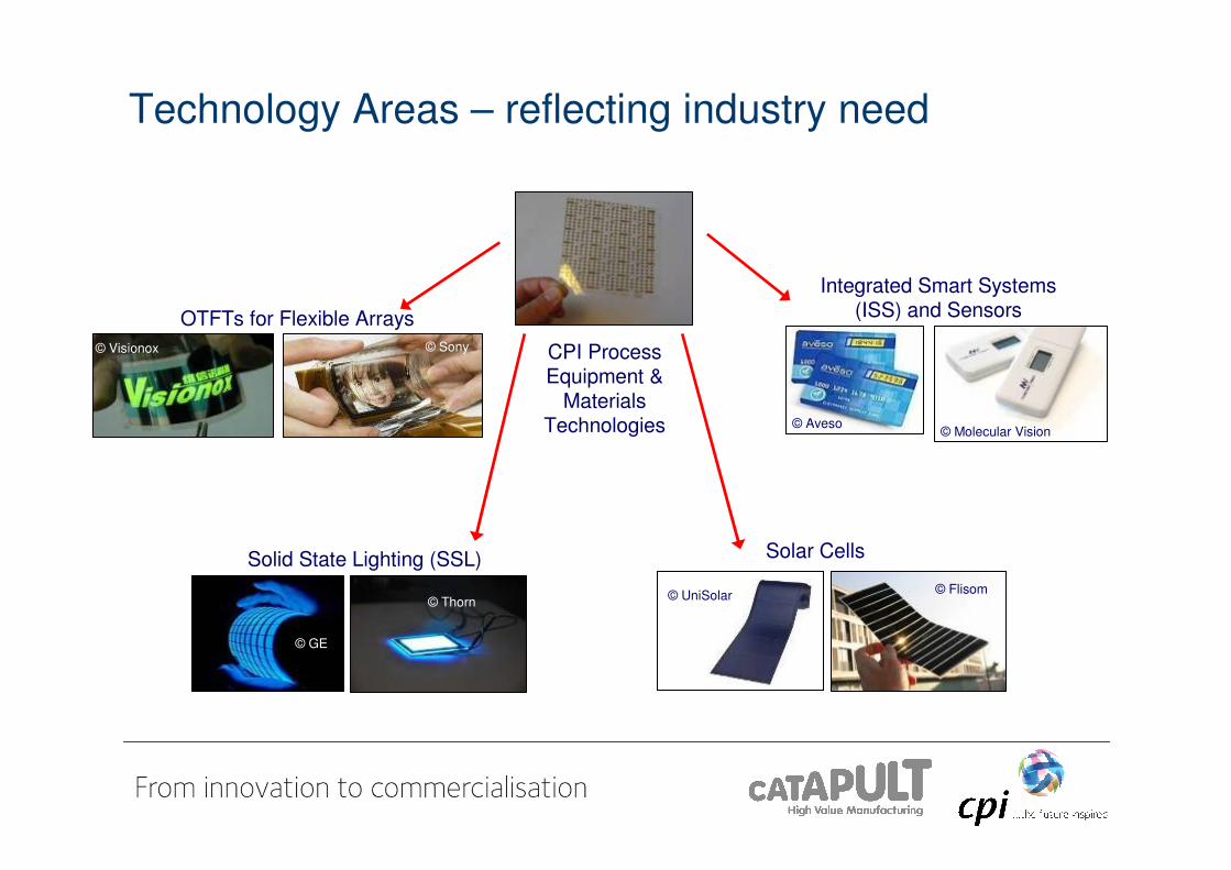
Technology Areas – reflecting industry need
CPI Process Equipment &
Materials Technologies
© Visionox © Sony
OTFTs for Flexible Arrays
© GE
© Thorn
Solid State Lighting (SSL)© Flisom© UniSolar
Solar Cells
© Aveso© Molecular Vision
Integrated Smart Systems (ISS) and Sensors
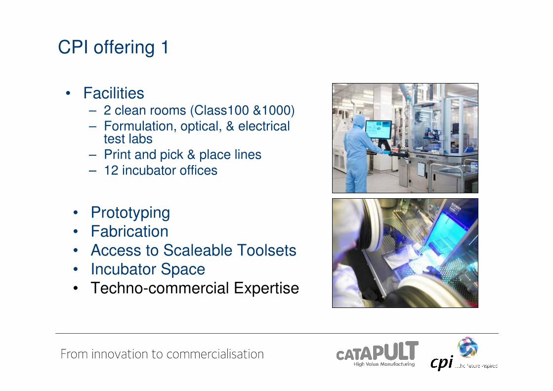
• Prototyping• Fabrication• Access to Scaleable Toolsets• Incubator Space• Techno-commercial Expertise
• Facilities– 2 clean rooms (Class100 &1000)– Formulation, optical, & electrical
test labs– Print and pick & place lines– 12 incubator offices
CPI offering 1
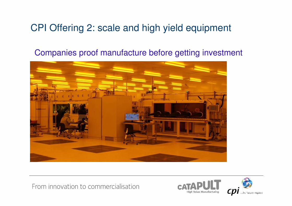
CPI Offering 2: scale and high yield equipment
Companies proof manufacture before getting investment
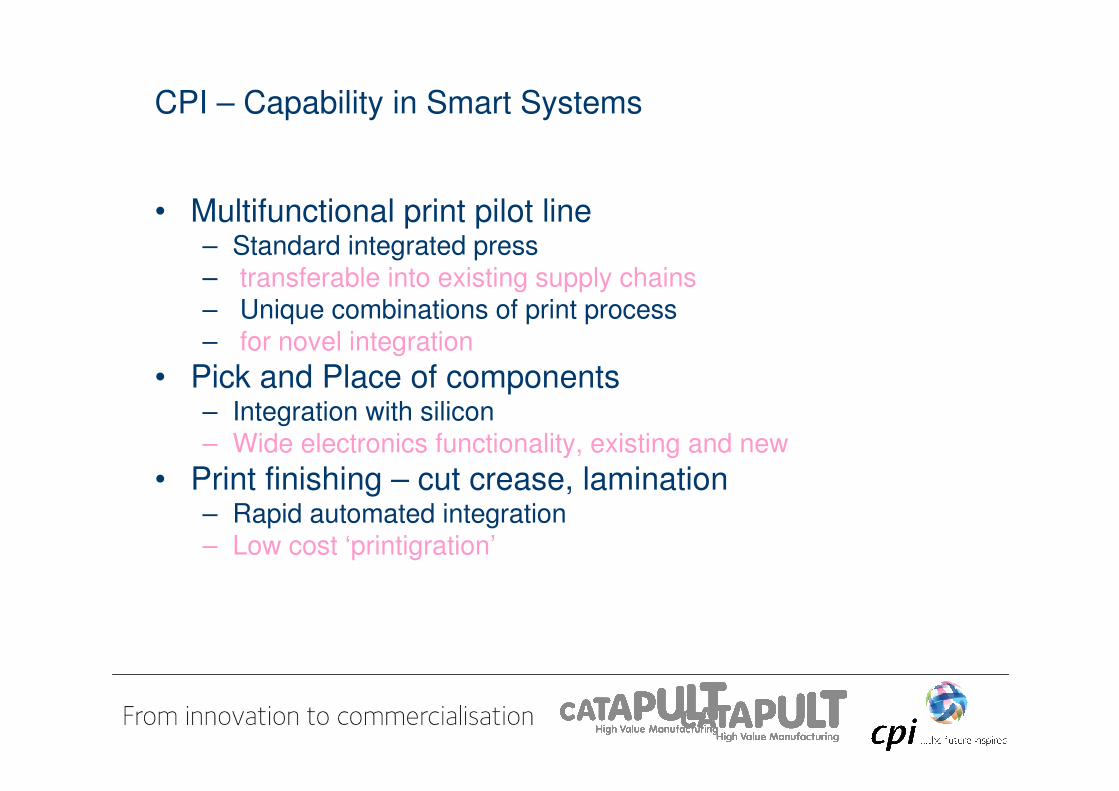
CPI – Capability in Smart Systems
• Multifunctional print pilot line– Standard integrated press– transferable into existing supply chains– Unique combinations of print process– for novel integration
• Pick and Place of components– Integration with silicon– Wide electronics functionality, existing and new
• Print finishing – cut crease, lamination– Rapid automated integration– Low cost ‘printigration’

•Flexo•Gravure •Offset litho •Rotary Screen •Narrow web (420mm) Nilpeter reel to reel printing press•Variety of substrate types 25-370 microns
Nilpeter Print Production Platform
Novalia images
Electronic Integration and rapid manufacture

Technology Focus: Transistor TFT arrays
1mm
0.1mm
1cm
• 106ppi e-paper backplane
• Produced on a glass substrate
• 6 micron minimum feature, 5 micron design rule (overlay accuracy)
• 3” (75mm) diagonal, 48,000 transistors
Display, sensors, micro circuitry
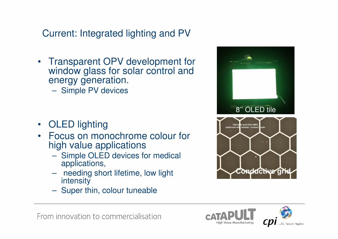
Current: Integrated lighting and PV
• Transparent OPV development for window glass for solar control and energy generation. – Simple PV devices
• OLED lighting • Focus on monochrome colour for
high value applications– Simple OLED devices for medical
applications,– needing short lifetime, low light
intensity– Super thin, colour tuneable
8’’ OLED tile
Conductive grid

Case Study: Change in form factor
• Used: CPI’s R2R Sputter coater, Epigem dip coating, Tata roll coating at Shotton
• Next Steps: Tata development programme: at SPECIFIC in Swansea, & Shotton PV Accelerator
• Using conventional roll printing and screen printing processes onto steel,
Integrated Photovoltaic : Development of DSSC roof sheets on steel encapsulated with R2R produced Barrier Film
Large Area PV Cells on Steel Roof
Tata Steel

Case study: device integration
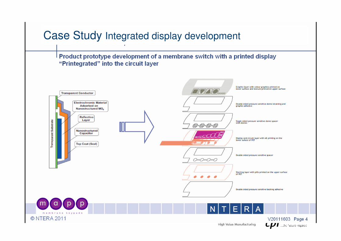
Case Study Integrated display development
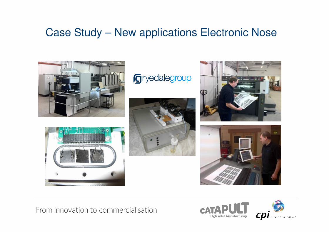
Case Study – New applications Electronic Nose
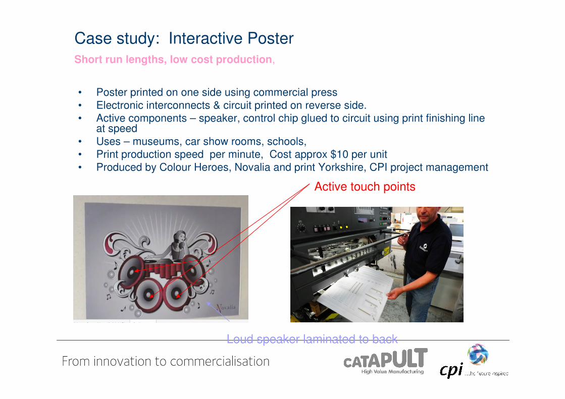
Case study: Interactive PosterShort run lengths, low cost production,
• Poster printed on one side using commercial press• Electronic interconnects & circuit printed on reverse side.• Active components – speaker, control chip glued to circuit using print finishing line
at speed• Uses – museums, car show rooms, schools,• Print production speed per minute, Cost approx $10 per unit• Produced by Colour Heroes, Novalia and print Yorkshire, CPI project management
Active touch points
Loud speaker laminated to back

Printed Electronics competencies at CPI
• Formulation – Enables the development of functional inks for printed electronics, including metals,
dielectrics, polymers, substrate – generic to most projects
• Coating – Fine coating applications of extreme uniformity and continuity for high yield
electronics applications using evaporation and solution methods - generic to most projects
• Encapsulation – Barrier film, edge seal, in-situ encapsulation – generic to most projects
• Device Testing– OLED, TFT, and Smart device testing of device elements and formulations –
barrier measurement
• Process Engineering– Electronics fab, plastic and print process – 12 experienced engineers in this field
Summary
• CPI UK National Printed Electronics centre, reflected in £30m investment 2008-11
• Equipped with industry relevant toolsets operated by industry focused personnel
• Shown the Development and introduction of smart products using AVAILABLE TECHNOLOGY
• Simple products with unique features

www.uk-cpi.com
Thanks for your kind attention
Tom Taylor
Related Documents