21/03/2003 ULIS 2003 - Udine (Italy) - C. Gallon 1 Analysis of Mechanical Stress Effects in Short Channel MOSFETs C. Gallon 1 , G. Reimbold 1 , G. Ghibaudo 2 , R.A. Bianchi 3 and R. Gwoziecki 1,3 . 1 CEA-Leti, 38054 Grenoble Cedex 9, France. Tel. : +33 (0)4 38 78 49 93. E-mail: [email protected] 2 IMEP, BP257, 38016 Grenoble Cedex 9, France. 3 STMicroelectronics, Central R&D, 38921 Crolles, France.

21/03/2003 ULIS 2003 - Udine (Italy) - C. Gallon 1 Analysis of Mechanical Stress Effects in Short Channel MOSFETs C. Gallon 1, G. Reimbold 1, G. Ghibaudo.
Dec 19, 2015
Welcome message from author
This document is posted to help you gain knowledge. Please leave a comment to let me know what you think about it! Share it to your friends and learn new things together.
Transcript

21/03/2003 ULIS 2003 - Udine (Italy) - C. Gallon 1
Analysis of Mechanical Stress Effects in Short Channel MOSFETs
C. Gallon1, G. Reimbold1, G. Ghibaudo2, R.A. Bianchi3 and R. Gwoziecki1,3.
1CEA-Leti, 38054 Grenoble Cedex 9, France. Tel. : +33 (0)4 38 78 49 93. E-mail: [email protected]
2IMEP, BP257, 38016 Grenoble Cedex 9, France. 3STMicroelectronics, Central R&D, 38921 Crolles, France.

21/03/2003 ULIS 2003 - Udine (Italy) - C. Gallon 2
OUTLINE
• Introduction
• Experimental Method– Four point bending technique
– Tested devices
• Experimental Results:– Stress Influence on Long Channel Devices
– Stress Influence on Short Channel Devices
• Conclusion and Perspectives

21/03/2003 ULIS 2003 - Udine (Italy) - C. Gallon 3
INTRODUCTION (1)• Context:
– Generation of mechanical stress at various process steps.
– These effects are more important in scaled CMOS devices
– A key role of mechanical stress in MOSFETs devices:
Performance improvements (SiGe, SiGe:C… )
or Performance reductions (STI,…)
• Needs:– Improve extraction methodologies versus mechanical stress.
– Better understanding and evaluation of stress effects onMOSFETs devices.

21/03/2003 ULIS 2003 - Udine (Italy) - C. Gallon 4
INTRODUCTION (2)
• Purpose of this work:
– Analysis of external mechanical stress effects on
MOSFETs from advanced 0.13µm CMOS technology:
Relative variations of mobility with external stress,
Extraction of Piezoresistive Response (PR),
Simple approach proposed to extract PR on short devices accounting for Rsd influence.
– Objectives: Try to provide data for device simulators and a better analysis of stress effects.
21/03/2003 ULIS 2003 - Udine (Italy) - C. Gallon 5
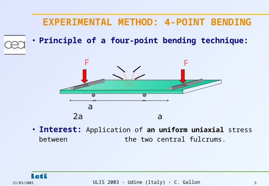
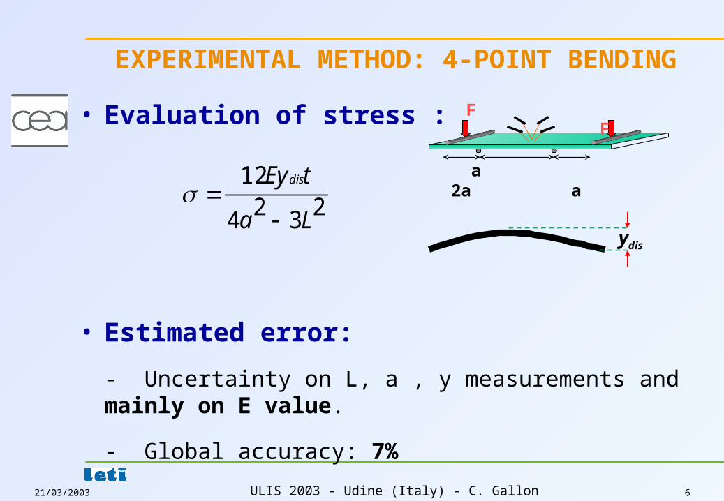
• Principle of a four-point bending technique:
• Interest: Application of an uniform uniaxial stress between
the two central fulcrums.
a 2a a
F F
EXPERIMENTAL METHOD: 4-POINT BENDING
21/03/2003 ULIS 2003 - Udine (Italy) - C. Gallon 6
2324
12
La
tEydis
ydis
• Evaluation of stress :
• Estimated error:
- Uncertainty on L, a , y measurements and mainly on E value.
- Global accuracy: 7%
a 2a a
F F
EXPERIMENTAL METHOD: 4-POINT BENDING
21/03/2003 ULIS 2003 - Udine (Italy) - C. Gallon 7
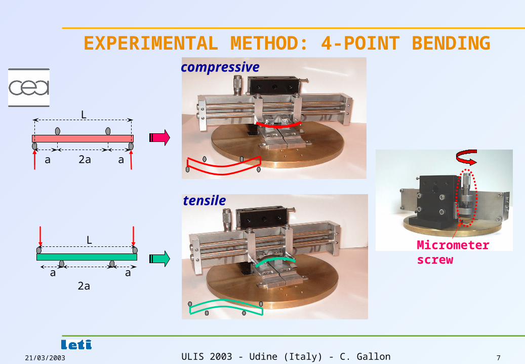
Micrometer screw
EXPERIMENTAL METHOD: 4-POINT BENDING
a a2a
L
2aa a
L
compressive
tensile

21/03/2003 ULIS 2003 - Udine (Italy) - C. Gallon 8
• Specific characteristics:
– Rectangular strip are cut from a saw technique.
– With an appropriate preparation of the strips, mechanical stress:
longitudinal direction (// to current flow)
or transversal direction ( to current flow).
– Most strips fail for 150-200MPa
Keep the applied mechanical stress below 100MPa.
EXPERIMENTAL METHOD: 4-POINT BENDING

21/03/2003 ULIS 2003 - Udine (Italy) - C. Gallon 9
• Bulk and SOI similar technologies- nMOS and pMOS fabricated on (100) substrates
- Tox=2nm; W=10µm; Long (L=10µm) or short (L=0.13µm) channel length;
- Important point on our short devices: a long distance between STI and gate
limit parasitic internal stress.
- Mechanical stress ranging from 0 to 100MPa was applied.
DEVICES TESTED ON 4-POINT BENDING
Substrate
Gate
DrainSource
Bulk Technology
Buried oxide
Substrate
Gate
DrainSource
SOI technology

21/03/2003 ULIS 2003 - Udine (Italy) - C. Gallon 10
EXPERIMENTAL RESULTS: Long Channel Devices
• Effects of mechanical stress on transfer characteristics
- Linear region characteristics of nMOS BULK:
- Use of standard expressions to extract VT and µ.
- Note the invariance of VT and mobility variations.
0
1
2
3
4
5
-0,5 0 0,5 1 1,5Vg (V)
Gm
(10-5
S)
Id@100MPa
Id@0MPa
0
1
2
3
4
5
-0,5 0 0,5 1 1,5Vg (V)
Gm
(10-5
S)
Id@100MPa
Id@0MPaId@0MPa
Id@100MPa
DVµCW
Slope oxL
2
D
T
VV
0
1
2
3
4
-0,5 0 0,5 1 1,5Vg (V)
Id (
10-5
A)
Id@0MPa
Id@100MPa
DVµCW
Slope oxL
2
D
T
VV
0
1
2
3
4
-0,5 0 0,5 1 1,5Vg (V)
Id (
10-5
A)
0
1
2
3
4
-0,5 0 0,5 1 1,5Vg (V)
Id (
10-5
A)

21/03/2003 ULIS 2003 - Udine (Italy) - C. Gallon 11
• Normalized mobility variations versus applied stress:
- Excellent linear dependence for both n and p MOS devices.
0
1
2
3
4
5
6
7
8
0 25 50 75 100Transversal
Longitudinal
SOI
BULK
nMOS
L=10µm W=10µm
0
1
2
3
4
5
6
7
8
0 25 50 75 100
SOI
BULK
0
1
2
3
4
5
6
7
8
0 25 50 75 1000
1
2
3
4
5
6
7
8
0 25 50 75 100Tensile Stress (MPa)
µ/µ
(%
)
-8
-202468
0 25 50 75 100
Longitudinal
SOI
02468
0 25 50 75 100
-6
02468
0 25 50 75 100
-4
02468
0 25 50 75 100
Transversal
pMOS
L=10µm W=10µm BULK
BULK
SOI
µ/µ
(%
)Tensile Stress (MPa)
EXPERIMENTAL RESULTS: Long Channel Devices

21/03/2003 ULIS 2003 - Udine (Italy) - C. Gallon 12
• Mobility variations and piezoresistance response:
L longitudinal coefficient
T transverse coefficient
Majors coefficients of cubic structure for silicon
2
44S
L0
µ
µ
2
44S
T90
µ
µ
//J
J
44,
12,
11
1211
S
EXPERIMENTAL RESULTS: Long Channel Devices
21/03/2003 ULIS 2003 - Udine (Italy) - C. Gallon 13
• Piezoresistance coefficients (.10-12Pa-1):
BULK SOI Errors
LnMOS
TnMOS
SnMOS
44nMOS
622
272
894
349
734
393
1127
341
40
40
60
60
LpMOS
TpMOS
SpMOS
44pMOS
-770
491
-280
-1261
-967
531
-435
-1499
40
40
60
60
Bulk&SOI results0.13µm techno.
EXPERIMENTAL RESULTS: Long Channel Devices
Bradley&al. IEEE20010.3µm techno. Ref. Si
-415
385
-30
-800
320
250
570
70
Texas Instr.
-600
400
-200
-1000
-500
450
-50
-950
LpMOS
TpMOS
SpMOS
44pMOS
500
350
850
150
450
350
800
100
LnMOS
TnMOS
SnMOS
44nMOS
Lucent Techno
IBM
-415
385
-30
-800
320
250
570
70
Texas Instr.
-600
400
-200
-1000
-500
450
-50
-950
LpMOS
TpMOS
SpMOS
44pMOS
500
350
850
150
450
350
800
100
LnMOS
TnMOS
SnMOS
44nMOS
Lucent Techno
IBM
-718
663
-55
-1380
311
175
486
136
Lightly doped Si
-718
663
-55
-1380
311
175
486
136
Lightly doped Si
21/03/2003 ULIS 2003 - Udine (Italy) - C. Gallon 14
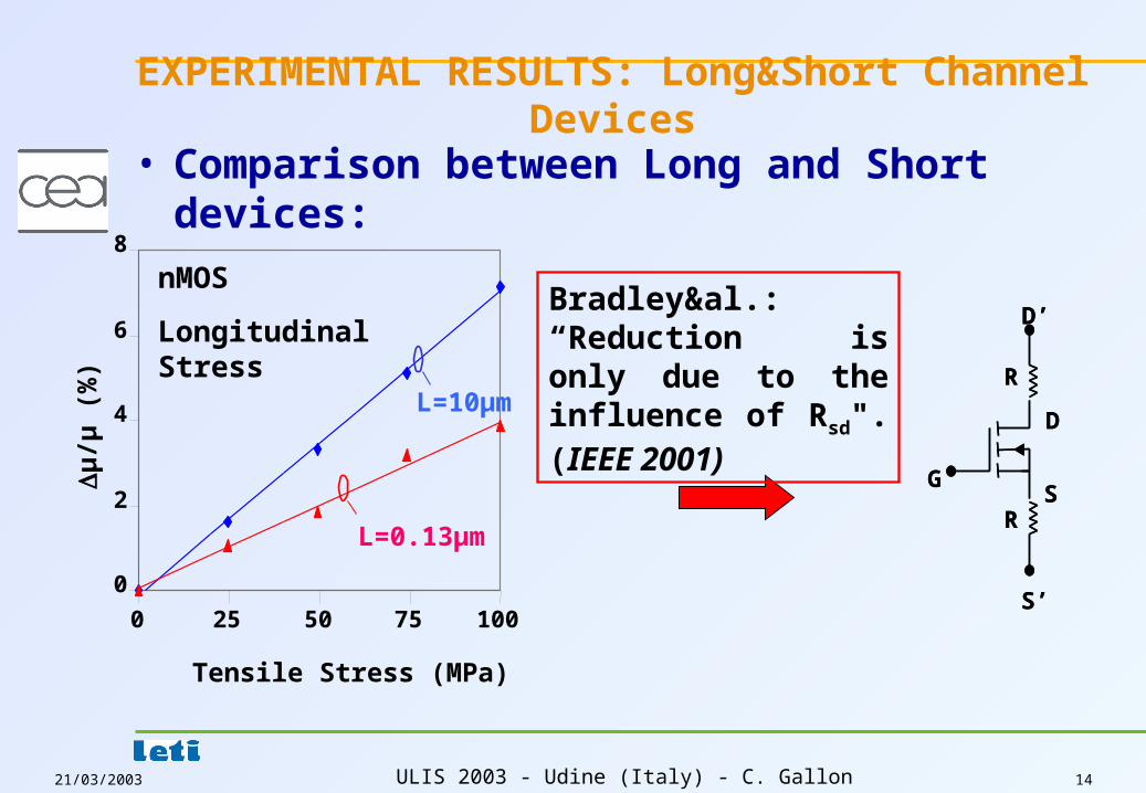
EXPERIMENTAL RESULTS: Long&Short Channel Devices
0
2
4
6
8
0 25 50 75 100
Tensile Stress (MPa)
µ/µ
(%
)
L=0.13µm
L=10µm
nMOS
Longitudinal StressD’
S’
D
S
R
R
G
D’
S’
D
S
R
R
G
• Comparison between Long and Short devices:
Bradley&al.: “Reduction is only due to the influence of Rsd". (IEEE 2001)
21/03/2003 ULIS 2003 - Udine (Italy) - C. Gallon 15
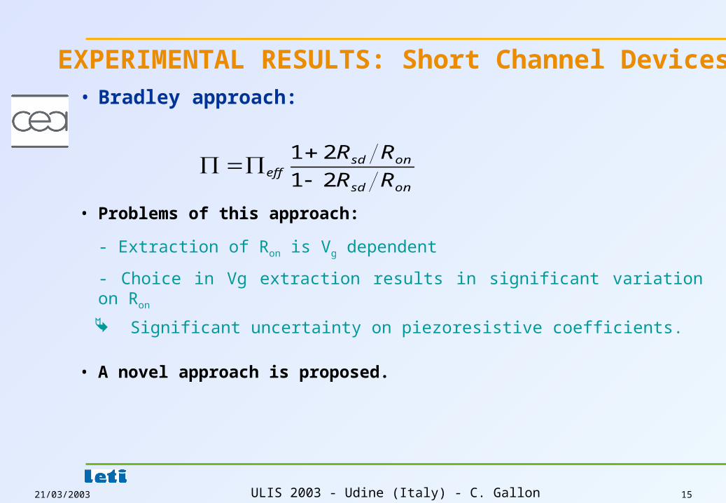
• Bradley approach:
• Problems of this approach:
- Extraction of Ron is Vg dependent
- Choice in Vg extraction results in significant variation on Ron
Significant uncertainty on piezoresistive coefficients.
• A novel approach is proposed.
onsd
onsdeff RR
RR
21
21
EXPERIMENTAL RESULTS: Short Channel Devices

21/03/2003 ULIS 2003 - Udine (Italy) - C. Gallon 16
• New approach proposed:
1. Correction from Rsd influence on Id0:
2. Calculation of equivalent Vg shift to get the same Id with and without stress:
3. Vg is related to Vt and mobility change by:
Vd/IdR1
1IdId
0sd0
Gm/)stressed
Idunstressed
Id(Gm/IdVg
0µ/0µGm
IdVtVg [Roux-dit-Buisson,
IEEProceedings-G, 1993]
EXPERIMENTAL RESULTS: Short Channel Devices
21/03/2003 ULIS 2003 - Udine (Italy) - C. Gallon 17
1. Experimental variations after various stress levels for a 0.13µm pMOS/SOI.
Note excellent linearity.
0 0,1 0,2 0,3 0,4 0,5 0,6
100MPa
75MPa
50MPa
25MPa
0
1
2
3
4
5
0 0,1 0,2 0,3 0,4 0,5 0,6
Vg=
Id
/Gm
(10
-2V
)
Id/Gm (V)
µµSlope /
0 TV
3. Piezoresistive coefficients extraction.
EXPERIMENTAL RESULTS: Short Channel Devices
Longitudinal
Transversal02468
0 25 50 75 100
02468
0 25 50 75 100
No Rsd CorrectionRsd correction
- 2- 4- 6
- 8
Tensile Stress (MPa)µ
/µ (
%)
2. Normalized mobility change versus applied uniaxial stress.

21/03/2003 ULIS 2003 - Udine (Italy) - C. Gallon 18
• Example of calculations including Rsd corrections:
- Agreement between coefficients for both short and long L.
- Local or 2D stress do not affect significantly short devices,however a slight longitudinal effect may exist.
SOI pMOSFET
parameters
Measured values
Measured values
Corrected values
Errors
Channel length 10µm 0.13µm 0.13µm 0.13µm
Parasitic Rsd 35 35 35 35
Vd -0.1V -0.1 V -0.1V -0.1 V
L
T
S
44
-967
531
-435
-1499
-545
473
71
-1018
-708
567
-141
-1275
100
100
150
150
EXPERIMENTAL RESULTS: Short Channel Devices

21/03/2003 ULIS 2003 - Udine (Italy) - C. Gallon 19
CONCLUSIONS & PERSPECTIVES
• Study of mechanical stress effects on long and short channels.
• Proposition of a simple approach to determine directly Vt and µ
– Vt is independent of stress,
– Mobility variations dominate the piezoresistive response,
– Bulk & SOI: similar piezoresistive response both n and p MOS, slightly higher for SOI.
• After Rsd corrections, comparable results on short and long devices:
2D or local effects are small for a 0.13µm technology.
• A first step to provide piezoresistive data for device simulators and a better analysis of mechanical stress effects.
Related Documents