2 IX September 2014

Welcome message from author
This document is posted to help you gain knowledge. Please leave a comment to let me know what you think about it! Share it to your friends and learn new things together.
Transcript

2 IX September 2014
www.ijraset.com Vol. 2 Issue IX, September 2014
ISSN: 2321-9653
I N T E R N A T I O N A L J O U R N A L F O R R E S E A R C H I N A P P L I E D S C I E N C EAN D E N G I N E E R I N G T E C H N O L O G Y (I J R A S E T)
Page 178
Design of Multiplier and Divider Using Reversible Logic Gates with Vedic Mathematical Approach
G.Radhika1, D.R.V.A.Sharath Kumar2
1Department of VLSI and Embedded System, JNTU University
Hyderabad, India2Department of Electronics and communication Engineering
JNTU Hyderabad, India
Abstract---Arithmetic operations are the main components in any design of Digital signal processing or microcontrollers. Multipliers and Divider circuits includes the adders and substations. The main requirements of Digital Signal Processing are High Speed, Low Power and Small Area. To approach these considerations in the designing of Multiplier and Divider Reversibility and Vedic Mathematics approaches are used. The Reversible Logic Gates reduces the Power Dissipation in the Circuit. The Multiplier and Divider are designed by using Reversible logic gates in order to minimize the Power Dissipation of Processors. The Reversible Logic Gates are helps in Quantum Cost Approach. The Speed of the Processor can be improved by reducing the number of multiplications performed per unit time. Hence the system Performance and Efficiency increases. To achieve the requirement the “Urdhva Triyambhayam” concept is introduced. The Urdhva Triyambhayam is taken from the Vedic Mathematics. The proposed Design consists of Multiplier and Divider circuits of Low Power dissipation using Reversible logic gates and High Speed Using Vedic Mathematics. This Design can be applicable in Low Power VLSI and DSP applications, Nano-Technology, Software Defined radios, Cryptography and Wireless Communications. The Design is simulated by using Xilinx 13.2 simulation tool in Verilog Language.Key Words: Reversible Logic Gates, Quantum Cost, Urdhva Triyambhayam, Vedic Mathematics, Verilog code.
NOMENCLATURE:DSP- Digital Signal ProcessingVLSI- Very large scale Integrated CircuitUT- Urdhva TriyambhayamQC- Quantum CostG- Garbage OutputFG- Feynman / CNOT GateFRG- Fredkin gatePG- Peres GateHNG- Haghparast and Navi GateRCA- Ripple Carry AdderMux- Multiplexer
I. INTRODUCTION1. Digital Signal Processing:
A digital signal processor (DSP) is an integrated circuit designed for high-speed data manipulations, and is
used in audio, communications, image manipulation, and other data-acquisition and data-control applications. The arithmetic operations performed by most of the DSPs are addition, subtraction which are simple and multiplication, division are complex. The simple multiplication operation

www.ijraset.com Vol. 2 Issue IX, September 2014
ISSN: 2321-9653
I N T E R N A T I O N A L J O U R N A L F O R R E S E A R C H I N A P P L I E D S C I E N C EAN D E N G I N E E R I N G T E C H N O L O G Y (I J R A S E T)
Page 179
may consume many cycles to complete the operation. This causes the processor to become quite slow. To overcome this problem UT multiplier is used. The main constraints of any embedded system are low Power dissipation, high Speed, less Area [6]. The speed of the processor can be reduced by using the Vedic Mathematics [7]. The minimum power dissipation is one of the main requirements of the system. The power dissipated in the system can be reduced by introducing Reversible logic. The power dissipation of the reversible logicunder idle conditions is Zero [1].
2. Urdhva Triyambhayam Multiplier [7] [10]:To reduce the number of multiplications per unit time
in order to increase the speed/Performance of the system the UT (Urdhva Triyambhayam) multiplier is used. UT Multiplier[10] is an ancient methodology of Indian mathematics as it contains 16 SUTRAS (formulae). A high speed multiplier design by using Urdhva Triyambhayam sutra is proposed. By using this sutra the partial products and sums are generated in one step which reduces the design of architecture in processors. By using this sutra we can reduce the time with high extent when compare to array and booth multiplier. It can be implemented in many (DSP) applications [6] such as convolution, Fast Fourier Transform (FFT) filtering and in microprocessors. By using this method we reduce the propagation delay in comparison with other multipliers.3. Multiplier and Divider:
For division, we use shift/subtract division algorithm. In this algorithm, like multiplication that can be done by repeated additions, the division is done by repeated subtractions [5]. The circuits are designed by using reversible logic gates which is having less heat loss. The multiplier is of high speed with the use of Vedic mathematics. The internal blocks of the multiplier are UT multiplier and Ripple Carry adder implemented by reversible logic gates. The Divider is having less power dissipation with the use of Reversible logic gates. The divider has Multiplexer of 2-bit, shift register of N-bit and Ripple carry adders as the internal blocks. The proposed design is multiplier of 32-bit and divider of N-bit.
4. Reversibility:Reversible logic has shown potential to have
extensive applications in future emerging technologies such as
quantum computing [2][12], optical computing, quantum dot cellular automata as well as ultra low power VLSI circuits, DNA computing to produce zero power dissipation under ideal conditions. Reversible logic is very essential for the construction of low power, low loss computational structures which are very essential for the construction of arithmetic circuits used in quantum computation [17], nanotechnology[18] and other low power digital circuits.
Design that does not result in information loss is called reversible. It naturally takes care of heat generated due to information loss. Bennett showed that zero energy dissipation would be possible only if the network consists of reversible logic gates. Thus reversibility will become an essential property in future circuit design technologies. The outputs can be obtained from the inputs as well as the inputs can be reconstructed by the outputs. This is one of the differences of reversible logic gates compared to normal logic gates [22]. So that there will be less energy loss presents in the circuit.
The paper is partitioned into nine sections. Section II having block diagrams of the proposed design, Section III explains about the Reversibility concept, Section IV is notes on Vedic Mathematics, Section V explains about ripple carry adder , Section VI introduces the shift Register, Section VII gives the operation of blocks in the design, Section VIII shows the output wave forms and Section IX concludes the proposed design and References follows.
II.BLOCK DIAGRAMS
1. Block Diagram of Multiplier:
Fig.1. Block Diagram of 32-Bit Multiplier
www.ijraset.com Vol. 2 Issue IX, September 2014
ISSN: 2321-9653
I N T E R N A T I O N A L J O U R N A L F O R R E S E A R C H I N A P P L I E D S C I E N C EAN D E N G I N E E R I N G T E C H N O L O G Y (I J R A S E T)
Page 180
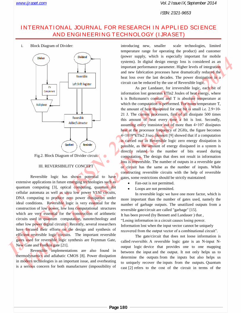
i. Block Diagram of Divider:
Fig.2. Block Diagram of Divider circuit
III. REVERSIBILITY CONCEPT
Reversible logic has shown potential to have extensive applications in future emerging technologies such as quantum computing [3], optical computing, quantum dot cellular automata as well as ultra low power VLSI circuits, DNA computing to produce zero power dissipation under ideal conditions. Reversible logic is very essential for the construction of low power, low loss computational structures which are very essential for the construction of arithmetic circuits used in quantum computation, nanotechnology and other low power digital circuits. Recently, several researchers have focused their efforts on the design and synthesis of efficient reversible logic circuits. The important reversible gates used for reversible logic synthesis are Feynman Gate, New Gate and Fredkin gate [21].
Reversible implementations are also found in thermodynamics and adiabatic CMOS [8]. Power dissipation in modern technologies is an important issue, and overheating is a serious concern for both manufacturer (impossibility of
introducing new, smaller scale technologies, limited temperature range for operating the product) and customer (power supply, which is especially important for mobile systems). In digital design energy loss is considered as an important performance parameter. Higher levels of integration and new fabrication processes have dramatically reduced the heat loss over the last decades. The power dissipation in a circuit can be reduced by the use of Reversible logic.
As per Landauer, for irreversible logic, each bit of information lost generates kTln2 Joules of heat energy, where k is Boltzmann's constant and T is absolute temperature at which the computation is performed. For room temperature T, the amount of heat dissipated for one bit is small i.e. 2.9×10⁻²¹ J. The current processors, first of all dissipate 500 times this amount of heat every time a bit is lost. Secondly, assuming every transistor out of more than 4×10⁷ dissipates heat at the processor frequency of 2GHz, the figure becomes 4×10¹⁹*kTln2 J/sec. Bennett [9] showed that if a computation is carried out in Reversible logic zero energy dissipation is possible, as the amount of energy dissipated in a system is directly related to the number of bits erased during computation. The design that does not result in information loss is irreversible. The number of outputs in a reversible gate or circuit has the same as the number of inputs. While constructing reversible circuits with the help of reversible gates, some restrictions should be strictly maintained:
Fan-out is not permitted.
Loops are not permitted.In reversible logic we have one more factor, which is
more important than the number of gates used, namely the number of garbage outputs. The unutilized outputs from a reversible gate/circuit are called "garbage" [15].It has been proved (by Bennett and Landauer ) that ,“Losing information in a circuit causes losing power. Information lost when the input vector cannot be uniquely recovered from the output vector of a combinational circuit”.
The gate/circuit that does not loose information is called reversible. A reversible logic gate is an N-input N-output logic device that provides one to one mapping between the input and the output. It not only helps us to determine the outputs from the inputs but also helps us to uniquely recover the inputs from the outputs. Quantum cast [2] refers to the cost of the circuit in terms of the

www.ijraset.com
I N T E R N A T I O N A L J O U R NAN D E N G I N E E
cost of a primitive gate. Gate count [10] is the number of reversible gates used to realize the function. Gate level refers to the number of levels which are required to realize the given logic functions. The following are the important design constraints for reversible logic circuits [10]. I. Reversible logic gates do not allow fan-outs. 2. Reversible logic circuits should have minimum QC.3. The design can be optimized so as to produce minimum number of garbage outputs. 4. The reversible logic circuits must use minimum number of constant inputs. 5. The reversible logic circuits must use a minimum logic depth or gate levels. The basic reversible logic gates encountered during the design are listed below: 1. Feynman Gate [21]:
It is a 2x2 gate and its logic circuit is as shown in the figure. It is also known as Controlled Not (CNOT) Gate. It has quantum cost one and is generally used for Fan Out purposes.
Fig.3. Feynman gate2. Peres Gate [11]:
It is a 3x3 gate and its logic circuit is as shown in the figure. It has quantum cost four. It is used to realize various Boolean functions such as AND, XOR.
Fig.4. Peres gate
Vol. 2 Issue I
ISSN: 2321-9
N A L F O R R E S E A R C H I N A P P L I EE R I N G T E C H N O L O G Y (I J R A S E T
is the number of reversible gates used to realize the function. Gate level
number of levels which are required to
The following are the important design constraints for
outs. hould have minimum QC.
3. The design can be optimized so as to produce minimum
4. The reversible logic circuits must use minimum number of
5. The reversible logic circuits must use a minimum logic
The basic reversible logic gates encountered during the design
It is a 2x2 gate and its logic circuit is as shown in the figure. It is also known as Controlled Not (CNOT) Gate. It
and is generally used for Fan Out
It is a 3x3 gate and its logic circuit is as shown in the figure. It has quantum cost four. It is used to realize various Boolean functions such as AND, XOR.
3. Fredkin Gate [21]: It is a 3x3 gate and its logic circuit is as shown
in the figure. It has quantum cost five. It can be used to implement a Multiplexer.
Fig.5. Fredkin gate4. HNG Gate [14][16]:
It is a 4x4 gate and its logic circuit is as shown in the figure. It has quantum cost six. It is used for designing ripple carry adders. It can produce both sum and carry in a single gate thus minimizing the garbage and gate counts.
Fig.6. HNG gate
IV.VEDIC MULTIPLICATION
The use of Vedic mathematics typical calculations in conventional mathematics to very simple one. Because the Vedic formulae are claimed to be based on the natural principles on which the human mind works. Vedic Mathematics is a methodology of arithmetic rules that allow more efficient speed implementation. It also provides some effective algorithms which can be applied to various branches of engineering such as computing.1. Urdhva Triyambhayam Sutra:
Higher throughput arithmetic operations are important to achieve the desired performance in many realtime signal and image processing applications. One of the key
IX, September 2014
9653
E D S C I E N C ET)
It is a 3x3 gate and its logic circuit is as shown in the figure. It has quantum cost five. It can be used to
Fig.5. Fredkin gate
It is a 4x4 gate and its logic circuit is as shown in the gure. It has quantum cost six. It is used for designing ripple
carry adders. It can produce both sum and carry in a single gate thus minimizing the garbage and gate counts.
Fig.6. HNG gate
IV.VEDIC MULTIPLICATION
The use of Vedic mathematics [7] is to reduce the typical calculations in conventional mathematics to very simple one. Because the Vedic formulae are claimed to be based on the natural principles on which the human mind works. Vedic Mathematics is a methodology of arithmetic
more efficient speed implementation. It also provides some effective algorithms which can be applied to various branches of engineering such as computing.
Higher throughput arithmetic operations are important to achieve the desired performance in many real-time signal and image processing applications. One of the key

www.ijraset.com
I N T E R N A T I O N A L J O U R NAN D E N G I N E E
arithmetic operations in such applications [6] is multiplication and the development of fast multiplier circuit has been a subject of interest over decades. Reducing the time delay and power consumption are very essential requirements for many applications.
Multiplication is an fundamental function in arithmetic operations based on this operatioMultiply and Accumulate(MAC) in many Digital Signal Processing(DSP) applications such as convolution, Fast Fourier Transform(FFT), filtering and in microprocessors in its arithmetic and logic unit. Since multiplication dominates the execution time of most DSP algorithms, so there is a need of high speed multiplier. Currently, multiplication time is still the dominant factor in determining the instruction cycle time of a DSP chip. The demand for high speed processing has been increasing as a result of expanding computer and signal processing applications.
The proposed Vedic multiplier is based on the “Urdhva Triyambhayam” sutra (algorithm) [7]have been traditionally used for the multiplication of two numbers in the decimal number system. In this work, we apply the same ideas to the binary number system to make the proposed algorithm compatible with the digital hardware. It is a general multiplication formula applicable to all cases of multiplication. It literally means “Vertically and[10]. The basic UT multiplier is of 2-bit. The proposed system is having 32-bit UT multipliers which are obtained from the basic UT Multiplier of 2*2. The multiplier consists of UT multipliers and adders. The adders that are used are Ripple Carry Adders (RCA) [13]. The RCA are the adders which takes the input carry of present adder from the output carry of the previous adder. The UT multiplier can be designed for large number of bits also which may be decimal or binary numbers. The example for two bit using binary multiplication is shown in Fig.7. The process is done in 3 steps. First step: The last significant bits (LSB) vertical multiplication and adding with previous carry (initially 0),Second step: The cross wise multiplication of the LSB significant bit) and MSB (most significant bit) and adding with the previous carry andThird step: The vertical multiplication of MSB (most significant bit) and adding with the previous carry.The resultant vector consists of LSB bits of individual r
Vol. 2 Issue I
ISSN: 2321-9
N A L F O R R E S E A R C H I N A P P L I EE R I N G T E C H N O L O G Y (I J R A S E T
is multiplication multiplier circuit has been a
subject of interest over decades. Reducing the time delay and power consumption are very essential requirements for many
Multiplication is an fundamental function in arithmetic operations based on this operations such as Multiply and Accumulate(MAC) in many Digital Signal Processing(DSP) applications such as convolution, Fast Fourier Transform(FFT), filtering and in microprocessors in its arithmetic and logic unit. Since multiplication dominates
me of most DSP algorithms, so there is a need of high speed multiplier. Currently, multiplication time is still the dominant factor in determining the instruction cycle time of a DSP chip. The demand for high speed processing has
t of expanding computer and signal
The proposed Vedic multiplier is based on the [7]. These Sutras
have been traditionally used for the multiplication of two tem. In this work, we
apply the same ideas to the binary number system to make the proposed algorithm compatible with the digital hardware. It is a general multiplication formula applicable to all cases of
Vertically and Cross wise”bit. The proposed system
bit UT multipliers which are obtained from the basic UT Multiplier of 2*2. The multiplier consists of UT multipliers and adders. The adders that are used are Ripple
. The RCA are the adders which takes the input carry of present adder from the output carry of the previous adder. The UT multiplier can be designed for large number of bits also which may be decimal or binary
two bit using binary multiplication The process is done in 3 steps.
First step: The last significant bits (LSB) vertical multiplication and adding with previous carry (initially 0),Second step: The cross wise multiplication of the LSB (last significant bit) and MSB (most significant bit) and adding
Third step: The vertical multiplication of MSB (most significant bit) and adding with the previous carry.The resultant vector consists of LSB bits of individual results
and MSB bits are stored in the carry.
Fig.7. 2*2 bit binary number UT multiplication
The normal UT multiplier consists of logic gates XOR, AND gates for which the fan out is more. The block diagram of the UT multiplier of 2-bit is shown in theusing the reversible logic gates the block diagram of UT Multiplier is shown in fig.9. The circuit consists of Peres gates and Feynman gate which requires quantum cost of 21, less than the design with normal gates.
Fig.8. UT multiplier block diagram using normal logic gates
IX, September 2014
9653
E D S C I E N C ET)
Fig.7. 2*2 bit binary number UT multiplication
The normal UT multiplier consists of logic gates XOR, AND gates for which the fan out is more. The block
bit is shown in the fig.8. By using the reversible logic gates the block diagram of UT
. The circuit consists of Peres gates and Feynman gate which requires quantum cost of 21, less
diagram using normal logic gates

www.ijraset.com Vol. 2 Issue IX, September 2014
ISSN: 2321-9653
I N T E R N A T I O N A L J O U R N A L F O R R E S E A R C H I N A P P L I E D S C I E N C EAN D E N G I N E E R I N G T E C H N O L O G Y (I J R A S E T)
Page 183
Fig.9. UT multiplier block diagram using reversible logic gates
The design of 32- bit multiplier requires 16- bit multiplier where as 16-bit multiplier requires 8-bit multiplier, 8-bit requires 4-bit and the 4-bit multiplier requires 2- bit UT multiplier. The 4*4 multiplier is the existing system of multiplier design using reversible logic concept. The block diagram of the 4*4 multiplier is shown in the figure.10. It consists of four 2X2 multipliers each of which produces four bits as inputs; two bits from the multiplicand and two bits from the multiplier. The lower two bits of the output of the first 2X2 multiplier are entrapped as the lowest two bits of the final result of multiplication. The addition is done by a five bit ripple carry adder which generates a six bit output. The ripple carry adder is consummated (realized) using the HNG Gate. A 4 bit ripple carry adder needs 4 HNG gates and the 5 bit adder requires 5 HNG gates. This design also does not take into consideration the fan out gates.
Fig.10. 4*4 UT multiplier block diagram
V.RIPPLE CARRY ADDER
A ripple carry adder is a digital circuit that produces the arithmetic sum of two binary numbers. It can be constructed with full adders connected in cascaded with the carry output from each full adder connected to the carry input of the next full adder in the chain. The ripple carry adder is designed by using the reversible logic gates. The full adder circuit is replaced by the HNG gate for which the multiplier and multiplicand carry and zero bits are the inputs to produce the outputs as Sum and Carry. For this design the quantum cost is computed to be 162, the total number of gates used will be 37, the number of garbage outputs will be 62 and the number of constant inputs will be 29.
Fig.11. Ripple Carry Adder using HNG gates
www.ijraset.com Vol. 2 Issue IX, September 2014
ISSN: 2321-9653
I N T E R N A T I O N A L J O U R N A L F O R R E S E A R C H I N A P P L I E D S C I E N C EAN D E N G I N E E R I N G T E C H N O L O G Y (I J R A S E T)
Page 184
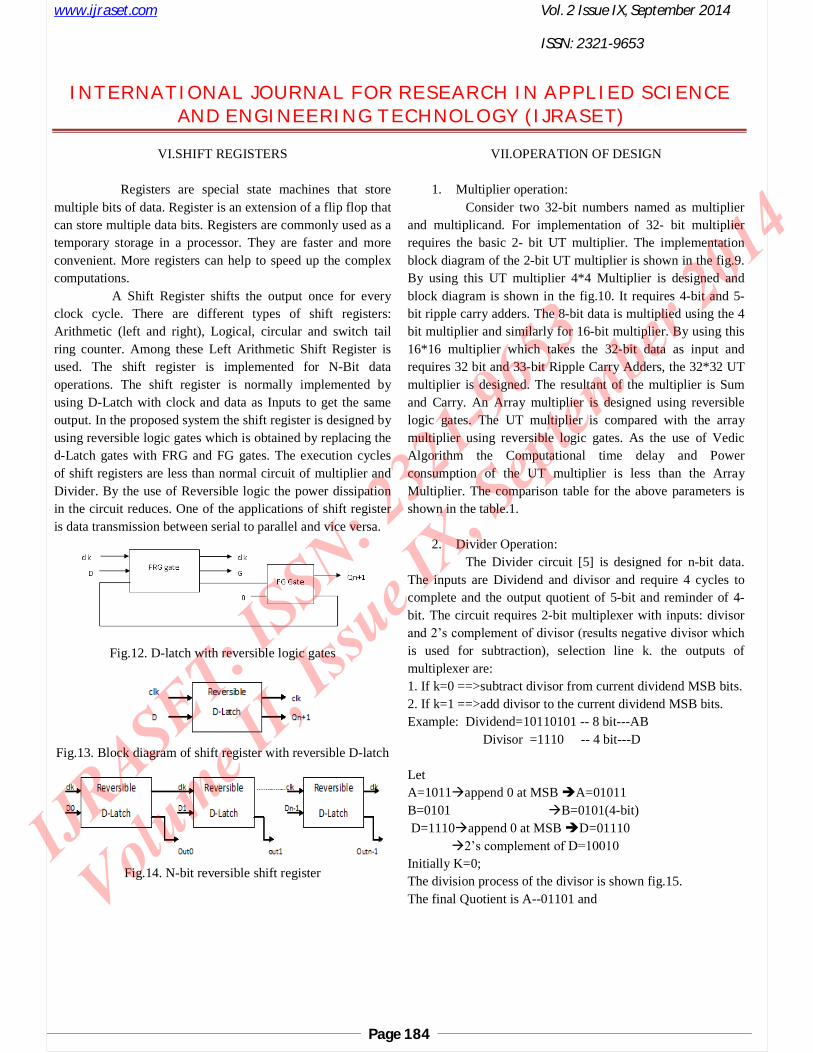
VI.SHIFT REGISTERS
Registers are special state machines that store multiple bits of data. Register is an extension of a flip flop that can store multiple data bits. Registers are commonly used as a temporary storage in a processor. They are faster and more convenient. More registers can help to speed up the complex computations.
A Shift Register shifts the output once for every clock cycle. There are different types of shift registers: Arithmetic (left and right), Logical, circular and switch tail ring counter. Among these Left Arithmetic Shift Register is used. The shift register is implemented for N-Bit data operations. The shift register is normally implemented by using D-Latch with clock and data as Inputs to get the same output. In the proposed system the shift register is designed by using reversible logic gates which is obtained by replacing the d-Latch gates with FRG and FG gates. The execution cycles of shift registers are less than normal circuit of multiplier and Divider. By the use of Reversible logic the power dissipation in the circuit reduces. One of the applications of shift register is data transmission between serial to parallel and vice versa.
Fig.12. D-latch with reversible logic gates
Fig.13. Block diagram of shift register with reversible D-latch
Fig.14. N-bit reversible shift register
VII.OPERATION OF DESIGN
1. Multiplier operation:Consider two 32-bit numbers named as multiplier
and multiplicand. For implementation of 32- bit multiplier requires the basic 2- bit UT multiplier. The implementation block diagram of the 2-bit UT multiplier is shown in the fig.9. By using this UT multiplier 4*4 Multiplier is designed and block diagram is shown in the fig.10. It requires 4-bit and 5-bit ripple carry adders. The 8-bit data is multiplied using the 4 bit multiplier and similarly for 16-bit multiplier. By using this 16*16 multiplier which takes the 32-bit data as input and requires 32 bit and 33-bit Ripple Carry Adders, the 32*32 UT multiplier is designed. The resultant of the multiplier is Sum and Carry. An Array multiplier is designed using reversible logic gates. The UT multiplier is compared with the array multiplier using reversible logic gates. As the use of Vedic Algorithm the Computational time delay and Power consumption of the UT multiplier is less than the Array Multiplier. The comparison table for the above parameters is shown in the table.1.
2. Divider Operation:The Divider circuit [5] is designed for n-bit data.
The inputs are Dividend and divisor and require 4 cycles to complete and the output quotient of 5-bit and reminder of 4-bit. The circuit requires 2-bit multiplexer with inputs: divisor and 2’s complement of divisor (results negative divisor which is used for subtraction), selection line k. the outputs of multiplexer are:1. If k=0 ==>subtract divisor from current dividend MSB bits.2. If k=1 ==>add divisor to the current dividend MSB bits.Example: Dividend=10110101 -- 8 bit---AB
Divisor =1110 -- 4 bit---D
Let A=1011append 0 at MSB A=01011B=0101 B=0101(4-bit)D=1110append 0 at MSB D=01110
2’s complement of D=10010Initially K=0;The division process of the divisor is shown fig.15.The final Quotient is A--01101 and

www.ijraset.com Vol. 2 Issue IX, September 2014
ISSN: 2321-9653
I N T E R N A T I O N A L J O U R N A L F O R R E S E A R C H I N A P P L I E D S C I E N C EAN D E N G I N E E R I N G T E C H N O L O G Y (I J R A S E T)
Page 185
The final reminder is B—1100
Z K A(5-bit) B(4-bit)
X 01011 0101
Left Shift 0 10110 101-
subtract 10010 CYCLE-1
Insert invert of MSB to LSB
1(discard) 01000 1011
01000 1011
Left shift 0 1000 011-
subtract 10010 CYCLE-2
Insert invert of MSB to LSB
1(discard) 00011 0111
00011 0111
Left Shift 0 00110 111-
Subtract 10010 CYCLE-3
Insert invert of MSB to LSB
0(discard) 11000 1110
11000 1110
Left Shift 1 10001 110-add 01110 CYCLE-4
Insert invert of MSB to LSB
- 11111 1100
11111 1100Restoration of final
reminder and quotientadd 01110
1(discard) 01101 1100
Fig.15. Example of Division Operation

www.ijraset.com
I N T E R N A T I O N A L J O U R NAN D E N G I N E E
VIII.SIMULATION
The design is coded in Verilog language. The simulation tool used is Xilinx ISE 13.2 version. For synthesize or execution FPGA – Spartan 3E family is used. The multiplier is compared with the array multiplierthe power consumption and speed are more the UT multiplier. The comparison table for UT multiplier, Array Multiplier and Divider circuit are shown below table.
Table.1. Comparison table of array multiplier and proposed system
Parameter
Array Multiplier
UT Multiplie
r
Divider
Operation Speed
Less More
Maximum Path Delay
126.335ns 87.587ns 37.130ns
Dynamic Power
3.42 mW 0.03mW 0.81mW
FPGA Implementation
Less efficient
More efficient efficient
THE OUTPUT WAVE FORMS:The output wave form of multiplier for the example of 32input and the output is of 64-bit.
Fig.16. Multiplier output wave form
Vol. 2 Issue I
ISSN: 2321-9
N A L F O R R E S E A R C H I N A P P L I EE R I N G T E C H N O L O G Y (I J R A S E T
is coded in Verilog language. The simulation tool used is Xilinx ISE 13.2 version. For synthesize
Spartan 3E family is used. The multiplier is compared with the array multiplier [15] for which
e UT multiplier. The comparison table for UT multiplier, Array Multiplier and
Table.1. Comparison table of array multiplier and proposed
Divider
More
37.130ns
0.81mW
More efficient
The output wave form of multiplier for the example of 32- bit
Fig.16. Multiplier output wave form
The output wave form of Divider for the example of 8dividend and 4- bit divisor and the outputs are 5and 4-bit Reminder.
Fig.17. Divider circuit output waveforms
IX.CONCLUSION
In this paper the multiplier and divider circuits are designed. To satisfy some of the Digital signal processing considerations like Low Power dissipation, High Speed/Performance we have implemented these arithmetic blocks. This proposed paper implemented for Reversible Vedic Multiplier [16] using Urdhva Triyambhayam sutra[7][10] and Reversible Divider circuitderived from Vedic Mathematics results to the fast multiplication which improves the speed of the processor. Hence the efficiency of the system also increases. To reduce the power dissipation of the design the reversible logic gates are used for implantation of the circuit. The reversible logic gate dissipates zero power ideally.The existing system is of 4- bit multiplier design and Divider circuit of Irreversible logic gates [20]. The proposed system is of 32- bit multiplier design and Divider circuit of Reversible logic gates. The proposed design is having better quantum cost compared to existing designs. Trough thhaving more garbage outputs they can be used as fan outs for other gates. The Dynamic power and the speed delay of the UT multiplier and Divider are compared with the array multiplier design. The Vedic mathematics is used for large number of bit Multiplications as well as Division Process. The
IX, September 2014
9653
E D S C I E N C ET)
The output wave form of Divider for the example of 8-bit bit divisor and the outputs are 5-bit Quotient
Fig.17. Divider circuit output waveforms
CONCLUSION
In this paper the multiplier and divider circuits are designed. To satisfy some of the Digital signal processing considerations like Low Power dissipation, High Speed/Performance we have implemented these arithmetic
implemented for Reversible using Urdhva Triyambhayam sutra
and Reversible Divider circuit [5]. The UT multiplier derived from Vedic Mathematics results to the fast multiplication which improves the speed of the processor.
e the efficiency of the system also increases. To reduce the power dissipation of the design the reversible logic gates are used for implantation of the circuit. The reversible logic
iplier design and Divider . The proposed system is
bit multiplier design and Divider circuit of Reversible logic gates. The proposed design is having better quantum cost compared to existing designs. Trough the design is having more garbage outputs they can be used as fan outs for other gates. The Dynamic power and the speed delay of the UT multiplier and Divider are compared with the array multiplier design. The Vedic mathematics is used for large
t Multiplications as well as Division Process. The

www.ijraset.com Vol. 2 Issue IX, September 2014
ISSN: 2321-9653
I N T E R N A T I O N A L J O U R N A L F O R R E S E A R C H I N A P P L I E D S C I E N C EAN D E N G I N E E R I N G T E C H N O L O G Y (I J R A S E T)
Page 187
proposed design can be used for the applications like Low power DSP applications, High Speed operations for Filters, Transformations, wireless and radio communications Nano technology, Cryptography [6][18][4].
REFERENCES
[1]. Perkowski, M., A. Al-Rabadi, P. Kerntopf, A. Buller, M. Chrzanowska-Jeske, A. Mishchenko, M.A. Khan, A. Coppola, S. Yanushkevich, V. Shmerko and L. Jozwiak, 2001. A general decomposition for reversible logic. Proc. RM, Starkville, pp: 119-138.
[2]. Peres,A.,1985.Reversible logic and quantum computers. Phy. Rev., 32: 3266-3276.
[3]. Toffoli, T., 1980. Reversible computing. Tech Memo MIT/LCS/TM-151. MIT Lab for Computer Science
[4]. Thapliyal, H. and M. Zwolinski, 2006. Reversible Logic to Cryptographic Hardware: A New Paradigm., 49th IEEE International Midwest Symposium on Circuits and Systems.
[5]. Nayeem, N.M., A. Md. H. Md, M. Haque, L. Jamal and H.M.H. Babu, 2009., Novel Reversible Division Hardware. IEEE International Midwest Symposium on Circuits and Systems, pp: 1134-1138.
[6]. Parhami B., 2000. Computer Arithmetic: Algorithms and Hardware Designs. Oxford University Press, New York.
[7]. Swami Bharati Krsna Tirtha, Vedic Mathematics. Delhi: Motilal Banarsidass publishers 1965.
[8]. Rakshith Saligram and Rakshith T.R. "Design of Reversible Multipliers for linear filtering Applications in DSP" International Journal of VLSI Design and Communication systems, Dec-12.
[9]. C.H. Bennett, "Logical reversibility of Computation", IBM J. Research and Development, pp.525-532, November 1973.
[10]. G Ganesh Kumarand V Charishma, Design of high speed vedic multiplier using vedic mathematics techniques, ltn'l J. of Scientific and Research Publications, Vol. 2 Issue 3 March 2012
[11]. A. Peres,Reversible logic and quantum computers,Phys.Rev.A32 (1985) 3266-3276.
[12]. M S Islam, M M Rahman, Z Begum and M Z
Hafiz, 2009. Low Cost Quantum Realization of Reversible Multiplier Circuit. Information Technology Journal, vol. 8(2), pp. 208-213.
[13]. M. S. Islam et al. , "Realization of Reversible Multiplier Circuit," in Information Tech. 1, Vol. 8, No. 2, pp. 117-121, 2005.
[14]. K.Navi.M.Haghparast, S.JafaraliJassbi, HashemiPour, design of Novel Reversible Multiplier using HNG gate, World Sci,13(6).
[15]. Thapliyal, H., M.B. Srinivas and H.R. Arabnia, 2005, A Reversible Version of 4x4 Bit Array Multiplier with Minimum Gates and Garbage Outputs, Int. Conf. Embedded System, Applications (ESA'05), Las Vegas, USA, pp: 106 114.
[16]. H. Thapliyal and M.B. Srinivas, "Reversible Multiplier Architecture Using TSG Gate", Proc. IEEE International Conference on Computer Systems and Applications, pp. 241-244, March-07.
[17]. R. Feynman, "Quantum Mechanical Computers," Optics News,Vol.1l, pp. 11-20, 1985.
[18]. Shams, M., M. Haghparast and K. Navi, Novel reversible multiplier circuit in nanotechnology. World Appl. Sci. J., 3(5): 806-810
[19]. Somayeh Babazadeh and Majid Haghparast, "Design of a Nanometric Fault Tolerant Reversible Multiplier Circuit" Journal of Basic and Applied Scientific Research, 2012.
[20]. R.landauer,”Irreversibility and heat generation in the computational Process", IBM Research andDevelopment, pp. 183-191, 1961.
[21]. Pallav Gupta, Abhinav Agarwal, and Niraj K.Jha “An Algorithm for Synthesis of Reversible Logic Circuits”, IEEE transactions on computer Aided Design of Integrated circuits and Systems, vol.25, 2006
[22]. B.Raghukanth,Muralikrishna, “A Distinguish Between Reversible and Conventinal Logic Gates”, international Journal of Engineering Reserch and Applications, vol.2,pp 198-151,March-2012.

Related Documents