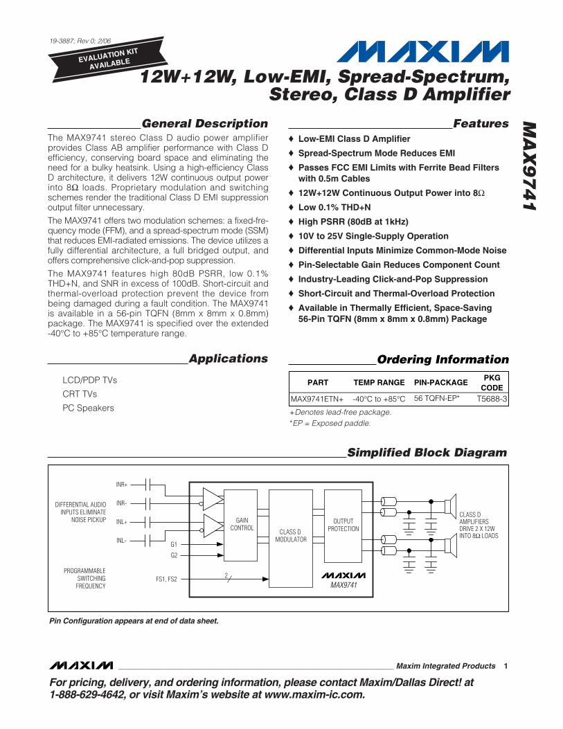
General Description The MAX9741 stereo Class D audio power amplifier provides Class AB amplifier performance with Class D efficiency, conserving board space and eliminating the need for a bulky heatsink. Using a high-efficiency Class D architecture, it delivers 12W continuous output power into 8Ω loads. Proprietary modulation and switching schemes render the traditional Class D EMI suppression output filter unnecessary. The MAX9741 offers two modulation schemes: a fixed-fre- quency mode (FFM), and a spread-spectrum mode (SSM) that reduces EMI-radiated emissions. The device utilizes a fully differential architecture, a full bridged output, and offers comprehensive click-and-pop suppression. The MAX9741 features high 80dB PSRR, low 0.1% THD+N, and SNR in excess of 100dB. Short-circuit and thermal-overload protection prevent the device from being damaged during a fault condition. The MAX9741 is available in a 56-pin TQFN (8mm x 8mm x 0.8mm) package. The MAX9741 is specified over the extended -40°C to +85°C temperature range. Applications Features ♦ Low-EMI Class D Amplifier ♦ Spread-Spectrum Mode Reduces EMI ♦ Passes FCC EMI Limits with Ferrite Bead Filters with 0.5m Cables ♦ 12W+12W Continuous Output Power into 8Ω ♦ Low 0.1% THD+N ♦ High PSRR (80dB at 1kHz) ♦ 10V to 25V Single-Supply Operation ♦ Differential Inputs Minimize Common-Mode Noise ♦ Pin-Selectable Gain Reduces Component Count ♦ Industry-Leading Click-and-Pop Suppression ♦ Short-Circuit and Thermal-Overload Protection ♦ Available in Thermally Efficient, Space-Saving 56-Pin TQFN (8mm x 8mm x 0.8mm) Package MAX9741 12W+12W, Low-EMI, Spread-Spectrum, Stereo, Class D Amplifier ________________________________________________________________ Maxim Integrated Products 1 19-3887; Rev 0; 2/06 For pricing, delivery, and ordering information, please contact Maxim/Dallas Direct! at 1-888-629-4642, or visit Maxim’s website at www.maxim-ic.com. EVALUATION KIT AVAILABLE Ordering Information PART TEMP RANGE PIN-PACKAGE PKG CODE MAX9741ETN+ -40°C to +85°C 56 TQFN-EP* T5688-3 +Denotes lead-free package. *EP = Exposed paddle. LCD/PDP TVs CRT TVs PC Speakers Pin Configuration appears at end of data sheet. CLASS D AMPLIFIERS DRIVE 2 X 12W INTO 8Ω LOADS GAIN CONTROL INR+ DIFFERENTIAL AUDIO INPUTS ELIMINATE NOISE PICKUP PROGRAMMABLE SWITCHING FREQUENCY INR- INL+ INL- FS1, FS2 G2 G1 2 CLASS D MODULATOR OUTPUT PROTECTION MAX9741 Simplified Block Diagram

Welcome message from author
This document is posted to help you gain knowledge. Please leave a comment to let me know what you think about it! Share it to your friends and learn new things together.
Transcript
General DescriptionThe MAX9741 stereo Class D audio power amplifierprovides Class AB amplifier performance with Class Defficiency, conserving board space and eliminating theneed for a bulky heatsink. Using a high-efficiency ClassD architecture, it delivers 12W continuous output powerinto 8Ω loads. Proprietary modulation and switchingschemes render the traditional Class D EMI suppressionoutput filter unnecessary.
The MAX9741 offers two modulation schemes: a fixed-fre-quency mode (FFM), and a spread-spectrum mode (SSM)that reduces EMI-radiated emissions. The device utilizes afully differential architecture, a full bridged output, andoffers comprehensive click-and-pop suppression.
The MAX9741 features high 80dB PSRR, low 0.1%THD+N, and SNR in excess of 100dB. Short-circuit andthermal-overload protection prevent the device frombeing damaged during a fault condition. The MAX9741is available in a 56-pin TQFN (8mm x 8mm x 0.8mm)package. The MAX9741 is specified over the extended-40°C to +85°C temperature range.
Applications
Features♦ Low-EMI Class D Amplifier
♦ Spread-Spectrum Mode Reduces EMI
♦ Passes FCC EMI Limits with Ferrite Bead Filterswith 0.5m Cables
♦ 12W+12W Continuous Output Power into 8Ω♦ Low 0.1% THD+N
♦ High PSRR (80dB at 1kHz)
♦ 10V to 25V Single-Supply Operation
♦ Differential Inputs Minimize Common-Mode Noise
♦ Pin-Selectable Gain Reduces Component Count
♦ Industry-Leading Click-and-Pop Suppression
♦ Short-Circuit and Thermal-Overload Protection
♦ Available in Thermally Efficient, Space-Saving 56-Pin TQFN (8mm x 8mm x 0.8mm) Package
MA
X9
74
1
12W+12W, Low-EMI, Spread-Spectrum, Stereo, Class D Amplifier
________________________________________________________________ Maxim Integrated Products 1
19-3887; Rev 0; 2/06
For pricing, delivery, and ordering information, please contact Maxim/Dallas Direct! at 1-888-629-4642, or visit Maxim’s website at www.maxim-ic.com.
EVALUATION KIT
AVAILABLE
Ordering Information
PART TEMP RANGE PIN-PACKAGEPKG
CODEMAX9741ETN+ -40°C to +85°C 56 TQFN-EP* T5688-3
+Denotes lead-free package.*EP = Exposed paddle.
LCD/PDP TVs
CRT TVs
PC Speakers
Pin Configuration appears at end of data sheet.
CLASS DAMPLIFIERSDRIVE 2 X 12WINTO 8Ω LOADS
GAINCONTROL
INR+
DIFFERENTIAL AUDIOINPUTS ELIMINATE
NOISE PICKUP
PROGRAMMABLESWITCHINGFREQUENCY
INR-
INL+
INL-
FS1, FS2
G2
G1
2
CLASS D MODULATOR
OUTPUTPROTECTION
MAX9741
Simplified Block Diagram
MA
X9
74
1
12W+12W, Low-EMI, Spread-Spectrum, Stereo, Class D Amplifier
2 _______________________________________________________________________________________
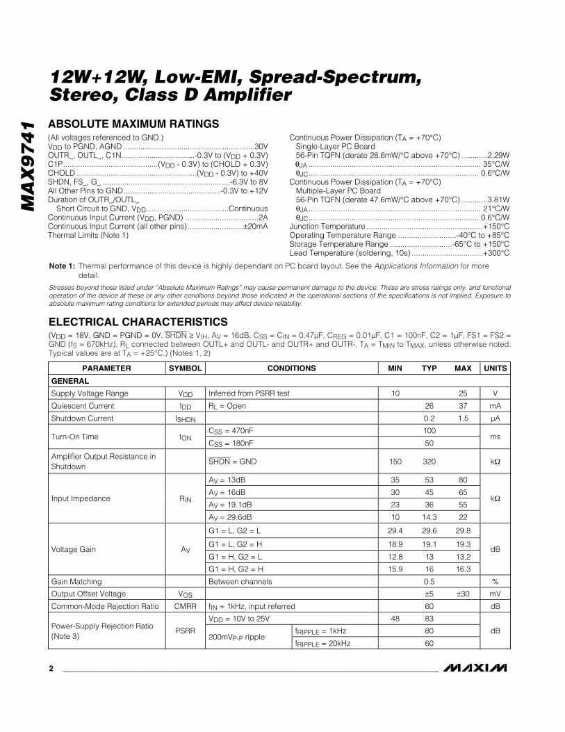
ABSOLUTE MAXIMUM RATINGS
Stresses beyond those listed under “Absolute Maximum Ratings” may cause permanent damage to the device. These are stress ratings only, and functionaloperation of the device at these or any other conditions beyond those indicated in the operational sections of the specifications is not implied. Exposure toabsolute maximum rating conditions for extended periods may affect device reliability.
(All voltages referenced to GND.)VDD to PGND, AGND .............................................................30VOUTR_, OUTL_, C1N..................................-0.3V to (VDD + 0.3V)C1P............................................(VDD - 0.3V) to (CHOLD + 0.3V)CHOLD........................................................(VDD - 0.3V) to +40VSHDN, FS_, G_ ...........................................................-6.3V to 8VAll Other Pins to GND.............................................-0.3V to +12VDuration of OUTR_/OUTL_
Short Circuit to GND, VDD......................................ContinuousContinuous Input Current (VDD, PGND) ..................................2AContinuous Input Current (all other pins)..........................±20mAThermal Limits (Note 1)
Continuous Power Dissipation (TA = +70°C)Single-Layer PC Board56-Pin TQFN (derate 28.6mW/°C above +70°C) ............2.29WθJA ................................................................................ 35°C/WθJC............................................................................... 0.6°C/W
Continuous Power Dissipation (TA = +70°C) Multiple-Layer PC Board56-Pin TQFN (derate 47.6mW/°C above +70°C) ............3.81WθJA................................................................................ 21°C/WθJC............................................................................... 0.6°C/W
Junction Temperature ......................................................+150°COperating Temperature Range ...........................-40°C to +85°CStorage Temperature Range .............................-65°C to +150°CLead Temperature (soldering, 10s) .................................+300°C
ELECTRICAL CHARACTERISTICS(VDD = 18V, GND = PGND = 0V, SHDN ≥ VIH, AV = 16dB, CSS = CIN = 0.47µF, CREG = 0.01µF, C1 = 100nF, C2 = 1µF, FS1 = FS2 =GND (fS = 670kHz), RL connected between OUTL+ and OUTL- and OUTR+ and OUTR-, TA = TMIN to TMAX, unless otherwise noted.Typical values are at TA = +25°C.) (Notes 1, 2)
PARAMETER SYMBOL CONDITIONS MIN TYP MAX UNITS
GENERAL
Supply Voltage Range VDD Inferred from PSRR test 10 25 V
Quiescent Current IDD RL = Open 26 37 mA
Shutdown Current ISHDN 0.2 1.5 µA
CSS = 470nF 100Turn-On Time tON
CSS = 180nF 50ms
Amplifier Output Resistance inShutdown
SHDN = GND 150 320 kΩ
AV = 13dB 35 53 80
AV = 16dB 30 45 65
AV = 19.1dB 23 36 55Input Impedance RIN
AV = 29.6dB 10 14.3 22
kΩ
G1 = L, G2 = L 29.4 29.6 29.8
G1 = L, G2 = H 18.9 19.1 19.3
G1 = H, G2 = L 12.8 13 13.2Voltage Gain AV
G1 = H, G2 = H 15.9 16 16.3
dB
Gain Matching Between channels 0.5 %
Output Offset Voltage VOS ±5 ±30 mV
Common-Mode Rejection Ratio CMRR fIN = 1kHz, input referred 60 dB
VDD = 10V to 25V 48 83
fRIPPLE = 1kHz 80Power-Supply Rejection Ratio(Note 3)
PSRR200mVP-P ripple
fRIPPLE = 20kHz 60
dB
Note 1: Thermal performance of this device is highly dependant on PC board layout. See the Applications Information for moredetail.
MA
X9
74
1
12W+12W, Low-EMI, Spread-Spectrum, Stereo, Class D Amplifier
_______________________________________________________________________________________ 3
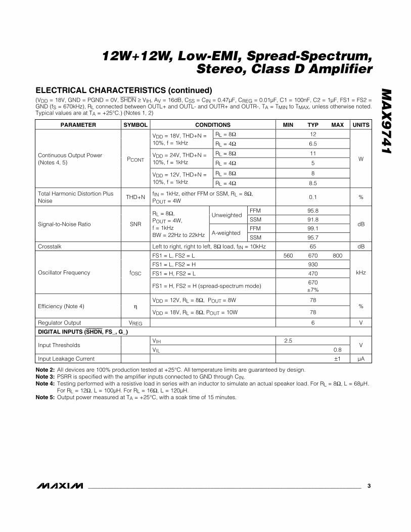
ELECTRICAL CHARACTERISTICS (continued)(VDD = 18V, GND = PGND = 0V, SHDN ≥ VIH, AV = 16dB, CSS = CIN = 0.47µF, CREG = 0.01µF, C1 = 100nF, C2 = 1µF, FS1 = FS2 =GND (fS = 670kHz), RL connected between OUTL+ and OUTL- and OUTR+ and OUTR-, TA = TMIN to TMAX, unless otherwise noted.Typical values are at TA = +25°C.) (Notes 1, 2)
PARAMETER SYMBOL CONDITIONS MIN TYP MAX UNITS
RL = 8Ω 12VDD = 18V, THD+N =10%, f = 1kHz RL = 4Ω 6.5
RL = 8Ω 11VDD = 24V, THD+N =10%, f = 1kHz RL = 4Ω 5
RL = 8Ω 8
Continuous Output Power(Notes 4, 5)
PCONT
VDD = 12V, THD+N =10%, f = 1kHz RL = 4Ω 8.5
W
Total Harmonic Distortion PlusNoise
THD+NfIN = 1kHz, either FFM or SSM, RL = 8Ω,POUT = 4W
0.1 %
FFM 95.8Unweighted
SSM 91.8
FFM 99.1Signal-to-Noise Ratio SNR
RL = 8Ω,POUT = 4W,f = 1kHzBW = 22Hz to 22kHz A-weighted
SSM 95.7
dB
Crosstalk Left to right, right to left, 8Ω load, fIN = 10kHz 65 dB
FS1 = L, FS2 = L 560 670 800
FS1 = L, FS2 = H 930
FS1 = H, FS2 = L 470Oscillator Frequency fOSC
FS1 = H, FS2 = H (spread-spectrum mode)670±7%
kHz
VDD = 12V, RL = 8Ω, POUT = 8W 78Efficiency (Note 4) η
VDD = 18V, RL = 8Ω, POUT = 10W 78%
Regulator Output VREG 6 V
DIGITAL INPUTS (SHDN, FS_, G_)
VIH 2.5Input Thresholds
VIL 0.8V
Input Leakage Current ±1 µA
Note 2: All devices are 100% production tested at +25°C. All temperature limits are guaranteed by design.Note 3: PSRR is specified with the amplifier inputs connected to GND through CIN.Note 4: Testing performed with a resistive load in series with an inductor to simulate an actual speaker load. For RL = 8Ω, L = 68µH.
For RL = 12Ω, L = 100µH. For RL = 16Ω, L = 120µH.Note 5: Output power measured at TA = +25°C, with a soak time of 15 minutes.
MA
X9
74
1
12W+12W, Low-EMI, Spread-Spectrum, Stereo, Class D Amplifier
4 _______________________________________________________________________________________
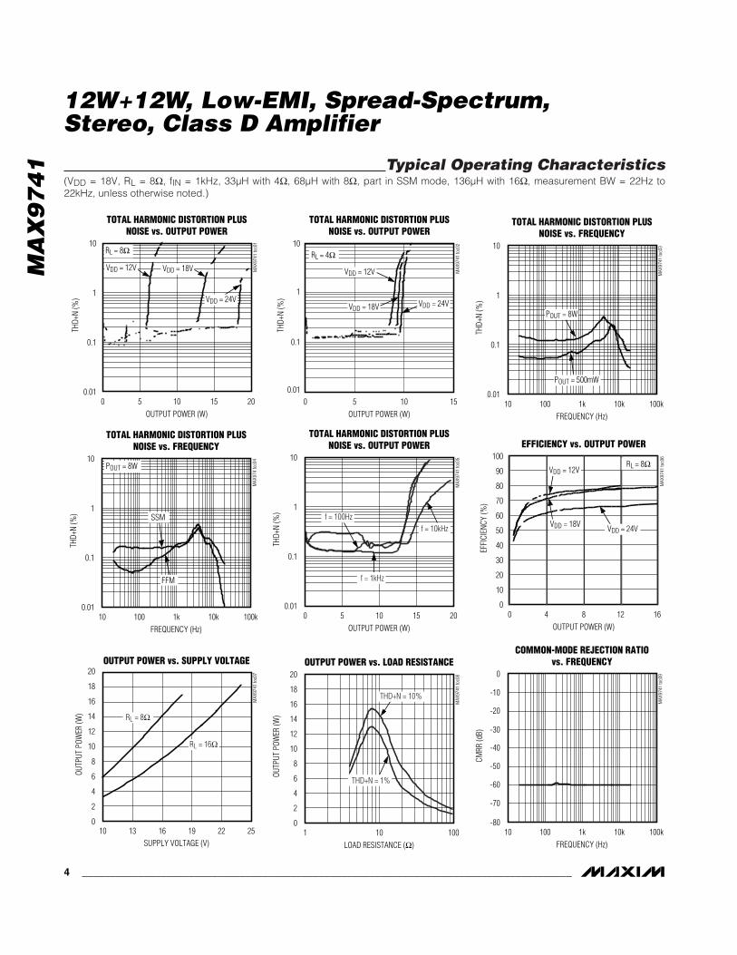
TOTAL HARMONIC DISTORTION PLUSNOISE vs. OUTPUT POWER
MAX
9741
toc0
1
OUTPUT POWER (W)
THD+
N (%
)
15105
0.1
1
10
0.010 20
RL = 8Ω
VDD = 24V
VDD = 18VVDD = 12V
15
TOTAL HARMONIC DISTORTION PLUSNOISE vs. OUTPUT POWER
MAX
9741
toc0
2
OUTPUT POWER (W)
THD+
N (%
)
0.01
0.1
1
10
0
RL = 4Ω
VDD = 24VVDD = 18V
VDD = 12V
105
TOTAL HARMONIC DISTORTION PLUSNOISE vs. FREQUENCY
MAX
9741
toc0
3
FREQUENCY (Hz)
THD+
N (%
)
10k1k100
0.1
1
10
0.0110 100k
POUT = 500mW
POUT = 8W
TOTAL HARMONIC DISTORTION PLUSNOISE vs. FREQUENCY
MAX
974
toc0
4
FREQUENCY (Hz)
THD+
N (%
)
10k1k100
0.1
1
10
0.0110 100k
POUT = 8W
SSM
FFM
OUTPUT POWER vs. SUPPLY VOLTAGE
MAX
9741
toc0
7
SUPPLY VOLTAGE (V)
OUTP
UT P
OWER
(W)
0
6
4
2
8
10
12
14
16
18
20
10 1613 19 22 25
RL = 8Ω
RL = 16Ω
TOTAL HARMONIC DISTORTION PLUSNOISE vs. OUTPUT POWER
MAX
9741
toc0
5
OUTPUT POWER (W)
THD+
N (%
)
15105
0.1
1
10
0.010 20
f = 100Hzf = 10kHz
f = 1kHz
EFFICIENCY vs. OUTPUT POWER
MAX
9741
toc0
6
OUTPUT POWER (W)
EFFI
CIEN
CY (%
)
16124 8
10
20
30
40
50
60
70
80
90
100
00
RL = 8Ω
VDD = 18V
VDD = 12V
VDD = 24V
OUTPUT POWER vs. LOAD RESISTANCE
MAX
9741
toc0
8
LOAD RESISTANCE (Ω)
OUTP
UT P
OWER
(W)
10
2
4
6
8
10
12
14
16
18
20
01 100
THD+N = 10%
THD+N = 1%
COMMON-MODE REJECTION RATIOvs. FREQUENCY
MAX
9741
toc0
9
FREQUENCY (Hz)
CMRR
(dB)
10k1k100
-70
-60
-50
-40
-30
-20
-10
0
-8010 100k
Typical Operating Characteristics(VDD = 18V, RL = 8Ω, fIN = 1kHz, 33µH with 4Ω, 68µH with 8Ω, part in SSM mode, 136µH with 16Ω, measurement BW = 22Hz to22kHz, unless otherwise noted.)
MA
X9
74
1
12W+12W, Low-EMI, Spread-Spectrum, Stereo, Class D Amplifier
_______________________________________________________________________________________ 5
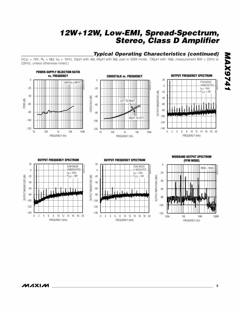
POWER-SUPPLY REJECTION RATIOvs. FREQUENCY
MAX
9741
toc1
0
FREQUENCY (Hz)
PSRR
(dB)
10k1k100
-100
-80
-60
-40
-20
0
-12010 100k
200mVP-P INPUT
CROSSTALK vs. FREQUENCY
MAX
9741
toc1
1
FREQUENCY (Hz)
CROS
STAL
K (d
B)
10k1k100
-80
-100
-60
-40
-20
0
-12010 100k
LEFT TO RIGHT
RIGHT TO LEFT
OUTPUT FREQUENCY SPECTRUM
MAX
9741
toc1
2
FREQUENCY (kHz)
OUTP
UT M
AGNI
TUDE
(dB)
-120
-100
-80
-60
-40
-20
0
20
-140181612 144 6 8 1020 20
FFM MODEUNWEIGHTEDfIN = 1kHzPOUT = 5W
OUTPUT FREQUENCY SPECTRUM
MAX
941
toc1
3
FREQUENCY (kHz)
OUTP
UT M
AGNI
TUDE
(dB)
-120
-100
-80
-60
-40
-20
0
20
-140181612 144 6 8 1020 20
SSM MODEUNWEIGHTEDfIN = 1kHzPOUT = 5W
OUTPUT FREQUENCY SPECTRUM
MAX
9741
toc1
4
FREQUENCY (kHz)
OUTP
UT M
AGNI
TUDE
(dB)
-120
-100
-80
-60
-40
-20
0
20
-140181612 144 6 8 1020 20
SSM MODEA-WEIGHTEDfIN = 1kHzPOUT = 5W
100k 1M 10M 100M
WIDEBAND OUTPUT SPECTRUM(FFM MODE)
MAX
9741
toc1
5
FREQUENCY (Hz)
OUTP
UT A
MPL
ITUD
E (d
BV)
0
-120
-100
-80
-60
-40
-20
RBW = 10kHz
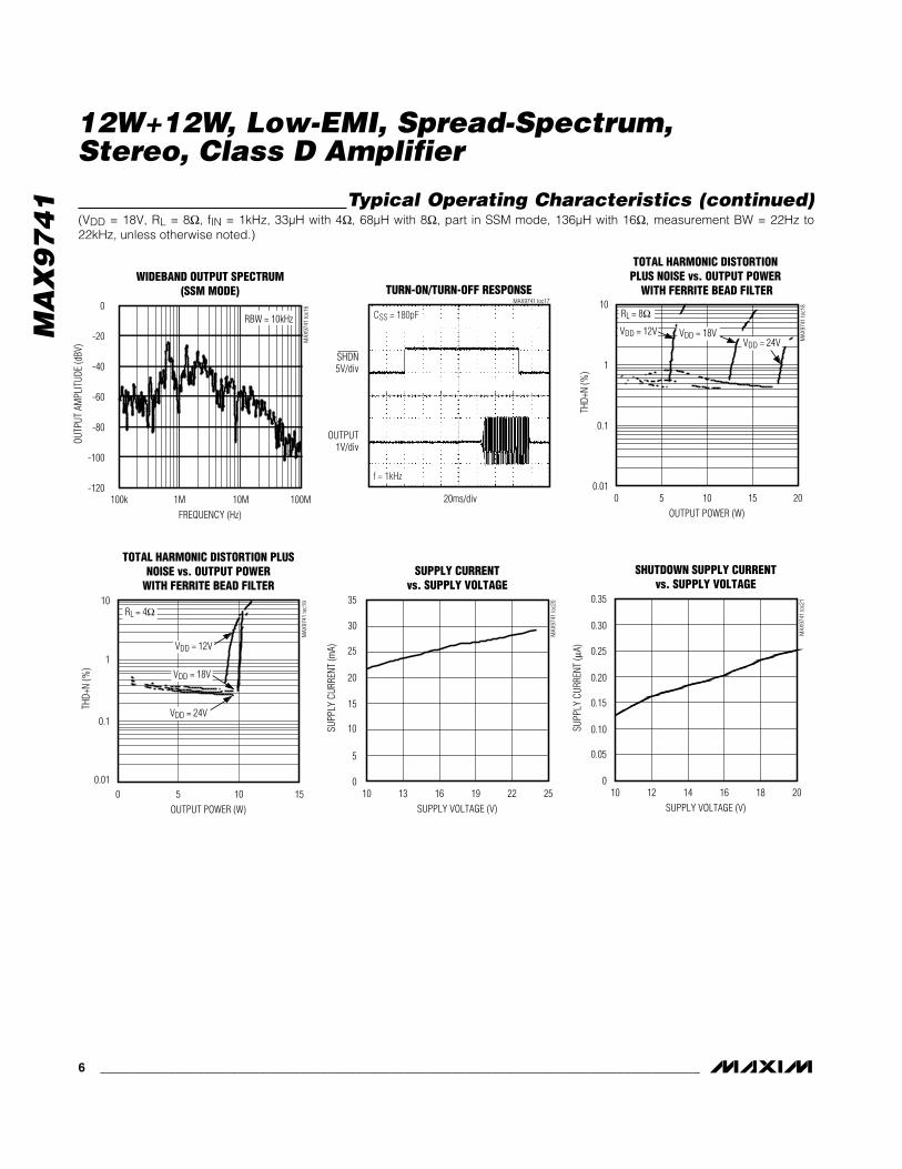
Typical Operating Characteristics (continued)(VDD = 18V, RL = 8Ω, fIN = 1kHz, 33µH with 4Ω, 68µH with 8Ω, part in SSM mode, 136µH with 16Ω, measurement BW = 22Hz to22kHz, unless otherwise noted.)
MA
X9
74
1
12W+12W, Low-EMI, Spread-Spectrum, Stereo, Class D Amplifier
6 _______________________________________________________________________________________
15
TOTAL HARMONIC DISTORTION PLUSNOISE vs. OUTPUT POWER
WITH FERRITE BEAD FILTER
MAX
9741
toc1
9
OUTPUT POWER (W)
THD+
N (%
)
0.01
0.1
1
10
0
RL = 4Ω
105
VDD = 18V
VDD = 12V
VDD = 24V
SUPPLY CURRENTvs. SUPPLY VOLTAGE
MAX
9741
toc2
0
SUPPLY VOLTAGE (V)
SUPP
LY C
URRE
NT (m
A)
22191613
10
5
15
20
25
30
35
010 25
SHUTDOWN SUPPLY CURRENTvs. SUPPLY VOLTAGE
MAX
9741
toc2
1SUPPLY VOLTAGE (V)
SUPP
LY C
URRE
NT (µ
A)
18161412
0.10
0.05
0.15
0.20
0.25
0.30
0.35
010 20
Typical Operating Characteristics (continued)(VDD = 18V, RL = 8Ω, fIN = 1kHz, 33µH with 4Ω, 68µH with 8Ω, part in SSM mode, 136µH with 16Ω, measurement BW = 22Hz to22kHz, unless otherwise noted.)
100k 1M 10M 100M
WIDEBAND OUTPUT SPECTRUM(SSM MODE)
MAX
9741
toc1
6
FREQUENCY (Hz)
OUTP
UT A
MPL
ITUD
E (d
BV)
0
-120
-100
-80
-60
-40
-20
RBW = 10kHz
TURN-ON/TURN-OFF RESPONSEMAX9741 toc17
20ms/div
OUTPUT1V/div
SHDN5V/div
f = 1kHz
CSS = 180pF
TOTAL HARMONIC DISTORTION PLUS NOISE vs. OUTPUT POWER
WITH FERRITE BEAD FILTER
MAX
9741
toc1
8
OUTPUT POWER (W)
THD+
N (%
)
15105
0.1
1
10
0.010 20
RL = 8Ω
VDD = 18VVDD = 12VVDD = 24V
MA
X9
74
1
12W+12W, Low-EMI, Spread-Spectrum, Stereo, Class D Amplifier
_______________________________________________________________________________________ 7
Detailed DescriptionThe MAX9741 low-EMI, Class D audio power amplifierfeatures several improvements to switch-mode amplifi-er technology. This device offers Class AB perfor-mance with Class D efficiency, while occupyingminimal board space. A unique modulation scheme
and spread-spectrum switching mode create a com-pact, flexible, low-noise, efficient audio power amplifier.The differential input architecture reduces common-mode noise pickup, and can be used without input-coupling capacitors. The device can also beconfigured as a single-ended input amplifier.
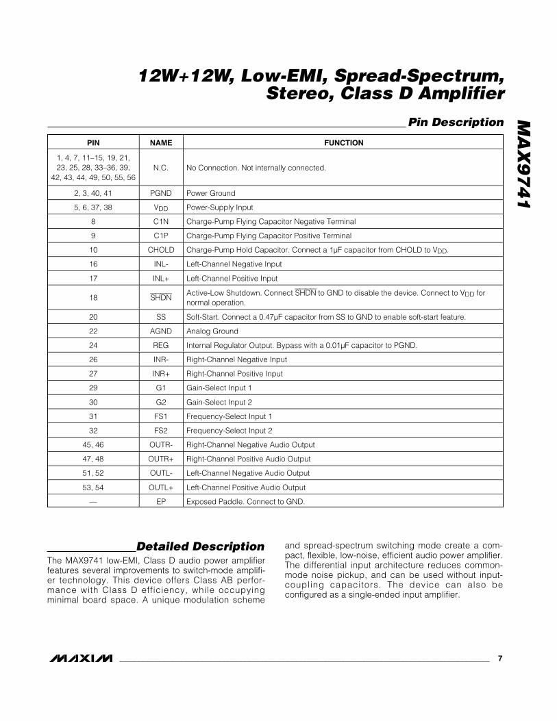
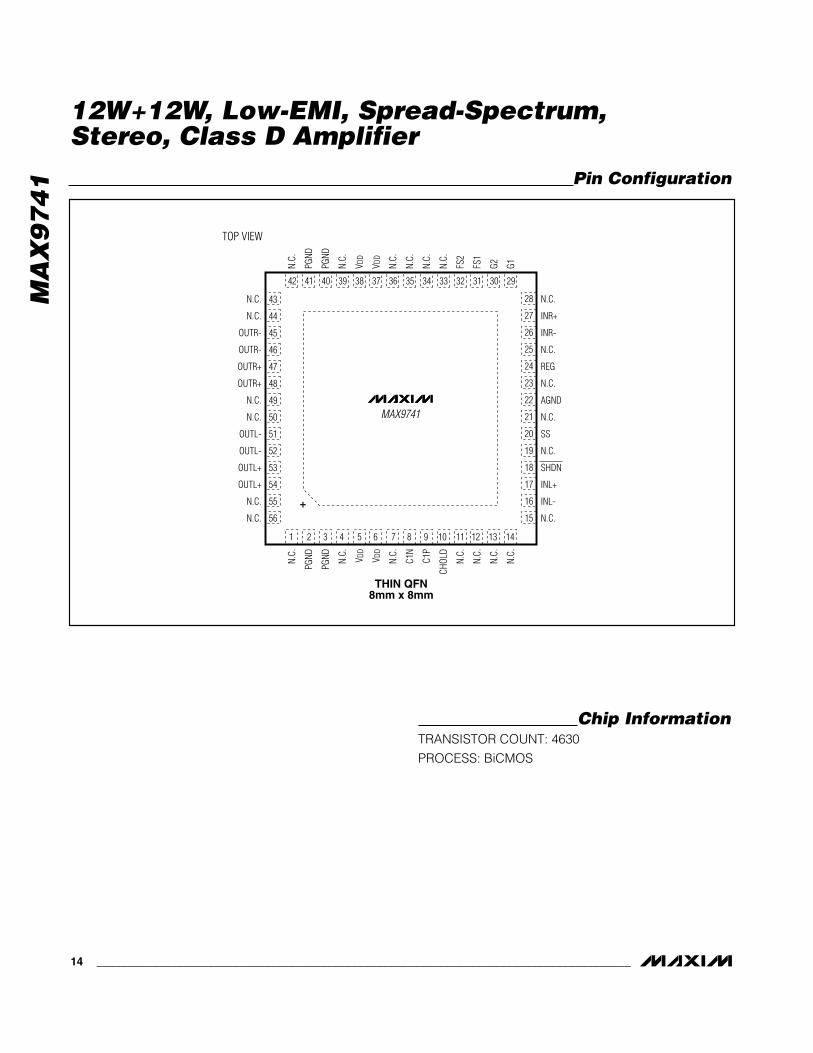
PIN NAME FUNCTION
1, 4, 7, 11–15, 19, 21,23, 25, 28, 33–36, 39,
42, 43, 44, 49, 50, 55, 56N.C. No Connection. Not internally connected.
2, 3, 40, 41 PGND Power Ground
5, 6, 37, 38 VDD Power-Supply Input
8 C1N Charge-Pump Flying Capacitor Negative Terminal
9 C1P Charge-Pump Flying Capacitor Positive Terminal
10 CHOLD Charge-Pump Hold Capacitor. Connect a 1µF capacitor from CHOLD to VDD.
16 INL- Left-Channel Negative Input
17 INL+ Left-Channel Positive Input
18 SHDNActive-Low Shutdown. Connect SHDN to GND to disable the device. Connect to VDD fornormal operation.
20 SS Soft-Start. Connect a 0.47µF capacitor from SS to GND to enable soft-start feature.
22 AGND Analog Ground
24 REG Internal Regulator Output. Bypass with a 0.01µF capacitor to PGND.
26 INR- Right-Channel Negative Input
27 INR+ Right-Channel Positive Input
29 G1 Gain-Select Input 1
30 G2 Gain-Select Input 2
31 FS1 Frequency-Select Input 1
32 FS2 Frequency-Select Input 2
45, 46 OUTR- Right-Channel Negative Audio Output
47, 48 OUTR+ Right-Channel Positive Audio Output
51, 52 OUTL- Left-Channel Negative Audio Output
53, 54 OUTL+ Left-Channel Positive Audio Output
— EP Exposed Paddle. Connect to GND.
Pin Description
Operating ModesFixed-Frequency Modulation (FFM) Mode
The MAX9741 features three FFM modes with differentswitching frequencies (Table 1). In FFM mode, the fre-quency spectrum of the Class D output consists of thefundamental switching frequency and its associatedharmonics (see the Wideband Output Spectrum graphin the Typical Operating Characteristics). The MAX9741allows the switching frequency to be changed by±35%, should the frequency of one or more of the har-monics fall in a sensitive band. This can be done at anytime and does not affect audio reproduction.
Spread-Spectrum Modulation (SSM) ModeA unique, proprietary spread-spectrum mode flattensthe wideband spectral components, improving EMIemissions that may be radiated by the speaker andcables. This mode is enabled by setting FS1 = FS2 =H. In SSM mode, the switching frequency varies ran-domly by ±7% around the center frequency (670kHz).The modulation scheme remains the same, but theperiod of the triangle waveform changes from cycle tocycle. Instead of a large amount of spectral energy pre-sent at multiples of the switching frequency, the energyis now spread over a bandwidth that increases with fre-quency. Above a few megahertz, the wideband spec-trum looks like white noise for EMI purposes.
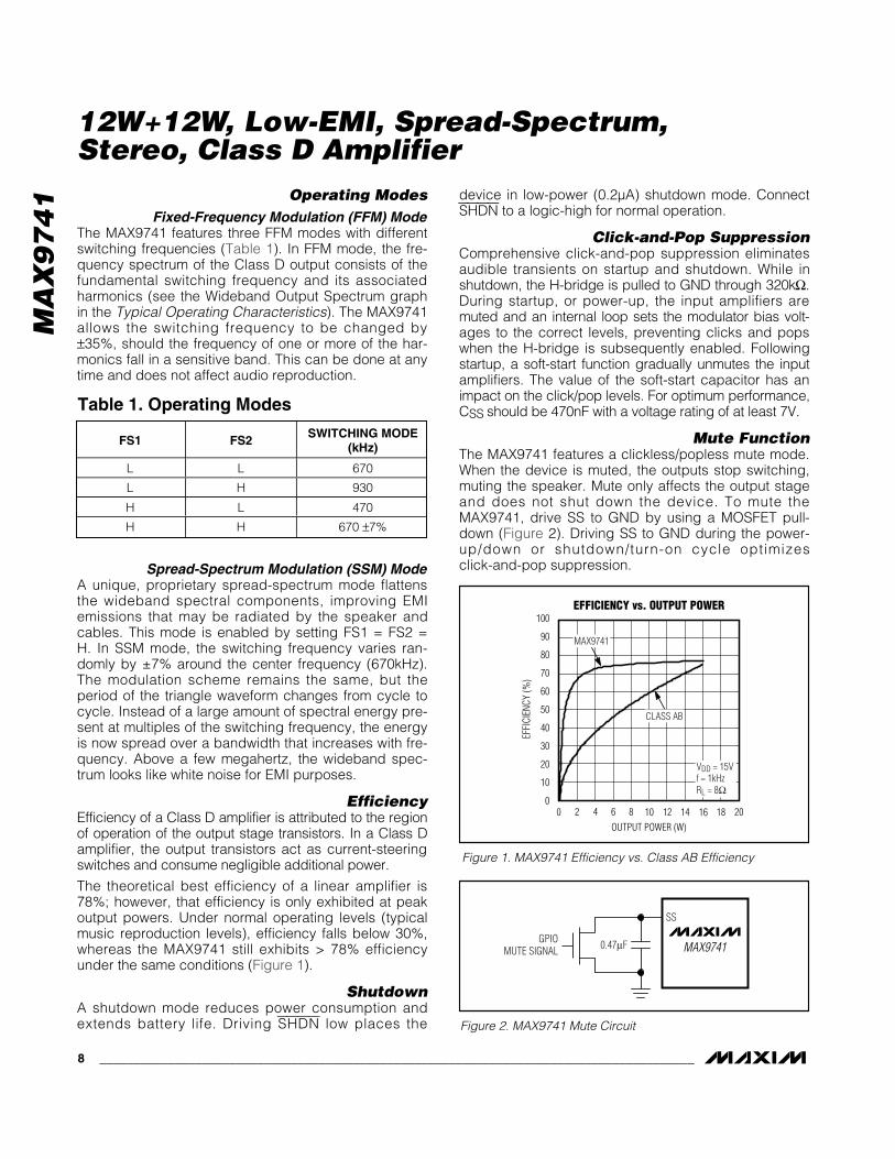
EfficiencyEfficiency of a Class D amplifier is attributed to the regionof operation of the output stage transistors. In a Class Damplifier, the output transistors act as current-steeringswitches and consume negligible additional power.
The theoretical best efficiency of a linear amplifier is78%; however, that efficiency is only exhibited at peakoutput powers. Under normal operating levels (typicalmusic reproduction levels), efficiency falls below 30%,whereas the MAX9741 still exhibits > 78% efficiencyunder the same conditions (Figure 1).
ShutdownA shutdown mode reduces power consumption andextends battery life. Driving SHDN low places the
device in low-power (0.2µA) shutdown mode. ConnectSHDN to a logic-high for normal operation.
Click-and-Pop SuppressionComprehensive click-and-pop suppression eliminatesaudible transients on startup and shutdown. While inshutdown, the H-bridge is pulled to GND through 320kΩ.During startup, or power-up, the input amplifiers aremuted and an internal loop sets the modulator bias volt-ages to the correct levels, preventing clicks and popswhen the H-bridge is subsequently enabled. Followingstartup, a soft-start function gradually unmutes the inputamplifiers. The value of the soft-start capacitor has animpact on the click/pop levels. For optimum performance,CSS should be 470nF with a voltage rating of at least 7V.
Mute FunctionThe MAX9741 features a clickless/popless mute mode.When the device is muted, the outputs stop switching,muting the speaker. Mute only affects the output stageand does not shut down the device. To mute theMAX9741, drive SS to GND by using a MOSFET pull-down (Figure 2). Driving SS to GND during the power-up/down or shutdown/turn-on cycle optimizesclick-and-pop suppression.
MA
X9
74
1
12W+12W, Low-EMI, Spread-Spectrum, Stereo, Class D Amplifier
8 _______________________________________________________________________________________
MAX9741
SS
0.47µFGPIOMUTE SIGNAL
Figure 2. MAX9741 Mute Circuit
Table 1. Operating Modes
FS1 FS2 SWITCHING MODE(kHz)
L L 670
L H 930
H L 470
H H 670 ±7%
Figure 1. MAX9741 Efficiency vs. Class AB Efficiency
0
30
20
10
40
50
60
70
80
90
100
0 6 8 10 12 14 16 182 4 20
EFFICIENCY vs. OUTPUT POWER
OUTPUT POWER (W)
EFFI
CIEN
CY (%
)
VDD = 15Vf = 1kHzRL = 8Ω
MAX9741
CLASS AB
MA
X9
74
1
12W+12W, Low-EMI, Spread-Spectrum, Stereo, Class D Amplifier
_______________________________________________________________________________________ 9
Internal RegulatorThe MAX9741 has an internal linear regulator, REG,used to power the internal analog circuitry. The voltageat REG is nominally 6V. Bypass REG to AGND with a10nF capacitor, rated for at least 10V. REG is turned offin shutdown.
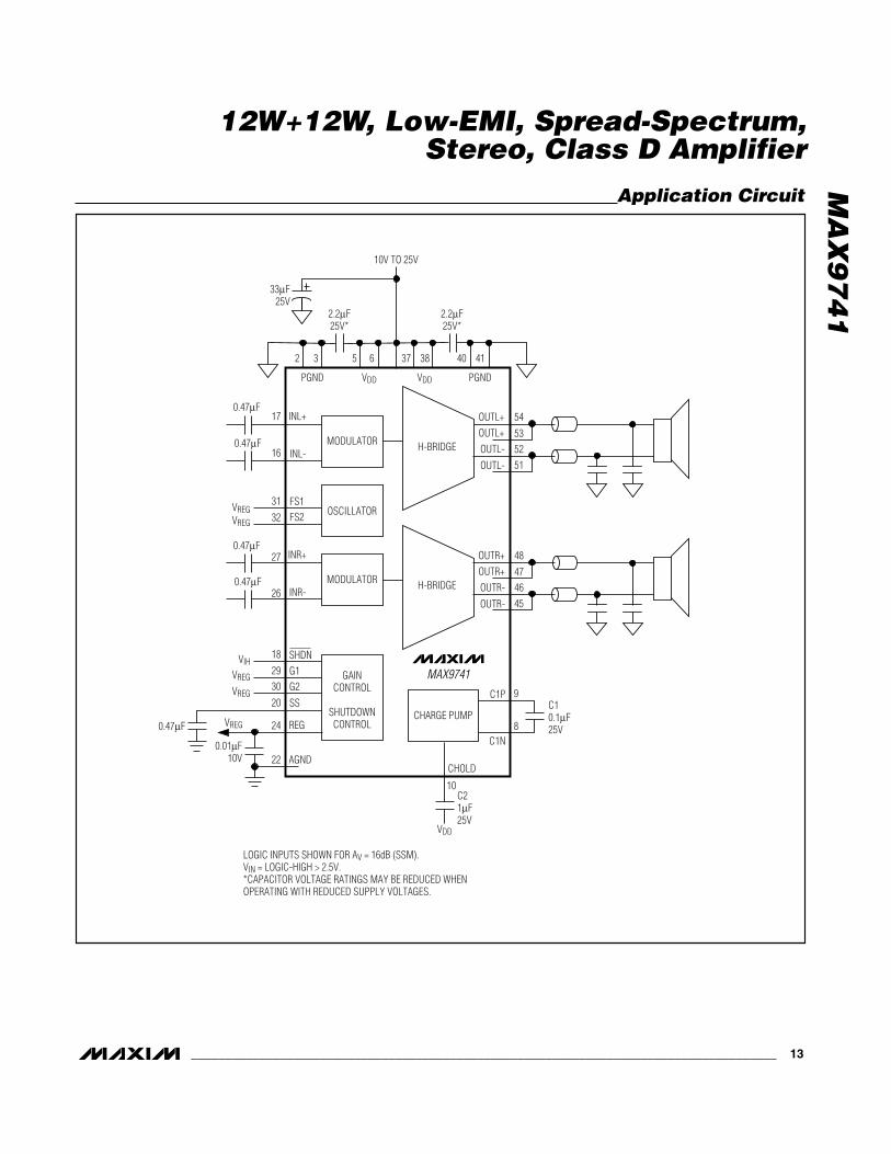
Applications InformationClass D Amplifier Outputs
Class D amplifiers differ from analog amplifiers such asClass AB in that their output waveform is composed ofhigh-frequency pulses from ground to the supply rail.When viewed with an oscilloscope the audio signal willnot be seen; instead, the high-frequency pulses domi-nate. To evaluate the output of a Class D amplifierrequires taking the difference from the positive andnegative outputs, then lowpass filtering the differenceto recover the amplified audio signal.
Ferrite Bead Output FiltersThe MAX9741’s low-EMI output switching methodreduces the output filtering requirements when compared
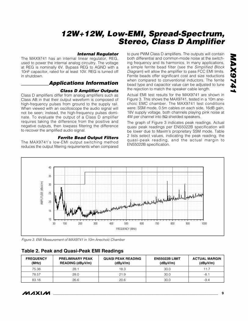
to pure PWM Class D amplifiers. The outputs will containboth differential and common-mode noise at the switch-ing frequency and its harmonics. In many applications,a simple ferrite bead filter (see the Simplified BlockDiagram) will allow the amplifier to pass FCC EMI limits.Ferrite beads offer significant cost and size reductionswhen compared to conventional inductors. The ferritebead type and capacitor value can be adjusted to tunethe rejection to match the speaker cable length.
Actual EMI test results for the MAX9741 are shown inFigure 3. This shows the MAX9741, tested in a 10m ane-choic EMC chamber. The MAX9741 test conditionswere: SSM mode, 0.5m cables on each side, 16dB gain,18V supply voltage, both channels playing pink noise at4W per channel into 8Ω shielded speakers.
The graph of Figure 3 indicates peak readings. Actualquasi peak readings per EN55022B specification willbe lower due to Maxim’s proprietary SSM mode. Table2 lists select values, indicating the peak reading, thequasi-peak reading, and the actual margin toEN55022B specification.
FREQUENCY (MHz)
AMPL
ITUD
E (d
BuV/
m)
900800100 200 300 500 600400 70010
15
20
25
30
35
40
30 1000
Figure 3. EMI Measurement of MAX9741 in 10m Anechoic Chamber
Table 2. Peak and Quasi-Peak EMI Readings
FREQUENCY(MHz)
PRELIMINARY PEAKREADING (dBµV/m)
QUASI PEAK READING(dBµV/m)
EN55022B LIMIT(dBµV/m)
ACTUAL MARGIN(dBµV/m)
75.38 28.1 18.3 30.0 11.7
78.57 28.0 21.9 30.0 -8.1
83.18 26.6 20.6 30.0 -9.4
MA
X9
74
1
12W+12W, Low-EMI, Spread-Spectrum, Stereo, Class D Amplifier
10 ______________________________________________________________________________________
Ferrite beads are available from many manufacturers.Table 3 lists some manufacturers who make ferritebeads and other products suitable for use with Class Damplifiers.
Although they offer a low cost and small size, ferritebead filters slightly increase distortion and slightlyreduce efficiency. If the audio performance of the ferritebead filters does not meet the system requirements, thena full inductor/capacitor (LC) filter should be considered.
Inductor/Capacitor Output FiltersUsing a full inductor and capacitor (LC) output filterprovides significant attenuation of the fundamentalswitching energy.
Select inductors rated for the expected RMS currentload. For example, if using a Class D amplifier up to10W into 8Ω, the inductor should be rated for 1.25ARMS or more. Furthermore, the inductor should maintaina constant inductance value across the expected cur-rent range. Inductors which change in value as a func-tion of current will cause harmonic distortion.
The output capacitors can also affect audio perfor-mance. Ceramic capacitors are often selected for theirsize and cost advantage, but they cause distortion. Ifthe application constraints dictate ceramic capacitors,selecting higher voltage rating and larger package sizemitigates some of the shortcomings. Best performanceis obtained with plastic film capacitors, but these arelarger and more expensive.
Filterless OperationIn some cases, a Class D amplifier can be used withoutan output filter. The intrinsic inductance of the loud-speaker stores energy from the high-speed PWM pulses,
converting these into power in the audible frequencyrange. Filterless operation requires the Class D amplifi-er to be very close to the speaker. Distances greaterthan a few centimeters must be evaluated for EMCcompliance.
Gain SelectionTable 4 shows the suggested gain settings to attain amaximum output power from a given peak input voltageand given load.
Output OffsetUnlike a Class AB amplifier, the output offset voltage ofClass D amplifiers does not noticeably increase quies-cent current draw when a load is applied. This is due tothe power conversion of the Class D amplifier. Forexample, an 8mVDC offset across an 8Ω load results in1mA extra current consumption in a Class AB device.In the Class D case, an 8mV offset into 8Ω equates to an additional power drain of 8µW. Due to the high efficiency of the Class D amplifier, this represents anadditional quiescent current draw of: 8µW / (VDD / 100 η), which is in the order of a few microamps.
Input AmplifierDifferential Input
The MAX9741 features a differential input structure, mak-ing them compatible with many CODECs, and offeringimproved noise immunity over a single-ended input ampli-fier. In devices such as PCs, noisy digital signals can bepicked up by the amplifier’s input traces. The signalsappear at the amplifiers’ inputs as common-mode noise. Adifferential input amplifier amplifies the difference of thetwo inputs, any signal common to both inputs is canceled.
Table 4. Gain SettingsG1 G2 GAIN (dB)
0 0 29.6
0 1 19.1
1 0 13
1 1 16
Table 3. Filter Component SuppliersSUPPLIER PRODUCT WEBSITE
MurataFerrite beads,capacitors
www.murata.com
Taiyo YudenFerrite beads,capacitors
www.t-yuden.com
TDKFerrite beads,capacitors
www.tdk.co.jp/tetop01
Fairrite Ferrite beads www.fair-rite.com
Coilcraft Inductors www.coilcraft.com
Sumida Inductors www.sumida.com
Panasonic Inductorswww.panasonic.com/industrial/components
MA
X9
74
1
12W+12W, Low-EMI, Spread-Spectrum, Stereo, Class D Amplifier
______________________________________________________________________________________ 11
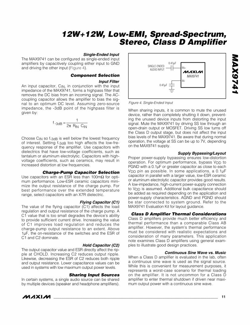
Single-Ended InputThe MAX9741 can be configured as single-ended inputamplifiers by capacitively coupling either input to GNDand driving the other input (Figure 4).
Component SelectionInput Filter
An input capacitor, CIN, in conjunction with the inputimpedance of the MAX9741, forms a highpass filter thatremoves the DC bias from an incoming signal. The AC-coupling capacitor allows the amplifier to bias the sig-nal to an optimum DC level. Assuming zero-sourceimpedance, the -3dB point of the highpass filter isgiven by:
Choose CIN so f-3dB is well below the lowest frequencyof interest. Setting f-3dB too high affects the low-fre-quency response of the amplifier. Use capacitors withdielectrics that have low-voltage coefficients, such astantalum or aluminum electrolytic. Capacitors with high-voltage coefficients, such as ceramics, may result inincreased distortion at low frequencies.
Charge-Pump Capacitor SelectionUse capacitors with an ESR less than 100mΩ for opti-mum performance. Low-ESR ceramic capacitors mini-mize the output resistance of the charge pump. Forbest performance over the extended temperaturerange, select capacitors with an X7R dielectric.
Flying Capacitor (C1)The value of the flying capacitor (C1) affects the loadregulation and output resistance of the charge pump. AC1 value that is too small degrades the device’s abilityto provide sufficient current drive. Increasing the valueof C1 improves load regulation and reduces thecharge-pump output resistance to an extent. Above1µF, the on-resistance of the switches and the ESR ofC1 and C2 dominate.
Hold Capacitor (C2)The output capacitor value and ESR directly affect the rip-ple at CHOLD. Increasing C2 reduces output ripple.Likewise, decreasing the ESR of C2 reduces both rippleand output resistance. Lower capacitance values can beused in systems with low maximum output power levels.
Sharing Input SourcesIn certain systems, a single audio source can be sharedby multiple devices (speaker and headphone amplifiers).
When sharing inputs, it is common to mute the unuseddevice, rather than completely shutting it down, prevent-ing the unused device inputs from distorting the inputsignal. Mute the MAX9741 by driving SS low through anopen-drain output or MOSFET. Driving SS low turns offthe Class D output stage, but does not affect the inputbias levels of the MAX9741. Be aware that during normaloperation, the voltage at SS can be up to 7V, dependingon the MAX9741 supply.
Supply Bypassing/LayoutProper power-supply bypassing ensures low-distortionoperation. For optimum performance, bypass VDD toPGND with a 0.1µF or greater capacitor as close to eachVDD pin as possible. In some applications, a 0.1µFcapacitor in parallel with a larger value, low-ESR ceramicor aluminum electrolytic capacitor provides good results.A low-impedance, high-current power-supply connectionto VDD is assumed. Additional bulk capacitance shouldbe added as required depending on the application andpower-supply characteristics. AGND and PGND shouldbe star connected to system ground. Refer to theMAX9741 Evaluation Kit for layout guidance.
Class D Amplifier Thermal ConsiderationsClass D amplifiers provide much better efficiency andthermal performance than a comparable Class ABamplifier. However, the system’s thermal performancemust be considered with realistic expectations andconsideration of many parameters. This applicationnote examines Class D amplifiers using general exam-ples to illustrate good design practices.
Continuous Sine Wave vs. MusicWhen a Class D amplifier is evaluated in the lab, oftena continuous sine wave is used as the signal source.While this is convenient for measurement purposes, itrepresents a worst-case scenario for thermal loadingon the amplifier. It is not uncommon for a Class Damplifier to enter thermal shutdown if driven near maxi-mum output power with a continuous sine wave.
fR C -3dB
IN IN
12
=π
MAX9741
IN+
IN-
0.47µF
0.47µF
SINGLE-ENDEDAUDIO INPUT
Figure 4. Single-Ended Input
MA
X9
74
1
12W+12W, Low-EMI, Spread-Spectrum, Stereo, Class D Amplifier
12 ______________________________________________________________________________________
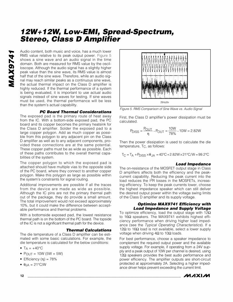
Audio content, both music and voice, has a much lowerRMS value relative to its peak output power. Figure 5shows a sine wave and an audio signal in the timedomain. Both are measured for RMS value by the oscil-loscope. Although the audio signal has a slightly higherpeak value than the sine wave, its RMS value is almosthalf that of the sine wave. Therefore, while an audio sig-nal may reach similar peaks as a continuous sine wave,the actual thermal impact on the Class D amplifier ishighly reduced. If the thermal performance of a systemis being evaluated, it is important to use actual audiosignals instead of sine waves for testing. If sine wavesmust be used, the thermal performance will be lessthan the system’s actual capability.
PC Board Thermal ConsiderationsThe exposed pad is the primary route of heat awayfrom the IC. With a bottom-side exposed pad, the PCboard and its copper becomes the primary heatsink forthe Class D amplifier. Solder the exposed pad to alarge copper polygon. Add as much copper as possi-ble from this polygon to any adjacent pin on the ClassD amplifier as well as to any adjacent components, pro-vided these connections are at the same potential.These copper paths must be as wide as possible. Eachof these paths contributes to the overall thermal capa-bilities of the system.
The copper polygon to which the exposed pad isattached should have multiple vias to the opposite sideof the PC board, where they connect to another copperpolygon. Make this polygon as large as possible withinthe system’s constraints for signal routing.
Additional improvements are possible if all the tracesfrom the device are made as wide as possible.Although the IC pins are not the primary thermal pathout of the package, they do provide a small amount.The total improvement would not exceed approximately10%, but it could make the difference between accept-able performance and thermal problems.
With a bottomside exposed pad, the lowest resistancethermal path is on the bottom of the PC board. The topsideof the IC is not a significant thermal path for the device.
Thermal CalculationsThe die temperature of a Class D amplifier can be esti-mated with some basic calculations. For example, thedie temperature is calculated for the below conditions:
• TA = +40°C
• POUT = 10W (5W + 5W)
• Efficiency (η) = 78%
• θJA = 21°C/W
First, the Class D amplifier’s power dissipation must becalculated.
Then the power dissipation is used to calculate the dietemperature, TC, as follows:
Load ImpedanceThe on-resistance of the MOSFET output stage in ClassD amplifiers affects both the efficiency and the peak-current capability. Reducing the peak current into theload reduces the I2R losses in the MOSFETs, increas-ing efficiency. To keep the peak currents lower, choosethe highest impedance speaker which can still deliverthe desired output power within the voltage swing limitsof the Class D amplifier and its supply voltage.
Optimize MAX9741 Efficiency withLoad Impedance and Supply Voltage
To optimize efficiency, load the output stage with 12Ωto 16Ω speakers. The MAX9741 exhibits highest effi-ciency performance when driving higher load imped-ance (see the Typical Operating Characteristics). If a12Ω to 16Ω load is not available, select a lower supplyvoltage when driving 4Ω to 10Ω loads.
For best performance, choose a speaker impedance tocomplement the required output power and the availablesupply voltage. For example, if operating from a 24V sup-ply and a peak output of 10W per channel is desired, using12Ω speakers provides the best audio performance andpower efficiency. The amplifier outputs are short-circuitprotected at approximately 2A. Selecting a higher imped-ance driver helps prevent exceeding the current limit.
T T P C W C W CC A DISS JA= + × = ° + × ° = °θ 40 2 82 21 99 2. / .
PP
PW
W WDISSOUT
OUT= = =− −η
1078
10 2 82%
.
20ms/div
Figure 5. RMS Comparison of Sine Wave vs. Audio Signal
MA
X9
74
1
12W+12W, Low-EMI, Spread-Spectrum, Stereo, Class D Amplifier
______________________________________________________________________________________ 13
MAX9741
0.47µF
LOGIC INPUTS SHOWN FOR AV = 16dB (SSM).VIN = LOGIC-HIGH > 2.5V.*CAPACITOR VOLTAGE RATINGS MAY BE REDUCED WHENOPERATING WITH REDUCED SUPPLY VOLTAGES.
INL+17
16
31
18
2930
20
22 AGND
24
9
8
32
INL-
FS1VREGVREG
VREG
VREG
FS2
G1G2
SS
REG
0.47µF MODULATOR
OSCILLATOR
CHARGE PUMP
C1PC10.1µF25V
C1N0.47µF
VIH
GAINCONTROL
SHUTDOWNCONTROL
0.01µF10V
SHDN
H-BRIDGE
OUTL+OUTL+OUTL-
OUTL-
54
535251
PGND VDD VDD PGND
2 5 6 37 38 40 413
10V TO 25V
33µF25V
2.2µF25V*
2.2µF25V*
C21µF25V
CHOLD
VDD
10
0.47µFINR+
26
27
INR-0.47µF MODULATOR H-BRIDGE
OUTR+OUTR+OUTR-
OUTR-
48
474645
VREG
Application Circuit
MA
X9
74
1
12W+12W, Low-EMI, Spread-Spectrum, Stereo, Class D Amplifier
14 ______________________________________________________________________________________
TOP VIEW
MAX9741
THIN QFN8mm x 8mm
15
17
16
18
19
20
21
22
23
24
25
26
27
28
N.C.
INL-
INL+
SHDN
N.C.
SS
N.C.
AGND
N.C.
REG
N.C.
INR-
INR+
N.C.
N.C.
N.C.
OUTL+
OUTL+
OUTL-
OUTL-
N.C.
N.C.
OUTR+
OUTR+
OUTR-
OUTR-
N.C.
N.C.
48
47
46
45
44
43
54
53
56
55
52
51
50
49
1 2 3 4 5 6 7 8 9 10 11 12 13 14
42 41 40 39 38 37 36 35 34 33 32 31 30 29
N.C.
N.C.
N.C.
N.C.
CHOL
D
C1P
C1N
N.C.
V DD
V DD
N.C.
PGND
PGNDN.C.
FS1
G2 G1FS2
N.C.
N.C.
N.C.
N.C.
V DD
V DD
N.C.
PGND
PGND
N.C.
+
Pin Configuration
Chip InformationTRANSISTOR COUNT: 4630
PROCESS: BiCMOS
MA
X9
74
1
12W+12W, Low-EMI, Spread-Spectrum, Stereo, Class D Amplifier
______________________________________________________________________________________ 15
56L
THIN
QFN
.EP
S
PACKAGE OUTLINE
21-0135 21
E
56L THIN QFN, 8x8x0.8mm
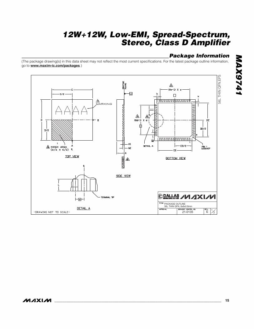
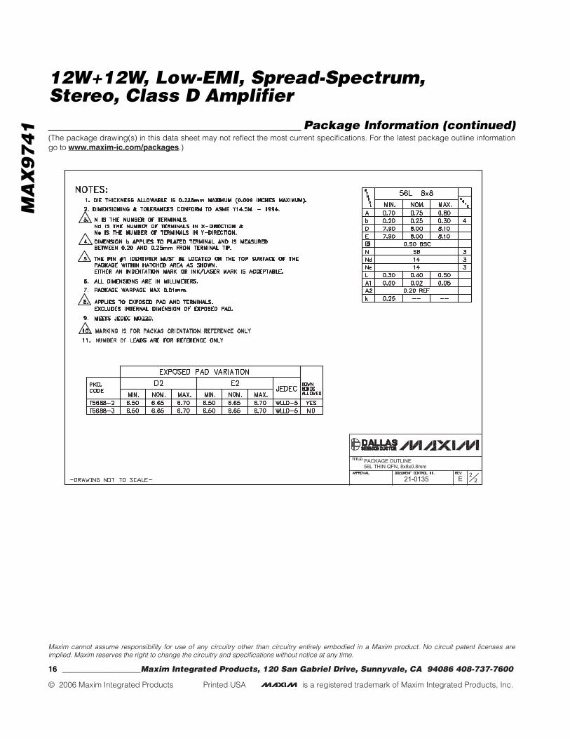
Package Information(The package drawing(s) in this data sheet may not reflect the most current specifications. For the latest package outline information,go to www.maxim-ic.com/packages.)
MA
X9
74
1
12W+12W, Low-EMI, Spread-Spectrum, Stereo, Class D Amplifier
Maxim cannot assume responsibility for use of any circuitry other than circuitry entirely embodied in a Maxim product. No circuit patent licenses areimplied. Maxim reserves the right to change the circuitry and specifications without notice at any time.
16 ____________________Maxim Integrated Products, 120 San Gabriel Drive, Sunnyvale, CA 94086 408-737-7600
© 2006 Maxim Integrated Products Printed USA is a registered trademark of Maxim Integrated Products, Inc.
Quijano
PACKAGE OUTLINE
21-0135 22
E
56L THIN QFN, 8x8x0.8mm
Package Information (continued)(The package drawing(s) in this data sheet may not reflect the most current specifications. For the latest package outline informationgo to www.maxim-ic.com/packages.)
Related Documents