1 2004 MAPLD VHDL Design Review VHDL Design Review And Presentation

Welcome message from author
This document is posted to help you gain knowledge. Please leave a comment to let me know what you think about it! Share it to your friends and learn new things together.
Transcript

12004 MAPLD VHDL Design Review
VHDL Design ReviewAnd
Presentation

22004 MAPLD VHDL Design Review
Designer’s Responsibilities(Besides Doing the Design):
• Make the design reviewable and transferable– Documentation
• Theory of operation• Proof that spec and WCA are met
– Organization• Partitioning into logical components
– Presentation• Readability of schematics, VHDL, etc.
• Inadequate documentation biggest design review problem– How would you, the designer, explain your design to someone
else?• Reviewer’s question: If the designer can’t present the
design, does the designer understand the design?

32004 MAPLD VHDL Design Review
How to Review VHDL Designs
• How does one perform a design review, in general?– Most design review tasks are independent of how the
design is presented
• What does VHDL add to the task?

42004 MAPLD VHDL Design Review
What VHDL Adds to the Review Process
• Probably, an awful lot more work!!• VHDL introduces serious problems:
– It hides design details– It is not WYSIWYG: What you see (as your design
concept in VHDL) may not be what you get (as an output of the synthesizer)
– Coupled with FPGAs, it encourages bad design practices
• Understanding design by reading code extremely difficult

52004 MAPLD VHDL Design Review
VHDL Hides Design Details
• Connectivity hard to follow in VHDL files
• Behavior of sequential circuits can be hard to follow through processes
• Interactions between modules can be difficult to understand
• Spelling errors → undetected circuit errors

62004 MAPLD VHDL Design Review
Following connectivity
• Signal name changes make task difficult• My method as a reviewer:
– Import modules into Libero– Create symbols for modules– Create a schematic with modules and print it
out on E-size paper– Connect modules with colored pencils
• Designer should do this as part of design presentation

72004 MAPLD VHDL Design Review
Following ConnectivitySimple Input and Output Example
MA1: COUNT23 port map (RST_N => SIM_CLR_N, SYNC_CLR => EQUALS_internal, CLOCK => C5MHZ, Q => TIME_NOW_internal ); MA3: MUX_23_4 port map (A => R1HZ, B => R6HZ, C => R8HZ, D => R10HZ, T => THZ, T_SEL => TEST_SEQ, S1 => RATE_SEL(1), S0 => RATE_SEL(0), Y => Y ); MA2: COMP23 port map (DATAA => TIME_NOW_internal, DATAB=> Y, AEB => EQUALS_internal ); MA7: GATE_RANGE port map (RST_N => RST_N, CLOCK => C5MHZ, OPEN_VALUE => OPEN_VALUE,CLOSE_VALUE => CLOSE_VALUE, TIME_NOW => TIME_NOW_internal, GATE => GATE ); MA8: BIN2GRAY23 port map (A => TIME_NOW_internal, Y => GRAYTIME );
EQUALS <= EQUALS_internal; TIME_NOW <= TIME_NOW_internal;end RTL_ARCH;
Note: Had to print out the entity just to make this slide.
InputsOutputs

82004 MAPLD VHDL Design Review
Following ConnectivitySignals In a Simple Module
MA1: COUNT23 port map (RST_N => SIM_CLR_N, SYNC_CLR => EQUALS_internal, CLOCK => C5MHZ, Q => TIME_NOW_internal ); MA3: MUX_23_4 port map (A => R1HZ, B => R6HZ, C => R8HZ, D => R10HZ, T => THZ, T_SEL => TEST_SEQ, S1 => RATE_SEL(1), S0 => RATE_SEL(0), Y => Y ); MA2: COMP23 port map (DATAA => TIME_NOW_internal, DATAB=> Y, AEB => EQUALS_internal ); MA7: GATE_RANGE port map (RST_N => RST_N, CLOCK => C5MHZ, OPEN_VALUE => OPEN_VALUE,CLOSE_VALUE => CLOSE_VALUE, TIME_NOW => TIME_NOW_internal, GATE => GATE ); MA8: BIN2GRAY23 port map (A => TIME_NOW_internal, Y => GRAYTIME );
EQUALS <= EQUALS_internal; TIME_NOW <= TIME_NOW_internal;end RTL_ARCH;
Making this chart was a lot of work and was error prone.

92004 MAPLD VHDL Design Review
E.g., A Spelling Error?
• A VHDL module contained two signals:– CSEN appeared only on the left side of a
replacement statement:CSEN <= …
– CS_EN sourced several signals, i.e., appeared on the right side
X <= CS_EN…
• Were they intended to be the same signal?
102004 MAPLD VHDL Design Review
E.g., Meaning of Names-- ADDRESS DECODE LOGIC VALUES IF (ADDRCOUNT >= "000001000") THEN ADCGE8_I <= '1'; [note name ends in “8” and comparison
value is 8] ELSE ADCGE8_I <= '0'; END IF; IF (ADDRCOUNT >= "000000110") THEN ADCGE6_I <= '1'; [note name ends in “6” and comparison
value is 6] ELSE ADCGE6_I <= '0'; END IF; IF (ADDRCOUNT = "000110101" OR LOADAC = '1') THEN ADCGE36_D <= '1'; [note name ends in “36” but comparison
value is 35]
• Lesson: Be careful with your names!

112004 MAPLD VHDL Design Review
VHDL is Not WYSIWYG
• Signals intended to be combinational can end up being sequential, and vice versa
• Sequential circuits can have unexpected, undesirable SEU behavior– Paper: “Logic Design Pathology and Space
Flight Electronics”, R. Katz, R. Barto, K. Erickson, 2000 MAPLD International Conference
• The designer gives up some control over the design to unvalidated software

122004 MAPLD VHDL Design Review
VHDL and Bad Design Practices
• VHDL and FPGAs combine to allow designers to treat design as software– Especially for FPGAs for which there is no
reprogramming penalty, e.g., Xilinx
• Rather than designing by analysis, designers simply “try” design concepts
132004 MAPLD VHDL Design Review
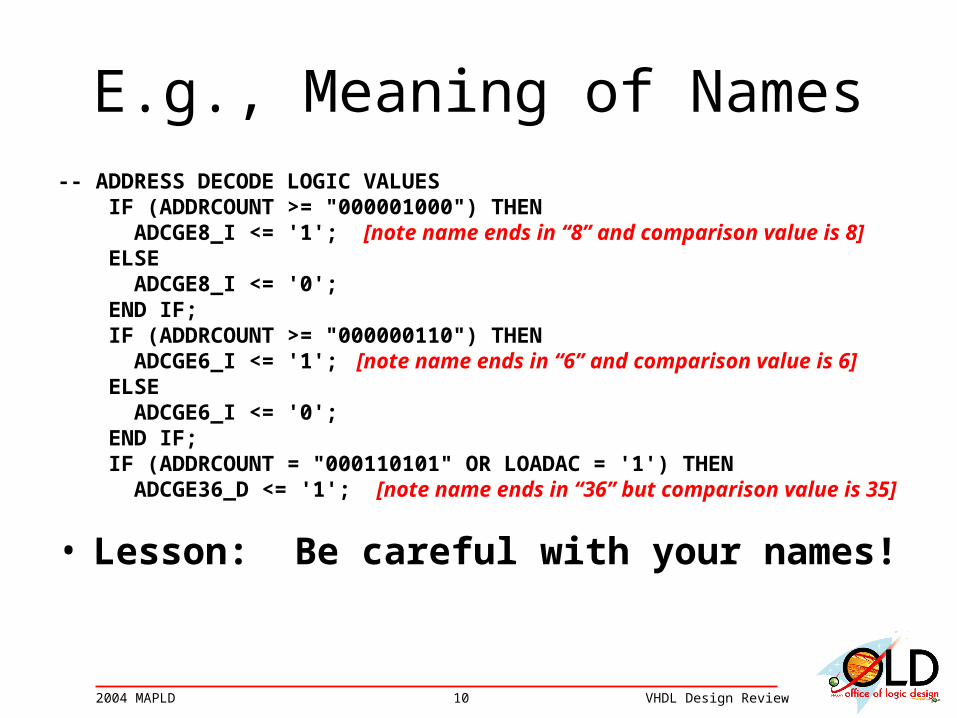
E.g., part of a 16 page process -- V1.02 & V2.2 -- DATA WILL STOP TANSFERING IFF BOTH HOLD AND OUTPUT ENABEL
ARE -- ACTIVE FOR THE SAME PORT
-- HOLD2 <= ((((HLD2TX_N_Q AND O_EN_Q(2)) OR -- (HLDTX_N_Q AND O_EN_Q(1)) OR -- (ROFRDY_N_Q AND O_EN_Q(0))) AND-- NOT(BYPASS_EN_Q AND (HLDTX_N_Q AND O_EN_Q(1)))));
HOLD1_I <= ((HLDTX_N_Q AND O_EN_Q(1)) OR (ROFRDY_N_Q AND O_EN_Q(0)));-- V2.2
HOLD2 <= (((((HLD2TX_N_Q AND O_EN_Q(2)) OR (HLDTX_N_Q AND O_EN_Q(1)) OR (ROFRDY_N_Q AND O_EN_Q(0))) AND NOT(BYPASS_EN_Q AND (HLDTX_N_Q AND O_EN_Q(1))))) OR (((HLD2TX_N_Q AND O_EN_Q(2)) OR (HLDTX_N_Q AND
O_EN_Q(1))) AND (BYPASS_EN_Q AND HLDTX_N_Q AND O_EN_Q(1))));
142004 MAPLD VHDL Design Review
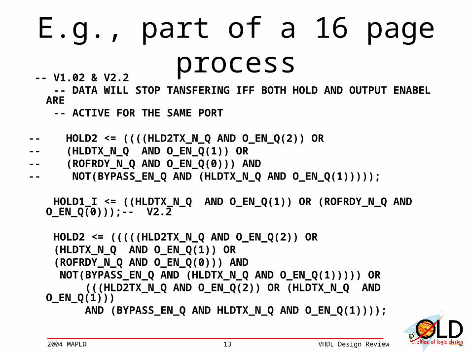
Simplifying
Let:a=HDL2TX_N_Q and O_EN_Q(2)b=HLDTX_N_Q and O_EN_Q(1)c=ROFRDY_N_Q and O_EN_Q(0)d=BYPASS_EN_Q
ThenHOLD2=(a+b+c)·(d·b)’ + (a+b)·(d·b) = a+b+c.
What happened to d=BYPASS_EN_Q??
152004 MAPLD VHDL Design Review
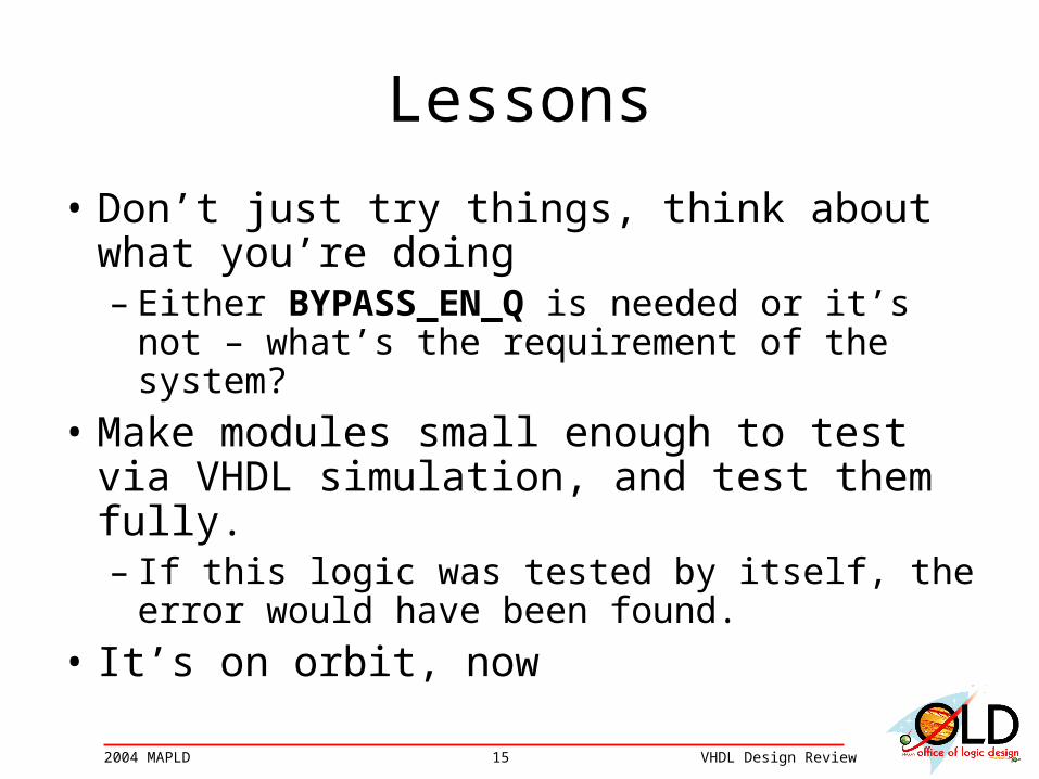
Lessons
• Don’t just try things, think about what you’re doing– Either BYPASS_EN_Q is needed or it’s not –
what’s the requirement of the system?
• Make modules small enough to test via VHDL simulation, and test them fully.– If this logic was tested by itself, the error
would have been found.
• It’s on orbit, now

162004 MAPLD VHDL Design Review
Combined Effects of VHDL
Hidden design details
+ Non-WYSIWYG nature
+ Bad design practicesDesigner can lose control of design
i.e., the designer loses understanding of what is in the design, then adds erroneous circuitry until simulation looks right
172004 MAPLD VHDL Design Review
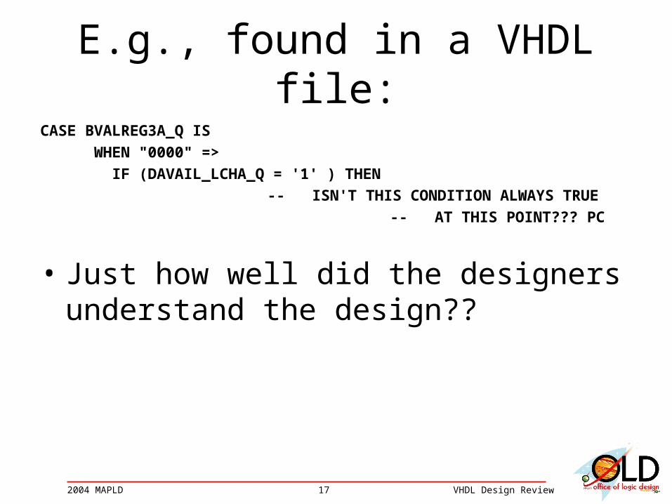
E.g., found in a VHDL file:
CASE BVALREG3A_Q IS
WHEN "0000" =>
IF (DAVAIL_LCHA_Q = '1' ) THEN
-- ISN'T THIS CONDITION ALWAYS TRUE
-- AT THIS POINT??? PC
• Just how well did the designers understand the design??
182004 MAPLD VHDL Design Review
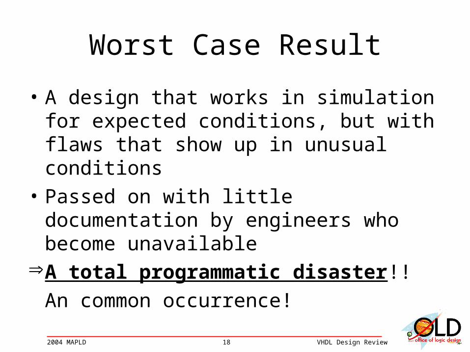
Worst Case Result
• A design that works in simulation for expected conditions, but with flaws that show up in unusual conditions
• Passed on with little documentation by engineers who become unavailable
A total programmatic disaster!!
An common occurrence!
192004 MAPLD VHDL Design Review
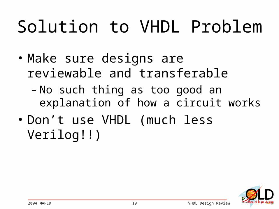
Solution to VHDL Problem
• Make sure designs are reviewable and transferable– No such thing as too good an explanation of
how a circuit works
• Don’t use VHDL (much less Verilog!!)

202004 MAPLD VHDL Design Review
VHDL Review
Tools and Techniques
212004 MAPLD VHDL Design Review
Netlist Viewer
• Crucial because– Synthesizer output, not VHDL, is the final
design– Easy to see asynchronous design items– Connectivity often more apparent in viewer
than in VHDL
• Helps solve the non-WYSIWYG nature of VHDL

222004 MAPLD VHDL Design Review
.srr files
• Flip-flop replication– See examples in “Synthesis Issues” module.
• State machine encoding and illegal state protection
• Inferred clocks => possible asynchronous design techniques
• Resource usage
232004 MAPLD VHDL Design Review
.adb files
• Needed for netlist viewer
• Check internal timing
• Get timing parameters to perform board level timing analysis
• Check I/O pin options

242004 MAPLD VHDL Design Review
VHDL Simulator
• Simulate modules or extract parts of modules
• Try to break them:– Most simulations are success oriented, in that
they try to show the module works when it gets the expected inputs
– Try to simulate with the unexpected inputs– Easier to do with smaller modules
252004 MAPLD VHDL Design Review
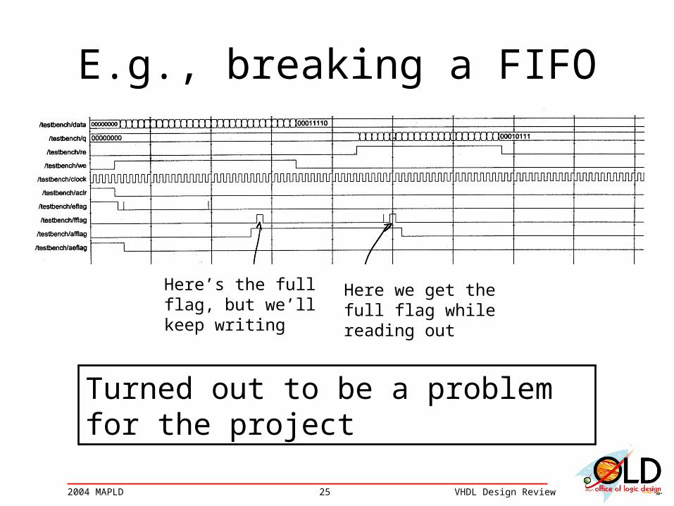
E.g., breaking a FIFO
Here’s the full flag, but we’ll keep writing
Here we get the full flag while reading out
Turned out to be a problem for the project

262004 MAPLD VHDL Design Review
Suggestions for FPGA Design Presentation

272004 MAPLD VHDL Design Review
Goals
• Detailed design review and worst-case analysis are the best tools for ensuring mission success.
• The goal here is not to make more work for the designer, but to:– Enhance efficiency of reviews– Make proof of design more clear– Make design more transferable– Improve design quality

282004 MAPLD VHDL Design Review
Steps to Preparing for Design Review
1. Modularize your design2. Make a datasheet for each module3. Show FPGA design in terms of modules4. Describe internal circuitry5. Describe state machines6. Describe FPGA connections7. Describe synthesis results8. Provide timing spec for external timing analysis9. Show requirements of external circuitry
292004 MAPLD VHDL Design Review
1. Modularize your design
• Easier to do during design phase• Goal is to describe design in terms of
components that can be individually verified• Each component, or module, is a separate
VHDL entity• Modules should be of moderate, e.g., MSI, size
– E.g., FIFO, ALU– Counter, decoder probably too small– VME interface too big

302004 MAPLD VHDL Design Review
2. Make a Datasheet for Each Module
• Describe the module’s behavior
• Show truth table
• Show timing diagrams of operation
• Provide test bench used to verify module– Try to break it
• Model: MSI part data sheet
312004 MAPLD VHDL Design Review
3. Show FPGA Design in Terms of Modules
• Provide requirements spec for FPGA• Draw block diagram• Top-level VHDL entity shows FPGA inputs and
outputs and ties component modules together• Show necessary timing diagrams
– Interaction between modules– Interaction with external circuitry
• Text for theory of operation• Provide test bench for top level simulation
322004 MAPLD VHDL Design Review
4. Describe internal circuitry
• Use of clock resources• Discuss skew issues• Describe deviations from fully synchronous
design– Be prepared to show necessary analysis
• Show how asynchronism is handled– External signals– Between clock domains
• Glitch analysis of output signals used as clocks by other parts

332004 MAPLD VHDL Design Review
5. Describe state machines
• Encoding chosen
• Protection against lock-up states
• Homing sequences
• Reset conditions

342004 MAPLD VHDL Design Review
6. Describe FPGA Connections• Use of special pins: TRST*, MODE, etc.• Power supply requirements
– Levels, sequencing, etc.
• Termination of unused clock pins• Input and output options chosen for pins• Discuss transition times of inputs• POR operation and circuitry• Critical signals and power-up conditions
– Remember WIRE! (being presented next door in a parallel seminar).
352004 MAPLD VHDL Design Review
7. Describe synthesis results
• Percentage of utilization
• Flip-flop replication and its effects on reliable operation
• Margin results from Timer
• Timing of circuits using both clock edges
362004 MAPLD VHDL Design Review
8. Provide Timing Specification for External Timing Analysis
• tSU, tH with respect to clock
• Clock to output tPD
• tPW for signals connected to flip-flop clocks
• Clock symmetry requirements if both edges of clock used

372004 MAPLD VHDL Design Review
9. Show Requirements of External Circuitry
• Provide data sheets for parts interfacing to FPGA
• Show timing diagrams of interactions of FPGA to other parts
• Show timing analysis of external circuitry

382004 MAPLD VHDL Design Review
References
• Design guidelines:http://klabs.org/DEI/References/design_guidelines/nasa_guidelines/
• Design tutorialshttp://klabs.org/richcontent/Tutorial/tutorial.htm
• Design, analysis, and test guidelines:http://klabs.org/DEI/References/design_guidelines/design_analysis_test_guides.htm
Related Documents